bq25895 I2C Controlled Single Cell 5-A Fast Charger …€¢ Power Bank, Mobile Wi-Fi Hotspot •...
64
SYS BAT bq25895 Host Input 3.9V–14V at 3A USB OTG 5V at 3.1A Ichg = 5A SYS 3.5V–4.5V I2C Bus Host Control VBUS SW TS QON Optional REGN Phone PMID Product Folder Order Now Technical Documents Tools & Software Support & Community An IMPORTANT NOTICE at the end of this data sheet addresses availability, warranty, changes, use in safety-critical applications, intellectual property matters and other important disclaimers. PRODUCTION DATA. bq25895 SLUSC88B – MARCH 2015 – REVISED MAY 2018 bq25895 I 2 C Controlled Single Cell 5-A Fast Charger with MaxCharge TM for High Input Voltage and Adjustable Voltage 3.1-A Boost Operation 1 1 Features 1• High Efficiency 5-A, 1.5-MHz Switch Mode Buck Charge – 93% Charge Efficiency at 2 A and 91% Charge Efficiency at 3 A Charge Current – Optimize for High Voltage Input (9 V to 12 V) – Low Power PFM mode for Light Load Operations • Boost Mode Operation with Adjustable Output from 4.5 V to 5.5 V – Selectable 500-KHz to 1.5-MHz Boost Converter with up to 3.1-A Output – 93% Boost Efficiency at 5 V at 1 A Output • Integrated Control to Switch Between Charge and Boost Mode • Single Input to Support USB Input and Adjustable High Voltage Adapters – Support 3.9-V to 14-V Input Voltage Range – Input Current Limit (100 mA to 3.25 A with 50- mA resolution) to Support USB2.0, USB3.0 standard and High Voltage Adapters – Maximum Power Tracking by Input Voltage Limit up-to 14V for Wide Range of Adapters – Auto Detect USB SDP, CDP, DCP, and Non- standard Adapters • Input Current Optimizer (ICO) to Maximize Input Power without Overloading Adapters • Resistance Compensation (IRCOMP) from Charger Output to Cell Terminal • Highest Battery Discharge Efficiency with 11-mΩ Battery Discharge MOSFET up to 9 A • Integrated ADC for System Monitor (Voltage, Temperature, Charge Current) • Narrow VDC (NVDC) Power Path Management – Instant-on Works with No Battery or Deeply Discharged Battery – Ideal Diode Operation in Battery Supplement Mode • BATFET Control to Support Ship Mode, Wake Up, and Full System Reset • Flexible Autonomous and I 2 C Mode for Optimal System Performance • High Integration includes all MOSFETs, Current Sensing and Loop Compensation • 12-μA Low Battery Leakage Current to Support Ship Mode • High Accuracy – ±0.5% Charge Voltage Regulation – ±5% Charge Current Regulation – ±7.5% Input Current Regulation • Safety – Battery Temperature Sensing for Charge and Boost Mode – Thermal Regulation and Thermal Shutdown – Create a Custom Design Using the bq25895 With the WEBENCH ® Power Designer 2 Applications • Power Bank, Mobile Wi-Fi Hotspot • Wireless Bluetooth Speaker • Portable Internet Devices 3 Description The bq25895 is a highly-integrated 5-A switch-mode battery charge management and system power path management device for single cell Li-Ion and Li- polymer battery. The devices support high input voltage fast charging. The low impedance power path optimizes switch-mode operation efficiency, reduces battery charging time and extends battery life during discharging phase. Device Information (1) PART NUMBER PACKAGE BODY SIZE (NOM) bq25895 WQFN (24) 4.00mm x 4.00mm (1) For all available packages, see the orderable addendum at the end of the datasheet. Simplified Schematic
-
Upload
duongthien -
Category
Documents
-
view
220 -
download
0
Transcript of bq25895 I2C Controlled Single Cell 5-A Fast Charger …€¢ Power Bank, Mobile Wi-Fi Hotspot •...

SYS
BAT
bq25895Host
Input3.9V±14V at 3A
USB
OTG5V at 3.1A
Ichg = 5A
SYS 3.5V±4.5V
I2C Bus
Host Control
VBUS SW
TS
QON
OptionalREGN
PhonePMID
Product
Folder
Order
Now
Technical
Documents
Tools &
Software
Support &Community
An IMPORTANT NOTICE at the end of this data sheet addresses availability, warranty, changes, use in safety-critical applications,intellectual property matters and other important disclaimers. PRODUCTION DATA.
bq25895SLUSC88B –MARCH 2015–REVISED MAY 2018
bq25895 I2C Controlled Single Cell 5-A Fast Charger with MaxChargeTM for High InputVoltage and Adjustable Voltage 3.1-A Boost Operation
1
1 Features1• High Efficiency 5-A, 1.5-MHz Switch Mode Buck
Charge– 93% Charge Efficiency at 2 A and 91% Charge
Efficiency at 3 A Charge Current– Optimize for High Voltage Input (9 V to 12 V)– Low Power PFM mode for Light Load
Operations• Boost Mode Operation with Adjustable Output
from 4.5 V to 5.5 V– Selectable 500-KHz to 1.5-MHz Boost
Converter with up to 3.1-A Output– 93% Boost Efficiency at 5 V at 1 A Output
• Integrated Control to Switch Between Charge andBoost Mode
• Single Input to Support USB Input and AdjustableHigh Voltage Adapters– Support 3.9-V to 14-V Input Voltage Range– Input Current Limit (100 mA to 3.25 A with 50-
mA resolution) to Support USB2.0, USB3.0standard and High Voltage Adapters
– Maximum Power Tracking by Input VoltageLimit up-to 14V for Wide Range of Adapters
– Auto Detect USB SDP, CDP, DCP, and Non-standard Adapters
• Input Current Optimizer (ICO) to Maximize InputPower without Overloading Adapters
• Resistance Compensation (IRCOMP) fromCharger Output to Cell Terminal
• Highest Battery Discharge Efficiency with 11-mΩBattery Discharge MOSFET up to 9 A
• Integrated ADC for System Monitor(Voltage, Temperature, Charge Current)
• Narrow VDC (NVDC) Power Path Management– Instant-on Works with No Battery or Deeply
Discharged Battery– Ideal Diode Operation in Battery Supplement
Mode• BATFET Control to Support Ship Mode, Wake Up,
and Full System Reset• Flexible Autonomous and I2C Mode for Optimal
System Performance• High Integration includes all MOSFETs, Current
Sensing and Loop Compensation• 12-µA Low Battery Leakage Current to Support
Ship Mode• High Accuracy
– ±0.5% Charge Voltage Regulation– ±5% Charge Current Regulation– ±7.5% Input Current Regulation
• Safety– Battery Temperature Sensing for Charge and
Boost Mode– Thermal Regulation and Thermal Shutdown– Create a Custom Design Using the bq25895
With the WEBENCH® Power Designer
2 Applications• Power Bank, Mobile Wi-Fi Hotspot• Wireless Bluetooth Speaker• Portable Internet Devices
3 DescriptionThe bq25895 is a highly-integrated 5-A switch-modebattery charge management and system power pathmanagement device for single cell Li-Ion and Li-polymer battery. The devices support high inputvoltage fast charging. The low impedance power pathoptimizes switch-mode operation efficiency, reducesbattery charging time and extends battery life duringdischarging phase.
Device Information(1)
PART NUMBER PACKAGE BODY SIZE (NOM)bq25895 WQFN (24) 4.00mm x 4.00mm
(1) For all available packages, see the orderable addendum atthe end of the datasheet.
Simplified Schematic

2
bq25895SLUSC88B –MARCH 2015–REVISED MAY 2018 www.ti.com
Product Folder Links: bq25895
Submit Documentation Feedback Copyright © 2015–2018, Texas Instruments Incorporated
Table of Contents1 Features .................................................................. 12 Applications ........................................................... 13 Description ............................................................. 14 Revision History..................................................... 35 Description (continued)......................................... 36 Pin Configuration and Functions ......................... 47 Specifications......................................................... 6
7.1 Absolute Maximum Ratings ...................................... 67.2 ESD Ratings.............................................................. 67.3 Recommended Operating Conditions....................... 67.4 Thermal Information .................................................. 77.5 Electrical Characteristics........................................... 77.6 Timing Requirements .............................................. 117.7 Typical Characteristics ............................................ 12
8 Detailed Description ............................................ 148.1 Functional Block Diagram ....................................... 148.2 Feature Description................................................. 158.3 Device Functional Modes........................................ 30
8.4 Register Maps ......................................................... 329 Application and Implementation ........................ 49
9.1 Application Information............................................ 499.2 Typical Application .................................................. 499.3 System Examples ................................................... 54
10 Power Supply Recommendations ..................... 5511 Layout................................................................... 55
11.1 Layout Guidelines ................................................. 5511.2 Layout Example .................................................... 55
12 Device and Documentation Support ................. 5612.1 Development Support ........................................... 5612.2 Receiving Notification of Documentation Updates 5612.3 Community Resources.......................................... 5612.4 Trademarks ........................................................... 5612.5 Electrostatic Discharge Caution............................ 5612.6 Glossary ................................................................ 56
13 Mechanical, Packaging, and OrderableInformation ........................................................... 56

3
bq25895www.ti.com SLUSC88B –MARCH 2015–REVISED MAY 2018
Product Folder Links: bq25895
Submit Documentation FeedbackCopyright © 2015–2018, Texas Instruments Incorporated
4 Revision History
Changes from Revision A (May 216) to Revision B Page
• Added "SW (peak for 10 ns duration)" To the Absolute Maximum Rating ............................................................................ 6• Updated the Thermal Information values ............................................................................................................................... 7• Changed VSYS TYP value From: VBAT + 50 mV To: I(SYS) + 150 mV ...................................................................................... 7• Changed the title of Figure 4 From: Charge Current Accuracy To: I2C Setting .................................................................. 12• Changed axis title of Figure 8 From: BAT Voltage (V) To: Input Current Limit (mA) ........................................................... 12• Changed VVREF to VREGN in Figure 15................................................................................................................................... 23• Changed VVREF to VREGN in Equation 2................................................................................................................................. 23• Changed VREF to VREGN in Figure 16 .................................................................................................................................... 24• Added sentence to the Battery Monitor secton "In battery only mode, .."............................................................................ 24• Changed bit 5 From: 0 To: 1 in Figure 29 ............................................................................................................................ 35• Changed the Description values of Table 26 From: mV To: mA.......................................................................................... 47• Changed the Type values of Bits 6 to Bit 0 in Table 28 From: R/W To: R .......................................................................... 48• Added VREF system pullup voltage to Table 29 .................................................................................................................... 49• Changed Figure 49............................................................................................................................................................... 52
Changes from Original (March 2015) to Revision A Page
• Added Pin Configuration and Functions section, ESD Rating table, Feature Description section, Device FunctionalModes, Application and Implementation section, Power Supply Recommendations section, Layout section, Deviceand Documentation Support section, and Mechanical, Packaging, and Orderable Information section. .............................. 1
5 Description (continued)The I2C Serial interface with charging and system settings makes the device a truly flexible solution.
The device supports a wide range of input sources, including standard USB host port, USB charging port, andUSB compliant adjustable high voltage adapter. To support fast charging using adjustable high voltage adapter,the bq25895 provides support MaxChargeTM using D+/D– pins and DSEL pin for USB switch control. In addition,the device includes interface to support adjustable high voltage adapter using input current pulse protocol. To setthe default input current limit, device uses the built-in USB interface. The device is compliant with USB 2.0 andUSB 3.0 power spec with input current and voltage regulation. In addition, the Input Current Optimizer (ICO)supports the detection of maximum power point detection of the input source without overload. The devicesupports battery boost operation by supplying adjustable 4.5 V to 5.5 V on PMID pin with up to 3.1 A withintegrated charge and boost mode detection

STAT
SCL
SDA
PM
ID
RE
GN
PGND
PGND
SYS
SYSO
TG
INT
4
5
6
7 8 9
15
16
17
18
222324
1
2
3
BAT
BAT13
14
BT
ST
SW
SW
192021
10 11 12
VBUS
D+
D–
ILIM TS
CE
DS
EL
QO
N
4
bq25895SLUSC88B –MARCH 2015–REVISED MAY 2018 www.ti.com
Product Folder Links: bq25895
Submit Documentation Feedback Copyright © 2015–2018, Texas Instruments Incorporated
6 Pin Configuration and Functions
bq25895RTW (WQFN)
Top View
(1) DI (Digital Input), DO (Digital Output), DIO (Digital Input/Output), AI (Analog Input), AO (Analog Output), AIO (Analog Input/Output)
Pin FunctionsPIN
TYPE (1) DESCRIPTIONNAME NO.
VBUS 1 PCharger Input Voltage.The internal n-channel reverse block MOSFET (RBFET) is connected between VBUS and PMID with VBUS onsource. Place a 1-µF ceramic capacitor from VBUS to PGND and place it as close as possible to IC.
D+ 2 AIOPositive line of the USB data line pair.D+/D- based USB host/charging port detection. The detection includes data contact detection (DCD), primaryand secondary detection in BC1.2, and Adjustable high voltage adapter (MaxCharge).
D– 3 AIONegative line of the USB data line pair.D+/D- based USB host/charging port detection. The detection includes data contact detection (DCD), primaryand secondary detection in BC1.2, and Adjustable high voltage adapter (MaxCharge).
STAT 4 DO
Open drain charge status output to indicate various charger operation.Connect to the pull up rail via 10-kΩ resistor. LOW indicates charge in progress. HIGH indicates chargecomplete or charge disabled. When any fault condition occurs, STAT pin blinks in 1 Hz.The STAT pin function can be disabled when STAT_DIS bit is set.
SCL 5 DI I2C Interface clock.Connect SCL to the logic rail through a 10-kΩ resistor.
SDA DIO I2C Interface data.Connect SDA to the logic rail through a 10-kΩ resistor.
INT 7 DOOpen-drain Interrupt Output.Connect the INT to a logic rail via 10-kΩ resistor. The INT pin sends active low, 256-µs pulse to host to reportcharger device status and fault.
OTG 8 DIBoost mode enable pin.The boost mode is activated when OTG_CONFIG =1, OTG pin is high, and no input source is detected atVBUS
CE 9 DI Active low Charge Enable pin.Battery charging is enabled when CHG_CONFIG = 1 and CE pin = Low. CE pin must be pulled High or Low.

5
bq25895www.ti.com SLUSC88B –MARCH 2015–REVISED MAY 2018
Product Folder Links: bq25895
Submit Documentation FeedbackCopyright © 2015–2018, Texas Instruments Incorporated
Pin Functions (continued)PIN
TYPE (1) DESCRIPTIONNAME NO.
ILIM 10 AI
Input current limit Input. ILIM pin sets the maximum input current and can be used to monitor input currentILIM pin sets the maximum input current limit by regulating the ILIM voltage at 0.8 V. A resistor is connectedfrom ILIM pin to ground to set the maximum limit as IINMAX = KILIM/RILIM . The actual input current limit is thelower limit set by ILIM pin (when EN_ILIM bit is high) or IIINLIM register bits. Input current limit of less than 500mA is not support on ILIM pin.ILIM pin can also be used to monitor input current when the voltage is below 0.8V. The input current isproportional to the voltage on ILIM pin and can be calculated by IIN = (KILIM x VILIM) / (RILIM x 0.8)The ILIM pin function can be disabled when EN_ILIM bit is 0.
TS 11 AI
Temperature qualification voltage input.Connect a negative temperature coefficient thermistor. Program temperature window with a resistor dividerfrom REGN to TS to GND. Charge suspends when either TS pin is out of range. Recommend 103AT-2thermistor.
QON 12 DI
BATFET enable/reset control input.When BATFET is in ship mode, a logic low of tSHIPMODE (typical 1sec) duration turns on BATFET to exitshipping mode. .When VBUS is not plugged-in, a logic low of tQON_RST (typical 10sec) duration resets SYS (system power) byturning BATFET off for tBATFET_RST (typical 0.3sec) and then re-enable BATFET to provide full system powerreset.The pin contains an internal pull-up to maintain default high logic
BAT 13,14 P Battery connection point to the positive terminal of the battery pack.The internal BATFET is connected between BAT and SYS. Connect a 10uF closely to the BAT pin.
SYS 15,16 P
System connection point.The internal BATFET is connected between BAT and SYS. When the battery falls below the minimum systemvoltage, switch-mode converter keeps SYS above the minimum system voltage. Connect a 20uF closely to theSYS pin.
PGND 17,18 P
Power ground connection for high-current power converter node.Internally, PGND is connected to the source of the n-channel LSFET. On PCB layout, connect directly toground connection of input and output capacitors of the charger. A single point connection is recommendedbetween power PGND and the analog GND near the IC PGND pin.
SW 19,20 PSwitching node connecting to output inductor.Internally SW is connected to the source of the n-channel HSFET and the drain of the n-channel LSFET.Connect the 0.047µF bootstrap capacitor from SW to BTST.
BTST 21 PPWM high side driver positive supply.Internally, the BTST is connected to the anode of the boost-strap diode. Connect the 0.047µF bootstrapcapacitor from SW to BTST.
REGN 22 P
PWM low side driver positive supply output.Internally, REGN is connected to the cathode of the boost-strap diode. Connect a 4.7µF (10 V rating) ceramiccapacitor from REGN to analog GND. The capacitor should be placed close to the IC. REGN also serves asbias rail of TS pin.
PMID 23 DOBattery boost mode output.Connected to the drain of the reverse blocking MOSFET (RBFET) and the drain of HSFET. The minimumcapacitance required on PMID to PGND is 40µF for up-to 2.4A output and 60µF for up-to 3.1A output
DSEL 24 DO
Open-drain D+/D- multiplexer selection control.Connect the DSEL to a logic rail via 10-KΩ resistor. The pin is normally float and pull-up by external resistor.During Input Source Type Detection , the pin drives low to indicate the device D+/D- detection is in progressand needs to take control of D+, D- signals. When detection is completed, the pin keeps low when MaxChargeis detected. The pin returns to float and pulls high by external resistor when other input source type is detected.
PowerPAD™ P Exposed pad beneath the IC for heat dissipation. Always solder PowerPAD Pad to the board, and have vias onthe PowerPAD plane star-connecting to PGND and ground plane for high-current power converter.

6
bq25895SLUSC88B –MARCH 2015–REVISED MAY 2018 www.ti.com
Product Folder Links: bq25895
Submit Documentation Feedback Copyright © 2015–2018, Texas Instruments Incorporated
(1) Stresses beyond those listed under absolute maximum ratings may cause permanent damage to the device. These are stress ratingsonly, and functional operation of the device at these or any other conditions beyond those indicated under recommended operatingconditions is not implied. Exposure to absolute-maximum-rated conditions for extended periods may affect device reliability. All voltagevalues are with respect to the network ground terminal unless otherwise noted.
7 Specifications
7.1 Absolute Maximum Ratings (1)
over operating free-air temperature range (unless otherwise noted)MIN MAX VALUE
Voltage range (with respect to GND)
VBUS (converter not switching) –2 22 VPMID (converter not switching) –0.3 22 VSTAT –0.3 20 VDSEL –0.3 20 VBTST –0.3 20 VSW –2 16 VSW (peak for 10 ns duration) –3 16 VBAT, SYS (converter not switching) –0.3 6 VSDA, SCL, INT, OTG, REGN, TS, CE, QON –0.3 7 VD+, D– –0.3 7 VBTST TO SW –0.3 7 VPGND to GND –0.3 0.3 VILIM –0.3 5 V
Output sink currentINT, STAT 6 mADSEL 6 mA
Junction temperature –40 150 °CStorage temperature range, Tstg –65 150 °C
(1) JEDEC document JEP155 states that 500-V HBM allows safe manufacturing with a standard ESD control process.(2) JEDEC document JEP157 states that 250-V CDM allows safe manufacturing with a standard ESD control process.
7.2 ESD RatingsVALUE UNIT
VESD Electrostatic dischargeHuman body model (HBM), per ANSI/ESDA/JEDEC JS-001 (1) ±2000 VCharged device model (CDM), per JEDEC specificationJESD22-C101 (2) ±250 V
(1) The inherent switching noise voltage spikes should not exceed the absolute maximum rating on either the BTST or SW pins. A tightlayout minimizes switching noise.
7.3 Recommended Operating Conditionsover operating free-air temperature range (unless otherwise noted)
MIN NOM MAX UNITVIN Input voltage 3.9 14 (1) VIIN Input current (VBUS) 3.25 AISYS Output current (SW) 5 AVBAT Battery voltage 4.608 V
IBAT
Fast charging current 5 A
Discharging current with internal MOSFETUp to 6 (continuos) A
9 (peak)(Up to 1 sec duration) A
TA Operating free-air temperature range –40 85 °C

7
bq25895www.ti.com SLUSC88B –MARCH 2015–REVISED MAY 2018
Product Folder Links: bq25895
Submit Documentation FeedbackCopyright © 2015–2018, Texas Instruments Incorporated
(1) For more information about traditional and new thermal metrics, see the Semiconductor and IC Package Thermal Metrics applicationreport.
7.4 Thermal Information
THERMAL METRIC (1)bq25895
UNITRTW (WQFN)24-PINS
RθJA Junction-to-ambient thermal resistance 31.8 °C/WRθJC((op) Junction-to-case (top) thermal resistance 27.9 °C/WRθJB Junction-to-board thermal resistance 8.7 °C/WψJT Junction-to-top characterization parameter 0.3 °C/WψJB Junction-to-board characterization parameter 8.7 °C/WRθJC(bot) Junction-to-case (bottom) thermal resistance 2.0 °C/W
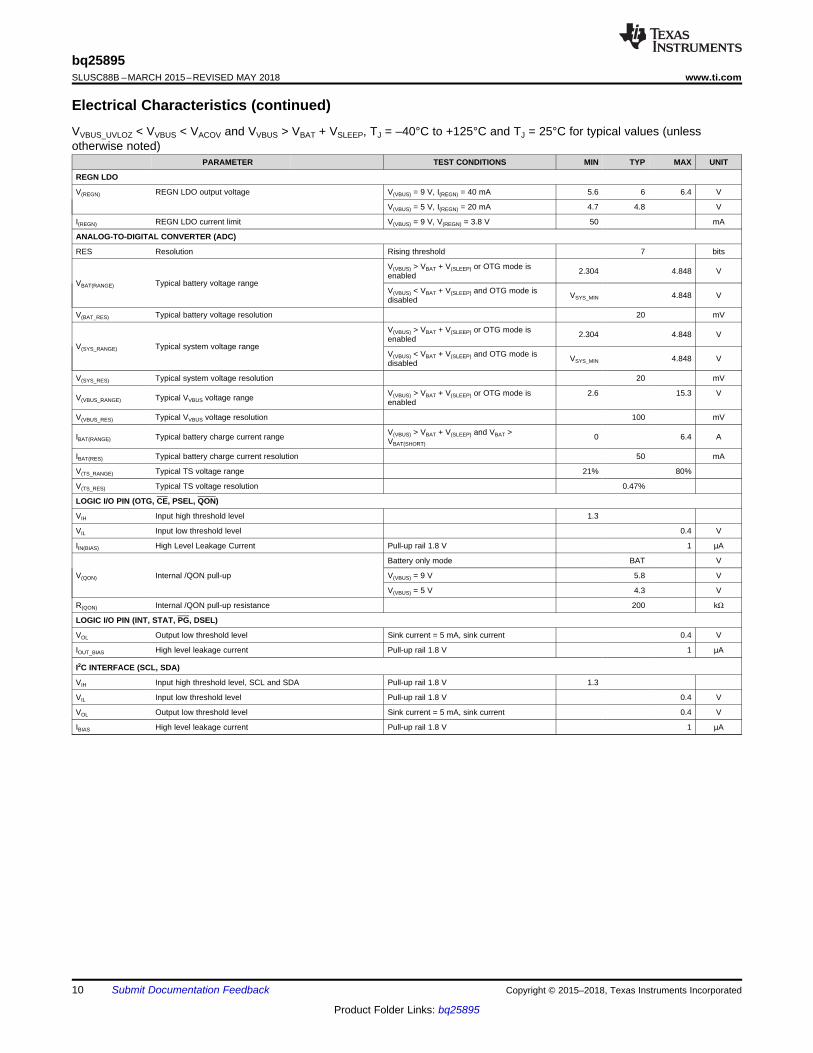
7.5 Electrical CharacteristicsVVBUS_UVLOZ < VVBUS < VACOV and VVBUS > VBAT + VSLEEP, TJ = –40°C to +125°C and TJ = 25°C for typical values (unlessotherwise noted)
PARAMETER TEST CONDITIONS MIN TYP MAX UNIT
QUIESCENT CURRENTS
IBAT Battery discharge current (BAT, SW, SYS) in buck mode
VBAT = 4.2 V, V(VBUS) < V(UVLO), leakagebetween BAT and VBUS 5 µA
High-Z mode, no VBUS, BATFET disabled(REG09[5]=1), battery monitor disabled, TJ <85°C
12 23 µA
High-Z mode, no VBUS, BATFET enabled(REG09[5]=0), battery monitor disabled, TJ <85°C
32 60 µA
I(VBUS_HIZ)Input supply current (VBUS) in buck mode when High-Z modeis enabled
V(VBUS)= 5 V, High-Z mode, no battery, batterymonitor disabled 15 35 µA
V(VBUS)= 12 V, High-Z mode, no battery,battery monitor disabled 25 50 µA
I(VBUS) Input supply current (VBUS) in buck mode
VBUS > V(UVLO), VBUS > VBAT, converter notswitching 1.5 3 mA
VBUS > V(UVLO), VBUS > VBAT, converterswitching, VBAT = 3.2 V, ISYS = 0A 3 mA
VBUS > V(UVLO), VBUS > VBAT, converterswitching, VBAT = 3.8 V, ISYS = 0 A 3 mA
I(BOOST) Battery discharge current in boost mode VBAT = 4.2 V, boost mode, I(VBUS)= 0 A,converter switching 5 mA
VBUS/BAT POWER UP
V(VBUS_OP) VBUS operating range 3.9 14 V
V(VBUS_UVLOZ) VBUS for active I2C, no battery 3.6 V
V(SLEEP) Sleep mode falling threshold 25 65 120 mV
V(SLEEPZ) Sleep mode rising threshold 130 250 370 mV
V(ACOV)
VBUS over-voltage rising threshold 14 14.6 V
VBUS over-voltage falling threshold 13.5 14 V
VBAT(UVLOZ) Battery for active I2C, no VBUS 2.3 V
VBAT(DPL) Battery depletion falling threshold 2.15 2.5 V
VBAT(DPLZ) Battery depletion rising threshold 2.35 2.7 V
V(VBUSMIN) Bad adapter detection threshold 3.8 V
I(BADSRC) Bad adapter detection current source 30 mA
POWER-PATH MANAGEMENT
VSYS Typical system regulation voltage
I(SYS) = 0 A, VBAT> VSYS(MIN), BATFET Disabled(REG09[5]=1)
VBAT+50 mV V
I(SYS) = 0 A, VBAT< VSYS(MIN), BATFET Disabled(REG09[5]=1)
VSYS(MIN) +150 mV V
VSYS(MIN) Minimum DC system voltage output VBAT< VSYS(MIN), SYS_MIN = 3.5 V(REG03[3:1]=101), ISYS= 0 A 3.50 3.65 V
VSYS(MAX) Maximum DC system voltage output VBAT = 4.35 V, SYS_MIN = 3.5V(REG03[3:1]=101), ISYS= 0 A 4.40 4.42 V
RON(RBFET)Top reverse blocking MOSFET(RBFET) on-resistancebetween VBUS and PMID
TJ = –40°C to +85°C 27 38 mΩ
TJ = –40°C to +125°C 27 44 mΩ

8
bq25895SLUSC88B –MARCH 2015–REVISED MAY 2018 www.ti.com
Product Folder Links: bq25895
Submit Documentation Feedback Copyright © 2015–2018, Texas Instruments Incorporated
Electrical Characteristics (continued)VVBUS_UVLOZ < VVBUS < VACOV and VVBUS > VBAT + VSLEEP, TJ = –40°C to +125°C and TJ = 25°C for typical values (unlessotherwise noted)
PARAMETER TEST CONDITIONS MIN TYP MAX UNIT
RON(HSFET)Top switching MOSFET (HSFET) on-resistance between PMIDand SW
TJ = –40°C to +85°C 27 39 mΩ
TJ = –40°C to +125°C 27 47 mΩ
RON(LSFET)Bottom switching MOSFET (LSFET) on-resistance betweenSW and GND
TJ = –40°C to +85°C 16 24 mΩ
TJ = –40°C to +125°C 16 28 mΩ
V(FWD) BATFET forward voltage in supplement mode BAT discharge current 10 mA 30 mV
VBAT(GD) Battery good comparator rising threshold VBAT rising 3.4 3.55 3.7 V
VBAT(GD_HYST) Battery good comparator falling threshold VBAT falling 100 mV
BATTERY CHARGER
VBAT(REG_RANGE) Typical charge voltage range 3.840 4.608 V
VBAT(REG_STEP) Typical charge voltage step 16 mV
VBAT(REG) Charge voltage resolution accuracyVBAT = 4.208 V (REG06[7:2]=010111) orVBAT = 4.352 V (REG06[7:2]=100000)TJ = –40°C to +85°C
-0.5% 0.5%
I(CHG_REG__RANGE) Typical fast charge current regulation range 0 5056 mA
I(CHG_REG_STEP) Typical fast charge current regulation step 64 mA
I(CHG_REG_ACC) Fast charge current regulation accuracy
VBAT = 3.1 V or 3.8 V, ICHG = 128 mATJ = –40°C to +85°C -20% 20%
VBAT= 3.1 V or 3.8 V, ICHG = 256 mATJ = –40°C to +85°C -10% 10%
VBAT= 3.1 V or 3.8 V, ICHG=1792 mATJ = –40°C to +85°C -5% 5%
VBAT(LOWV)
Battery LOWV falling threshold Fast charge to precharge, BATLOWV(REG06[1]) = 1 2.6 2.8 2.9 V
Battery LOWV rising threshold Precharge to fast charge, BATLOWV(REG06[1])=1(Typical 200-mV hysteresis)
2.8 3 3.1 V
I(PRECHG_RANGE) Precharge current range 64 1024 mA
I(PRECHG_STEP) Typical precharge current step 64 mA
I(PRECHG_ACC) Precharge current accuracy VBAT=2.6 V, IPRECHG = 256 mA –10% +10%
I(TERM_RANGE) Termination current range 64 1024 mA
I(TERM_STEP) Typical termination current step 64 mA
I(TERM_ACC) Termination current accuracy
ITERM = 256 mA, ICHG<= 1344 mATJ = –20°C to +85°C –12% 12%
ITERM = 256 mA, ICHG> 1344 mATJ = –20°C to +85°C –20% 20%
V(SHORT) Battery short voltage VBAT falling 2 V
V(SHORT_HYST) Battery short voltage hysteresis VBAT rising 200 mV
I(SHORT) Battery short current VBAT < 2.2 V 100 mA
V(RECHG) Recharge threshold below VBATREG
VBAT falling, VRECHG (REG06[0]=0) = 0 100 mV
VBAT falling, VRECHG (REG06[0]=0) = 1 200 mV
IBAT(LOAD) Battery discharge load current VBAT = 4.2 V 15 mA
ISYS(LOAD) System discharge load current VSYS = 4.2 V 30 mA
RON(BATFET) SYS-BAT MOSFET (BATFET) on-resistanceTJ = 25°C 11 13 mΩ
TJ = –40°C to +125°C 11 19 mΩ
INPUT VOLTAGE / CURRENT REGULATION
VIN(DPM_RANGE) Typical Input voltage regulation range 3.9 15.3 V
VIN(DPM_STEP) Typical Input voltage regulation step 100 mV
VIN(DPM_ACC) Input voltage regulation accuracy VINDPM = 4.4 V, 9 V 3% 3%
IIN(DPM_RANGE) Typical Input current regulation range 100 3250 mA
IIN(DPM_STEP) Typical Input current regulation step 50 mA
IIN(DPM100_ACC) Input current 100-mA regulation accuracyVBAT = 5 V, current pulled from SW
IINLIM (REG00[5:0]) =100 mA 85 90 100 mA
IIN(DPM_ACC)Input current regulation accuracyVBAT = 5 V, current pulled from SW
USB150, IINLIM (REG00[5:0]) = 150 mA 125 135 150 mA
USB500, IINLIM (REG00[5:0]) = 500 mA 440 470 500 mA
USB900, IINLIM (REG00[5:0]) = 900 mA 750 825 900 mA
Adapter 1.5 A, IINLIM (REG00[5:0]) = 1500mA 1300 1400 1500 mA
IIN(START) Input current regulation during system start up VSYS = 2.2 V, IINLIM (REG00[5:0])> = 200 mA 200 mA

9
bq25895www.ti.com SLUSC88B –MARCH 2015–REVISED MAY 2018
Product Folder Links: bq25895
Submit Documentation FeedbackCopyright © 2015–2018, Texas Instruments Incorporated
Electrical Characteristics (continued)VVBUS_UVLOZ < VVBUS < VACOV and VVBUS > VBAT + VSLEEP, TJ = –40°C to +125°C and TJ = 25°C for typical values (unlessotherwise noted)
PARAMETER TEST CONDITIONS MIN TYP MAX UNIT
KILIM IINMAX = KILIM/RILIM Input current regulation by ILIM pin = 1.5 A 320 355 390 A x Ω
D+/D- DETECTION
V(0P6_VSRC) D+/D– voltage source (0.6 V) 0.5 0.6 0.7 V
V(3p45_VSRC) D+/D– voltage source (3.45 V) 3.3 3.45 3.6 V
I(10UA_ISRC) D+ connection check current source 7 10 14 µA
I(100UA_ISINK) D+/D– current sink (100 µA) 50 100 150 µA
I(DPDM_LKG) D+/D– Leakage current D–, switch open –1 1 µA
D+, switch open –1 1 µA
I(1P6MA_ISINK) D+/D– current sink (1.6 mA) 1.45 1.60 1.75 µA
V(0P4_VTH) D+/D– low comparator threshold 250 400 mV
V(0P8_VTH) D+ low comparator threshold 0.8 V
V(2P7_VTH) D+/D– comparator threshold for non-standard adapterdetection (divider 1, 3, or 4)
2.55 2.85 V
V(2P0_VTH) D+/D– comparator threshold for non-standard adapterdetection (divider 1, 3)
1.85 2.15 V
V(1P2_VTH) D+/D– comparator threshold for non-standard adapterdetection (divider 2)
1.05 1.35 V
R(D–_DWN) D– pulldown for connection check 14.25 24.8 kΩ
BAT OVER-VOLTAGE/CURRENT PROTECTION
VBAT(OVP) Battery over-voltage threshold VBAT rising, as percentage of VBAT(REG) 104%
VBAT(OVP_HYST) Battery over-voltage hysteresis VBAT falling, as percentage of VBAT(REG) 2%
IBAT(FET_OCP) System over-current threshold 9 A
THERMAL REGULATION AND THERMAL SHUTDOWN
TREG Junction temperature regulation accuracy REG08[1:0] = 11 120 °C
TSHUT Thermal shutdown rising temperature Temperature rising 160 °C
TSHUT(HYS) Thermal shutdown hysteresis Temperature falling 30 °C
V(LTF) Cold temperature threshold, TS pin voltage rising threshold As percentage to V(REGN) 72.75% 73.25% 73.75%
V(LTF_HYS) Cold temperature hysteresis, TS pin voltage falling As percentage to V(REGN) 0.4%
V(HTF) Hot temperature TS pin voltage rising threshold As percentage to V(REGN) 47.75% 48.25% 48.75%
V(TCO) Cut-off temperature TS pin voltage falling threshold As percentage to V(REGN) 44.25% 44.75% 45.25%
COLD/HOT THERMISTOR COMPARATOR (BOOST MODE)
V(BCOLD1) Cold temperature threshold 1, TS pin voltage rising threshold As percentage to VREGN REG01[5] = 1(Approximately –20°C w/ 103AT) 79.5% 80% 80.5%
V(BCOLD1_HYS) Cold temperature threshold 1, TS pin voltage falling threshold As percentage to VREGN REG01[5] = 1 1%
V(BHOT2) Hot temperature threshold 2, TS pin voltage falling threshold As percentage to VREGN REG01[7:6] = 10(Approx. 65°C w/ 103AT) 30.75% 31.25% 31.75%
V(BHOT2_HYS) Hot temperature threshold 2, TS pin voltage rising threshold As percentage to VREGN REG01[7:6] =10 3%
PWM
FSW PWM switching frequency, and digital clock Oscillator frequency 1.32 1.68 MHz
DMAX Maximum PWM duty cycle 97%
BOOST MODE OPERATION
V(OTG_REG_RANGE) Typical boost mode regulation voltage range 4.55 5.55 V
V(OTG_REG_STEP) Typical boost mode regulation voltage step 64 mV
V(OTG_REG_ACC) Boost mode regulation voltage accuracy I(PMID) = 0 A, BOOSTV=5.126V (REG0A[7:4]= 1001) –3% 3%
V(OTG_BAT) Battery voltage exiting boost mode BAT falling 2.6 2.9 V
I(OTG) Boost mode output current range 3.1 A
V(OTG_OVP) Boost mode over-voltage threshold Rising threshold 5.8 6 V
10
bq25895SLUSC88B –MARCH 2015–REVISED MAY 2018 www.ti.com
Product Folder Links: bq25895
Submit Documentation Feedback Copyright © 2015–2018, Texas Instruments Incorporated
Electrical Characteristics (continued)VVBUS_UVLOZ < VVBUS < VACOV and VVBUS > VBAT + VSLEEP, TJ = –40°C to +125°C and TJ = 25°C for typical values (unlessotherwise noted)
PARAMETER TEST CONDITIONS MIN TYP MAX UNIT
REGN LDO
V(REGN) REGN LDO output voltage V(VBUS) = 9 V, I(REGN) = 40 mA 5.6 6 6.4 V
V(VBUS) = 5 V, I(REGN) = 20 mA 4.7 4.8 V
I(REGN) REGN LDO current limit V(VBUS) = 9 V, V(REGN) = 3.8 V 50 mA
ANALOG-TO-DIGITAL CONVERTER (ADC)
RES Resolution Rising threshold 7 bits
VBAT(RANGE) Typical battery voltage range
V(VBUS) > VBAT + V(SLEEP) or OTG mode isenabled 2.304 4.848 V
V(VBUS) < VBAT + V(SLEEP) and OTG mode isdisabled VSYS_MIN 4.848 V
V(BAT_RES) Typical battery voltage resolution 20 mV
V(SYS_RANGE) Typical system voltage range
V(VBUS) > VBAT + V(SLEEP) or OTG mode isenabled 2.304 4.848 V
V(VBUS) < VBAT + V(SLEEP) and OTG mode isdisabled VSYS_MIN 4.848 V
V(SYS_RES) Typical system voltage resolution 20 mV
V(VBUS_RANGE) Typical VVBUS voltage range V(VBUS) > VBAT + V(SLEEP) or OTG mode isenabled
2.6 15.3 V
V(VBUS_RES) Typical VVBUS voltage resolution 100 mV
IBAT(RANGE) Typical battery charge current range V(VBUS) > VBAT + V(SLEEP) and VBAT >VBAT(SHORT)
0 6.4 A
IBAT(RES) Typical battery charge current resolution 50 mA
V(TS_RANGE) Typical TS voltage range 21% 80%
V(TS_RES) Typical TS voltage resolution 0.47%
LOGIC I/O PIN (OTG, CE, PSEL, QON)
VIH Input high threshold level 1.3
VIL Input low threshold level 0.4 V
IIN(BIAS) High Level Leakage Current Pull-up rail 1.8 V 1 µA
V(QON) Internal /QON pull-up
Battery only mode BAT V
V(VBUS) = 9 V 5.8 V
V(VBUS) = 5 V 4.3 V
R(QON) Internal /QON pull-up resistance 200 kΩ
LOGIC I/O PIN (INT, STAT, PG, DSEL)
VOL Output low threshold level Sink current = 5 mA, sink current 0.4 V
IOUT_BIAS High level leakage current Pull-up rail 1.8 V 1 µA
I2C INTERFACE (SCL, SDA)
VIH Input high threshold level, SCL and SDA Pull-up rail 1.8 V 1.3
VIL Input low threshold level Pull-up rail 1.8 V 0.4 V
VOL Output low threshold level Sink current = 5 mA, sink current 0.4 V
IBIAS High level leakage current Pull-up rail 1.8 V 1 µA

11
bq25895www.ti.com SLUSC88B –MARCH 2015–REVISED MAY 2018
Product Folder Links: bq25895
Submit Documentation FeedbackCopyright © 2015–2018, Texas Instruments Incorporated
7.6 Timing RequirementsMIN NOM MAX UNIT
VBUS/BAT POWER UPtBADSRC Bad Adapter detection duration 30 msecD+/D- DETECTIONtSDP_DEFAULT Charging timer with USB100 in default mode 2 minsBAT OVER-VOLTAGE PROTECTION
tBATOVPBattery over-voltage deglitch time to disablecharge 1 µs
BATTERY CHARGERtRECHG Recharge deglitch time 20 msCURRENT PULSE CONTROLtPUMPX_STOP Current pulse control stop pulse 430 570 mstPUMPX_ON1 Current pulse control long on pulse 240 360 mstPUMPX_ON2 Current pulse control short on pulse 70 130 mstPUMPX_OFF Current pulse control off pulse 70 130 mstPUMPX_DLY Current pulse control stop start delay 80 225 msBATTERY MONITORtCONV Conversion time CONV_RATE(REG02[6]) = 0 8 1000 msQON AND SHIPMODE TIMING
tSHIPMODEQON low time to turn on BATFET and exit shipmode TJ = –10°C to +60°C 1.25 2.25 s
tQON_RST QON low time to enable full system reset TJ = –10°C to +60°C 12 18 stBATFET_RST BATFET off time during full system reset TJ = –10°C to +60°C 350 550 mstSM_DLY Enter ship mode delay TJ = –10°C to +60°C 10 15 sI2C INTERFACEfSCL SCL clock frequency 400 kHzDIGITAL CLOCK and WATCHDOG TIMERfLPDIG Digital low power clock REGN LDO disabled 18 30 45 kHzfDIG Digital clock REGN LDO enabled 1320 1500 1680 kHz
tWDT Watchdog reset time
WATCHDOG(REG07[5:4])=11, REGN LDOdisabled
100 160 s
WATCHDOG(REG07[5:4])=11, REGN LDOenabled
136 160 s

System Load Current (A)
SY
S V
olta
ge (
V)
0 0.5 1 1.5 2 2.5 33.5
3.52
3.54
3.56
3.58
3.6
3.62
3.64
3.66
3.68
3.7
D006
VBUS = 5 V
System Load Current (A)
SY
S V
olta
ge (
V)
0 0.5 1 1.5 2 2.5 34
4.05
4.1
4.15
4.2
4.25
4.3
4.35
4.4
4.45
4.5
D007
VBUS = 5 V
PMID Load Current (A)
Effi
cien
cy (
%)
0 1 2 380%
82%
84%
86%
88%
90%
92%
94%
96%
98%
100%
D004
VBAT = 3.2 VVBAT = 3.8 V
Charge Current (A)
Err
or (
%)
0.5 1 1.5 2 2.5 3 3.5 4 4.5 5-6%
-5%
-4%
-3%
-2%
-1%
0
1%
2%
3%
4%
5%
6%
D005
VBAT = 3.1 VVBAT = 3.8 V
Charge Current (A)
Effi
cien
cy (
%)
0 1 2 3 4 585%
86%
87%
88%
89%
90%
91%
92%
93%
94%
95%
D001
VBUS = 5 VVBUS = 9 VVBUS = 12 V
System Load Current (A)
Effi
cien
cy (
%)
0 0.5 1 1.5 275%
77%
79%
81%
83%
85%
87%
89%
91%
93%
95%
D002
VBUS = 5 VVBUS = 9 VVBUS = 12 V
12
bq25895SLUSC88B –MARCH 2015–REVISED MAY 2018 www.ti.com
Product Folder Links: bq25895
Submit Documentation Feedback Copyright © 2015–2018, Texas Instruments Incorporated
7.7 Typical Characteristics
VBAT = 3.8 V DCR = 10 mΩ
Figure 1. Charge Efficiency vs Charge Current Figure 2. System Light Load Efficiency vs System LightLoad Current
Figure 3. Boost Mode Efficiency vs PMID Load Current
VBUS = 9 V
Figure 4. Charge Current Accuracy vs Charge Current I2CSetting
VBAT = 2.9 V VBUS = 5 V SYSMIN = 3.5 V
Figure 5. SYS Voltage Regulation vs System Load Current
VBAT = 4.2 V
Figure 6. SYS Voltage Regulation vs System Load Current
Temperature (qC)
BA
T V
olta
ge (
V)
-50 0 50 100 1504.1
4.124.144.164.184.2
4.224.244.264.284.3
4.324.344.364.384.4
4.42
D008
VBUS = 5 VVBUS = 12 V
Temperature (qC)
Inpu
t Cur
rent
Lim
it (m
A)
-60 -40 -20 0 20 40 60 80 100 120 1401500
200
400
600
800
1000
1200
1400
1600
D009
IINLM = 500 mAIINLM = 900 mAIINLIM = 1.5 A
13
bq25895www.ti.com SLUSC88B –MARCH 2015–REVISED MAY 2018
Product Folder Links: bq25895
Submit Documentation FeedbackCopyright © 2015–2018, Texas Instruments Incorporated
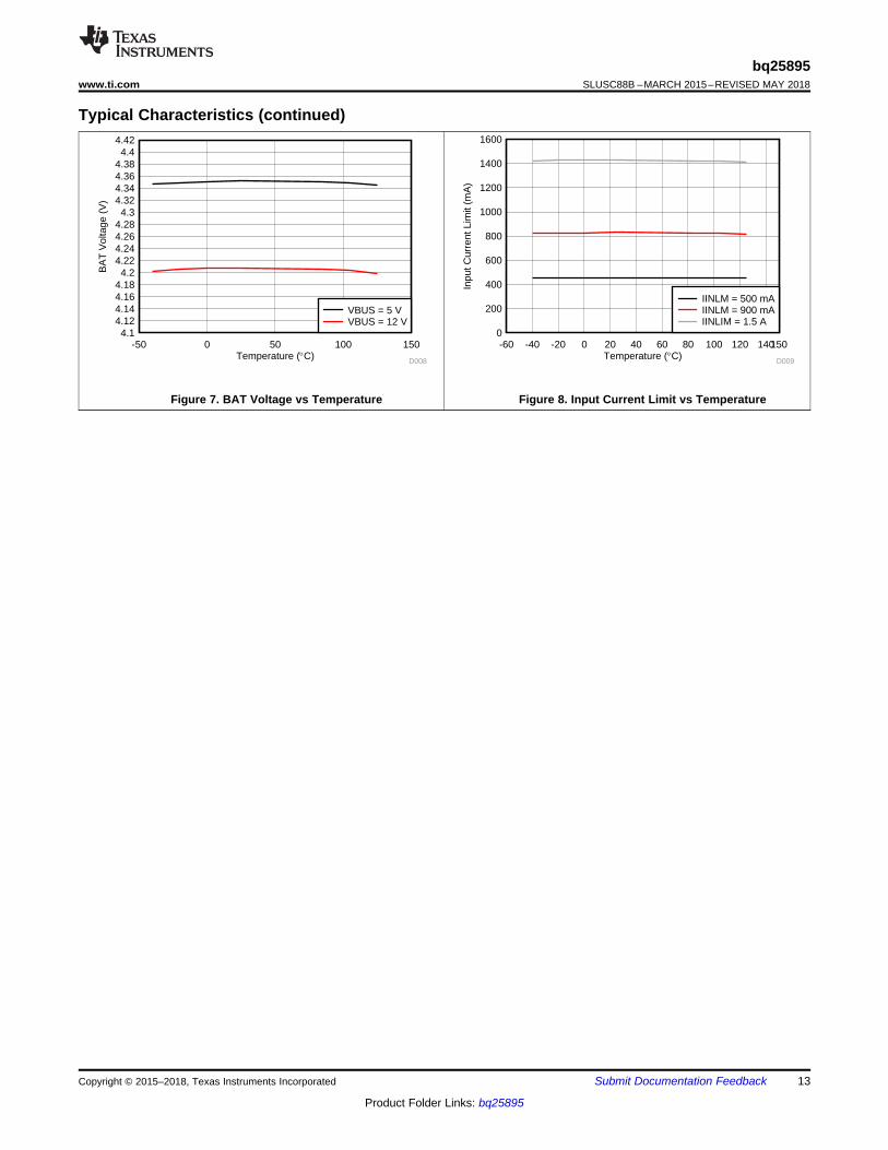
Typical Characteristics (continued)
Figure 7. BAT Voltage vs Temperature Figure 8. Input Current Limit vs Temperature

STAT
SCL SDA
FBO
CONVERTERCONTROL
PGND
REGN
BTST
REGN
TSHUT TSHUT
IC TJ
REGNLDO
bq25895
PMIDRBFET
(Q1)
VBUS
LSFET (Q3)
HSFET (Q2)SW
BATFET
(Q4)
SYS
BAT
CHARGECONTROL
STATEMACHINE
I2CInterface
INT
I INDPM
ICHG_REG
VSYSMIN
V BAT_REG
IC TJ
TREG
BATLOWVBAT
V BATLOWV
SUSPEND
RECHRGBAT
REFRESHV BTST_REFRESH
V BTST
UCPI LSFET_UCP
IQ3
BATOVP104%xVBAT_REG
BAT
VINDPM
D+
D±
Input Source
Detection
OTG
EN_CHARGEEN_BOOST
BAD_SRCIBADSRC
IDC
BAT_GDVBATGD
BAT
EN_HIZ
USBAdapter
TERMINATIONITERM
ICHG
BATSHORTBAT
V SHORT
Q2_OCPI HSFET_OCP
IQ2SYS
BAT
REFDAC
I
CHG_REG
VVBUS_UVLOZUVLO
VBATZ +80mVSLEEP
VACOVACOV
EN_HIZ
CE
ILIM
TS
ICHG
V
BAT_REGQ4 Gate Control
Q3_OCP_BOOST
Q2_UCP_BOOST
VBUS_OVP_BOOST
Battery Sensing
Thermistor
Q1 Gate Control
/QON
ADC Control
ADC
ICHG
VBUSBATSYSTS
VQON
DSEL
IQ3
IQ2
VBUS
V OTG_OVP
VOTG_HSZCP
VOTG_BAT
Converter Control State
Machine
VREG -VRECHG
-VSW
14
bq25895SLUSC88B –MARCH 2015–REVISED MAY 2018 www.ti.com
Product Folder Links: bq25895
Submit Documentation Feedback Copyright © 2015–2018, Texas Instruments Incorporated
8 Detailed DescriptionThe device is a highly integrated 5-A siwtch-mode battery charger for single cell Li-Ion and Li-polymer battery. Itis highly integrated with the input reverse-blocking FET (RBFET, Q1), high-side siwtching FET (HSFET, Q2) ,low-side switching FET (LSFET, Q3), and battery FET (BATFET, Q4). The device also integrates the boostrapdiode for the high-side gate drive.
8.1 Functional Block Diagram

15
bq25895www.ti.com SLUSC88B –MARCH 2015–REVISED MAY 2018
Product Folder Links: bq25895
Submit Documentation FeedbackCopyright © 2015–2018, Texas Instruments Incorporated
8.2 Feature Description
8.2.1 Device Power-On-Reset (POR)The internal bias circuits are powered from the higher voltage of VBUS and BAT. When VBUS rises aboveVVBUS_UVLOZ or BAT rises above VBAT_UVLOZ , the sleep comparator, battery depletion comparator and BATFETdriver are active. I2C interface is ready for communication and all the registers are reset to default value. Thehost can access all the registers after POR.
8.2.2 Device Power Up from Battery without Input SourceIf only battery is present and the voltage is above depletion threshold (VBAT_DPLZ), the BATFET turns on andconnects battery to system. The REGN LDO stays off to minimize the quiescent current. The low RDS(ON) ofBATFET and the low quiescent current on BAT minimize the conduction loss and maximize the battery run time.The device always monitors the discharge current through BATFET (Supplement Mode). When the system isoverloaded or shorted (IBAT > IBATFET_OCP), the device turns off BATFET immediately and set BATFET_DIS bit toindicate BATFET is disabled until the input source plugs in again or one of the methods describe in BATFETEnable (Exit Shipping Mode) is applied to re-enable BATFET.
8.2.3 Device Power Up from Input SourceWhen an input source is plugged in, the device checks the input source voltage to turn on REGN LDO and all thebias circuits. It detects and sets the input current limit before the buck converter is started whenAUTO_DPDM_EN bit is set. The power up sequence from input source is as listed:1. Power Up REGN LDO2. Poor Source Qualification3. Input Source Type Detection based on D+/D- to set default Input Current Limit (IINLIM) register and input
source type4. Input Voltage Limit Threshold Setting (VINDPM threshold)5. Converter Power-up
8.2.3.1 Power Up REGN Regulation (LDO)The REGN LDO supplies internal bias circuits as well as the HSFET and LSFET gate drive. The LDO alsoprovides bias rail to TS external resistors. The pull-up rail of STAT can be connected to REGN as well. TheREGN is enabled when all the below conditions are valid.1. VBUS above VVBUS_UVLOZ
2. VBUS above VBAT + VSLEEPZ in buck mode or VBUS below VBAT + VSLEEP in boost mode3. After 220 ms delay is completed
If one of the above conditions is not valid, the device is in high impedance mode (HIZ) with REGN LDO off. Thedevice draws less than IVBUS_HIZ from VBUS during HIZ state. The battery powers up the system when the deviceis in HIZ.
8.2.3.2 Poor Source QualificationAfter REGN LDO powers up, the device checks the current capability of the input source. The input source hasto meet the following requirements in order to start the buck converter.1. VBUS voltage below VACOV
2. VBUS voltage above VVBUSMIN when pulling IBADSRC (typical 30mA)
Once the input source passes all the conditions above, the status register bit VBUS_GD is set high and the INTpin is pulsed to signal to the host. If the device fails the poor source detection, it repeats poor source qualificationevery 2 seconds.

Non-Standard Adapter
DCP(3.25A)
SDP(USB100/USB500)(500mA)
CDP(1.5A)
Adapter Plug-inor
EN_DPDM
Ajustable High Voltage Adapter Handshake
0D[&KDUJH$SDSWHU
(1.5A)
USB BC1.2 Detection
Non-Standard Adapter (Divider 1: 2.1A) (Divider 2: 2A) (Divider 3: 1A)
(Divider 4: 2.4A)
16
bq25895SLUSC88B –MARCH 2015–REVISED MAY 2018 www.ti.com
Product Folder Links: bq25895
Submit Documentation Feedback Copyright © 2015–2018, Texas Instruments Incorporated
Feature Description (continued)8.2.3.3 Input Source Type DetectionAfter the VBUS_GD bit is set and REGN LDO is powered, the charger device runs Input Source Type Detectionwhen AUTO_DPDM_EN bit is set.
The bq25895 follows the USB Battery Charging Specification 1.2 (BC1.2) and to detect input source(SDP/CDP/DCP) and non-standard adapter through USB D+/D- lines. In addition, when USB DCP is detected, itinitiates adjustable high voltage adapter handshake on D+/D-. The device supports MaxCharge™ handshakewhen MAXC_EN or HVDCP_EN is set.
After input source type detection, an INT pulse is asserted to the host. In addition, the following registers and pinare changed:1. Input Current Limit (IINLIM) register is changed to set current limit2. PG_STAT bit is set3. SDP_STAT bit is updated to indicate USB100 or other input source
The host can over-write IINLIM register to change the input current limit if needed. The charger input current isalways limited by the lower of IINLIM register or ILIM pin at all-time regardless of Input Current Optimizer (ICO) isenable or disabled.
When AUTO_DPDM_EN is disabled, the Input Source Type Detection is bypassed. The Input Current Limit(IINLIM) register, VBUS_STAT, and SPD_STAT bits are unchanged from previous values.
8.2.3.3.1 D+/D– Detection Sets Input Current Limit
The bq25890 contains a D+/D– based input source detection to set the input current limit automatically. TheD+/D- detection includes standard USB BC1.2, non-standard adapter, and adjustable high voltage adapterdetections. When input source is plugged-in, the device starts standard USB BC1.2 detections. The USB BC1.2is capable to identify Standard Downstream Port (SDP), Charging Downstream Port (CDP), and DedicatedCharging Port (DCP). When the Data Contact Detection (DCD) timer of 500ms is expired, the non-standardadapter detection is applied to set the input current limit.
When DCP is detected, the device initates adjustable high voltage adapter handshake including MaxCharge™,etc. The handshake connects combinations of voltage source(s) and/or current sink on D+/D- to signal inputsource to raise output voltage from 5 V to 9 V / 12 V. The adjustable high voltage adapter handshake can bedisabled by clearing MAXC_EN and/or HVDCP_EN bits .
Figure 9. USB D+/D- Detection

17
bq25895www.ti.com SLUSC88B –MARCH 2015–REVISED MAY 2018
Product Folder Links: bq25895
Submit Documentation FeedbackCopyright © 2015–2018, Texas Instruments Incorporated
Table 1. Non-Standard Adapter DetectionNON-STANDARD
ADAPTER D+ THRESHOLD D- THRESHOLD INPUT CURRENT LIMIT
Divider 1 VD+ within V2P7_VTH VD- within V2P0_VTH 2.1ADivider 2 VD+ within V1P2_VTH VD- within V1P2_VTH 2ADivider 3 VD+ within V2P0_VTH VD- within V2P7_VTH 1ADivider 4 VD+ within V2P7_VTH VD- within V2P7_VTH 2.4A
Table 2. Adjustable High Voltage Adapter D+/D- Output ConfigurationsADJUSTABLE HIGH VOLTAGE HANDSHAKE D+ D- OUTPUT
MaxCharge (12V) I1P6MA_ISINK V3p45_VSRC 12 VMaxCharge (9V) V3p45_VSRC I1P6MA_ISINK 9 V
After the Input Source Type Detection is done, an INT pulse is asserted to the host. In addition, the followingregisters including Input Current Limit register (IINLIM), VBUS_STAT, and SDP_STAT are updated as below:
Table 3. bq25895 Result
D+/D- DETECTION INPUT CURRENT LIMIT(IINLIM) SDP_STAT VBUS_STAT
USB SDP (USB500) 500 mA 1 001USB CDP 1.5 A 1 010USB DCP 3.25 A 1 011Divider 3 1 A 1 110Divider 1 2.1 A 1 110Divider 4 2.4 A 1 110Divider 2 2 A 1 110
MaxCharge 1.5 A 1 100Unknown Adapter 500 mA 1 101

18
bq25895SLUSC88B –MARCH 2015–REVISED MAY 2018 www.ti.com
Product Folder Links: bq25895
Submit Documentation Feedback Copyright © 2015–2018, Texas Instruments Incorporated
8.2.3.3.2 Force Input Current Limit Detection
In host mode, the host can force the device to run by setting FORCE_DPDM bit. After the detection is completed,FORCE_DPDM bit returns to 0 by itself and Input Result is updated.
8.2.3.4 Input Voltage Limit Threshold Setting (VINDPM Threshold)The device supports wide range of input voltage limit (3.9 V – 14 V) for high voltage charging and provides twomethods to set Input Voltage Limit (VINDPM) threshold to facilitate autonomous detection.1. Absolute VINDPM (FORCE_VINDPM=1)
By setting FORCE_VINDPM bit to 1, the VINDPM threshold setting algorithm is disabled. Register VINDPMis writable and allows host to set the absolute threshold of VINDPM function.
2. Relative VINDPM based on VINDPM_OS registers (FORCE_VINDPM=0) (Default)
When FORCE_VINDPM bit is 0 (default), the VINDPM threshold setting algorithm is enabled. The VINDPMregister is read only and the charger controls the register by using VINDPM Threshold setting algorithm. Thealgorithm allows a wide range of adapter (VVBUS_OP) to be used with flexible VINDPM threshold.
After Input Voltage Limit Threshold is set, an INT pulse is generated to signal to the host.
8.2.3.5 Converter Power-UpAfter the input current limit is set, the converter is enabled and the HSFET and LSFET start switching. If batterycharging is disabled, BATFET turns off. Otherwise, BATFET stays on to charge the battery.
The device provides soft-start when system rail is ramped up. When the system rail is below 2.2 V, the inputcurrent limit is forced to the lower of 200 mA or IINLIM register setting. After the system rises above 2.2 V, thedevice limits input current to the lower value of ILIM pin and IILIM register (ICO_EN = 0) or IDPM_LIM register(ICO_EN = 1).
As a battery charger, the device deploys a highly efficient 1.5 MHz step-down switching regulator. The fixedfrequency oscillator keeps tight control of the switching frequency under all conditions of input voltage, batteryvoltage, charge current and temperature, simplifying output filter design.
A type III compensation network allows using ceramic capacitors at the output of the converter. An internal saw-tooth ramp is compared to the internal error control signal to vary the duty cycle of the converter. The rampheight is proportional to the PMID voltage to cancel out any loop gain variation due to a change in input voltage.
In order to improve light-load efficiency, the device switches to PFM control at light load when battery is belowminimum system voltage setting or charging is disabled. During the PFM operation, the switching duty cycle isset by the ratio of SYS and VBUS.
8.2.4 Input Current Optimizer (ICO)The device provides innovative Input Current Optimizer (ICO) to identify maximum power point without overloadthe input source. The algorithm automatically identify maximum input current limit of power source withoutentering VINDPM to avoid input source overload.
This feature is enabled by default (ICO_EN=1) and can be disabled by setting ICO_EN bit to 0. After DCP orMaxCharge type input source is detected based on the procedures previously described (Input Source TypeDetection ). The algorithm runs automatically when ICO_EN bit is set. The algorithm can also be forced toexecute by setting FORCE_ICO bit regardless of input source type detected.
The actual input current limit used by the Dynamic Power Management is reported in IDPM_LIM register whileInput Current Optimizer is enabled (ICO_EN = 1) or set by IINLIM register when the algorithm is disabled(ICO_EN = 0). In addition, the current limit is clamped by ILIM pin unless EN_ILIM bit is 0 to disable ILIM pinfunction.

BAT (V)
Sys
tem
Vol
tage
(V
)
2.7 2.9 3.1 3.3 3.5 3.7 3.9 4.1 4.33.4
3.6
3.8
4
4.2
4.4
D011
Minimum System VoltageSYS (Charge Disabled)SYS (Charge Enabled)
19
bq25895www.ti.com SLUSC88B –MARCH 2015–REVISED MAY 2018
Product Folder Links: bq25895
Submit Documentation FeedbackCopyright © 2015–2018, Texas Instruments Incorporated
8.2.5 Boost Mode Operation from BatteryThe device supports boost converter operation to deliver power from the battery to other portable devicesthrough PMID pin. The boost mode output current rating supports maximum output current up to 3.1 A to chargesmartphone and tablet at fast charging rate. The boost operation can be enabled if the conditions are valid:1. BAT above BATLOWV
2. VBUS less than BAT+VSLEEP (in sleep mode)3. Boost mode operation is enabled (OTG pin HIGH and OTG_CONFIG bit =1)4. Voltage at TS (thermistor) pin is within range configured by Boost Mode Temperature Monitor as configured
by BHOT and BCOLD bits5. After 30 ms delay from boost mode enable
In boost mode, the device employs a 500 KHz or 1.5 MHz (selectable using BOOST_FREQ bit) step-upswitching regulator based on system requirements. To avoid frequency change during boost mode operations,write to boost frequency configuration bit (BOOST_FREQ) is ignored when OTG_CONFIG is set.
During boost mode, the status register VBUS_STAT bits is set to 111, the VBUS output is 5V by default(selectable via BOOSTV register bits). The boost output is maintained when BAT is above VOTG_BAT threshold
8.2.6 Power Path ManagementThe device accommodates a wide range of input sources from USB, wall adapter, to car battery. The deviceprovides automatic power path selection to supply the system (SYS) from input source (VBUS), battery (BAT), orboth.
8.2.6.1 Narrow VDC ArchitectureThe device deploys Narrow VDC architecture (NVDC) with BATFET separating system from battery. Theminimum system voltage is set by SYS_MIN bits. Even with a fully depleted battery, the system is regulatedabove the minimum system voltage (default 3.5 V).
When the battery is below minimum system voltage setting, the BATFET operates in linear mode (LDO mode),and the system is regulated above the minimum system voltage setting. As the battery voltage rises above theminimum system voltage, BATFET is fully on and the voltage difference between the system and battery is theVDS of BATFET. The status register VSYS_STAT bit goes high when the system is in minimum system voltageregulation.
Figure 10. V(SYS) vs V(BAT)
8.2.6.2 Dynamic Power ManagementTo meet maximum current limit in USB spec and avoid over loading the adapter, the device features DynamicPower Management (DPM), which continuously monitors the input current and input voltage. When input sourceis over-loaded, either the current exceeds the input current limit (IINLIM or IDPM_LIM) or the voltage falls belowthe input voltage limit (VINDPM). The device then reduces the charge current until the input current falls belowthe input current limit and the input voltage rises above the input voltage limit.

V(BAT_SYS) (mV)
Cur
rent
(A
)
0 5 10 15 20 25 30 35 40 45 50 550.0
0.5
1.0
1.5
2.0
2.5
3.0
3.5
4.0
4.5
5.0
D010
2.8A
4A
-0.6A
3.2A
0.5A
3.6V3.4V3.2V
3.18V
1.2A1.0A
DPM DPMSupplement
SYS
VBUS
BAT
ICHG
IIN
ISYS
Current
Voltage
20
bq25895SLUSC88B –MARCH 2015–REVISED MAY 2018 www.ti.com
Product Folder Links: bq25895
Submit Documentation Feedback Copyright © 2015–2018, Texas Instruments Incorporated
When the charge current is reduced to zero, but the input source is still overloaded, the system voltage starts todrop. Once the system voltage falls below the battery voltage, the device automatically enters the SupplementMode where the BATFET turns on and battery starts discharging so that the system is supported from both theinput source and battery.
During DPM mode, the status register bits VDPM_STAT (VINDPM) and/or IDPM_STAT (IINDPM) is/are set high.Figure 11 shows the DPM response with 9V/1.2A adapter, 3.2-V battery, 2.8-A charge current and 3.4-Vminimum system voltage setting.
Figure 11. DPM Response
8.2.6.3 Supplement ModeWhen the system voltage falls below the battery voltage, the BATFET turns on and the BATFET gate isregulated the gate drive of BATFET so that the minimum BATFET VDS stays at 30 mV when the current is low.This prevents oscillation from entering and exiting the Supplement Mode. As the discharge current increases, theBATFET gate is regulated with a higher voltage to reduce RDS(ON) until the BATFET is in full conduction. At thispoint onwards, the BATFET VDS linearly increases with discharge current. Figure 12 shows the V-I curve of theBATFET gate regulation operation. BATFET turns off to exit Supplement Mode when the battery is below batterydepletion threshold.
Figure 12. BATFET V-I Curve

21
bq25895www.ti.com SLUSC88B –MARCH 2015–REVISED MAY 2018
Product Folder Links: bq25895
Submit Documentation FeedbackCopyright © 2015–2018, Texas Instruments Incorporated
8.2.7 Battery Charging ManagementThe device charges 1-cell Li-Ion battery with up to 5-A charge current for high capacity battery. The 11-mΩBATFET improves charging efficiency and minimize the voltage drop during discharging.
8.2.7.1 Autonomous Charging CycleWith battery charging is enabled (CHG_CONFIG bit = 1 and CE pin is low), the device autonomously completesa charging cycle without host involvement. The device default charging parameters are listed in Table 4. Thehost can always control the charging operations and optimize the charging parameters by writing to thecorresponding registers through I2C.
Table 4. Charging Parameter Default SettingDEFAULT MODE bq25895Charging Voltage 4.208 VCharging Current 2.048 A
Pre-charge Current 128 mATermination Current 256 mATemperature Profile Cold/Hot
Safety Timer 12 hour
A new charge cycle starts when the following conditions are valid:• Converter starts• Battery charging is enabled by setting CHG_CONFIG bit, /CE pin is low and ICHG register is not 0 mA• No thermistor fault on TS pin• No safety timer fault• BATFET is not forced to turn off (BATFET_DIS bit = 0)
The charger device automatically terminates the charging cycle when the charging current is below terminationthreshold, charge voltage is above recharge threshold, and device not in DPM mode or thermal regulation. Whena full battery voltage is discharged below recharge threshold (threshold selectable via VRECHG bit), the deviceautomatically starts a new charging cycle. After the charge is done, either toggle CE pin or CHG_CONFIG bitcan initiate a new charging cycle.
The STAT output indicates the charging status of charging (LOW), charging complete or charge disable (HIGH)or charging fault (Blinking). The STAT output can be disabled by setting STAT_DIS bit. In addition, the statusregister (CHRG_STAT) indicates the different charging phases: 00-charging disable, 01-precharge, 10-fastcharge (constant current) and constant voltage mode, 11-charging done. Once a charging cycle is completed, anINT is asserted to notify the host.
8.2.7.2 Battery Charging ProfileThe device charges the battery in three phases: preconditioning, constant current and constant voltage. At thebeginning of a charging cycle, the device checks the battery voltage and regulates current / voltage.
Table 5. Charging Current SettingVBAT CHARGING CURRENT REG DEFAULT SETTING CHRG_STAT< 2 V IBATSHORT – 01
2 V – 3 V IPRECHG 128 mA 01> 3 V ICHG 2048 mA 10
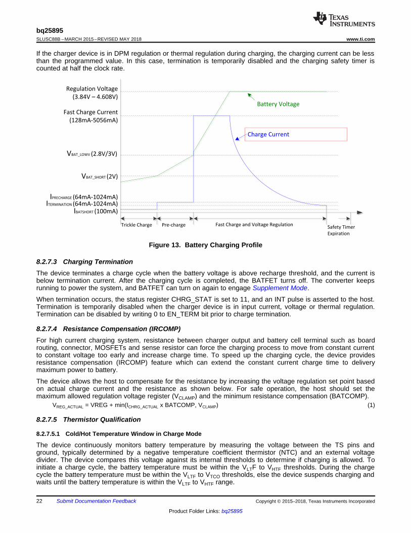
Regulation Voltage
(3.84V t 4.608V)
Fast Charge Current
(128mA-5056mA)
VBAT_LOWV (2.8V/3V)
VBAT_SHORT (2V)
IPRECHARGE (64mA-1024mA)ITERMINATION (64mA-1024mA)
IBATSHORT (100mA)
Battery Voltage
Charge Current
Trickle Charge Pre-charge Fast Charge and Voltage RegulationSafety Timer
Expiration
22
bq25895SLUSC88B –MARCH 2015–REVISED MAY 2018 www.ti.com
Product Folder Links: bq25895
Submit Documentation Feedback Copyright © 2015–2018, Texas Instruments Incorporated
If the charger device is in DPM regulation or thermal regulation during charging, the charging current can be lessthan the programmed value. In this case, termination is temporarily disabled and the charging safety timer iscounted at half the clock rate.
Figure 13. Battery Charging Profile
8.2.7.3 Charging TerminationThe device terminates a charge cycle when the battery voltage is above recharge threshold, and the current isbelow termination current. After the charging cycle is completed, the BATFET turns off. The converter keepsrunning to power the system, and BATFET can turn on again to engage Supplement Mode.
When termination occurs, the status register CHRG_STAT is set to 11, and an INT pulse is asserted to the host.Termination is temporarily disabled when the charger device is in input current, voltage or thermal regulation.Termination can be disabled by writing 0 to EN_TERM bit prior to charge termination.
8.2.7.4 Resistance Compensation (IRCOMP)For high current charging system, resistance between charger output and battery cell terminal such as boardrouting, connector, MOSFETs and sense resistor can force the charging process to move from constant currentto constant voltage too early and increase charge time. To speed up the charging cycle, the device providesresistance compensation (IRCOMP) feature which can extend the constant current charge time to deliverymaximum power to battery.
The device allows the host to compensate for the resistance by increasing the voltage regulation set point basedon actual charge current and the resistance as shown below. For safe operation, the host should set themaximum allowed regulation voltage register (VCLAMP) and the minimum resistance compensation (BATCOMP).
VREG_ACTUAL = VREG + min(ICHRG_ACTUAL x BATCOMP, VCLAMP) (1)
8.2.7.5 Thermistor Qualification
8.2.7.5.1 Cold/Hot Temperature Window in Charge Mode
The device continuously monitors battery temperature by measuring the voltage between the TS pins andground, typically determined by a negative temperature coefficient thermistor (NTC) and an external voltagedivider. The device compares this voltage against its internal thresholds to determine if charging is allowed. Toinitiate a charge cycle, the battery temperature must be within the VLTF to VHTF thresholds. During the chargecycle the battery temperature must be within the VLTF to VTCO thresholds, else the device suspends charging andwaits until the battery temperature is within the VLTF to VHTF range.

REGN COLD HOT
REGN REGNHOT COLD
REGN
COLD
1 1V RTH RTH
VT1 VT5 RT2
V VRTH 1 RTH 1
VT5 VT1
V1
VT1RT1
1 1
RT2 RTH
æ ö´ ´ ´ -ç ÷
è ø=æ ö æ ö
´ - - ´ -ç ÷ ç ÷è ø è ø
-=
+
TEMPERATURE RANGE TO
INITIATE CHARGE
TEMPERATURE RANGE
DURING A CHARGE CYCLE
CHARGE SUSPENDED CHARGE SUSPENDED
V VREF
VLTF
CHARGE at full C CHARGE at full C
VHTF
VTCO
CHARGE SUSPENDEDCHARGE SUSPENDED
AGND AGND
VLTFH VLTFH
VLTF
REGN
REGN
TS
RT2
RT1
RTH
103AT
bq25895
23
bq25895www.ti.com SLUSC88B –MARCH 2015–REVISED MAY 2018
Product Folder Links: bq25895
Submit Documentation FeedbackCopyright © 2015–2018, Texas Instruments Incorporated
Figure 14. TS Resistor Network
When the TS fault occurs, the fault register REG0C[2:0] indicates the actual condition on each TS pin and an INTis asserted to the host. The STAT pin indicates the fault when charging is suspended.
Figure 15. TS Pin Thermistor Sense Thresholds
Assuming a 103AT NTC thermistor on the battery pack as shown in Figure 14, the value RT1 and RT2 can bedetermined by using Equation 2: :
(2)
Select 0°C to 45°C range for Li-ion or Li-polymer battery,RTHCOLD = 27.28 kΩRTHHOT = 4.91 kΩRT1 = 5.21 kΩRT2 = 29.87 kΩ

Temperature Range toBoost
Boost Disable
VREGN
V BCOLDx
( -10ºC / 20ºC)
Boost Enable
VBHOTx
(55ºC / 60ºC / 65ºC)
Boost Disable
AGND
24
bq25895SLUSC88B –MARCH 2015–REVISED MAY 2018 www.ti.com
Product Folder Links: bq25895
Submit Documentation Feedback Copyright © 2015–2018, Texas Instruments Incorporated
8.2.7.5.2 Cold/Hot Temperature Window in Boost Mode
For battery protection during boost mode, the device monitors the battery temperature to be within the VBCOLDx toVBHOTx thresholds unless boost mode temperature is disabled by setting BHOT bits to 11. When temperature isoutside of the temperature thresholds, the boost mode and BATFET are disabled and BATFET_DIS bit is set toreduce leakage current on PMID. Once temperature returns within thresholds, the host can clear BATFET_DISbit or provide logic low to high transition on QON pin to enable BATFET and boost mode.
Figure 16. TS Pin Thermistor Sense Thresholds in Boost Mode
8.2.7.6 Charging Safety TimerThe device has built-in safety timer to prevent extended charging cycle due to abnormal battery conditions. Thesafety timer is 4 hours when the battery is below VBATLOWV threshold. The user can program fast charge safetytimer through I2C (CHG_TIMER bits). When safety timer expires, the fault register CHRG_FAULT bits are set to11 and an INT is asserted to the host. The safety timer feature can be disabled via I2C by setting EN_TIMER bit.
During input voltage, current or thermal regulation, the safety timer counts at half clock rate as the actual chargecurrent is likely to be below the register setting. For example, if the charger is in input current regulation(IDPM_STAT = 1) throughout the whole charging cycle, and the safety time is set to 5 hours, the safety timer willexpire in 10 hours. This half clock rate feature can be disabled by writing 0 to TMR2X_EN bit.
8.2.8 Battery MonitorThe device includes a battery monitor to provide measurements of VBUS voltage, battery voltage, systemvoltage, thermistor ratio, and charging current, and charging current based on the device modes of operation.The measurements are reported in Battery Monitor Registers (REG0E-REG12). The battery monitor can beconfigured as two conversion modes by using CONV_RATE bit: one-shot conversion (default) and 1 secondcontinuous conversion.
For one-shot conversion (CONV_RATE = 0), the CONV_START bit can be set to start the conversion. During theconversion, the CONV_START is set and it is cleared by the device when conversion is completed. Theconversion result is ready after tCONV (maximum 1 second).
For continuous conversion (CONV_RATE = 1), the CONV_RATE bit can be set to initiate the conversion. Duringactive conversion, the CONV_START is set to indicate conversion is in progress. The battery monitor providesconversion result every 1 second automatically. The battery monitor exits continuous conversion mode whenCONV_RATE is cleared.
When battery monitor is active, the REGN power is enabled and can increase device quiescent current. Inbattery only mode, the battery monitor is only active when V(BAT) > SYS_MIN setting in REG03.

25
bq25895www.ti.com SLUSC88B –MARCH 2015–REVISED MAY 2018
Product Folder Links: bq25895
Submit Documentation FeedbackCopyright © 2015–2018, Texas Instruments Incorporated
Table 6. Battery Monitor Modes of Operation
PARAMETER REGISTERMODES OF OPERATION
CHARGEMODE BOOST MODE DISABLE CHARGE
MODEBATTERY ONLY
MODEBattery Voltage (VBAT) REG0E Yes Yes Yes YesSystem Voltage (VSYS) REG0F Yes Yes Yes Yes
Temperature (TS) Voltage (VTS) REG10 Yes Yes Yes YesVBUS Voltage (VVBUS) REG11 Yes Yes Yes NACharge Current (IBAT) REG12 Yes NA NA NA
8.2.9 Status Outputs (STAT, and INT)
8.2.9.1 Charging Status Indicator (STAT)The device indicates charging state on the open drain STAT pin. The STAT pin can drive LED as shown inFigure 47. The STAT pin function can be disable by setting STAT_DIS bit.
Table 7. STAT Pin StateCHARGING STATE STAT INDICATOR
Charging in progress (including recharge) LOWCharging complete HIGHSleep mode, charge disable HIGHCharge suspend (Input overvoltage, TS fault, timer fault, input or system overvoltage).Boost Mode suspend (due to TS Fault) blinking at 1 Hz
8.2.9.2 Interrupt to Host (INT)In some applications, the host does not always monitor the charger operation. The INT notifies the system on thedevice operation. The following events will generate 256-µs INT pulse.• USB/adapter source identified (through PSEL or DPDM detection, with OTG pin)• Good input source detected
– VBUS above battery (not in sleep)– VBUS below VACOV threshold– VBUS above VVBUSMIN (typical 3.8 V) when IBADSRC (typical 30 mA) current is applied (not a poor source)
• Input removed• Charge Complete• Any FAULT event in REG0C
When a fault occurs, the charger device sends out INT and keeps the fault state in REG0C until the host readsthe fault register. Before the host reads REG0C and all the faults are cleared, the charger device would not sendany INT upon new faults. To read the current fault status, the host has to read REG0C two times consecutively.The 1st read reports the pre-existing fault register status and the 2nd read reports the current fault register status.
8.2.10 BATET (Q4) Control
8.2.10.1 BATFET Disable Mode (Shipping Mode)To extend battery life and minimize power when system is powered off during system idle, shipping, or storage,the device can turn off BATFET so that the system voltage is zero to minimize the battery leakage current. Whenthe host set BATFET_DIS bit, the charger can turn off BATFET immediately or delay by tSM_DLY as configuratedby BATFET_DLY bit.
8.2.10.2 BATFET Enable (Exit Shipping Mode)When the BATFET is disabled (in shipping mode) and indicated by setting BATFET_DIS, one of the followingevents can enable BATFET to restore system power:1. Plug in adapter

ILIM ILIMIN
ILIM
K x VI =
R x 0.8 V
ILIMINMAX
ILIM
KI =
R
26
bq25895SLUSC88B –MARCH 2015–REVISED MAY 2018 www.ti.com
Product Folder Links: bq25895
Submit Documentation Feedback Copyright © 2015–2018, Texas Instruments Incorporated
2. Clear BATFET_DIS bit3. Set REG_RST bit to reset all registers including BATFET_DIS bit to default (0)4. A logic high to low transition on QON pin with tSHIPMODE deglitch time to enable BATFET to exit shipping
mode
8.2.10.3 BATFET Full System ResetThe BATFET functions as a load switch between battery and system when input source is not plugged-in. Bychanging the state of BATFET from off to on, system connects to SYS can be effectively have a power-on-reset.The QON pin supports push-button interface to reset system power without host by change the state of BATFET.
When the QON pin is driven to logic low for tQON_RST (typical 15 seconds) while input source is not plugged inand BATFET is enabled (BATFET_DIS=0), the BATFET is turned off for tBATFET_RST and then it is re-enabled toreset system power. This function can be disabled by setting BATFET_RST_EN bit to 0.
8.2.11 Current Pulse Control ProtocolThe device provides the control to generate the VBUS current pulse protocol to communicate with adjustablehigh voltage adapter in order to signal adapter to increase or decrease output voltage. To enable the interface,the EN_PUMPX bit must be set. Then the host can select the increase/decrease voltage pulse by setting one ofthe PUMPX_UP or PUMPX_DN bit (but not both) to start the VBUS current pulse sequence. During the currentpulse sequence, the PUMPX_UP and PUMPX_DN bits are set to indicate pulse sequence is in progress and thedevice pulses the input current limit between current limit set forth by IINLIM or IDPM_LIM register and the100mA current limit (IINDPM100_ACC). When the pulse sequence is completed, the input current limit is returned tovalue set by IINLIM or IDPM_LIM register and the PUMPX_UP or PUMPX_DN bit is cleared. In addition, theEN_PUMPX can be cleared during the current pulse sequence to terminate the sequence and force charger toreturn to input current limit as set forth by the IINLIM or IDPM_LIM register immediately. When EN_PUMPX bit islow, write to PUMPX_UP and PUMPX_DN bit would be ignored and have no effect on VBUS current limit.
8.2.12 Input Current Limit on ILIMFor safe operation, the device has an additional hardware pin on ILIM to limit maximum input current on ILIM pin.The input maximum current is set by a resistor from ILIM pin to ground as:
(3)
The actual input current limit is the lower value between ILIM setting and register setting (IINLIM). For example, ifthe register setting is 111111 for 3.25 A, and ILIM has a 260-Ω resistor (KILIM = 390 max.) to ground for 1.5 A,the input current limit is 1.5 A. ILIM pin can be used to set the input current limit rather than the register settingswhen EN_ILIM bit is set. The device regulates ILIM pin at 0.8 V. If ILIM voltage exceeds 0.8 V, the device entersinput current regulation (Refer to Dynamic Power Management section).
The ILIM pin can also be used to monitor input current when EN_ILIM is enabled. The voltage on ILIM pin isproportional to the input current. ILIM pin can be used to monitor the input current following Equation 4:
(4)
For example, if ILIM pin is set with 260-Ω resistor, and the ILIM voltage is 0.4 V, the actual input current 0.615 A- 0.75 A (based on KILM specified). If ILIM pin is open, the input current is limited to zero since ILIM voltagefloats above 0.8 V. If ILIM pin is short, the input current limit is set by the register.
The ILIM pin function can be disabled by setting EN_ILIM bit to 0. When the pin is disabled, both input currentlimit function and monitoring function are not available.
8.2.13 Thermal Regulation and Thermal Shutdown
8.2.13.1 Thermal Protection in Buck ModeThe device monitors the internal junction temperature TJ to avoid overheat the chip and limits the IC surfacetemperature in buck mode. When the internal junction temperature exceeds the preset thermal regulation limit(TREG bits), the device lowers down the charge current. The wide thermal regulation range from 60ºC to 120ºCallows the user to optimize the system thermal performance.

27
bq25895www.ti.com SLUSC88B –MARCH 2015–REVISED MAY 2018
Product Folder Links: bq25895
Submit Documentation FeedbackCopyright © 2015–2018, Texas Instruments Incorporated
During thermal regulation, the actual charging current is usually below the programmed battery charging current.Therefore, termination is disabled, the safety timer runs at half the clock rate, and the status registerTHERM_STAT bit goes high.
Additionally, the device has thermal shutdown to turn off the converter and BATFET when IC surfacetemperature exceeds TSHUT. The fault register CHRG_FAULT is set to 10 and an INT is asserted to the host. TheBATFET and converter is enabled to recover when IC temperature is below TSHUT_HYS.
8.2.13.2 Thermal Protection in Boost ModeThe device monitors the internal junction temperature to provide thermal shutdown during boost mode. When ICsurface temperature exceeds TSHUT, BATFET is turned off to disable battery discharge. When IC surfacetemperature is below TSHUT_HYS, the host can use one of the method describes in section BATFET Enable (ExitShipping Mode) to recover.
8.2.14 Voltage and Current Monitoring in Buck and Boost Mode
8.2.14.1 Voltage and Current Monitoring in Buck ModeThe device closely monitors the input and system voltage, as well as HSFET current for safe buck and boostmode operations.
8.2.14.1.1 Input Overvoltage (ACOV)
The input voltage for buck mode operation is VVBUS_OP. If VBUS voltage exceeds VACOV, the device stopsswitching immediately. During input over voltage (ACOV), the fault register CHRG_FAULT bits sets to 01. An INTis asserted to the host..
8.2.14.1.2 System Overvoltage Protection (SYSOVP)
The charger device clamps the system voltage during load transient so that the components connect to systemwould not be damaged due to high voltage. When SYSOVP is detected, the converter stops immediately toclamp the overshoot.
8.2.14.2 Current Monitoring in Boost ModeThe device closely monitors the VBUS voltage, as well as LSFET current to ensure safe boost mode operation.
8.2.14.2.1 Boost Mode Overvoltage Protection
When PMID voltage rises above regulation target and exceeds VOTG_OVP, the device enters overvoltageprotection which stops switching and pauses boost mode (OTG_CONFIG bit remains set) until OVP fault isremoved. During the overvoltage, the fault register bit (BOOST_FAULT) is set high to indicate fault in boostoperation. An INT is also asserted to the host.
8.2.15 Battery Protection
8.2.15.1 Battery Overvoltage Protection (BATOVP)The battery overvoltage limit is clamped at 4% above the battery regulation voltage. When battery over voltageoccurs, the charger device immediately disables charge. The fault register BAT_FAULT bit goes high and an INTis asserted to the host.
8.2.15.2 Battery Over-Discharge ProtectionWhen battery is discharged below VBAT_DPL, the BATFET is turned off to protect battery from over discharge. Torecover from over-discharge, an input source is required at VBUS. When an input source is plugged in, theBATFET turns on. Thy is charged with IBATSHORT (typically 100 mA) current when the VBAT < VSHORT, orprecharge current as set in IPRECHG register when the battery voltage is between VSHORT and VBATLOWV.
8.2.15.3 System Overcurrent ProtectionWhen the system is shorted or significantly overloaded (IBAT > IBATOP) so that its current exceeds the overcurrentlimit, the device latches off BATFET. Section BATFET Enable (Exit Shipping Mode) can reset the latch-offcondition and turn on BATFET

START (S) STOP (P)
SDA
SCL
SDA
SCL
SDA
SCL
Data line stable;
Data valid
Change
of data
allowed
28
bq25895SLUSC88B –MARCH 2015–REVISED MAY 2018 www.ti.com
Product Folder Links: bq25895
Submit Documentation Feedback Copyright © 2015–2018, Texas Instruments Incorporated
8.2.16 Serial InterfaceThe device uses I2C compatible interface for flexible charging parameter programming and instantaneous devicestatus reporting. I2C is a bi-directional 2-wire serial interface. Only two open-drain bus lines are required: a serialdata line (SDA) and a serial clock line (SCL). Devices can be considered as masters or slaves when performingdata transfers. A master is the device which initiates a data transfer on the bus and generates the clock signalsto permit that transfer. At that time, any device addressed is considered a slave.
The device operates as a slave device with address 6AH, receiving control inputs from the master device likemicro controller or a digital signal processor through REG00-REG14. Register read beyond REG14 (0x14)returns 0xFF. The I2C interface supports both standard mode (up to 100 kbits), and fast mode (up to 400 kbits).When the bus is free, both lines are HIGH. The SDA and SCL pins are open drain and must be connected to thepositive supply voltage via a current source or pull-up resistor.
8.2.16.1 Data ValidityThe data on the SDA line must be stable during the HIGH period of the clock. The HIGH or LOW state of thedata line can only change when the clock signal on the SCL line is LOW. One clock pulse is generated for eachdata bit transferred.
Figure 17. Bit Transfer on the I2C Bus
8.2.16.2 START and STOP ConditionsAll transactions begin with a START (S) and can be terminated by a STOP (P). A HIGH to LOW transition on theSDA line while SCl is HIGH defines a START condition. A LOW to HIGH transition on the SDA line when theSCL is HIGH defines a STOP condition.
START and STOP conditions are always generated by the master. The bus is considered busy after the STARTcondition, and free after the STOP condition.
Figure 18. START and STOP conditions

1 7
Slave AddressS
1 1
ACK
8
Reg Addr ACK
1
Data Addr ACK
1 1
P
8
0
SCL
SDA
START
S 1-7 8 9
ACK
1-7 8 9
ACK
1-7 8 9
STOP
P
ADDRESS R/W DATA ACKDATA
START or
Repeated
START
S or Sr 1 2 7 8 9
MSB
ACK
Acknowledgement
signal from slave
1 2 8 9ACK
STOP or
Repeated
START
P or
Sr
Acknowledgement
signal from revceiver
29
bq25895www.ti.com SLUSC88B –MARCH 2015–REVISED MAY 2018
Product Folder Links: bq25895
Submit Documentation FeedbackCopyright © 2015–2018, Texas Instruments Incorporated
8.2.16.3 Byte FormatEvery byte on the SDA line must be 8 bits long. The number of bytes to be transmitted per transfer isunrestricted. Each byte has to be followed by an Acknowledge bit. Data is transferred with the Most SignificantBit (MSB) first. If a slave cannot receive or transmit another complete byte of data until it has performed someother function, it can hold the clock line SCL low to force the master into a wait state (clock stretching). Datatransfer then continues when the slave is ready for another byte of data and release the clock line SCL.
Figure 19. Data Transfer on the I2C Bus
8.2.16.4 Acknowledge (ACK) and Not Acknowledge (NACK)The acknowledge takes place after every byte. The acknowledge bit allows the receiver to signal the transmitterthat the byte was successfully received and another byte may be sent. All clock pulses, including theacknowledge 9th clock pulse, are generated by the master.
The transmitter releases the SDA line during the acknowledge clock pulse so the receiver can pull the SDA lineLOW and it remains stable LOW during the HIGH period of this clock pulse.
When SDA remains HIGH during the 9th clock pulse, this is the Not Acknowledge signal. The master can thengenerate either a STOP to abort the transfer or a repeated START to start a new transfer.
8.2.16.5 Slave Address and Data Direction BitAfter the START, a slave address is sent. This address is 7 bits long followed by the eighth bit as a data directionbit (bit R/W). A zero indicates a transmission (WRITE) and a one indicates a request for data (READ).
Figure 20. Complete Data Transfer
8.2.16.6 Single Read and Write
Figure 21. Single Write

1 7
Slave AddressS
1 1
ACK
8
Reg Addr ACK
1
ACK
1
1
P
7
0 1
Data NCK
8
Slave Address
1
1
1
S
30
bq25895SLUSC88B –MARCH 2015–REVISED MAY 2018 www.ti.com
Product Folder Links: bq25895
Submit Documentation Feedback Copyright © 2015–2018, Texas Instruments Incorporated
Figure 22. Single Read
If the register address is not defined, the charger IC send back NACK and go back to the idle state.
8.2.16.7 Multi-Read and Multi-WriteThe charger device supports multi-read and multi-write on REG00 through REG14 except REG0C.
Figure 23. Multi-Write
Figure 24. Multi-Read
REG0C is a fault register. It keeps all the fault information from last read until the host issues a new read. Forexample, if Charge Safety Timer Expiration fault occurs but recovers later, the fault register REG0C reports thefault when it is read the first time, but returns to normal when it is read the second time. In order to get the faultinformation at present, the host has to read REG0C for the second time. The only exception is NTC_FAULTwhich always reports the actual condition on the TS pin. In addition, REG0C does not support multi-read andmulti-write.
8.3 Device Functional Modes
8.3.1 Host Mode and Default ModeThe device is a host controlled charger, but it can operate in default mode without host management. In defaultmode, the device can be used an autonomous charger with no host or while host is in sleep mode. When thecharger is in default mode, WATCHDOG_FAULT bit is HIGH. When the charger is in host mode,WATCHDOG_FAULT bit is LOW.
After power-on-reset, the device starts in default mode with watchdog timer expired, or default mode. All theregisters are in the default settings.
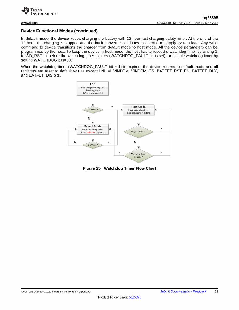
PORwatchdog timer expired
Reset registers
I2C interface enabled
I2C Write?
Host ModeStart watchdog timer
Host programs registers
Y
N
Default ModeReset watchdog timer
Reset selective registers WD_RST bit = 1? Y
N
Watchdog Timer
Expired?
I2C Write?
Y N
YN
31
bq25895www.ti.com SLUSC88B –MARCH 2015–REVISED MAY 2018
Product Folder Links: bq25895
Submit Documentation FeedbackCopyright © 2015–2018, Texas Instruments Incorporated
Device Functional Modes (continued)In default mode, the device keeps charging the battery with 12-hour fast charging safety timer. At the end of the12-hour, the charging is stopped and the buck converter continues to operate to supply system load. Any writecommand to device transitions the charger from default mode to host mode. All the device parameters can beprogrammed by the host. To keep the device in host mode, the host has to reset the watchdog timer by writing 1to WD_RST bit before the watchdog timer expires (WATCHDOG_FAULT bit is set), or disable watchdog timer bysetting WATCHDOG bits=00.
When the watchdog timer (WATCHDOG_FAULT bit = 1) is expired, the device returns to default mode and allregisters are reset to default values except IINLIM, VINDPM, VINDPM_OS, BATFET_RST_EN, BATFET_DLY,and BATFET_DIS bits.
Figure 25. Watchdog Timer Flow Chart

32
bq25895SLUSC88B –MARCH 2015–REVISED MAY 2018 www.ti.com
Product Folder Links: bq25895
Submit Documentation Feedback Copyright © 2015–2018, Texas Instruments Incorporated
8.4 Register MapsI2C Slave Address: 6AH (1101010B + R/W)
8.4.1 REG00
Figure 26. REG00
7 6 5 4 3 2 1 00 0 0 0 1 0 0 0
R/W R/W R/W R/W R/W R/W R/W R/WLEGEND: R/W = Read/Write; R = Read only; -n = value after reset
Table 8. REG00Bit Field Type Reset Description
7 EN_HIZ R/W by REG_RSTby Watchdog
Enable HIZ Mode0 – Disable (default)1 – Enable
6 EN_ILIM R/W by REG_RSTby Watchdog
Enable ILIM Pin0 – Disable1 – Enable (default: Enable ILIM pin (1))
5 IINLIM[5] R/W by REG_RST 1600mA Input Current LimitOffset: 100mARange: 100mA (000000) – 3.25A (111111)Default:0001000 (500mA)(Actual input current limit is the lower of I2C or ILIM pin)IINLIM bits are changed automaticallly after input sourcetype detection is completedUSB Host SDP w/ OTG=Hi (USB500) = 500mAUSB Host SDP w/ OTG=Lo (USB100) = 500mAUSB CDP = 1.5AUSB DCP = 3.25AAdjustable High Voltage (MaxCharge) DCP = 1.5AUnknown Adapter = 500mANon-Standard Adapter = 1A/2A/2.1A/2.4A
4 IINLIM[4] R/W by REG_RST 800mA
3 IINLIM[3] R/W by REG_RST 400mA
2 IINLIM[2] R/W by REG_RST 200mA
1 IINLIM[1] R/W by REG_RST 100mA
0 IINLIM[0] R/W by REG_RST 50mA
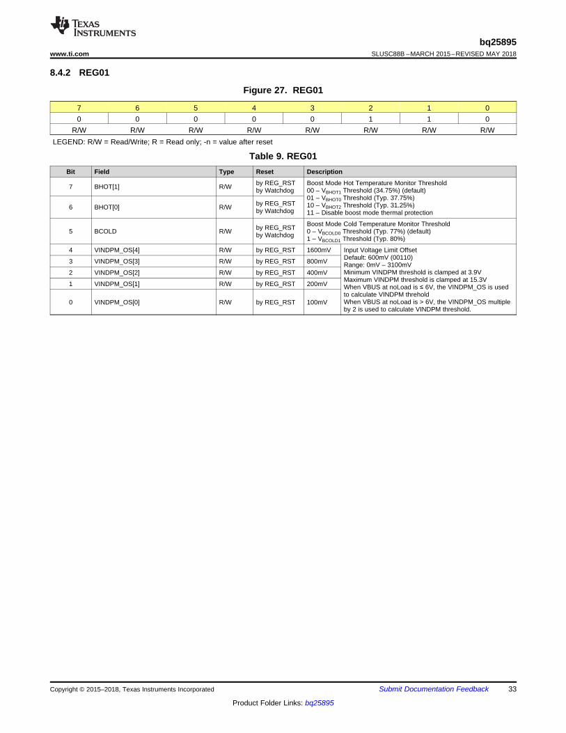
33
bq25895www.ti.com SLUSC88B –MARCH 2015–REVISED MAY 2018
Product Folder Links: bq25895
Submit Documentation FeedbackCopyright © 2015–2018, Texas Instruments Incorporated
8.4.2 REG01
Figure 27. REG01
7 6 5 4 3 2 1 00 0 0 0 0 1 1 0
R/W R/W R/W R/W R/W R/W R/W R/WLEGEND: R/W = Read/Write; R = Read only; -n = value after reset
Table 9. REG01Bit Field Type Reset Description
7 BHOT[1] R/W by REG_RSTby Watchdog
Boost Mode Hot Temperature Monitor Threshold00 – VBHOT1 Threshold (34.75%) (default)01 – VBHOT0 Threshold (Typ. 37.75%)10 – VBHOT2 Threshold (Typ. 31.25%)11 – Disable boost mode thermal protection
6 BHOT[0] R/W by REG_RSTby Watchdog
5 BCOLD R/W by REG_RSTby Watchdog
Boost Mode Cold Temperature Monitor Threshold0 – VBCOLD0 Threshold (Typ. 77%) (default)1 – VBCOLD1 Threshold (Typ. 80%)
4 VINDPM_OS[4] R/W by REG_RST 1600mV Input Voltage Limit OffsetDefault: 600mV (00110)Range: 0mV – 3100mVMinimum VINDPM threshold is clamped at 3.9VMaximum VINDPM threshold is clamped at 15.3VWhen VBUS at noLoad is ≤ 6V, the VINDPM_OS is usedto calculate VINDPM threholdWhen VBUS at noLoad is > 6V, the VINDPM_OS multipleby 2 is used to calculate VINDPM threshold.
3 VINDPM_OS[3] R/W by REG_RST 800mV
2 VINDPM_OS[2] R/W by REG_RST 400mV
1 VINDPM_OS[1] R/W by REG_RST 200mV
0 VINDPM_OS[0] R/W by REG_RST 100mV

34
bq25895SLUSC88B –MARCH 2015–REVISED MAY 2018 www.ti.com
Product Folder Links: bq25895
Submit Documentation Feedback Copyright © 2015–2018, Texas Instruments Incorporated
8.4.3 REG02
Figure 28. REG02
7 6 5 4 3 2 1 0R/W R/W R/W R/W R/W R/W R/W R/W
LEGEND: R/W = Read/Write; R = Read only; -n = value after reset
Table 10. REG02Bit Field Type Reset Description
7 CONV_START R/W by REG_RSTby Watchdog
ADC Conversion Start Control0 – ADC conversion not active (default).1 – Start ADC ConversionThis bit is read-only when CONV_RATE = 1. The bit stays high duringADC conversion and during input source detection.
6 CONV_RATE R/W by REG_RSTby Watchdog
ADC Conversion Rate Selection0 – One shot ADC conversion (default)1 – Start 1s Continuous Conversion
5 BOOST_FREQ R/W by REG_RSTby Watchdog
Boost Mode Frequency Selection0 – 1.5MHz1 – 500KHz (default)Note: Write to this bit is ignored when OTG_CONFIG is enabled.
4 ICO_EN R/W by REG_RSTInput Current Optimizer (ICO) Enable0 – Disable ICO Algorithm1 – Enable ICO Algorithm (default)
3 HVDCP_EN R/W by REG_RSTHigh Voltage DCP Enable0 – Disable HVDCP handshake1 – Enable HVDCP handshake (default)
2 MAXC_EN R/W by REG_RSTMaxCharge Adapter Enable0 – Disable MaxCharge handshake1 – Enable MaxCharge handshake (default)
1 FORCE_DPDM R/W by REG_RSTby Watchdog
Force D+/D- Detection0 – Not in D+/D- or PSEL detection (default)1 – Force D+/D- detection
0 AUTO_DPDM_EN R/W by REG_RSTAutomatic D+/D- Detection Enable0 –Disable D+/D- or PSEL detection when VBUS is plugged-in1 –Enable D+/D- or PEL detection when VBUS is plugged-in (default)

35
bq25895www.ti.com SLUSC88B –MARCH 2015–REVISED MAY 2018
Product Folder Links: bq25895
Submit Documentation FeedbackCopyright © 2015–2018, Texas Instruments Incorporated
8.4.4 REG03
Figure 29. REG03
7 6 5 4 3 2 1 00 0 1 1 1 0 1 0
R/W R/W R/W R/W R/W R/W R/W RWLEGEND: R/W = Read/Write; R = Read only; -n = value after reset
Table 11. REG03Bit Field Type Reset Description
7 BAT_LOADEN R/W by REG_RSTby Watchdog
Battery Load (IBATLOAD) Enable0 – Disabled (default)1 – Enabled
6 WD_RST R/W by REG_RSTby Watchdog
I2C Watchdog Timer Reset0 – Normal (default)1 – Reset (Back to 0 after timer reset)
5 OTG_CONFIG R/W by REG_RSTby Watchdog
Boost (OTG) Mode Configuration0 – OTG Disable1 – OTG Enable (default)
4 CHG_CONFIG R/W by REG_RSTby Watchdog
Charge Enable Configuration0 - Charge Disable1- Charge Enable (default)
3 SYS_MIN[2] R/W by REG_RST 0.4V Minimum System Voltage LimitOffset: 3.0VRange 3.0V-3.7VDefault: 3.5V (101)
2 SYS_MIN[1] R/W by REG_RST 0.2V
1 SYS_MIN[02] R/W by REG_RST 0.1V
0 Reserved R/W by REG_RSTby Watchdog Reserved (default = 0)

36
bq25895SLUSC88B –MARCH 2015–REVISED MAY 2018 www.ti.com
Product Folder Links: bq25895
Submit Documentation Feedback Copyright © 2015–2018, Texas Instruments Incorporated
8.4.5 REG04
Figure 30. REG04
7 6 5 4 3 2 1 00 0 1 0 0 0 0 0
R/W R/W R/W R/W R/W R/W R/W R/WLEGEND: R/W = Read/Write; R = Read only; -n = value after reset
Table 12. REG04Bit Field Type Reset Description
7 EN_PUMPX R/W by Softwarebyby Watchdog
Current pulse control Enable0 - Disable Current pulse control (default)1- Enable Current pulse control (PUMPX_UP and PUMPX_DN)
6 ICHG[6] R/W by Softwarebyby Watchdog 4096mA
Fast Charge Current LimitOffset: 0mARange: 0mA (0000000) – 5056mA (1001111)Default: 2048mA (0100000)Note:ICHG=000000 (0mA) disables chargeICHG > 1001111 (5056mA) is clamped to register value1001111 (5056mA)
5 ICHG[5] R/W by Softwarebyby Watchdog 2048mA
4 ICHG[4] R/W by Softwarebyby Watchdog 1024mA
3 ICHG[3] R/W by Softwarebyby Watchdog 512mA
2 ICHG[2] R/W by Softwarebyby Watchdog 256mA
1 ICHG[1] R/W by Softwarebyby Watchdog 128mA
0 ICHG[0] R/W by Softwarebyby Watchdog 64mA
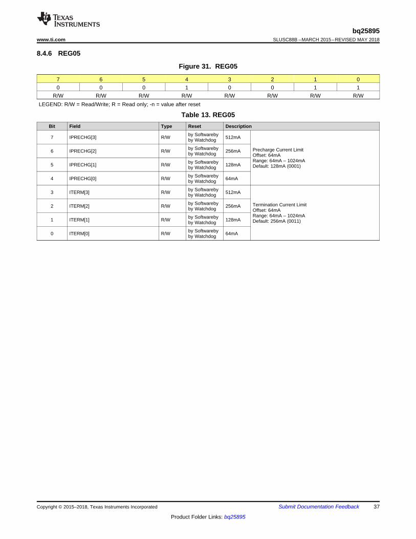
37
bq25895www.ti.com SLUSC88B –MARCH 2015–REVISED MAY 2018
Product Folder Links: bq25895
Submit Documentation FeedbackCopyright © 2015–2018, Texas Instruments Incorporated
8.4.6 REG05
Figure 31. REG05
7 6 5 4 3 2 1 00 0 0 1 0 0 1 1
R/W R/W R/W R/W R/W R/W R/W R/WLEGEND: R/W = Read/Write; R = Read only; -n = value after reset
Table 13. REG05Bit Field Type Reset Description
7 IPRECHG[3] R/W by Softwarebyby Watchdog 512mA
Precharge Current LimitOffset: 64mARange: 64mA – 1024mADefault: 128mA (0001)
6 IPRECHG[2] R/W by Softwarebyby Watchdog 256mA
5 IPRECHG[1] R/W by Softwarebyby Watchdog 128mA
4 IPRECHG[0] R/W by Softwarebyby Watchdog 64mA
3 ITERM[3] R/W by Softwarebyby Watchdog 512mA
Termination Current LimitOffset: 64mARange: 64mA – 1024mADefault: 256mA (0011)
2 ITERM[2] R/W by Softwarebyby Watchdog 256mA
1 ITERM[1] R/W by Softwarebyby Watchdog 128mA
0 ITERM[0] R/W by Softwarebyby Watchdog 64mA

38
bq25895SLUSC88B –MARCH 2015–REVISED MAY 2018 www.ti.com
Product Folder Links: bq25895
Submit Documentation Feedback Copyright © 2015–2018, Texas Instruments Incorporated
8.4.7 REG06
Figure 32. REG06
7 6 5 4 3 2 1 00 1 0 1 1 1 1 0
R/W R/W R/W R/W R/W R/W R/W R/WLEGEND: R/W = Read/Write; R = Read only; -n = value after reset
Table 14. REG06Bit Field Type Reset Description
7 VREG[5] R/W by Softwarebyby Watchdog 512mV
Charge Voltage LimitOffset: 3.840VRange: 3.840V – 4.608V (110000)Default: 4.208V (010111)Note:VREG > 110000 (4.608V) is clamped to register value110000 (4.608V)
6 VREG[4] R/W by Softwarebyby Watchdog 256mV
5 VREG[3] R/W by Softwarebyby Watchdog 128mV
4 VREG[2] R/W by Softwarebyby Watchdog 64mV
3 VREG[1] R/W by Softwarebyby Watchdog 32mV
2 VREG[0] R/W by Softwarebyby Watchdog 16mV
1 BATLOWV R/W by Softwarebyby Watchdog
Battery Precharge to Fast Charge Threshold0 – 2.8V1 – 3.0V (default)
0 VRECHG R/W by Softwarebyby Watchdog
Battery Recharge Threshold Offset(below Charge Voltage Limit)0 – 100mV (VRECHG) below VREG (REG06[7:2]) (default)1 – 200mV (VRECHG) below VREG (REG06[7:2])

39
bq25895www.ti.com SLUSC88B –MARCH 2015–REVISED MAY 2018
Product Folder Links: bq25895
Submit Documentation FeedbackCopyright © 2015–2018, Texas Instruments Incorporated
8.4.8 REG07
Figure 33. REG07
7 6 5 4 3 2 1 01 0 0 1 1 1 0 1
R/W R/W R/W R/W R/W R/W R/W R/WLEGEND: R/W = Read/Write; R = Read only; -n = value after reset
Table 15. REG07Bit Field Type Reset Description
7 EN_TERM R/W by Softwarebyby Watchdog
Charging Termination Enable0 – Disable1 – Enable (default)
6 STAT_DIS R/W by Softwarebyby Watchdog
STAT Pin Disable0 – Enable STAT pin function (default)1 – Disable STAT pin function
5 WATCHDOG[1] R/W by Softwarebyby Watchdog
I2C Watchdog Timer Setting00 – Disable watchdog timer01 – 40s (default)10 – 80s11 – 160s
4 WATCHDOG[0] R/W by Softwarebyby Watchdog
3 EN_TIMER R/W by Softwarebyby Watchdog
Charging Safety Timer Enable0 – Disable1 – Enable (default)
2 CHG_TIMER[1] R/W by Softwarebyby Watchdog
Fast Charge Timer Setting00 – 5 hrs01 – 8 hrs10 – 12 hrs (default)11 – 20 hrs
1 CHG_TIMER[0] R/W by Softwarebyby Watchdog
0 Reserved R/W Reserved (Default = 1)

40
bq25895SLUSC88B –MARCH 2015–REVISED MAY 2018 www.ti.com
Product Folder Links: bq25895
Submit Documentation Feedback Copyright © 2015–2018, Texas Instruments Incorporated
8.4.9 REG08
Figure 34. REG08
7 6 5 4 3 2 1 00 0 0 0 0 0 1 1
R/W R/W R/W R/W R/W R/W R/W R/WLEGEND: R/W = Read/Write; R = Read only; -n = value after reset
Table 16. REG08Bit Field Type Reset Description
7 BAT_COMP[2] R/W by Softwarebyby Watchdog 80mΩ
IR Compensation Resistor SettingRange: 0 – 140mΩDefault: 0Ω (000) (i.e. Disable IRComp)
6 BAT_COMP[1] R/W by Softwarebyby Watchdog 40mΩ
5 BAT_COMP[0] R/W by Softwarebyby Watchdog 20mΩ
4 VCLAMP[2] R/W by Softwarebyby Watchdog 128mV IR Compensation Voltage Clamp
above VREG (REG06[7:2])Offset: 0mVRange: 0-224mVDefault: 0mV (000)
3 VCLAMP[1] R/W by Softwarebyby Watchdog 64mV
2 VCLAMP[0] R/W by Softwarebyby Watchdog 32mV
1 TREG[1] R/W by Softwarebyby Watchdog
Thermal Regulation Threshold00 – 60°C01 – 80°C10 – 100°C11 – 120°C (default)
0 TREG[0] R/W by Softwarebyby Watchdog
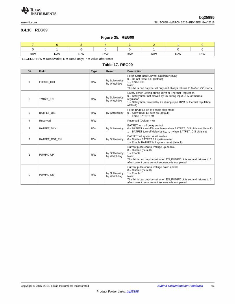
41
bq25895www.ti.com SLUSC88B –MARCH 2015–REVISED MAY 2018
Product Folder Links: bq25895
Submit Documentation FeedbackCopyright © 2015–2018, Texas Instruments Incorporated
8.4.10 REG09
Figure 35. REG09
7 6 5 4 3 2 1 00 1 0 0 0 1 0 0
R/W R/W R/W R/W R/W R/W R/W R/WLEGEND: R/W = Read/Write; R = Read only; -n = value after reset
Table 17. REG09Bit Field Type Reset Description
7 FORCE_ICO R/W by Softwarebyby Watchdog
Force Start Input Current Optimizer (ICO)0 – Do not force ICO (default)1 – Force ICONote:This bit is can only be set only and always returns to 0 after ICO starts
6 TMR2X_EN R/W by Softwarebyby Watchdog
Safety Timer Setting during DPM or Thermal Regulation0 – Safety timer not slowed by 2X during input DPM or thermalregulation1 – Safety timer slowed by 2X during input DPM or thermal regulation(default)
5 BATFET_DIS R/W by SoftwarebyForce BATFET off to enable ship mode0 – Allow BATFET turn on (default)1 – Force BATFET off
4 Reserved R/W Reserved (Default = 0)
3 BATFET_DLY R/W by SoftwarebyBATFET turn off delay control0 – BATFET turn off immediately when BATFET_DIS bit is set (default)1 – BATFET turn off delay by tSM_DLY when BATFET_DIS bit is set
2 BATFET_RST_EN R/W by SoftwarebyBATFET full system reset enable0 – Disable BATFET full system reset1 – Enable BATFET full system reset (default)
1 PUMPX_UP R/W by Softwarebyby Watchdog
Current pulse control voltage up enable0 – Disable (default)1 – EnableNote:This bit is can only be set when EN_PUMPX bit is set and returns to 0after current pulse control sequence is completed
0 PUMPX_DN R/W by Softwarebyby Watchdog
Current pulse control voltage down enable0 – Disable (default)1 – EnableNote:This bit is can only be set when EN_PUMPX bit is set and returns to 0after current pulse control sequence is completed

42
bq25895SLUSC88B –MARCH 2015–REVISED MAY 2018 www.ti.com
Product Folder Links: bq25895
Submit Documentation Feedback Copyright © 2015–2018, Texas Instruments Incorporated
8.4.11 REG0A
Figure 36. REG0A
7 6 5 4 3 2 1 01 0 0 1 0 0 1 1
R/W R/W R/W R/W R/W R/W R/W R/WLEGEND: R/W = Read/Write; R = Read only; -n = value after reset
Table 18. REG0ABit Field Type Reset Description
7 BOOSTV[3] R/W by Softwarebyby Watchdog 512mV
Boost Mode Voltage RegulationOffset: 4.55VRange: 4.55V – 5.51VDefault: 5.126V (1001)
6 BOOSTV[2] R/W by Softwarebyby Watchdog 256mV
5 BOOSTV[1] R/W by Softwareby 128mV
4 BOOSTV[0] R/W by Softwarebyby Watchdog 64mV
3 Reserved R/W by Softwareby Watchdog Reserved (default = 0)
2 Reserved R/W by Softwareby Watchdog Reserved (default = 0)
1 Reserved R/W by Softwareby Watchdog Reserved (default = 1)
0 Reserved R/W by Softwareby Watchdog Reserved (default = 1)
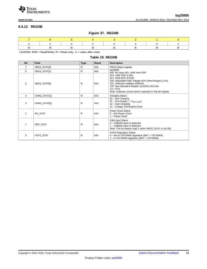
43
bq25895www.ti.com SLUSC88B –MARCH 2015–REVISED MAY 2018
Product Folder Links: bq25895
Submit Documentation FeedbackCopyright © 2015–2018, Texas Instruments Incorporated
8.4.12 REG0B
Figure 37. REG0B
7 6 5 4 3 2 1 0x x x x x x x xR R R R R R R R
LEGEND: R/W = Read/Write; R = Read only; -n = value after reset
Table 19. REG0BBit Field Type Reset Description
7 VBUS_STAT[2] R N/A VBUS Status registerbq25895000: No Input 001: USB Host SDP010: USB CDP (1.5A)011: USB DCP (3.25A)100: Adjustable High Voltage DCP (MaxCharge) (1.5A)101: Unknown Adapter (500mA)110: Non-Standard Adapter (1A/2A/2.1A/2.4A)111: OTGNote: Software current limit is reported in IINLIM register
6 VBUS_STAT[1] R N/A
5 VBUS_STAT[0] R N/A
4 CHRG_STAT[1] R N/A Charging Status00 – Not Charging01 – Pre-charge ( < VBATLOWV)10 – Fast Charging11 – Charge Termination Done
3 CHRG_STAT[0] R N/A
2 PG_STAT R N/APower Good Status0 – Not Power Good1 – Power Good
1 SDP_STAT R N/A
USB Input Status0 – USB100 input is detected1 – USB500 input is detectedNote: This bit always read 1 when VBUS_STAT is not 001
0 VSYS_STAT R N/AVSYS Regulation Status0 – Not in VSYSMIN regulation (BAT > VSYSMIN)1 – In VSYSMIN regulation (BAT < VSYSMIN)

44
bq25895SLUSC88B –MARCH 2015–REVISED MAY 2018 www.ti.com
Product Folder Links: bq25895
Submit Documentation Feedback Copyright © 2015–2018, Texas Instruments Incorporated
8.4.13 REG0C
Figure 38. REG0C
7 6 5 4 3 2 1 0x x x x x x x xR R R R R R R R
LEGEND: R/W = Read/Write; R = Read only; -n = value after reset
Table 20. REG0CBit Field Type Reset Description
7 WATCHDOG_FAULT R N/AWatchdog Fault StatusStatus 0 – Normal1- Watchdog timer expiration
6 BOOST_FAULT R N/A
Boost Mode Fault Status0 – Normal1 – VBUS overloaded in OTG, or VBUS OVP, or battery is too low inboost mode
5 CHRG_FAULT[1] R N/A Charge Fault Status00 – Normal01 – Input fault (VBUS > VACOV or VBAT < VBUS < VVBUSMIN(typical 3.8V))10 - Thermal shutdown11 – Charge Safety Timer Expiration
4 CHRG_FAULT[0] R N/A
3 BAT_FAULT R N/ABattery Fault Status0 – Normal1 – BATOVP (VBAT > VBATOVP)
2 NTC_FAULT[2] R N/A NTC Fault StatusBuck Mode:000 – Normal001 – TS Cold010 – TS HotBoost Mode:000 – Normal101 – TS Cold110 – TS Hot
1 NTC_FAULT[1] R N/A
0 NTC_FAULT[0] R N/A

45
bq25895www.ti.com SLUSC88B –MARCH 2015–REVISED MAY 2018
Product Folder Links: bq25895
Submit Documentation FeedbackCopyright © 2015–2018, Texas Instruments Incorporated
8.4.14 REG0D
Figure 39. REG0D
7 6 5 4 3 2 1 00 0 0 1 0 0 1 0
R/W R/W R/W R/W R/W R/W R/W R/WLEGEND: R/W = Read/Write; R = Read only; -n = value after reset
Table 21. REG0DBit Field Type Reset Description
7 FORCE_VINDPM R/W by SoftwarebyVINDPM Threshold Setting Method0 – Run Relative VINDPM Threshold (default)1 – Run Absolute VINDPM Threshold
6 VINDPM[6] R/W by Softwareby 6400mV Absolute VINDPM ThresholdOffset: 2.6VRange: 3.9V (0001101) – 15.3V (1111111)Default: 4.4V (0010010)Note:Value < 0001101 is clamped to 3.9V (0001101)Register is read only when FORCE_VINDPM=0 and canbe written by internal control based on relative VINDPMthreshold settingRegister can be read/write when FORCE_VINDPM = 1
5 VINDPM[5] R/W by Softwareby 3200mV
4 VINDPM[4] R/W by Softwareby 1600mV
3 VINDPM[3] R/W by Softwareby 800mV
2 VINDPM[2] R/W by Softwareby 400mV
1 VINDPM[1] R/W by Softwareby 200mV
0 VINDPM[0] R/W by Softwareby 100mV
8.4.15 REG0E
Figure 40. REG0E
7 6 5 4 3 2 1 00 0 0 0 0 0 0 0R R R R R R R R
LEGEND: R/W = Read/Write; R = Read only; -n = value after reset
Table 22. REG0EBit Field Type Reset Description
7 THERM_STAT R N/AThermal Regulation Status0 – Normal1 – In Thermal Regulation
6 BATV[6] R N/A 1280mV
ADC conversion of Battery Voltage (VBAT)Offset: 2.304VRange: 2.304V (0000000) – 4.848V (1111111)Default: 2.304V (0000000)
5 BATV[5] R N/A 640mV
4 BATV[4] R N/A 320mV
3 BATV[3] R N/A 160mV
2 BATV[2] R N/A 80mV
1 BATV[1] R N/A 40mV
0 BATV[0] R N/A 20mV
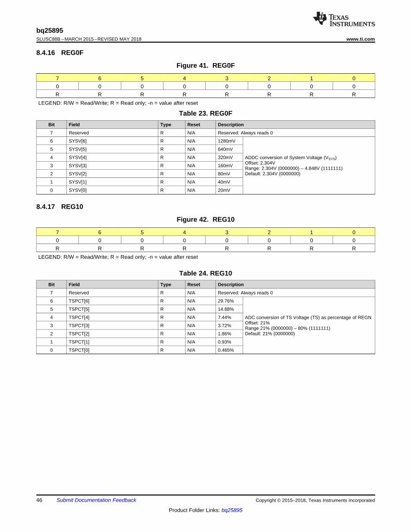
46
bq25895SLUSC88B –MARCH 2015–REVISED MAY 2018 www.ti.com
Product Folder Links: bq25895
Submit Documentation Feedback Copyright © 2015–2018, Texas Instruments Incorporated
8.4.16 REG0F
Figure 41. REG0F
7 6 5 4 3 2 1 00 0 0 0 0 0 0 0R R R R R R R R
LEGEND: R/W = Read/Write; R = Read only; -n = value after reset
Table 23. REG0FBit Field Type Reset Description
7 Reserved R N/A Reserved: Always reads 0
6 SYSV[6] R N/A 1280mV
ADDC conversion of System Voltage (VSYS)Offset: 2.304VRange: 2.304V (0000000) – 4.848V (1111111)Default: 2.304V (0000000)
5 SYSV[5] R N/A 640mV
4 SYSV[4] R N/A 320mV
3 SYSV[3] R N/A 160mV
2 SYSV[2] R N/A 80mV
1 SYSV[1] R N/A 40mV
0 SYSV[0] R N/A 20mV
8.4.17 REG10
Figure 42. REG10
7 6 5 4 3 2 1 00 0 0 0 0 0 0 0R R R R R R R R
LEGEND: R/W = Read/Write; R = Read only; -n = value after reset
Table 24. REG10Bit Field Type Reset Description
7 Reserved R N/A Reserved: Always reads 0
6 TSPCT[6] R N/A 29.76%
ADC conversion of TS Voltage (TS) as percentage of REGNOffset: 21%Range 21% (0000000) – 80% (1111111)Default: 21% (0000000)
5 TSPCT[5] R N/A 14.88%
4 TSPCT[4] R N/A 7.44%
3 TSPCT[3] R N/A 3.72%
2 TSPCT[2] R N/A 1.86%
1 TSPCT[1] R N/A 0.93%
0 TSPCT[0] R N/A 0.465%
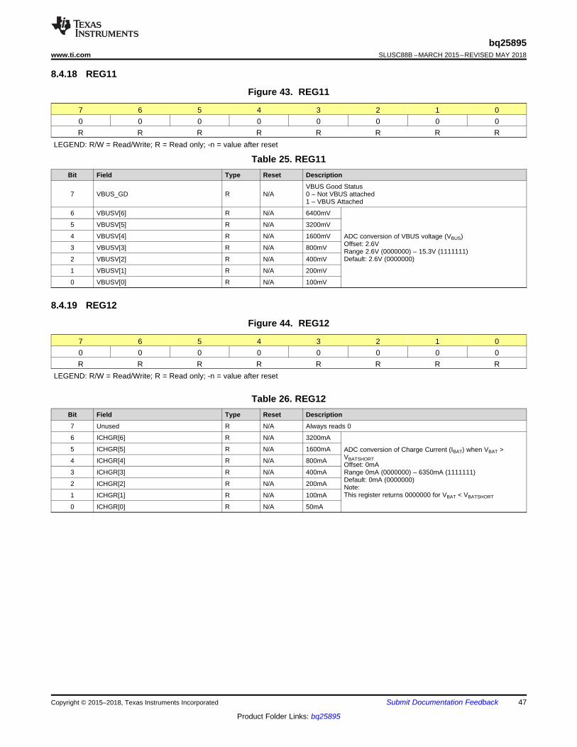
47
bq25895www.ti.com SLUSC88B –MARCH 2015–REVISED MAY 2018
Product Folder Links: bq25895
Submit Documentation FeedbackCopyright © 2015–2018, Texas Instruments Incorporated
8.4.18 REG11
Figure 43. REG11
7 6 5 4 3 2 1 00 0 0 0 0 0 0 0R R R R R R R R
LEGEND: R/W = Read/Write; R = Read only; -n = value after reset
Table 25. REG11Bit Field Type Reset Description
7 VBUS_GD R N/AVBUS Good Status0 – Not VBUS attached1 – VBUS Attached
6 VBUSV[6] R N/A 6400mV
ADC conversion of VBUS voltage (VBUS)Offset: 2.6VRange 2.6V (0000000) – 15.3V (1111111)Default: 2.6V (0000000)
5 VBUSV[5] R N/A 3200mV
4 VBUSV[4] R N/A 1600mV
3 VBUSV[3] R N/A 800mV
2 VBUSV[2] R N/A 400mV
1 VBUSV[1] R N/A 200mV
0 VBUSV[0] R N/A 100mV
8.4.19 REG12
Figure 44. REG12
7 6 5 4 3 2 1 00 0 0 0 0 0 0 0R R R R R R R R
LEGEND: R/W = Read/Write; R = Read only; -n = value after reset
Table 26. REG12Bit Field Type Reset Description
7 Unused R N/A Always reads 0
6 ICHGR[6] R N/A 3200mA
ADC conversion of Charge Current (IBAT) when VBAT >VBATSHORTOffset: 0mARange 0mA (0000000) – 6350mA (1111111)Default: 0mA (0000000)Note:This register returns 0000000 for VBAT < VBATSHORT
5 ICHGR[5] R N/A 1600mA
4 ICHGR[4] R N/A 800mA
3 ICHGR[3] R N/A 400mA
2 ICHGR[2] R N/A 200mA
1 ICHGR[1] R N/A 100mA
0 ICHGR[0] R N/A 50mA

48
bq25895SLUSC88B –MARCH 2015–REVISED MAY 2018 www.ti.com
Product Folder Links: bq25895
Submit Documentation Feedback Copyright © 2015–2018, Texas Instruments Incorporated
8.4.20 REG13
Figure 45. REG13
7 6 5 4 3 2 1 00 0 0 0 0 0 0 0R R R R R R R R
LEGEND: R/W = Read/Write; R = Read only; -n = value after reset
Table 27. REG13Bit Field Type Reset Description
7 VDPM_STAT R N/AVINDPM Status0 – Not in VINDPM1 – VINDPM
6 IDPM_STAT R N/AIINDPM Status0 – Not in IINDPM1 – IINDPM
5 IDPM_LIM[5] R N/A 1600mA
Input Current Limit in effect while Input Current Optimizer(ICO) is enabledOffset: 100mA (default)Range 100mA (0000000) – 3.25mA (1111111)
4 IDPM_LIM[4] R N/A 800mA
3 IDPM_LIM[3] R N/A 400mA
2 IDPM_LIM[2] R N/A 200mA
1 IDPM_LIM[1] R N/A 100mA
0 IDPM_LIM[0] R N/A 50mA
8.4.21 REG14
Figure 46. REG14
7 6 5 4 3 2 1 00 0 0 0 0 0 0 0
R/W R/W R R R R R RLEGEND: R/W = Read/Write; R = Read only; -n = value after reset
Table 28. REG14Bit Field Type Reset Description
7 REG_RST R/W N/A
Register Reset0 – Keep current register setting (default)1 – Reset to default register value and reset safety timerNote:Reset to 0 after register reset is completed
6 ICO_OPTIMIZED R N/AInput Current Optimizer (ICO) Status0 – Optimization is in progress1 – Maximum Input Current Detected
5 PN[2] R N/ADevice Configuration111: bq258954 PN[1] R N/A
3 PN[0] R N/A
2 TS_PROFILE R N/A Temperature Profile0 – Cold/Hot (default)
1 DEV_REV[1] R N/ADevice Revision: 01
0 DEV_REV[0] R N/A
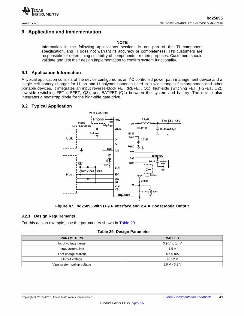
VBUS
D+
D-
SDA
SCL
INT
OTG
/CE
SW
BTST
REGN
PGND
SYS
BAT
TS
VREF
REGN
bq25895
Host
Input3.9V±14V at 3A
USB
Ichg=5A
QON
2.2H
ILIM
1F
10uF
10F
SYS 3.5V±4.5V
10F47nF
4.7F
Optional
260Q
10<Q10<Q10<Q
5.23<Q
30.1<Q 10<Q
PMIDPhone
5V at 2.4A OTG
40F
STAT
SYS
2.2<Q
49
bq25895www.ti.com SLUSC88B –MARCH 2015–REVISED MAY 2018
Product Folder Links: bq25895
Submit Documentation FeedbackCopyright © 2015–2018, Texas Instruments Incorporated
9 Application and Implementation
NOTEInformation in the following applications sections is not part of the TI componentspecification, and TI does not warrant its accuracy or completeness. TI’s customers areresponsible for determining suitability of components for their purposes. Customers shouldvalidate and test their design implementation to confirm system functionality.
9.1 Application InformationA typical application consists of the device configured as an I2C controlled power path management device and asingle cell battery charger for Li-Ion and Li-polymer batteries used in a wide range of smartphones and otherportable devices. It integrates an input reverse-block FET (RBFET, Q1), high-side switching FET (HSFET, Q2),low-side switching FET (LSFET, Q3), and BATFET (Q4) between the system and battery. The device alsointegrates a bootstrap diode for the high-side gate drive.
9.2 Typical Application
Figure 47. bq25895 with D+/D- Interface and 2.4 A Boost Mode Output
9.2.1 Design RequirementsFor this design example, use the parameters shown in Table 29.
Table 29. Design ParameterPARAMETERS VALUES
Input voltage range 3.9 V to 14 VInput current limit 1.5 A
Fast charge current 5000 mAOutput voltage 4.352 V
VREF system pullup voltage 1.8 V - 3.3 V

PMID CHGI = I x D x (1 - D)
BUSRIPPLE
V x D x (1-D)I =
s x Lf
BAT CHG RIPPLEI I + (1/2) I³
50
bq25895SLUSC88B –MARCH 2015–REVISED MAY 2018 www.ti.com
Product Folder Links: bq25895
Submit Documentation Feedback Copyright © 2015–2018, Texas Instruments Incorporated
9.2.2 Detailed Design Procedure
9.2.2.1 Custom Design With WEBENCH® ToolsClick here to create a custom design using the bq25895 device with the WEBENCH® Power Designer.1. Start by entering the input voltage (VIN), output voltage (VOUT), and output current (IOUT) requirements.2. Optimize the design for key parameters such as efficiency, footprint, and cost using the optimizer dial.3. Compare the generated design with other possible solutions from Texas Instruments.
The WEBENCH Power Designer provides a customized schematic along with a list of materials with real-timepricing and component availability.
In most cases, these actions are available:• Run electrical simulations to see important waveforms and circuit performance• Run thermal simulations to understand board thermal performance• Export customized schematic and layout into popular CAD formats• Print PDF reports for the design, and share the design with colleagues
Get more information about WEBENCH tools at www.ti.com/WEBENCH.
9.2.2.2 Inductor SelectionThe device has 1.5 MHz switching frequency to allow the use of small inductor and capacitor values. TheInductor saturation current should be higher than the charging current (ICHG) plus half the ripple current (IRIPPLE):
(5)
The inductor ripple current depends on input voltage (VBUS), duty cycle (D = VBAT/VVBUS), switching frequency (fs)and inductance (L):
(6)
The maximum inductor ripple current happens with D = 0.5 or close to 0.5. Usually inductor ripple is designed inthe range of (20–40%) maximum charging current as a trade-off between inductor size and efficiency for apractical design.
9.2.2.3 Buck Input Capacitor
Input capacitor should have enough ripple current rating to absorb input switching ripple current. The worst caseRMS ripple current is half of the charging current when duty cycle is 0.5. If the converter does not operate at50% duty cycle, then the worst case capacitor RMS current IPMID occurs where the duty cycle is closest to 50%and can be estimated by Equation 7:
(7)
Low ESR ceramic capacitor such as X7R or X5R is preferred for input decoupling capacitor and should beplaced to the drain of the high side MOSFET and source of the low side MOSFET as close as possible. Voltagerating of the capacitor must be higher than normal input voltage level. 25 V rating or higher capacitor is preferredfor up to 14-V input voltage. 8.2-μF capacitance is suggested for typical of 3 A – 5 A charging current.
SYS SYSO 2
BUSSYS
V VV = 1
V8 LC sf
æ ö÷ç ÷D ç - ÷ç ÷÷çè ø
RIPPLECSYS RIPPLE
II = 0.29 x I
2 x 3»
51
bq25895www.ti.com SLUSC88B –MARCH 2015–REVISED MAY 2018
Product Folder Links: bq25895
Submit Documentation FeedbackCopyright © 2015–2018, Texas Instruments Incorporated
9.2.2.4 System Output Capacitor
Output capacitor also should have enough ripple current rating to absorb output switching ripple current. Theoutput capacitor RMS current ICOUT is given:
(8)
The output capacitor voltage ripple can be calculated as follows:
(9)
At certain input/output voltage and switching frequency, the voltage ripple can be reduced by increasing theoutput filter LC. The charger device has internal loop compensator. To get good loop stability, 1-µH and minimumof 20-µF output capacitor is recommended. The preferred ceramic capacitor is 6V or higher rating, X7R or X5R.
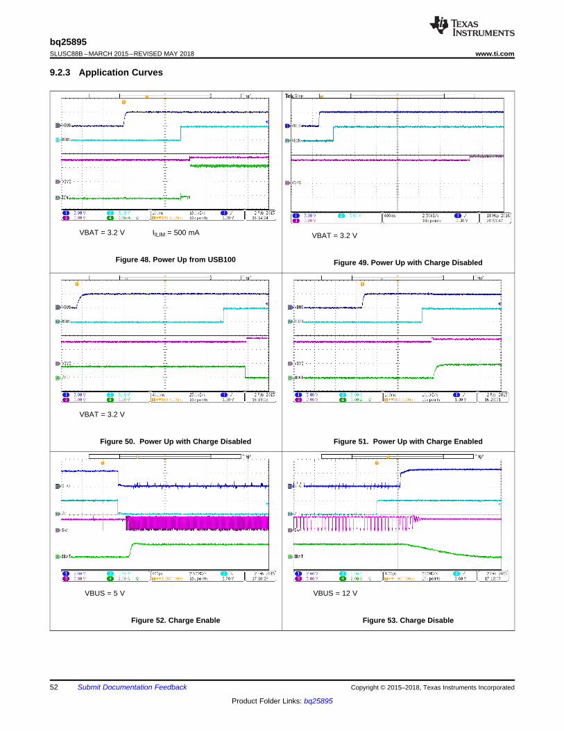
52
bq25895SLUSC88B –MARCH 2015–REVISED MAY 2018 www.ti.com
Product Folder Links: bq25895
Submit Documentation Feedback Copyright © 2015–2018, Texas Instruments Incorporated
9.2.3 Application Curves
VBAT = 3.2 V IILIM = 500 mA
Figure 48. Power Up from USB100
VBAT = 3.2 V
Figure 49. Power Up with Charge Disabled
VBAT = 3.2 V
Figure 50. Power Up with Charge Disabled Figure 51. Power Up with Charge Enabled
VBUS = 5 V
Figure 52. Charge Enable
VBUS = 12 V
Figure 53. Charge Disable

53
bq25895www.ti.com SLUSC88B –MARCH 2015–REVISED MAY 2018
Product Folder Links: bq25895
Submit Documentation FeedbackCopyright © 2015–2018, Texas Instruments Incorporated
VBUS = 5 V IIN = 3 A Charge Disable
Figure 54. Input Current DPM Response without Battery
VBUS = 9 V IIN = 1.5 A VBAT = 3.8 VICHG = 2 A ISYS = 0 A - 4 A
Figure 55. Load Transient During Supplement Mode
VBUS = 12 V VBAT = 3.8 V ICHG = 3 A
Figure 56. PWM Switching Waveform
VBUS = 9V ISYS = 10 mA, Charge DisableNo Battery
Figure 57. PFM Switching Waveform
VBAT = 3.8 V ILOAD = 1 A
Figure 58. Boost Mode Switching Waveform
VBAT = 3.8 V ILOAD = 0 A - 1 A
Figure 59. Boost Mode Load Transient

VBUS
D+
D-
SDA
SCL
INT
OTG
/CE
SW
BTST
REGN
PGND
SYS
BAT
TS
VREF
REGN
bq25895
Host
Input3.9V±14V at 3A
USB
Ichg=5A
QON
2.2H
ILIM
1F
10uF
10F
SYS 3.5V±4.5V
10F47nF
4.7F
Optional
260Q
10<Q10<Q10<Q
10<Q
10<Q
PMIDPhone
5V at 3.1A OTG
60F
NSR10F20NXT5G
STAT
SYS
2.2<Q
54
bq25895SLUSC88B –MARCH 2015–REVISED MAY 2018 www.ti.com
Product Folder Links: bq25895
Submit Documentation Feedback Copyright © 2015–2018, Texas Instruments Incorporated
9.3 System Examples
Figure 60. bq25895 with D+/D- Interface, 3.1 A Boost Mode Output, and no Thermistor Connections
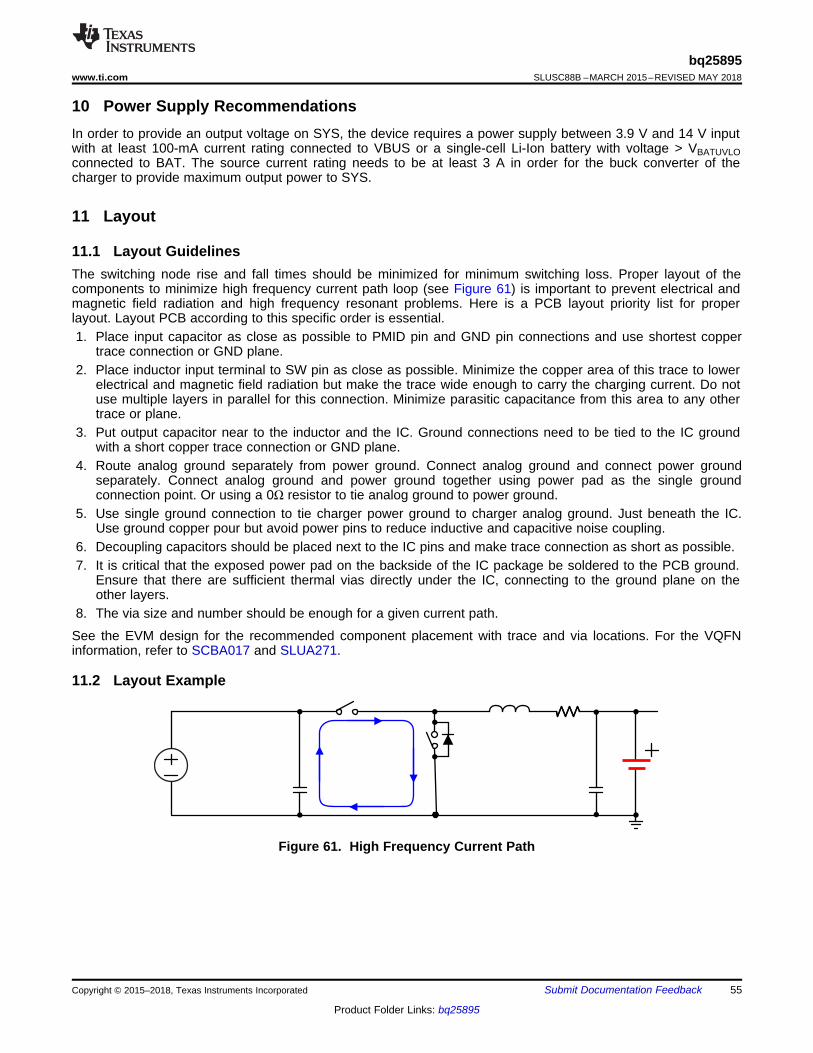
55
bq25895www.ti.com SLUSC88B –MARCH 2015–REVISED MAY 2018
Product Folder Links: bq25895
Submit Documentation FeedbackCopyright © 2015–2018, Texas Instruments Incorporated
10 Power Supply RecommendationsIn order to provide an output voltage on SYS, the device requires a power supply between 3.9 V and 14 V inputwith at least 100-mA current rating connected to VBUS or a single-cell Li-Ion battery with voltage > VBATUVLOconnected to BAT. The source current rating needs to be at least 3 A in order for the buck converter of thecharger to provide maximum output power to SYS.
11 Layout
11.1 Layout GuidelinesThe switching node rise and fall times should be minimized for minimum switching loss. Proper layout of thecomponents to minimize high frequency current path loop (see Figure 61) is important to prevent electrical andmagnetic field radiation and high frequency resonant problems. Here is a PCB layout priority list for properlayout. Layout PCB according to this specific order is essential.1. Place input capacitor as close as possible to PMID pin and GND pin connections and use shortest copper
trace connection or GND plane.2. Place inductor input terminal to SW pin as close as possible. Minimize the copper area of this trace to lower
electrical and magnetic field radiation but make the trace wide enough to carry the charging current. Do notuse multiple layers in parallel for this connection. Minimize parasitic capacitance from this area to any othertrace or plane.
3. Put output capacitor near to the inductor and the IC. Ground connections need to be tied to the IC groundwith a short copper trace connection or GND plane.
4. Route analog ground separately from power ground. Connect analog ground and connect power groundseparately. Connect analog ground and power ground together using power pad as the single groundconnection point. Or using a 0Ω resistor to tie analog ground to power ground.
5. Use single ground connection to tie charger power ground to charger analog ground. Just beneath the IC.Use ground copper pour but avoid power pins to reduce inductive and capacitive noise coupling.
6. Decoupling capacitors should be placed next to the IC pins and make trace connection as short as possible.7. It is critical that the exposed power pad on the backside of the IC package be soldered to the PCB ground.
Ensure that there are sufficient thermal vias directly under the IC, connecting to the ground plane on theother layers.
8. The via size and number should be enough for a given current path.
See the EVM design for the recommended component placement with trace and via locations. For the VQFNinformation, refer to SCBA017 and SLUA271.
11.2 Layout Example
Figure 61. High Frequency Current Path

56
bq25895SLUSC88B –MARCH 2015–REVISED MAY 2018 www.ti.com
Product Folder Links: bq25895
Submit Documentation Feedback Copyright © 2015–2018, Texas Instruments Incorporated
12 Device and Documentation Support
12.1 Development Support
12.1.1 Custom Design With WEBENCH® ToolsClick here to create a custom design using the bq25895 device with the WEBENCH® Power Designer.1. Start by entering the input voltage (VIN), output voltage (VOUT), and output current (IOUT) requirements.2. Optimize the design for key parameters such as efficiency, footprint, and cost using the optimizer dial.3. Compare the generated design with other possible solutions from Texas Instruments.
The WEBENCH Power Designer provides a customized schematic along with a list of materials with real-timepricing and component availability.
In most cases, these actions are available:• Run electrical simulations to see important waveforms and circuit performance• Run thermal simulations to understand board thermal performance• Export customized schematic and layout into popular CAD formats• Print PDF reports for the design, and share the design with colleagues
Get more information about WEBENCH tools at www.ti.com/WEBENCH.
12.2 Receiving Notification of Documentation UpdatesTo receive notification of documentation updates, navigate to the device product folder on ti.com. In the upperright corner, click on Alert me to register and receive a weekly digest of any product information that haschanged. For change details, review the revision history included in any revised document.
12.3 Community ResourcesThe following links connect to TI community resources. Linked contents are provided "AS IS" by the respectivecontributors. They do not constitute TI specifications and do not necessarily reflect TI's views; see TI's Terms ofUse.
TI E2E™ Online Community TI's Engineer-to-Engineer (E2E) Community. Created to foster collaborationamong engineers. At e2e.ti.com, you can ask questions, share knowledge, explore ideas and helpsolve problems with fellow engineers.
Design Support TI's Design Support Quickly find helpful E2E forums along with design support tools andcontact information for technical support.
12.4 TrademarksPowerPAD, E2E are trademarks of Texas Instruments.WEBENCH is a registered trademark of Texas Instruments.All other trademarks are the property of their respective owners.
12.5 Electrostatic Discharge CautionThese devices have limited built-in ESD protection. The leads should be shorted together or the device placed in conductive foamduring storage or handling to prevent electrostatic damage to the MOS gates.
12.6 GlossarySLYZ022 — TI Glossary.
This glossary lists and explains terms, acronyms, and definitions.
13 Mechanical, Packaging, and Orderable InformationThe following pages include mechanical, packaging, and orderable information. This information is the mostcurrent data available for the designated devices. This data is subject to change without notice and revision ofthis document. For browser-based versions of this data sheet, refer to the left-hand navigation.

PACKAGE OPTION ADDENDUM
www.ti.com 4-May-2018
Addendum-Page 1
PACKAGING INFORMATION
Orderable Device Status(1)
Package Type PackageDrawing
Pins PackageQty
Eco Plan(2)
Lead/Ball Finish(6)
MSL Peak Temp(3)
Op Temp (°C) Device Marking(4/5)
Samples
BQ25895RTWR ACTIVE WQFN RTW 24 3000 Green (RoHS& no Sb/Br)
CU NIPDAU Level-2-260C-1 YEAR -40 to 85 BQ25895
BQ25895RTWT ACTIVE WQFN RTW 24 250 Green (RoHS& no Sb/Br)
CU NIPDAU Level-2-260C-1 YEAR -40 to 85 BQ25895
(1) The marketing status values are defined as follows:ACTIVE: Product device recommended for new designs.LIFEBUY: TI has announced that the device will be discontinued, and a lifetime-buy period is in effect.NRND: Not recommended for new designs. Device is in production to support existing customers, but TI does not recommend using this part in a new design.PREVIEW: Device has been announced but is not in production. Samples may or may not be available.OBSOLETE: TI has discontinued the production of the device.
(2) RoHS: TI defines "RoHS" to mean semiconductor products that are compliant with the current EU RoHS requirements for all 10 RoHS substances, including the requirement that RoHS substancedo not exceed 0.1% by weight in homogeneous materials. Where designed to be soldered at high temperatures, "RoHS" products are suitable for use in specified lead-free processes. TI mayreference these types of products as "Pb-Free".RoHS Exempt: TI defines "RoHS Exempt" to mean products that contain lead but are compliant with EU RoHS pursuant to a specific EU RoHS exemption.Green: TI defines "Green" to mean the content of Chlorine (Cl) and Bromine (Br) based flame retardants meet JS709B low halogen requirements of <=1000ppm threshold. Antimony trioxide basedflame retardants must also meet the <=1000ppm threshold requirement.
(3) MSL, Peak Temp. - The Moisture Sensitivity Level rating according to the JEDEC industry standard classifications, and peak solder temperature.
(4) There may be additional marking, which relates to the logo, the lot trace code information, or the environmental category on the device.
(5) Multiple Device Markings will be inside parentheses. Only one Device Marking contained in parentheses and separated by a "~" will appear on a device. If a line is indented then it is a continuationof the previous line and the two combined represent the entire Device Marking for that device.
(6) Lead/Ball Finish - Orderable Devices may have multiple material finish options. Finish options are separated by a vertical ruled line. Lead/Ball Finish values may wrap to two lines if the finishvalue exceeds the maximum column width.
Important Information and Disclaimer:The information provided on this page represents TI's knowledge and belief as of the date that it is provided. TI bases its knowledge and belief on informationprovided by third parties, and makes no representation or warranty as to the accuracy of such information. Efforts are underway to better integrate information from third parties. TI has taken andcontinues to take reasonable steps to provide representative and accurate information but may not have conducted destructive testing or chemical analysis on incoming materials and chemicals.TI and TI suppliers consider certain information to be proprietary, and thus CAS numbers and other limited information may not be available for release.
In no event shall TI's liability arising out of such information exceed the total purchase price of the TI part(s) at issue in this document sold by TI to Customer on an annual basis.

PACKAGE OPTION ADDENDUM
www.ti.com 4-May-2018
Addendum-Page 2

TAPE AND REEL INFORMATION
*All dimensions are nominal
Device PackageType
PackageDrawing
Pins SPQ ReelDiameter
(mm)
ReelWidth
W1 (mm)
A0(mm)
B0(mm)
K0(mm)
P1(mm)
W(mm)
Pin1Quadrant
BQ25895RTWR WQFN RTW 24 3000 330.0 12.4 4.25 4.25 1.15 8.0 12.0 Q2
BQ25895RTWT WQFN RTW 24 250 180.0 12.4 4.25 4.25 1.15 8.0 12.0 Q2
PACKAGE MATERIALS INFORMATION
www.ti.com 4-May-2018
Pack Materials-Page 1

*All dimensions are nominal
Device Package Type Package Drawing Pins SPQ Length (mm) Width (mm) Height (mm)
BQ25895RTWR WQFN RTW 24 3000 367.0 367.0 35.0
BQ25895RTWT WQFN RTW 24 250 210.0 185.0 35.0
PACKAGE MATERIALS INFORMATION
www.ti.com 4-May-2018
Pack Materials-Page 2


IMPORTANT NOTICE
Texas Instruments Incorporated (TI) reserves the right to make corrections, enhancements, improvements and other changes to itssemiconductor products and services per JESD46, latest issue, and to discontinue any product or service per JESD48, latest issue. Buyersshould obtain the latest relevant information before placing orders and should verify that such information is current and complete.TI’s published terms of sale for semiconductor products (http://www.ti.com/sc/docs/stdterms.htm) apply to the sale of packaged integratedcircuit products that TI has qualified and released to market. Additional terms may apply to the use or sale of other types of TI products andservices.Reproduction of significant portions of TI information in TI data sheets is permissible only if reproduction is without alteration and isaccompanied by all associated warranties, conditions, limitations, and notices. TI is not responsible or liable for such reproduceddocumentation. Information of third parties may be subject to additional restrictions. Resale of TI products or services with statementsdifferent from or beyond the parameters stated by TI for that product or service voids all express and any implied warranties for theassociated TI product or service and is an unfair and deceptive business practice. TI is not responsible or liable for any such statements.Buyers and others who are developing systems that incorporate TI products (collectively, “Designers”) understand and agree that Designersremain responsible for using their independent analysis, evaluation and judgment in designing their applications and that Designers havefull and exclusive responsibility to assure the safety of Designers' applications and compliance of their applications (and of all TI productsused in or for Designers’ applications) with all applicable regulations, laws and other applicable requirements. Designer represents that, withrespect to their applications, Designer has all the necessary expertise to create and implement safeguards that (1) anticipate dangerousconsequences of failures, (2) monitor failures and their consequences, and (3) lessen the likelihood of failures that might cause harm andtake appropriate actions. Designer agrees that prior to using or distributing any applications that include TI products, Designer willthoroughly test such applications and the functionality of such TI products as used in such applications.TI’s provision of technical, application or other design advice, quality characterization, reliability data or other services or information,including, but not limited to, reference designs and materials relating to evaluation modules, (collectively, “TI Resources”) are intended toassist designers who are developing applications that incorporate TI products; by downloading, accessing or using TI Resources in anyway, Designer (individually or, if Designer is acting on behalf of a company, Designer’s company) agrees to use any particular TI Resourcesolely for this purpose and subject to the terms of this Notice.TI’s provision of TI Resources does not expand or otherwise alter TI’s applicable published warranties or warranty disclaimers for TIproducts, and no additional obligations or liabilities arise from TI providing such TI Resources. TI reserves the right to make corrections,enhancements, improvements and other changes to its TI Resources. TI has not conducted any testing other than that specificallydescribed in the published documentation for a particular TI Resource.Designer is authorized to use, copy and modify any individual TI Resource only in connection with the development of applications thatinclude the TI product(s) identified in such TI Resource. NO OTHER LICENSE, EXPRESS OR IMPLIED, BY ESTOPPEL OR OTHERWISETO ANY OTHER TI INTELLECTUAL PROPERTY RIGHT, AND NO LICENSE TO ANY TECHNOLOGY OR INTELLECTUAL PROPERTYRIGHT OF TI OR ANY THIRD PARTY IS GRANTED HEREIN, including but not limited to any patent right, copyright, mask work right, orother intellectual property right relating to any combination, machine, or process in which TI products or services are used. Informationregarding or referencing third-party products or services does not constitute a license to use such products or services, or a warranty orendorsement thereof. Use of TI Resources may require a license from a third party under the patents or other intellectual property of thethird party, or a license from TI under the patents or other intellectual property of TI.TI RESOURCES ARE PROVIDED “AS IS” AND WITH ALL FAULTS. TI DISCLAIMS ALL OTHER WARRANTIES ORREPRESENTATIONS, EXPRESS OR IMPLIED, REGARDING RESOURCES OR USE THEREOF, INCLUDING BUT NOT LIMITED TOACCURACY OR COMPLETENESS, TITLE, ANY EPIDEMIC FAILURE WARRANTY AND ANY IMPLIED WARRANTIES OFMERCHANTABILITY, FITNESS FOR A PARTICULAR PURPOSE, AND NON-INFRINGEMENT OF ANY THIRD PARTY INTELLECTUALPROPERTY RIGHTS. TI SHALL NOT BE LIABLE FOR AND SHALL NOT DEFEND OR INDEMNIFY DESIGNER AGAINST ANY CLAIM,INCLUDING BUT NOT LIMITED TO ANY INFRINGEMENT CLAIM THAT RELATES TO OR IS BASED ON ANY COMBINATION OFPRODUCTS EVEN IF DESCRIBED IN TI RESOURCES OR OTHERWISE. IN NO EVENT SHALL TI BE LIABLE FOR ANY ACTUAL,DIRECT, SPECIAL, COLLATERAL, INDIRECT, PUNITIVE, INCIDENTAL, CONSEQUENTIAL OR EXEMPLARY DAMAGES INCONNECTION WITH OR ARISING OUT OF TI RESOURCES OR USE THEREOF, AND REGARDLESS OF WHETHER TI HAS BEENADVISED OF THE POSSIBILITY OF SUCH DAMAGES.Unless TI has explicitly designated an individual product as meeting the requirements of a particular industry standard (e.g., ISO/TS 16949and ISO 26262), TI is not responsible for any failure to meet such industry standard requirements.Where TI specifically promotes products as facilitating functional safety or as compliant with industry functional safety standards, suchproducts are intended to help enable customers to design and create their own applications that meet applicable functional safety standardsand requirements. Using products in an application does not by itself establish any safety features in the application. Designers mustensure compliance with safety-related requirements and standards applicable to their applications. Designer may not use any TI products inlife-critical medical equipment unless authorized officers of the parties have executed a special contract specifically governing such use.Life-critical medical equipment is medical equipment where failure of such equipment would cause serious bodily injury or death (e.g., lifesupport, pacemakers, defibrillators, heart pumps, neurostimulators, and implantables). Such equipment includes, without limitation, allmedical devices identified by the U.S. Food and Drug Administration as Class III devices and equivalent classifications outside the U.S.TI may expressly designate certain products as completing a particular qualification (e.g., Q100, Military Grade, or Enhanced Product).Designers agree that it has the necessary expertise to select the product with the appropriate qualification designation for their applicationsand that proper product selection is at Designers’ own risk. Designers are solely responsible for compliance with all legal and regulatoryrequirements in connection with such selection.Designer will fully indemnify TI and its representatives against any damages, costs, losses, and/or liabilities arising out of Designer’s non-compliance with the terms and provisions of this Notice.
Mailing Address: Texas Instruments, Post Office Box 655303, Dallas, Texas 75265Copyright © 2018, Texas Instruments Incorporated