Boron Nitride Nanosheets Improve Sensitivity and ... · PDF fileBoron Nitride Nanosheets...
24
Angew. Chem. Int. Ed. 2016, 55, 8405-8409 (DOI: 10.1002/anie.201600517) Boron Nitride Nanosheets Improve Sensitivity and Reusability of Surface Enhanced Raman Spectroscopy Qiran Cai, 1 Srikanth Mateti, 1 Wenrong Yang, 2 Rob Jones, 3 Kenji Watanabe, 4 Takashi Taniguchi, 4 Shaoming Huang, 5 Ying Chen 1 * and Lu Hua Li 1 * 1. Institute for Frontier Materials, Deakin University, Geelong Waurn Ponds Campus, VIC 3216, Australia 2. Centre for Chemistry and Biotechnology, School of Life and Environmental Sciences, Deakin University, Geelong Waurn Ponds Campus, VIC 3216, Australia 3. Department of Physics, La Trobe University, Bundoora, 3086, VIC (Australia) 4. National Institute for Materials Science, Namiki 1-1, Tsukuba, Ibaraki 305-0044, Japan 5. Nanomaterials and Chemistry Key Laboratory, Wenzhou University, Wenzhou 325027, China. Abstract: Surface enhanced Raman spectroscopy (SERS) is a useful multidisciplinary analytic technique. However, it is still a challenge to produce SERS substrates that are highly sensitive, reproducible, stable, reusable, and scalable. Here, we demonstrate that atomically thin boron nitride (BN) nanosheets have many unique and desirable properties to help solve this challenge. The synergic effect of the atomic thickness, high flexibility, stronger surface 1
Transcript of Boron Nitride Nanosheets Improve Sensitivity and ... · PDF fileBoron Nitride Nanosheets...

Angew. Chem. Int. Ed. 2016, 55, 8405-8409 (DOI: 10.1002/anie.201600517)
Boron Nitride Nanosheets Improve Sensitivity
and Reusability of Surface Enhanced Raman
Spectroscopy Qiran Cai,1 Srikanth Mateti,1 Wenrong Yang,2 Rob Jones,3 Kenji Watanabe,4 Takashi
Taniguchi,4 Shaoming Huang,5 Ying Chen1* and Lu Hua Li1*
1. Institute for Frontier Materials, Deakin University, Geelong Waurn Ponds Campus, VIC 3216,
Australia
2. Centre for Chemistry and Biotechnology, School of Life and Environmental Sciences, Deakin
University, Geelong Waurn Ponds Campus, VIC 3216, Australia
3. Department of Physics, La Trobe University, Bundoora, 3086, VIC (Australia)
4. National Institute for Materials Science, Namiki 1-1, Tsukuba, Ibaraki 305-0044, Japan
5. Nanomaterials and Chemistry Key Laboratory, Wenzhou University, Wenzhou 325027,
China.
Abstract: Surface enhanced Raman spectroscopy (SERS) is a useful multidisciplinary
analytic technique. However, it is still a challenge to produce SERS substrates that are highly
sensitive, reproducible, stable, reusable, and scalable. Here, we demonstrate that atomically
thin boron nitride (BN) nanosheets have many unique and desirable properties to help solve
this challenge. The synergic effect of the atomic thickness, high flexibility, stronger surface
1

Angew. Chem. Int. Ed. 2016, 55, 8405-8409 (DOI: 10.1002/anie.201600517)
adsorption capability, electrical insulation, impermeability, high thermal and chemical
stability of BN nanosheets can increase the Raman sensitivity by up to two orders, and in the
meantime attain long-term stability and extraordinary reusability not achievable by other
materials. These advances will greatly facilitate the wider use of SERS in many fields.
Surface enhanced Raman spectroscopy (SERS) is one of a few analytical techniques of single-
molecule sensitivity,[1] and has a wide range of applications in research and industry. In spite of
decades of study, the production of highly-sensitive, homogeneous, reproducible, reusable, and
cost-effective SERS substrates is still a big challenge. Two-dimensional (2D) nanomaterials which
have many unique characteristics and properties provide new possibilities for SERS. For example,
high Raman scattering has been observed from graphene.[2] When graphene is used to separate
plasmonic metal particles and analyte molecules, both the signal and reproducibility of SERS
could be improved.[3] Furthermore, graphene is highly impermeable, and could prevent the
underlying silver (Ag) particles from oxidation at room temperature.[4] However, such protection
is effective only in the short term,[5] and in the long run it actually speeds up oxidation due to
galvanic corrosion.[6] In addition, graphene cannot solve the reusability challenge because it
oxidizes at only 250 °C in air.[7]
Boron nitride (BN) nanosheets, atomically thin layers of hexagonal boron nitride (hBN), are
another important member of 2D nanomaterials. BN nanosheets have mechanical strength, thermal
conductivity, and impermeability similar to graphene, but are electrical insulators thermally stable
up to 800 °C in air.[8] BN nanosheets could greatly contribute to SERS field. Take reusability as
an example. It was found that thorough removal of adsorbed analyte molecules could, in most
cases, be achieved only by heating treatments in oxygen or air but not by solvent washing.[9] Thus,
2
Angew. Chem. Int. Ed. 2016, 55, 8405-8409 (DOI: 10.1002/anie.201600517)
to be reusable, SERS substrates need to withstand oxidation at high temperatures, which is
especially difficult for oxidation-sensitive Ag nanoparticles. Traditional coatings, such as alumina
(Al2O3), silica (SiO2), and zinc oxide (ZnO2) can increase the reusability of Ag nanoparticles,[10]
but at the cost of dramatically reduced Raman enhancement: a 1.5 nm thick Al2O3 coating could
reduce Raman enhancement by 75%.[11] Another problem of ceramic coatings is their low affinity
for most molecules, which means less number of molecules available for analysis, and hence
weaker SERS signals. Atomically thin BN nanosheets can solve these problems. However, the use
of atomically thin BN in SERS has been much less explored.[9b, 12] More importantly, there still
lack proof-of-concept studies to demonstrate the full potential of atomically thin BN in SERS
application.
Here, we show that atomically thin BN nanosheets can improve the sensitivity, reproducibility,
and reusability of SERS substrates. The high flexibility makes atomically thin BN wrinkled to
closely follow the contours of the underlying nanoparticles, with minimum decay of localized
surface plasmon induced electromagnetic fields. Atomically thin BN has a stronger surface
adsorption capability, and hence is more efficient in adsorption of analyte molecules at extremely
low concentrations, resulting in dramatically improved sensitivity. Atomically thin BN is
electrically insulating, so it can eliminate undesirable charge transfer as well as photocatalytic
decomposition of analyte molecules to enhance reproducibility and stability of SERS. More
importantly, atomically thin BN can protect Ag nanoparticles from oxidation in air even at high
temperatures due to its high thermal stability and excellent impermeability. That is, the BN
nanosheet covered SERS substrates have an outstanding reusability without loss of Raman
enhancement.
3

Angew. Chem. Int. Ed. 2016, 55, 8405-8409 (DOI: 10.1002/anie.201600517)
The high-quality BN nanosheets used in this study were mechanically exfoliated from hBN
single crystals (see Supporting Information, Figure S2),[13] and rhodamine 6G (R6G), the most
commonly used analyte for SERS analysis, was chosen as a model molecule. We first reveal the
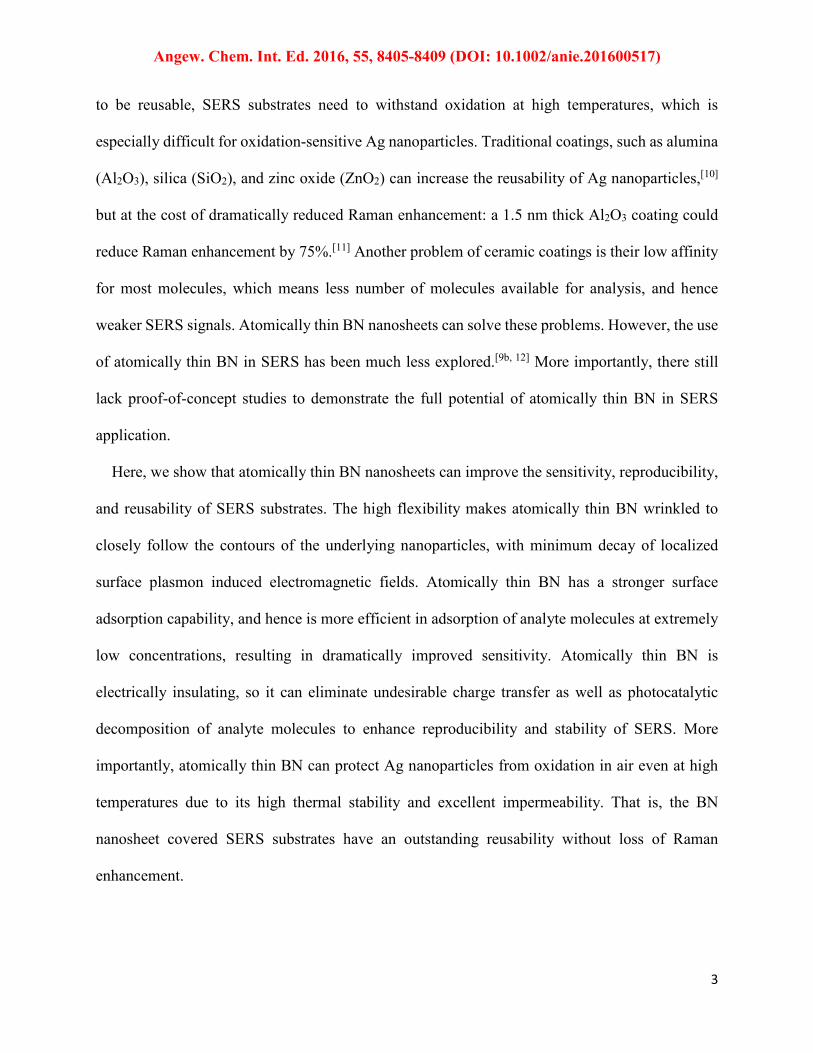
stronger surface adsorption capability of atomically thin BN. After the BN nanosheets of different
thicknesses immersed in R6G aqueous solution of 10-6 M for 1 min, the atomic force microscopy
(AFM) images (Figure 1a and b) show that the thickness increase due to R6G adsorption for all
BN nanosheets was the same, i.e. ~0.9 nm, corresponding to a monolayer of lying-down R6G
molecules, whose xanthene ring structures are parallel to BN surface due to strong π-π
interactions.[14] However, the amount of the adsorbed molecules decreased with the increase of
BN’s thickness. Such intriguing phenomenon can be better seen in Figure 1c, where the surface of
all the BN nanosheets were adjusted to the same color (i.e. AFM height) so that their coverage of
R6G could be directly compared. The bilayer (2L) BN nanosheet was almost completely covered
by R6G molecules, whereas the surface of a bulk hBN (~50 nm thick) adsorbed much less
molecules. The adsorption coverage estimated from the AFM images[15] is 90% on 2L BN, ~70%
on 3-6L BN, and less than 40% on the bulk BN, respectively (Figure 1d). Thus, the thinner the BN
nanosheet, the higher the surface adsorption. According to our recent investigation, such
phenomenon can be ascribed to conformational change in atomically thin nanosheets, which
increases adsorption energy and efficiency (see Supporting Information for Review ONLY).
Conformational change often happens to soft adsorbates, such as macromolecules and
biomolecules, and has been rarely observed on adsorbent. However, atomically thin BN
nanosheets are highly flexible, so that adsorbent, i.e. atomically thin BN, instead of adsorbate,
R6G, experienced conformational change in the current case. Bulk hBN crystals are not able to
4
Angew. Chem. Int. Ed. 2016, 55, 8405-8409 (DOI: 10.1002/anie.201600517)
perform conformational change, so they have worse adsorption performance than atomically thin
BN nanosheets.
Figure 1. AFM images of BN nanosheets before (a) and after (b) R6G adsorption; (c)
normalized AFM images with the surface of BN of different thicknesses adjusted to the same
height to reveal the different coverage of adsorbed R6G molecules under the same adsorption
condition; (d) estimated percentages of coverage v.s. BN thickness. Scale bars 2 µm.
The unique adsorption behavior and superior adsorption performance of atomically thin BN can
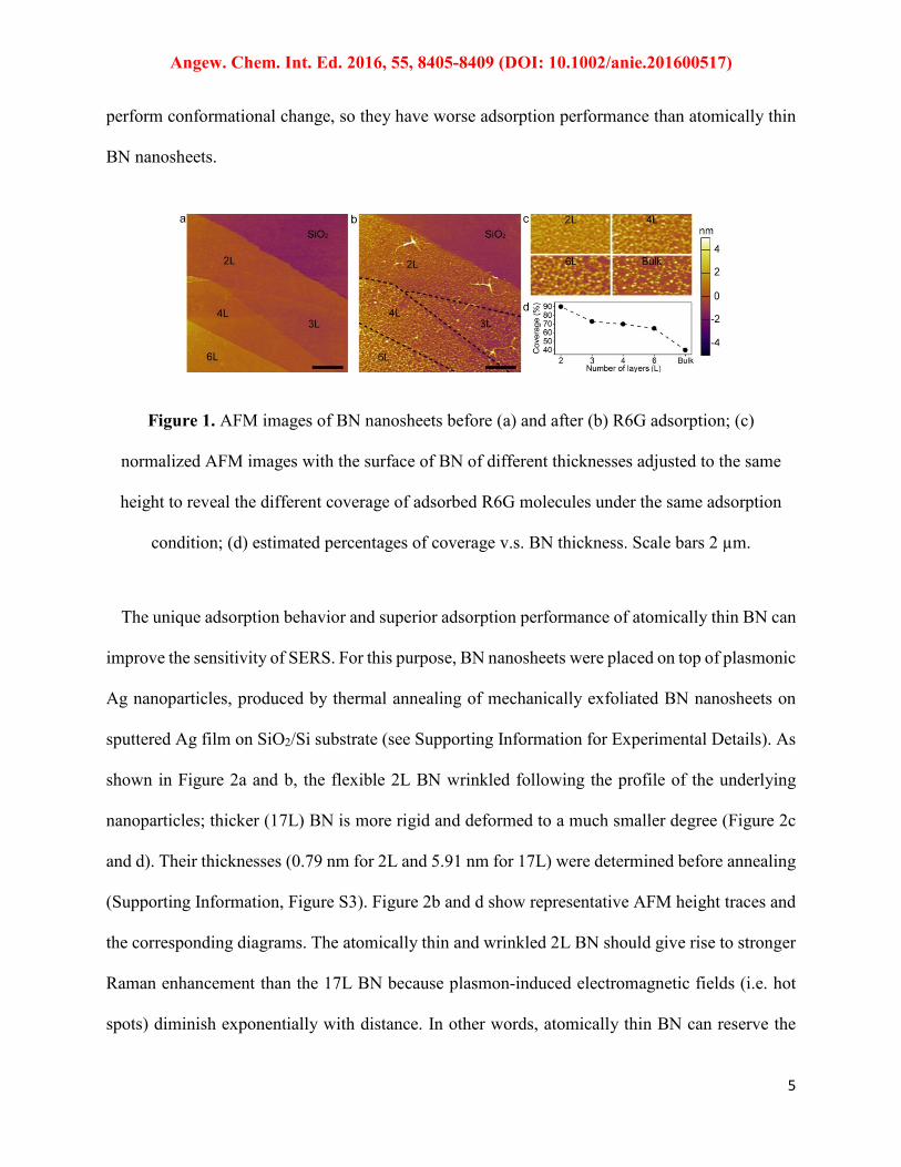
improve the sensitivity of SERS. For this purpose, BN nanosheets were placed on top of plasmonic
Ag nanoparticles, produced by thermal annealing of mechanically exfoliated BN nanosheets on
sputtered Ag film on SiO2/Si substrate (see Supporting Information for Experimental Details). As
shown in Figure 2a and b, the flexible 2L BN wrinkled following the profile of the underlying
nanoparticles; thicker (17L) BN is more rigid and deformed to a much smaller degree (Figure 2c
and d). Their thicknesses (0.79 nm for 2L and 5.91 nm for 17L) were determined before annealing
(Supporting Information, Figure S3). Figure 2b and d show representative AFM height traces and
the corresponding diagrams. The atomically thin and wrinkled 2L BN should give rise to stronger
Raman enhancement than the 17L BN because plasmon-induced electromagnetic fields (i.e. hot
spots) diminish exponentially with distance. In other words, atomically thin BN can reserve the
5
Angew. Chem. Int. Ed. 2016, 55, 8405-8409 (DOI: 10.1002/anie.201600517)
plasmonic hot spots. Note that the diameter and distribution of Ag nanoparticles with and without
BN coverage are similar (see Supporting Information, Figure S4), and according to our previous
study, the dielectric contant of BN nanosheets of differnt thicknesses is quite close.[16]
Figure 2. AFM images of Ag nanoparticles covered by 2L (a) and 17L (c) BN; (b) and (d) are
the height traces and schematic diagrams corresponding to the dotted lines in (a) and (c); (e)
SERS spectra of R6G (10 nM) from 2L, 17L and bulk BN, as well as the Ag/SiO2 substrate by
adsorption method, and # represents the Raman G band (E2g mode) of bulk hBN.
The sensitivity of the SERS substrates veiled by BN nanosheets of different thicknesses and a
bare Ag substrate was tested by immersing in 10-8 M aqueous solution of R6G. As expected, the
Raman features of R6G were most prominent from the 2L BN covered Ag nanoparticles (2L/Ag),
and the signal attenuated with the increase of BN thickness (Figure 2e). The bare Ag nanoparticles
on SiO2/Si substrate (Ag/SiO2), on the other hand, showed no Raman signature of R6G at either
10-8 or 10-7 M (Figure 2e and Supporting Information, Figure S5). That is, the 2L BN increased
the sensitivity of the SERS substrates by more than two orders of magnitude. The much better
6
Angew. Chem. Int. Ed. 2016, 55, 8405-8409 (DOI: 10.1002/anie.201600517)
enhancement from the atomically thin BN covered SERS substrate can be largely attributed to the
aforementioned two reasons: (1) atomically thin BN nanosheets are more efficient in capture of
analyte molecules, and (2) better reserved Raman hot spots due to their atomic thickness and
wrinkles. Between these two causes, the first one played a decisive role because 1) the
enhancement factors for these samples are close (see Supporting Information); 2) theoretically, the
Ag/SiO2 substrate should have the strongest electromagnetic field but showed no meaningful
signal due to its low affinity for aromatic molecules, whereas Bulk/Ag still showed weak Raman
peaks of R6G (Figure 2e). This was further confirmed by estimating the enhancement factors of
the different SERS substrates (see Supporting Information). Distinct from graphene which shows
strong Raman peaks, the Raman yield of atomically thin BN is so weak that its G band is not
visible. BN nanosheets can also improve SERS reproducibility and stability because they act as
dielectric separators to prevent undesired decomposition of analyte molecules caused by the
photocatalysis of Ag nanoparticles.
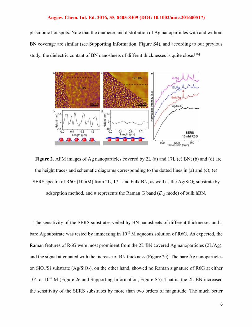
Figure 3. (a) Scanning electron microscopy (SEM) image of Ag particles covered by BN of
different thicknesses; (b) the corresponding Raman mapping from the squared area in (a) after
immersion in 10-6 M R6G solution for 1 h, where 0.0 means no intensity and 1.0 means the
strongest measured Raman peak at 612 cm-1.
7
Angew. Chem. Int. Ed. 2016, 55, 8405-8409 (DOI: 10.1002/anie.201600517)
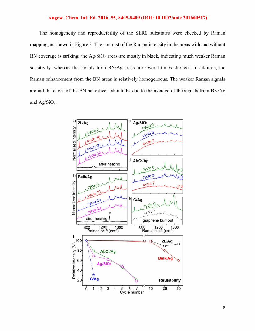
The homogeneity and reproducibility of the SERS substrates were checked by Raman
mapping, as shown in Figure 3. The contrast of the Raman intensity in the areas with and without
BN coverage is striking: the Ag/SiO2 areas are mostly in black, indicating much weaker Raman
sensitivity; whereas the signals from BN/Ag areas are several times stronger. In addition, the
Raman enhancement from the BN areas is relatively homogeneous. The weaker Raman signals
around the edges of the BN nanosheets should be due to the average of the signals from BN/Ag
and Ag/SiO2.
8

Angew. Chem. Int. Ed. 2016, 55, 8405-8409 (DOI: 10.1002/anie.201600517)
Figure 4. Reusability tests of different SERS substrates: (a) 2L BN covered Ag nanoparticles
(2L/Ag) for 30 cycles; (b) bulk BN on Ag nanoparticles (Bulk/Ag) for 30 cycles, where #
represents the G band of bulk hBN; (c) bare Ag particles on SiO2 without BN protection
(Ag/SiO2) for 7 cycles; (d) ~1 nm thick ALD Al2O3 on Ag nanoparticles (Al2O3/Ag), and (e) 10
nm thick graphene on Ag nanoparticles (G/Ag) for 1 cycle, where * indicates the G band of
graphite. (f) Summarized change of the Raman enhancement of these SERS substrates based on
the intensity of the 612 cm-1 peak. The black lines in (a) and (b) are Raman spectra of 2L/Ag and
Bulk/Ag after heating at 360 °C in air for 5 min. The dashed lines for G/Ag in (e) and (f) mean
the graphene completely oxidized and disappeared after the first cycle.
Atomically thin BN nanosheets also make SERS substrates highly reusable. Heating in air has
been found the most effective and efficient way to remove adsorbed organic molecules for reusable
SERS.[9a, 9b] As shown in our previous studies,[6c, 8] BN nanosheets are a promising barrier to
protect metals because of their excellent thermal stability, high impermeability, and absence of
galvanic corrosion. This means that the BN covered Ag-based SERS substrates can have a long
“shelf-time” without loss of sensitivity due to oxidation, and more importantly, be regenerated by
simply heating in air to burn off the adsorbed molecules and then reused. The reusability of 2L/Ag,
Bulk/Ag and Ag/SiO2 substrates for up to 30 cycles are shown in Figure 4a-c. In each cycle, the
substrate was heated at 360 °C in air, and then reused by immersion in R6G solution (10-6 M). The
Raman signal and reusability of Ag/SiO2 cannot be obtained at concentrations lower than 10-6 M.
After the heating/cleaning treatment, no Raman signal of R6G was present on both 2L/Ag and
Bulk/Ag samples, except a Si band at ~1000 cm-1 and/or G band of hBN at 1366 cm-1 (black spectra
9

Angew. Chem. Int. Ed. 2016, 55, 8405-8409 (DOI: 10.1002/anie.201600517)
in Figure 4a and b), implying effective removal of the analyte. After 30 cycles of reusability tests,
the Raman intensity and frequency of R6G from 2L/Ag remained essentially unchanged (Figure
4a), indicating that the Ag nanoparticles were not affected even after the repeated heating in air.
In comparison, the Raman enhancement from Bulk/Ag substrate slightly weakened with the
increase of cycle numbers (Figure 4b). This difference can be attributed to the different
morphologies of atomically thin and bulk hBN on Ag nanoparticles. Atomically thin BN
nanosheets are very flexible so that they wrinkle to better “seal” the underlying Ag nanoparticles
from air; whereas thick hBN was unable to deform much, and there existed a gap between thick
BN and SiO2 substrate where air can penetrate to oxidize the Ag nanoparticles. Figure 2a-d,
especially the lower diagrams, can be referred to visualize such difference. The Raman sensitivity
of the bare Ag nanoparticles without BN protection, in contrast, plummeted in the reusability tests
(Figure 4c). To better compare their different reusability, the Raman sensitivity of the three
substrates after the tests are summarized in Figure 4f. The 2L/Ag and Bulk/Ag substrates retained
~90% and ~60% of their SERS activity after 30 cycles, respectively. For Ag/SiO2, its plasmon
enhancement decreased to 70% after the first cycle and further reduced to 20% after 7 cycles.
Atomically thin BN also has a long-term protection on Ag nanoparticles: 2L/Ag kept 90% of its
Raman enhancement after exposure to ambient condition for 1 year; while the Ag/SiO2 totally lost
its enhancement (Supporting Information, Figure S7).
For comparison, we also tested the reusability of two representative coatings, namely Al2O3
and graphene, as both materials have been proposed as protective barriers for SERS substrates
with Ag nanoparticles.[4a, 10c] A 1.07 nm thick film (slightly thicker than 2L BN) of Al2O3 was
grown on Ag/SiO2 (Al2O3/Ag) by atomic layer deposition (ALD) (see Supporting Information,
Figure S8), which can produce highly dense and uniform thin films.[17] Al2O3/Ag showed Raman
10
Angew. Chem. Int. Ed. 2016, 55, 8405-8409 (DOI: 10.1002/anie.201600517)
enhancement almost 10 times weaker than 2L/BN mainly due to two reasons. First, Al2O3 has a
low affinity for R6G so that much less amounts of molecules can be adsorbed on the substrate.
Second, it was reported before that a 1.5 nm thick Al2O3 film can reduce the Raman enhancement
by more than 75%.[11] Moreover, the Al2O3 film showed almost no protection which could be due
to inevitable defects in the film (Figure 4d), and its enhancement dropped to 20% after 7 cycles of
reusability test, following a similar trend of Ag/SiO2 (green line in Figure 4f).
High-quality graphene of 10 nm was produced on Ag nanoparticles by mechanical exfoliation,
following the same synthesis route of BN/Ag. The SERS substrate of graphene covered Ag
nanoparticles (G/Ag) showed comparable Raman enhancement to that of Bulk/Ag because
graphene can also attract R6G via π-π interaction, but with lower background due to charge transfer
(Figure 4e).[2a, 18] The G band of graphene (labelled by *) is pronounced compared to the peaks
from R6G. The heating at 360 °C in air for 5 min (1 cycle) had disastrous effect on the Raman
enhancement of G/Ag with a drop to 30% of the initial signal strength (blue dashed line in Figure
4f). It was because the ~10 nm thick graphene burnt out after the heating treatment (see Supporting
Information, Figure S9), which dramatically decreased the amount of R6G molecules adsorbed on
bare Ag/SiO2 without graphene.
X-ray photoelectron spectroscopy (XPS) was used to analyze the oxidation levels of Ag
nanoparticles on these substrates after reusability tests (Figure 5). Ag nanoparticles protected by
BN nanosheets showed a dominating silver peak at 368.2 eV, indicating almost no increase of
silver oxide after 30 cycles of reusability tests; while Ag particles without protection of BN or
covered by the Al2O3 thin film showed a strong silver oxide peak at 367.6 eV,[19] suggesting ~50%
contents of oxide after reusability tests. These results further confirm that BN nanosheets are an
excellent material for reusable SERS devices.
11

Angew. Chem. Int. Ed. 2016, 55, 8405-8409 (DOI: 10.1002/anie.201600517)
Figure 5. XPS spectra of Ag particles with and without BN protection before and after
reusability tests.
In summary, atomically thin BN nanosheets can be used to fabricate highly sensitive,
reproducible, and reusable SERS substrates. They are efficient in adsorption of aromatic molecules
to improve Raman sensitivity especially at extremely low concentrations. The Raman
enhancement from such substrates was homogeneous and reproducible. Furthermore, BN
nanosheets could protect the Ag nanoparticles from oxidation even at high temperatures in air in
the long term so that excellent reusability was achieved. The proposed SERS substrate and
fabrication method can be easily scaled up using large-sized BN nanosheets grown by chemical
vapor deposition (CVD).[20] On the other hand, BN nanosheets can be also used to cover SERS
12

Angew. Chem. Int. Ed. 2016, 55, 8405-8409 (DOI: 10.1002/anie.201600517)
substrates produced from other methods, e.g. self-assembly, or other metal nanoparticles to
improve surface adsorption, reproducibility, and reusability.
Acknowledgements
L.H.Li thanks the financial support from the Australian Research Council under Discovery Early
Career Researcher Award (DE160100796), and Deakin University under Alfred Deakin Research
Postdoctoral Fellowship 2014, and Central Research Grants Scheme 2015. Y.Chen acknowledges
the funding support from the Australian Research Council under the Discovery project. This work
was performed in part at the Melbourne Centre for Nanofabrication (MCN).
Keywords: boron nitride nanosheets • surface enhanced Raman spectroscopy (SERS) • surface
adsorption • reusability
[1] a) S. Schlucker, Angew. Chem. Int. Ed. 2014, 53, 4756-4795; b) P. H. C. Camargo, M.
Rycenga, L. Au, Y. N. Xia, Angew. Chem. Int. Ed. 2009, 48, 2180-2184.
[2] a) X. Ling, L. M. Xie, Y. Fang, H. Xu, H. L. Zhang, J. Kong, M. S. Dresselhaus, J. Zhang, Z.
F. Liu, Nano Lett. 2010, 10, 553-561; b) X. Ling, J. Zhang, Small 2010, 6, 2020-2025; c) H.
H. Cheng, Y. Zhao, Y. Q. Fan, X. J. Xie, L. T. Qu, G. Q. Shi, ACS Nano 2012, 6, 2237-2244;
d) Z. Y. Zhang, Q. H. Liu, D. L. Gao, D. Luo, Y. Niu, J. Yang, Y. Li, Small 2015, 11, 3000-
3005.
13

Angew. Chem. Int. Ed. 2016, 55, 8405-8409 (DOI: 10.1002/anie.201600517)
[3] a) W. Xu, J. Xiao, Y. Chen, Y. Chen, X. Ling, J. Zhang, Adv. Mater. 2013, 25, 928-933; b)
W. Xu, X. Ling, J. Xiao, M. S. Dresselhaus, J. Kong, H. Xu, Z. Liu, J. Zhang, Proc. Natl.
Acad. Sci. U.S.A. 2012, 109, 9281-9286; c) Z. Zhang, F. G. Xu, W. S. Yang, M. Y. Guo, X.
D. Wang, B. L. Zhanga, J. L. Tang, Chem. Commun. 2011, 47, 6440-6442; d) P. Luo, C. Li,
G. Shi, Phys. Chem. Chem. Phys. 2012, 14, 7360-7366; e) J. Wang, X. Gao, H. Sun, B. Su, C.
Gao, Mater. Lett. 2016, 162, 142-145.
[4] a) X. Li, J. Li, X. Zhou, Y. Ma, Z. Zheng, X. Duan, Y. Qu, Carbon 2014, 66, 713-719; b) M.
Losurdo, I. Bergmair, B. Dastmalchi, T. H. Kim, M. M. Giangregroio, W. Y. Jiao, G. V.
Bianco, A. S. Brown, K. Hingerl, G. Bruno, Adv. Funct. Mater. 2014, 24, 1864-1878.
[5] a) D. Prasai, J. C. Tuberquia, R. R. Harl, G. K. Jennings, K. I. Bolotin, ACS Nano 2012, 6,
1102-1108; b) S. Chen, L. Brown, M. Levendorf, W. Cai, S.-Y. Ju, J. Edgeworth, X. Li, C.
W. Magnuson, A. Velamakanni, R. D. Piner, ACS Nano 2011, 5, 1321-1327.
[6] a) F. Zhou, Z. Li, G. J. Shenoy, L. Li, H. Liu, ACS Nano 2013, 7, 6939-6947; b) M. Schriver,
W. Regan, W. J. Gannett, A. M. Zaniewski, M. F. Crommie, A. Zettl, ACS Nano 2013, 7,
5763-5768; c) L. H. Li, T. Xing, Y. Chen, R. Jones, Adv. Mater. Interfaces 2014, 1, 1300132.
[7] L. Liu, S. M. Ryu, M. R. Tomasik, E. Stolyarova, N. Jung, M. S. Hybertsen, M. L. Steigerwald,
L. E. Brus, G. W. Flynn, Nano Lett. 2008, 8, 1965-1970.
[8] L. H. Li, J. Cervenka, K. Watanabe, T. Taniguchi, Y. Chen, ACS Nano 2014, 8, 1457-1462.
[9] a) P. Aldeanueva-Potel, E. Faoucher, R. A. Alvarez-Puebla, L. M. Liz-Marzan, M. Brust, Anal.
Chem. 2009, 81, 9233-9238; b) Y. Lin, C. E. Bunker, K. S. Fernando, J. W. Connell, ACS
Appl. Mater. Interfaces 2012, 4, 1110-1117; c) S. Faraji, K. L. Stano, O. Yildiz, A. Li, Y. Zhu,
P. D. Bradford, Nanoscale 2015, 7, 17038-17047.
14

Angew. Chem. Int. Ed. 2016, 55, 8405-8409 (DOI: 10.1002/anie.201600517)
[10] a) X. Y. Zhang, J. Zhao, A. V. Whitney, J. W. Elam, R. P. Van Duyne, J. Am. Chem. Soc.
2006, 128, 10304-10309; b) J. F. Li, Y. F. Huang, Y. Ding, Z. L. Yang, S. B. Li, X. S. Zhou,
F. R. Fan, W. Zhang, Z. Y. Zhou, D. Y. Wu, B. Ren, Z. L. Wang, Z. Q. Tian, Nature 2010,
464, 392-395; c) S. M. Mahurin, J. John, M. J. Sepaniak, S. Dai, Appl. Spectrosc. 2011, 65,
417-422; d) L. W. Ma, Y. Huang, M. J. Hou, Z. Xie, Z. J. Zhang, Sci. Rep. 2015, 5, 12890.
[11] J. A. Dieringer, A. D. McFarland, N. C. Shah, D. A. Stuart, A. V. Whitney, C. R. Yonzon, M.
A. Young, X. Y. Zhang, R. P. Van Duyne, Faraday Discuss. 2006, 132, 9-26.
[12] a) X. Ling, W. Fang, Y.-H. Lee, P. T. Araujo, X. Zhang, J. F. Rodriguez-Nieva, Y. Lin, J.
Zhang, J. Kong, M. S. Dresselhaus, Nano Lett. 2014, 14, 3033-3040; b) P. Dai, Y. Xue, X.
Wang, Q. Weng, C. Zhang, X. Jiang, D. Tang, X. Wang, N. Kawamoto, Y. Ide, Nanoscale
2015, 7, 18992-18997.
[13] a) T. Taniguchi, K. Watanabe, J. Cryst. Growth 2007, 303, 525-529; b) L. Li, L. H. Li, Y.
Chen, X. J. Dai, P. R. Lamb, B. M. Cheng, M. Y. Lin, X. Liu, Angew. Chem. Int. Ed. 2013,
52, 4212-4216.
[14] Q. Cai, L. H. Li, Y. Yu, Y. Liu, S. Huang, Y. Chen, K. Watanabe, T. Taniguchi, Phys. Chem.
Chem. Phys. 2015, 17, 7761-7766.
[15] L. H. Li, Y. Chen, Langmuir 2010, 26, 5135-5140.
[16] L. H. Li, E. J. Santos, T. Xing, E. Cappelluti, R. Roldán, Y. Chen, K. Watanabe, T. Taniguchi,
Nano Lett. 2014, 15, 218-223.
[17] M. Knez, N. Pinna, Wiley-VCH; John Wiley, Weinheim Chichester, 2011.
[18] E. S. Thrall, A. C. Crowther, Z. H. Yu, L. E. Brus, Nano Lett. 2012, 12, 1571-1577.
15
Angew. Chem. Int. Ed. 2016, 55, 8405-8409 (DOI: 10.1002/anie.201600517)
[19] a) E. Albiter, M. Valenzuela, S. Alfaro, G. Valverde-Aguilar, F. Martínez-Pallares, J. Saudi
Chem. Soc. 2015, 19, 563-573; b) E. Mysak, J. Smith, P. Ashby, J. Newberg, K. Wilson, H.
Bluhm, Phys. Chem. Chem. Phys. 2011, 13, 7554-7564.
[20] a) Y. M. Shi, C. Hamsen, X. T. Jia, K. K. Kim, A. Reina, M. Hofmann, A. L. Hsu, K. Zhang,
H. N. Li, Z. Y. Juang, M. S. Dresselhaus, L. J. Li, J. Kong, Nano Lett. 2010, 10, 4134-4139;
b) L. Song, L. J. Ci, H. Lu, P. B. Sorokin, C. H. Jin, J. Ni, A. G. Kvashnin, D. G. Kvashnin, J.
Lou, B. I. Yakobson, P. M. Ajayan, Nano Lett. 2010, 10, 3209-3215; c) Y. Gao, W. C. Ren,
T. Ma, Z. B. Liu, Y. Zhang, W. B. Liu, L. P. Ma, X. L. Ma, H. M. Cheng, ACS Nano 2013, 7,
5199-5206.
16
Angew. Chem. Int. Ed. 2016, 55, 8405-8409 (DOI: 10.1002/anie.201600517)
Supporting Information
1. Experimental details
Adsorption test. BN nanosheets were mechanically exfoliated from hBN single crystals on 90 nm
thick SiO2/Si substrate. The samples were heated at 350 °C in air for 1 h to remove tape residuals.
Atomically thin BN was located under an Olympus optical microscopy (BX51) equipped with a
DP71 camera, and the thickness was measured using a Cypher AFM (Asylum Research) in both
tapping and contact modes. The BN samples were immersed in R6G aqueous (Milli-Q water)
solution of 10-6 M for 1 min, then washed by water, and dried in argon (Ar) flow at room
temperature. The percentages of coverage was estimated using the histogram function in
Photoshop.
Preparation of SERS substrates. A ~10 nm thick layer of Ag film was deposited on SiO2 (140
nm)/Si wafer by sputtering method under Ar (pressure of ~5×10⁻² mbar) (SCD050, Bel-Tec). The
current was 40 mA, and the sputtering time ranged from 20 to 40s. Then, BN nanosheets were
mechanically exfoliated on the Ag film, following the aforementioned procedure. Subsequently,
heat treatment at 450 °C in Ar for 1 h transferred the Ag film to particles of suitable sizes and
distributions. The BN and graphene nanosheets were mechanically exfoliated following the same
procedure from hBN single crystals and highly ordered pyrolytic graphite (HOPG), respectively.
The SEM image of BN/Ag was taken using a Supra 55VP (Carl Zeiss) under 1.0 kV. The
deposition of the Al2O3 coatings was carried out in a Fiji F200 (Cambridge Nanotech) ALD reactor
using trimethyl aluminum (TMA) and water (H2O) as precursors. Ar was used as a carrier and
purging gas at a flow rate 20 sccm. The deposition temperature was 250 °C, and pressure was 200
mtorr. Each deposition cycle consisted of 0.02 s pulse of TMA, 10 s of Ar purge, 0.06 s pulse of
H2O, and finally 10 s Ar purge. For 1 nm coating, 11 cycles were conducted. The exact thickness
of the deposited layer (1.07 nm) was determined by a spectroscopic ellipsometer using a blank Si
wafer from the same ALD process.
Raman analysis. The BN veiled Ag particles on SiO2/Si substrate was soaked in 10-8 M R6G
(≥95%, Fluka) water solution for 1 h, washed with Milli-Q water to remove drops of R6G solution
on the substrate, and then dried under Ar flow at room temperature. The reusability was tested by
17

Angew. Chem. Int. Ed. 2016, 55, 8405-8409 (DOI: 10.1002/anie.201600517)
heating the substrate with R6G at 360 °C in air for 5 min and re-immersed in R6G solution of 10-
6 M for 1 h for up to 30 times. Raman spectra were collected by a Renishaw Raman microscope
equipped with a 514.5 nm laser. A 100× objective lens with a numerical aperture of 0.90 was used.
The laser power was ~2.5 mW. In mapping, the step size was 0.4 µm. All Raman spectrum were
calibrated with the Raman band of Si at 520.5 cm-1.
XPS analysis. The XPS data were collected in high vacuum (3 × 10⁻⁹ torr) using a Kratos AXIS
Ultra (DLD) spectrometer (Kratos Analytical Ltd, U.K.) equipped with a monochromated Al Kα
X-ray source. All XPS spectra were recorded at 0.1 eV/step and a pass energy of 20 eV. For
samples Ag/SiO2 before and after 30 cycles of reusability tests and Al2O3/Ag after 7 cycles, the
signals were collected from areas of 500 × 300 µm. For BN/Ag, the signals were from a square
area of 27 × 27 µm due to the relatively small sizes of BN nanosheets. The location was determined
by XPS mapping in N 1s region (Figure S1).
Figure S1. (a) XPS N1s mapping of BN nanosheets on Ag nanoparticles; (b) N1s mapping
overlay with optical image; (c) optical image of BN on silver film. The XPS spectrum was
collected form the square area (27 × 27 µm) in (b) and (c).
2. Optical microscopy images of BN nanosheets on Ag film and nanoparticles
Figure S2 shows the optical images of 1L, 2L, 17L BN nanosheets on Ag film before annealing
(a) and on Ag nanoparticles after annealing (b). It can be seen that the optical contrast for
atomically thin BN nanosheets became higher after annealing, and it was easier to locate them
during SERS measurements.
18
Angew. Chem. Int. Ed. 2016, 55, 8405-8409 (DOI: 10.1002/anie.201600517)
Figure S2. Optical microscopy images of exfoliated BN nanosheets on Ag/SiO2/Si substrate
before (a) and after (b) annealing in Ar gas at 450 ºC for 1 h.
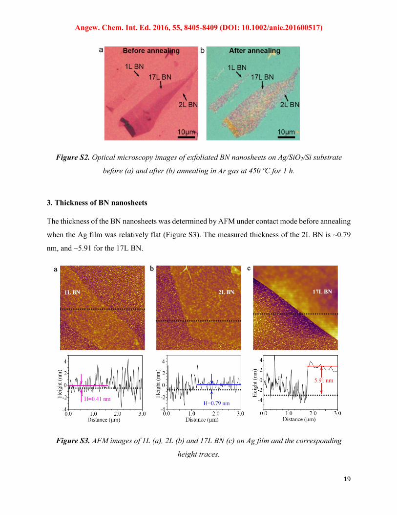
3. Thickness of BN nanosheets
The thickness of the BN nanosheets was determined by AFM under contact mode before annealing
when the Ag film was relatively flat (Figure S3). The measured thickness of the 2L BN is ~0.79
nm, and ~5.91 for the 17L BN.
Figure S3. AFM images of 1L (a), 2L (b) and 17L BN (c) on Ag film and the corresponding
height traces.
19
Angew. Chem. Int. Ed. 2016, 55, 8405-8409 (DOI: 10.1002/anie.201600517)
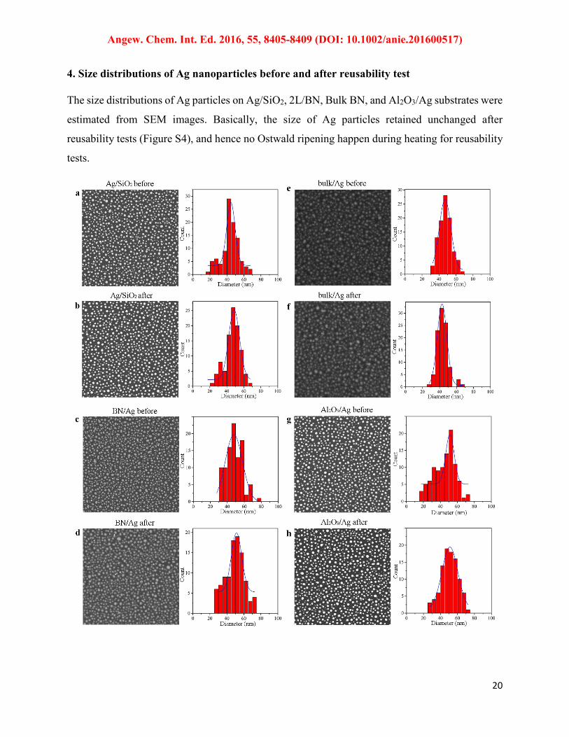
4. Size distributions of Ag nanoparticles before and after reusability test
The size distributions of Ag particles on Ag/SiO2, 2L/BN, Bulk BN, and Al2O3/Ag substrates were
estimated from SEM images. Basically, the size of Ag particles retained unchanged after
reusability tests (Figure S4), and hence no Ostwald ripening happen during heating for reusability
tests.
20
Angew. Chem. Int. Ed. 2016, 55, 8405-8409 (DOI: 10.1002/anie.201600517)
Figure S4. SEM images of Ag particles and the corresponding size distributions before and after
reusability tests: (a) and (b) Ag/SiO2; (c) and (d) BN/Ag; (e) and (f) Bulk/Ag; (g) and (h)
Al2O3/Ag.
5. Ag/SiO2 substrates show no Raman signal of 10-7 M R6G
As shown in Figure S5, the typical Raman peak of R6G at 610 cm-1 is undetectable on Ag/SiO2
substrate when the concentration is 10-7 M.
Figure S5. SERS spectra from Ag/SiO2 substrate after immersion in R6G solution (10-7 M) for 1
h.
6. Enhancement factors
The much stronger Raman signals from 2L/Ag substrates should be mainly due to the superior
surface adsorption of atomically thin BN towards R6G molecules. This was further confirmed by
estimating the enhancement factor (EF) of the different substrates using droplet method to deposit
R6G on substrates (1 droplet (20 µL) of R6G solution dripped on the substrates) because
immersion method could not quantitively reveal their Raman enhancements. The EFs for Ag/SiO2,
2L/Ag, and Bulk(0.5 µm thick BN)/Ag were close: 1.1×10⁵, 5.1×10⁵, and 0.9×10⁵, respectively.
The slightly higher EF from atomically thin BN covered Ag substrate was due to the better surface
adsorption of R6G on atomically thin BN due to π-π interactions, even though droplet instead of
immersion method was used. That is, with much suppressed effect of surface adsorption, the
enhancement by 2L/Ag was only 5 times of that by Ag/SiO2. Therefore, BN nanosheets showed
21

Angew. Chem. Int. Ed. 2016, 55, 8405-8409 (DOI: 10.1002/anie.201600517)
SERS signals 2 orders higher than Ag/SiO2 substrate can be mainly attributed to the effect of
surface adsorption.
7. R6G’s Raman background from BN/Ag as a function of laser energy
We tried 514.5, 632.8, and 785 nm lasers to test the effect of exciting laser energy on the
background of R6G on BN/Ag substrate. In these tests, the substrate was immersed in R6G water
solution (10-6 M) for 1 h.
Figure S6. Raman signals of R6G excited by lasers of different energies (a) 514.5 nm; (b) 632.8
nm; and (c) 785 nm.
8. Long-term protection of Ag nanoparticles by 2L BN nanosheets
The protection of 2L BN on Ag nanoparticles was tested under ambient condition over a period of
one year. It was found that 90% of the Raman enhancement from 2L/Ag substration was remained,
whereas bare Ag/SiO2 without BN protection totally lost Raman activity (Figure S7).
22

Angew. Chem. Int. Ed. 2016, 55, 8405-8409 (DOI: 10.1002/anie.201600517)
Figure S7. Raman enhancements of (a) 2L BN covered Ag nanoparticles and (b) bare Ag
nanoparticles on SiO2/Si without BN protection after exposed to ambient condition for 1 year.
This was tested by immersio the substrates in 10-6 M R6G solution for 1 h (c) Summary of the
change of Raman enhancement of the two substrates.
9. AFM images of the ALD Al2O3 film
The 1.07 nm Al2O3 film was deposited on Ag particles and SiO2/Si substrate by ALD method, and
Figure S8 shows AFM images of the film at different magnifications.
Figure S8. AFM images at different magnifications of the ~1 nm Al2O3 on SiO2/Si substrate.
10. Graphene burnt-out after 1 cycle of reusability test
Graphene was deposited on Ag film following the same procedure, and then the substrate was
heated at 450 ºC in Ar for 1 h to allow the formation of Ag particles. The AFM image of the just
23
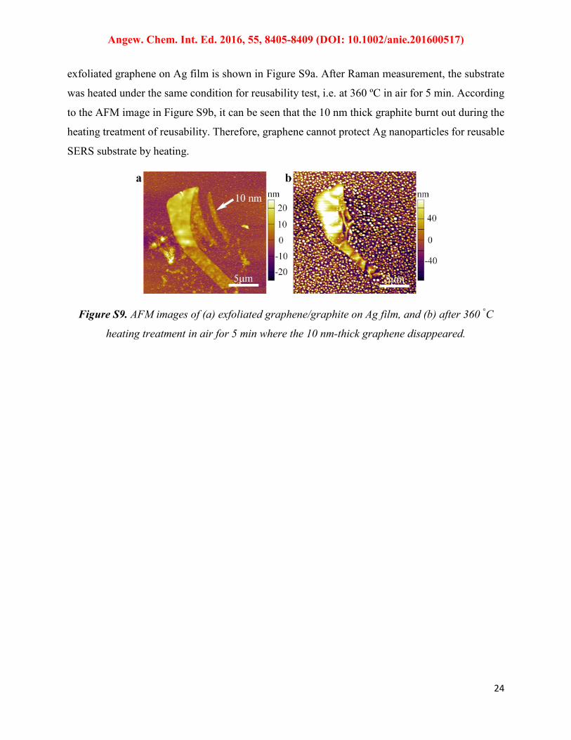
Angew. Chem. Int. Ed. 2016, 55, 8405-8409 (DOI: 10.1002/anie.201600517)
exfoliated graphene on Ag film is shown in Figure S9a. After Raman measurement, the substrate
was heated under the same condition for reusability test, i.e. at 360 ºC in air for 5 min. According
to the AFM image in Figure S9b, it can be seen that the 10 nm thick graphite burnt out during the
heating treatment of reusability. Therefore, graphene cannot protect Ag nanoparticles for reusable
SERS substrate by heating.
Figure S9. AFM images of (a) exfoliated graphene/graphite on Ag film, and (b) after 360 °C
heating treatment in air for 5 min where the 10 nm-thick graphene disappeared.
24