Boost DC-DC Converter Based Z-source Inverter with High ...
7
Gazi University Journal of Science GU J Sci 27(1):693-699 (2014) Boost DC-DC Converter Based Z-source Inverter with High Frequency Link Mohamad Reza BANAEI 1, ♠ , Ali Reza DEHGHANZADEH 1 , Aida BAGHBANY OSKOUEI 1 1 Azarbaijan Shahid Madani University, Electrical Engineering Department, Tabriz, IRAN Received: 19.11.2012 Revised: 17.08.2013 Accepted: 30.09.2013 ABSTRACT This paper proposes a new topology of DC-DC converters with high gain of boost. The suggested circuit consists of Z-source inverter, high frequency transformer and diode rectifier. In this topology the output voltage amplitude is not limited to DC voltage source and transformer turn ratio similar to traditional high frequency DC-DC converters and can be regulated with Z network shoot-through state control. Besides, it is more reliable against short circuit. By using high frequency modulation, the size of transformer is reduced and it is proper in isolation between high voltage and low voltage circuits. The performance of suggested inverter and switching algorithm are validated with simulation results using MATLAB/SIMULINK software. Key words: DC-DC Converter; high frequency transformer; Z-source inverter; boost factor 1. INTRODUCTION In several power conversion applications, it is required to convert a variable DC voltage source to a constant output dc voltage. This is performed by DC-DC converters [1-5].These converters are used in several applications such as regulated DC power supplies, renewable energy systems, electrical vehicles, distributed generation systems, and power factor Correction process. In some applications such as photovoltaic systems, boosting of DC voltage level with high gain is assumed. Recently, DC-DC boost converters based high switching frequency has received attention in research and renewable energies applications [1, 6-9]. Increased switching frequencies enable reduction in the numerical values and energy storage of the passive components that limit achievable transient response and account for the majority of converter size and cost. Furthermore, higher frequency can substantially improve transient performance and control bandwidth [1-5]. Based this theory, there are two main topologies for DC-DC converters: (1) High Frequency Resonant Boost Converter (2) isolated type. The isolated type of DC-DC converter utilizes high frequency (HF) transformer to increase DC voltage level. The isolated type is preferred when high voltage gain is required and it is proper for medium and high power applications [1-2]. The basic diagram of isolated type of DC-DC converter can be described as follows: first convert the DC voltage of source in the primary side of converter into high frequency signal through power electronic conversion, then couple the high frequency signal to the
Transcript of Boost DC-DC Converter Based Z-source Inverter with High ...

Gazi University Journal of Science
GU J Sci
27(1):693-699 (2014)
Boost DC-DC Converter Based Z-source Inverter with
High Frequency Link
Mohamad Reza BANAEI1, ♠
, Ali Reza DEHGHANZADEH 1
,
Aida BAGHBANY OSKOUEI1
1Azarbaijan Shahid Madani University, Electrical Engineering Department, Tabriz, IRAN
Received: 19.11.2012 Revised: 17.08.2013 Accepted: 30.09.2013
ABSTRACT
This paper proposes a new topology of DC-DC converters with high gain of boost. The suggested circuit
consists of Z-source inverter, high frequency transformer and diode rectifier. In this topology the output voltage amplitude is not limited to DC voltage source and transformer turn ratio similar to traditional high frequency
DC-DC converters and can be regulated with Z network shoot-through state control. Besides, it is more reliable
against short circuit. By using high frequency modulation, the size of transformer is reduced and it is proper in isolation between high voltage and low voltage circuits. The performance of suggested inverter and switching
algorithm are validated with simulation results using MATLAB/SIMULINK software.
Key words: DC-DC Converter; high frequency transformer; Z-source inverter; boost factor
1. INTRODUCTION
In several power conversion applications, it is required
to convert a variable DC voltage source to a constant
output dc voltage. This is performed by DC-DC
converters [1-5].These converters are used in several
applications such as regulated DC power supplies,
renewable energy systems, electrical vehicles,
distributed generation systems, and power factor
Correction process. In some applications such as
photovoltaic systems, boosting of DC voltage level with
high gain is assumed. Recently, DC-DC boost
converters based high switching frequency has received
attention in research and renewable energies
applications [1, 6-9]. Increased switching frequencies
enable reduction in the numerical values and energy
storage of the passive components that limit achievable
transient response and account for the majority of
converter size and cost. Furthermore, higher frequency
can substantially improve transient performance and
control bandwidth [1-5]. Based this theory, there are
two main topologies for DC-DC converters: (1) High
Frequency Resonant Boost Converter (2) isolated type.
The isolated type of DC-DC converter utilizes high
frequency (HF) transformer to increase DC voltage
level. The isolated type is preferred when high voltage
gain is required and it is proper for medium and high
power applications [1-2].
The basic diagram of isolated type of DC-DC converter
can be described as follows: first convert the DC
voltage of source in the primary side of converter into
high frequency signal through power electronic
conversion, then couple the high frequency signal to the

694 GU J Sci, 27(1):693-699 (2014)/ Mohamad Reza BANAEI ♠, Farhad Mohajel KAZEMI, Ali Reza DEHGHANZADEH
secondary side through a high frequency transformer,
finally revert the high frequency signal to the DC voltage level through rectifier [1].
In the applications that DC voltage of source is variable,
it is needed to regulate output DC voltage to setpoint
flexibility. In the conventional systems the other
converter as a DC–DC boost chopper is utilized to
regulate output DC voltage. In this paper, the Z-source
inverter is employed instead of DC–DC boost chopper.
The Z-source inverter utilizes Z-impedance network
between the DC source and inverter circuitry to achieve
boost operation. The voltage boost is achieved by
providing a shoot through state when both switches in
the same phase leg are on which is not possible with
traditional inverter topology. The Z-source inverters in
the comparing of traditional inverters are lower costs,
reliable, lower complexity and higher efficiency [10–14].
The voltage regulation of isolated high frequency DC-
DC converter is available by controlling of Z- source
boost factor. The proposed DC/DC converter is studied
in two modes: open loop and closed loop control scheme.
This paper is organized as follows. Section II introduces
Traditional isolated high frequency DC-DC converter.
Traditional Z-source inverter and the analyze of Z-
source inverter circuit is explained in section III.
Section IV presents the proposed topology. Simulation
results on proposed converter are provided in section V
and finally section VI draws the conclusions.
2. ISOLATED HIGH FREQUENCY DC-DC
CONVERTER
Fig. 1(a) shows the basic block diagram of the isolated
high frequency DC-DC converter. In this system, the
voltage of DC source is modulated with a converter to a
high-frequency square-wave and passed through a HF
transformer and again with a converter, it is
demodulated to DC form. The main function of the high
frequency transformer is voltage transformation and
isolation. Since the volume of the transformer is
inversely proportional to the frequency, the high
frequency transformer will be much smaller than the
conventional one [1].
In applications that voltage of DC source is variable, to
regulate output DC voltage, the DC-DC chopper can be utilized as Fig. 1(b).
The DC-DC chopper regulates DC voltage level to
reference level then the regulated DC voltage is
converted to a high frequency square-wave with
inverter. HF transformer couples the high frequency signal to the secondary side with turn ratio of N.
Figure 1. (a) Isolated high frequency transformer DC DC, (b)
regulated type of high frequency DC-DC.
3. Z-SOURCE INVERTER
The Z-source inverter structure is shown in Figure 2(a).
Assuming that the inductors L1 and L2 and capacitors
C1 and C2 have the same inductance (L) and
capacitance (C), respectively, the Z-source network
becomes symmetrical. The equivalent circuit of shoot-
trough state and non shoot-through state is shown in
Fig. 2(b) and Fig. 2(c), respectively. With the analyze of circuit Vin is obtained as [10, 14]:
dcsh
in V
T
TV )(
21
1
−
=
(1)
T
TB
sh21
1
−
=
(2)
Where T is period of switching and B is boost factor
and it is clear that 1≥B .
This configuration, unlike the traditional inverters, has
one extra zero state (or vector) when the terminals are
shorted through both the upper and lower devices of any
one leg or any two legs. So inverter is turned in to
shoot-through state when the output voltage level is traditional zero.
(a)

GU J Sci, 27(1):693-699 (2014)/ Mohamad Reza BANAEI, Farhad Mohajel KAZEMI, Ali Reza DEHGHANZADEH 695
(b)
(c)
Figure 2. Circuit diagram of (a) single phase Z-Source,
(b) Z-Source in shoot through state, (c) Z-Source in non
shoot through state.
4. PROPOSED STRUCTURE
Fig. 3 shows the proposed DC-DC converter based HF
transformer that utilizes Z-source. In this paper,
advanced DC-DC converter is suggested which
employs one dc input voltage source, Z-source inverter,
HF transformer and Diode rectifier .In Fig. 3, the input
DC voltage is modulated to high frequency square-wave
signal by Z-source inverter and the amplitude of square-
wave can be boosted related to DC voltage level of
source. HF square wave passes through HF transformer
with turn ratio of N. By neglecting the losses of HF
transformer, the HF transformer can be treated as a
proportional amplifier. The simplified model of the HF transformer is presented as:
i
i
ss V
N
NV =
(3)
Vi, Vs are the primary and secondary voltage amplitude
in HF transformer, respectively and N points to turn
ratio. By neglecting the on-stated voltage drop of
inverter power electronic switches, Vi equals Vin, therefore (3) can be written:
dc
i
ss V
N
NBV =
(4)
In secondary side of transformer, the HF square wave
is converted to DC voltage by rectifier and capacitor.
As compared to traditional inverters, the Z-source
inverter has an extra switching state: shoot-through.
During the shoot-through state, the output voltage of Z
network, Vin in Fig. 3 is zero. In this case, besides S1, S3
the other switches i.e. S2, S4 are turned on, while in non
shoot-through state only S1, S3 are turned on according to Table I.
Table I. Switchıng States And Output Voltage of Case Study
Voltage
Level
Output
Voltage
State ON Switches
Level 1
(active state)
1 Vin Non Shoot-Through
S1, S2
Level 0
(zero state)
0 (V) Non Shoot-Through
S1, S3 or S2, S4
Level 0
(zero state)
0 (V) Shoot-
Through S1, S4 or S2, S3
or S1, S2, S3, S4
Level -1
(active state)
-1 Vin Non Shoot-
Through S3, S4
In this paper, proposed topology is turned in to shoot-
through state when output voltage level is traditional
zero therefore some or all of the zero states are changed
to shoot-through. Table I shows the switching states
and output voltage of case study. As shown in Table I,
proposed topology is in the shoot-through state when S1
and S4 are on and the output voltage is zero similar to
non shoot-through level 0 state and other states are like traditional inverters switching algorithm.
As expressed in (1) and (2) the rate of voltage boost
depends on shoot-through time during switching period,
so by controlling shoot-through time a desirable DC output voltage can be obtained.
Relation between shoot-through and traditional zero
state is expressed as:
zs
sh
T
TD =
(5)
Where Tzs, Tsh are total zero state time and total shoot-
through time during switching period, T. It is
considered that by increasing D, boost factor B
increases, as a result the Z network output voltage Vin in
Fig. 3 increases and load voltage is controlled. In the
proposed topology the modulation index of the inverter
is kept constant and the output voltage of Z-source is
controlled by a shoot-through duty ratio, therefore the
THD is nearly constant for different boost ratio of output voltage.
As compared to structure shown in Fig. 1(b), the
proposed structure needs no switch in DC-DC part.
Besides, the suggested structure is more reliable against
short circuit. Switching algorithm of z-source inverter is based on the principle of phase-shifted PWM.

696 GU J Sci, 27(1):693-699 (2014)/ Mohamad Reza BANAEI ♠, Farhad Mohajel KAZEMI, Ali Reza DEHGHANZADEH
Figure 3. Proposed Structure
The technique of output feedback control is incorporated
to determine the switching actions of the z-source
inverter. Fig. 4 presents control circuit of proposed
structure in the closed loop scheme. The output load
voltage is compared to reference value. The PI controller
is applied to regulate the error between the load voltage
and its reference. Next the PI controller output is
compared to triangular waveform with high frequency
and square pulse with duty cycle of D is generated. The
frequency of triangular waveform is more than z-source inverter output frequency.
Figure 4. Control diagram of proposed structure in closed
loop scheme.
5. SIMULATION RESULTS
System shown in Fig. 3 has been modeled by
MATLAB/SIMULINK to study proposed topology.
The system parameters are listed in Table II
Table 2. Parameters of Case Study
10V DC Voltage Source
5 mH L1=L2
2300 µF C1=C2
R=100 Ω,L=22mH Load Impedance
0.0001 s T (switching frequency of
Z-source)
HF Transformer 1:10, 10kHZ
Three different duty cycles i.e. 0%, 25% and 50% have
been considered for generated pulse. Fig. 5 presents the
case study in D= 0%. In this duty cycle, according to (5)
zero states are not turned to shoot-through state, therefore
B=1. Fig. 5(a) presents the output voltage of Z network,
Vin which is about 10V. HF square-wave of primary and
secondary of transformer are shown in Fig 5(b) and (c)
respectively. Fig. 5(d) presents load DC voltage. As
shown in Fig. 5(d), desired DC level is 100.
Fig. 6 presents the case study in D= 25%. In this duty
cycle, according to (5) 25% of zero states time changed
to shoot-through states time. Fig. 6(a) presents the output
voltage of Z network, Vin which is about 12.5V. HF
square-wave of primary and secondary of transformer are
shown in Fig 6(b) and (c) respectively. Fig. 6(d) presents
load DC voltage. As shown in Fig. 6(d), desired DC level
is 125 v.
Fig. 7 presents the case study in D= 50%. In this duty
cycle, according to (5) half of zero states time changed to
shoot-through states time. Fig. 7(a) presents the output
voltage of Z network, Vin which is about 18.8V. HF
square-wave of primary and secondary of transformer are
shown in Fig 7(b) and (c) respectively. Fig. 7(d) presents
load DC voltage. As shown in Fig. 7(d), desired DC level
is 188 v.
S1 S3
S2 S4
HF
Transformer
L
O
A
D
Vi
Vs
L1
Vl
C1
Vin
L2
VC C2
Vdc

GU J Sci, 27(1):693-699 (2014)/ Mohamad Reza BANAEI, Farhad Mohajel KAZEMI, Ali Reza DEHGHANZADEH 697
(a)
(b)
(c)
(d)
Figure 5. Case 1: D=0 (a) Vin (b) HF square-wave of
primary side of transformer, Vi, (c) HF square-wave of
secondary side of transformer, Vs, Load voltage .
(a)
(b)
(c)
(d)
Figure 6. Case 2: D=25% (a) Vin (b) HF square-wave of
primary side of transformer, Vi, (c) HF square-wave of
secondary side of transformer, Vs, Load voltage .
698 GU J Sci, 27(1):693-699 (2014)/ Mohamad Reza BANAEI ♠, Farhad Mohajel KAZEMI, Ali Reza DEHGHANZADEH
(a)
(b)
(c)
(d)
Figure 7. Case 3: D=50% (a) Vin (b) HF square-wave of
primary side of transformer, Vi, (c) HF square-wave of
secondary side of transformer, Vs, Load voltage .
To study the advantages of proposed DC-DC converter in
the closed loop control scheme, the suggested structure is
modeled based control scheme as Fig. 4. Sudden
variation in the reference value of load voltage is
occurred. The reference value is changed from 120v to
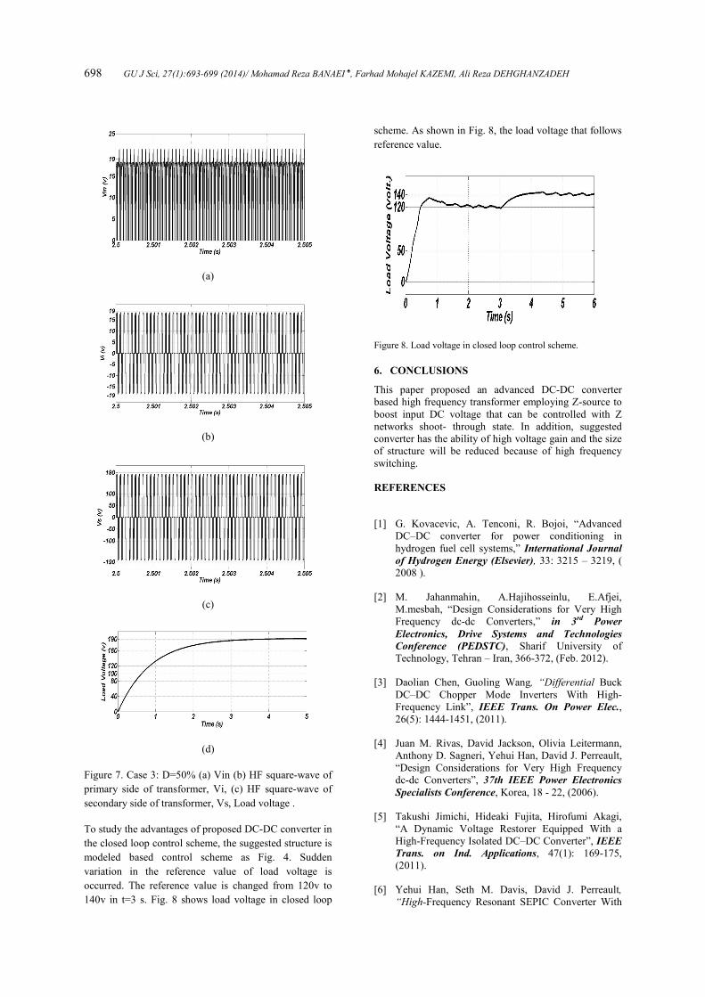
140v in t=3 s. Fig. 8 shows load voltage in closed loop
scheme. As shown in Fig. 8, the load voltage that follows
reference value.
Figure 8. Load voltage in closed loop control scheme.
6. CONCLUSIONS
This paper proposed an advanced DC-DC converter
based high frequency transformer employing Z-source to
boost input DC voltage that can be controlled with Z
networks shoot- through state. In addition, suggested
converter has the ability of high voltage gain and the size
of structure will be reduced because of high frequency
switching.
REFERENCES
[1] G. Kovacevic, A. Tenconi, R. Bojoi, “Advanced
DC–DC converter for power conditioning in
hydrogen fuel cell systems,” International Journal
of Hydrogen Energy (Elsevier), 33: 3215 – 3219, (
2008 ).
[2] M. Jahanmahin, A.Hajihosseinlu, E.Afjei,
M.mesbah, “Design Considerations for Very High
Frequency dc-dc Converters,” in 3rd Power
Electronics, Drive Systems and Technologies
Conference (PEDSTC), Sharif University of
Technology, Tehran – Iran, 366-372, (Feb. 2012).
[3] Daolian Chen, Guoling Wang, “Differential Buck
DC–DC Chopper Mode Inverters With High-
Frequency Link”, IEEE Trans. On Power Elec.,
26(5): 1444-1451, (2011).
[4] Juan M. Rivas, David Jackson, Olivia Leitermann,
Anthony D. Sagneri, Yehui Han, David J. Perreault,
“Design Considerations for Very High Frequency
dc-dc Converters”, 37th IEEE Power Electronics
Specialists Conference, Korea, 18 - 22, (2006).
[5] Takushi Jimichi, Hideaki Fujita, Hirofumi Akagi,
“A Dynamic Voltage Restorer Equipped With a
High-Frequency Isolated DC–DC Converter”, IEEE
Trans. on Ind. Applications, 47(1): 169-175,
(2011).
[6] Yehui Han, Seth M. Davis, David J. Perreault,
“High-Frequency Resonant SEPIC Converter With

GU J Sci, 27(1):693-699 (2014)/ Mohamad Reza BANAEI, Farhad Mohajel KAZEMI, Ali Reza DEHGHANZADEH 699
Wide Input and Output Voltage Ranges”, IEEE
Trans. on Power Elec., 27(1): 189-200, (2012).
[7] Haifeng Fan, Hui Li, “High-Frequency Transformer
Isolated Bidirectional DC–DC Converter Modules
With High Efficiency Over Wide Load Range for 20
kVA Solid-State Transformer”, IEEE Trans. on
Power Elec., 26(12): 3599-3608, (2011).
[8] D. Wang, C. Mao and J. Lu, “Modeling of electronic
power transformer and its application to power
system”, IET Gener. Transm. Distrib., 1(6): 887–
895, (2007).
[9] Shu Fan, Chengxiong Mao, Luonan Chen, “Optimal
coordinated PET and generator excitation control for
power systems”, Electrical Power and Energy
Systems, 28: 158–165, (2006).
[10] M.R. Banaei, A.R. Dehghanzadeh, E. Salary, H.
khounjahan, R. Alizadeh, "Z-source Based
Multilevel Inverter with Reduction of Switches",
IET Power Electronics, 5(3): 385-392, (2012).
[11] Miaosen Shen, Alan Joseph, Jin Wang, Fang Z.
Peng, Donald J. Adams, “Comparison of Traditional
Inverters and Z-source Inverter for Fuel Cell
Vehicles”, IEEE Trans. on Power Electronics,
22(4): 1453-1463,(2007).
[12] Miaosen Shen, Stefan Hodek, Fang Z.Peng,
“Control of the Z-Source Inverter for FCHEV with
the Connected to the Motor Neutral Point”, Power
Electronics Specialists Conference, PESC, (2007).
[13] Jin Wang, Fang Z.Peng, Leon M. Tolbert, Donald J.
Adams, “Maximum Constant Boost Control of the
Z- Source Inverter ”, Industry Application
Conference, 39 th Annual meeting Conference
Record, (2004).
[14] Amitava Das, Debasish Lahiri, A.K.Dhakar,
“Residential Solar Power Systems Using Z-Source
Inverter”, TENCON, IEEE Regional 10
Conference, (2008).