Board-level testing and IEEE1149.x Boundary Scan standard Artur Jutman [email protected] August 2010.
62
Board-level testing and Board-level testing and IEEE1149.x Boundary Scan IEEE1149.x Boundary Scan standard standard Artur Jutman Artur Jutman [email protected] [email protected] August 2010 August 2010
-
Upload
bennett-richardson -
Category
Documents
-
view
226 -
download
0
Transcript of Board-level testing and IEEE1149.x Boundary Scan standard Artur Jutman [email protected] August 2010.
Board-level testing and Board-level testing and IEEE1149.x Boundary Scan standardIEEE1149.x Boundary Scan standard
Artur JutmanArtur Jutman
[email protected]@ati.ttu.ee
August 2010August 2010

2
IEEE 1149.1 Boundary Scan IEEE 1149.1 Boundary Scan StandardStandard
• Board level testing challengesBoard level testing challenges
• Fault modeling at board level (digital)Fault modeling at board level (digital)
• Test generation for interconnect faultsTest generation for interconnect faults
• IEEE 1149.1 Boundary Scan StandardIEEE 1149.1 Boundary Scan Standard
• Application of Boundary ScanApplication of Boundary Scan
3
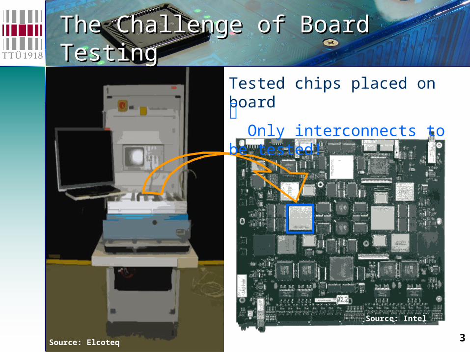
The Challenge of Board TestingThe Challenge of Board Testing
Tested chips placed on board
Only interconnects to be tested!
Source: Elcoteq
Source: Intel
4
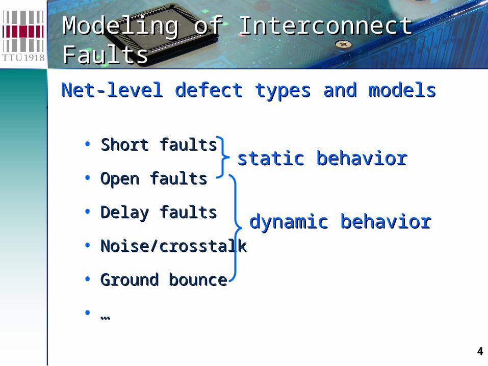
Modeling of Interconnect FaultsModeling of Interconnect Faults
• Short faultsShort faults
• Open faultsOpen faults
• Delay faultsDelay faults
• Noise/crosstalkNoise/crosstalk
• Ground bounceGround bounce
• ……
dynamic behaviordynamic behavior
static behaviorstatic behavior
Net-level defect types and models Net-level defect types and models
5
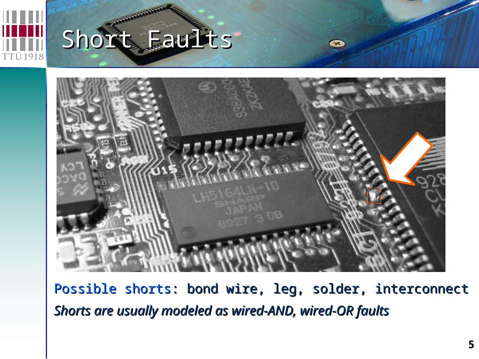
Short FaultsShort Faults
Possible shortsPossible shorts: bond wire, leg, solder, interconnect: bond wire, leg, solder, interconnect
Shorts are usually modeled as wired-AND, wired-OR faultsShorts are usually modeled as wired-AND, wired-OR faults
6
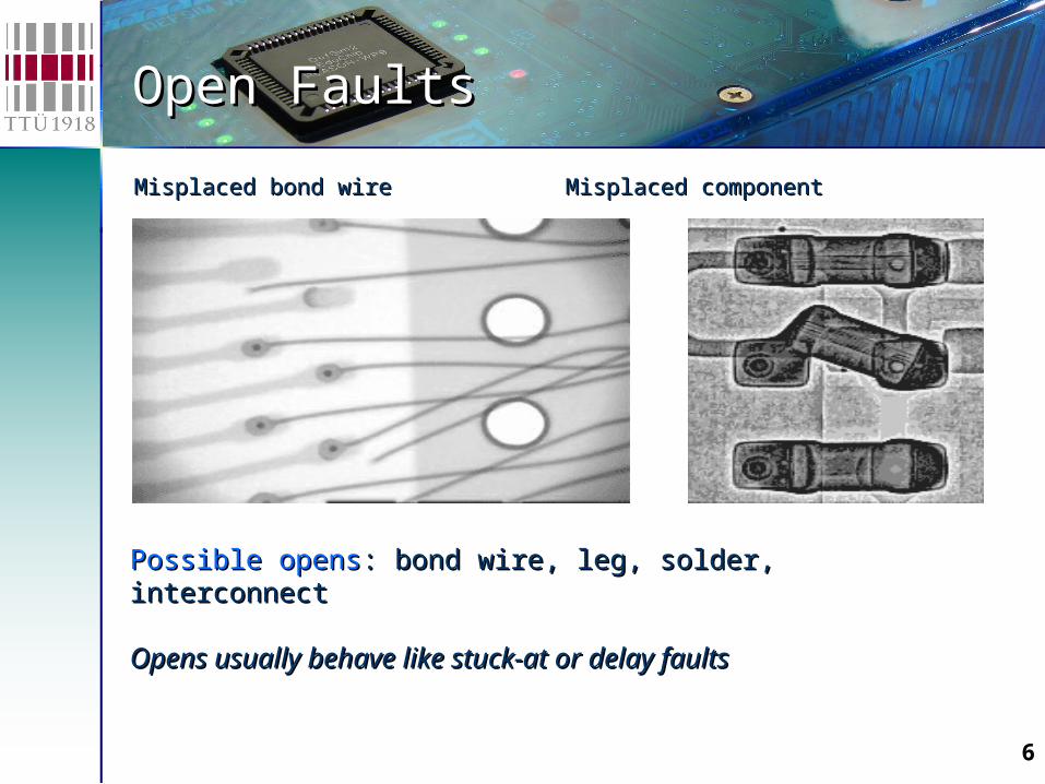
Open FaultsOpen Faults
Misplaced bond wireMisplaced bond wire Misplaced componentMisplaced component
Possible opensPossible opens: bond wire, leg, solder, interconnect: bond wire, leg, solder, interconnect
Opens usually behave like stuck-at or delay faultsOpens usually behave like stuck-at or delay faults
7
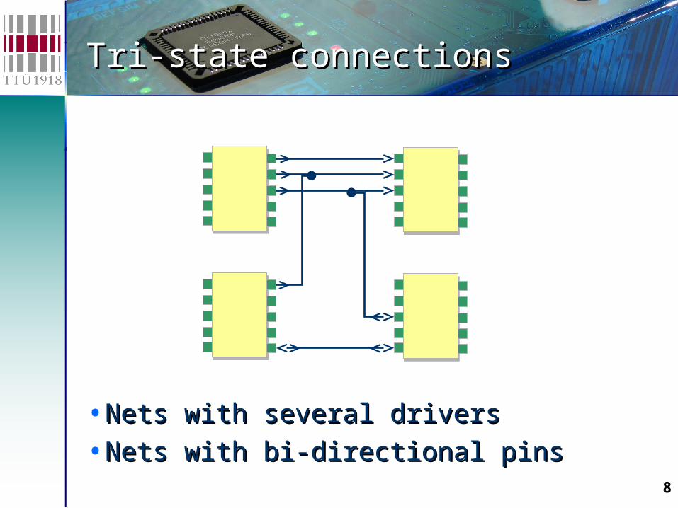
Tri-state connectionsTri-state connections
Main difference between logic circuits and Main difference between logic circuits and board-level systems is the way the board-level systems is the way the components are connected.components are connected.
Typical board-level interconnect uses Typical board-level interconnect uses tri-tri-state logicstate logic: logic-0, logic-1, and “high : logic-0, logic-1, and “high impedance” (switched off) state. Common impedance” (switched off) state. Common notation: notation: 0,1,Z0,1,Z..
There are special “enable” signals that There are special “enable” signals that control this additional state of the I/O pins.control this additional state of the I/O pins.
8
Tri-state connectionsTri-state connections
•Nets with several driversNets with several drivers
•Nets with bi-directional pinsNets with bi-directional pins
9
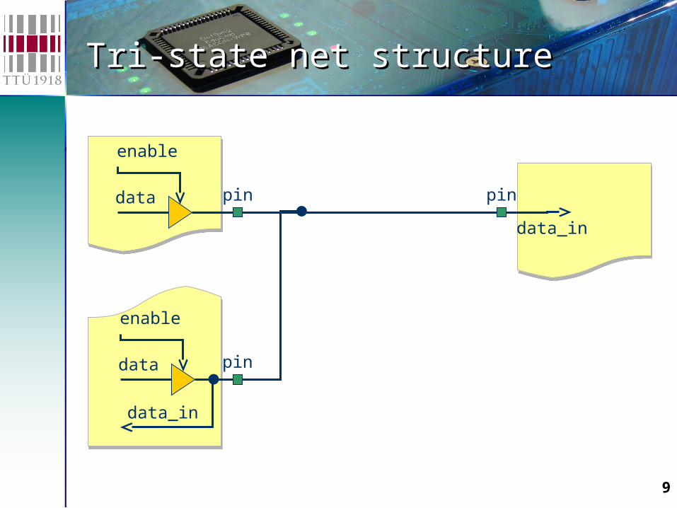
enable
data
Tri-state net structureTri-state net structure
pin
enable
data pin
data_in
pin
data_in
10
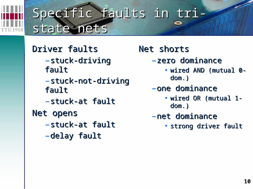
Specific faults in tri-state netsSpecific faults in tri-state nets
Driver faultsDriver faults–stuck-driving faultstuck-driving fault
–stuck-not-driving stuck-not-driving faultfault
–stuck-at faultstuck-at fault
Net opensNet opens–stuck-at faultstuck-at fault
–delay faultdelay fault
Net shortsNet shorts–zero dominancezero dominance
• wired AND (mutual 0-wired AND (mutual 0-dom.) dom.)
–one dominanceone dominance• wired OR (mutual 1-wired OR (mutual 1-
dom.) dom.)
–net dominancenet dominance• strong driver faultstrong driver fault
11
IEEE 1149.1 Boundary Scan IEEE 1149.1 Boundary Scan StandardStandard
• Board level testing challengesBoard level testing challenges
• Fault modeling at board level (digital)Fault modeling at board level (digital)
• Test generation for interconnect faultsTest generation for interconnect faults
• IEEE 1149.1 Boundary Scan StandardIEEE 1149.1 Boundary Scan Standard
• Application of Boundary ScanApplication of Boundary Scan
12
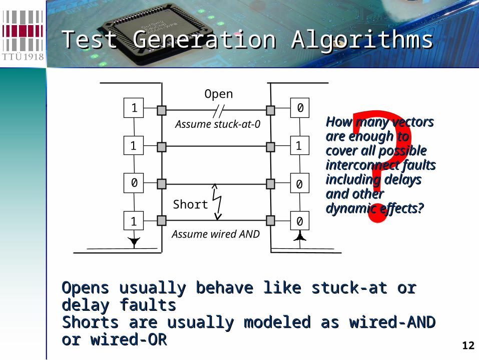
Test Generation AlgorithmsTest Generation Algorithms
0
0
1
0
1
1
1
0 How many How many vectors are vectors are enough to cover enough to cover all possible all possible interconnect interconnect faults including faults including delays and other delays and other dynamic effects?dynamic effects?
Opens usually behave like stuck-at or delay Opens usually behave like stuck-at or delay faultsfaultsShorts are usually modeled as wired-AND or Shorts are usually modeled as wired-AND or wired-ORwired-OR
Open
Assume stuck-at-0
Short
Assume wired AND
13
The Counting SequenceThe Counting Sequence
00
10
00
01
11
10
01
10
Kautz [1] showed in 1974 that a sufficient condition to detect Kautz [1] showed in 1974 that a sufficient condition to detect any pair of any pair of short circuitedshort circuited nets was that the serial codes must nets was that the serial codes must be unique for all nets. Therefore the test length is be unique for all nets. Therefore the test length is loglog22(N)(N)
What aboutWhat about
opens?opens?
Open
Assume stuck-at-0
Short
Assume wired AND
14
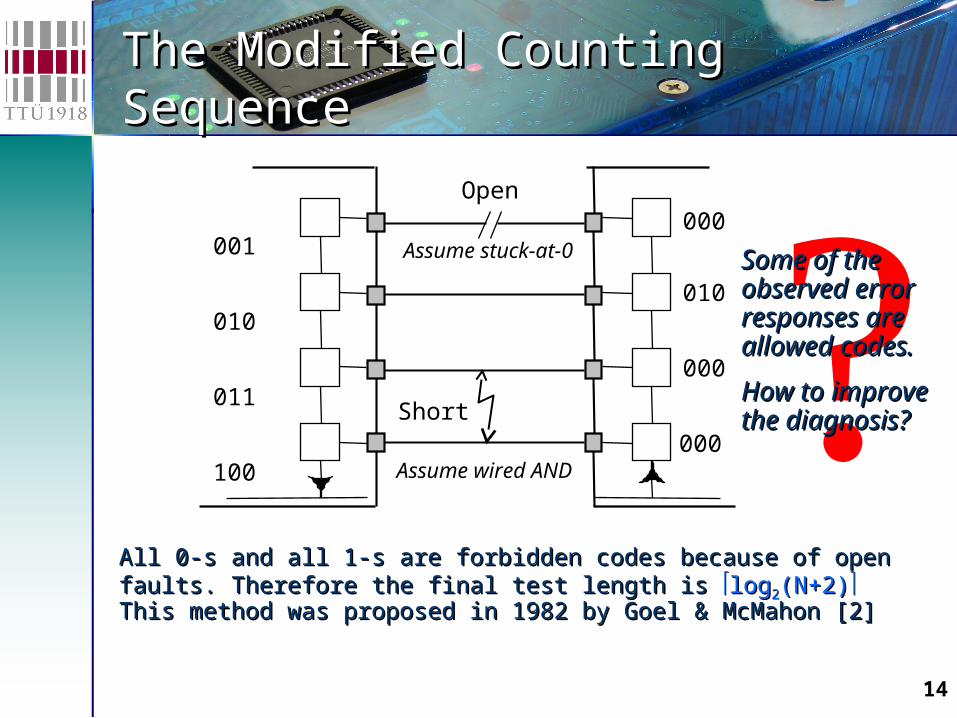
The Modified Counting The Modified Counting SequenceSequence
001
000
000
010
100
011
010
000
All 0-s and all 1-s are forbidden codes because of open All 0-s and all 1-s are forbidden codes because of open faults. Therefore the final test length is faults. Therefore the final test length is loglog22(N+2)(N+2)This method was proposed in 1982 by Goel & McMahon [2]This method was proposed in 1982 by Goel & McMahon [2]
Some of the Some of the observed error observed error responses are responses are allowed codes. allowed codes.
How to How to improve the improve the diagnosis?diagnosis?
Open
Assume stuck-at-0
Short
Assume wired AND

15
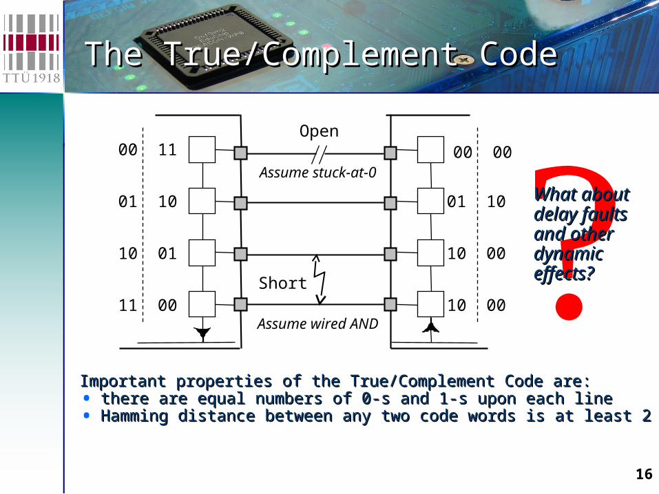
The True/Complement CodeThe True/Complement Code
00 11
10 00
00 00
01 10
11 00
10 01
01 10
10 00
To improve the diagnostic resolution Wagner proposed To improve the diagnostic resolution Wagner proposed the True/Complement Code in 1987 [3]. the True/Complement Code in 1987 [3]. The test length became equal The test length became equal 22loglog22(N)(N)
!All-0 and All-0 and all-1 all-1 codes are codes are not not forbidden forbidden anymore!anymore!
Open
Assume stuck-at-0
Short
Assume wired AND
16
The True/Complement CodeThe True/Complement Code
Important properties of the True/Complement Code are: Important properties of the True/Complement Code are: • there are equal numbers of 0-s and 1-s upon each linethere are equal numbers of 0-s and 1-s upon each line• Hamming distance between any two code words is at least 2Hamming distance between any two code words is at least 2
What about What about delay faults delay faults and other and other dynamic dynamic effects?effects?
00 11
10 00
00 00
01 10
11 00
10 01
01 10
10 00
Open
Assume stuck-at-0
Short
Assume wired AND
17
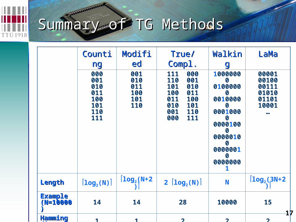
Summary of TG MethodsSummary of TG Methods
CountinCountingg
ModifieModifiedd
True/True/Compl.Compl.
WalkinWalkingg
LaMaLaMa
000001010011100101110111
001010011100101110
111 000110 001101 010100 011011 100010 101001 110000 111
1000000001000000001000000001000000001000000001000000001000000001
000010010000111010100110110001
…
LengthLength log2(N) log2(N+2) 2 log2(N) N log2(3N+2)
Example Example (N=10000)(N=10000) 14 14 28 10000 15
Hamming Hamming distancedistance 1 1 2 2 2
DefectsDefects Shorts ShortsOpens
ShortsOpens
/Delays/
ShortsOpens
/Delays/
ShortsOpens
Diagnostic Diagnostic PropertiesProperties Bad Bad Good Good Good
18
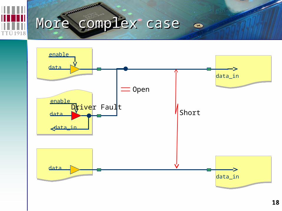
More complex caseMore complex case
enable
data
enable
data
data_in
data_in
data
data_in
Short
Open
Driver Fault
19
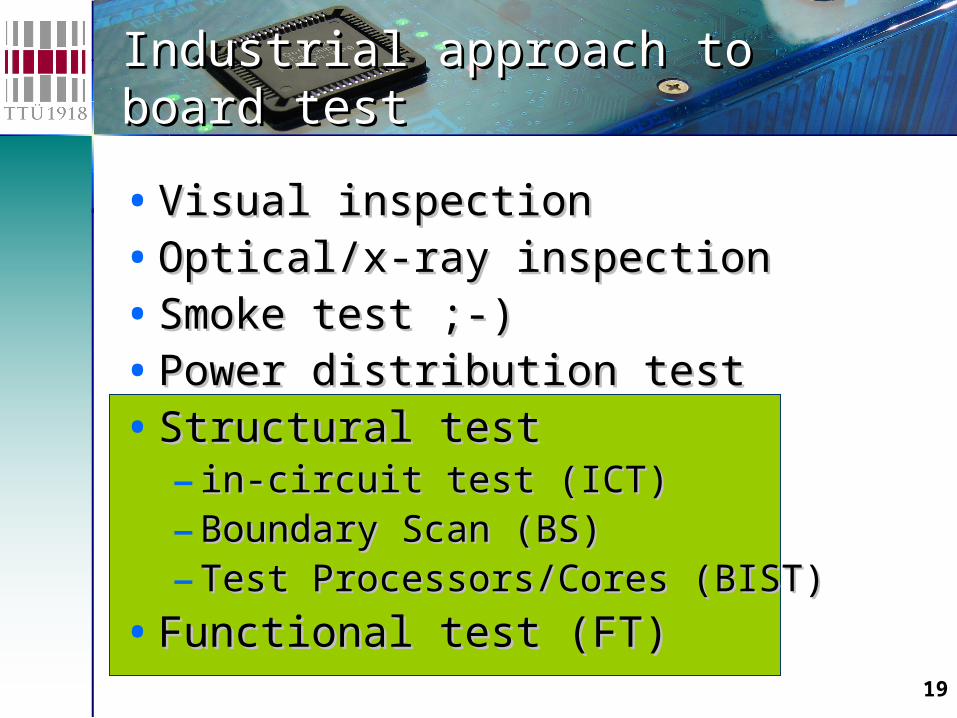
Industrial approach to board Industrial approach to board testtest
• Visual inspection Visual inspection • Optical/x-ray inspectionOptical/x-ray inspection• Smoke test ;-)Smoke test ;-)• Power distribution testPower distribution test• Structural testStructural test
– in-circuit test (ICT)in-circuit test (ICT)– Boundary Scan (BS)Boundary Scan (BS)– Test Processors/Cores (BIST)Test Processors/Cores (BIST)
• Functional test (FT)Functional test (FT)
20
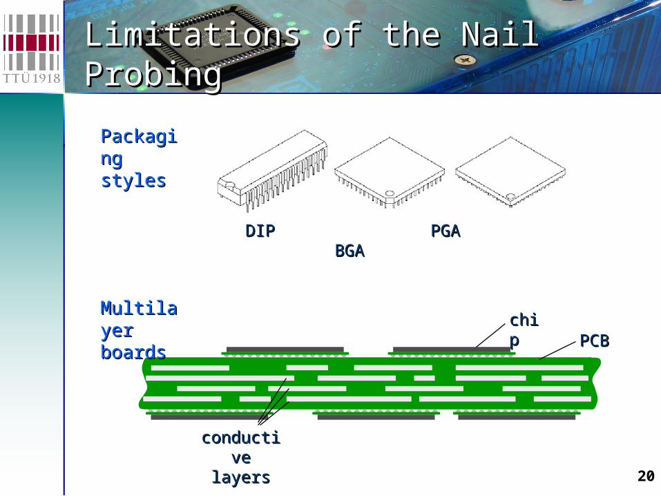
Limitations of the Nail ProbingLimitations of the Nail Probing
DIPDIP PGA BGA PGA BGA
PackaginPackaginggstylesstyles
MultilayeMultilayerrboardsboards
PCBPCBchichipp
conductivconductive layerse layers
21
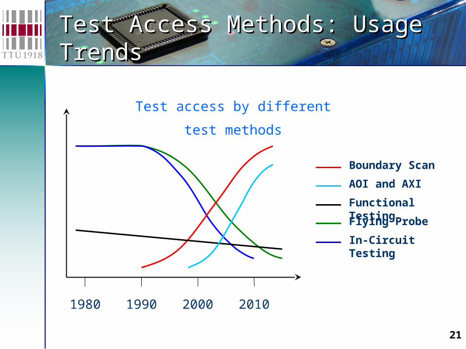
Test Access Methods: Usage Test Access Methods: Usage Trends Trends
1980 1990 2000 2010
Boundary Scan
AOI and AXI
Functional Testing
Flying Probe
In-Circuit Testing
Test access by different
test methods

22
IEEE 1149.1 Boundary Scan IEEE 1149.1 Boundary Scan StandardStandard
• Board level testing challengesBoard level testing challenges
• Fault modeling at board level (digital)Fault modeling at board level (digital)
• IEEE 1149.1 Boundary Scan StandardIEEE 1149.1 Boundary Scan Standard
• Test generation for interconnect faultsTest generation for interconnect faults
• Application of Boundary ScanApplication of Boundary Scan
23
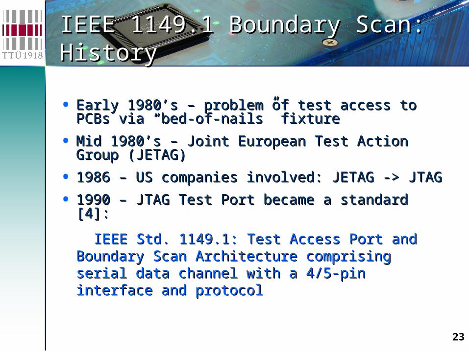
IEEE 1149.1 Boundary Scan: IEEE 1149.1 Boundary Scan: HistoryHistory
• Early 1980’s – problem of test access to PCBs Early 1980’s – problem of test access to PCBs via “bed-of-nails” fixturevia “bed-of-nails” fixture
• Mid 1980’s – Joint European Test Action Group Mid 1980’s – Joint European Test Action Group (JETAG)(JETAG)
• 1986 – US companies involved: JETAG -> JTAG1986 – US companies involved: JETAG -> JTAG
• 1990 – JTAG Test Port became a standard [4]:1990 – JTAG Test Port became a standard [4]:
IEEE Std. 1149.1: Test Access Port and IEEE Std. 1149.1: Test Access Port and Boundary Scan Architecture comprising serial Boundary Scan Architecture comprising serial data channel with a 4/5-pin interface and data channel with a 4/5-pin interface and protocolprotocol
24
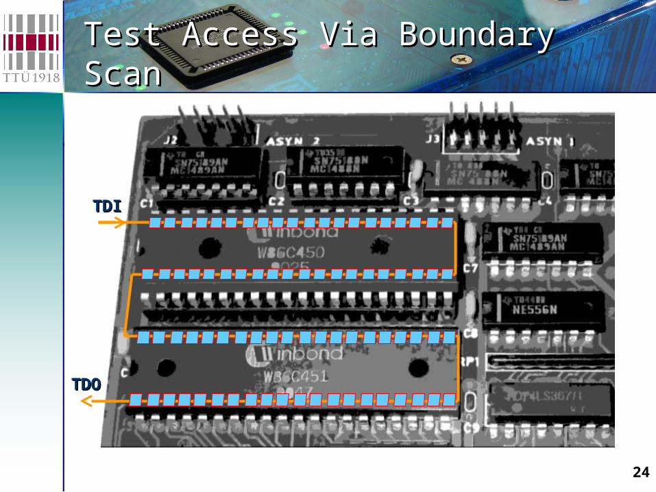
Test Access Via Boundary ScanTest Access Via Boundary Scan
TDOTDO
TDITDI
25
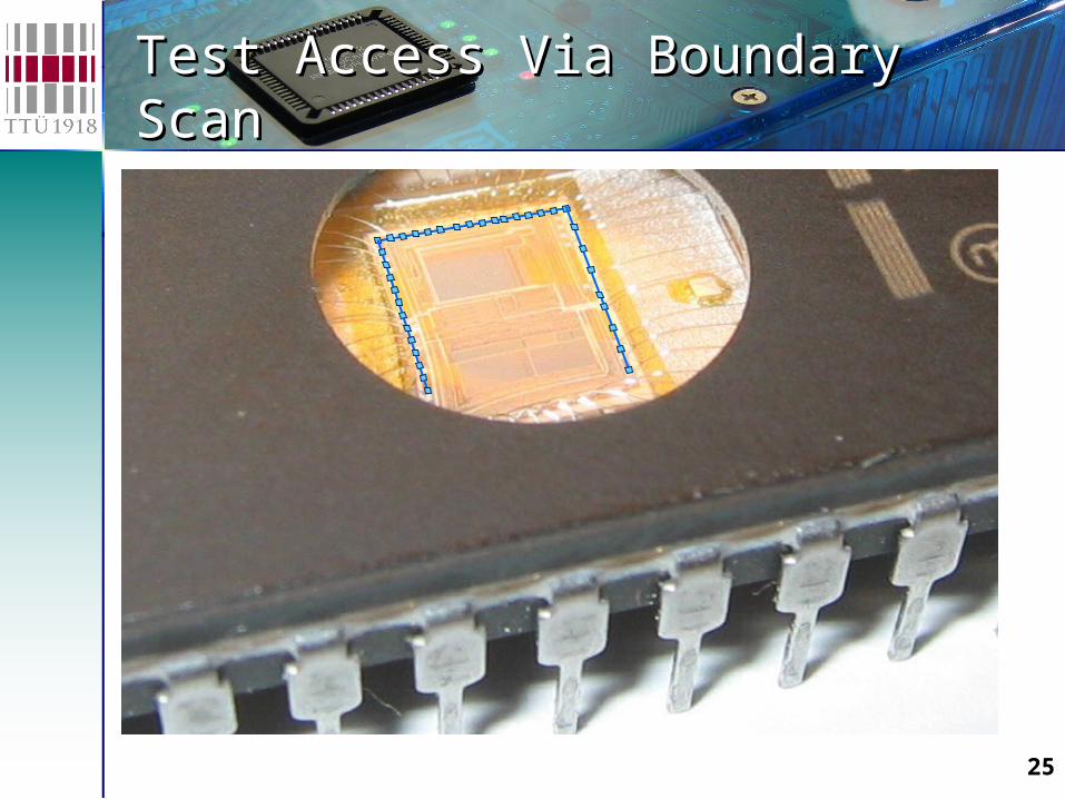
Test Access Via Boundary ScanTest Access Via Boundary Scan
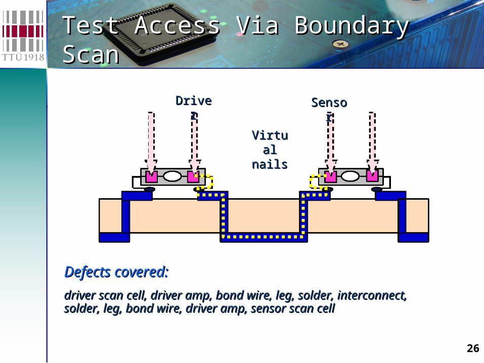
26
Test Access Via Boundary ScanTest Access Via Boundary Scan
Defects covered:Defects covered:
driver scan cell, driver amp, bond wire, leg, solder, driver scan cell, driver amp, bond wire, leg, solder, interconnect, solder, leg, bond wire, driver amp, sensor scan interconnect, solder, leg, bond wire, driver amp, sensor scan cellcell
DriverDriver SensorSensor
VirtuaVirtual nailsl nails
27
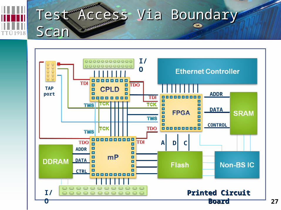
Test Access Via Boundary ScanTest Access Via Boundary Scan
Printed Circuit Printed Circuit BoardBoard
TAPport
I/O
I/O
DATA
ADDR
CONTROL
DATA
CTRL
ADDRA D C
28
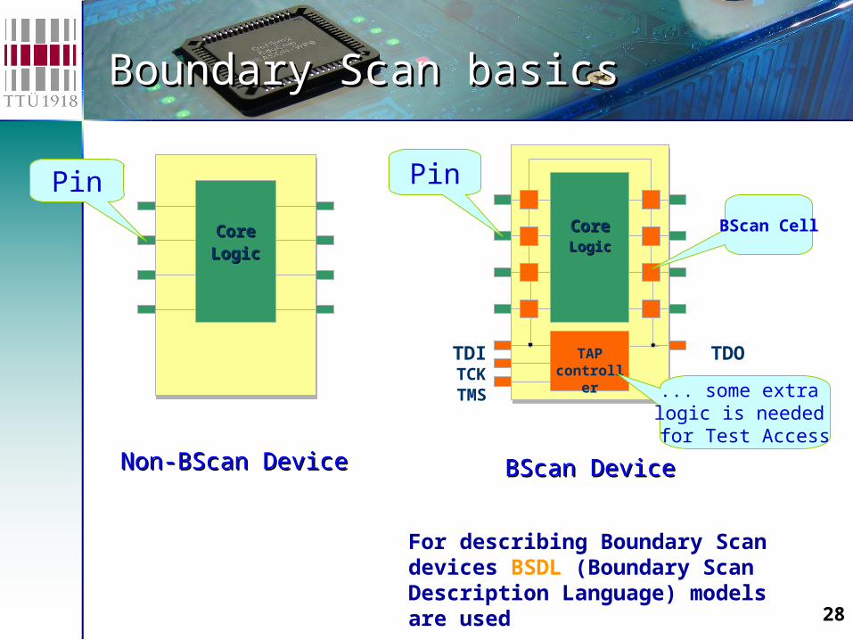
Boundary Scan basicsBoundary Scan basics
Non-BScan DeviceNon-BScan Device
CoreCore LogicLogic
Pin
BScan DeviceBScan Device
CoreCore LogicLogic
TAPcontroller
Pin
BScan Cell
TDO
TMS
TDITCK
... some extra logic is needed for Test Access
For describing Boundary Scan devices BSDL (Boundary Scan Description Language) models are used
29
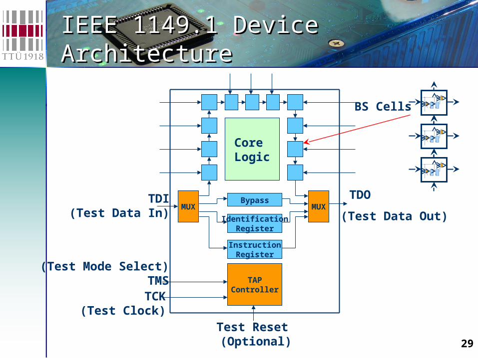
IEEE 1149.1 Device IEEE 1149.1 Device ArchitectureArchitecture
Core Logic
MUX MUXTDI
(Test Data In)
TDOBypass
IdentificationRegister
InstructionRegister
TAPController
(Test Data Out)
Test Reset (Optional)
(Test Mode Select)TMSTCK
(Test Clock)
BS Cells
30
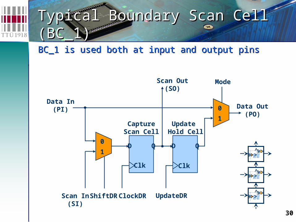
Typical Typical Boundary Scan CellBoundary Scan Cell (BC_1)(BC_1)BC_1 is used both at input and output pinsBC_1 is used both at input and output pins
0
1D Q
Clk
D Q
Clk
0
1
Data In(PI)
Scan Out(SO)
Mode
Data Out(PO)
CaptureScan Cell
Update Hold Cell
Scan In(SI)
ShiftDR ClockDR UpdateDR
31
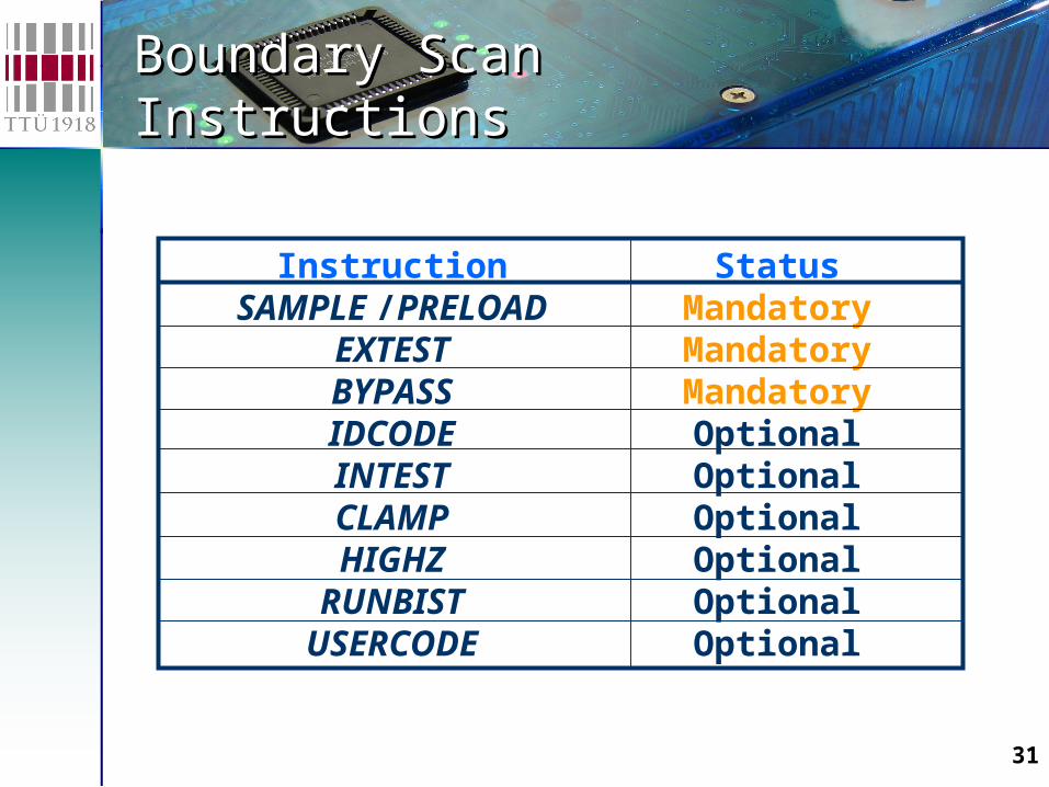
Boundary Scan InstructionsBoundary Scan Instructions
InstructionSAMPLE /PRELOAD
EXTESTBYPASSIDCODEINTESTCLAMPHIGHZ
RUNBISTUSERCODE
StatusMandatoryMandatoryMandatoryOptionalOptionalOptionalOptionalOptionalOptional
32
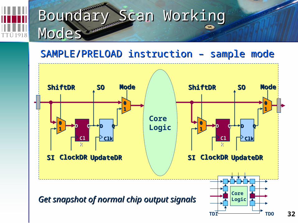
Boundary Scan Working ModesBoundary Scan Working Modes
SAMPLE/PRELOAD instruction – sample modeSAMPLE/PRELOAD instruction – sample mode
Get snapshot of normal chip output signalsGet snapshot of normal chip output signals
0011
D QD Q
ClkClk ClkClk
SOSO ModeModeShiftDRShiftDR
ClockDRClockDR UpdateDRUpdateDRSISI
0011
D QD Q0011
D QD Q
ClkClk ClkClk
SOSO ModeModeShiftDRShiftDR
ClockDRClockDR UpdateDRUpdateDRSISI
0011
D QD QCore Logic
Core Logic
TDOTDI
Get snapshot of normal chip output signalsGet snapshot of normal chip output signals
33
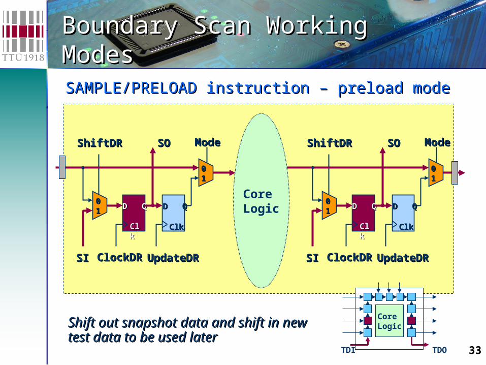
Boundary Scan Working ModesBoundary Scan Working Modes
SAMPLE/PRELOAD instruction – preload mode SAMPLE/PRELOAD instruction – preload mode
Shift out snapshot data and shift in new test data to be used latShift out snapshot data and shift in new test data to be used later
0011
D QD Q
ClkClk ClkClk
SOSO ModeModeShiftDRShiftDR
ClockDRClockDR UpdateDRUpdateDRSISI
0011
D QD Q0011
D QD Q
ClkClk ClkClk
SOSO ModeModeShiftDRShiftDR
ClockDRClockDR UpdateDRUpdateDRSISI
0011
D QD QCore Logic
Core Logic
TDOTDI
Shift out snapshot data and shift in Shift out snapshot data and shift in new test data to be used laternew test data to be used later
34
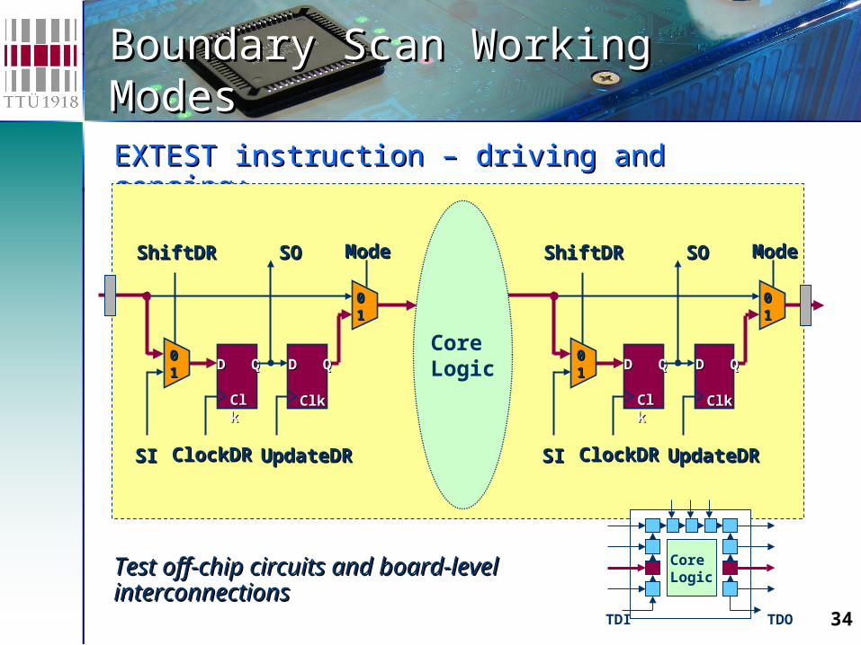
Boundary Scan Working ModesBoundary Scan Working Modes
EEXTESTXTEST instruction instruction – driving and sensing:– driving and sensing:
Test off-chip circuits and board-level interconnectionsTest off-chip circuits and board-level interconnections
0011
D QD Q
ClkClk ClkClk
SOSO ModeModeShiftDRShiftDR
ClockDRClockDR UpdateDRUpdateDRSISI
0011
D QD QCore Logic
0011
D QD Q
ClkClk ClkClk
SOSO ModeModeShiftDRShiftDR
ClockDRClockDR UpdateDRUpdateDRSISI
0011
D QD Q
Core Logic
TDOTDI
Test off-chip circuits and board-level Test off-chip circuits and board-level interconnectionsinterconnections
35
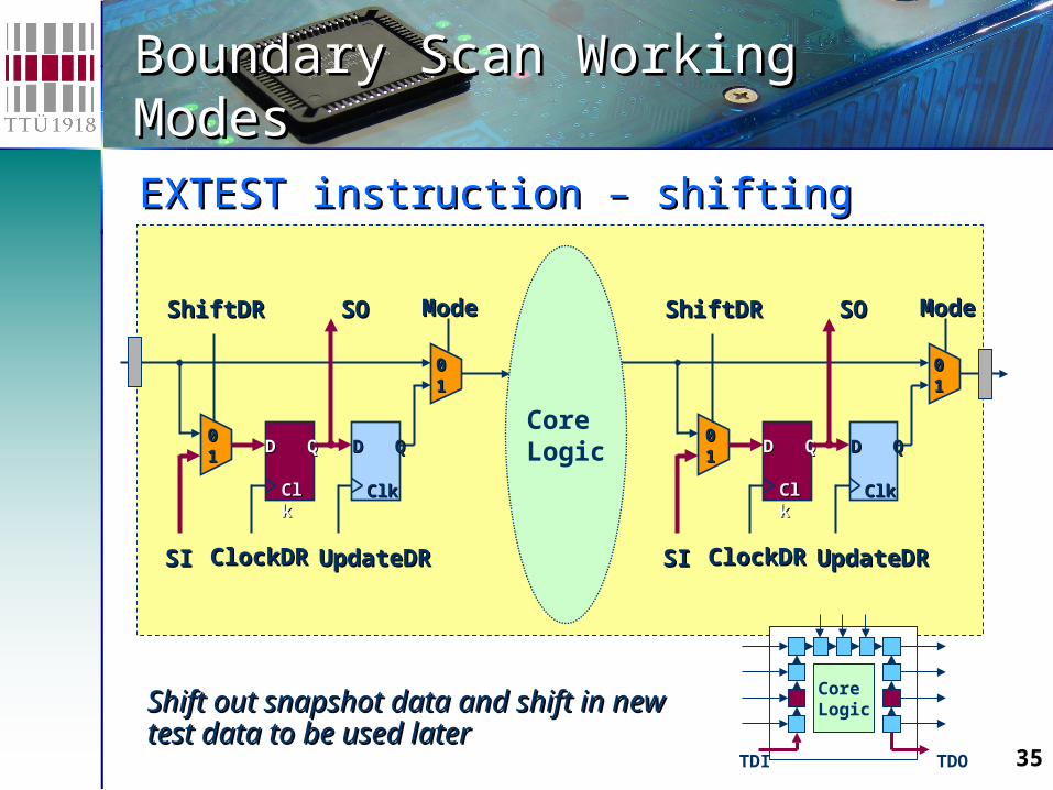
Boundary Scan Working ModesBoundary Scan Working Modes
EEXTESTXTEST instruction instruction – shifting– shifting
Shift out snapshot data and shift in new test data to be used Shift out snapshot data and shift in new test data to be used latlater
0011
D QD Q
ClkClk ClkClk
SOSO ModeModeShiftDRShiftDR
ClockDRClockDR UpdateDRUpdateDRSISI
0011
D QD Q0011
D QD Q
ClkClk ClkClk
SOSO ModeModeShiftDRShiftDR
ClockDRClockDR UpdateDRUpdateDRSISI
0011
D QD QCore Logic
Core Logic
TDOTDI
Shift out snapshot data and shift in Shift out snapshot data and shift in new test data to be used laternew test data to be used later
36
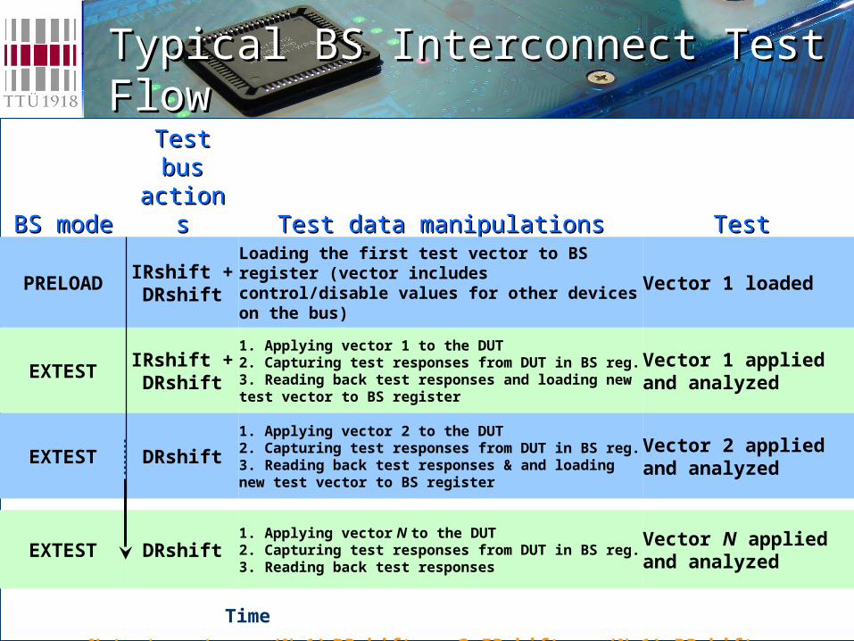
Typical BS Interconnect Test Typical BS Interconnect Test FlowFlow
BS modeBS mode
Test Test bus bus
actionsactions Test data manipulationsTest data manipulations Test Test
PRELOADIRshift + DRshift
Loading the first test vector to BS register (vector includes control/disable values for other devices on the bus)
Vector 1 loaded
EXTESTIRshift + DRshift
1. Applying vector 1 to the DUT2. Capturing test responses from DUT in BS reg.3. Reading back test responses and loading new test vector to BS register
Vector 1 applied and analyzed
EXTEST DRshift
1. Applying vector 2 to the DUT2. Capturing test responses from DUT in BS reg.3. Reading back test responses & and loading new test vector to BS register
Vector 2 applied and analyzed
EXTEST DRshift1. Applying vector N to the DUT2. Capturing test responses from DUT in BS reg.3. Reading back test responses
Vector N applied and analyzed
Time
N test vectors: (N+1) DRshifts + 2 IRshifts ≈ (N+1) DRshifts
37
Boundary Scan Working ModesBoundary Scan Working Modes
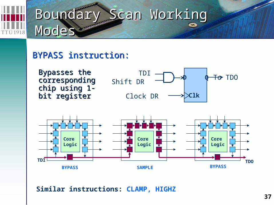
BBYPASSYPASS iinstructionnstruction::
To TDOTDI
Shift DR
Clock DR
D Q
Clk
Bypasses the Bypasses the corresponding corresponding chip using 1-chip using 1-bit registerbit register
Core Logic
TDO
Core Logic
TDI
Core Logic
BYPASS BYPASSSAMPLE
Similar instructions: CLAMP, HIGHZ
38
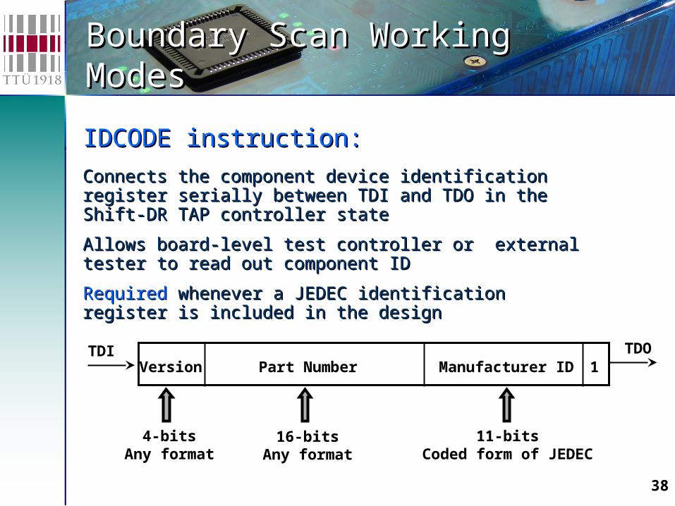
Boundary Scan Working ModesBoundary Scan Working Modes
IDCODE instructionIDCODE instruction::
Connects the component device identification register Connects the component device identification register serially between TDI and TDO in the Shift-DR TAP serially between TDI and TDO in the Shift-DR TAP controller statecontroller state
Allows board-level test controller or external tester to Allows board-level test controller or external tester to read out component IDread out component ID
RequiredRequired whenever a JEDEC identification register is whenever a JEDEC identification register is included in the designincluded in the design
TDOTDIVersion Part Number Manufacturer ID 1
4-bitsAny format
16-bitsAny format
11-bitsCoded form of JEDEC
39
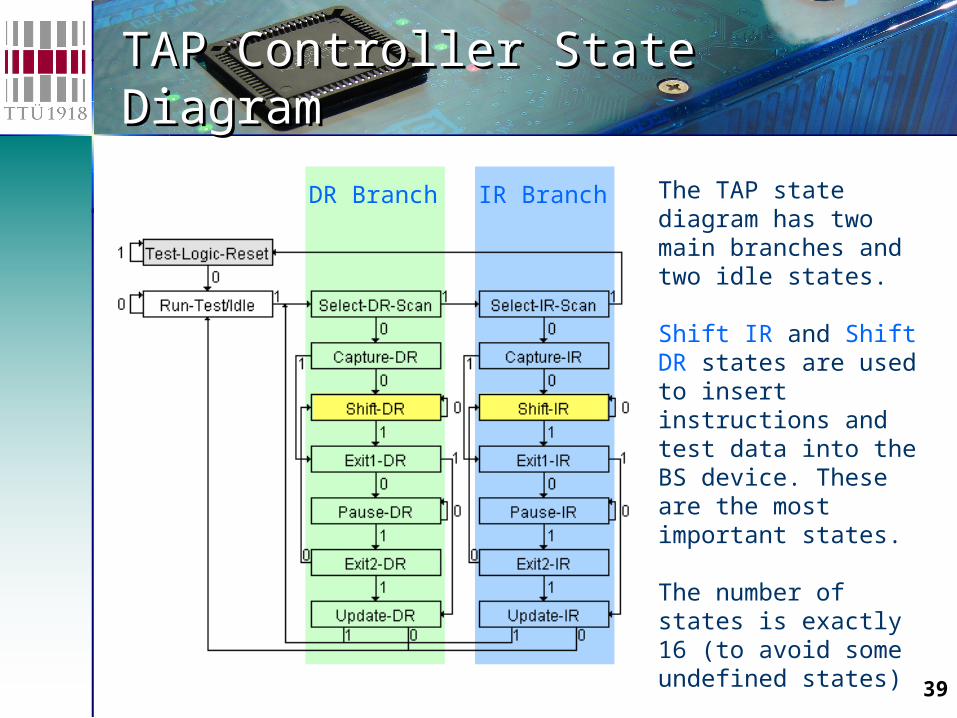
TAP Controller State DiagramTAP Controller State Diagram
IR BranchDR Branch The TAP state diagram has two main branches and two idle states.
Shift IR and Shift DR states are used to insert instructions and test data into the BS device. These are the most important states.
The number of states is exactly 16 (to avoid some undefined states)
TMS signal is used to move through the states
40
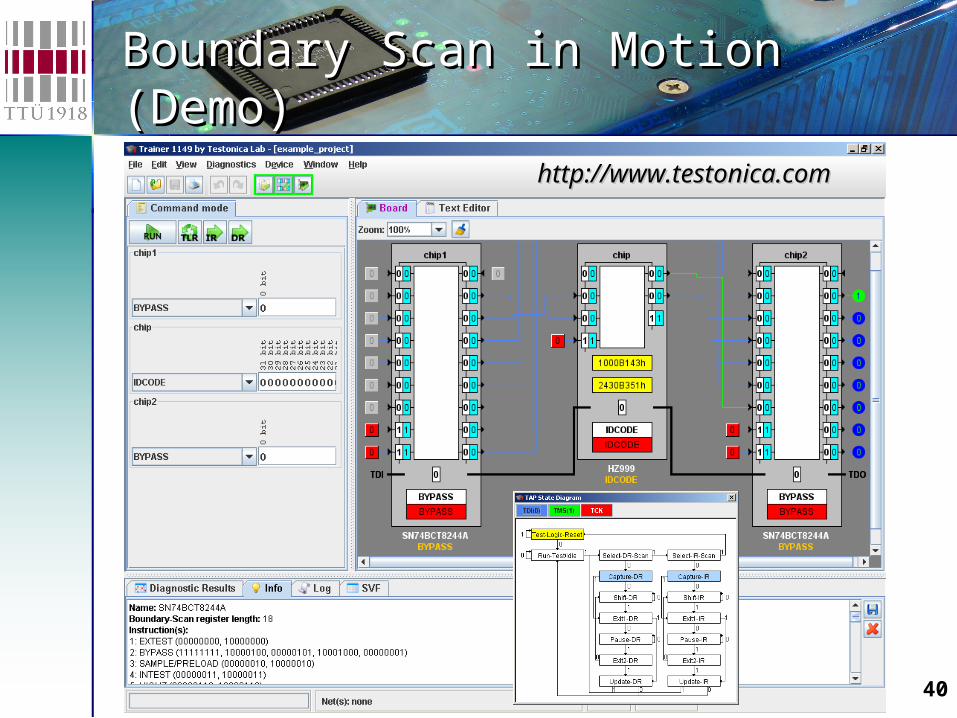
Boundary Scan in Motion Boundary Scan in Motion (Demo)(Demo)
http://www.testonica.comhttp://www.testonica.com
41
IEEE 1149.1 Boundary Scan IEEE 1149.1 Boundary Scan StandardStandard
• Board level testing challengesBoard level testing challenges
• Fault modeling at board level (digital)Fault modeling at board level (digital)
• IEEE 1149.1 Boundary Scan StandardIEEE 1149.1 Boundary Scan Standard
• Test generation for interconnect faultsTest generation for interconnect faults
• Application of Boundary ScanApplication of Boundary Scan
42
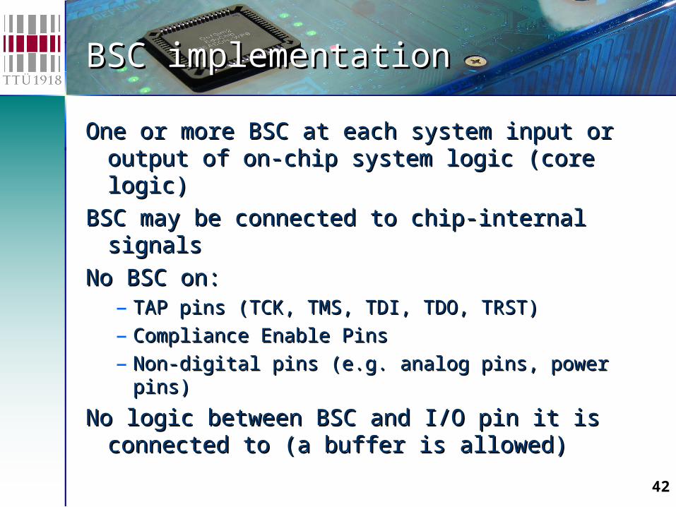
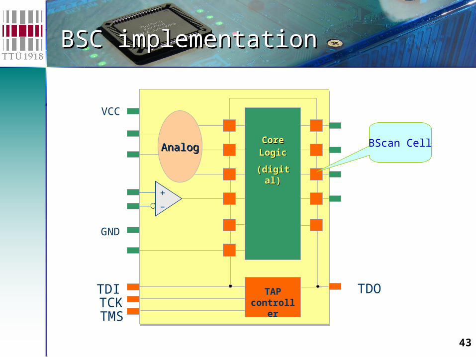
BSC implementationBSC implementation
One or more BSC at each system input or One or more BSC at each system input or output of on-chip system logic (core logic)output of on-chip system logic (core logic)
BSC may be connected to chip-internal BSC may be connected to chip-internal signalssignals
No BSC on:No BSC on:– TAP pins (TCK, TMS, TDI, TDO, TRST)TAP pins (TCK, TMS, TDI, TDO, TRST)
– Compliance Enable PinsCompliance Enable Pins
– Non-digital pins (e.g. analog pins, power pins)Non-digital pins (e.g. analog pins, power pins)
No logic between BSC and I/O pin it is No logic between BSC and I/O pin it is connected to (a buffer is allowed)connected to (a buffer is allowed)
43
BSC implementationBSC implementation
CoreCore LogicLogic
(digital)(digital)
TAPcontroller
BScan Cell
TDO
TMS
TDITCK
+–
VCC
GND
AnalogAnalog
44
BSC implementationBSC implementation
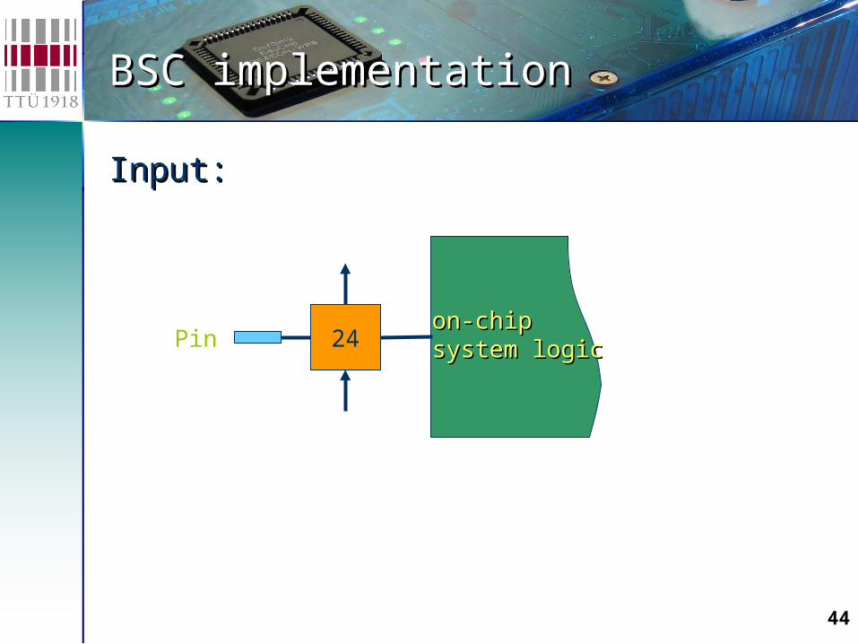
Input:Input:
24Pinon-chipon-chipsystem logicsystem logic
45
BSC implementationBSC implementation
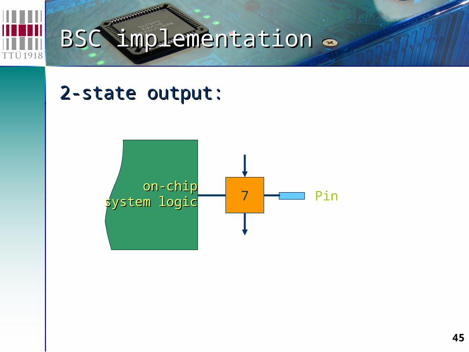
2-state output:2-state output:
7 Pinon-chipon-chip
system logicsystem logic
46
BSC implementationBSC implementation
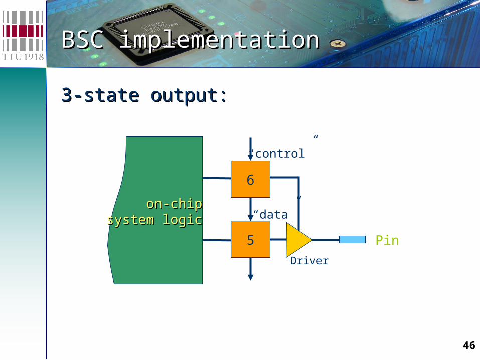
3-state output:3-state output:
Driver
“control”
“data”
5 Pin
on-chipon-chipsystem logicsystem logic
6
47
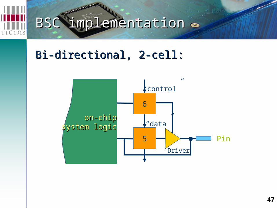
Driver
“control”
“data”
5 Pin
on-chipon-chipsystem logicsystem logic
6
BSC implementationBSC implementation
Bi-directional, 2-cell:Bi-directional, 2-cell:
48
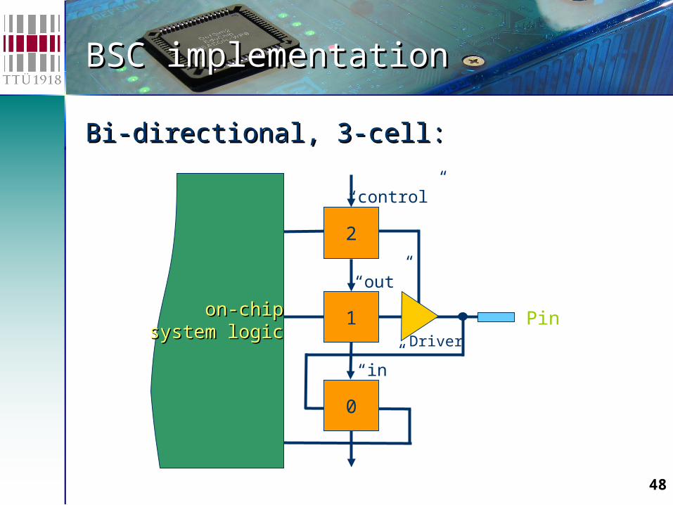
BSC implementationBSC implementation
Bi-directional, 3-cell:Bi-directional, 3-cell:
Driver
“control”
“out”
1 Pinon-chipon-chipsystem logicsystem logic
2
0
“in”
49
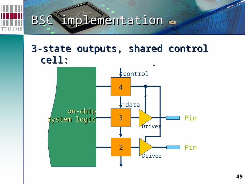
BSC implementationBSC implementation
3-state outputs, shared control cell:3-state outputs, shared control cell:
Driver
“control”
“data”
3 Pin
4
Driver
2 Pin
on-chipon-chipsystem logicsystem logic
50
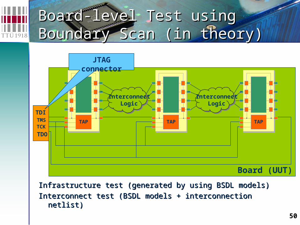
Board-level Test using Board-level Test using Boundary Scan (in theory)Boundary Scan (in theory)
Board (UUT)
TDITMSTCK
TAP TAP TAP
InterconnectLogic
InterconnectLogic
TDO
JTAG connector
Infrastructure test (generated by using BSDL models)Infrastructure test (generated by using BSDL models)
Interconnect test (BSDL models + interconnection Interconnect test (BSDL models + interconnection netlist)netlist)
51
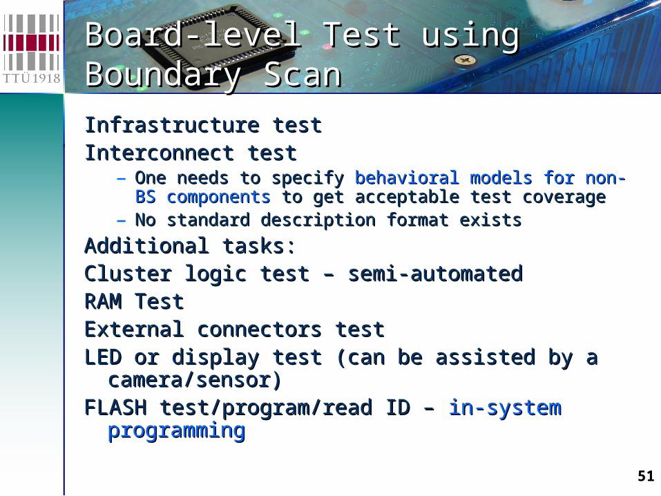
Board-level Test using Board-level Test using Boundary ScanBoundary Scan
Infrastructure testInfrastructure testInterconnect testInterconnect test
– One needs to specify One needs to specify behavioral models for non-BS behavioral models for non-BS componentscomponents to get acceptable test coverage to get acceptable test coverage
– No standard description format existsNo standard description format exists
Additional tasks:Additional tasks:Cluster logic test – semi-automatedCluster logic test – semi-automatedRAM TestRAM TestExternal connectors testExternal connectors testLED or display test (can be assisted by a LED or display test (can be assisted by a
camera/sensor)camera/sensor)FLASH test/program/read ID – FLASH test/program/read ID – in-system in-system
programmingprogramming
52
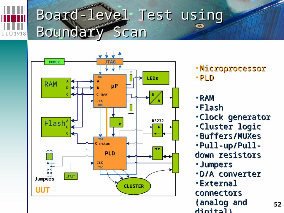
Board-level Test using Board-level Test using Boundary ScanBoundary Scan
PLD
TDI
TDO
TDI
TDO
µP
UUT
JTAG
RAMA
D
C
Flash A
D
C
C (FLASH)
A
D
C (RAM)
CLK
LEDs
Jumpers
CLUSTER
RS232
D
ACLK
POWER
•MicroprocessorMicroprocessor•PLDPLD
•RAMRAM•FlashFlash•Clock generatorClock generator•Cluster logicCluster logic•Buffers/MUXesBuffers/MUXes•Pull-up/Pull-down Pull-up/Pull-down resistorsresistors•JumpersJumpers•D/A converterD/A converter•External connectorsExternal connectors(analog and digital)(analog and digital)
53
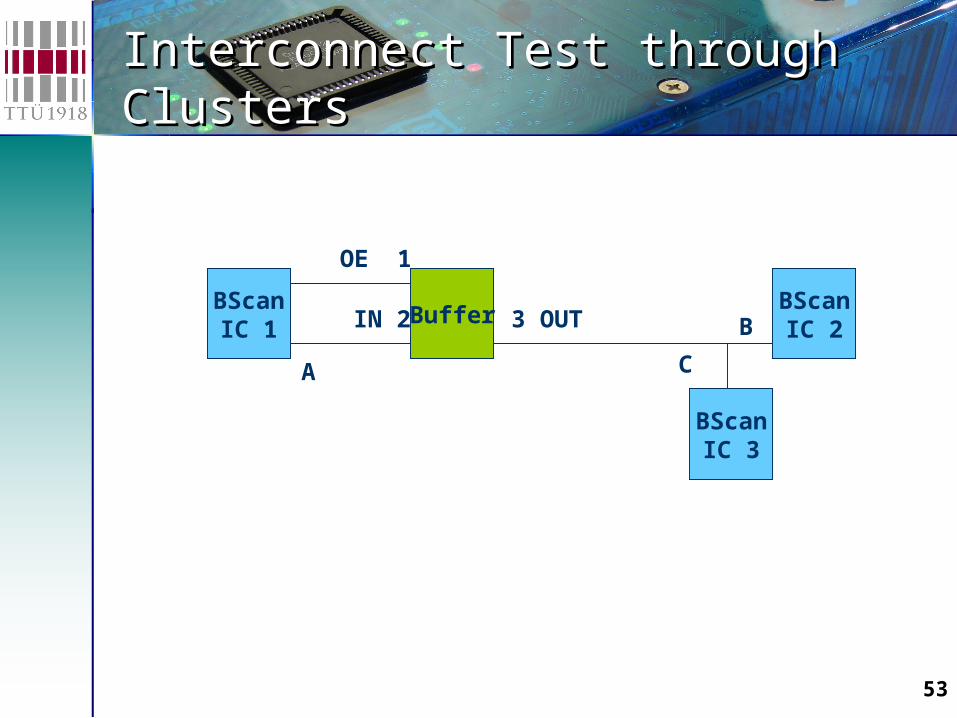
Interconnect Test through Interconnect Test through ClustersClusters
BScanIC 1
BScanIC 2
Buffer
BScanIC 3
OE 1
IN 2 3 OUT
A
B
C
54
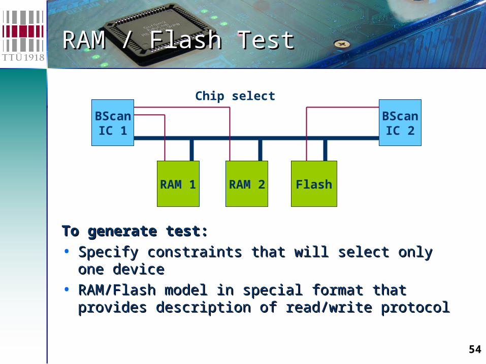
RAM / Flash TestRAM / Flash Test
BScanIC 1
BScanIC 2
RAM 2 FlashRAM 1
Chip select
To generate test:To generate test:
• Specify constraints that will select only one Specify constraints that will select only one devicedevice
• RAM/Flash model in special format that RAM/Flash model in special format that provides description of read/write protocolprovides description of read/write protocol
55
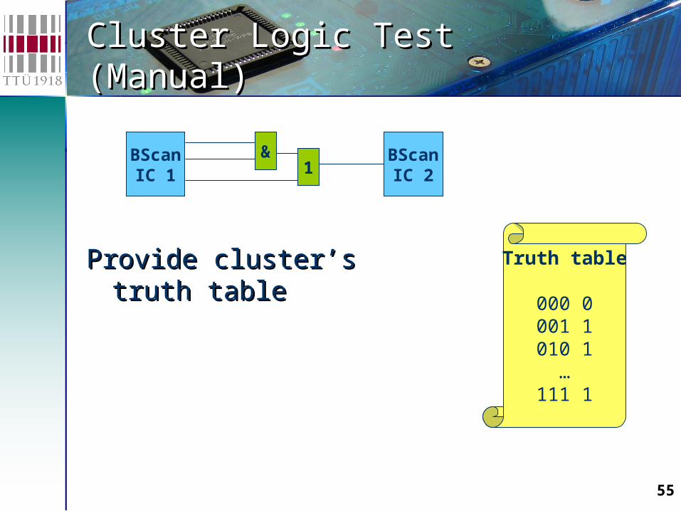
Cluster Logic Test (Manual)Cluster Logic Test (Manual)
Provide cluster’s truth Provide cluster’s truth tabletable
BScanIC 1
BScanIC 2
&1
Truth table
000 0001 1010 1
…111 1
56
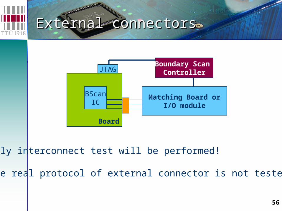
External connectorsExternal connectors
Board
JTAG
BScanIC
Matching Board orI/O module
Boundary Scan Controller
Only interconnect test will be performed!
The real protocol of external connector is not tested
57
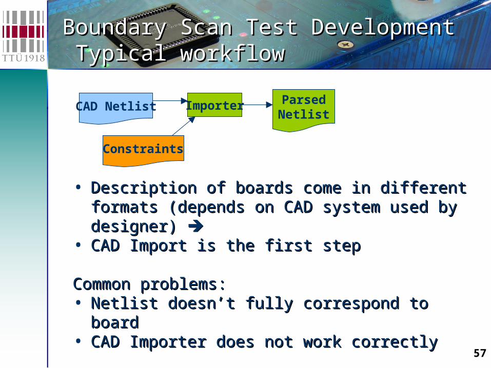
Boundary Scan Test Development Boundary Scan Test Development Typical workflowTypical workflow
CAD Netlist Importer ParsedNetlist
• Description of boards come in different Description of boards come in different formats (depends on CAD system used by formats (depends on CAD system used by designer) designer)
• CAD Import is the first stepCAD Import is the first step
Common problems:Common problems:• Netlist doesn’t fully correspond to boardNetlist doesn’t fully correspond to board• CAD Importer does not work correctlyCAD Importer does not work correctly
Constraints
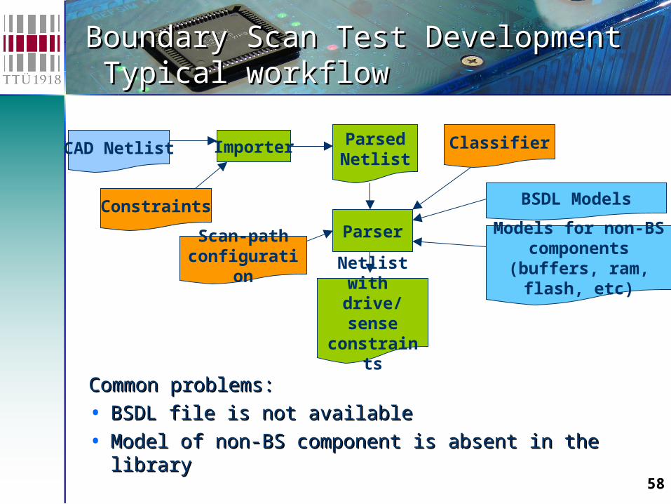
58
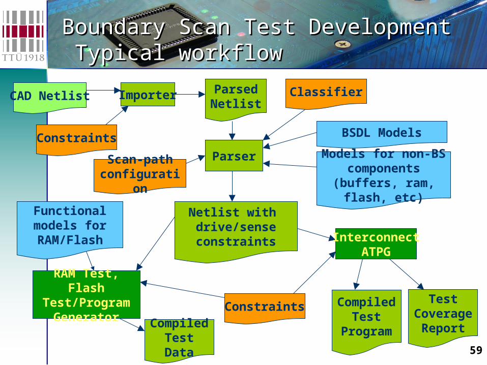
Boundary Scan Test Development Boundary Scan Test Development Typical workflowTypical workflow
CAD Netlist
Constraints
Importer ParsedNetlist
Classifier
Parser
BSDL Models
Scan-path configuration
Netlist with drive/sense constraints
Models for non-BS components (buffers,
ram, flash, etc)
Common problems:Common problems:
• BSDL file is not availableBSDL file is not available
• Model of non-BS component is absent in the libraryModel of non-BS component is absent in the library
59
Boundary Scan Test Development Boundary Scan Test Development Typical workflowTypical workflow
CAD Netlist
Constraints
Importer ParsedNetlist
Classifier
Parser
BSDL Models
Scan-path configuration
Netlist with drive/sense constraints Interconnect
ATPG
Test Coverage
Report
Compiled Test
Program
RAM Test, Flash Test/Program
Generator
Compiled Test Data
Functional models for RAM/Flash
Models for non-BS components (buffers,
ram, flash, etc)
Constraints
60
IEEE 1149.1 SummaryIEEE 1149.1 Summary
Boundary Scan Standard has become Boundary Scan Standard has become absolutely essential:absolutely essential:
− No longer possible to test printed circuit No longer possible to test printed circuit boards with bed-of-nails tester boards with bed-of-nails tester
− Not possible to test multi-chip modules Not possible to test multi-chip modules at all without itat all without it
− Supports BIST, external testing with Supports BIST, external testing with Automatic Test Equipment, and Automatic Test Equipment, and boundary scan chain reconfiguration as boundary scan chain reconfiguration as BIST pattern generator and response BIST pattern generator and response compactercompacter
− Now getting widespread usageNow getting widespread usage
61
Boundary Scan – EvolutionBoundary Scan – Evolution
1149.4 – 1149.4 – Mixed-Signal Test BusMixed-Signal Test Bus (testing analog signals) (testing analog signals)
1149.6 – Boundary-Scan Testing of Advanced Digital 1149.6 – Boundary-Scan Testing of Advanced Digital Networks (testing high speed links)Networks (testing high speed links)
1149.7 – CJTAG – Compact JTAG (debug)1149.7 – CJTAG – Compact JTAG (debug)
1149.8.1 – Sensing using capacitive plate1149.8.1 – Sensing using capacitive plate
P1687 – IJTAG – Internal JTAG (component testing, BIST)P1687 – IJTAG – Internal JTAG (component testing, BIST)
1500 – Embedded Core Test (SoC testing)1500 – Embedded Core Test (SoC testing)
1532 – In-System Configuration of Programmable Devices1532 – In-System Configuration of Programmable Devices
P1581 – Static Component Interconnection Test Protocol P1581 – Static Component Interconnection Test Protocol and Architecture (memory-to-BS_chip links testing)and Architecture (memory-to-BS_chip links testing)
5001 – NEXUS – Global Embedded Processor Debug 5001 – NEXUS – Global Embedded Processor Debug Interface (SW development, debug, and emulation)Interface (SW development, debug, and emulation)
62
What to look furtherWhat to look further
Leading BScan companies:Leading BScan companies:– Goepel Electronic (http://www.goepel.com/)Goepel Electronic (http://www.goepel.com/)– ASSET Intertech (http://www.asset-intertech.com/)ASSET Intertech (http://www.asset-intertech.com/)– JTAG Technologies (http://www.jtag.com/)JTAG Technologies (http://www.jtag.com/)
Training software:Training software:– Trainer 1149 by Testonica Lab Trainer 1149 by Testonica Lab
(http://www.testonica.com/1149/download.htm)(http://www.testonica.com/1149/download.htm)– Scan Coach by Goepel Electronic Scan Coach by Goepel Electronic
(http://www.goepel.com/content/html_en/index.php?(http://www.goepel.com/content/html_en/index.php?site=bs_BScanCoach)site=bs_BScanCoach)
– Scan Educator by Texas Instruments Scan Educator by Texas Instruments (http://focus.ti.com/docs/toolsw/folders/print/scan_educator.html)(http://focus.ti.com/docs/toolsw/folders/print/scan_educator.html)
Literature:Literature:– Kenneth P. ParkerKenneth P. Parker, , The Boundary-Scan HandbookThe Boundary-Scan Handbook– Lecture notes by Ben BennettsLecture notes by Ben Bennetts
Active Universities:Active Universities:– Porto, PortugalPorto, Portugal– Tallinn, EstoniaTallinn, Estonia– Liberec and Prague, Czech RepublicLiberec and Prague, Czech Republic– Lubljana, SloveniaLubljana, Slovenia