
Blackening of metals using femtosecond fiber laser · Blackening of metals using femtosecond fiber...
10
Blackening of metals using femtosecond fiber laser Huan Huang,* Lih-Mei Yang, Shuang Bai, and Jian Liu PolarOnyx, Inc. 2526 Qume Drive, Suite 17 & 18, San Jose, California 94538, USA *Corresponding author: [email protected] Received 2 October 2014; revised 25 November 2014; accepted 28 November 2014; posted 1 December 2014 (Doc. ID 224015); published 9 January 2015 This study presents an unprecedented high throughput processing for super-blackening and superhydro- phobic/hydrophilic surface on both planar and nonplanar metals surfaces. By using a high pulse repeti- tion rate femtosecond (fs) fiber laser, a light trapping microstructure and nanostructure is generated to absorb light from UV, visible to long-wave infrared spectral region. Different types of surface structures are produced with varying laser scanning conditions (scanning speed and pitch). The modified surface morphologies are characterized using scanning electron microscope and the blackening effect is inves- tigated through spectral measurements. Spectral measurements show that the reflectance of the proc- essed materials decreases sharply in a wide wavelength range and the decrease occurs at different rates for different scanning pitches and speeds. Above 98% absorption over the entire visible wavelength region and above 95% absorption over the near-infrared, middle-wave infrared and long-wave infrared regions range has been demonstrated for the surface structures, and the absorption for specific wavelengths can go above 99%. Furthermore, the processing efficiency of this fs fiber laser blackening technique is 1 order of magnitude higher than that of solid-state fs laser and 4 times higher than that of picosecond (ps) laser. Further increasing of the throughput is expected by using higher repetition and higher scanning speed. This technology offers the great potential in applications such as constructing sensitive detectors and sensors, solar energy absorber, and biomedicine. © 2015 Optical Society of America OCIS codes: (060.3510) Lasers, fiber; (140.3390) Laser materials processing; (220.4000) Microstruc- ture fabrication; (220.4241) Nanostructure fabrication. http://dx.doi.org/10.1364/AO.54.000324 1. Introduction Recently, femtosecond (fs) laser direct writing has become an advanced tool for high-quality material microprocessing and nanoprocessing, more control- lable with minimal thermal damage to surrounding materials. Among these, laser surface modification has been increasingly investigated to synthetically alter surface properties, such as optical properties [ 1– 10], wettability [ 11– 15], and biological properties [ 16– 19]. Blackening and coloring of metal and non- metal surfaces are important to both military and commercial applications, such as camouflage, optical sensing and imaging, countermeasure, solar cell, engraving, marking, etc. Researchers have already made advances in this fs laser blackening field by using solid-state Ti:sappire fs lasers. For example, Mazur and co-workers [ 1, 2] conducted the pioneering work of fs laser-induced microstructuring on silicon surface and improved its optoelectron conversion efficiency. Vorobyev and Guo [ 4, 6] developed a technique to transform highly reflective metals to be either totally absorptive or re- flecting only a certain color of light, creating so-called black or colored metals by using fs laser direct writing. However, the blackening by using solid-state fs laser is quite time consuming, the processing speed is usu- ally in the magnitude of micrometers per second. The speed is mainly limited by the low pulse repetition rate (kHz) of Ti:sappire fs lasers. Moreover, solid-state fs lasers are bulky, expensive,and not user friendly. Researchers have tried to increase the processing speed by using different methods, such as the 1559-128X/15/020324-10$15.00/0 © 2015 Optical Society of America 324 APPLIED OPTICS / Vol. 54, No. 2 / 10 January 2015
Transcript of Blackening of metals using femtosecond fiber laser · Blackening of metals using femtosecond fiber...
Blackening of metals using femtosecond fiber laser
Huan Huang,* Lih-Mei Yang, Shuang Bai, and Jian LiuPolarOnyx, Inc. 2526 Qume Drive, Suite 17 & 18, San Jose, California 94538, USA
*Corresponding author: [email protected]
Received 2 October 2014; revised 25 November 2014; accepted 28 November 2014;posted 1 December 2014 (Doc. ID 224015); published 9 January 2015
This study presents an unprecedented high throughput processing for super-blackening and superhydro-phobic/hydrophilic surface on both planar and nonplanar metals surfaces. By using a high pulse repeti-tion rate femtosecond (fs) fiber laser, a light trapping microstructure and nanostructure is generated toabsorb light from UV, visible to long-wave infrared spectral region. Different types of surface structuresare produced with varying laser scanning conditions (scanning speed and pitch). The modified surfacemorphologies are characterized using scanning electron microscope and the blackening effect is inves-tigated through spectral measurements. Spectral measurements show that the reflectance of the proc-essed materials decreases sharply in a wide wavelength range and the decrease occurs at different ratesfor different scanning pitches and speeds. Above 98% absorption over the entire visible wavelength regionand above 95% absorption over the near-infrared, middle-wave infrared and long-wave infrared regionsrange has been demonstrated for the surface structures, and the absorption for specific wavelengths cango above 99%. Furthermore, the processing efficiency of this fs fiber laser blackening technique is 1 orderof magnitude higher than that of solid-state fs laser and 4 times higher than that of picosecond (ps) laser.Further increasing of the throughput is expected by using higher repetition and higher scanning speed.This technology offers the great potential in applications such as constructing sensitive detectors andsensors, solar energy absorber, and biomedicine. © 2015 Optical Society of AmericaOCIS codes: (060.3510) Lasers, fiber; (140.3390) Laser materials processing; (220.4000) Microstruc-
ture fabrication; (220.4241) Nanostructure fabrication.http://dx.doi.org/10.1364/AO.54.000324
1. Introduction
Recently, femtosecond (fs) laser direct writing hasbecome an advanced tool for high-quality materialmicroprocessing and nanoprocessing, more control-lable with minimal thermal damage to surroundingmaterials. Among these, laser surface modificationhas been increasingly investigated to syntheticallyalter surface properties, such as optical properties[1–10], wettability [11–15], and biological properties[16–19]. Blackening and coloring of metal and non-metal surfaces are important to both military andcommercial applications, such as camouflage, opticalsensing and imaging, countermeasure, solar cell,engraving, marking, etc.
Researchers have already made advances in this fslaser blackening field by using solid-state Ti:sappirefs lasers. For example, Mazur and co-workers [1,2]conducted the pioneering work of fs laser-inducedmicrostructuring on silicon surface and improvedits optoelectron conversion efficiency. Vorobyev andGuo [4,6] developed a technique to transform highlyreflective metals to be either totally absorptive or re-flecting only a certain color of light, creating so-calledblack or coloredmetals byusing fs laser directwriting.However, the blackening by using solid-state fs laseris quite time consuming, the processing speed is usu-ally in the magnitude of micrometers per second. Thespeed is mainly limited by the low pulse repetitionrate (kHz) ofTi:sappire fs lasers.Moreover, solid-statefs lasers are bulky, expensive, and not user friendly.
Researchers have tried to increase the processingspeed by using different methods, such as the
1559-128X/15/020324-10$15.00/0© 2015 Optical Society of America
324 APPLIED OPTICS / Vol. 54, No. 2 / 10 January 2015
interferometric method [20,21] or a nanosecond (ns)laser [22], but the high throughput was compromisedby reduced blackness. Furthermore, the ns lasercould cause heat buildup, resulting in product distor-tion and progressive variation in color. Recently,higher processing throughput was obtained by usinga picosecond (ps) laser for copper blackening [23], butit is still not enough for industrial applications.Recent advances in laser technology have evolvedmore compact and reliable high-power and highrepetition rate fs fiber lasers for many industrialapplications.
In this paper, super-blackening of metals using ahigh-power and high repetition rate fs fiber laseris studied. The fs laser blackening mechanisms arediscussed. Different laser writing conditions, includ-ing pulse energy, repetition rate, writing speed, andpitch, are investigated for the blackening effect.Different surface morphologies are generated andcharacterized using optical microscopy and scanningelectron microscopy (SEM). The wavelength depend-ence of the reflectance of electromagnetic irradia-tions in the UV, visible, near-infrared (NIR),middle-wave infrared (MWIR), and long-wave infra-red (LWIR) regions is characterized and measured.For specific wavelength the reflectance can be lessthan 1%. In addition to the high broadband absorp-tion, this process can also make the surfaces hydro-phobic or hydrophilic simultaneously. Furthermore,the fs fiber laser based method enables the process-ing speed up to hundreds of millimeters per second,much higher than those reported with other lasers.This novelty makes the high-power and high repeti-tion rate fs fiber laser an efficient and affordablemethod for practical industrial applications.
2. Experimental Setup and Materials
For the experimental setup, it comprises a mode-locked fiber laser system, beam delivery components,an acousto-optic modulator (AOM), an automatedmotion system, a sample fixture, and a computerfor system control. The fs fiber laser system was acommercialized high-energy fiber laser (UranusSeries, PolarOnyx Laser, Inc.), generating 750 fspulses (FWHM) at 1030 nm wavelength with pulserepetition rate from 50 kHz up to 1 MHz. In theexperiments, the laser beam was guided by mirrorstoward to a scanner (ScanCube 10, SCANLAB AG)and focused by an F-theta lens (f � 100 mm) ontothe sample. The sample was mounted on a computer-controlled five-dimensional translation stage. Thepulse energy was adjustable by the AOM. The outputcollimated beam was a nearly symmetric Gaussianwith M2 < 1.3 and the maximum output pulse en-ergy was 500 μJ. An attenuator was used to controlthe laser pulse energy. The total beam delivery losswas less than 20%. A CCD camera was used to obtaina live view for the laser direct writing. All experi-ments were carried out in ambient air. Before andafter the laser processing, the samples were cleanedby an ultrasonic cleaner. The focal spot size for the
laser beam was 25 μm (1∕e2). A constant air flowwas placed across the sample surface during theexperiment to flush out the plume of ablated andrecondensed material.
In this study, different types ofmetalswere used forlaser directwriting, including aluminum, copper, tita-nium, and stainless steel. Samples were prepolishedand carefully cleaned before each experiment. Afterthe laser processing and polishing, the laser writtenstructures were captured and characterized byoptical transmission microscopy (ME520T-9M). Thena SEM (FEI QUANTA FEG 600) with energy-dispersivex-rayspectroscopy(EDS)detectorwasusedto further characterize and measure the features.
The wavelength dependence of the total reflec-tance was characterized with different spectropho-tometers for different wavelength ranges. Thereflectance for visible wavelength (360–740 nm)was measured by using a visible wavelength spectro-photometer (CM-2600d, Konica Minolta), and it pro-vides both L � a � b values (CIELab color space) andtotal reflectance values. To explore the reflectance inthe NIR, MWIR and LWIR region, a NIR spectropho-tometer (200 nm–2.5 μm, LAMBDA 1050 UV/Vis/NIR, Perkin Elmer) and a FT-IR spectrometer(2.5–15 μm, Frontier FT-NIR/MIR, Perkin Elmer)were used. For the total reflectance measurement,an integrating sphere with 150 mm diameter wasused to measure both the specular and diffuse reflec-tions of the processed surface.
3. Experimental Results and Discussion
To systematically study the blackening effect usingan fs fiber laser, different laser parameters andprocessing conditions were evaluated for differentmetals. A series of experiments were carried out toinvestigate the correlation of blackening quality withlaser pulse energy, repetition rate, pitch, and scan-ning speed.
A. Mechanism and Process Optimization
1. Aluminum BlackeningAluminum blackening was conducted with variousconditions, including scanning speed (0.001–1 m∕s),pulse energy (2.8–13.5 μJ), and scanning pitch(5–50 μm). The pulse repetition rate was fixed at100 kHz. For each parameter set, the sample wasscanned in both horizontal and vertical directions.The scanning pitch (5–50 μm) covers from smallerto larger than focal spot size.
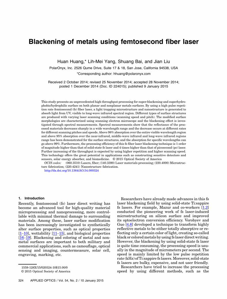
Several kinds of surface colors (Fig. 1) can be gen-erated on the aluminum surfaces by varying the
Fig. 1. Photographs of modified aluminum surface showing dif-ferent colors: (a) gray; (b) golden; (c) black; and (d) white.
10 January 2015 / Vol. 54, No. 2 / APPLIED OPTICS 325
scanning conditions. It is believed that the surfacecolors of the modified area are mainly related tothe surface morphology [3–6,22,23]. Given the samepulse energy and pitch, as the scanning speed de-creases from 500 to 2 mm∕s, the color goes from lightgray, gold, black, to white. For the same pulse energyand scanning speed, the color becomes darker withthe decreasing scanning pitch.
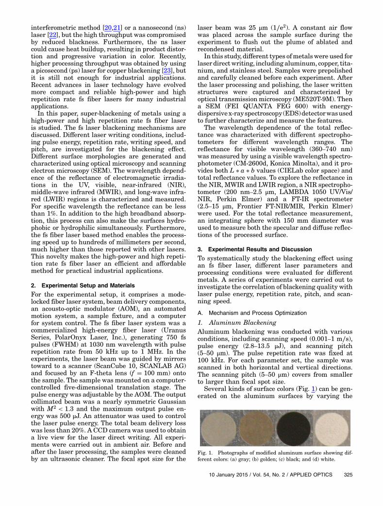
Figure 2(a) shows themeasured total reflectance ofthe aluminum sample as a function of wavelength fordifferent scanning pitches. The fs fiber laser process-ing with proper parameters significantly decreasesthe reflectance of the aluminum surfaces in a broad-band spectrum. Strong light absorption was achievedafter processing on initially high-reflective polishedaluminum surfaces. The scanning pitch betweentwo adjacent lines has obvious influence on the reflec-tancewhen using the same pulse energy (13.5 μJ) andscanning speed (10 mm∕s). As the scanning pitchincreases from 5 to 50 μm, the total reflectanceincreases. For each scanning pitch, the reflectance in-creases with the wavelength. The lowest reflectancewas obtained with a scanning interval of 5 μm, withover 95% absorptivity in the visible spectral regionand 97% absorptivity at some specific wavelength(s).
Figure 2(b) shows the reflectance as a function ofwavelength with different scanning speeds. Otherscanning conditions are kept the same—13.5 μJpulse energy and 10 μm scanning pitch. At low scan-ning speeds (e.g., 50 mm∕s), the reflectance for thewhole wavelength range is almost uniform and thetotal reflectance is less than 2%. At 100 mm∕s scan-ning speed, the reflectance increases with the wave-length but the total reflectance is still less than 5%.At even higher scanning speeds (200 and 300 mm∕s),the wavelength-dependent reflectance increasesmore dramatically and the total reflectance is about6% and 9%, respectively. It is worth to mention thatwith further decreases of the scanning speed to 5 or2 mm∕s, the reflectance suddenly increases and thealuminum surface becomes white rather than blackcolor (Fig. 1).
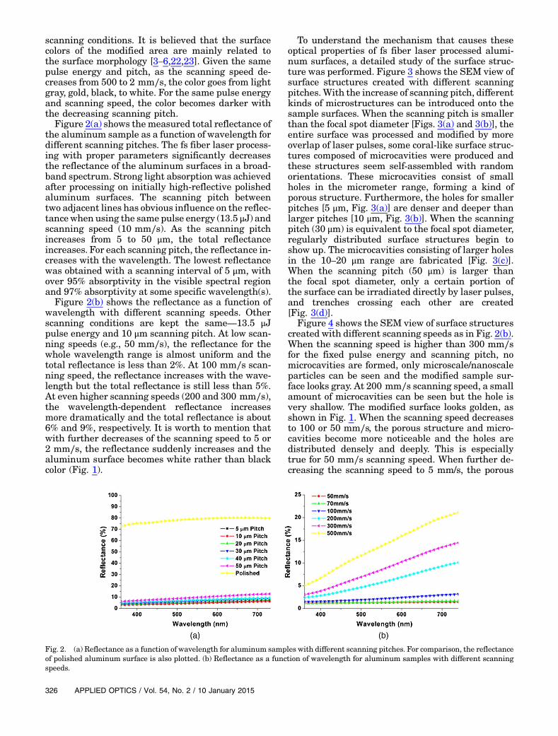
To understand the mechanism that causes theseoptical properties of fs fiber laser processed alumi-num surfaces, a detailed study of the surface struc-ture was performed. Figure 3 shows the SEM view ofsurface structures created with different scanningpitches. With the increase of scanning pitch, differentkinds of microstructures can be introduced onto thesample surfaces. When the scanning pitch is smallerthan the focal spot diameter [Figs. 3(a) and 3(b)], theentire surface was processed and modified by moreoverlap of laser pulses, some coral-like surface struc-tures composed of microcavities were produced andthese structures seem self-assembled with randomorientations. These microcavities consist of smallholes in the micrometer range, forming a kind ofporous structure. Furthermore, the holes for smallerpitches [5 μm, Fig. 3(a)] are denser and deeper thanlarger pitches [10 μm, Fig. 3(b)]. When the scanningpitch (30 μm) is equivalent to the focal spot diameter,regularly distributed surface structures begin toshow up. The microcavities consisting of larger holesin the 10–20 μm range are fabricated [Fig. 3(c)].When the scanning pitch (50 μm) is larger thanthe focal spot diameter, only a certain portion ofthe surface can be irradiated directly by laser pulses,and trenches crossing each other are created[Fig. 3(d)].
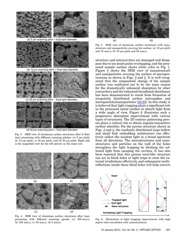
Figure 4 shows the SEM view of surface structurescreated with different scanning speeds as in Fig. 2(b).When the scanning speed is higher than 300 mm∕sfor the fixed pulse energy and scanning pitch, nomicrocavities are formed, only microscale/nanoscaleparticles can be seen and the modified sample sur-face looks gray. At 200 mm∕s scanning speed, a smallamount of microcavities can be seen but the hole isvery shallow. The modified surface looks golden, asshown in Fig. 1. When the scanning speed decreasesto 100 or 50 mm∕s, the porous structure and micro-cavities become more noticeable and the holes aredistributed densely and deeply. This is especiallytrue for 50 mm∕s scanning speed. When further de-creasing the scanning speed to 5 mm/s, the porous
Fig. 2. (a) Reflectance as a function of wavelength for aluminum samples with different scanning pitches. For comparison, the reflectanceof polished aluminum surface is also plotted. (b) Reflectance as a function of wavelength for aluminum samples with different scanningspeeds.
326 APPLIED OPTICS / Vol. 54, No. 2 / 10 January 2015
structure and microcavities are damaged and disap-pear due to toomuch pulse overlapping, and the proc-essed sample surface shows white color in Fig. 1.Figure 5 shows the SEM view of nanostructureand nanoparticles covering the surface of micropro-trusions as shown in Figs. 3 and 4. It is well recog-nized that the composition change of the samplesurface was confirmed not to be the main reasonfor the dramatically enhanced absorption by otherresearchers and the enhanced broadband absorbancehas been demonstrated to result from formation ofirregularly distributed surface microspikes andmicroparticles/nanoparticles [22,23]. In this study, itis believed that light trapping plays a significant rolein the processed metal surface to absorb light froma wide angle of view. Figure 6 illustrates such aprogressive absorption improvement with varioustypes of structures. The 2D contour patterning proc-ess plays a critical role to obtain angular-insensitivesurface absorber. For the porous structure shown inFigs. 3 and 4, the randomly distributed large hollowand small hole embedding architecture can effec-tively collect the incident light in a broad spectrumfrom all directions. The microstructures and nano-structures and particles on the wall of the holesstrengthen the light trapping by blocking the col-lected light from escaping the cavities. It has alsobeen reported that this porous coral-like structurecan act as black holes or light traps to seize the ex-ternal irradiations effectively, and subsequent multi-reflections inside these blind holes will help convert
(d) 50 µm scanning pitch > focal spot diameter
(b) 10 µm scanning pitch < focal spot diameter
(a) 5 µm scanning pitch < focal spot diameter
(c) 30 µm scanning pitch ∼ focal spot diameter
Fig. 3. SEM view of aluminum surface structures after fs fiberlaser processing with different scanning pitches: (a) 5 μm pitch;(b) 10 μm pitch; (c) 30 μm pitch; and (d) 50 μm pitch. Right sideis the magnified view for the left picture on the same row.
(a) (b)
(c) (d)
Fig. 4. SEM view of aluminum surface structures after laserprocessing with different scanning speeds: (a) 300 mm∕s,(b) 100 mm∕s, (c) 50 mm∕s, (d) 5 mm∕s.
(a) (b)
Fig. 5. SEM view of aluminum surface structures with nano-structure and nanoparticles covering the surface: (a) 10 μm pitchand 10 mm∕s; (b) 10 μm pitch and 50 mm∕s.
Input
Trapped lightExit light
Increasing Light Trapping
Nano structure
Fig. 6. Illustration of light trapping improvement with highaspect ratio microholes with nanostructures.
10 January 2015 / Vol. 54, No. 2 / APPLIED OPTICS 327
the light energy into the heat through iterativeabsorption [5].
The blackening effect shows a strong relationshipwith the spatial overlapping of laser pulses. Asshown in Fig. 2, good results were obtained whensmaller scanning pitch (e.g., 5–10 μm) or slower scan-ning speed (e.g., 10–50 mm∕s) was used. Duringpulse laser treatment, two factors influence theblackening results, namely pulse energy and pulseoverlap rate (total pulse numbers for one spot).The pulse overlap rate is defined by scanning speed,scanning pitch, and pulse repetition rate. At the fixedrepetition rate, a smaller pitch or slower speed cre-ates more pulse overlapping and accordingly morelaser energy irradiated at one spot. So it was antici-pated that 250–1250 pulses per spot was a properrange for the enhancement of absorptance underthe highest pulse energy utilized in this study;higher pulse overlapping on the sample surface willdamage the surface structure created by previouspulses and a white color surface would be obtained.
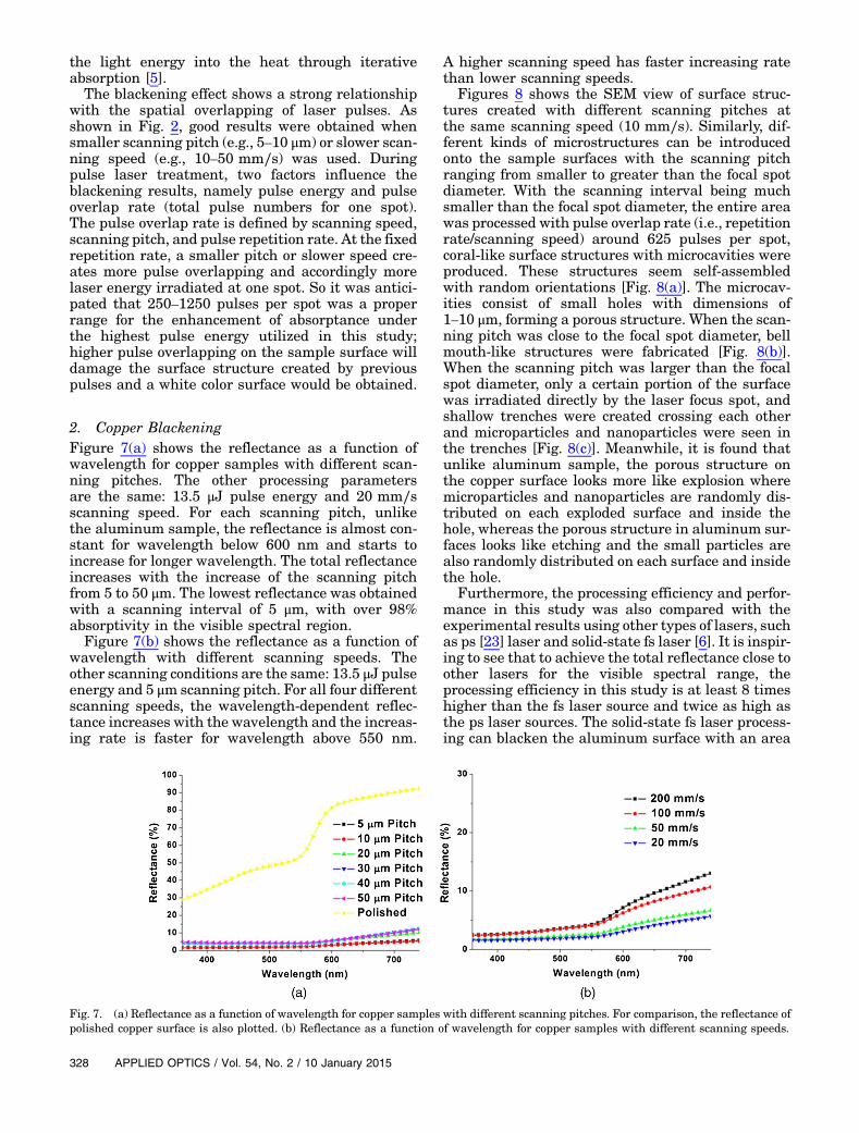
2. Copper BlackeningFigure 7(a) shows the reflectance as a function ofwavelength for copper samples with different scan-ning pitches. The other processing parametersare the same: 13.5 μJ pulse energy and 20 mm∕sscanning speed. For each scanning pitch, unlikethe aluminum sample, the reflectance is almost con-stant for wavelength below 600 nm and starts toincrease for longer wavelength. The total reflectanceincreases with the increase of the scanning pitchfrom 5 to 50 μm. The lowest reflectance was obtainedwith a scanning interval of 5 μm, with over 98%absorptivity in the visible spectral region.
Figure 7(b) shows the reflectance as a function ofwavelength with different scanning speeds. Theother scanning conditions are the same: 13.5 μJ pulseenergy and 5 μm scanning pitch. For all four differentscanning speeds, the wavelength-dependent reflec-tance increases with the wavelength and the increas-ing rate is faster for wavelength above 550 nm.
A higher scanning speed has faster increasing ratethan lower scanning speeds.
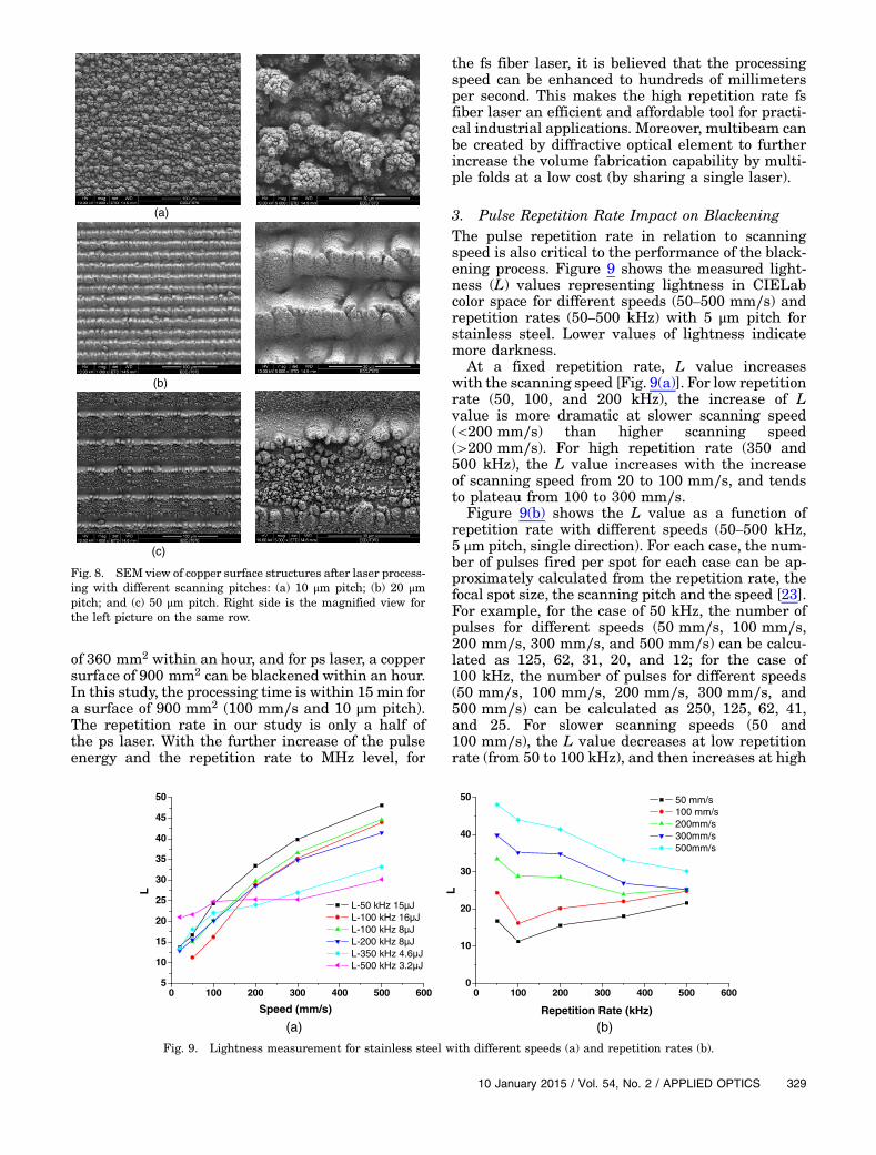
Figures 8 shows the SEM view of surface struc-tures created with different scanning pitches atthe same scanning speed (10 mm∕s). Similarly, dif-ferent kinds of microstructures can be introducedonto the sample surfaces with the scanning pitchranging from smaller to greater than the focal spotdiameter. With the scanning interval being muchsmaller than the focal spot diameter, the entire areawas processed with pulse overlap rate (i.e., repetitionrate/scanning speed) around 625 pulses per spot,coral-like surface structures with microcavities wereproduced. These structures seem self-assembledwith random orientations [Fig. 8(a)]. The microcav-ities consist of small holes with dimensions of1–10 μm, forming a porous structure. When the scan-ning pitch was close to the focal spot diameter, bellmouth-like structures were fabricated [Fig. 8(b)].When the scanning pitch was larger than the focalspot diameter, only a certain portion of the surfacewas irradiated directly by the laser focus spot, andshallow trenches were created crossing each otherand microparticles and nanoparticles were seen inthe trenches [Fig. 8(c)]. Meanwhile, it is found thatunlike aluminum sample, the porous structure onthe copper surface looks more like explosion wheremicroparticles and nanoparticles are randomly dis-tributed on each exploded surface and inside thehole, whereas the porous structure in aluminum sur-faces looks like etching and the small particles arealso randomly distributed on each surface and insidethe hole.
Furthermore, the processing efficiency and perfor-mance in this study was also compared with theexperimental results using other types of lasers, suchas ps [23] laser and solid-state fs laser [6]. It is inspir-ing to see that to achieve the total reflectance close toother lasers for the visible spectral range, theprocessing efficiency in this study is at least 8 timeshigher than the fs laser source and twice as high asthe ps laser sources. The solid-state fs laser process-ing can blacken the aluminum surface with an area
Fig. 7. (a) Reflectance as a function of wavelength for copper samples with different scanning pitches. For comparison, the reflectance ofpolished copper surface is also plotted. (b) Reflectance as a function of wavelength for copper samples with different scanning speeds.
328 APPLIED OPTICS / Vol. 54, No. 2 / 10 January 2015
of 360 mm2 within an hour, and for ps laser, a coppersurface of 900 mm2 can be blackened within an hour.In this study, the processing time is within 15 min fora surface of 900 mm2 (100 mm∕s and 10 μm pitch).The repetition rate in our study is only a half ofthe ps laser. With the further increase of the pulseenergy and the repetition rate to MHz level, for
the fs fiber laser, it is believed that the processingspeed can be enhanced to hundreds of millimetersper second. This makes the high repetition rate fsfiber laser an efficient and affordable tool for practi-cal industrial applications. Moreover, multibeam canbe created by diffractive optical element to furtherincrease the volume fabrication capability by multi-ple folds at a low cost (by sharing a single laser).
3. Pulse Repetition Rate Impact on BlackeningThe pulse repetition rate in relation to scanningspeed is also critical to the performance of the black-ening process. Figure 9 shows the measured light-ness (L) values representing lightness in CIELabcolor space for different speeds (50–500 mm∕s) andrepetition rates (50–500 kHz) with 5 μm pitch forstainless steel. Lower values of lightness indicatemore darkness.
At a fixed repetition rate, L value increaseswith the scanning speed [Fig. 9(a)]. For low repetitionrate (50, 100, and 200 kHz), the increase of Lvalue is more dramatic at slower scanning speed(<200 mm∕s) than higher scanning speed(>200 mm∕s). For high repetition rate (350 and500 kHz), the L value increases with the increaseof scanning speed from 20 to 100 mm∕s, and tendsto plateau from 100 to 300 mm∕s.
Figure 9(b) shows the L value as a function ofrepetition rate with different speeds (50–500 kHz,5 μm pitch, single direction). For each case, the num-ber of pulses fired per spot for each case can be ap-proximately calculated from the repetition rate, thefocal spot size, the scanning pitch and the speed [23].For example, for the case of 50 kHz, the number ofpulses for different speeds (50 mm∕s, 100 mm∕s,200 mm∕s, 300 mm∕s, and 500 mm∕s) can be calcu-lated as 125, 62, 31, 20, and 12; for the case of100 kHz, the number of pulses for different speeds(50 mm∕s, 100 mm∕s, 200 mm∕s, 300 mm∕s, and500 mm∕s) can be calculated as 250, 125, 62, 41,and 25. For slower scanning speeds (50 and100 mm∕s), the L value decreases at low repetitionrate (from 50 to 100 kHz), and then increases at high
(a)
(b)
(c)
Fig. 8. SEM view of copper surface structures after laser process-ing with different scanning pitches: (a) 10 μm pitch; (b) 20 μmpitch; and (c) 50 μm pitch. Right side is the magnified view forthe left picture on the same row.
5
10
15
20
25
30
35
40
45
50
L
Speed (mm/s)
L-50 kHz 15µJ L-100 kHz 16µJ L-100 kHz 8µJ L-200 kHz 8µJ L-350 kHz 4.6µJ L-500 kHz 3.2µJ
0 100 200 300 400 500 600 0 100 200 300 400 500 6000
10
20
30
40
50
L
Repetition Rate (kHz)
50 mm/s 100 mm/s 200mm/s 300mm/s 500mm/s
(b)(a)
Fig. 9. Lightness measurement for stainless steel with different speeds (a) and repetition rates (b).
10 January 2015 / Vol. 54, No. 2 / APPLIED OPTICS 329
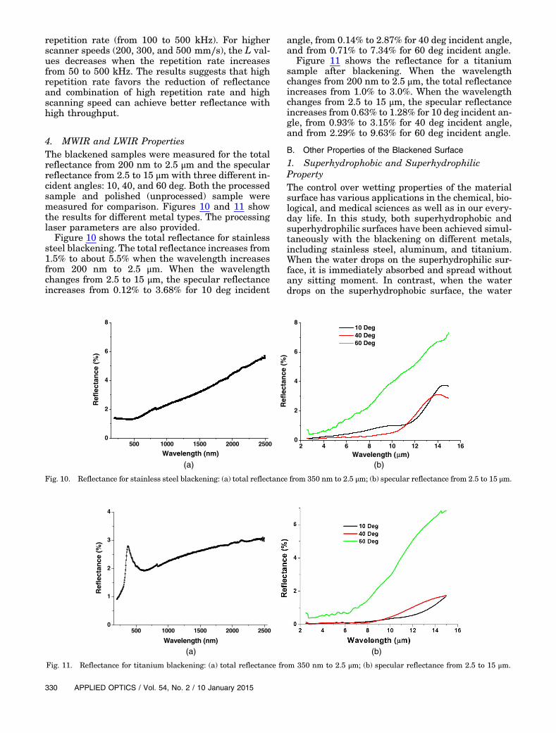
repetition rate (from 100 to 500 kHz). For higherscanner speeds (200, 300, and 500 mm∕s), the L val-ues decreases when the repetition rate increasesfrom 50 to 500 kHz. The results suggests that highrepetition rate favors the reduction of reflectanceand combination of high repetition rate and highscanning speed can achieve better reflectance withhigh throughput.
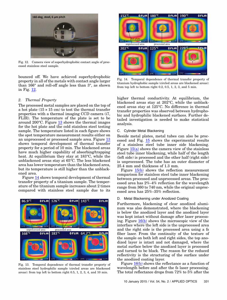
4. MWIR and LWIR PropertiesThe blackened samples were measured for the totalreflectance from 200 nm to 2.5 μm and the specularreflectance from 2.5 to 15 μm with three different in-cident angles: 10, 40, and 60 deg. Both the processedsample and polished (unprocessed) sample weremeasured for comparison. Figures 10 and 11 showthe results for different metal types. The processinglaser parameters are also provided.
Figure 10 shows the total reflectance for stainlesssteel blackening. The total reflectance increases from1.5% to about 5.5% when the wavelength increasesfrom 200 nm to 2.5 μm. When the wavelengthchanges from 2.5 to 15 μm, the specular reflectanceincreases from 0.12% to 3.68% for 10 deg incident
angle, from 0.14% to 2.87% for 40 deg incident angle,and from 0.71% to 7.34% for 60 deg incident angle.
Figure 11 shows the reflectance for a titaniumsample after blackening. When the wavelengthchanges from 200 nm to 2.5 μm, the total reflectanceincreases from 1.0% to 3.0%. When the wavelengthchanges from 2.5 to 15 μm, the specular reflectanceincreases from 0.63% to 1.28% for 10 deg incident an-gle, from 0.93% to 3.15% for 40 deg incident angle,and from 2.29% to 9.63% for 60 deg incident angle.
B. Other Properties of the Blackened Surface
1. Superhydrophobic and SuperhydrophilicPropertyThe control over wetting properties of the materialsurface has various applications in the chemical, bio-logical, and medical sciences as well as in our every-day life. In this study, both superhydrophobic andsuperhydrophilic surfaces have been achieved simul-taneously with the blackening on different metals,including stainless steel, aluminum, and titanium.When the water drops on the superhydrophilic sur-face, it is immediately absorbed and spread withoutany sitting moment. In contrast, when the waterdrops on the superhydrophobic surface, the water
2 4 6 8 10 12 14 160
2
4
6
8
Ref
lect
ance
(%
)
Wavelength (μm)
10 Deg 40 Deg 60 Deg
500 1000 1500 2000 25000
2
4
6
8
Ref
lect
ance
(%
)
Wavelength (nm)
(a) (b)
Fig. 10. Reflectance for stainless steel blackening: (a) total reflectance from 350 nm to 2.5 μm; (b) specular reflectance from 2.5 to 15 μm.
500 1000 1500 2000 25000
1
2
3
4
Ref
lect
ance
(%
)
Wavelength (nm)
(b)(a)
Fig. 11. Reflectance for titanium blackening: (a) total reflectance from 350 nm to 2.5 μm; (b) specular reflectance from 2.5 to 15 μm.
330 APPLIED OPTICS / Vol. 54, No. 2 / 10 January 2015
bounced off. We have achieved superhydrophobicproperty in all of the metals with contact angle largerthan 166° and roll-off angle less than 3°, as shownin Fig. 12.
2. Thermal PropertyThe processed metal samples are placed on the top ofa hot plate (15 × 15 cm) to test the thermal transferproperties with a thermal imaging CCD camera (i7,FLIR). The temperature of the plate is set to bearound 200°C. Figure 13 shows the thermal imagesfor the hot plate and the cold stainless steel testingsample. The temperature listed in each figure showsthe spot temperature measurement results either onan unprocessed or processed sample area. Figure 13shows temporal development of thermal transferproperty for a period of 10 min. The blackened areashave much higher capability of absorbing/trappingheat. At equilibrium they stay at 183°C, while theunblackened areas stay at 65°C. The less blackenedarea has lower temperature than the blackened area,but its temperature is still higher than the unblack-ened area.
Figure 14 shows temporal development of thermaltransfer property of a titanium sample. The temper-ature of the titanium sample increases about 2 timescompared with stainless steel sample due to its
higher thermal conductivity. At equilibrium, theblackened areas stay at 202°C, while the unblack-ened areas stay at 125°C. No difference in thermaltransfer properties was observed between hydropho-bic and hydrophilic blackened surfaces. Further de-tailed investigation is needed to make statisticalanalysis.
C. Cylinder Metal Blackening
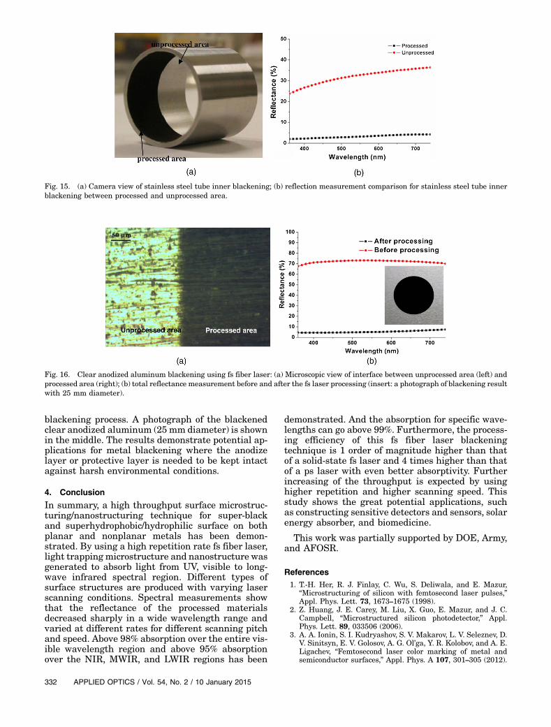
Beside metal plates, metal tubes can also be proc-essed and Fig. 15 shows the experimental resultsof a stainless steel tube inner side blackening.Figure 15(a) shows the camera view of the stainlesssteel tube inner blackening, while half of the length(left side) is processed and the other half (right side)is unprocessed. The tube has an outer diameter of25.4 mm and thickness of 1.3 mm.
Figure 15(b) shows the reflection measurementcomparison for stainless steel tube inner blackeningbetween processed and unprocessed areas. The proc-essed area has 2%–4% reflection for the wavelengthrange from 360 to 740 nm, while the original unproc-essed area has 25%–35% reflection.
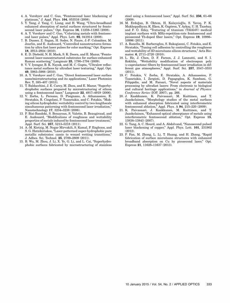
D. Metal Blackening under Anodized Coating
Furthermore, blackening of clear anodized alumi-num was also demonstrated, where the blackeningis below the anodized layer and the anodized layerwas kept intact without damage after laser process-ing. Figure 16(b) shows the microscopic view of theinterface where the left side is the unprocessed areaand the right side is the processed area using a fsfiber laser. From the continuity of the texture ofthe sample on both left and right sides, the top ano-dized layer is intact and not damaged, where themetal surface below the anodized layer is processedand turned to be black. The reason for the reducedreflectivity is the structuring of the surface underthe anodized coating layer.
Figure 16(b) shows the reflectance as a function ofwavelength before and after the fs laser processing.The total reflectance drops from 72% to 5% after the
Fig. 12. Camera view of superhydrophobic contact angle of proc-essed stainless steel sample.
unprocessed area processed area
hot plate
Fig. 13. Temporal dependence of thermal transfer property ofstainless steel hydrophilic sample (circled areas are blackenedareas): from top left to bottom right 0.5, 1, 2, 3, 4, and 10 min.
hot plate
unprocessed area processed area
Fig. 14. Temporal dependence of thermal transfer property oftitanium hydrophobic sample (circled areas are blackened areas):from top left to bottom right 0.2, 0.5, 1, 2, 3, and 5 min.
10 January 2015 / Vol. 54, No. 2 / APPLIED OPTICS 331
blackening process. A photograph of the blackenedclear anodized aluminum (25 mm diameter) is shownin the middle. The results demonstrate potential ap-plications for metal blackening where the anodizelayer or protective layer is needed to be kept intactagainst harsh environmental conditions.
4. Conclusion
In summary, a high throughput surface microstruc-turing/nanostructuring technique for super-blackand superhydrophobic/hydrophilic surface on bothplanar and nonplanar metals has been demon-strated. By using a high repetition rate fs fiber laser,light trapping microstructure and nanostructure wasgenerated to absorb light from UV, visible to long-wave infrared spectral region. Different types ofsurface structures are produced with varying laserscanning conditions. Spectral measurements showthat the reflectance of the processed materialsdecreased sharply in a wide wavelength range andvaried at different rates for different scanning pitchand speed. Above 98% absorption over the entire vis-ible wavelength region and above 95% absorptionover the NIR, MWIR, and LWIR regions has been
demonstrated. And the absorption for specific wave-lengths can go above 99%. Furthermore, the process-ing efficiency of this fs fiber laser blackeningtechnique is 1 order of magnitude higher than thatof a solid-state fs laser and 4 times higher than thatof a ps laser with even better absorptivity. Furtherincreasing of the throughput is expected by usinghigher repetition and higher scanning speed. Thisstudy shows the great potential applications, suchas constructing sensitive detectors and sensors, solarenergy absorber, and biomedicine.
This work was partially supported by DOE, Army,and AFOSR.
References1. T.-H. Her, R. J. Finlay, C. Wu, S. Deliwala, and E. Mazur,
“Microstructuring of silicon with femtosecond laser pulses,”Appl. Phys. Lett. 73, 1673–1675 (1998).
2. Z. Huang, J. E. Carey, M. Liu, X. Guo, E. Mazur, and J. C.Campbell, “Microstructured silicon photodetector,” Appl.Phys. Lett. 89, 033506 (2006).
3. A. A. Ionin, S. I. Kudryashov, S. V. Makarov, L. V. Seleznev, D.V. Sinitsyn, E. V. Golosov, A. G. Ol’ga, Y. R. Kolobov, and A. E.Ligachev, “Femtosecond laser color marking of metal andsemiconductor surfaces,” Appl. Phys. A 107, 301–305 (2012).
Fig. 15. (a) Camera view of stainless steel tube inner blackening; (b) reflection measurement comparison for stainless steel tube innerblackening between processed and unprocessed area.
Fig. 16. Clear anodized aluminum blackening using fs fiber laser: (a) Microscopic view of interface between unprocessed area (left) andprocessed area (right); (b) total reflectance measurement before and after the fs laser processing (insert: a photograph of blackening resultwith 25 mm diameter).
332 APPLIED OPTICS / Vol. 54, No. 2 / 10 January 2015
4. A. Vorobyev and C. Guo, “Femtosecond laser blackening ofplatinum,” J. Appl. Phys. 104, 053516 (2008).
5. Y. Yang, J. Yang, C. Liang, and H. Wang, “Ultra-broadbandenhanced absorption of metal surfaces structured by femto-second laser pulses,” Opt. Express 16, 11259–11265 (2008).
6. A. Y. Vorobyev and C. Guo, “Colorizing metals with femtosec-ond laser pulses,” Appl. Phys. Lett. 92, 041914 (2008).
7. B. Dusser, Z. Sagan, H. Soder, N. Faure, J.-P. Colombier, M.Jourlin, and E. Audouard, “Controlled nanostructures forma-tion by ultra fast laser pulses for color marking,” Opt. Express18, 2913–2924 (2010).
8. E. D. Diebold, N. H. Mack, S. K. Doorn, and E. Mazur, “Femto-second laser-nanostructured substrates for surface-enhancedRaman scattering,” Langmuir 25, 1790–1794 (2009).
9. V. V. Iyengar, B. K. Nayak, and M. C. Gupta, “Ultralow reflec-tance metal surfaces by ultrafast laser texturing,” Appl. Opt.49, 5983–5988 (2010).
10. A. Y. Vorobyev and C. Guo, “Direct femtosecond laser surfacenano/microstructuring and its applications,” Laser PhotonicsRev. 7, 385–407 (2013).
11. T. Baldacchini, J. E. Carey, M. Zhou, and E. Mazur, “Superhy-drophobic surfaces prepared by microstructuring of siliconusing a femtosecond laser,” Langmuir 22, 4917–4919 (2006).
12. V. Zorba, L. Persano, D. Pisignano, A. Athanassiou, E.Stratakis, R. Cingolani, P. Tzanetakis, and C. Fotakis, “Mak-ing silicon hydrophobic: wettability control by two-lengthscalesimultaneous patterning with femtosecond laser irradiation,”Nanotechnology 17, 3234–3238 (2006).
13. P. Bizi-Bandoki, S. Benayoun, S. Valette, B. Beaugiraud, andE. Audouard, “Modifications of roughness and wettabilityproperties of metals induced by femtosecond laser treatment,”Appl. Surf. Sci. 257, 5213–5218 (2011).
14. A.-M. Kietzig, M. Negar Mirvakili, S. Kamal, P. Englezos, andS. G. Hatzikiriakos, “Laser-patterned super-hydrophobic puremetallic substrates: cassie to wenzel wetting transitions,”J. Adhes. Sci. Technol. 25, 2789–2809 (2011).
15. B. Wu, M. Zhou, J. Li, X. Ye, G. Li, and L. Cai, “Superhydro-phobic surfaces fabricated by microstructuring of stainless
steel using a femtosecond laser,” Appl. Surf. Sci. 256, 61–66(2009).
16. M. Erdoğan, B. Öktem, H. Kalaycioğlu, S. Yavaş, P. K.Mukhopadhyay, K. Eken, K. Özgören, Y. Aykaç, U. H. Tazebay,and F. Ö. Ilday, “Texturing of titanium (Ti6Al4V) medicalimplant surfaces with MHz-repetition-rate femtosecond andpicosecond Yb-doped fiber lasers,” Opt. Express 19, 10986–10996 (2011).
17. A. Ranella, M. Barberoglou, S. Bakogianni, C. Fotakis, and E.Stratakis, “Tuning cell adhesion by controlling the roughnessand wettability of 3Dmicro/nano silicon structures,” Acta Bio-mater. 6, 2711–2720 (2010).
18. L. He, J. Chen, D. F. Farson, J. J. Lannutti, and S. I.Rokhlin, “Wettability modification of electrospun poly(ε-caprolactone) fibers by femtosecond laser irradiation in dif-ferent gas atmospheres,” Appl. Surf. Sci. 257, 3547–3553(2011).
19. C. Fotakis, V. Zorba, E. Stratakis, A. Athanassiou, P.Tzanetakis, I. Zergioti, D. Papagoglou, K. Sambani, G.Filippidis, and M. Farsari, “Novel aspects of materialsprocessing by ultrafast lasers: From electronic to biologicaland cultural heritage applications,” in Journal of Physics:Conference Series (IOP, 2007), pp. 266.
20. J. Kaakkunen, K. Paivasaari, M. Kuittinen, and T.Jaaskelainen, “Morphology studies of the metal surfaceswith enhanced absorption fabricated using interferometricfemtosecond ablation,” Appl. Phys. A 94, 215–220 (2009).
21. K. Paivasaari, J. Kaakkunen, M. Kuittinen, and T.Jaaskelainen, “Enhanced optical absorptance of metals usinginterferometric femtosecond ablation,” Opt. Express 15,13838–13843 (2007).
22. G. Tang, A. C. Hourd, and A. Abdolvand, “Nanosecond pulsedlaser blackening of copper,” Appl. Phys. Lett. 101, 231902(2012).
23. P. Fan, M. Zhong, L. Li, T. Huang, and H. Zhang, “Rapidfabrication of surface micro/nano structures with enhancedbroadband absorption on Cu by picosecond laser,” Opt.Express 21, 11628–11637 (2013).
10 January 2015 / Vol. 54, No. 2 / APPLIED OPTICS 333