BLAB3 Design review
58
Buffered LABRADOR (BLAB3) Design Review Gary S. Varner 4 NOV 09
Transcript of BLAB3 Design review

Buffered LABRADOR (BLAB3) Design Review
Gary S. Varner 4 NOV 09

Goals for today• Baseline confirmation
– Ice Radio Sampler (IRS) as sampling/storage array basis
– High rate/long latency architecture
• Review simulations– Basic functionality– Additional monitor/control features
• Flag action items (prior to submission)– Anything missing? – Target submission (26 OCT 09 delayed) [23 NOV 09]

BLAB3 Specifications32768 samples/chan (>5us trig latency)
8 channels/BLAB3 ASIC8 Trigger channels
~9 bits resolution (12[10]-bits logging)64 samples convert window (~16ns)4 GSa/s1 word (RAM) chan, sample readout
1+n*0.02 us to read n samples (of same 64)30 kHz sustained readout (multibuffer)
• Time alignment critical– Synchronize sampling to accelerator RF clock
– >5us a must for trigger, since single photon rates high
• Needs Gain!

Gain Needed
• What gain needed?– At 106 gain, each p.e. = 160 fC
– At 2x10⁵ gain (better for aging), each p.e. = 32 fC
– In typical ~5ns pulse, Vpeak = dQ/dt * R = 32uA * R = 32mV * R [kΩ] (6.4mV)
Amplifiers dominate board space
Readout ASIC pair
Rterm 1 p.e. peak50 1mV1k 20mV
20k 400mV
Gain Estimate

Starting place: IRS design
• 8 HS inputs• 64 x 2 samples/ch• 32k deep storage• 64 sample select• 8x64 Wilk ADC
• 12 output bits• Random Access• 10-bits Write Sel• 10-bits Read Sel• 3-bits channel• 7-bits ADC ch• 129 bonding pads• 180um min pitch

BLAB3Single Channel
• Storage: 64 x 512 (512 = 8 * 64)
• Sampling: 128 (2x 64) separate transfer lanes
Recording in one set 64, transferring other (“ping-pong”)
• Wilkinson (32x2): 64 conv/channel

IRS Input Coupling
• Input bandwidth depends on 2x terms– f3dB[input] = [2*π*Z*Ctot]-1
– f3dB[storage] = [2*π*Ron*Cstore]-1
Input Coupling versus total input Capacitance
0
0.5
1
1.5
2
2.5
3
3.5
0 500 1000 1500 2000 2500 3000
Total input Capacitance [fF]
Anal
og B
andw
idth
[-3d
B fre
quen
cy]
R_S = 50Ohm
Input coupling versus frequency
-10
-9
-8
-7
-6
-5
-4
-3
-2
-1
0
0.1 1 10 100
Frequency [GHz]Re
lativ
e am
plitu
de [d
B]
C=15fF,Ron=1kC=15fF,Ron=5kC=25fF,Ron=1kC=25fF,Ron=5k

IRS Input Coupling
• Role of inductance
Input inductance impedance versus frequency
0
20
40
60
80
100
120
140
160
180
200
0.1 1 10 100
Frequency [GHz]
Impe
danc
e [O
hms]
Bond-wireBump-bond
Input coupling versus frequency
-10
-8
-6
-4
-2
0
2
4
6
8
10
0.1 1 10 100
Frequency [GHz]
Rel
ativ
e am
plitu
de [d
B]
Bond-wireBump-bond

Input coupling sim (35fF sample)
~1 GHz analog bandwidthInto storage cell
Onto chip

Trans-Impedance Amp
• Basic building block have used before

3kΩ TIA Sim
~380MHz analog bandwidth

TIA timing simulation results
• Some overshoot – a realistic current pulse?

Summary Plot ABW
TIA Analog Bandwidth vs. Gain
0
50
100
150
200
250
300
350
400
450
1 10 100
TIA Gain [k-Ohm]
Anal
og B
andw
idth
[MHz
]
100uA60x gain

TIA Analog Bandwidth vs. Gain
0
50
100
150
200
250
300
350
400
450
500
1 10 100 1000 10000
Bias Current [uA]
Anal
og B
andw
idth
[MHz
]
3k TIA
Summary Plot ABW vs. Bias
Saturates ~500uA

Simulated Noise
Saturates ~500uA
Input noise
Output noise
Noise integral from 100.00000K Hz to 1.00000G HzTotal integrated output noise voltage = 42.96911u VTotal equivalent input noise voltage = 992.82668u V

Phase Response
~300MHz

Sample Cell
• Main element is buffer amp (OTA)– Relatively low current (10’s uA) operation possible

Effect of too small a storage CapDesire small C for better Input Coupling
Cstore = 35fF

Storage Cell
• Diff. Pair as comparator– Only power on selected block

Another Constraint: Leakage Current
Can Improve? (readout faster)
Need small C for Input Coupling
Sample channel-channel variation ~ fA leakage typically

Sample transfer – realistic capacitance
• 200Ω isolation resistor to reduce ringing
• <= 16ns settling

IRS Sampling Method
• Base delay

Sampling Simulation with full parasitic Extraction
0.000
0.500
1.000
1.500
2.000
2.500
3.000
3.500
4.000
4.500
5.000
0 0.5 1 1.5 2 2.5
RCObias [V]
Sam
plin
g R
ate
[GSa
/s]
Extracted
Simulated sampling speed
“RCObias” VadjP1,2 = RCObias; VadjN1,2 = VDD-RCObias

Triggering
• Need 9th channel for monitoring

Temperature Dependence
0.2%/degree C(can correct)
6GSa/sSample aperature (172ps = 5.8GSa/s)
Matches SPICE simulation

Triggering – same as previous resultsTrigger 1-shot Width Adjust
1
10
100
0 20 40 60 80 100 120
Discharge Current [uA]
Out
put W
idth
[ns]
T_1_TRGPower (T_1_TRG)
• Monitor 9th channel (uses Ch.1 threshold) to compensate for temperature dependence

BLAB3 Digitization
• Excellent linearity• Basically as good as can make current
source/comparator
12-bit ADC
• No missing codes
• Linearity as good as can make ramp
• Can bracket range of
interest
Run count during ramp
Wilkinson ADC
Modified! (self-counter)[~0.7 GHz]

Wilkinson Clock Generation
• Strictly only 5 channels necessary– 4x antenna, 1x reference channels
– Could interleave for twice depth, or multiple reference channels

Wilkinson Recording
Start = start 0.5-1.5GHz Clock Ripple counter (run as fast as can)
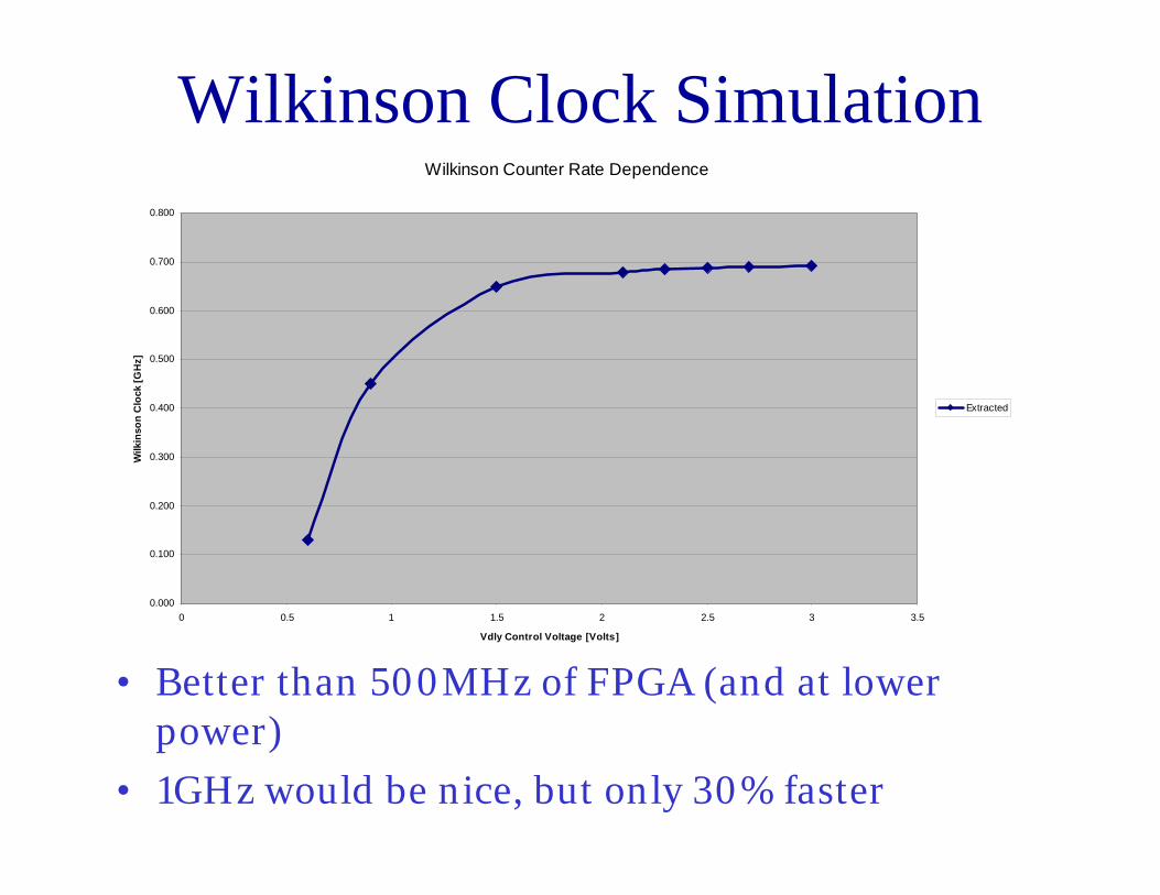
Wilkinson Clock SimulationWilkinson Counter Rate Dependence
0.000
0.100
0.200
0.300
0.400
0.500
0.600
0.700
0.800
0 0.5 1 1.5 2 2.5 3 3.5
Vdly Control Voltage [Volts]
Wilk
inso
n C
lock
[GH
z]
Extracted
• Better than 500MHz of FPGA (and at lower power)
• 1GHz would be nice, but only 30% faster

Simulated transfer encoding
Works as expected

Output Bus Settling Time
~100MHz bus operation should be possible
~8.5ns (10-90%)

9.5mm7.62mm
Project# 80350 (BLAB3) Wirebonding diagram
Design_number: 80350Customer name: Univ. of HawaiiCustomer acct: 2105Phone number: (808) 956-2987Fax number: (808) 956-2930Qty packaged: 0 Package name: LQFP128ACavity size: 9.5mm x 9.5mm
MOSIS ID
9.5mm5.82mm
NOTE: pads 33, 63, 64, 97, 98, 128
are NOT bonded

Summary• Leveraging IRS design effort
– ~0.4 GHz analog bandwidth
– All basic functionality simulates OK (with parasitics)
– Up to 100MHz bus readout rate (50MHz conservative)
• Am concerned about schedule… – Things will be much worse if doesn’t work– Could put in 128pin package– Matters if will stud bond?
• Remaining concerns– Optimal Write Address selection time– Noise level on input– Cost of stud bonding– Others from today?

2.6m
1.2m
e-
8.0GeVe+
3.5GeV
Barrel PID Aerogel RICH
- PID (π/Κ) detectors- Inside current calorimeter- Use less material and allow more tracking volume
Available geometry defines form factor-
Upgraded detector

Bars compatible (though thinner)with proposed TOP counter
Concept: Use best of both TOP (timing) and DIRC and fit in Belle PID envelope
• Use new, compact solid-state photon detectors, new high-density electronics• Use simultaneous T, θc [measured-predicted] for maximum K/π separation• Keep pixel size comparable to DIRC
BaBar DIRC
Drawing by Marc Rosen(UH)
imaging TOP (iTOP)

Proposed Common Approach for Belle2

Baseline image block
Top View2x 64-channel PMTs per fiber link
7x BLAB3 daughtercards (112x BLAB3)896 PMT channels/module (16 iTOP staves)
7 data, 7 trigger fiber pairs + HV power, LVDS RF clock, Revolution marker pairs

Baseline System Components
• BLAB3 is 8 channels, each 32k samples deep
• <~1us to read out 32-samples hit/BLAB3
Photo-Sensor
BLAB3
BLAB3
BLAB3
BLAB3
MCP
MAIN FINESSE
CARD
x4COPPER
FIFO
Giga-bit
Fiber
Total channel numbers presented previously unchanged, partitioned
slightly differently
Photo-Sensor
x4

Hit Processing reminder Assume:100kHz charged track hits on each bar
~32 p.e./track (1% of 100ns windows)30kHz trigger rate
Each PMT pair sees <8> hits240k hits/s
Each BLAB3 has an average occupancy <1 hit (assume 1)
400ns to convert 256 samples16ns/sample to transfer
At least 16 deep buffering(Markov overflow probability
est. < 10-38)
Each hit = 64samples * 8bits = 512bits~125Mbits/s
(link is 3.0 Gb/s ~ x30 margin)
BLAB3 ASIC
8
Trans-Imp Amps 512 x 64 samples
Per channel
Fast conversionMatrix (x256)
BLAB3 sampling
Improvements based uponLessons learned from BLAB2
Plan to model in standard queuing simulator, but looks like no problem(CF have done same exercise with Jerry Va’vra for 150kHz L1 of SuperB and can handle rate)

Context: BLAB2 & “PD scale” readout• Initial Target: New f-DIRC Readout System
Really reached on specs…
Gen. 0 Prototype (LAB3)

BLAB2 Lessons• RGC (Regulated Cascode)
– Fussy – doesn’t look like 50Ω for large voltage signals
– Not enough phase margin (oscillates)
• Sampling– nMOS/pMOS does NOT work
– Alignment between sampling rows
– Overall timing alignment troublesome
– Better with fewer distinct samples, yet having more buffer depth

• 448 channels readout at SLAC + few hundred UH [HI-TIDE]• Learning about big system timing issues
Experiment 2: 13-Mar-09 – (~9 mo.)
Experiment 3: winter – (~6+ mo.)• BLAB3 ASIC upgrade (lessons learned)• At speed fast feature extraction

1kΩ TIA Sim
~405MHz analog bandwidth

2kΩ TIA Sim
~400MHz analog bandwidth

5kΩ TIA Sim
~350MHz analog bandwidth

10kΩ TIA Sim
~300MHz analog bandwidth

20kΩ TIA Sim
~245MHz analog bandwidth

50kΩ TIA Sim
~170MHz analog bandwidth

100kΩ TIA Sim
~130MHz analog bandwidth

3kΩ TIA, bias current sims
~130MHz analog bandwidth

3kΩ TIA, bias current sims
~200MHz analog bandwidth

3kΩ TIA, bias current sims
~300MHz analog bandwidth

3kΩ TIA, bias current sims
~370MHz analog bandwidth

3kΩ TIA, bias current sims
~420MHz analog bandwidth

3kΩ TIA, bias current sims
~450MHz analog bandwidth

3kΩ TIA, bias current sims
~450MHz analog bandwidth

3kΩ TIA, bias current sims
~450MHz analog bandwidth