Basic operation of a (Heterojunction) Bipolar Transistor ...
description

Lecture:Thebipolartransistor
1.1 – The planar bipolar transistor
The bipolar transistor was invented in 1947 by W.Shockley, J.Bardeen and W.Brattain. The device is characterized by an exponential link between the collector current and the potential difference between the base and emitter terminals (Figure 1):
⋅= ⋅ BEq V kT
C SI I e
where IS is the inverse saturation current.
Figure 1 – npn Bipolar Transistor: (a) symbol, (b) minority carrier profile (electrons) in the base region.
When the npn transistor operates in the active region (Figure 1) electrons are injected into the base from the forward-bias base-emitter junction. They diffuse until reaching the collector leading to a current density given by:
(0) ( )−= ⋅ ⋅ B
nn
B
n n WJ q D
W
Since the base-collector junction is biased in reverse region, n(WB)≅0 and then,
2
= ⋅ ⋅ =BE BEqV kT qV kTin
n S
B B
nJ q D e J e
N W
where Js is the saturation current density. Figure 2 shows the classical structure of a planar bipolar transistor. The device is made in an n epitaxial layer, grown on a p substrate. The p-doped base and the n+ emitter are obtained by implantation and subsequent thermal annealing.
Figure 2: Cross section of a planar npn bipolar transistor

Lectures on Analog Circuit Design 2
As the base-emitter junction is forward-biased, the electrons are injected in the direction orthogonal to the wafer surface. The carriers diffuse into the base region and reach the n+ collector region. Note how the active part of the device, namely that part where the transistor effect takes place, is composed of the n+-p-n region just below the emitter diffusion. The total current due to electrons is then obtained by multiplying the current density for the emitter area:
2
= ⋅ ⋅ ⋅ =BE BEqV kT qV kTinC E S
B B
nI q D A e I e
N W
In parallel to the injection of electrons from the emitter toward the base, holes are injected from the Base into the Emitter. Since normally the emitter is much heavily doped compared to the Base, the holes flux towards the emitter is much smaller than the electron flow from the emitter. The ratio between the two currents defines the coefficient:
0.99C
E
I
Iα = ≅
therefore the device, to properly work, requires a non-zero base current IB. The ratio between the collector current and the base current defines the bipolar transistor
coefficient β:
C
B
I
Iβ =
Since the conservation equation holds between the terminals currents, it is:
E C BI I I= +
Leading to a link between the α and β parameters:
1
βα
β=
+
Typical β values for npn transistors range from 100 to 200.
The need for electrical contacts on the surface, adds additional resistive paths. For example, the collector current must reach the lateral contact along the n layer. It therefore has a distributed resistance, rcc, in series with the collector "internal" resistance. To reduce this parasitic element a buried layer is fabricated at the epi/substrate interface by implanting antimony in the p-substrate, aligned with the area that will accommodate the active region of the transistor, before the n layer epitaxial deposition. Since the entire transistor is immersed in a p-type substrate, the collector region forms a p-n junction with the latter. For proper device operation, this junction must be reverse biased. Therefore, the substrate terminal is normally connected to the lowest potential in the circuit. Also, to isolate each device from adjacent devices, the n-well hosting each transistor must be isolated from those hosting other devices. The isolation is achieved by implanting and diffusing a p-type zone from the surface (Figure 2) till reaching the substrate. The need for these isolations further increases the silicon area required to implement the component and therefore its unit cost.
Also the base current flows from the inner part of the base to the contact through a resistive path. The narrower the transistor base, which is needed to increase the maximum operative frequency of the component, the lower the cross section of this resistive path and therefore its resistance value, rbb. It will be seen in the following that this resistance leads to a significant contribution to the device electronic noise.

Lectures of Analog Cicrcut Design
3
Figure 3 shows schematically the planar view of the component. Since the active region of the bipolar transistor is set by the dopant diffusions along the vertical cross-section of the wafer, the designer can only modify the size of the emitter and hence the current capacity of the component. The thicknesses of the active layers, and in particular of the base, are defined by the fabrication processes, thus setting maximum operating frequency. The designer, by setting the emitter area, decides the reverse saturation current IS, and therefore, the current capability.
Figure 3. Planar view of a bipolar transistor.
1.2 Current gain and bias
Both the collector current and the base current depend on the factor BEqV kT
e as they are linked to the flow of electrons and holes that cross the forward-biased Emitter-Base junction. When these currents are plot on a semi-logarithmic scale, as a function of the voltage VBE, they lead to straight lines (Figure 4). The distance between the lines
corresponds to the current gain β.
Figure 4. Gummel Plot of a bipolar transistor. For VBE > 0.5V the device current gain is constant.
In general the current gain is constant over a VBE range between 0.5V and 0.8V. At lower
bias, the base current is characterized by a 2BEqV kT
e dependence. It is due to generation and recombination processes in the space-charge region of the Emitter-Base junction. This trend adds up to the diffusion process and become the dominant effect in the low- injection regime. The collector current, continues instead to be due to electrons only,

Lectures on Analog Circuit Design 4
which spread in the base and are collected at the collector side. This term therefore
retains the BEqV kT
e dependence.
The β current gain, which is the distance between the two lines in the Gummel plot,
decreases. A similar β drop happens at high currents (not shown in Fig.4) when phenomena due to high-level-injection come into play. This is the case of the so-called Kirck effect, also referred to as base-"push- out" effect.
Figure 5: Kirck Effect: (a) variation of the space-charge region at the base - collector junction and migration to the buried layer. ( b) Evolution of the electric field at the base-collector junction by HC Poon et al IEEE- TED 1969
Consider the Base-Collector junction. Figure 5 (a) schematically shows the space-charge at the ends of the junction. Since the collector doping, NC, is about a decade smaller than the base doping, NB, the size of the space charge region can be estimated as:
2ε≈ CB
C
VW
qN
where VCB is the reverse voltage at the ends of the junction. This expression, however, neglects the concentration of the free charge, electrons, coming from the base. They also contribute to the space charge in this region. Let us assume, for simplicity, that the electric fields at the junction are high enough to drive carriers at saturated velocity. Therefore the electrons concentration is given by:
≈ C
sat
Jn
qv
These charges, being negative, partly compensate the positive ions due to the ionized donors at the collector side. As a result, the size of the space charge zone is modulated by the current flowing through the device, being given by:
( )2ε
≈−
CB
C C sat
VW
q N J qv
Note that by Increasing the collector current, the size of the drained area increases,
become virtually infinite for Jc≅qvsatNC. Obviously this divergence does not take place. When the current density approaches the critical value, the electric dipole that must sustain the potential difference VCB applied between the base and collector terminals,

Lectures of Analog Cicrcut Design
5
migrates towards the "buried layer" , as shown by the results of numerical simulation in Figure 5b. In these operating conditions, the whole layer, up to the " buried layer" is full by electrons and holes are retrieved from the base to ensure electrical neutrality. Because of this effect the equivalent electrical length of the base layer increases up to the buried layer ("base push -out"). Therefore the recombination between electrons and holes
increases, the α coefficient decreases and the transistor current gain, β, drops. To provide a quantitative reference, let us consider a collector doping of 5·1016cm -3. With this value,
the critical current density at which these effects take place is about 0.8mA/µm2.
Figure 6 shows the typical trend of the current gain of the bipolar transistor. The gain trend is characterized by three regions. The region corresponding to the typical operating conditions shows a maximum and nearly constant gain. In the other two regions, at at low and high injection regimes, the gain drops. The extension of the three regions depends significantly on how the device is engineered, on the dimensions and doping of the active layers. The horizontal axis shows the device current. Indeed, since the voltage VBE sets the junction current density JC (the absolute value of the current also depends on the component area) it is good practice to keep in mind the current density interval over which
the β remains constant. In general, the gain drop due to low level injection effects occurs
for J <0.1µA/µm2 . The high- injection effects come into play for J>1mA/µm2. These values are intended as guidelines. The designer has to pay attention and check-out the characteristic values of the specific adopted technology. These values determine the emitter size. In fact, once the collector current is decided by bias considerations, the emitter area should be chosen to ensure that the current density JC=IC/AE falls within the central area, to have minimum Base current.
Figure 6. Current gain dependence on bias
1.3 - Maximum voltage gain
The transconductance is the key small signal parameter of a transistor. It is the ratio between the variation of the current at the output terminal and the variation of the control voltage . The expression for the transconductance is therefore obtained by differentiating the expression for the current:
∂= = ⋅ =
∂
BEqVC CkT
m S
BE TH
II qg I e
V kT V .
It turns out that the transconductance is proportional to the bias current. The larger the bias current and therefore the power dissipated across the device terminals, the larger the

Lectures on Analog Circuit Design 6
transconductance is and therefore the effectiveness of the device in translating the modulation of the control voltage in a current signal provided to downstream circuits. The trade-off between transconductance and bias current made possible by the active device is represented by the relationship :
1ε = =m
C TH
g
I V
This quantity defines a sort of device efficiency. In the case of bipolar transistors, unlike the MOSFET case, the parameter depends only on temperature and is equal to 1/VTH=40V
- 1 at room temperature.
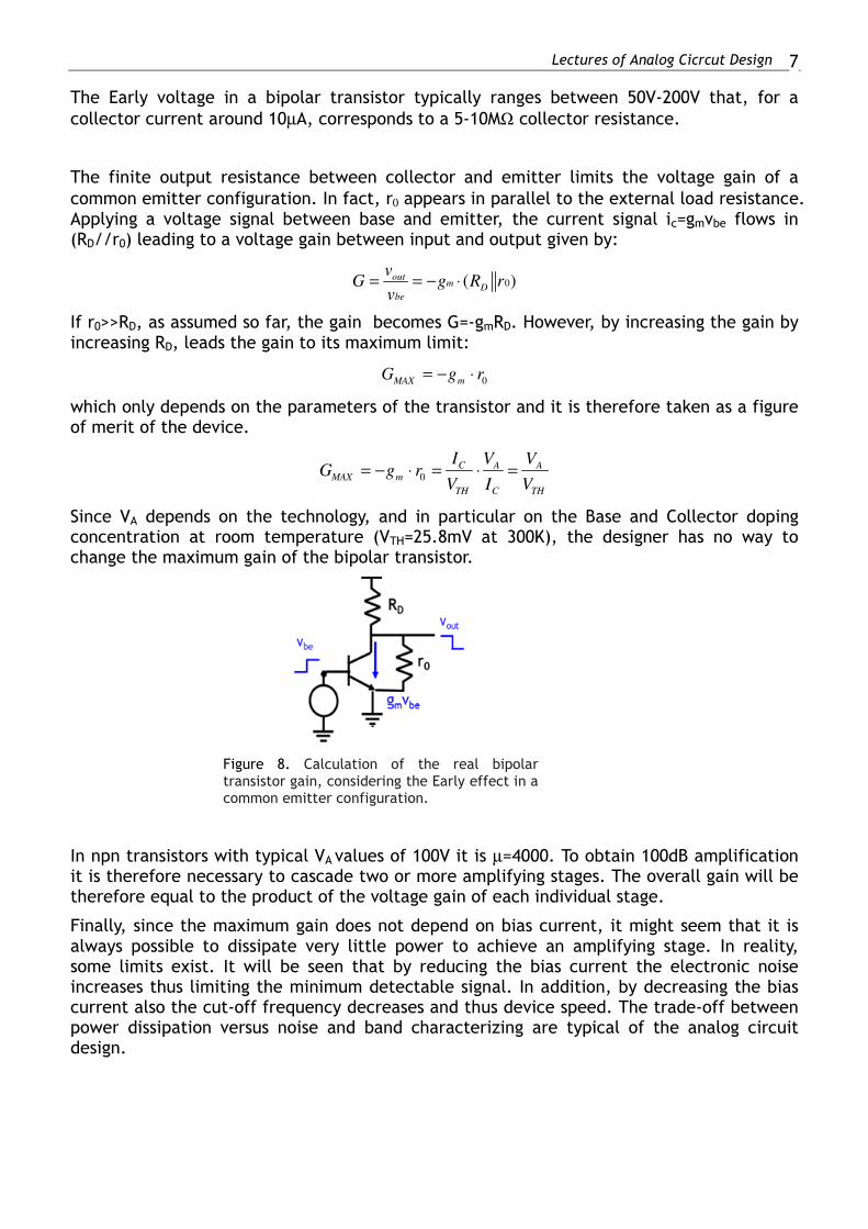
The characteristic curves in the active zone of a BJT are not perfectly parallel to the axis of the voltages (Figure 7). The collector does not behave exactly as an ideal current source, delivering a current dependent only on the Emitter-Base bias.
Figure 7. Early effect in the Bipolar transistor.
This effect, due to the modulation of the base length induced by VCE variations, is known as Early effect. Referring to the npn bipolar transistor in Figure 1, note that the voltage VCE is the sum of the voltage VBE that directly bias the base-emitter junction and voltage VCB which reversely bias the base-collector junction. As VCE increases, VBE remains constant and the VCB voltage increases. The thickness of the space charge region at the base-collector junction increases, resulting in a reduction of the thickness of the base neutral zone WB. The reverse saturation current increases and the same happens to the collector current even if the VBE remains constant.
This current dependence from the collector-emitter voltage causes the slope of the curves in the active zone that is represented in the equivalent circuit by placing a resistance r0 between the collector and emitter terminals. To minimize the Early effect the collector must be much less doped than the base so that, by increasing VCE, the junction space charge region extends mainly in the collector area, leaving almost unaltered the base size. If the characteristic I-V curves of the device in the active region in Figure 7 are extrapolated on the left-hand side to reach the VCE axis, it can be noticed that they cross the axis almost at same point -VA. The VA voltage is usually referred to as “Early voltage” and therefore the r0 value can be written as :
0= A
C
Vr
I
Lectures of Analog Cicrcut Design
7
The Early voltage in a bipolar transistor typically ranges between 50V-200V that, for a
collector current around 10µA, corresponds to a 5-10MΩ collector resistance.
The finite output resistance between collector and emitter limits the voltage gain of a
common emitter configuration. In fact, r0 appears in parallel to the external load resistance. Applying a voltage signal between base and emitter, the current signal ic=gmvbe flows in (RD//r0) leading to a voltage gain between input and output given by:
0( )outm D
be
vG g R r
v= = − ⋅
If r0>>RD, as assumed so far, the gain becomes G=-gmRD. However, by increasing the gain by increasing RD, leads the gain to its maximum limit:
0= − ⋅
MAX mG g r
which only depends on the parameters of the transistor and it is therefore taken as a figure of merit of the device.
0= − ⋅ = ⋅ =C A A
MAX m
TH C TH
I V VG g r
V I V
Since VA depends on the technology, and in particular on the Base and Collector doping concentration at room temperature (VTH=25.8mV at 300K), the designer has no way to change the maximum gain of the bipolar transistor.
Figure 8. Calculation of the real bipolar transistor gain, considering the Early effect in a common emitter configuration.
In npn transistors with typical VA values of 100V it is µ=4000. To obtain 100dB amplification it is therefore necessary to cascade two or more amplifying stages. The overall gain will be therefore equal to the product of the voltage gain of each individual stage.
Finally, since the maximum gain does not depend on bias current, it might seem that it is always possible to dissipate very little power to achieve an amplifying stage. In reality, some limits exist. It will be seen that by reducing the bias current the electronic noise increases thus limiting the minimum detectable signal. In addition, by decreasing the bias current also the cut-off frequency decreases and thus device speed. The trade-off between power dissipation versus noise and band characterizing are typical of the analog circuit design.
Lectures on Analog Circuit Design 8
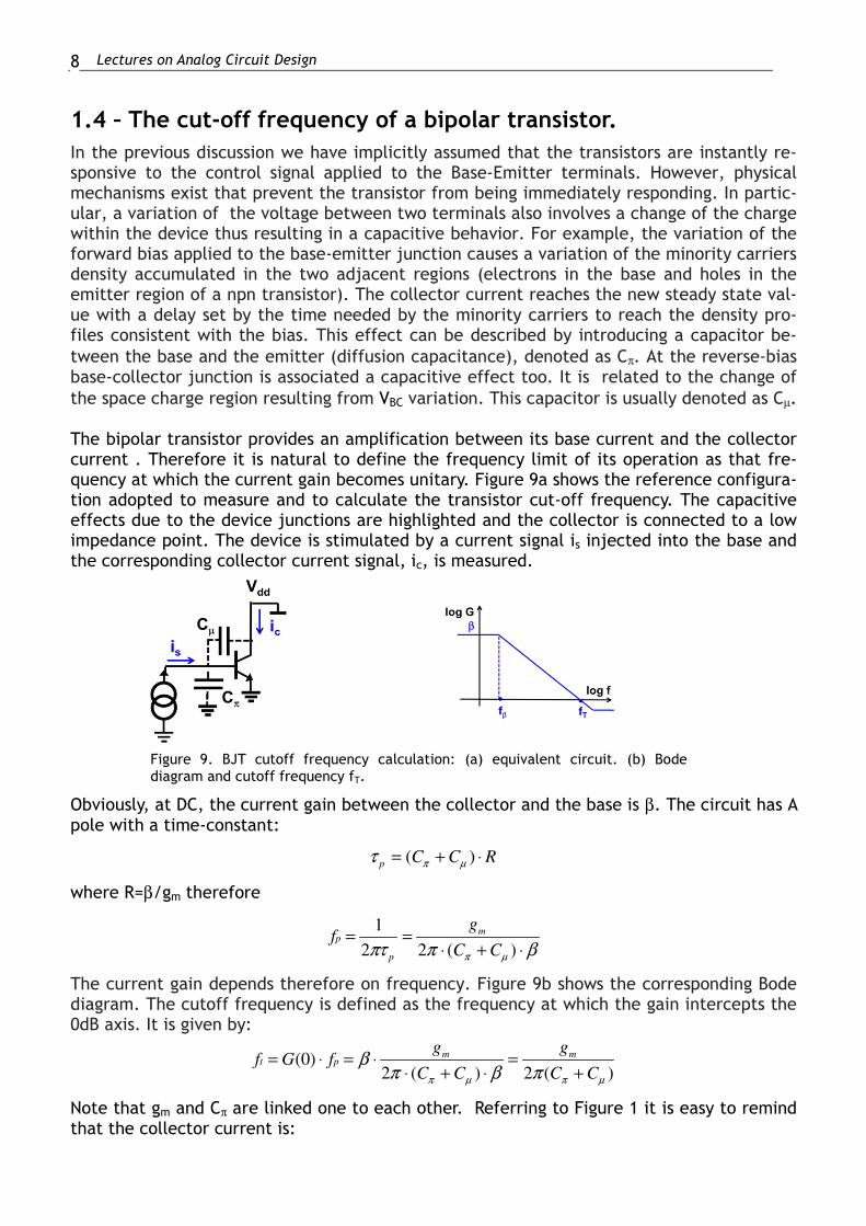
1.4 – The cut-off frequency of a bipolar transistor.
In the previous discussion we have implicitly assumed that the transistors are instantly re-sponsive to the control signal applied to the Base-Emitter terminals. However, physical mechanisms exist that prevent the transistor from being immediately responding. In partic-ular, a variation of the voltage between two terminals also involves a change of the charge within the device thus resulting in a capacitive behavior. For example, the variation of the forward bias applied to the base-emitter junction causes a variation of the minority carriers density accumulated in the two adjacent regions (electrons in the base and holes in the emitter region of a npn transistor). The collector current reaches the new steady state val-ue with a delay set by the time needed by the minority carriers to reach the density pro-files consistent with the bias. This effect can be described by introducing a capacitor be-
tween the base and the emitter (diffusion capacitance), denoted as Cπ. At the reverse-bias base-collector junction is associated a capacitive effect too. It is related to the change of
the space charge region resulting from VBC variation. This capacitor is usually denoted as Cµ. The bipolar transistor provides an amplification between its base current and the collector current . Therefore it is natural to define the frequency limit of its operation as that fre-quency at which the current gain becomes unitary. Figure 9a shows the reference configura-tion adopted to measure and to calculate the transistor cut-off frequency. The capacitive effects due to the device junctions are highlighted and the collector is connected to a low impedance point. The device is stimulated by a current signal is injected into the base and the corresponding collector current signal, ic, is measured.
Figure 9. BJT cutoff frequency calculation: (a) equivalent circuit. (b) Bode diagram and cutoff frequency fT.
Obviously, at DC, the current gain between the collector and the base is β. The circuit has A pole with a time-constant:
( )π µτ = + ⋅p
C C R
where R=β/gm therefore
1
2 2 ( )π µπτ π β= =
⋅ + ⋅m
p
p
gf
C C
The current gain depends therefore on frequency. Figure 9b shows the corresponding Bode diagram. The cutoff frequency is defined as the frequency at which the gain intercepts the 0dB axis. It is given by:
(0)2 ( ) 2 ( )π µ π µ
βπ β π
= ⋅ = ⋅ =⋅ + ⋅ +
m mt p
g gf G f
C C C C
Note that gm and Cπ are linked one to each other. Referring to Figure 1 it is easy to remind that the collector current is:
Lectures of Analog Cicrcut Design
9
(0)π= ⋅ ⋅ ⋅C E
B
nI q D A
W
The charge Q due to excess minority carriers in the Base corresponds to the area of the tri-angle defined by the electrons concentration profile, namely:
1(0)
2= ⋅ ⋅ ⋅ ⋅E BQ q A n W
The ratio between these two variables defines the average diffusion time of minority carriers in the base:
2
2τ = =
⋅B
diff
C n
WQ
I D
Note that this quantity depends quadratically on the thickness of the neutral base. Recalling that:
π=BE
dQC
dV,
=C
m
BE
dIg
dV ,
one can conclude that:
πτ =diff
m
C
g.
The fT expression therefore becomes:
1
2µ
π τ
=
⋅ +
T
diff
m
fC
g
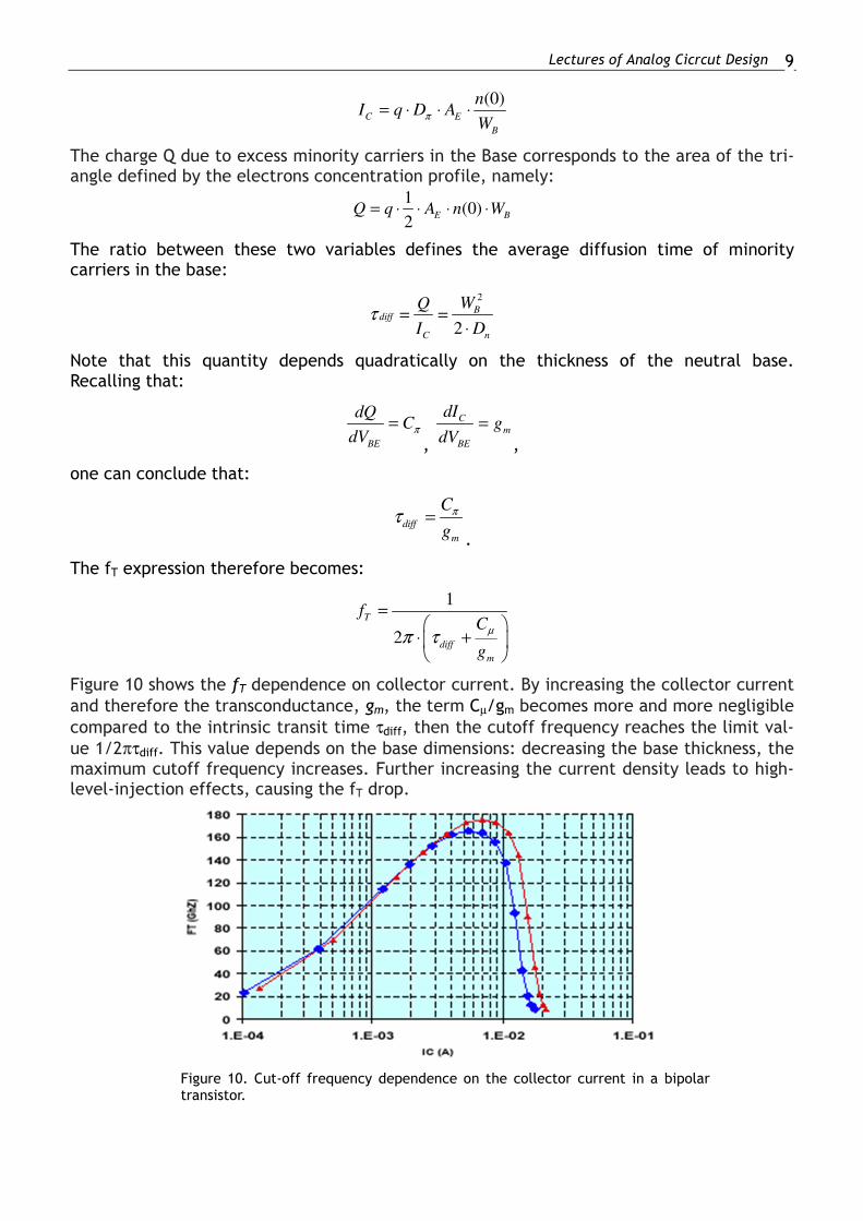
Figure 10 shows the fT dependence on collector current. By increasing the collector current
and therefore the transconductance, gm, the term Cµ/gm becomes more and more negligible
compared to the intrinsic transit time τdiff, then the cutoff frequency reaches the limit val-
ue 1/2πτdiff. This value depends on the base dimensions: decreasing the base thickness, the maximum cutoff frequency increases. Further increasing the current density leads to high-level-injection effects, causing the fT drop.
Figure 10. Cut-off frequency dependence on the collector current in a bipolar transistor.

Lectures on Analog Circuit Design 10
1.5 – The pnp transistors.
The cost of the manufacturing process critically depends on the number of technological steps that must be implemented to produce the devices. For this reason, in a standard bipolar process, the choice is made to avoid specific technological steps dedicated to optimize the performance of pnp transistors. In this approach, the pnp transistors are made by using the same process steps used for the npn transistors. The p-type Emitter and Collector are therefore done by using the same profile of the npn transistors p-Base, while the n-base is the epi-layer. Therefore, the pnp transistor structure is lateral. The current due to holes emitted from the emitter flows parallel to the surface. Since the collector doping is much higher than the base doping, the device has a strong Early effect. Moreover, to avoid the base thickness to narrow down too much as VCE increases, its size must be several microns wide. However this choice emphasizes recombination in the base layer
leading to a lower β value. Finally, since the current flow is lateral, the current flows through a smaller cross section set by the junction depths, thus easily reaching higher current densities. Therefore the high- injection phenomena comes into play at current values lower than in the npn transistors.
Figure 11:Lateral pnp Bipolar transistor structure
The pnp transistor can be also designed using the structure in Figure 12.
Figure 12. Substrate pnp Bipolar transistor structure
In this case the p- emitter is made with the profile of the p base of the npn transistor, while the collector is the substrate of the whole wafer. The device is now vertical, as the n-p-n
device. However, the thickness of the base is not minimum leading therefore to a low β

Lectures of Analog Cicrcut Design
11
vales. The fT is lower as well. Furthermore, the substrate is common to the entire circuit and therefore this pnp can only be used in circuits where the collector is connected to the lower supply. The consequence of these choices is that in the typical bipolar processes, npn transistors have performance better then pnp transistors. More generally it can be stated that the need to lower costs (and therefore the number of process steps) limits the variety and the performance of the components that can be used by the integrated circuit designer. This is a significant difference compared to the discrete components design where components can be chosen with more freedom. The designer role is to tackle these constrains, by choosing proper circuit configurations to achieve the target performance despite the limitation im-posed by the available technology.