Bipolar High-voltage Differential Interface for Low … NOTICE FOR TI REFERENCE DESIGNS
42
An IMPORTANT NOTICE at the end of this TI reference design addresses authorized use, intellectual property matters and other important disclaimers and information. TINA-TI is a trademark of Texas Instruments WEBENCH is a registered trademark of Texas Instruments TIDU039-December 2014 Bipolar High-voltage Differential Interface for Low-voltage Comparators 1 Copyright © 2014, Texas Instruments Incorporated Thomas Kuehl TI Designs – Precision: Verified Design Dual Polarity High-Voltage Differential Input Interface for Low-Voltage Comparators Reference Design TI Designs – Precision Circuit Description TI Designs – Precision are analog solutions created by TI’s analog experts. Verified Designs offer the theory, component selection, simulation, complete PCB schematic & layout, bill of materials, and measured performance of useful circuits. Circuit modifications that help to meet alternate design goals are also discussed. This design demonstrates a technique that allows dual polarity (bipolar), high differential voltages to be interfaced with the inputs of a low-voltage, single- supply comparator. The bipolar high-voltage input feature also may be used in a single-ended input application where one input is connected to a dc reference voltage level. The circuit accurately and safely transforms a high-voltage, bipolar analog signals to a low-voltage, 1-0 digital output. Design Resources Design Archive All Design files TINA-TI™ SPICE Simulator TLV3201 Product Folder Ask The Analog experts WEBENCH® Design Center TI Precision Designs Library
Transcript of Bipolar High-voltage Differential Interface for Low … NOTICE FOR TI REFERENCE DESIGNS
An IMPORTANT NOTICE at the end of this TI reference design addresses authorized use, intellectual property matters and other important disclaimers and information.
TINA-TI is a trademark of Texas Instruments WEBENCH is a registered trademark of Texas Instruments
TIDU039-December 2014 Bipolar High-voltage Differential Interface for Low-voltage Comparators 1 Copyright © 2014, Texas Instruments Incorporated
Thomas Kuehl
TI Designs – Precision: Verified Design
Dual Polarity High-Voltage Differential Input Interface for Low-Voltage Comparators Reference Design
TI Designs – Precision
Circuit Description
TI Designs – Precision are analog solutions created by TI’s analog experts. Verified Designs offer the theory, component selection, simulation, complete PCB schematic & layout, bill of materials, and measured performance of useful circuits. Circuit modifications that help to meet alternate design goals are also discussed.
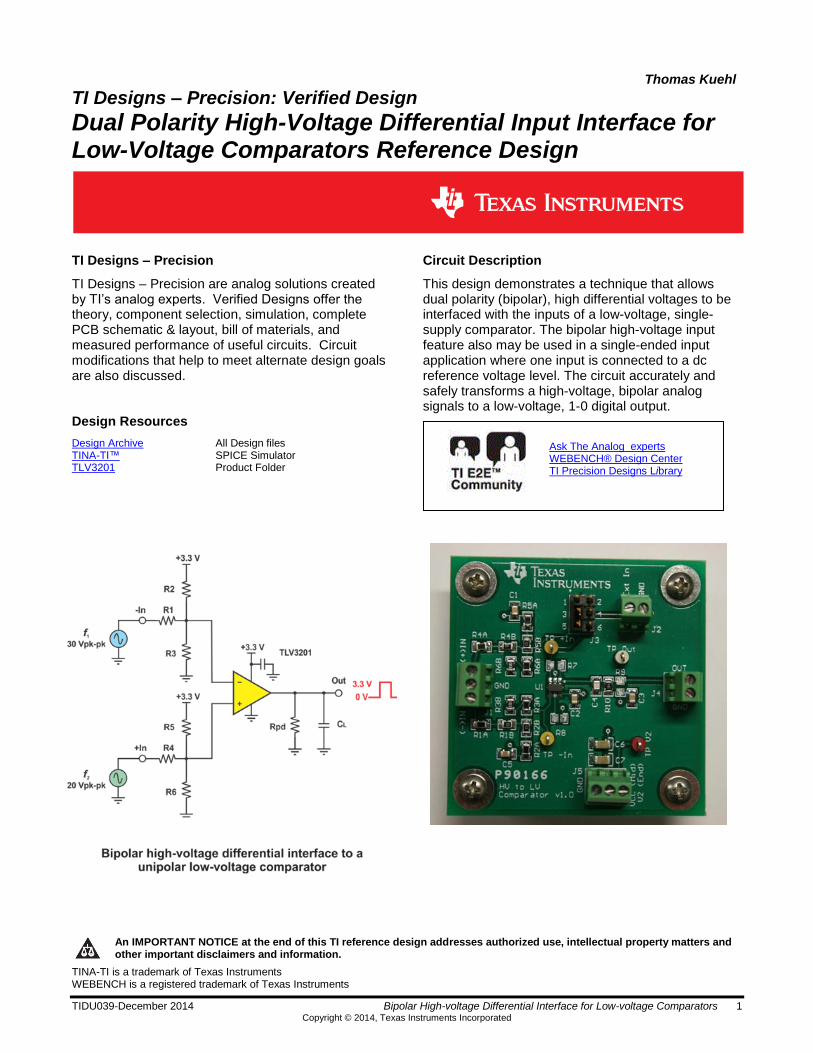
This design demonstrates a technique that allows dual polarity (bipolar), high differential voltages to be interfaced with the inputs of a low-voltage, single-supply comparator. The bipolar high-voltage input feature also may be used in a single-ended input application where one input is connected to a dc reference voltage level. The circuit accurately and safely transforms a high-voltage, bipolar analog signals to a low-voltage, 1-0 digital output.
Design Resources
Design Archive All Design files TINA-TI™ SPICE Simulator TLV3201 Product Folder
Ask The Analog experts WEBENCH® Design Center TI Precision Designs Library
www.ti.com
2 Bipolar High-voltage Differential Interface for Low-voltage Comparators TIDU039-December 2014 Copyright © 2014, Texas Instruments Incorporated
1 Design Summary The design requirements are as follows:
Supply Voltage: 3.3 V
Circuit input levels: ±15 VPK ac wave forms , 100 and 300 Hz triangle waves
Comparator input levels : 0 to 2.48 V, centered on 1.24 Vdc
Comparator common-mode range not to be exceeded
Comparator output: VOL ≤ 200 mV, and VOH ≥ 3.1 V
Use standard 0.1 % resistors in single values, or in combination
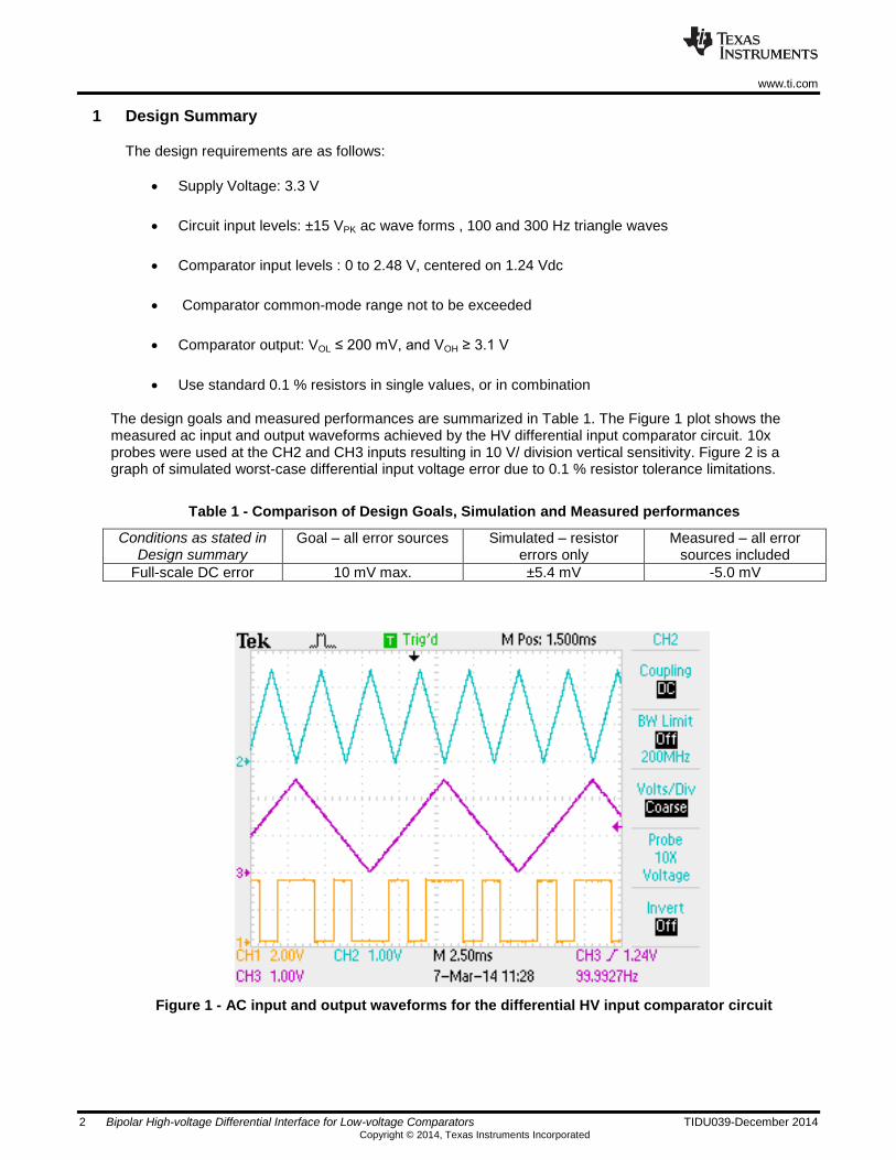
The design goals and measured performances are summarized in Table 1. The Figure 1 plot shows the measured ac input and output waveforms achieved by the HV differential input comparator circuit. 10x probes were used at the CH2 and CH3 inputs resulting in 10 V/ division vertical sensitivity. Figure 2 is a graph of simulated worst-case differential input voltage error due to 0.1 % resistor tolerance limitations.
Table 1 - Comparison of Design Goals, Simulation and Measured performances
Conditions as stated in Design summary
Goal – all error sources Simulated – resistor errors only
Measured – all error sources included
Full-scale DC error 10 mV max. ±5.4 mV -5.0 mV
Figure 1 - AC input and output waveforms for the differential HV input comparator circuit

www.ti.com
TIDU039-December 2014 Bipolar High-voltage Differential Interface for Low-voltage Comparators 3 Copyright © 2014, Texas Instruments Incorporated
Figure 2 - All combinations results for 0.1 % tolerance resistors
2 Theory of Operation
A comparator is an analog circuit that compares two voltage levels applied to its inputs and produces a high (1), or low (0) level, based on a comparison of the two voltages. The voltages being compared often have a positive polarity that is referenced to 0V, which is often ground. This input limitation is dictated by the single, positive supply commonly used. High voltage levels can be applied and compared providing the voltage is reduced by some means to a safe input level. Input voltage levels below 0 V and higher than the specified positive maximum level may fall outside the input operating input range.
Comparators can be powered by dual (+/-) power supplies allowing input voltages having either a positive, negative, or different polarities, to be compared. Powering an analog integrated circuit from dual supplies is less common than it once was because of today’s use of batteries and portable supplies. If a circuit could be devised allowing a comparator having a single supply, to be interfaced a high voltage of either polarity, many new and different comparator applications could be satisfied.
Thought was given to that idea. It was determined that a modified voltage divider could be used to not only divide down a high voltage down to a level compatible with a comparator, but also add a dc offset to keep the applied input voltage within the input the comparator’s safe input range, i.e. 0 to 3.3 V, 0 to 5 V, etc. The idea was to utilize a standard, two resistor voltage divider and sum in an offset voltage using a third resistor. The outcome is a 3-resistor network consisting of R1 – R3, or R4 – R6 as seen in the schematic on page 1.
-0.00400
-0.00300
-0.00200
-0.00100
0.00000
0.00100
0.00200
0.00300
0.00400
0 8 16 24 32 40 48 56 64
Vo
ltag
e e
rro
r (V
)
Resistor combination no.
Differential voltage error for two, 3-resistor networks
www.ti.com
4 Bipolar High-voltage Differential Interface for Low-voltage Comparators TIDU039-December 2014 Copyright © 2014, Texas Instruments Incorporated
Modern comparators, especially those using CMOS technology, are intended to use a single-polarity, low-voltage power supply. The supply may range from about 1.8 V, to 6 Vdc. The input voltage range often extends from 0 V, or even a few hundred millivolts below 0 V, to a positive voltage equal to, or even a few hundred millivolts above V+, i.e. on the order of (V-) – 100 mV to (V+) + 100 mV. The output voltage swings from a level close to the 0 V on the low end, to the V+ supply rail on the high end. The voltage swing depends on the comparator’s output stage ability to sink (open-drain) and/or source (push-pull).
Sometimes, in practical comparator applications it may be necessary compare two voltages that are outside the maximum input range of most comparators. This could include voltage levels that fall below 0 V, meaning they have a negative polarity. Satisfying these requirements and achieving adequate precision requires an input network that correctly scales the input voltage, adds the correct amount of offset, and is precise. It must accomplish these tasks while assuring the comparator’s input voltage remains within its positive, common-mode input voltage range.
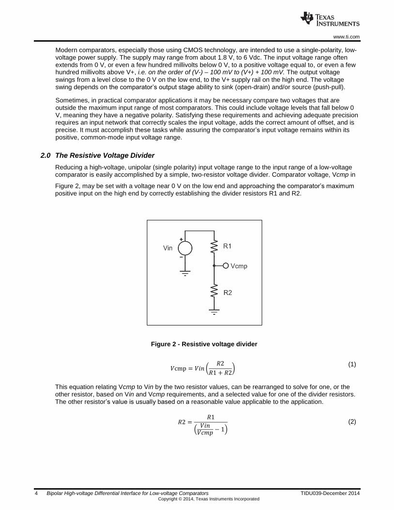
2.0 The Resistive Voltage Divider
Reducing a high-voltage, unipolar (single polarity) input voltage range to the input range of a low-voltage comparator is easily accomplished by a simple, two-resistor voltage divider. Comparator voltage, Vcmp in
Figure 2, may be set with a voltage near 0 V on the low end and approaching the comparator’s maximum positive input on the high end by correctly establishing the divider resistors R1 and R2.
Figure 2 - Resistive voltage divider
𝑉cmp = 𝑉𝑖𝑛 (𝑅2
𝑅1 + 𝑅2)
(1)
This equation relating Vcmp to Vin by the two resistor values, can be rearranged to solve for one, or the other resistor, based on Vin and Vcmp requirements, and a selected value for one of the divider resistors. The other resistor’s value is usually based on a reasonable value applicable to the application.
𝑅2 =
𝑅1
(𝑉𝑖𝑛
𝑉𝑐𝑚𝑝− 1)
(2)
www.ti.com
TIDU039-December 2014 Bipolar High-voltage Differential Interface for Low-voltage Comparators 5 Copyright © 2014, Texas Instruments Incorporated
Let’s say for example an application requires that a comparator with a maximum +3 V input must accommodate a +10 V peak input voltage from a sensor. Setting R1 equal to 100 k and applying Eq. 2, R2 is easily determined:
𝑅2 = 100 𝑘
(10
3.0−1)
= 42.7 kΩ (3)
= 42.86 kΩ
A 42.7 kΩ (0.1 %) resistance is the closest standard value. The accuracy of the voltage at the divider output is directly related to the accuracy of the applied voltage Vin and the two resistances. Limited resistor tolerance contributes error to the divider voltage. The inaccuracy of voltage Vcmp when applied to a comparator input will be seen as an error in the reference voltage level. Since the applied voltage in a comparator application is usually specified, or has an expected range, the accuracy of the comparator’s input voltage Vcmp is mostly dependent on the two divider resistances. Note that the output of the 2-resistor voltage divider cannot achieve a true 0 V level unless R2 is 0 Ohms, which negates the divider’s functionality.
2.1 Accommodating a dual polarity (bipolar), high-voltage input voltage
The two-resistor voltage divider provides a straightforward means to reduce a high-voltage before it is applied to the comparator input. However, there may be a need to compare levels that are very close to zero volts, or even having a negative polarity. Ac voltages can swing well above and below zero volts in the positive and negative portions of its cycle. Most comparators cannot accommodate a negative input range when powered by the single polarity, positive supply most commonly applied in analog circuits.
Intuitively, one might conclude that with the right amount of offset injected into the voltage divider, that not only positive voltages, but negative voltages too could be accommodated. Then, the voltage from the divider applied to the comparator input would be 0 V or a positive level only. This is true providing that a) the added offset is sufficiently positive enough to keep the comparator input from being driven below its specified minimum level (presumably a level near 0 V), and b) the added offset is not so high and positive such that it overdrives the comparator’s input beyond its maximum positive input level. An added requirement is the divider should be precise so that the comparator’s input voltage, Vcmp, is also precise.
These goals can be achieved with a 3-resistor input network. It is a remarkably simple solution providing it is understood that the simple circuit has some minor limitations. Nonetheless, the proposed use of a 3-resistor input network satisfies most application needs where a high-voltage, possibly dual input polarity analog level comparison is required.
2.2 3-resistor input network The proposed 3-resistor input network is shown is figure 4. Resistor R1 will be referred to as the input resistor, R2 the upper voltage divider resistor, and R3 the lower voltage divider resistor. All three of these resistors work together to; a) divide the high-voltage input range to one compatible with the comparator input range, b) establish a precise input reference and c) and be set up in a manner as to keep the input voltage from exceeding the comparator’s input common-mode operating range.

www.ti.com
6 Bipolar High-voltage Differential Interface for Low-voltage Comparators TIDU039-December 2014 Copyright © 2014, Texas Instruments Incorporated
Figure 3 - The 3-resistor network
The voltage Vin represents the bipolar, high-voltage input coming from the input source. Vref is a voltage source that provides a source of current to divider resistors R2 and R3. Vcmp is the voltage that is developed at the output of the network and is applied to a comparator input. The voltage divider behavior is now more involved than in the two-resistor case because of the addition of R1. In addition, the voltage level established at Vcmp is now a function of voltages Vin and Vref as well. The extent of Vin’s influence on Vcmp is controlled by the magnitude and polarity of Vin and the resulting current through R1. The 3 resistors must be correctly established to satisfy the three conditions previously stated.
Redrawing the 3-resistor network as seen in Figure 5 can be useful for analyzing the circuit.
Figure 4 - The 3-resistor network rearranged for Superposition analysis
Using Superposition the following equation was derived for the comparator input voltage, Vcmp:
𝑉cmp = 𝑉𝑖𝑛 [
(𝑅2 ∙ 𝑅3)𝑅2 + 𝑅3
𝑅1 +(𝑅2 ∙ 𝑅3)𝑅2 + 𝑅3
] + 𝑉𝑟𝑒𝑓 [
(𝑅1 ∙ 𝑅3)𝑅1 + 𝑅3
𝑅2 +(𝑅1 ∙ 𝑅3)𝑅1 + 𝑅3
]
(4)
This was simplified with the aid of Mathcad to:
𝑉cmp =𝑉𝑟𝑒𝑓(𝑅1 ∙ 𝑅3) + 𝑉𝑖𝑛(𝑅2 ∙ 𝑅3)
(𝑅1 ∙ 𝑅2) + (𝑅1 ∙ 𝑅3) + (𝑅2 ∙ 𝑅3)
(5)

www.ti.com
TIDU039-December 2014 Bipolar High-voltage Differential Interface for Low-voltage Comparators 7 Copyright © 2014, Texas Instruments Incorporated
Thus, a relationship for Vcmp, the voltage at the comparator input is established based on the Vin, Vref, selections and the three network resistors R1, R2 and R3. The 3 voltage levels are set based on the specific application requirements.
There is a degree of freedom in that one of the three resistor values may be freely selected based upon a practical, precision value. R2 is selected as that resistor in the remaining derivations. Then, R1 and R3 are derived based on the selected R2 value and the 3 voltages.
R1 can be determined rather easily with the aid of figure 6. The circuit condition is with Vin set to the most negative intended input level, which corresponds to Vcmp being 0 V.
Figure 6 – Deriving R1 based on the current through R2
When Vcmp is 0V it is at the same potential as ground meaning no current flows through R3. Any current sourced by Vref will only flow through R2 and R1 as illustrated in the figure 6, left-hand circuit. R3 can be removed from the circuit for analysis purposes and the equivalent circuit is shown in the right-hand circuit. Then, R1 is determined by the voltage developed across it, and the current through it, established by Vref and selected R2 value.
𝑅1 = 𝑉𝑖𝑛
𝐼1=
𝑉𝑖𝑛
(𝑉𝑟𝑒𝑓
𝑅2)
(6)
Now that equations for R1 and R2 are established, equation 5 can be rearranged to solve for R3:
𝑅3 =𝑉𝑐𝑚𝑝(𝑅1 ∙ 𝑅2)
(𝑉𝑟𝑒𝑓 ∙ 𝑅1) + (𝑉𝑖𝑛 ∙ 𝑅2) − (Vcmp ∙ 𝑅1) − (Vcmp ∙ R2)
(7)
These equations are simple enough that they can be solved using a spreadsheet, or hand calculator.
2.3 Calculating the 3-resistor network resistor values
A procedure is provided here to guide in the determination of the three resistor values:
1. Select a resistance value for resistor R2. Typically, this will be tens-of-kilohms but may be higher, or
lower, depending on the application.

www.ti.com
8 Bipolar High-voltage Differential Interface for Low-voltage Comparators TIDU039-December 2014 Copyright © 2014, Texas Instruments Incorporated
2. Decide on the Vref voltage level. This voltage biases the 3-resistor network. It can be the supply voltage
used to power the comparator in low accuracy applications; however, a precise reference voltage will
likely be required for high accuracy applications.
3. Now let Vcmp be equal to the low-end of the comparator input range. The R1 math solution is based on 0
V, and is common for modern rail-to-rail input comparators.
4. Use equation 6 to calculate R1. Its value is based upon the most negative Vin input voltage that will be
applied at the R1 network input connection. This voltage level drives Vcmp to its minimum input level 0 V.
5. Now set Vin equal to 0 V.
6. Calculate R3 using equation 7. Vcmp should be set to equal the midscale voltage of the comparator’s
planned input voltage range. The voltage input voltage swing is symmetrical about this Vcmp level. Select
Vcmp to keep the input voltage within the comparator’s safe input range. For example, if the comparator
has an input range is 0 to 3 V then Vcmp would be 1.5 V.
Here is an example of this procedure based on the conditions stated in the Section 1, Design Summary:
Supply Voltage: 3.3 V – this is the voltage level that will be used for Vref
Circuit input levels: ±15 VPK ac wave forms , 100 and 300 Hz triangle waves
Comparator input levels : 0 to 2.48 V, centered on 1.24 Vdc. The 2.48 V maximum input level was
simply and arbitrarily selected for this example. A voltage up to a maximum positive, input
common-mode voltage could have been used.
1. Select a value for R2. For this example, a resistance of 49.9 kΩ is used. It is a common, practical value
available with low and precise tolerance from ±0.1 % to ±1 %.
2. Set the Vref level to 3.3 V. The same as the comparator V+ supply voltage in this case.
3. Set Vcmp to 0 V.
4. Set Vin to the most negative level, -15 V. Use the absolute value, 15 V.
5. Calculate R1 from equation 6:
𝑅1 = 𝑉𝑖𝑛
𝐼1=
𝑉𝑖𝑛
(𝑉𝑟𝑒𝑓
𝑅2)
(6)
R1 =15 𝑉
(3.3 𝑉
49.9 𝑘Ω)
= 226.8 𝑘Ω (8)
6. Now set Vin to 0 V. Calculate the R3 resistance using equation 7. Remember Vcmp is specified to be
1.240 V:
www.ti.com
TIDU039-December 2014 Bipolar High-voltage Differential Interface for Low-voltage Comparators 9 Copyright © 2014, Texas Instruments Incorporated
𝑅3 =𝑉𝑐𝑚𝑝(𝑅1 ∙ 𝑅2)
(𝑉𝑟𝑒𝑓 ∙ 𝑅1) + (𝑉𝑖𝑛 ∙ 𝑅2) − (Vcmp ∙ 𝑅1) − (Vcmp ∙ R2)
(9)
𝑅3 =1.24(226.82 ∙ 103 ∙ 49.9 ∙ 103)
(3.3 ∙ 226.82 ∙ 103) + (0 ∙ 49.9 ∙ 103) − (1.24 ∙ 226.82 ∙ 103) − (1.24 ∙ 49.9 ∙ 103)
(10)
R3 = 34.62 kΩ
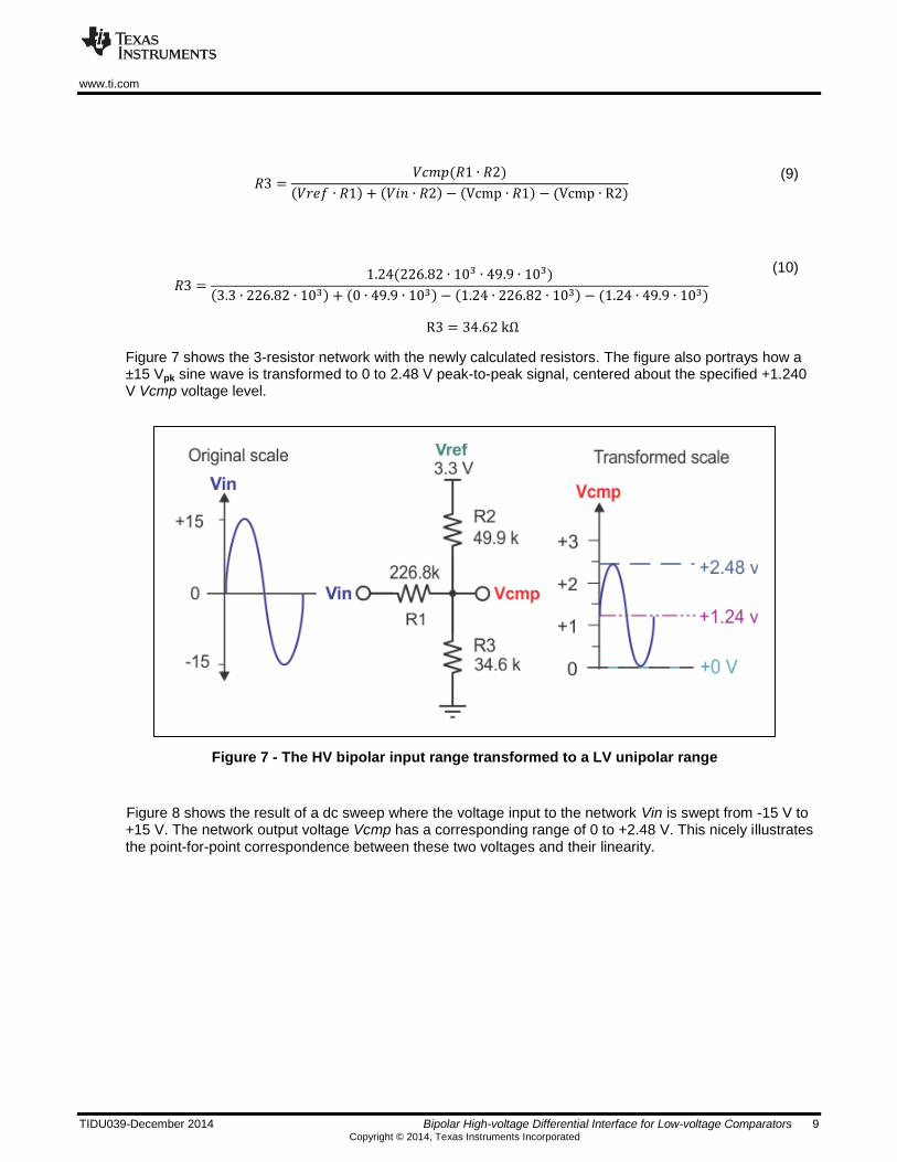
Figure 7 shows the 3-resistor network with the newly calculated resistors. The figure also portrays how a ±15 Vpk sine wave is transformed to 0 to 2.48 V peak-to-peak signal, centered about the specified +1.240 V Vcmp voltage level.
Figure 7 - The HV bipolar input range transformed to a LV unipolar range
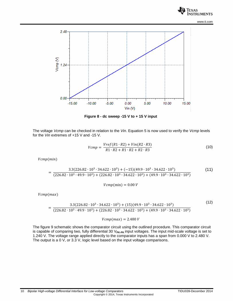
Figure 8 shows the result of a dc sweep where the voltage input to the network Vin is swept from -15 V to +15 V. The network output voltage Vcmp has a corresponding range of 0 to +2.48 V. This nicely illustrates the point-for-point correspondence between these two voltages and their linearity.
www.ti.com
10 Bipolar High-voltage Differential Interface for Low-voltage Comparators TIDU039-December 2014 Copyright © 2014, Texas Instruments Incorporated
Figure 8 - dc sweep -15 V to + 15 V input
The voltage Vcmp can be checked in relation to the Vin. Equation 5 is now used to verify the Vcmp levels for the Vin extremes of +15 V and -15 V.
𝑉𝑐𝑚𝑝 = 𝑉𝑟𝑒𝑓(𝑅1 ∙ 𝑅2) + 𝑉𝑖𝑛(𝑅2 ∙ 𝑅3)
𝑅1 ∙ 𝑅2 + 𝑅1 ∙ 𝑅2 + 𝑅2 ∙ 𝑅3 (10)
𝑉𝑐𝑚𝑝(𝑚𝑖𝑛)
= 3.3(226.82 ∙ 103 ∙ 34.622 ∙ 103) + (−15)(49.9 ∙ 103 ∙ 34.622 ∙ 103)
(226.82 ∙ 103 ∙ 49.9 ∙ 103) + (226.82 ∙ 103 ∙ 34.622 ∙ 103) + (49.9 ∙ 103 ∙ 34.622 ∙ 103)
(11)
𝑉𝑐𝑚𝑝(min) = 0.00 𝑉
𝑉𝑐𝑚𝑝(𝑚𝑎𝑥)
= 3.3(226.82 ∙ 103 ∙ 34.622 ∙ 103) + (15)(49.9 ∙ 103 ∙ 34.622 ∙ 103)
(226.82 ∙ 103 ∙ 49.9 ∙ 103) + (226.82 ∙ 103 ∙ 34.622 ∙ 103) + (49.9 ∙ 103 ∙ 34.622 ∙ 103)
(12)
𝑉𝑐𝑚𝑝(𝑚𝑎𝑥) = 2.480 𝑉
The figure 9 schematic shows the comparator circuit using the outlined procedure. This comparator circuit is capable of comparing two, fully differential 30 VPK-PK input voltages. The input mid-scale voltage is set to 1.240 V. The voltage range applied directly to the comparator inputs has a span from 0.000 V to 2.480 V. The output is a 0 V, or 3.3 V, logic level based on the input voltage comparisons.

www.ti.com
TIDU039-December 2014 Bipolar High-voltage Differential Interface for Low-voltage Comparators 11 Copyright © 2014, Texas Instruments Incorporated
Figure 9 - Fully differential, dual-polarity HV input to LV input comparator circuit
The 3-resistor network is an attenuator in one of its roles and an offset generator in the other. Its gain is very much less than 1 V/V when accommodating input voltages of tens, or hundreds, of volts. Using the above example where the input voltages were ±15 V and output voltages from the 3-resistor network of 2.480 V and 0.0 V, the voltage gain (or attenuation) can be determined:
Av =𝛥𝑉𝑐𝑚𝑝
ΔVin
(13)
Calculating the attenuation for the example 3-resistor network from equation 9:
𝐴𝑣 =2.480 − (0)
15 − (−15)= 82.7 ∙ 10−3V/V (14)
Converting to dB:
𝐴𝑣(𝑑𝐵) = 20 ∙ log Av (15)
Av(dB) = 20 ∙ log 82.710−3 = −21.6 dB (16)
The numbers indicate that the network’s output voltage Vcmp is less than 1/100
th of the input voltage Vin.
This has two implications for voltages applied to the input:
This 3-resistor network circuit approach is primarily intended for comparing large voltages against
one another. If an input voltage is very small, it might be comparable in level with the noise and the
comparator will not react to it.
Conversely, noise and small dc and ac error voltages appearing at the network input is much
reduced by the network’s attenuation factor.
www.ti.com
12 Bipolar High-voltage Differential Interface for Low-voltage Comparators TIDU039-December 2014 Copyright © 2014, Texas Instruments Incorporated
3 Component Selection
The selection of the comparator and resistors and their associated critical characteristics are discussed fully in the following subsections.
3.1 Error Analysis
Ideally, the comparator will be perfect with both inputs having perfectly matched responses, the resistors would be their exact in value and the voltage applied to the 3-resistor perfect too. Realistically, that won’t be the case and there are limits to how close to ideal things will be. If care is taken, the errors can be minimized and good, precise comparator action can be delivered from the circuit.
3.2 The Comparator Errors
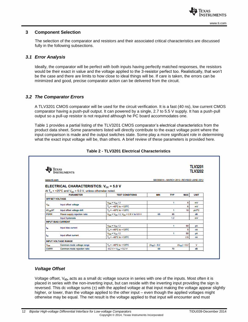
A TLV3201 CMOS comparator will be used for the circuit verification. It is a fast (40 ns), low current CMOS comparator having a push-pull output. It can powered by a single, 2.7 to 5.5 V supply. It has a push-pull output so a pull-up resistor is not required although he PC board accommodates one. Table 1 provides a partial listing of the TLV3201 CMOS comparator’s electrical characteristics from the product data sheet. Some parameters listed will directly contribute to the exact voltage point where the input comparison is made and the output switches state. Some play a more significant role in determining what the exact input voltage will be, than others. A brief review of these parameters is provided here.
Table 2 - TLV3201 Electrical Characteristics
Voltage Offset
Voltage offset, VIO, acts as a small dc voltage source in series with one of the inputs. Most often it is placed in series with the non-inverting input, but can reside with the inverting input providing the sign is reversed. This dc voltage sums (±) with the applied voltage at that input making the voltage appear slightly higher, or lower, than the voltage applied to the other input – even though the applied voltages might otherwise may be equal. The net result is the voltage applied to that input will encounter and must
www.ti.com
TIDU039-December 2014 Bipolar High-voltage Differential Interface for Low-voltage Comparators 13 Copyright © 2014, Texas Instruments Incorporated
overcome the offset in order for the comparator to switch output states. The TLV3201 can have a VIO as much as ±5 mV (25°C), but more often it will be closer to the ±1 mV level listed as “TYP” (typical).
Voltage Offset Drift The voltage offset VIO parameter is temperature sensitive and will likely change when the comparator is exposed to temperature change. This input offset temperature dependency (dVos/dT) is called voltage offset drift, or simply “drift.” The TLV3201 has a maximum limit of 10 uV/°C, and a typical value of 1 uV/°C. Drift can be positive, negative, or even zero in different regions of the operating temperature range. A device subjected to a +100°C temperature change and having a drift of -1 uV/°C over that range would subtract 100 uV from the 25°C room temperature VIO. Conversely, a device having a +1 uV/°C drift would exhibit a +100 uV increase in VIO for the same +100°C temperature change.
Power Supply Rejection Power supply rejection ratio, PSRR, is a measure of the comparator’s ability to reject, or ignore, a change in VIO as the power supply voltage changes. The TLV3201 has a typical PSRR of 85 dB, when the supply, Vcc, is changed from 2.5 V, to 5.5V (Δ3 V delta). Equated in terms of a V/V unit measure, 85 dB is equal to:
𝑉𝐼𝑂−𝑃𝑆𝑅𝑅 =10−(
𝑃𝑆𝑅𝑅20 𝑑𝐵
)
∆V +
(17)
VIO−PSRR = 10
−8520
3=
56 uV
3 V= 18.7 uV/V (18)
The sign for VIO may be positive, or negative, depending on the common-mode voltage (VCM) level and the polarity of the power supply change. This error voltage will sum with VIO as did the drift. Do note that the PSRR has a minus sign associated with it because the resulting change in VIO is much smaller than the intentional change in supply voltage i.e. the common-mode gain is much, much less than 1V/V.
Input Bias Current
Another error source that contributes to the total voltage offset is the input bias current IB, that flows through the resistor input network. This TLV3201 Ib is listed with a 1 pA typical, and 50 pA maximum, at 25°C. However, it can be as high as 5 nA, over the -40°C to +125°C temperature range. It’s highest IB occurs at the highest operating temperature. The input IB of the TLV3201, a CMOS comparator, is comprised of a small amount of gate current and a much larger leakage current related to the input ESD protection cell. Leakage current approximately doubles with each +10°C increase in temperature. By time 125°C is reached IB will be orders of magnitude higher than the 25°C level.
If IB is small at room temperature, say 5 pA, and it flows through an equivalent input network resistance of 100 kΩ, the voltage drop is about 0.5 uV - quite small. However, if the temperature is increased to 125°C, the IB will increase to around 5 pA. Using the same 100 kΩ equivalent resistance the voltage offset contribution increases to 500 uV.
Since the two inputs are not perfectly matched there will be a small difference in their individual IB levels. This difference is called input current offset, IIO. The TLV3201 current offset IIO, is comparable in magnitude to the input IB. If, for example, one input has an IB of +5 pA and the other +3 pA, the IIO would be 2 pA. If each of these current flow through an equivalent network resistance of 100 kΩ, the voltage offset would be:
VIO−IIO = 𝐼𝐵1 ∙ 𝑅𝐸𝑄 − 𝐼𝐵2 ∙ 𝑅𝐸𝑄 (19)
𝑉𝐼𝑂−𝐼𝐼𝑂 = (5 ∙ 10−12𝑥 1 ∙ 105) − (3 ∙ 10−12𝑥 1 ∙ 105) = 200 𝑛𝑉
(20)

www.ti.com
14 Bipolar High-voltage Differential Interface for Low-voltage Comparators TIDU039-December 2014 Copyright © 2014, Texas Instruments Incorporated
At an elevated temperature of 125°C, the first input’s IB increases to 5.2 pA, while the other’s increases to 3.1 pA through the 100 kΩ resistance are 520 uV and 310 uV, respectively. The IB drift contribution to VIO is their difference:
𝑉𝐼𝑂−𝐼𝐼𝑂 = 520 𝑢𝑉 − 310 𝑢𝑉 = 210 𝑢𝑉
(21)
Room temperature IB may not add much to the offset, but its contribution can be significant at elevated hot temperatures where it can be significantly higher for CMOS and JFET input comparators.
Common-mode Rejection Ratio
The VIO component of the total offset is most often specified with the comparator inputs at a particular input voltage level. This input level is referred to as the common-mode voltage level, VCM. Even though the TLV3201 has a VCM range extending from (VEE - 0.2 V) to (VCC + 0.2 V), VIO is specified with it set to VCC/2, or mid-scale which is quite common. This is +2.5 V for a +5 V supply application. VIO will likely change from its mid-scale value as VCM is moved through its specified range.
The common-mode rejection ratio (CMRR) specification provides a measure of how VIO changes as the result of a change in VCM. CMRR is defined by:
CMRR (dB) = 20log |∆VCM
∆VIO
| (22)
The TLV3201 minimum CMRR is listed as 60 dB. To get an idea how much of a change VIO may undergo as VCM is changed the CMRR equation is rearranged. A minus sign is added to the CMRR number because the net change in VIO is much less than the change in VCM:
VIO−CMRR = 10
−CMRR(dB)
20dB∆VCM
(23)
The ΔVCM change can be between any two voltage levels within the VCM input range, but most often it is relative to the mid-scale voltage. It is convenient to use a 1 V/V change which relative to a 2.5 V mid-scale voltage with the other VCM voltage being 1.5 V, or 3.5 V. Applying the 60 dB CMRR:
VIO−CMRR = 10
−60 dB20 dB
(3.5 V−2.5 V)
VIO−CMRR = 1 mV
(24
A 1 V change in VCM has results in a 1 mV change in VIO which is a fairly large change. The typical TLV3201 CMRR is 70 dB which equates to a common-mode voltage sensitivity of 316 uV/V.
Combined Comparator Errors (Root Sum Squared)
Analog electronic parameters most often have a Normal Distribution, with the typical values being commonly attained. Because of this each of the errors can be combined by applying the Root Sum Square. Each offset contribution is combined at the comparator’s non-inverting input, as illustrated in Figure 10. The VIO contributions from those parameters sensitive to a temperature change, such as supply voltage and common-mode voltage, would actually require a change in temperature for them to be a contributor.

www.ti.com
TIDU039-December 2014 Bipolar High-voltage Differential Interface for Low-voltage Comparators 15 Copyright © 2014, Texas Instruments Incorporated
Figure 10 - all sources that contribute to voltage offset
The signs were arbitrarily assigned in the figure and the contribution from each source is indicated. The total voltage offset, VIO_total, is determined as a root sum square (RSS) value made up of all the VIO contributors. It is equivalent to:
VIO_total(RSS) = [VIO
2 + (dVIO
dT)2 + (VIO−PSRR)2 + (VIO−Ib)2 + (VIO−IIO)2
+ (VIO−CMRR)2]1/2
(25)
We’ll pretend for now that the mentioned temperature change, voltage change, etc., all occurred. Then, VIO_total (RSS) is calculated:
VIO_total(RSS) = [(1 ∙ 10−3)2 + (−1 ∙ 10−4)2 + (18.7 ∙ 10−6)2 + (1 ∙ 10−5)2 + (1 ∙ 10−5)2
+ (1 ∙ 10−3)2]1/2 (26)
VIO_total(RSS) = 1.42 ∙ 10−3V, or 1.42 mV
When the magnitude of each source making up the voltage offset are considered the initial VIO and VIO-
CMRR are the most significant contributors. Unless the circuit is to be operated at elevated temperature where VIO-Ib can become large it may only be necessary to consider these two parameters. Doing so in this case results in a VIO_total (RSS) of 1.41 mV. For more information about Root Sum Squares analysis, see the TI Precision Designs Hub blog, “Will the real Vos please stand up,” referenced in Section 11.
4 Simulation
The comparator circuit established in figure 9 was entered into the TINA-TI using its circuit simulation schematic capture capability. A TLV3201 low-voltage, CMOS comparator was chose to validate the circuit’s performance. The TLV3201 has a modern PSpice-based simulation model and reference circuit. They are available from the TI TLV3201 product web page: http://www.ti.com/product/tlv3201 Look under the tab Tools & Software > Models DC and ac simulations to assure the circuit’s performances met expectations were conducted. The circuit in figure 11 is nearly identical to that in figure 9, except dc input voltage sources are used and voltmeters are added at the comparator inputs and the output. A dc simulation was made first to make certain that the

www.ti.com
16 Bipolar High-voltage Differential Interface for Low-voltage Comparators TIDU039-December 2014 Copyright © 2014, Texas Instruments Incorporated
circuit is operating as expected. It is always a best practice to run a dc simulation first to confirm that things look correct before running an ac, or transient, analysis. The dc simulation result indicates the voltmeter levels and the comparator supply current. The comparator’s (-) inverting input voltage is about -100 uV, with -15 V applied to the 3-resistor network input. The expected +1.24 V level is present at the comparator (+) non-inverting input, with 0 V applied to its 3-resistor network input. Because the comparator’s non-inverting input is at +1.24 V and the inverting input is at about 0 V, the comparator output is in the high output state at 3.29 V. The TLV3201’s push-pull output stage easily sources enough current through the 10 kΩ load resistor such that the output pulls up very close to the +3.3 V supply level.
Figure 11 - TINA dc simulation circuit
Figure 12 shows the first ac simulation circuit. It is very similar to the dc circuit, except the dc source associated with the inverting input has been replaced with an ac waveform generator. Again, the input networks were designed to establish +1.240 V dc at each comparator input when the input source voltage is set to 0 V. A ±15 VPK, 300 Hz saw-tooth wave generated by source VS1 is applied to Vin-. The Vin- and Vo waveforms are seen in Figure 13. This diagram is the output from a TINA-TI transient analysis. Observe how the TLV3201 output changes state each time the triangle wave’s level passes through the 1.24 V dc reference level seen as the Vcmp- midpoint. If this reference voltage is changed, the point at which the comparison is accomplished will move with it.

www.ti.com
TIDU039-December 2014 Bipolar High-voltage Differential Interface for Low-voltage Comparators 17 Copyright © 2014, Texas Instruments Incorporated
Figure 12 - TINA ac simulation circuit with Vcmp- driven by a saw-tooth, Vcmp+ at 1.24 V dc level
Figure 13 - TINA transient simulation for Vcmp- driven by saw-tooth, Vcmp+ at 1.24 V dc level
www.ti.com
18 Bipolar High-voltage Differential Interface for Low-voltage Comparators TIDU039-December 2014 Copyright © 2014, Texas Instruments Incorporated
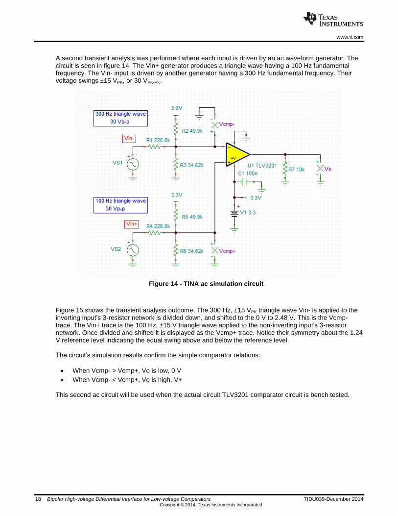
A second transient analysis was performed where each input is driven by an ac waveform generator. The circuit is seen in figure 14. The Vin+ generator produces a triangle wave having a 100 Hz fundamental frequency. The Vin- input is driven by another generator having a 300 Hz fundamental frequency. Their voltage swings ±15 VPK, or 30 VPK-PK.
Figure 14 - TINA ac simulation circuit
Figure 15 shows the transient analysis outcome. The 300 Hz, ±15 VPK triangle wave Vin- is applied to the inverting input’s 3-resistor network is divided down, and shifted to the 0 V to 2.48 V. This is the Vcmp- trace. The Vin+ trace is the 100 Hz, ±15 V triangle wave applied to the non-inverting input’s 3-resistor network. Once divided and shifted it is displayed as the Vcmp+ trace. Notice their symmetry about the 1.24 V reference level indicating the equal swing above and below the reference level.
The circuit’s simulation results confirm the simple comparator relations:
When Vcmp- > Vcmp+, Vo is low, 0 V
When Vcmp- < Vcmp+, Vo is high, V+
This second ac circuit will be used when the actual circuit TLV3201 comparator circuit is bench tested.

www.ti.com
TIDU039-December 2014 Bipolar High-voltage Differential Interface for Low-voltage Comparators 19 Copyright © 2014, Texas Instruments Incorporated
Figure 15 - TINA transient simulation Vcmp- and Vcmp+ driven by triangle waves
5 Network Resistance Errors
The inaccuracy of the input 3-resistor network is a primary error source that affects the comparator input voltage. Even though they have ideal, calculated values, real resistors come in fixed values that vary within their rated tolerance range. If nearly exact resistances are required standard value, low tolerance resistors can be combined in series, or parallel, to reduce the resistance value error. Today, low tolerance 0.1 % tolerance resistors are readily available at reasonable prices and offered in modern, surface-mount packaging. Tolerances of 0.05 % and 0.025 % are obtainable and will reduce tolerance related errors. The 3-resistor networks used at the comparator inputs in this study were specified with a tolerance of 0.1 %. Looser tolerance resistors could have been used but the accuracy of Vcmp would likely suffer. R2, the 49.9 kΩ in the previous 3-resistor network example, when specified with a ±0.1 % tolerance has a resistance span of ±50 Ω. That increases to ±500 Ω with a ±1 % tolerance resistor. Since there are 3 resistors in each input network having their own variance, Vcmp can be much different than expected.

www.ti.com
20 Bipolar High-voltage Differential Interface for Low-voltage Comparators TIDU039-December 2014 Copyright © 2014, Texas Instruments Incorporated
5.2 Worst Case Resistor Tolerance Analysis
Resistors should have a resistance that falls within their rated tolerance window. And when there is a need to know how large the resistor-related Vcmp error can be, a worst-case analysis will provide that information. Precise, low tolerance resistors are often trimmed for the ideal value, but have a distribution about it. Most resistors don’t attain the worst-case values found at the ends of the tolerance window. The worst-case resistor spread and its effect on Vcmp was analyzed two ways: a) TINA Spice Worst-Case Analysis capability b) A mathematical worst-case analysis involving all six resistor maximum/minimum combinations (2
6)
Only the TINA Spice analysis is presented here; the mathematical worst-case analysis is provided in Appendix D. It is presented in an Excel spreadsheet format that accommodates user inputs. That analysis is more detailed in that it provides the worst-case error for all 64 minimum/maximum value combinations.
TINA Spice Worst Case Analysis The worst-case resistor tolerance related errors are evaluated using TINA Spice’s Worst Case Analysis capability. This analysis capability is only available with for-purchase versions of the program and not the freeware, TINA-TI version. This method relies on using the circuit simulation capabilities of the TINA Spice simulator. The end result is a histogram plot showing the occurrences of the voltage levels produced by the various resistor combinations. It provides an easy-to-view, graphical plot showing a distribution of possible Vcmp voltage levels, but more importantly the Vcmp extremes.
TINA Spice Worst Case Analysis and Histogram Procedure The procedure described is a step-by-step produce that produces a histogram based upon combinations of worst case values for the 3 resistors. Anyone moderately familiar with using TINA Spice will be able to understand and follow each step. Other Pspice-based simulators may offer a similar statistical analysis capability and one should check their simulator documentation if interested in performing the analysis.
Figure 16 below, shows a TINA schematic containing two 3-resistor networks, one each, for each comparator input. Both are driven by the same input source Vin, which is set initially to 15 V. The network resistances are sequentially cycled to their tolerance extremes. When the two resistor networks have the ideal resistor values the Vcmp+ and Vcmp- should be equal and 1.240 V, with the difference between them equal to 0 V. However, any deviation in the resistor values from the ideal values will cause Vcmp+ and Vcmp- to change. Their difference is a differential voltage labeled Vdiff, and is the error voltage developed between them contributed by mismatch.

www.ti.com
TIDU039-December 2014 Bipolar High-voltage Differential Interface for Low-voltage Comparators 21 Copyright © 2014, Texas Instruments Incorporated
Figure 16 - TINA circuit used for Worst Case analysis
Once the TINA Industrial version is running and the figure 16 circuit has been entered the following procedure is used to perform a Worst Case analysis: 1. Set up the resistor tolerance and distribution:
a. Double click on a resistor to open its characteristics window
b. Click on the 3 dot pattern next to the resistor value
c. When the next window opens enter the Tolerance (0.1 %, or whatever is being used) and set
the Distribution bullet to Uniform.
d. Do this for all 6 resistors in the two, 3-resistor networks
e. Close the resistor windows
2. Setting up for a Worst Case dc analysis
a. Select the Analysis Mode tab at the top of the TINA workspace
b. Set the Worst Case bullet
c. Check Analytic for Method
d. Number of cases will be automatically set to 64 (26 resistor combinations) by step 2c.
e. Click on OK
3. Select Analysis > DC Analysis > DC Transfer Characteristics
a. A DC Transfer Characteristic window opens
www.ti.com
22 Bipolar High-voltage Differential Interface for Low-voltage Comparators TIDU039-December 2014 Copyright © 2014, Texas Instruments Incorporated
b. Enter START and STOP voltages. A small + and – voltage, above and below the target
voltage is good; Vin + 100 mV, Vin - 100 mV for example.
c. Set the Number of points to 64. The same as step 2d.
d. For Input select Vin, the source being evaluated in this case to +15 V (or 0 V, +15 V, etc.)
e. Click OK and the calculations will commence
4. When the calculation period has completed a window opens showing multiple graph traces of Vin vs. a
voltage which is actually Vdiff.
a. Select the EDIT tab
b. Next, Select all curves. All of the curves will turn red at that time.
5. Running the statistics
a. Select Process > Statistics
b. The Tolerance Analysis – Statistics window opens
c. Select Output
d. Vdiff should be present in the pull down space
e. Set the Option bullet to CUT and enter Vin level in its block
f. Set the Number of bars to 20 (no. of histogram bars)
g. Click Calculate, then Draw
h. A histogram for Vdiff, (Vcmp+ - Vcmp-) is displayed
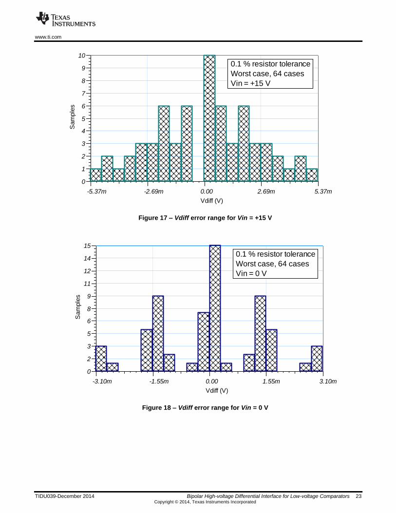
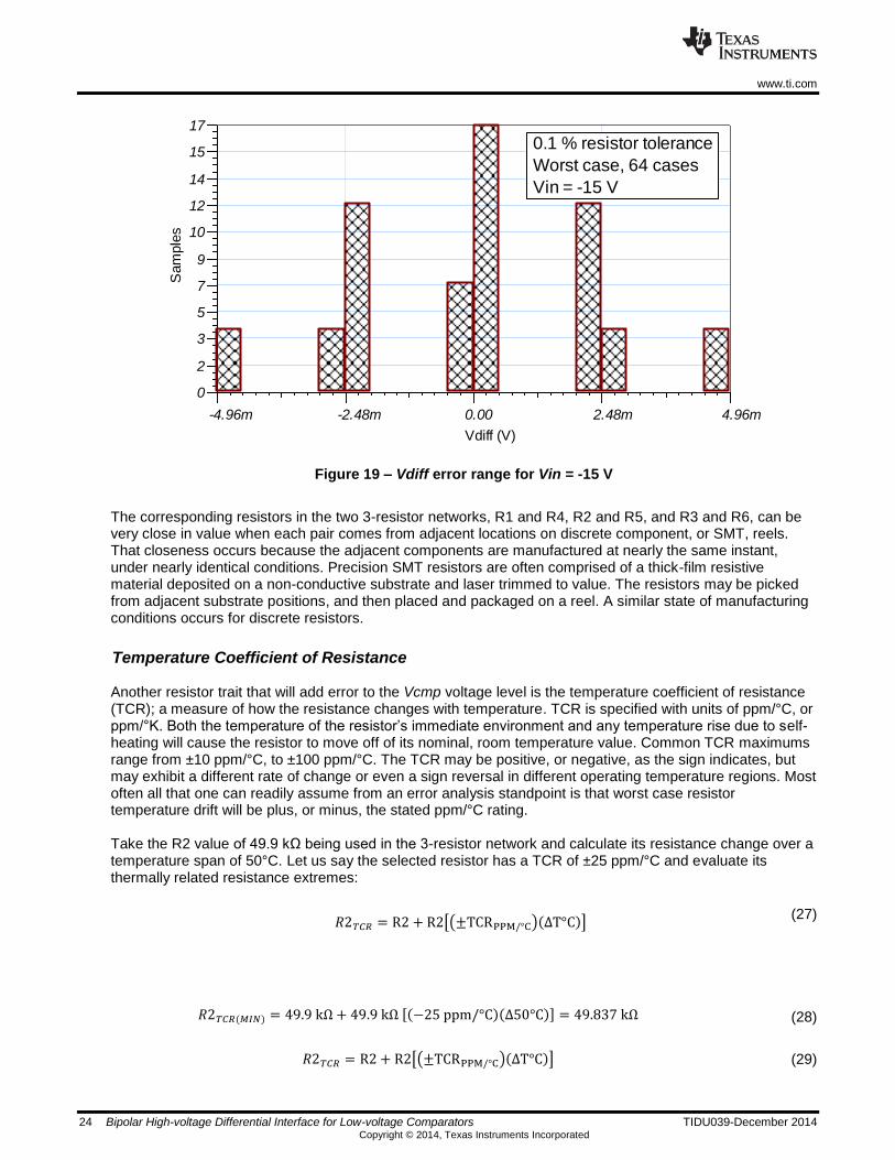
Histograms were developed with input voltages of +15 V, 0 V, and then -15 V. They are seen in figures 17 through 19. Any input level within the specified input range can be evaluated providing the statistics settings comply with the outlined procedure. Three observations about the histograms:
The maximum Vdiff error is dependent on the Vin voltage level being applied.
The Vdiff error grouping changes with Vin level.
The Vdiff error is symmetrical about 0 V. The symmetry in the center looks to be off, but it is solely
because TINA only allows a fixed number of bins, 10 , 20, etc.
Most often it will be the worst-case Vdiff error that will be of the highest importance in relation to the
application’s required accuracy. Here the maximum error is ±5.37 mV which occurs when Vin equals +15
V.
www.ti.com
TIDU039-December 2014 Bipolar High-voltage Differential Interface for Low-voltage Comparators 23 Copyright © 2014, Texas Instruments Incorporated
Figure 17 – Vdiff error range for Vin = +15 V
Figure 18 – Vdiff error range for Vin = 0 V
T
Vdiff (V)
-5.37m -2.69m 0.00 2.69m 5.37m
Sam
ple
s
0
1
2
3
4
5
6
7
8
9
10
0.1 % resistor tolerance
Worst case, 64 cases
Vin = +15 V
T
Vdiff (V)
-3.10m -1.55m 0.00 1.55m 3.10m
Sam
ple
s
0
2
3
5
6
8
9
11
12
14
15
0.1 % resistor tolerance
Worst case, 64 cases
Vin = 0 V
www.ti.com
24 Bipolar High-voltage Differential Interface for Low-voltage Comparators TIDU039-December 2014 Copyright © 2014, Texas Instruments Incorporated
Figure 19 – Vdiff error range for Vin = -15 V
The corresponding resistors in the two 3-resistor networks, R1 and R4, R2 and R5, and R3 and R6, can be very close in value when each pair comes from adjacent locations on discrete component, or SMT, reels. That closeness occurs because the adjacent components are manufactured at nearly the same instant, under nearly identical conditions. Precision SMT resistors are often comprised of a thick-film resistive material deposited on a non-conductive substrate and laser trimmed to value. The resistors may be picked from adjacent substrate positions, and then placed and packaged on a reel. A similar state of manufacturing conditions occurs for discrete resistors.
Temperature Coefficient of Resistance Another resistor trait that will add error to the Vcmp voltage level is the temperature coefficient of resistance (TCR); a measure of how the resistance changes with temperature. TCR is specified with units of ppm/°C, or ppm/°K. Both the temperature of the resistor’s immediate environment and any temperature rise due to self-heating will cause the resistor to move off of its nominal, room temperature value. Common TCR maximums range from ±10 ppm/°C, to ±100 ppm/°C. The TCR may be positive, or negative, as the sign indicates, but may exhibit a different rate of change or even a sign reversal in different operating temperature regions. Most often all that one can readily assume from an error analysis standpoint is that worst case resistor temperature drift will be plus, or minus, the stated ppm/°C rating. Take the R2 value of 49.9 kΩ being used in the 3-resistor network and calculate its resistance change over a temperature span of 50°C. Let us say the selected resistor has a TCR of ±25 ppm/°C and evaluate its thermally related resistance extremes:
𝑅2𝑇𝐶𝑅 = R2 + R2[(±TCRPPM/°C)(ΔT°C)] (27)
𝑅2𝑇𝐶𝑅(𝑀𝐼𝑁) = 49.9 kΩ + 49.9 kΩ [(−25 ppm/°C)(Δ50°C)] = 49.837 kΩ
(28)
𝑅2𝑇𝐶𝑅 = R2 + R2[(±TCRPPM/°C)(ΔT°C)] (29)
T
Vdiff (V)
-4.96m -2.48m 0.00 2.48m 4.96m
Sam
ple
s
0
2
3
5
7
9
10
12
14
15
17
0.1 % resistor tolerance
Worst case, 64 cases
Vin = -15 V
www.ti.com
TIDU039-December 2014 Bipolar High-voltage Differential Interface for Low-voltage Comparators 25 Copyright © 2014, Texas Instruments Incorporated
𝑅2𝑇𝐶𝑅(𝑀𝐴𝑋) = 49.9 kΩ + 49.9 kΩ[(+25 ppm/°C)(Δ50°C)] = 49.962 kΩ (30)
∆𝑅2𝑇𝐶𝑅 = ±63 Ω or ± 0.126 %
(31)
The change in this example is about ±0.125 %, which is even higher than the resistor’s 0.1 % resistance value tolerance. Thermal-related drift can occur even when the ambient temperature around the network is fixed due to self-heating. A high input voltage Vin of many tens, or hundreds, of volts may result in enough power dissipation that the resistors self-heat. The majority of the voltage drop occurs across the input resistor R1 and its power dissipation is most often the highest of the three resistors. For the ±15 V input example used thus far the power dissipation is small. Using the input level of 0 V, on the low end when -15 V is applied (the worst case), the R1 power is:
𝑃𝑅1(W) =Vin2
R1
(32)
𝑃𝑅1(W) =(−15 V)2
226.8 ∙ 103≅ 1 mW
(33)
Most surface mount resistors are rated at 1/16 W, or higher. Thus, 1 mW would cause an almost imperceptible heating of the resistor. If, however, the input resistors are scaled much lower in value their power dissipation could be significantly higher. Keeping the resistor’s actual power dissipation to 1/10
th, or
less, of its rated value should result in little self-heating and little change in resistance due to TCR.
Resistance Voltage Coefficent
When applying the 3-resistor network in higher voltage applications, tens or hundreds of volts, the maximum voltage rating of the input resistor must be observed. This voltage is often specified as the Operating Voltage and often has a range from 50 V to 300 V. The voltage tracks the physical size and power rating of the resistor. A 1/16
th W, 0402 SMT resistor may be rated at 50 V, while its 0805
counterpart is rated at 150 V. Lastly, resistors can exhibit a voltage coefficient where the resistance value changes with applied level. Some resistor types are affected little by the applied voltage level, while other types such as film resistors can exhibit sensitivity. This sensitivity is specified in parts per million, per volt (ppm/V). Precision applications should use resistors that have a low voltage coefficient. Check the manufacturer’s data sheet for information regarding this parameter. All of the potential resistor errors discussed should be considered when setting the application’s accuracy requirements.
6 PCB Design
The PC board was designed for theTLV3201 comparator, and other comparators that use the same pin-out. This includes, but may not be limited to, the TLV3011, TLV3401 and TLV3701. The TLV3011 has an extra pin function; an internal 1.242 V reference, that can be used as an input reference level, or when

www.ti.com
26 Bipolar High-voltage Differential Interface for Low-voltage Comparators TIDU039-December 2014 Copyright © 2014, Texas Instruments Incorporated
appropriate to bias input resistors. A schematic that includes all the component connection possibilities is provided in Appendix A. The TLV3201 circuit used for testing the comparator interface circuit is shown in Appendix B. Appendix C provides the board’s bill of materials.
6.1 PCB Layout
A 2” x 2” (5.08 cm x 5.08 cm) double-sided PC board was developed to evaluate the circuit performance. The TLV3201 circuit uses most of the PC board’s circuitry, but not all. It is designed to accommodate a TI comparators available in the SOT23-5 and SOT23-6 packages. The board has provisions allowing for some circuit connection flexibility. Figure 28 is an image of the PC board’s topside floor plan produced by the Altium PC board layout software used to lay out the PC board. Component placement is straightforward. Except for the comparator that is housed in a SOT23-6, or SOT23-6 package, most of the resistors and capacitors are 0805 size making them easy to place and hand-solder for a prototype circuit. Only the components that are required for a specific circuit setup should be populated.
Figure 28 - top side of the comparator test board
7 Verification & Measured Performance
Verification of the comparator circuit’s performance was accomplished using the specially developed, double-sided PC board. It facilitates the high-voltage input signals, the 3-resistor input networks and the comparator. The board is powered by a single, 3.3 V supply. It provides the voltage for the comparator’s V+ pin and serves as the Vref voltage for the 3-resistor networks. The PC board circuit has some added features that were not needed for the circuit testing. These are discussed more fully in Appendix A.

www.ti.com
TIDU039-December 2014 Bipolar High-voltage Differential Interface for Low-voltage Comparators 27 Copyright © 2014, Texas Instruments Incorporated
7.1 DC Measurements
DC testing was set and accomplished to verify the input resistor network circuit worked as expected and attained the expected dc accuracies. The tests were designed to confirm that the dc voltages developed at the comparator inputs were within the windows predicted by the resistor tolerance analysis. The dc test setup is viewed in figure 20. DC input voltages of -15 V, 0 V and +15 V from an Agilent E3631A adjustable power supply were applied to the –In and +In inputs. These are the input connections for the two, 3-resistor network. Their outputs connect to Vcmp- and Vcmp+, the TP_-In and TP_+In test points that connect directly to the TLV3201 comparator inputs. A high resolution, 6½ digit, HP34401A DVM was used to measure the dc voltages.
Figure 20 - dc test circuit
V+, which is also used as Vref for the 3-resistor networks, was set very close to 3.3000 V. Vcmp+ and Vcmp- were measured with the input levels in the worst-case tolerance analysis, -15 V, 0 V and + 15 V. An additional measurement with the input open was included to observe the R2, R3 and R5, R6 divider actions. The dc measurement are summarized and recorded in table 2. Recall that 0.1 % tolerances were used in the practical circuit. They were not hand selected, but like values did come from the same reel, in sequential order. The actual resistances in conjunction with the applied voltages establish the dc levels at the comparator inputs.
www.ti.com
28 Bipolar High-voltage Differential Interface for Low-voltage Comparators TIDU039-December 2014 Copyright © 2014, Texas Instruments Incorporated
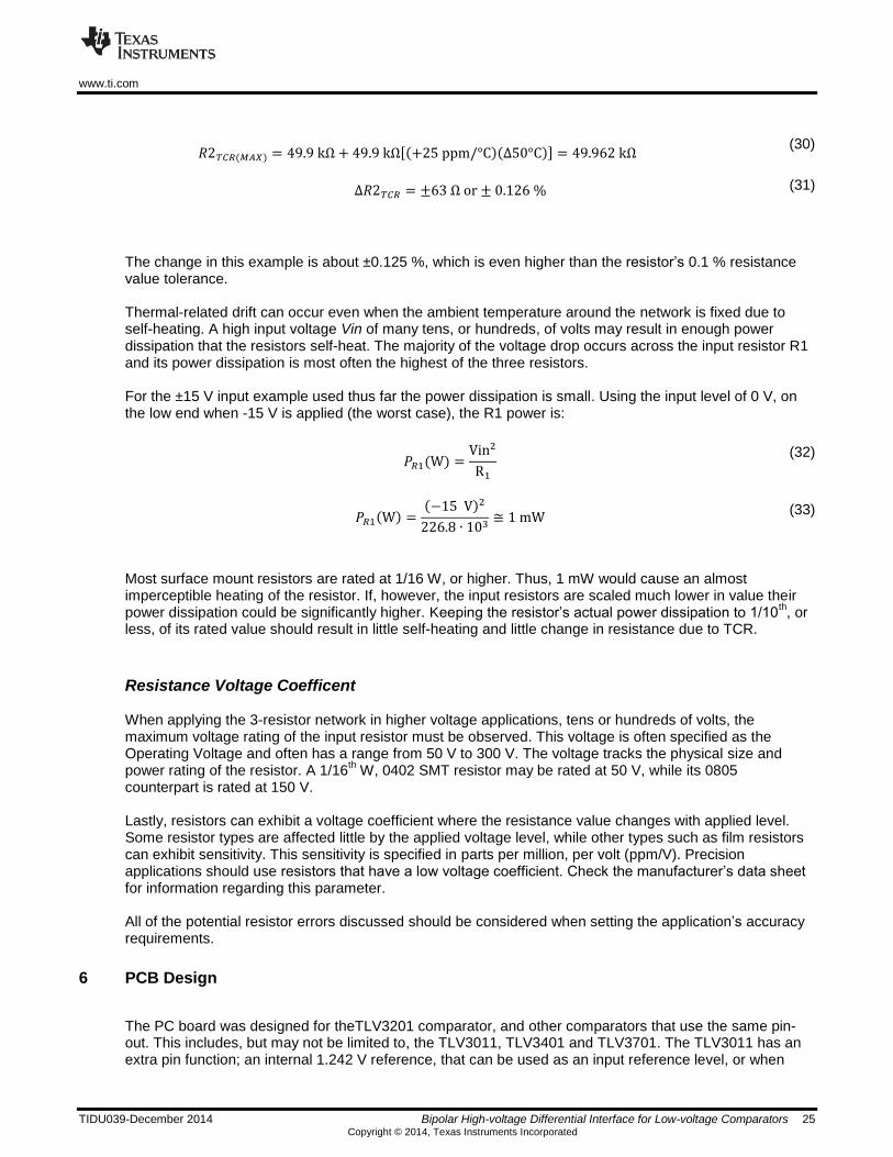
Table 2 - Summary of measured dc levels obtained at the comparator inputs
The voltages at the Vcmp+ and Vcmp- circuit points fell within the predicted worst-case range for each applied input voltage level. Interestingly, the error was least with -15 V input and most at +15 V input, with 0 V between them. The TLV3201 was connected in the circuit during these dc measurements. It would have minimal influence on the measured results.
7.2 AC test measurements
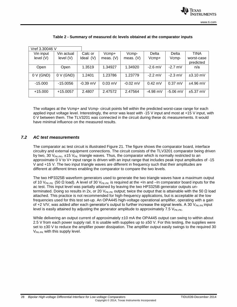
The comparator ac test circuit is illustrated Figure 21. The figure shows the comparator board, interface circuitry and external equipment connections. The circuit consists of the TLV3201 comparator being driven by two, 30 VPK-PK, ±15 VPK triangle waves. Thus, the comparator which is normally restricted to an approximate 0 V to V+ input range is driven with an input range that includes peak input amplitudes of -15 V and +15 V. The two input triangle waves are different in frequency such that their amplitudes are different at different times enabling the comparator to compare the two levels. The two HP3325B waveform generators used to generate the two triangle waves have a maximum output of 10 VPK-PK (50 Ω load). A level of 30 VPK-PK is required at the +In and –In comparator board inputs for the ac test. This input level was partially attained by leaving the two HP3325B generator outputs un-terminated. Doing so results in 2x, or 20 VPK-PK output; twice the output that is attainable with the 50 Ω load attached. This practice is not recommended for high-frequency applications, but is acceptable at the low frequencies used for this test set-up. An OPA445 high-voltage operational amplifier, operating with a gain of +2 V/V, was added after each generator’s output to further increase the signal levels. A 30 VPK-PK input level is easily attained by adjusting the generator amplitude to approximately 7.5 VPK-PK. While delivering an output current of approximately ±10 mA the OPA445 output can swing to within about 2.5 V from each power supply rail. It is usable with supplies up to ±50 V. For this testing, the supplies were set to ±30 V to reduce the amplifier power dissipation. The amplifier output easily swings to the required 30 VPK-PK with this supply level.
Vref 3.30046 V
Vin input level (V)
Vin actual level (V)
Calc or Ideal (V)
Vcmp+ meas. (V)
Vcmp- meas. (V)
Delta Vcmp+
Delta Vcmp-
TINA worst-case predicted
Open Open 1.3519 1.34927 1.34920 -2.6 mV -2.7 mV n/a
0 V (GND) 0 V (GND) 1.2401 1.23786 1.23779 -2.2 mV -2.3 mV ±3.10 mV
-15.000 -15.0056 -0.39 mV 0.03 mV -0.02 mV 0.42 mV 0.37 mV ±4.96 mV
+15.000 +15.0057 2.4807 2.47572 2.47564 -4.98 mV -5.06 mV ±5.37 mV
www.ti.com
TIDU039-December 2014 Bipolar High-voltage Differential Interface for Low-voltage Comparators 29 Copyright © 2014, Texas Instruments Incorporated
Figure 21 - High-voltage differential input ac test circuit
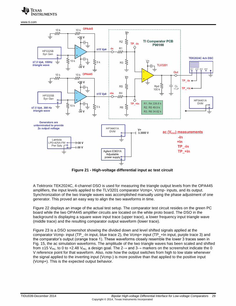
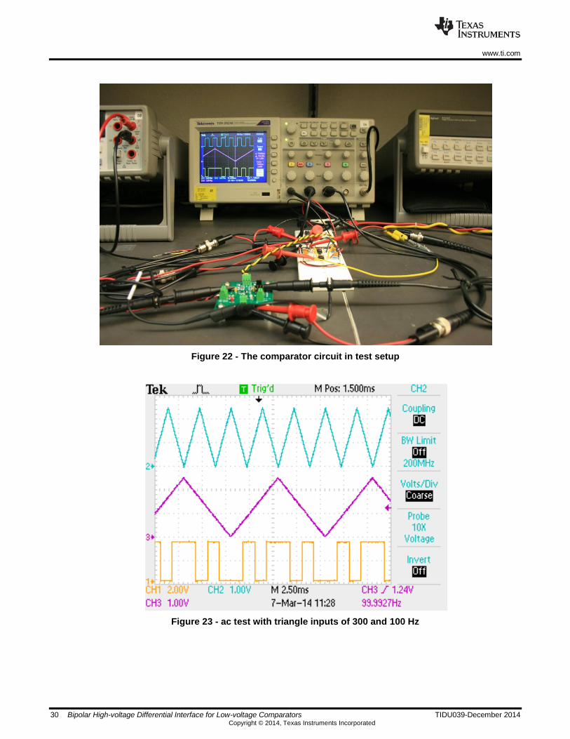
A Tektronix TEK2024C, 4-channel DSO is used for measuring the triangle output levels from the OPA445 amplifiers, the input levels applied to the TLV3201 comparator Vcmp+, Vcmp- inputs, and its output. Synchronization of the two triangle waves was accomplished manually using the phase adjustment of one generator. This proved an easy way to align the two waveforms in time. Figure 22 displays an image of the actual test setup. The comparator test circuit resides on the green PC board while the two OPA445 amplifier circuits are located on the white proto board. The DSO in the background is displaying a square wave input trace (upper trace), a lower frequency input triangle wave (middle trace) and the resulting comparator output waveform (lower trace). Figure 23 is a DSO screenshot showing the divided down and level shifted signals applied at the comparator Vcmp- input (TP_-In input, blue trace 2), the Vcmp+ input (TP_+In input, purple trace 3) and the comparator’s output (orange trace 1). These waveforms closely resemble the lower 3 traces seen in Fig. 15, the ac simulation waveforms. The amplitude of the two triangle waves has been scaled and shifted from ±15 VPK, to 0 to +2.48 VPK, a design goal. The 2→ and 3→ markers on the screenshot indicate the 0 V reference point for that waveform. Also, note how the output switches from high to low state whenever the signal applied to the inverting input (Vcmp-) is more positive than that applied to the positive input (Vcmp+). This is the expected output behavior.
www.ti.com
30 Bipolar High-voltage Differential Interface for Low-voltage Comparators TIDU039-December 2014 Copyright © 2014, Texas Instruments Incorporated
Figure 22 - The comparator circuit in test setup
Figure 23 - ac test with triangle inputs of 300 and 100 Hz
www.ti.com
TIDU039-December 2014 Bipolar High-voltage Differential Interface for Low-voltage Comparators 31 Copyright © 2014, Texas Instruments Incorporated
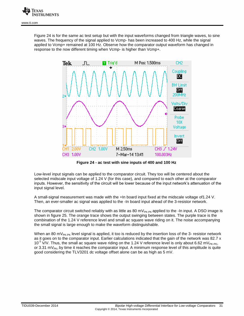
Figure 24 is for the same ac test setup but with the input waveforms changed from triangle waves, to sine waves. The frequency of the signal applied to Vcmp- has been increased to 400 Hz, while the signal applied to Vcmp+ remained at 100 Hz. Observe how the comparator output waveform has changed in response to the now different timing when Vcmp- is higher than Vcmp+.
Figure 24 - ac test with sine inputs of 400 and 100 Hz
Low-level input signals can be applied to the comparator circuit. They too will be centered about the selected midscale input voltage of 1.24 V (for this case), and compared to each other at the comparator inputs. However, the sensitivity of the circuit will be lower because of the input network’s attenuation of the input signal level. A small-signal measurement was made with the +In board input fixed at the midscale voltage of1.24 V. Then, an ever-smaller ac signal was applied to the -In board input ahead of the 3-resistor network. The comparator circuit switched reliably with as little as 80 mVPK-PK applied to the -In input. A DSO image is shown in figure 25. The orange trace shows the output swinging between states. The purple trace is the combination of the 1.24 V reference level and small ac square wave riding on it. The noise accompanying the small signal is large enough to make the waveform distinguishable. When an 80 mVPK-PK level signal is applied, it too is reduced by the insertion loss of the 3- resistor network as it goes on to the comparator input. Earlier calculations indicated that the gain of the network was 82.7 x 10
-3 V/V. Thus, the small ac square wave riding on the 1.24 V reference level is only about 6.62 mVPK-PK,
or 3.31 mVPK, by time it reaches the comparator input. A minimum response level of this amplitude is quite good considering the TLV3201 dc voltage offset alone can be as high as 5 mV.

www.ti.com
32 Bipolar High-voltage Differential Interface for Low-voltage Comparators TIDU039-December 2014 Copyright © 2014, Texas Instruments Incorporated
Figure 25 - Comparator small signal input level test
8 Modifications
The 3-resistor network developed for this comparator application has uses in other applications. A couple of ideas are presented here.
8.1 High Voltage Zero Crossing Detector
The differential bipolar HV, to unipolar LV comparator circuit can be used in applications where one input
can be referenced to either a resistor divider, or a voltage reference, depending on the required accuracy.
The other input is driven in a single-ended manner from a single 3-resistor network to which the HV is
applied. The TLV3011 CMOS comparator is ideally suited for this type of application because it includes a
high accuracy 1.242 V internal voltage reference.
Figure 29 is the schematic of the TLV3011 comparator connected in this manner as zero-crossing detector. The 3-resistor network is designed for a 0 to 2.482 V (2x1.242 V) input range such that its mid-scale voltage is close the 1.242 V applied to the non-inverting input.
A REF3333, high accuracy +3.3 V voltage reference, powers the TLV3011. It not only powers to the TLV3011, but also provides the output pull-up voltage. More importantly, it provides a precision +3.3 V reference level to bias the 3-resistor network connected to the comparator’s inverting input.
The example circuit shown in Figure 29 has been designed to detect the 0 V crossing of a 50/60 Hz ac line signal having an RMS voltage of 120 V, or 170 VPK.

www.ti.com
TIDU039-December 2014 Bipolar High-voltage Differential Interface for Low-voltage Comparators 33 Copyright © 2014, Texas Instruments Incorporated
Figure 29 - High Voltage Zero Crossing Detector
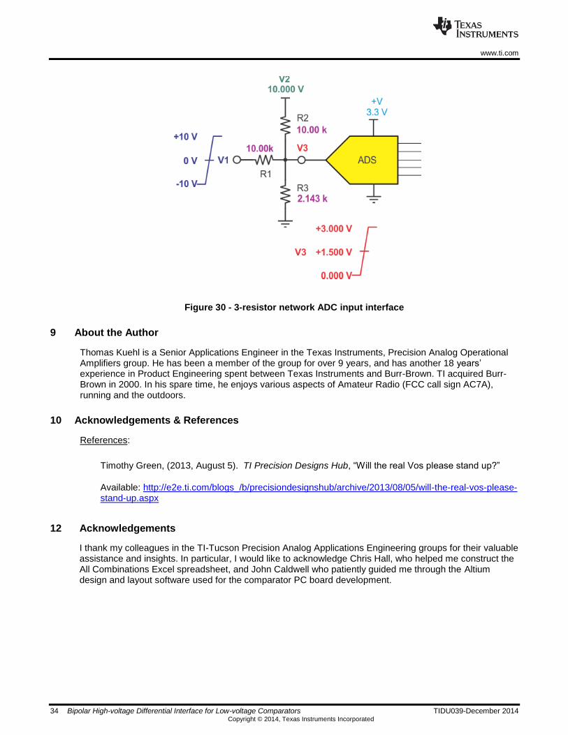
8.2 3-Resistor ADC interface
Another possible application that comes to mind is using the 3-resistor network for interfacing a ±5 V, or ±10 V, sensor output to the input of low voltage analog-to-digital converters (ADC). The idea is illustrated in figure 30 where a ±10 V input range is transformed to a 0 to 3.000 V range.
The positive aspects of this solution are simplicity, low cost, exclusion of an active device that could too affect linearity. In addition, a true 0-volt, input level can be achieved. Most any bipolar input voltage range can be accommodated; levels well beyond the ±10 V illustrated in figure 30. Just as with the comparator circuit two, 3-resistor networks could be applied a differential input ADC.
Some possible drawbacks are the gain and offset accuracies are directly affected by the resistor values and their preciseness, a separate higher voltage (> 2x V3) is needed for V2 and the high resistances represent a high source impedance. The latter can be an issue because the input switching behavior of an ADS (ADC) is very dynamic changing the input impedance across the conversion cycle. A buffer amplifier might be needed between the network and ADS to provide the transient current demands. If the input sensor is relatively slow, and a suitable ADC is teamed up with it, this simple interface may provide a practical, minimum component interface.
www.ti.com
34 Bipolar High-voltage Differential Interface for Low-voltage Comparators TIDU039-December 2014 Copyright © 2014, Texas Instruments Incorporated
Figure 30 - 3-resistor network ADC input interface
9 About the Author
Thomas Kuehl is a Senior Applications Engineer in the Texas Instruments, Precision Analog Operational Amplifiers group. He has been a member of the group for over 9 years, and has another 18 years’ experience in Product Engineering spent between Texas Instruments and Burr-Brown. TI acquired Burr-Brown in 2000. In his spare time, he enjoys various aspects of Amateur Radio (FCC call sign AC7A), running and the outdoors.
10 Acknowledgements & References
References:
Timothy Green, (2013, August 5). TI Precision Designs Hub, “Will the real Vos please stand up?”
Available: http://e2e.ti.com/blogs_/b/precisiondesignshub/archive/2013/08/05/will-the-real-vos-please-stand-up.aspx
12 Acknowledgements
I thank my colleagues in the TI-Tucson Precision Analog Applications Engineering groups for their valuable assistance and insights. In particular, I would like to acknowledge Chris Hall, who helped me construct the All Combinations Excel spreadsheet, and John Caldwell who patiently guided me through the Altium design and layout software used for the comparator PC board development.
www.ti.com
TIDU039-December 2014 Bipolar High-voltage Differential Interface for Low-voltage Comparators 35 Copyright © 2014, Texas Instruments Incorporated
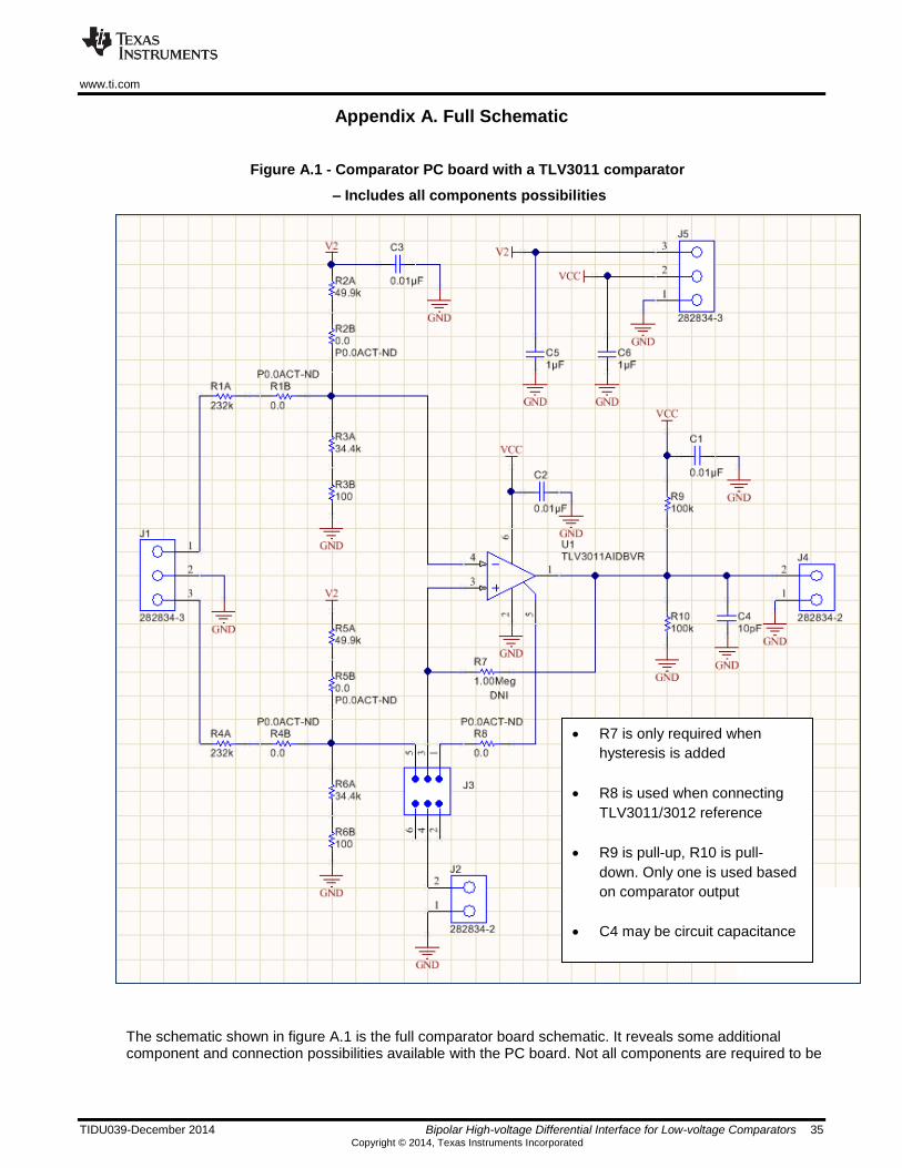
Appendix A. Full Schematic
Figure A.1 - Comparator PC board with a TLV3011 comparator
– Includes all components possibilities
The schematic shown in figure A.1 is the full comparator board schematic. It reveals some additional component and connection possibilities available with the PC board. Not all components are required to be
R7 is only required when
hysteresis is added
R8 is used when connecting
TLV3011/3012 reference
R9 is pull-up, R10 is pull-
down. Only one is used based
on comparator output
C4 may be circuit capacitance
www.ti.com
36 Bipolar High-voltage Differential Interface for Low-voltage Comparators TIDU039-December 2014 Copyright © 2014, Texas Instruments Incorporated
populated and just those needed should be. The board schematic shows the parts connections when used.
A TLV3011 CMOS comparator is shown in place of the TLV3201 used in the tests. The TLV3011 comparator includes a precision 1.242 V reference. It can be employed directly as a reference level in the comparator circuit, or used for another purpose. Here is circuit connection information for the comparator board:
A shorting jumper may be connected between J3 pins 1 and 3 to make the connection between
the TLV3011 reference voltage pin and non-inverting input, pin 3. Then, the 3-resistor network is
disconnected from the comparator’s non-inverting input.
R7 may be connected into the circuit to add some positive feedback (hysteresis) to the non-
inverting input for comparators such as the TLV3201, TLV3401 and TLV3701. The R7 value
would have to be selected in conjunction with the resistors used in the non-inverting, 3-resistor
network. An exercise left for the reader!
R7 and R8 may be used in conjunction with the TLV3011 reference pin to apply hysteresis to the
comparator. The J3, pin 3 to pin 1, jumper would be required.
An external dc source, or ac signal, may be applied directly to the non-inverting input via J2.
Make sure that the levels are within the normal, specified range for the comparator used. When in
this mode the 3-resistor network is not in the circuit. A shorting jumper would be connected
between J3 pins 3 and 4.
R9 is a pull-up resistor for open drain/collector output comparators such as the TLV3401 and
TLV3011. R10 is a pull down resistor, but really isn’t necessarily required for push-pull output
comparators such as the TLV3012, TLV3201, and TLV3701. It provides an opportunity to load the
output and drive current into a grounded load.
The 3-resistor networks, with the exception of one resistor value that is preselected, are likely to require nonstandard resistance values. Therefore, using two separate resistors to make up a nonstandard value may be a more practical solution. In the previous examples, R2 and R5 were selected as standard value 49.9 k Ω resistors, while the others were a series combination of two standard resistor values. All the resistors that make up the 3-resistor networks on the PC board are divided into two separate resistor replacements such as R1A and R1B, R4A and R4B, etc. The two sections are placed in series because it is much easier to sum discrete standard values, than to derive a parallel equivalent value. In addition, placing them in series divides the high-voltage across the two resistors in proportion to their resistances. This is not the case when they are parallel-connected. The full high-voltage is born by both resistors.
www.ti.com
TIDU039-December 2014 Bipolar High-voltage Differential Interface for Low-voltage Comparators 37 Copyright © 2014, Texas Instruments Incorporated
Appendix B. Populated Schematic
The comparator interface circuit and PC board were designed to use not only the TLV3201, but other comparators that share its pin-out pattern such as the TLV3011, TLV3401 and TLV3701. The TLV3011 has an extra pin function, an internal 1.242 V reference, which was described earlier. The exact TLV3201 circuit used for testing the comparator circuit can be seen in figure 26. The circuit flow, left to right, begins with J1 where the two input signals to be compared are applied. It then passes to the two, 3-resistor networks. The output from these networks is precisely attenuated and level-shifted to allow direct interface with the TLV3201 comparator input range. The comparator output appears at J4. The 3-resistor network resistor values are selected to suite the particular application requirements. 0.01 uF power supply decoupling capacitors are placed across the resistor dividers Vref to ground, and from the TLV3201 Vcc pin to ground. Additional 1 uF power supply decoupling capacitors are located at the J5 power supply terminal block. The TLV3201 output has a 100 kΩ resistor and a 10 pF capacitor to ground. V+ provides voltage to the TLV3201 Vcc pin. Be sure to connect a shorting jumper between the J3, pins 3 and 5. Otherwise, an intended input level will not be connected to the comparator’s non-inverting input.

www.ti.com
38 Bipolar High-voltage Differential Interface for Low-voltage Comparators TIDU039-December 2014 Copyright © 2014, Texas Instruments Incorporated
Figure 26 – TLV3201 test circuit configuration set-up on PC board
Figure 27 is an image of the populated comparator PC board set up for the TLV3201 circuit in figure 26. The two, 3-resistor networks are comprised of standard value 0.1 % tolerance resistors of an individual value, or a series combination, whatever worked out to arrive as close as possible to the required value. R2A and R5A have a degree of freedom that the other resistors don’t and may be selected as a single, standard value precision resistor.

www.ti.com
TIDU039-December 2014 Bipolar High-voltage Differential Interface for Low-voltage Comparators 39 Copyright © 2014, Texas Instruments Incorporated
Figure 27 - PC board with the components shown in figure 26

www.ti.com
40 Bipolar High-voltage Differential Interface for Low-voltage Comparators TIDU039-December 2014 Copyright © 2014, Texas Instruments Incorporated
Appendix C – Bill of Materials for TLV3201 Comparator Test Board
Table C-1
Item Quantity Value Designator Description Manufacturer Manufacturer Part Number Supplier Part Number
1 4 0.01uF C1, C2, C3, C5
CAP, CERM, 0.01uF, 100V, +/-10%, X7R, 0805
TDK Corporation
C2012X7R2A103K085AA 445-1343-1-ND
2 1 10pF C4
CAP, CERM, 10pF, 100V, +/-5%, C0G/NP0, 0805
Kemet C0805C100J1GACTU 399-1109-1-ND
3 2 1uF C6, C7 CAP, CERM, 1uF, 25V, +/-10%, X7R, 1206
AVX Corporation
12063C105KAT2A 478-1567-1-ND
4 2 J1, J5 3 contact eurostyle terminal block
TE Connectivity
282834-3 A98334-ND
5 2 J2, J4 2 contact eurostyle terminal block
TE Connectivity
282834-2 A98333-ND
6 1 J3
Header, TH, 100mil, 3x2, Gold plated, 230 mil above insulator
Samtec Inc TSW-103-07-G-D SAM1028-03-ND
7 2 220k R1A, R4A RES, 220k ohm, 0.1%, 0.125W, 0805 SMD
Panasonic Electronic Components
ERA-6AEB224V P220KDATR-ND
8 2 6.8k R1B, R4B RES, 6.8k ohm, 0.1%, 0.125W, 0805 SMD
Panasonic Electronic Components
ERA-6AEB682V P6.8KDATR-ND
9 2 49.9k R2A, R5A RES 49.9K OHM 1/8W .1% 0805 SMD
Panasonic Electronic Components
ERA-6AEB4992V P49.9KDACT-ND
10 2 0.0 R2B, R5B RES 0.0 OHM 1/8W JUMP 0805 SMD
Panasonic Electronic Components
ERJ-6GEY0R00V P0.0ACT-ND
11 1 34.0k R3A RES, 34k ohm, 0.1%, 0.125W, 0805 SMD
Panasonic Electronic Components
ERA-6AEB3402V P34KDATR-ND
12 2 620 ohm R3B, R6B RES, 620 ohm, 0.1%, 0.125W, 0805 SMD
Panasonic Electronic Components
ERA-6AEB621V P620DATR-ND
13 1 34.0k R6A RES, 34k ohm, 0.1%, 0.125W, 0805 SMD
Panasonic Electronic Components
ERA-6AEB3402V P34KDATR-ND
14 1 100k R10 RES, 100k ohm, 5%, 0.125W, 0805
Vishay Dale CRCW0805100KJNEA 541-100KACT-ND
15 1 1x2 SH-1 Shunt, 100mil, Flash Gold, Black
Sullins Connector Solutions
SPC02SYAN S9001-ND
16 4 TP +In, TP -In, TP Out, TP V2
TEST POINT - RED
Keystone Electronics
5005 5005K-ND
17 1 U1
40-ns, microPOWER, Push-Pull Output Comparator
Texas Instruments
TLV3201AIDBVR 296-36750-1-ND

www.ti.com
TIDU039-December 2014 Bipolar High-voltage Differential Interface for Low-voltage Comparators 41 Copyright © 2014, Texas Instruments Incorporated
Appendix D - All Combinations Worst-Case Analysis
This Worst-Case analysis is more exact than the TINA-Spice analysis. It provides numeric, Vdiff error voltage levels attainable for all resistor combinations extremes based on the 0.1 % tolerance, or another specified tolerance. Since there are 6 resistors, 64 (2
6) combinations are possible.
The analysis starts with all 6 resistors set to the low extreme values and ends with all of them set to the high extreme values. Sequencing from the lowest to highest resistor values is accomplished in a binary fashion starting with all zeros and ending with all ones. A resistor is set to the low extreme when a “0” is encountered in the binary count and to the high extreme when a “1” is encountered. The results can be reviewed in the Excel file having tab named “All Combinations.” The analysis is set up with Vin (V1) set to 0 V, and Vref (V2) set to 3.3 V; however, they can be set to whatever levels are required. Since there are two, 3-resistor networks there are two outputs, V3 and V4. The difference between them is a differential voltage listed as Vdiff in the All Combinations spreadsheet. It can be seen that the worst-case differential voltages are ±3.1 mV, when Vin is 0 V and Vref is 3.3 V. This spread is twice that obtained with the single 3-resistor network and is expected since there are two networks contributing error. The numerical values associated with Vdiff are listed in the Excel file. A graph was created plotting the worst-case low, through worst-case high resistor combinations in order from 0 to 63. It can be viewed in the Excel file “Graphs” tab. This graph is presented here in figure C1.
Figure D1 - All combinations results for 0.1 % tolerance resistors
This worst-case error voltage plot is only valid for Vin = 0V, and Vref = 3.3 V. If either voltage is changed the error levels will change and a completely different error pattern can result. This may be observed by changing the voltages entered in the All Combinations spreadsheet.
-0.00400
-0.00300
-0.00200
-0.00100
0.00000
0.00100
0.00200
0.00300
0.00400
0 8 16 24 32 40 48 56 64
Vo
ltag
e e
rro
r (V
)
Resistor combination no.
Differential voltage error for two, 3-resistor networks
IMPORTANT NOTICE FOR TI REFERENCE DESIGNSTexas Instruments Incorporated ("TI") reference designs are solely intended to assist designers (“Buyers”) who are developing systems thatincorporate TI semiconductor products (also referred to herein as “components”). Buyer understands and agrees that Buyer remainsresponsible for using its independent analysis, evaluation and judgment in designing Buyer’s systems and products.TI reference designs have been created using standard laboratory conditions and engineering practices. TI has not conducted anytesting other than that specifically described in the published documentation for a particular reference design. TI may makecorrections, enhancements, improvements and other changes to its reference designs.Buyers are authorized to use TI reference designs with the TI component(s) identified in each particular reference design and to modify thereference design in the development of their end products. HOWEVER, NO OTHER LICENSE, EXPRESS OR IMPLIED, BY ESTOPPELOR OTHERWISE TO ANY OTHER TI INTELLECTUAL PROPERTY RIGHT, AND NO LICENSE TO ANY THIRD PARTY TECHNOLOGYOR INTELLECTUAL PROPERTY RIGHT, IS GRANTED HEREIN, including but not limited to any patent right, copyright, mask work right,or other intellectual property right relating to any combination, machine, or process in which TI components or services are used.Information published by TI regarding third-party products or services does not constitute a license to use such products or services, or awarranty or endorsement thereof. Use of such information may require a license from a third party under the patents or other intellectualproperty of the third party, or a license from TI under the patents or other intellectual property of TI.TI REFERENCE DESIGNS ARE PROVIDED "AS IS". TI MAKES NO WARRANTIES OR REPRESENTATIONS WITH REGARD TO THEREFERENCE DESIGNS OR USE OF THE REFERENCE DESIGNS, EXPRESS, IMPLIED OR STATUTORY, INCLUDING ACCURACY ORCOMPLETENESS. TI DISCLAIMS ANY WARRANTY OF TITLE AND ANY IMPLIED WARRANTIES OF MERCHANTABILITY, FITNESSFOR A PARTICULAR PURPOSE, QUIET ENJOYMENT, QUIET POSSESSION, AND NON-INFRINGEMENT OF ANY THIRD PARTYINTELLECTUAL PROPERTY RIGHTS WITH REGARD TO TI REFERENCE DESIGNS OR USE THEREOF. TI SHALL NOT BE LIABLEFOR AND SHALL NOT DEFEND OR INDEMNIFY BUYERS AGAINST ANY THIRD PARTY INFRINGEMENT CLAIM THAT RELATES TOOR IS BASED ON A COMBINATION OF COMPONENTS PROVIDED IN A TI REFERENCE DESIGN. IN NO EVENT SHALL TI BELIABLE FOR ANY ACTUAL, SPECIAL, INCIDENTAL, CONSEQUENTIAL OR INDIRECT DAMAGES, HOWEVER CAUSED, ON ANYTHEORY OF LIABILITY AND WHETHER OR NOT TI HAS BEEN ADVISED OF THE POSSIBILITY OF SUCH DAMAGES, ARISING INANY WAY OUT OF TI REFERENCE DESIGNS OR BUYER’S USE OF TI REFERENCE DESIGNS.TI reserves the right to make corrections, enhancements, improvements and other changes to its semiconductor products and services perJESD46, latest issue, and to discontinue any product or service per JESD48, latest issue. Buyers should obtain the latest relevantinformation before placing orders and should verify that such information is current and complete. All semiconductor products are soldsubject to TI’s terms and conditions of sale supplied at the time of order acknowledgment.TI warrants performance of its components to the specifications applicable at the time of sale, in accordance with the warranty in TI’s termsand conditions of sale of semiconductor products. Testing and other quality control techniques for TI components are used to the extent TIdeems necessary to support this warranty. Except where mandated by applicable law, testing of all parameters of each component is notnecessarily performed.TI assumes no liability for applications assistance or the design of Buyers’ products. Buyers are responsible for their products andapplications using TI components. To minimize the risks associated with Buyers’ products and applications, Buyers should provideadequate design and operating safeguards.Reproduction of significant portions of TI information in TI data books, data sheets or reference designs is permissible only if reproduction iswithout alteration and is accompanied by all associated warranties, conditions, limitations, and notices. TI is not responsible or liable forsuch altered documentation. Information of third parties may be subject to additional restrictions.Buyer acknowledges and agrees that it is solely responsible for compliance with all legal, regulatory and safety-related requirementsconcerning its products, and any use of TI components in its applications, notwithstanding any applications-related information or supportthat may be provided by TI. Buyer represents and agrees that it has all the necessary expertise to create and implement safeguards thatanticipate dangerous failures, monitor failures and their consequences, lessen the likelihood of dangerous failures and take appropriateremedial actions. Buyer will fully indemnify TI and its representatives against any damages arising out of the use of any TI components inBuyer’s safety-critical applications.In some cases, TI components may be promoted specifically to facilitate safety-related applications. With such components, TI’s goal is tohelp enable customers to design and create their own end-product solutions that meet applicable functional safety standards andrequirements. Nonetheless, such components are subject to these terms.No TI components are authorized for use in FDA Class III (or similar life-critical medical equipment) unless authorized officers of the partieshave executed an agreement specifically governing such use.Only those TI components that TI has specifically designated as military grade or “enhanced plastic” are designed and intended for use inmilitary/aerospace applications or environments. Buyer acknowledges and agrees that any military or aerospace use of TI components thathave not been so designated is solely at Buyer's risk, and Buyer is solely responsible for compliance with all legal and regulatoryrequirements in connection with such use.TI has specifically designated certain components as meeting ISO/TS16949 requirements, mainly for automotive use. In any case of use ofnon-designated products, TI will not be responsible for any failure to meet ISO/TS16949.
Mailing Address: Texas Instruments, Post Office Box 655303, Dallas, Texas 75265Copyright © 2014, Texas Instruments Incorporated


![Bipolar PPT for OHSU Grand Rounds 10-25-2016 [Read-Only] · PDF filePrimary Care Assessment and ... TOP = topiramate GBT = gabapentin ... in your differential diagnosis Antidepressant](https://static.fdocuments.us/doc/165x107/5a7367377f8b9abb538e96b6/bipolar-ppt-for-ohsu-grand-rounds-10-25-2016-read-only-primary-care-assessment.jpg)