BFP840FESD Low Noise Amplifier for 3.4GHz- 3.8GHz (Band 42 ...
26
RF and Protection Devices BFP840FESD Technical Report TR1129 Revision: Rev. 1.1 2013-06-05 Low Noise Amplifier for 3.4GHz- 3.8GHz (Band 42/ 43)
Transcript of BFP840FESD Low Noise Amplifier for 3.4GHz- 3.8GHz (Band 42 ...

RF and Protect ion Devices
BFP840FESD
Technical Report TR1129 Revision: Rev. 1.1
2013-06-05
Low Noise Ampl i f ier for 3.4GHz- 3.8GHz (Band 42/ 43)

Edition 2013-06-05
Published by Infineon Technologies AG 81726 Munich, Germany
© 2013 Infineon Technologies AG All Rights Reserved.
Legal Disclaimer
The information given in this document shall in no event be regarded as a guarantee of conditions or characteristics. With respect to any examples or hints given herein, any typical values stated herein and/or any information regarding the application of the device, Infineon Technologies hereby disclaims any and all warranties and liabilities of any kind, including without limitation, warranties of non-infringement of intellectual property rights of any third party.
Information
For further information on technology, delivery terms and conditions and prices, please contact the nearest Infineon Technologies Office (www.infineon.com).
Warnings
Due to technical requirements, components may contain dangerous substances. For information on the types in question, please contact the nearest Infineon Technologies Office.
Infineon Technologies components may be used in life-support devices or systems only with the express written approval of Infineon Technologies, if a failure of such components can reasonably be expected to cause the failure of that life-support device or system or to affect the safety or effectiveness of that device or system. Life support devices or systems are intended to be implanted in the human body or to support and/or maintain and sustain and/or protect human life. If they fail, it is reasonable to assume that the health of the user or other persons may be endangered.

BFP840FESD Low Noise Amplifier for 3.4GHz- 3.8GHz
Technical Report, Rev. 1.1 2013-06-05 3 / 26
Technical Report TR1129
Revision History: 2013-06-05
Previous Revision:
Page Subjects (major changes since last revision)
17 to 22 Figure 17 to Figure 28: Temperature measurement results are included
Trademarks of Infineon Technologies AG
AURIX™, C166™, CanPAK™, CIPOS™, CIPURSE™, EconoPACK™, CoolMOS™, CoolSET™, CORECONTROL™, CROSSAVE™, DAVE™, DI-POL™, EasyPIM™, EconoBRIDGE™, EconoDUAL™, EconoPIM™, EconoPACK™, EiceDRIVER™, eupec™, FCOS™, HITFET™, HybridPACK™, I²RF™, ISOFACE™, IsoPACK™, MIPAQ™, ModSTACK™, my-d™, NovalithIC™, OptiMOS™, ORIGA™, POWERCODE™, PRIMARION™, PrimePACK™, PrimeSTACK™, PRO-SIL™, PROFET™, RASIC™, ReverSave™, SatRIC™, SIEGET™, SINDRION™, SIPMOS™, SmartLEWIS™, SOLID FLASH™, TEMPFET™, thinQ!™, TRENCHSTOP™, TriCore™.
Other Trademarks
Advance Design System™ (ADS) of Agilent Technologies, AMBA™, ARM™, MULTI-ICE™, KEIL™, PRIMECELL™, REALVIEW™, THUMB™, µVision™ of ARM Limited, UK. AUTOSAR™ is licensed by AUTOSAR development partnership. Bluetooth™ of Bluetooth SIG Inc. CAT-iq™ of DECT Forum. COLOSSUS™, FirstGPS™ of Trimble Navigation Ltd. EMV™ of EMVCo, LLC (Visa Holdings Inc.). EPCOS™ of Epcos AG. FLEXGO™ of Microsoft Corporation. FlexRay™ is licensed by FlexRay Consortium. HYPERTERMINAL™ of Hilgraeve Incorporated. IEC™ of Commission Electrotechnique Internationale. IrDA™ of Infrared Data Association Corporation. ISO™ of INTERNATIONAL ORGANIZATION FOR STANDARDIZATION. MATLAB™ of MathWorks, Inc. MAXIM™ of Maxim Integrated Products, Inc. MICROTEC™, NUCLEUS™ of Mentor Graphics Corporation. MIPI™ of MIPI Alliance, Inc. MIPS™ of MIPS Technologies, Inc., USA. muRata™ of MURATA MANUFACTURING CO., MICROWAVE OFFICE™ (MWO) of Applied Wave Research Inc., OmniVision™ of OmniVision Technologies, Inc. Openwave™ Openwave Systems Inc. RED HAT™ Red Hat, Inc. RFMD™ RF Micro Devices, Inc. SIRIUS™ of Sirius Satellite Radio Inc. SOLARIS™ of Sun Microsystems, Inc. SPANSION™ of Spansion LLC Ltd. Symbian™ of Symbian Software Limited. TAIYO YUDEN™ of Taiyo Yuden Co. TEAKLITE™ of CEVA, Inc. TEKTRONIX™ of Tektronix Inc. TOKO™ of TOKO KABUSHIKI KAISHA TA. UNIX™ of X/Open Company Limited. VERILOG™, PALLADIUM™ of Cadence Design Systems, Inc. VLYNQ™ of Texas Instruments Incorporated. VXWORKS™, WIND RIVER™ of WIND RIVER SYSTEMS, INC. ZETEX™ of Diodes Zetex Limited.
Last Trademarks Update 2011-11-11

BFP840FESD
Low Noise Amplifier for 3.4GHz- 3.8GHz
Technical Report, Rev. 1.1 2013-06-05 4 / 26
Table of Content
1 Application Circuit and Performance Overview .............................................................................. 5 1.1 Summary of Measurement Results ...................................................................................................... 5 1.2 High Gain Low Noise Amplifier using BFP840FESD for 3.4 – 3.8 GHz LTE Application .................... 6 1.3 Schematics and Bill-of-Materials .......................................................................................................... 8
2 Measured Graphs ............................................................................................................................. 10
3 Evaluation Board and layout Information ...................................................................................... 23
4 Authors .............................................................................................................................................. 25
List of Figures
Figure 1 Package and pin connections of BFP840FESD in Topview ................................................................ 6 Figure 2 Schematics of BFP840FESD Low Noise Amplifier for 3.4 – 3.8 GHz Application ............................... 8 Figure 3 Insertion Power Gain of the 3.4 – 3.8 GHz LNA with BFP840FESD ................................................. 10 Figure 4 Wideband Insertion Power Gain of the 3.4 – 3.8 GHz LNA with BFP840FESD ................................ 10 Figure 5 Noise Figure of BFP840FESD LNA for 3400 - 2500 MHz ................................................................. 11 Figure 6 Reverse Isolation of the 3.4 – 3.8 GHz LNA with BFP840FESD ....................................................... 11 Figure 7 Input Matching of the 3.4 – 3.8 GHz LNA with BFP840FESD ........................................................... 12 Figure 8 Input Matching of the 3.4 – 3.8 GHz LNA with BFP840FESD (Smith Chart) .................................... 12 Figure 9 Output Matching of the 3.4 – 3.8 GHz LNA with BFP840FESD ........................................................ 13 Figure 10 Output Matching of the 3.4 – 3.8 GHz LNA with BFP840FESD (Smith Chart) .................................. 13 Figure 11 Wideband Stability k Factor of the 3.4 – 3.8 GHz LNA with BFP840FESD ....................................... 14 Figure 12 Wideband Stability Mu Factor of the 3.4 – 3.8 GHz LNA with BFP840FESD.................................... 14 Figure 13 1dB Compression Point of the BFP840FESD Circuit at 3600 MHz ................................................... 15 Figure 14 Output 3
rd Order Intercept Point of BFP840FESD at 3600 MHz ........................................................ 15
Figure 15 OFF-Mode (Vcc = 0V, Icc = 0mA) S21 of the 3.4 – 3.8 GHz LNA with BFP840FESD ...................... 16 Figure 16 OFF-Mode (Vcc = 0V, Icc = 0mA) S21 of the 3.4 – 3.8 GHz LNA with BFP840FESD ...................... 16 Figure 17 Bias current in the Temperature Range from -40˚C to 85˚C (Vcc=3.0 V) ......................................... 17 Figure 18 Noise Figure of BFP840FESD LNA in the Temperature Range from -40˚C to 85˚C (Vcc=3.0V) .... 17 Figure 19 BFP840FESD LNA Insertion Power Gain in the Temperature Range from -40˚C to 85˚C (Vcc=3.0
V) ........................................................................................................................................................ 18 Figure 20 BFP840FESD LNA Reverse Isolation in the Temperature Range from -40˚C to 85˚C (Vcc=3.0V) 18 Figure 21 BFP840FESD LNA Input Matching in the Temperature Range from -40˚C to 85˚C (Vcc=3.0 V) .... 19 Figure 22 BFP840FESD LNA Input Matching in the Temperature Range from -40˚C to 85˚C (Smith Chart)
(Vcc=3.0 V) ........................................................................................................................................ 19 Figure 23 BFP840FESD LNA Output Matching in the Temperature Range from -40˚C to 85˚C (Vcc=3.0V) ... 20 Figure 24 BFP840FESD LNA Output Matching in the temperature range from -40 ˚C to 85 ˚C (Smith Chart)
(Vcc=3.0 V) ........................................................................................................................................ 20 Figure 25 1dB Compression Point of the BFP840FESD LNA at 3.6 GHz in the Temperature Range from -40˚C
to 85˚C (Vcc=3.0 V) ............................................................................................................................ 21 Figure 26 K Factor of the BFP840FESD LNA in the Temperature Range from -40˚C to 85˚C (Vcc=3.0 V) .... 21 Figure 27 µ1 Factor of the BFP840FESD LNA in the Temperature Range from -40˚C to 85˚C (Vcc=3.0 V) ... 22 Figure 28 µ2 Factor of the BFP840FESD LNA in the Temperature Range from -40˚C to 85˚C (Vcc=3.0 V) ... 22 Figure 29 Photo Picture of Evaluation Board ..................................................................................................... 23 Figure 30 Zoom-In Picture of the BFP840FESD 3.4 – 3.8 GHz LNA Evaluation Board .................................... 23 Figure 31 Layout Proposal for RF Grounding of the 3.4 – 3.8 GHz LNA with BFP840FESD ........................... 24 Figure 32 PCB Layer Information ....................................................................................................................... 24
List of Tables
Table 1 Summary of Measurement Results ...................................................................................................... 5 Table 2 Bill-of-Materials ..................................................................................................................................... 9

BFP840FESD
Low Noise Amplifier for 3.4GHz- 3.8GHz
Technical Report, Rev. 1.1 2013-06-05 5 / 26
1 Application Circuit and Performance Overview
Device: BFP840FESD
Application: Low Noise Amplifier for 3.4GHz- 3.8GHz (Band 42/ 43)
PCB Marking: M13031106 0.6mmEDG TSFP-4-1 BFP840FESD
1.1 Summary of Measurement Results
Table 1 Summary of Measurement Results
Parameter Symbol Value Unit Note/Test Condition
DC Voltage Vcc 3.0 V
DC Current Icc 14.5 mA
Frequency Range Freq 3400 3600 3800 MHz
Gain G 18.2 17.7 17.2 dB
Noise Figure NF 1.11 1.06 1.11 dB SMA and PCB losses (~0.05 dB) are subtracted
Input Return Loss RLin 11.6 12.2 13.3 dB
Output Return Loss RLout 23.8 23.7 15.0 dB
Reverse Isolation IRev 29.6 29.2 29.0 dB
Input P1dB IP1dB -12.6 dBm Measured @ 3600MHz
Output P1dB OP1dB 4.1 dBm
Input IP3 IIP3 -3 dBm Measured @ 3600MHz, ∆f =1 MHz, Pin= - 30 dBm
Output IP3 OIP3 14.7 dBm
Stability k > 1.0 -- Measured up to 15 GHz

BFP840FESD
Low Noise Amplifier for 3.4GHz- 3.8GHz Application Circuit and Performance Overview
Technical Report, Rev. 1.1 2013-06-05 6 / 26
1.2 High Gain Low Noise Amplifier using BFP840FESD for 3.4 – 3.8 GHz LTE Application
The BFP840FESD is a discrete hetero-junction bipolar transistor (HBT) specifically designed
for high performance 3.4 – 3.8 GHz low noise amplifier (LNA) solutions for LTE connectivity
applications. It combines the 80 GHz fT silicon-germanium:carbide (SiGe:C) B9HFM process
with special device geometry engineering to reduce the parasitic capacitance between
substrate and transistor that degrades high-frequency characteristics, resulting in an inherent
input matching and a major improvement in power gain Band 42/43 together with a low noise
figure performance that is industry's best.
The BFP840FESD has an integrated 1.5kV HBM ESD protection which makes the device
robust against electrostatic discharge and extreme RF input power. The device offers its high
performance at low current and voltage and is especially well-suited for portable battery
powered applications in which energy efficiency is a key requirement.
The BFP840FESD is housed in flat-leads TSFP-4-1 package. Further variants are available
in industry standard visible-leads SOT343 package (BFP840ESD) and in the low-height
0.31mm TSLP-3-9 package (BFR840L3RHESD) specially fitting into modules.
Figure 1 shows the pin assignment of package of BFP840FESD in the top view:
XYs
1 4
2 3
BFPXXXF
B
E
E
C
Figure 1 Package and pin connections of BFP840FESD in Topview

BFP840FESD
Low Noise Amplifier for 3.4GHz- 3.8GHz Application Circuit and Performance Overview
Technical Report, Rev. 1.1 2013-06-05 7 / 26
This application note presents the measurement results of the Low Noise Amplifier using
BFP840FESD for 3400 MHz to 3800 MHz LTE applications. It requires 10 passive 0402 SMD
components and can provide 17.7 dB gain at 3600 MHz. The noise figure varies from 1.03
dB to 1.08 dB (SMA and PCB losses are subtracted) over the frequency band.
The circuit achieves an input return loss of 12 dB and output return loss 24 dB. Furthermore,
the circuit is unconditionally stable from 10 MHz to 15 GHz. However, Proper RF grounding
on PCB has to be ensured in order to achieve stability k-factor > 1 (Figure 3111).
At 3600 MHz, using two tones spacing of 1 MHz, the output third order intercept point OIP3
reaches 14.7 dBm. Besides, we obtain input 1dB input compression point IP1dB of -12.6
dBm at 3600 MHz.

BFP840FESD
Low Noise Amplifier for 3.4GHz- 3.8GHz Application Circuit and Performance Overview
Technical Report, Rev. 1.1 2013-06-05 8 / 26
1.3 Schematics and Bill-of-Materials
Q1
BFP840FESD J1
RF Port1
INPUT
I = 14.5 mA
R2
20 Ω
Vcc
= 3.0 V
J3DC Connector
J2
RF Port2
OUTPUT
C1
6.8 pF
C21.2 pF
Please refer to chapter 5 for layout proposal
PCB = M13031106 BFP840FESD TSFP-4-1
PCB Board Material = Standard FR4
Layer spacing (top RF to internal ground plane): 0.2 mm
33 kΩ
R1
C4
39 pF
Total Component Count = 10
including BFP840FESD transistor
Inductors = 2 (Low Q)
Resistors = 4
Capacitors = 4
All passives are “0402“ case size
Inductors: LQG Series
Capacitors: Various
L11.8 nH
C339 pF
R3
100 Ω
R4
5.1 Ω
L2
1.6 nH
Figure 2 Schematics of BFP840FESD Low Noise Amplifier for 3.4 – 3.8 GHz Application

BFP840FESD
Low Noise Amplifier for 3.4GHz- 3.8GHz Application Circuit and Performance Overview
Technical Report, Rev. 1.1 2013-06-05 9 / 26
Table 2 Bill-of-Materials
Symbol Value Unit Size Manufacturer Comment
C1 6.8 pF 0402 Various DC block & input matching
C2 1.2 pF 0402 Various DC block & output matching
C3 39 pF 0402 Various RF decoupling
C4 39 pF 0402 Various RF decoupling
L1 1.8 nH 0402 LQG Input matching
L2 1.6 nH 0402 LQG Output matching and high frequency stability improvement
R1 33 kΩ 0402 Various DC biasing
R2 20 Ω 0402 Various
DC biasing (provides DC negative feedback to stabilize DC operating point over temperature variation, transistor hFE variation, etc.)
R3 100 Ω 0402 Various Stability and input/output mathcing
R4 5.1 Ω 0402 Various Output matching and stability improvement
Q1 TSLP-4-1 Infineon Technologies BFP840FESD SiGe: C Heterojunction Bipolar RF Transistor

BFP840FESD
Low Noise Amplifier for 3.4GHz- 3.8GHz Measured Graphs
Technical Report, Rev. 1.1 2013-06-05 10 / 26
2 Measured Graphs
2000 3000 4000 5000
Frequency (MHz)
Insertion Power Gain InBand
-30
-20
-10
0
10
20
3600 MHz17.7 dB
3800 MHz17.2 dB
3400 MHz18.2 dB
Figure 3 Insertion Power Gain of the 3.4 – 3.8 GHz LNA with BFP840FESD
100 2100 4100 6100 8100 10000
Frequency (MHz)
Insertion Power Gain WideBand
-30
-20
-10
0
10
20
3400 MHz18.2 dB
3600 MHz17.7 dB
3800 MHz17.2 dB
Figure 4 Wideband Insertion Power Gain of the 3.4 – 3.8 GHz LNA with BFP840FESD

BFP840FESD
Low Noise Amplifier for 3.4GHz- 3.8GHz Measured Graphs
Technical Report, Rev. 1.1 2013-06-05 11 / 26
3400 3500 3600 3700 3800
Frequency (MHz)
Noise Figure_3G4_3G8
0
0.5
1
1.5
2
NF
(dB
)
3800 MHz1.08 dB
3400 MHz1.08 dB
3600 MHz1.03 dB
Figure 5 Noise Figure of BFP840FESD LNA for 3400 - 2500 MHz
2000 3000 4000 5000
Frequency (MHz)
Reverse Isolation
-100
-80
-60
-40
-20
3400 MHz-29.6 dB
3600 MHz-29.2 dB
3800 MHz-29 dB
Figure 6 Reverse Isolation of the 3.4 – 3.8 GHz LNA with BFP840FESD
BFP840FESD
Low Noise Amplifier for 3.4GHz- 3.8GHz Measured Graphs
Technical Report, Rev. 1.1 2013-06-05 12 / 26
2000 3000 4000 5000
Frequency (MHz)
Input Matching
-40
-30
-20
-10
0
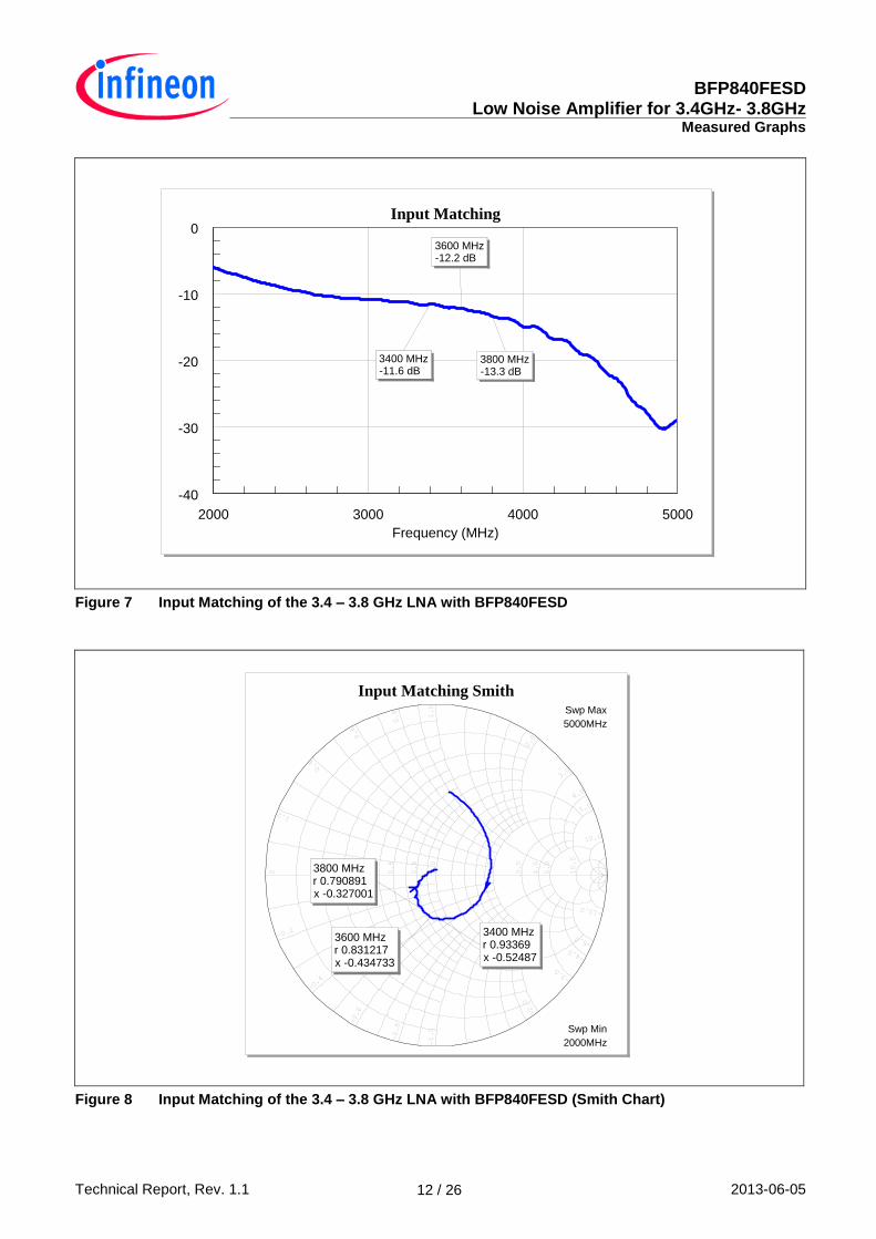
3800 MHz-13.3 dB
3600 MHz-12.2 dB
3400 MHz-11.6 dB
Figure 7 Input Matching of the 3.4 – 3.8 GHz LNA with BFP840FESD
0 1.0
1.0
-1.0
10.0
10.0
-10.0
5.0
5.0
-5.0
2.0
2.0
-2.0
3.0
3.0
-3.0
4.0
4.0
-4.0
0.2
0.2
-0.2
0.4
0.4
-0.4
0.6
0.6
-0.6
0.8
0.8
-0.8
Input Matching SmithSwp Max
5000MHz
Swp Min
2000MHz
3800 MHzr 0.790891x -0.327001
3600 MHzr 0.831217x -0.434733
3400 MHzr 0.93369x -0.52487
Figure 8 Input Matching of the 3.4 – 3.8 GHz LNA with BFP840FESD (Smith Chart)

BFP840FESD
Low Noise Amplifier for 3.4GHz- 3.8GHz Measured Graphs
Technical Report, Rev. 1.1 2013-06-05 13 / 26
2000 3000 4000 5000
Frequency (MHz)
Output Matching
-40
-30
-20
-10
0
3400 MHz-23.8 dB
3600 MHz-23.7 dB
3800 MHz-15 dB
Figure 9 Output Matching of the 3.4 – 3.8 GHz LNA with BFP840FESD
0 1.0
1.0
-1.0
10.0
10.0
-10.0
5.0
5.0
-5.0
2.0
2.0
-2.0
3.0
3.0
-3.0
4.0
4.0
-4.0
0.2
0.2
-0.2
0.4
0.4
-0.4
0.6
0.6
-0.6
0.8
0.8
-0.8
Output Matching SmithSwp Max
5000MHz
Swp Min
2000MHz
3800 MHzr 1.36842x 0.198658
3400 MHzr 0.965828x -0.12063
3600 MHzr 1.13344x 0.0318644
Figure 10 Output Matching of the 3.4 – 3.8 GHz LNA with BFP840FESD (Smith Chart)

BFP840FESD
Low Noise Amplifier for 3.4GHz- 3.8GHz Measured Graphs
Technical Report, Rev. 1.1 2013-06-05 14 / 26
100 5100 10100 15000
Frequency (MHz)
Stability k Factor
0
0.5
1
1.5
2
2.5
3
10081 MHz1.3
Figure 11 Wideband Stability k Factor of the 3.4 – 3.8 GHz LNA with BFP840FESD
10 5010 10010 15000
Frequency (MHz)
Stability Mu Factor
0
1
2
3
4MU1 MU2
Figure 12 Wideband Stability Mu Factor of the 3.4 – 3.8 GHz LNA with BFP840FESD

BFP840FESD
Low Noise Amplifier for 3.4GHz- 3.8GHz Measured Graphs
Technical Report, Rev. 1.1 2013-06-05 15 / 26
-25 -20 -15 -10 -5 0
Pin (dBm)
Input 1dB Compression Point_3G6
0
5
10
15
20
25
Ga
in(d
B)
-25 dBm17.78 dB
-12.6 dBm16.78 dB
Figure 13 1dB Compression Point of the BFP840FESD Circuit at 3600 MHz
3598 3599 3600 3601 3602 3603
Frequency (MHz)
Output 3rd Order Intercept Point_3G6
-100
-80
-60
-40
-20
0
Pow
er
(dB
m)
3601 MHz-20.1
3599 MHz-87.9
3600 MHz-20.1
3602 MHz-89.7
Figure 14 Output 3rd
Order Intercept Point of BFP840FESD at 3600 MHz

BFP840FESD
Low Noise Amplifier for 3.4GHz- 3.8GHz Measured Graphs
Technical Report, Rev. 1.1 2013-06-05 16 / 26
1000 3000 5000 7000 9000 10000
Frequency (MHz)
OFF_Mode
-100
-80
-60
-40
-20
0
3400 MHz-25.1 dB
3600 MHz-24.8 dB
3800 MHz-24.7 dB
Figure 15 OFF-Mode (Vcc = 0V, Icc = 0mA) S21 of the 3.4 – 3.8 GHz LNA with BFP840FESD
1000 3000 5000 7000 9000 10000
Frequency (MHz)
OFF_Mode
-100
-80
-60
-40
-20
0
3400 MHz-25.1 dB
3600 MHz-24.8 dB
3800 MHz-24.7 dB
Figure 16 OFF-Mode (Vcc = 0V, Icc = 0mA) S21 of the 3.4 – 3.8 GHz LNA with BFP840FESD

BFP840FESD
Low Noise Amplifier for 3.4GHz- 3.8GHz Measured Graphs
Technical Report, Rev. 1.1 2013-06-05 17 / 26
-40 -15 10 35 60 85
Temperature (DegC)
Bias Current
10
12
14
16
18
20
Icc (
mA
)
25 DegC14.6
85 DegC12
-40 DegC16.8
PlotCol(1,2)Bias_current
Figure 17 Bias current in the Temperature Range from -40˚C to 85˚C (Vcc=3.0 V)
3.4 3.5 3.6 3.7 3.8
Frequency (GHz)
Noise Figure
0.6
0.7
0.8
0.9
1
1.1
1.2
1.3
1.4
1.5
NF
(d
B)
-40 °C 0 °C 25 °C 50 °C 85 °C
Figure 18 Noise Figure of BFP840FESD LNA in the Temperature Range from -40˚C to 85˚C (Vcc=3.0V)

BFP840FESD
Low Noise Amplifier for 3.4GHz- 3.8GHz Measured Graphs
Technical Report, Rev. 1.1 2013-06-05 18 / 26
2 2.5 3 3.5 4 4.5 5
Frequency (GHz)
10
12
14
16
18
20
22
S21 (
dB
)
3.8 GHz17.83 dB
3.4 GHz18.9 dB
3.8 GHz16.4 dB
3.4 GHz17.38 dB
-40 °C 0 °C 25 °C 50 °C 85 °C
Figure 19 BFP840FESD LNA Insertion Power Gain in the Temperature Range from -40˚C to 85˚C
(Vcc=3.0 V)
3.2 3.4 3.6 3.8 4
Frequency (GHz)
-35
-33
-31
-29
-27
-25
S12 (
dB
)
-40 °C 0 °C 25 °C 50 °C 85 °C
Figure 20 BFP840FESD LNA Reverse Isolation in the Temperature Range from -40˚C to 85˚C
(Vcc=3.0V)

BFP840FESD
Low Noise Amplifier for 3.4GHz- 3.8GHz Measured Graphs
Technical Report, Rev. 1.1 2013-06-05 19 / 26
2.5 3 3.5 4 4.5 5 5.5 6
Frequency (GHz)
-40
-30
-20
-10
0
S11 (
dB
)
3.8 GHz-15.58 dB
3.4 GHz-12.81 dB
3.8 GHz-11.64 dB
3.4 GHz-9.963 dB
-40 °C 0 °C 25 °C 50 °C 85 °C
Figure 21 BFP840FESD LNA Input Matching in the Temperature Range from -40˚C to 85˚C (Vcc=3.0 V)
0 1.0
1.0
-1.0
10.0
10.0
-10.0
5.0
5.0
-5.0
2.0
2.0
-2.0
3.0
3.0
-3.0
4.0
4.0
-4.0
0.2
0.2
-0.2
0.4
0.4
-0.4
0.6
0.6
-0.6
0.8
0.8
-0.8
S11Swp Max
4GHz
Swp Min
3.2GHz
-40 °C 0 °C 25 °C 50 °C 85 °C
Figure 22 BFP840FESD LNA Input Matching in the Temperature Range from -40˚C to 85˚C (Smith
Chart) (Vcc=3.0 V)

BFP840FESD
Low Noise Amplifier for 3.4GHz- 3.8GHz Measured Graphs
Technical Report, Rev. 1.1 2013-06-05 20 / 26
2.5 3 3.5 4 4.5 5 5.5 6
Frequency (GHz)
-50
-40
-30
-20
-10
0
10
S2
2 (
dB
)
3.8 GHz-12.79 dB
3.4 GHz-27.93 dB
-40 °C 0 °C 25 °C 50 °C 85 °C
Figure 23 BFP840FESD LNA Output Matching in the Temperature Range from -40˚C to 85˚C
(Vcc=3.0V)
0 1.0
1.0
-1.0
10.0
10.0
-10.0
5.0
5.0
-5.0
2.0
2.0
-2.0
3.0
3.0
-3.0
4.0
4.0
-4.0
0.2
0.2
-0.2
0.4
0.4
-0.4
0.6
0.6
-0.6
0.8
0.8
-0.8
S22Swp Max
4GHz
Swp Min
3.2GHz
-40 °C 0 °C 25 °C 50 °C 85 °C
Figure 24 BFP840FESD LNA Output Matching in the temperature range from -40 ˚C to 85 ˚C (Smith
Chart) (Vcc=3.0 V)

BFP840FESD
Low Noise Amplifier for 3.4GHz- 3.8GHz Measured Graphs
Technical Report, Rev. 1.1 2013-06-05 21 / 26
-20 -18 -16 -14 -12 -10 -8
Input power (dBm)
12
14
16
18
20
Outp
ut pow
er
(dB
m)
-20 dBm18.263
-20 dBm16.808
-12.84 dBm15.8
-12.91 dBm17.26
-40 °C 0 °C 25 °C 50 °C 85 °C
Figure 25 1dB Compression Point of the BFP840FESD LNA at 3.6 GHz in the Temperature Range from
-40˚C to 85˚C (Vcc=3.0 V)
0.2 5.2 10.2 15
Frequency (GHz)
K factor
0
1
2
3
4
5
10.18 GHz1.117
-40 °C 0 °C 25 °C 50 °C 85 °C
Figure 26 K Factor of the BFP840FESD LNA in the Temperature Range from -40˚C to 85˚C (Vcc=3.0 V)

BFP840FESD
Low Noise Amplifier for 3.4GHz- 3.8GHz Measured Graphs
Technical Report, Rev. 1.1 2013-06-05 22 / 26
0.01 5.01 10.01 15
Frequency (GHz)
u1
0
1
2
3
4
-40 °C 0 °C 25 °C 50 °C 85 °C
Figure 27 µ1 Factor of the BFP840FESD LNA in the Temperature Range from -40˚C to 85˚C (Vcc=3.0 V)
0.05 5.05 10.05 15
Frequency (GHz)
u2
0
1
2
3
4
-40 °C 0 °C 25 °C 50 °C 85 °C
Figure 28 µ2 Factor of the BFP840FESD LNA in the Temperature Range from -40˚C to 85˚C (Vcc=3.0 V)

BFP840FESD
Low Noise Amplifier for 3.4GHz- 3.8GHz Evaluation Board and layout Information
Technical Report, Rev. 1.1 2013-06-05 23 / 26
3 Evaluation Board and layout Information
In this Technical Report, the following PCB is used:
PCB Marking: M13031106 0.6mmEDG TSFP-4-1 BFP840FESD
PCB Board Material: Standard FR4
ᵋr of PCB Material: 4.3 (FR4)
Figure 29 Photo Picture of Evaluation Board
Figure 30 Zoom-In Picture of the BFP840FESD 3.4 – 3.8 GHz LNA Evaluation Board

BFP840FESD
Low Noise Amplifier for 3.4GHz- 3.8GHz Evaluation Board and layout Information
Technical Report, Rev. 1.1 2013-06-05 24 / 26
0.3mm
0.6mm
BFP840FESD
Figure 31 Layout Proposal for RF Grounding of the 3.4 – 3.8 GHz LNA with BFP840FESD
Figure 32 PCB Layer Information
Copper
35µm
FR4 Core, 0.2 mm
FR4 Prepreg,
0.8 mm
Vias

BFP840FESD
Low Noise Amplifier for 3.4GHz- 3.8GHz Authors
Technical Report, Rev. 1.1 2013-06-05 25 / 26
4 Authors
Shamsuddin Ahmed, Application Engineer of Business Unit “RF and Protection Devices” Fang Jie, Application Engineer of Business Unit “RF and Protection Devices”

w w w . i n f i n e o n . c o m
Published by Infineon Technologies AG TR1129

![C-Band Power Amplifier MMIC 900 1100 1300 1500 1700 1900 2100 2300 Drain Current [mA] IDD(DC)=700mA 1100mA 1500mA @f=3.4GHz, VDD=6V 18 20 22 24 26 28 30 32 34 36-10 -8 -6 -4 -2 0 2](https://static.fdocuments.us/doc/165x107/612f072c1ecc515869432ec3/c-band-power-amplifier-mmic-900-1100-1300-1500-1700-1900-2100-2300-drain-current.jpg)