Benchtop Molecular Printer -...
16
Benchtop Molecular Printer Nano eNabler System TM “The possible applications are limited only by one’s imagination” Jan Hoh Ph.D. Johns Hopkins University School of Medicine
Transcript of Benchtop Molecular Printer -...

Benchtop Molecular PrinterNano eNabler SystemTM
“The possible applications are limited only by one’s imagination”
Jan Hoh Ph.D.Johns Hopkins University School of Medicine
BioForce Nano eNabler ™ System
noit amr of ni er o
m r of moc. onanecr of oi b.
ww
w ti si v
Antibodies and other proteins
Nucleic acidsVirusesAdhesivesColloidal particlesQuantum dotsEtchants, solvents
Biosensors, biomedical devices, molecularscreening, cell biology, nanobiologyGene chips, genomiBiosensors, diagnostics, nanodevicesMEMS, nanodevicesElectronics, nanodevices, materials R&DOptical devices, diagnostics, materials R&DMEMS, electronics, microfabrication
cs R&D, biosensors
Material Deposited Representative Applications
The Nano eNabler™ system is a new and enabling technology for ultramicro- and nanoscale fluid delivery. It is a multi-faceted platform capable of delivering attoliter to femtoliter (10-15 to 10-18 liter) volumes of solutions containing biomolecules and other materials to defined locations on surfaces with ultramicro (1-20 µm) feature sizes and nanometer spatial resolution. The ultraminiaturized nature of this technology reduces sample requirements to a bare minimum. For example, the Nano eNabler printer can create a diagnostic biochip that uses just a few cells, or less than one drop of blood, for critical biomedical analysis. The broad applicability and wide range of compatible materials create many new and exciting opportu-nities. A few representative examples of printable materials and their applications may be found in the table below.
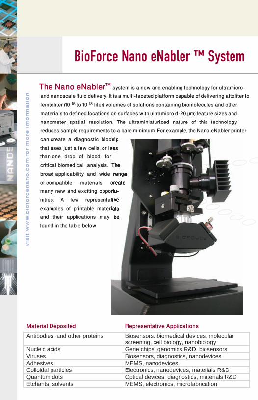
Specifications:
Silicon, GlassGold, Other MetalsAlkanethiol MonolayersSilanes
PDMSHydrogelsNitrocellulosePlastics and Other Polymers
� Power Requirements: AC 120V/60Hz 4.0A AC 240V/50Hz 2.0A� Dimensions: 51 cm x 37 cm x 33 cm� Controller Dimensions: 54 cm x 54 cm x 64 cm� Instrument Weight: 18.14 kg (40 lb)� Controller Weight: 38.6 kg (85 lb)� X,Y Stage Travel Range: 50 mm x 50 mm� X,Y Stage Resolution: 20 nm� Z Stage Range: 45 mm� Z Stage Fine Resolution: 100 nm� Laser-Based Force Feedback� Controllable Humidity Range: 25 - 80% RH� Motorized Optical Microscope (150X to 1000X) w/ Video Capture� Integrated Pentium 4 3.0GHz, 512MB RAM� Windows XP Professional� Flat Screen LCD Monitor
� Partial List of Compatible Surfaces:

The FEMTO Process
“The versatility of this method makes it a powerful tool for nearly any lab.”
noit amr of ni er o
m r of moc. onanecr of oi b.
ww
w ti si v
(a.) (b.) (c.)
The FEMTO process enables the direct deposition of virtually any molecule onto virtually any surface. Small molecules, biomol-ecules, reactive solutions, and even nanoparticles can be printed onto a surface. In fact, because this is a fluid transfer, the size or molecular weight of the material has no effect on the process. Rapidly print thousands of spots with attoliter to femtoliter volumes and diameters from 1-20 microns. Need to draw lines instead? FEMTO’s continuous fluid flow can handle that too.
The key to the FEMTO process is the surface patterning tool (SPTTM), with its microfluidic channels constantly delivering a fresh supply of liquid to be transferred onto the surface. Multi-channel SPTs can be easily loaded to allow parallel printing of a single compound, or multiplexed printing of several different molecules.
As depicted in the illustration below, fluid flows from the reservoir, down the channel, to the end of the cantilever where the channel narrows to a tiny gap (a). Upon contact with the surface, a small volume of liquid held in the gap by surface tension is directly transferred to the surface in an event typically requiring less than 100 msec (b). Capillary fluid flow down the channel instantly replen-ishes the volume at the gap, and the SPT is ready to print the next feature (c).
Fluidics Enhanced Molecular Transfer Operation
The FEMTO Process
How is FEMTO Different from Other Methods?
FEMTO DPN Nanopipettes µCP
Parallel Printing
Multiplexing
Rapid Revisions
Versatility
Speed
Small Molecules
Large Molecules
Reliability
�
�
�
�
�
�
�
�
�
�
�
�
�
�
�
�
Each method of surface modification has its own set of advantages and disad-vantages. PDMS microcontact printing (µCP) may offer the benefit of parallel printing but at the cost of other very useful features such as multiplexing and the flexibility of on-the-fly revisions. A scanning probe method such as Dip Pen Nanolithography (DPN) is a good choice for creating very small features of a low molecular weight compound, however this technique has drawbacks as well. DPN is a diffusion-limited process, which means the printing speed for larger spots and higher M.W. molecules such as proteins can be very slow. Other common complaints from DPN users include a limited selection of suitable surfaces and a lack of reproducibility. Techniques employing glass nanopipettes offer the speed of a direct fluid flow process such as FEMTO, but the nanopipettes can be difficult to load and their closed design makes them prone to blockage. FEMTO’s open channels ensure that your liquid will always have a path to the surface for maximum reliability.
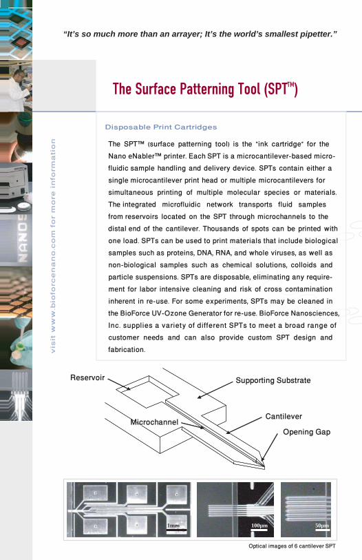
The Surface Patterning Tool (SPTTM)
“It’s so much more than an arrayer; It’s the world’s smallest pipetter.”
Optical images of 6 cantilever SPT
100µm1mm 50µm
noit amr of ni er o
m r of moc. onanecr of oi b.
ww
w ti si v
Mic
Reservoir
MicrochannelOpening Gap
Cantilever
Supporting Substrate
The SPT™ (surface patterning tool) is the “ink cartridge” for the Nano eNabler™ printer. Each SPT is a microcantilever-based micro-fluidic sample handling and delivery device. SPTs contain either a single microcantilever print head or multiple microcantilevers for simultaneous printing of multiple molecular species or materials. The integrated microfluidic network transports fluid samples from reservoirs located on the SPT through microchannels to the distal end of the cantilever. Thousands of spots can be printed with one load. SPTs can be used to print materials that include biological samples such as proteins, DNA, RNA, and whole viruses, as well as non-biological samples such as chemical solutions, colloids and particle suspensions. SPTs are disposable, eliminating any require-ment for labor intensive cleaning and risk of cross contamination inherent in re-use. For some experiments, SPTs may be cleaned in the BioForce UV-Ozone Generator for re-use. BioForce Nanosciences, Inc. supplies a variety of different SPTs to meet a broad range of customer needs and can also provide custom SPT design and fabrication.
Disposable Print Cartridges
The Surface Patterning Tool (SPTTM)For creating arrays of biomolecules, the preferred method of loading the deposi-tion tool will depend upon the ultimate density of the nanoarray. Arrays of a single compound can be created using either front loading or back loading of the deposition tool.
Back LoadingBack loading involves pipetting a small volume (generally less than 0.5 µl) of sample into one of the wells etched into the top surface of the silicon deposition tool substrate. The sample will fill the well and flood the channel that runs down the length of the cantilever. Several thousand features may be printed with a back-filled SPT.
Front LoadingFront loading of SPTs is often convenient for arraying compounds in a relatively small number of domains (100s). The solution of interest is placed on a coverslip or similar surface (far less than 1 µl is required). The user then mounts the loading slide or coverslip onto the Nano eNabler™ sample platform. The SPT is positioned above the loading spot. The Nano eNabler system’s “Find Surface” command is then used to bring the deposition tool and loading surface into contact. Finally, the precision X,Y control of the Nano eNabler system is used to touch the SPT to the solution of interest, and spontaneously fill the SPT micro-channel.

The Surface Patterning Tool (SPTTM)
“It’s so much more than an arrayer; It’s the world’s smallest pipetter.”
Optical images of 6 cantilever SPT
100µm1mm 50µm
n oitamrofni ero
m rof mo c.o n a n e crofoib.
ww
w tisiv
Mic
Reservoir
MicrochannelOpening Gap
Cantilever
Supporting Substrate
The SPT™ (surface patterning tool) is the “ink cartridge” for the Nano eNabler™ printer. Each SPT is a microcantilever-based micro-fluidic sample handling and delivery device. SPTs contain either a single microcantilever print head or multiple microcantilevers for simultaneous printing of multiple molecular species or materials. The integrated microfluidic network transports fluid samples from reservoirs located on the SPT through microchannels to the distal end of the cantilever. Thousands of spots can be printed with one load. SPTs can be used to print materials that include biological samples such as proteins, DNA, RNA, and whole viruses, as well as non-biological samples such as chemical solutions, colloids and particle suspensions. SPTs are disposable, eliminating any require-ment for labor intensive cleaning and risk of cross contamination inherent in re-use. For some experiments, SPTs may be cleaned in the BioForce UV-Ozone Generator for re-use. BioForce Nanosciences, Inc. supplies a variety of different SPTs to meet a broad range of customer needs and can also provide custom SPT design and fabrication.
Disposable Print Cartridges
The Surface Patterning Tool (SPTTM)For creating arrays of biomolecules, the preferred method of loading the deposi-tion tool will depend upon the ultimate density of the nanoarray. Arrays of a single compound can be created using either front loading or back loading of the deposition tool.
Back LoadingBack loading involves pipetting a small volume (generally less than 0.5 µl) of sample into one of the wells etched into the top surface of the silicon deposition tool substrate. The sample will fill the well and flood the channel that runs down the length of the cantilever. Several thousand features may be printed with a back-filled SPT.
Front LoadingFront loading of SPTs is often convenient for arraying compounds in a relatively small number of domains (100s). The solution of interest is placed on a coverslip or similar surface (far less than 1 µl is required). The user then mounts the loading slide or coverslip onto the Nano eNabler™ sample platform. The SPT is positioned above the loading spot. The Nano eNabler system’s “Find Surface” command is then used to bring the deposition tool and loading surface into contact. Finally, the precision X,Y control of the Nano eNabler system is used to touch the SPT to the solution of interest, and spontaneously fill the SPT micro-channel.
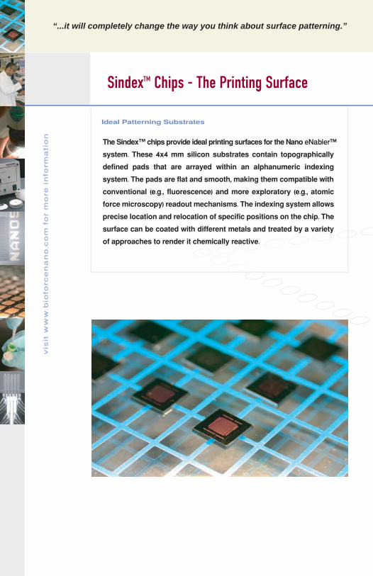
SindexTM Chips - The Printing Surface
Ideal Patterning Substrates
“...it will completely change the way you think about surface patterning.”
noit amr of ni er o
m r of moc. onanecr of oi b.
ww
w ti si v
The Sindex™ chips provide ideal printing surfaces for the Nano eNabler™system. These 4x4 mm silicon substrates contain topographically defined pads that are arrayed within an alphanumeric indexing system. The pads are flat and smooth, making them compatible with conventional (e.g., fluorescence) and more exploratory (e.g., atomic force microscopy) readout mechanisms. The indexing system allows precise location and relocation of specific positions on the chip. The surface can be coated with different metals and treated by a variety of approaches to render it chemically reactive.
Chip Type Array No. Pad sizeµm
Spacingµm nm
Etch depth Chipsize,mm
Chip thickness,µm
Material
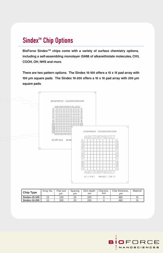
Sindex-15-100 15 100 20 200 4 480 SiSindex-10-200 10 200 20 200 4 480 Si
SindexTM Chip OptionsBioForce Sindex™ chips come with a variety of surface chemistry options, including a self-assembling monolayer (SAM) of alkanethiolate molecules; CH3, COOH, OH, NHS and more.
There are two pattern options. The Sindex 15-100 offers a 15 x 15 pad array with 100 µm square pads. The Sindex 10-200 offers a 10 x 10 pad array with 200 µm square pads.
SindexTM Chips - The Printing Surface
Ideal Patterning Substrates
“...it will completely change the way you think about surface patterning.”
n oitamrofni ero
m rof mo c.o n a n e crofoib.
ww
w ti siv
The Sindex™ chips provide ideal printing surfaces for the Nano eNabler™system. These 4x4 mm silicon substrates contain topographically defined pads that are arrayed within an alphanumeric indexing system. The pads are flat and smooth, making them compatible with conventional (e.g., fluorescence) and more exploratory (e.g., atomic force microscopy) readout mechanisms. The indexing system allows precise location and relocation of specific positions on the chip. The surface can be coated with different metals and treated by a variety of approaches to render it chemically reactive.
Chip Type Array No. Pad sizeµm
Spacingµm nm
Etch depth Chipsize,mm
Chip thickness,µm
Material
Sindex-15-100 15 100 20 200 4 480 SiSindex-10-200 10 200 20 200 4 480 Si
SindexTM Chip OptionsBioForce Sindex™ chips come with a variety of surface chemistry options, including a self-assembling monolayer (SAM) of alkanethiolate molecules; CH3, COOH, OH, NHS and more.
There are two pattern options. The Sindex 15-100 offers a 15 x 15 pad array with 100 µm square pads. The Sindex 10-200 offers a 10 x 10 pad array with 200 µm square pads.

Software Interface
The Nano eNabler™ system utilizes Windows™ based BioForce authored software that allows the user to control nearly every aspect of the instrument. The modular nature of the software creates oppor-tunities for rapid creation of user-specific functions.
Flexible Software Interface
“It is an incredibly exciting platform for patterning molecules.”
noit amr of ni er o
m r of moc. onanecr of oi b.
ww
w ti si v
Software Controlled:� X,Y Movement� Z Movement� Optical Focus and Zoom� Optical Illumination� Laser Intensity� Environmental Control� Integrated Video
Features:� Design & Spot Complex Pattern Layouts on the Fly� Save Load & Deposition Locations, Pattern Layouts� Definable Dwell & Wait Time for Spot Size Optimization� Multi-Chip Automated Arraying� Automatic Find Surface� Contact Force Modes:
� Automatic Contact Force� Manual Contact Force Value� No Laser Feedback
� Save Video/Photos from Integrated Video� On Video X,Y,Z Navigation

Screenshot of Nano eNabler Software Interface
Easily design and save complex pattern layouts, adjust column
and row separation
Optimize spot size by adjusting contact force, dwell time, wait time, and withdraw distance

Environmental Control
Humidity is one of the most important variables to control when attempting to print micron or sub-micron scale features. Insufficient humidity can negatively impact material transfer, and excessive humidity can results in undesirable heterogeneity of feature size. The Nano eNabler™ system is equipped with an outer enclosure that provides a barrier between the Nano eNabler™ instrumentation and the ambient room conditions.
Precise Control for Patterning Optimization
“The Nano eNabler is one of those new tools that come along infrequently...”
noit amr of ni er o
m r of moc. onanecr of oi b.
ww
w ti si v
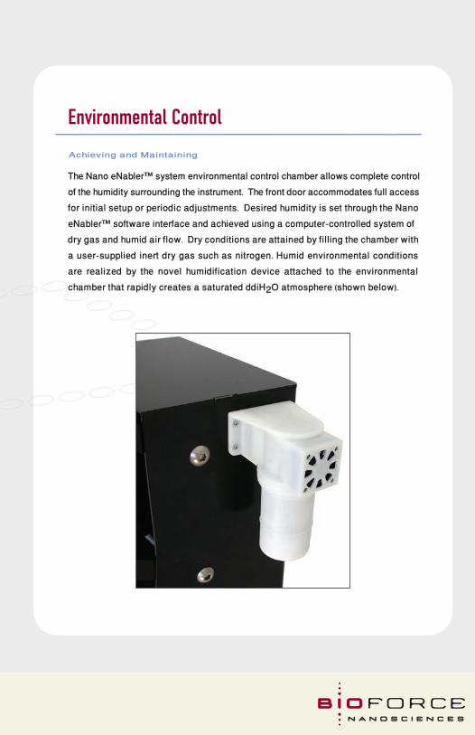
Environmental Control
Achieving and Maintaining
The Nano eNabler™ system environmental control chamber allows complete controlof the humidity surrounding the instrument. The front door accommodates full access for initial setup or periodic adjustments. Desired humidity is set through the Nano eNabler™ software interface and achieved using a computer-controlled system of dry gas and humid air flow. Dry conditions are attained by filling the chamber with a user-supplied inert dry gas such as nitrogen. Humid environmental conditions are realized by the novel humidification device attached to the environmental chamber that rapidly creates a saturated ddiH2O atmosphere (shown below).

Applications
“It is an innovative instrument for various surface science technologies.”
noit amr of ni er o
m r of moc. onanecr of oi b.
ww
w ti si v
Additional Applications:� Molecular Detection � Chemical and Biosensor Functionalization � Cantilever Sensors � Nanotube Sensors � Optical Waveguide Sensors � Printing Inside Microfluidic Channels
� Diagnostics and Pharmaceutical Discovery � Small Volume Biomarker Analysis � Laser Capture Microdissection Samples � Single Cell Expression Profiling � Small Animal/Organism Model Systems � Pre-Natal Biomarker Screening � Patterning Surfaces for Cellular Studies � Stem Cell Differentiation/Proliferation � Cell Adhesion/Motility/Chemotaxis � Tissue Engineering � Peptide/MHC Complexes
� Engineering Surface Architectures � Direct Patterning of Nanomaterials � Quantum Dots, Colloids, Magnetic Nanoparticles
� Patterning Reactive Solutions � Etchants, Resists, Adhesives
Application Notes
The ability of the Nano eNablerTM system to deliver attoliter volumes of materials to defined locations with nanoscale accuracy creates an unprecedented opportunity for discovery science. The open-ended possibilities enabled by the Nano eNabler platform are rapidly being documented in a series of application notes (available at www.bioforcenano.com). Each application note describes a use of the Nano eNabler system developed either in-house, or by our growing user base. Some examples appear at the right.

Patterning Nanomaterials
Protein-Protein InteractionScreening by AFM
ViriChipTM - Virus Detection by AFM
3 nm 6 nm
Rabbit anti-HBsAg + anti-Rabbit IgG
Drawing lines and printing patterns with quantum dots
A novel biosensor platform enabled by the Nano eNablerTM platform.
The ultraminiaturized size of patterns made by the Nano eNablerTM printer, enable the use of novel approaches to identify molecular interac-
tions. Here the AFM is used to evalu-ate a 4 x 4 array of antibody-antigen interaction domains on a biochip surface.
Image courtesy of J. Hoh, Johns Hopkins University
Patterning for Protein-Cell StudiesSpots or lines of extracellular matrix proteins or cell signalling molecules can be patterned to enable the study of single cells. Complex patterns of multiple proteins may be constructed such that a single cell interacts with many spots.

noit amrof ni ero
m rof moc. onanecrof oi b.
ww
w ti si v
1615 Golden Aspen Drive, Suite 101 • Ames, IA 50010 USA
Phone: 515.233.8333 • Fax: 515.233.8337www.bioforcenano.com • Email: [email protected] Symbol: BFNH.OB
Nano eNabler is a trademark of BioForce Nanosciences.All other trademarks are property of their respective owners.