
Behaviour of
179
Coupling of Electromagnetic Fields from Intentional High Power Electromagnetic Sources with a Buried Cable and an Airborne Vehicle in Flight A Thesis Submitted for the Degree of Doctor of Philosophy in the Faculty of Engineering By Sunitha K Department of Electrical Engineering Indian Institute of Science Bangalore - 560 012 India September 2012
-
Upload
sadie-williamson -
Category
Documents
-
view
23 -
download
9
Transcript of Behaviour of

Coupling of Electromagnetic Fields from
Intentional High Power Electromagnetic
Sources with a Buried Cable and an
Airborne Vehicle in Flight
A Thesis
Submitted for the Degree of
Doctor of Philosophyin the Faculty of Engineering
By
Sunitha K
Department of Electrical Engineering
Indian Institute of Science
Bangalore - 560 012
India
September 2012

Acknowledgements
I consider this acknowledgement as one of the few opportunities in life when I get to reflect
back on my actions and realize the contributions of those people who have made a tremendous
impact in all my endeavors. I believe this thesis is not just about getting a doctorate degree,
but it contains the guidance, encouragement, motivation, advice and blessings of several
people and everytime I open this thesis, I would have the greatest pride to have interacted
with such wonderful people at some point of time.
Today, I find immense pleasure in extending my heartfelt gratitude and sincere thanks
to all of you who have made this thesis possible.
At the forefront, I would like to express my deepest gratitude to my research supervisor,
Dr. Joy Thomas M. for his willingness to consider me as his student and more importantly
for agreeing to pursue research on the present topic . I would remain indebted to him for
the amount of efforts and time he had spent all these years in trying to generate research
facilities to pursue this research work and also for his patient hearing to all associated
problems. His nature of being more of a friend rather than a supervisor has always provided
extra energy in my research efforts. I would always cherish the valuable time spent with
him over long discussions related to both research and non-research interests. His constant
encouragement, continuous support and help during the duration of my stay in IISc have
always been a tremendous source of motivation for me. Thank You, Sir for everything you
did for me.
When I write this acknowledgement, I cannot forget Dr.D.V.Giri, Protech, Alamo, CA
who had helped me through out my research work and had given valuable suggestions for
improving the quality of the work. Besides my research supervisor, he had extended me all
his support and shared all his experiences and knowledge in the area of my research topic.
This had given me lot of insight to the problem at hand and was able to do the computations.
i

ii Acknowledgements
My experimental work would not have been complete without the timely help and co-
operation extended by Mr. Riaz Ahmed, Mr. Sreedharan in the High Voltage Laboratory,
Dept. of Electrical Engineering, IISc and my special thanks goes to them.
I would like to thank the Indian Institute of Science for providing me the Institute
scholarship, the facility to stay in its beautiful campus and for the technical facilities to
pursue this research work. My sincere thanks are due to Dr.P.S.Sastry for extending the
necessary facilities in the department when he was the Chairman of the department and for
his support towards my other interests.
I do not know how to thank to all my labmates, Mr. Sisir, Mr. Venkatesulu, Mr. Sridhar
Preetha P., Joseph and who were always available to help me during my presentations in the
laboratory and also in times of need. I am going to miss you all and also the lively technical
discussions we usually have in the laboratory. Thank you so much for everything.
I am very thankful to my very dear friends, for their support and encouragement over all
these years.
Words can not help me in expressing my deep sense of gratitude to my mother, my in
laws and my husband and my daughter for their constant encouragement and moral support
throughout my research work. I will remain forever indebted to them for giving me the
support.
THANK YOU ALL
Sunitha K
Abstract
Society’s dependence on electronic and electrical systems has increased rapidly over the past
few decades, and people are relying more and more on these gadgets in their daily life because
of the efficiency in operation which these systems can offer. This has revolutionized many
areas of electrical and electronics engineering including power sector, telecommunication
sector, transportation and many other allied areas. With progress in time, the sophistication
in the systems also increased. Also as the systems size reduced from micro level to nano
level, the compactness of the system also increased. This paved the way for development in
the digital electronics leading to new and efficient ICs that came into existence. Power sector
also faced a resurge in its technology. Most of the analog meters are now replaced by digital
meters. The increased sophistication and compactness in the digital system technology made
it susceptible to electromagnetic interference especially from High Power Electromagnetic
Sources. Communication, data processing, sensors, and similar electronic devices are vital
parts of the modern technological environment. Damage or failures in these devices could
lead to technical or financial disasters as well as injuries or the loss of life.
Electromagnetic Interference (EMI) can be explained as any malicious generation of
electromagnetic energy introducing noise or signals into electric and electronic systems, thus
disrupting, confusing or damaging these systems. The disturbance may interrupt, obstruct,
or otherwise degrade or limit the effective performance of the circuit. These effects can range
from a simple degradation of data to a total loss of data. The source may be any object, arti-
ficial or natural, that carries rapidly changing electrical currents, such as an electrical circuit.
The sources of electromagnetic interference can be either unintentional or intentional. The
sources producing electromagnetic interference can be of different power levels,different fre-
quency of operation and of different field strength.One such classification of these sources are
the High Power Electromagnetic Sources (HPEM) High Power Electromagnetic environment
iii

iv Abstract
refers to sources producing very high peak electromagnetic fields at very high power levels.
These power levels coupled with the extremely high magnitude of the fields are sufficient
to cause disastrous effects on the electrical and electronic systems. There has been a lot of
developments in the field of the source technology of HPEM sources so that they are now
one of the strongest sources of electromagnetic interference.
High Power Electromagnetic environment refers to the sources producing very high peak
electromagnetic fields at very high power levels. These power levels coupled with the ex-
tremely high magnitude of the fields are sufficient to cause disastrous effects on the electrical
and electronic systems. HPEM environments are categorized based on the source char-
acteristics such as the peak electric field, often called threat level, frequency coverage or
bandwidth, average power density and energy content. The sources of electromagnetic inter-
ference can be either unintentional or intentional. Some examples of unintentional sources
are the increased use of electromagnetic spectrum which generates disturbance to various
systems operating in that frequency band, poor design of systems without taking care of
other systems present nearby as well as lightning. Intentional sources are High altitude
Electromagnetic Pulse (HEMP) or Nuclear Electromagnetic Pulse (NEMP) due to nuclear
detonations, Ultra Wide Band (UWB) field from Impulse Radiating Antennas (IRA), Nar-
row band fields like those coming from High Power Microwaves (HPM), High Intensity Radio
Frequency (HIRF) sources. Of these the lightning is natural and all other sources are man-
made. The significant progress in the Intentional High-Power Electromagnetic (HPEM)
sources and antenna technologies and the easy access to simple HPEM systems for anyone
entail the need to determine the susceptibility of electronic equipment as well as coupling of
these fields with systems such as cables (buried as well as aerial), airborne vehicle etc. to
these types of threats.
Buried cables are widely used in the communication and power sectors due to their effi-
cient functioning in urban cities and towns. These cables are more prone to electromagnetic
interferences from HPEM sources. The buried communication cables or even the buried data
cables are connected to sensitive equipments and hence even a slight rise in the voltage or
the current at the terminals of the equipments can become a serious problem for the smooth
operation of the system. In the first part of the thesis the effect of the electromagnetic field
due to these sources on the cables laid underground has been studied.
The second part of this thesis deals with the study of the interaction of the EM field
from the above mentioned HPEM sources with an airborne vehicle. Airborne vehicle and its
Abstract v
payload are extremely expensive so that any destruction to these as a result of the voltages
and currents induced on the vehicle on account of the incoming HPEM fields can be quite
undesirable. The incoming electromagnetic fields will illuminate the vehicle along its axis
which results in the induction of currents and voltages. These currents and voltages will get
coupled to the internal control circuits that are extremely sensitive. If the induced voltage/
current magnitude happen to be above the damage threshold level of these circuits then it
will result in either a malfunction of the circuit or a permanent damage of it, with both of
them being detrimental to the success of the mission. This will even result in the abortion
of the mission or possible degradation of the vehicle performance. Hence it is worthwhile to
see what will be the influence of an incoming HPEM electromagnetic field on the airborne
vehicle with and without the presence of an exhaust plume.
In this work, the HPEM sources considered are NEMP, IRA and HPM. The electromag-
netic fields produced by the EMP can induce large voltage and current transients in electrical
and electronic circuits which can lead to a possible malfunction or permanent damage of the
systems. The electric field at the earths surface can be modelled as a double exponential
pulse as per the IEC standard 61000-2-9. The NEMP field incident on the earths surface
is considered as that coming from a source at a distance far away from the earths surface;
hence a plane wave approximation has been used. Impulse radiating antennas are the ones
that are used as the major source of ultra wide band radiation. These are highly powerful
antennas that use a pulsed power source as the input and this power source is conditioned
to get an extremely sharp rise time pulse. These antennas are very high power antennas
that are capable of producing a significant electromagnetic field. Impulse radiating antenna
is a paraboloidal reflector and hence is an aperture antenna. Initially the radiated field due
to this aperture needs to be found out at any observation point from the antenna. In this
thesis, the aperture distribution method is used to accurately determine the field due to the
aperture. In this method the field reflected from the surface of the reflector is first found
on an imaginary plane through the focal point of the reflector that is normal to the axis of
the reflector, by using the principles of geometrical optics, which then is extended to the
observation point. The IRA considered for the present work is the one of the most powerful
IRA as per the published literature available in the open domain. This has an input voltage
of 1.025 MV. The far field electric field measured at the boresight (at r =85 m) being equal
to 62 kV/m, and the uncorrected pulse rise time (10%-90%) is 180 ps for this IRA.
HPM sources are usually electromagnetic radiators having a reflector with a horn antenna
vi Abstract
kept at their focal point for excitation. HPM sources generally operate in single mode or at
tens or hundreds of Hz repetition rates. Many HPM radiators are developed in the world
each with their own peculiar geometry and power levels. In the present thesis, a single
waveguide (WR-975) fed HPM antenna assembly has been studied. The chosen waveguide
has a cut-off frequency of 1 GHz and a power level of 10 GW. The wavelength associated
with the waveguide is 0.3 m. The field pattern shows a definite peak in its response when
the frequency is 1GHz, the cut-off frequency of the waveguide.
The electric field coming out of the HPEM sources travel through the medium that is
either air alone or a combination of air and soil respectively depending upon whether the
circuit on which the coupling is analysed is an airborne vehicle or an underground cable.
The media plays a major role in the coupling, as the field magnitude is influenced by the
characteristic properties of the media. As height increases the magnitude of the electric field
decreases for all types of sources and also the time before which the field waveform starts is
increased. The electric field in the soil is decided by the soil properties such as its conductivity
and permittivity. The soil is modelled in such a manner that its conductivity and permittivity
values are taken as a function of frequency by giving due attention to the high frequency
behaviours of soils as the incident field has high frequency components. A soil medium
can be electromagnetically viewed as a four component dielectric mixture consisting of soil
particles, air voids, bound water, and free water. When electric field is incident on the soil,
it gets polarized. This is as a result of a wide variety of processes, including polarization of
electrons in the orbits around atoms, distortion of molecules, reorientation of water molecules,
accumulation of charge at interfaces, and electrochemical reactions. Whatever is the HPEM
source, an increase in the soil conductivity results in an increased attenuation of the field.
Also there is a significant loss of high frequency components in the GHz range in the field
due to the selective absorption by the soil. This effect causes the percentage attenuation
to be maximum for HPM and minimum for NEMP and IRA lying in between these two
extremities. Increase in permittivity of the soil causes attenuation of the electric field for
all HPEM sources. This is due to the relaxation mechanisms in the soil due to atomic- or
molecular-scale resonances.
The coupling of the electromagnetic fields due to HPEM sources is considered in the first
phase. Two cables are considered (i) buried shielded and (ii) buried shielded twisted pair
cables. The results are arrived at using the Enhanced Transmission Line model. The induced
current is more for a shielded cable than a twisted pair cable of the same configuration. The
Abstract vii
induced current magnitude depends upon the type of the HPEM source, the depth of burial
of the cable and the point on the cable where the current/ voltage is computed. Current
is maximum at the centre of the cable for a matched termination and the voltage is the
minimum at this point. The ratio of the induced current in the inner conductor with respect
to the shield current of a shielded cable is the least for an HPM, then comes the IRA and
finally the NEMP. This is due to the fact that higher frequencies are absorbed more by the
shield of the cable. This affects HPM induced current the maximum and NEMP the least
because of the presence of the lower frequency components in NEMP. Induced current in the
twisted pair cable depends upon the number of pairs of the cable and the pitching of the
cable.
The electromagnetic field from the HPEM sources propagates with less attenuation in air
due to the lower resistance this medium offers for electromagnetic wave propagation. Hence
any system in air be it electrical or electronic, will be under the strong illumination by these
electromagnetic fields. As the second part of this thesis, the influence of the electromagnetic
fields from all the three HPEM sources on an airborne vehicle in flight is analysed. For
this part of study, the EM fields radiated by all the three sources at different heights from
the earths surface have been computed. The coupling study has been done for the case of
a vehicle with plume as well as without plume. For the second case, the electromagnetic
modelling of the plume has been done taking into consideration its conductivity, which in turn
depends on the different ionic species present in the plume. The species of the exhaust plume
depends upon the chemical reactions taking place in the combustion chamber of the nozzle of
the vehicle. The presence of the alkali metals as impurity in the airborne vehicle propellant
will generate considerable ion particles such as Na+, Cl− in addition to e- in the plume
mixture during combustion which makes the plume electrically conducting. But it does not
influence the pressure, temperature and velocity of the plume. After the nozzle throat, the
exhaust plume regains the supersonic speed, so the flow of the exhaust plume is assumed
as compressible flow in the second region. The electrons have high collision frequency, high
number density, high plasma frequency and lower molecular mass and hence the highly mobile
electrons dominate the heavy ion particle in the computation of the electrical conductivity of
the plume. The plume conductivity decreases marginally from the axis till a distance equal
to the nozzle radius but the peak value increases sharply towards the exit plane edge of the
nozzle radius. The induced current is computed using Method of Moments. The induced
current depends upon the type of interference source, its characteristics, whether the plume

viii Abstract
is present or not and the type of the plume. The HPM induces maximum current in the
vehicle because of the fact that the plume has a tendency to become more conductive at
these frequencies. The induced currents due to the EM fields from IRA and NEMP comes
after the HPM. The presence of the plume enhances the magnitude of the induced current.
If the plume is homogeneous then the current induced in it is more.

Contents
Acknowledgements i
Abstract iii
Contents xii
List of Tables xiii
List of Figures xiv
1 Introduction 1
1.1 Need for Studying Electromagnetic Interference . . . . . . . . . . . . . . . . 1
1.2 High Power Electromagnetic (HPEM) Environment . . . . . . . . . . . . . . 2
1.3 Failure Rates of Electronic Components due to Electromagnetic Interference 5
1.4 Nuclear Electromagnetic Pulse (NEMP) . . . . . . . . . . . . . . . . . . . . 6
1.4.1 Origin of EMP . . . . . . . . . . . . . . . . . . . . . . . . . . . . . . 7
1.4.2 Classification of EMP Environment . . . . . . . . . . . . . . . . . . . 8
1.4.3 Characteristics of High Altitude EMP . . . . . . . . . . . . . . . . . . 9
1.4.3.1 Spatial Extent . . . . . . . . . . . . . . . . . . . . . . . . . 9
1.4.3.2 Effects of EMP . . . . . . . . . . . . . . . . . . . . . . . . . 10
1.5 Impulse Radiating Antenna (IRA) . . . . . . . . . . . . . . . . . . . . . . . . 12
1.5.1 Primary Energy Storage . . . . . . . . . . . . . . . . . . . . . . . . . 12
1.5.2 Pulse Generator . . . . . . . . . . . . . . . . . . . . . . . . . . . . . . 13
1.5.2.1 Marx Generator [46] . . . . . . . . . . . . . . . . . . . . . . 13
1.5.2.2 Tesla Transformer . . . . . . . . . . . . . . . . . . . . . . . 16
1.5.3 Pulse Sharpening System . . . . . . . . . . . . . . . . . . . . . . . . . 18
ix

x Contents
1.5.4 Antennas . . . . . . . . . . . . . . . . . . . . . . . . . . . . . . . . . 19
1.5.4.1 Paraboloidal Antenna . . . . . . . . . . . . . . . . . . . . . 19
1.5.4.2 Horn Antenna . . . . . . . . . . . . . . . . . . . . . . . . . 19
1.5.4.3 Half IRA . . . . . . . . . . . . . . . . . . . . . . . . . . . . 20
1.5.4.4 Collapsible IRA . . . . . . . . . . . . . . . . . . . . . . . . . 20
1.5.5 Switches . . . . . . . . . . . . . . . . . . . . . . . . . . . . . . . . . . 20
1.5.6 A commercial IRA . . . . . . . . . . . . . . . . . . . . . . . . . . . . 23
1.6 High Power Microwaves (HPM) . . . . . . . . . . . . . . . . . . . . . . . . . 25
1.6.1 Applications of HPM . . . . . . . . . . . . . . . . . . . . . . . . . . . 26
1.7 Objectives of the thesis . . . . . . . . . . . . . . . . . . . . . . . . . . . . . . 26
1.8 Organization of the thesis . . . . . . . . . . . . . . . . . . . . . . . . . . . . 28
2 Electric Field due to Intentional HPEM Sources 30
2.1 Electric Field from a Nuclear Burst . . . . . . . . . . . . . . . . . . . . . . . 30
2.1.1 Polarization and Ground Effects . . . . . . . . . . . . . . . . . . . . . 31
2.1.2 Modelling the NEMP field due to a High Altitude Nuclear Burst . . . 31
2.2 Impulse Radiating Antenna . . . . . . . . . . . . . . . . . . . . . . . . . . . 32
2.2.1 Computation of Radiated Field from an IRA . . . . . . . . . . . . . . 32
2.2.2 Radiation Pattern of IRA in the Near and the Far Field . . . . . . . 37
2.2.3 Illustrative Example in Time Domain . . . . . . . . . . . . . . . . . . 45
2.2.4 Equivalence between Spectral and Temporal Characteristics of IRA . 47
2.3 Electric Field at the Different Points due to a HPM Source . . . . . . . . . . 51
2.4 Chapter Summary . . . . . . . . . . . . . . . . . . . . . . . . . . . . . . . . 54
3 Influence of the Medium on the Electric field Propagation 57
3.1 Electric Field in Different Media due to HPEM Sources . . . . . . . . . . . . 57
3.2 Electric Field in Air at Varied Heights due to HPEM Sources . . . . . . . . . 59
3.3 Electric Field Attenuation due to Soil Characteristics . . . . . . . . . . . . . 61
3.3.1 Effect of Soil Parameters on the Electric Field . . . . . . . . . . . . . 61
3.4 Response of the Soil to the Field Excitation from HPEM Sources . . . . . . 64
3.4.1 Variation of the Conductivity of the Soil on the Response Characteristics 66
3.4.2 Variation of the Permittivity of the Soil on the Electric Field Behaviour 67
Contents xi
3.4.3 Influence of the Depth of Penetration of the Field in the Soil on its
Spectral and Temporal Characteristics . . . . . . . . . . . . . . . . . 69
3.5 Case Study of Typical Types of Soils . . . . . . . . . . . . . . . . . . . . . . 71
3.6 Chapter Summary . . . . . . . . . . . . . . . . . . . . . . . . . . . . . . . . 75
4 Induced Voltage and Current in a Buried Cable due to HPEM Sources 77
4.1 Theory and Background . . . . . . . . . . . . . . . . . . . . . . . . . . . . . 77
4.2 Underground Cable Getting Illuminated by HPEM Sources . . . . . . . . . . 78
4.3 Coupling with the Cable . . . . . . . . . . . . . . . . . . . . . . . . . . . . . 78
4.4 High Frequency Electromagnetic Field Coupling to Buried Cables . . . . . . 81
4.5 Validation of the Proposed Method . . . . . . . . . . . . . . . . . . . . . . . 84
4.6 Induced Voltage/ Current in the Shield of the Cable due to the HPEM Sources 86
4.6.1 Response of the Cable to NEMP Field . . . . . . . . . . . . . . . . . 86
4.6.2 Response of the Cable to an IRA Field . . . . . . . . . . . . . . . . . 87
4.6.3 Response of the Cable to an HPM Field . . . . . . . . . . . . . . . . 90
4.7 Induced Current in Twisted Pair Cable due to HPEM Sources . . . . . . . . 92
4.7.1 Coupling of the EM field due to NEMP with the Twisted Pair Cables 96
4.7.2 Coupling due to IRA Electric Field . . . . . . . . . . . . . . . . . . . 97
4.7.3 Coupling due to HPM Electric Field . . . . . . . . . . . . . . . . . . 103
4.8 Chapter Summary . . . . . . . . . . . . . . . . . . . . . . . . . . . . . . . . 103
5 Coupling of the Field from an HPEM Source with an Airborne Vehicle in
Flight 109
5.1 Introduction . . . . . . . . . . . . . . . . . . . . . . . . . . . . . . . . . . . . 109
5.2 Review of the previous work . . . . . . . . . . . . . . . . . . . . . . . . . . . 110
5.3 Geometry of the Airborne Vehicle . . . . . . . . . . . . . . . . . . . . . . . . 110
5.4 Modeling of the Exhaust Plume . . . . . . . . . . . . . . . . . . . . . . . . . 112
5.5 Electromagnetic Modelling of the Plume . . . . . . . . . . . . . . . . . . . . 113
5.6 Method of analysis used . . . . . . . . . . . . . . . . . . . . . . . . . . . . . 115
5.7 Validation of the Method Used . . . . . . . . . . . . . . . . . . . . . . . . . 120
5.8 Results and Discussions . . . . . . . . . . . . . . . . . . . . . . . . . . . . . 121
5.8.1 Coupling of NEMP with missile . . . . . . . . . . . . . . . . . . . . . 124
5.8.2 Coupling of IRA . . . . . . . . . . . . . . . . . . . . . . . . . . . . . 125

xii Contents
5.8.3 Coupling of HPM . . . . . . . . . . . . . . . . . . . . . . . . . . . . . 131
5.9 Chapter summary . . . . . . . . . . . . . . . . . . . . . . . . . . . . . . . . . 132
6 Conclusions 136
References 141

List of Tables
1.1 IEME Classification Based On Bandwidth . . . . . . . . . . . . . . . . . . . 3
1.2 Susceptibility Levels of Equipments for Destruction Failure [6] . . . . . . . . 6
2.1 Range of Commencement of the Far Field for Different Frequencies of IRA . 38
2.2 Beam Width as a Function of Frequency for Different Distances . . . . . . . 44
2.3 Estimated Directive Gain vs. Frequency for a 2-arm IRA (same as for a 4-arm
IRA) . . . . . . . . . . . . . . . . . . . . . . . . . . . . . . . . . . . . . . . . 45
2.4 Directive Power Gain Of The Aperture Antennas . . . . . . . . . . . . . . . 46
5.1 Composition of the Solid Propellant . . . . . . . . . . . . . . . . . . . . . . . 113
xiii

List of Figures
1.1 Different Modes of Coupling . . . . . . . . . . . . . . . . . . . . . . . . . . . 4
1.2 The High Power Electromagnetic Environment [6]. . . . . . . . . . . . . . . . 5
1.3 The Typical Electromagnetic Pulse. . . . . . . . . . . . . . . . . . . . . . . . 7
1.4 EMP Ground Coverage . . . . . . . . . . . . . . . . . . . . . . . . . . . . . . 11
1.5 EMP Ground Coverage for High Altitude Bursts at 100 and 200 km. . . . . 11
1.6 EMP Energy from the High Altitude Burst [36]. . . . . . . . . . . . . . . . . 11
1.7 The Block Diagram Showing the Different Components of an IRA [44]. . . . 14
1.8 Capacitive Energy Storage [46]. . . . . . . . . . . . . . . . . . . . . . . . . . 14
1.9 A Capacitor Assembly [46]. . . . . . . . . . . . . . . . . . . . . . . . . . . . 14
1.10 Marx Generator [46]. . . . . . . . . . . . . . . . . . . . . . . . . . . . . . . . 17
1.11 Dual Trigatron Switch of a Low Jitter type Pulse Generator [45]. . . . . . . 17
1.12 Tesla Transformer [45]. . . . . . . . . . . . . . . . . . . . . . . . . . . . . . 17
1.13 Pulse Sharpening System [43]. . . . . . . . . . . . . . . . . . . . . . . . . . 18
1.14 Different Antennas (a) Paraboloidal antenna (b) Horn antenna (c) Half reflec-
tor IRA (d) Collapsible IRA [43]-[70]. . . . . . . . . . . . . . . . . . . . . . . 21
1.15 Hydrogen Switch [45]. . . . . . . . . . . . . . . . . . . . . . . . . . . . . . . 22
1.16 Different Forms of the Equivalent Circuit for the JOLT Hyperband System [45]. 24
1.17 Photograph of the JOLT Hyperband System [45]. . . . . . . . . . . . . . . . 24
1.18 The Basic Block Diagram for an HPM Generator. . . . . . . . . . . . . . . . 27
1.19 Elements of a Single Waveguide feed system [71]. . . . . . . . . . . . . . . . 27
1.20 A Single Reflector fed by a Feed Horn [71]. . . . . . . . . . . . . . . . . . . . 27
2.1 Variations in High - altitude EMP Peak Electric Field [36]. . . . . . . . . . . 33
2.2 Frequency Domain Waveform of the Input NEMP Field at the Earths surface. 33
xiv
List of Figures xv
2.3 Time Domain Waveform of the Input NEMP Field at the Earths Surface. . . 33
2.4 Reflector Geometry and the Aperture plane [79]. . . . . . . . . . . . . . . . . 36
2.5 Orientations of the Various Unit Vectors [79]. . . . . . . . . . . . . . . . . . 36
2.6 x - Component of the Aperture Field . . . . . . . . . . . . . . . . . . . . . . 36
2.7 y - Component of the Aperture Field . . . . . . . . . . . . . . . . . . . . . . 36
2.8 Logarithmic Plot of Antenna Radiation Pattern at 5 m. . . . . . . . . . . . . 40
2.9 Logarithmic Plot of Antenna Radiation Pattern at 100 m. . . . . . . . . . . 41
2.10 Polar Plot of Antenna Radiation Pattern at 5 m. . . . . . . . . . . . . . . . 42
2.11 Polar Plot of Antenna Radiation Pattern at 100 m. . . . . . . . . . . . . . . 43
2.12 A Parabolic Reflector type IRA. . . . . . . . . . . . . . . . . . . . . . . . . . 48
2.13 Spectral Response of the Output Voltage of the Pulser. . . . . . . . . . . . . 48
2.14 Temporal Response of the Output Voltage of the Pulser. . . . . . . . . . . . 48
2.15 Spectral Response of the Radiated Electric Field from the IRA at Different
Distances along the Boresight. . . . . . . . . . . . . . . . . . . . . . . . . . . 49
2.16 Frequency Domain Waveform of the Measured Field from the JOLT IRA along
the Boresight at a distance of 304 m [45]. . . . . . . . . . . . . . . . . . . . . 49
2.17 Temporal Response of the Radiated Electric Field from the IRA at Different
Distances Along the Boresight. . . . . . . . . . . . . . . . . . . . . . . . . . . 49
2.18 Time Domain Waveform of the Measured Field from a JOLT IRA Along the
Boresight at a distance of 304 m [45]. . . . . . . . . . . . . . . . . . . . . . . 49
2.19 Spectral Response of the Electric Field in the Waveguide. . . . . . . . . . . . 53
2.20 Time Response of the Electric Field in the Waveguide. . . . . . . . . . . . . 53
2.21 The Aperture Field Distribution. . . . . . . . . . . . . . . . . . . . . . . . . 53
2.22 Spectral Response of the Electric Field due to HPM Source at Different Points
at 100 m Away From the Source. . . . . . . . . . . . . . . . . . . . . . . . . 55
2.23 Time Response of the Electric Field due to HPM Source at Different Points
at 100 m Away From the Source. . . . . . . . . . . . . . . . . . . . . . . . . 55
2.24 Mesh Plot of the Time Response of the Electric Field due to HPM Source at
Different Points at 100 m Away from the Source. . . . . . . . . . . . . . . . 55
3.1 Schematic Diagram for Field Propagation Air and Soil. . . . . . . . . . . . . 58
3.2 Fresnel Vertical Reflection Coefficient, Rv. . . . . . . . . . . . . . . . . . . . 60
3.3 Fresnel Vertical Transmission Coefficient,Tv . . . . . . . . . . . . . . . . . . . 60

xvi List of Figures
3.4 Fresnel Vertical Reflection and Transmission Coefficients for an Incident Angle
of 900. . . . . . . . . . . . . . . . . . . . . . . . . . . . . . . . . . . . . . . . 60
3.5 Frequency Domain Waveform of the Electric Field Due to NEMP at Different
Heights. . . . . . . . . . . . . . . . . . . . . . . . . . . . . . . . . . . . . . . 62
3.6 Time Domain Waveform of the Electric Field Due to NEMP at Different Heights. 62
3.7 Frequency Domain Waveform of the Electric Field due to an IRA at Different
Heights above the Ground. . . . . . . . . . . . . . . . . . . . . . . . . . . . . 62
3.8 Time Domain Waveform of the Electric Field due to an IRA at Different
Heights above the Ground. . . . . . . . . . . . . . . . . . . . . . . . . . . . . 62
3.9 Frequency Domain Waveform of the Electric Field due to HPM Source at
Different Heights from the Earths Surface. . . . . . . . . . . . . . . . . . . . 62
3.10 Time Domain Waveform of the Electric Field due to HPM Source at Different
Heights from the Earths Surface. . . . . . . . . . . . . . . . . . . . . . . . . 62
3.11 Attenuation Constant in Soil for Different Soil Conductivities. . . . . . . . . 65
3.12 Phase Constant of the Soil for Different Soil Conductivities. . . . . . . . . . 65
3.13 Ratio of the Conduction Current to Displacement Current at Different Soil
Conductivities. . . . . . . . . . . . . . . . . . . . . . . . . . . . . . . . . . . 65
3.14 Skin Depth in Soil for Different Conductivities. . . . . . . . . . . . . . . . . 65
3.15 Frequency Domain Waveform of the NEMP Field in Soil at Different Conduc-
tivities. . . . . . . . . . . . . . . . . . . . . . . . . . . . . . . . . . . . . . . . 68
3.16 Time Domain Waveform of the NEMP Field in Soil at Different Conductivities. 68
3.17 Frequency Domain Waveform of the Electric Field at the Cable Location for
Different Earth Conductivities for an Incident IRA Field. . . . . . . . . . . . 68
3.18 Time Domain Waveform of the Electric Field at the Cable Location for Dif-
ferent Earth Conductivities for an Incident IRA Field. . . . . . . . . . . . . 68
3.19 Frequency Domain Waveform of the Electric Field at the Cable Location for
Different Earth Conductivities for an Incident HPM Field. . . . . . . . . . . 68
3.20 Time Domain Waveform of the Electric Field at the Cable Location for Dif-
ferent Earth Conductivities for an Incident HPM Field. . . . . . . . . . . . . 68
3.21 Frequency Domain Waveform of NEMP Field in Soil at Different Permittivities. 70
3.22 Time Domain Waveform of NEMP Field in Soil at Different Permittivities. . 70
3.23 Frequency Domain Waveform of the Electric Field at the Cable Location at
Different Earth Permittivity for an Incident IRA Field. . . . . . . . . . . . . 70

List of Figures xvii
3.24 Time Domain Waveform of the Electric Field at the Cable Location at Dif-
ferent Earth Permittivity for an Incident IRA Field. . . . . . . . . . . . . . . 70
3.25 Frequency Domain Waveform of the Electric Field at the Cable Location at
Different Earth Permittivity for an Incident HPM Field. . . . . . . . . . . . 70
3.26 Time Domain Waveform of the Electric Field at the Cable Location at Dif-
ferent Earth Permittivity for an Incident HPM Field. . . . . . . . . . . . . . 70
3.27 Frequency Domain Waveform of NEMP Field in Soil at Different Depths. . . 72
3.28 Time Domain Waveform of NEMP Field in Soil at Different Depths. . . . . . 72
3.29 Frequency Domain Waveform of the Electric Field at the Cable Location at
Different Depths of Burial of the Cable. . . . . . . . . . . . . . . . . . . . . . 72
3.30 Time Domain Waveform of the Electric Field at the Cable Location at Dif-
ferent Depths of Burial of the Cable. . . . . . . . . . . . . . . . . . . . . . . 72
3.31 Frequency Domain Waveform of the Electric Field from an HPM Source at
the Cable Location at Different Depths of Burial of the Cable. . . . . . . . . 72
3.32 Time Domain Waveform of the Electric Field from an HPM Source at the
Cable Location at Different Depths of Burial of the Cable. . . . . . . . . . . 72
3.33 Frequency Domain Waveform of NEMP Field in Soil for Different Soil Con-
ditions for 1m Depth. . . . . . . . . . . . . . . . . . . . . . . . . . . . . . . . 74
3.34 Time Domain Waveform of NEMP Field in Soil for Different Soil Conditions
for 1m Depth. . . . . . . . . . . . . . . . . . . . . . . . . . . . . . . . . . . . 74
3.35 Frequency Domain Waveform of the Electric Field for an IRA at the Cable
Location for Different Soil Conditions at 1m Depth. . . . . . . . . . . . . . . 74
3.36 Time Domain Waveform of the Electric Field for an IRA at the Cable Location
for Different Soil Conditions at 1m Depth. . . . . . . . . . . . . . . . . . . . 74
3.37 Frequency Domain Waveform of the Electric Field for an HPM Source at the
Cable Location for Different Soil Conditions at 1m Depth. . . . . . . . . . . 74
3.38 Time Domain Waveform of the Electric Field for an HPM Source at the Cable
Location for Different Soil Conditions at 1m Depth. . . . . . . . . . . . . . . 74
4.1 Schematic of the HPEM Sources Illuminating a Buried Cable Along with the
Cable Termination and other Details. . . . . . . . . . . . . . . . . . . . . . . 79
4.2 Equivalent Circuit Representation of the External and Internal Circuits of a
Cable used for Coupling Analysis [100]. . . . . . . . . . . . . . . . . . . . . . 79

xviii List of Figures
4.3 Schematic Representation of the External and Internal Circuits of a Cable
used for Coupling Analysis. . . . . . . . . . . . . . . . . . . . . . . . . . . . 79
4.4 Transfer Impedance of a Shielded Coaxial Cable. . . . . . . . . . . . . . . . . 79
4.5 Segmentation of the Cable for Coupling Studies. . . . . . . . . . . . . . . . . 85
4.6 Induced Current at the Midpoint of a Wire by Frequency Domain Analysis. . 85
4.7 Induced Current at the Midpoint of a Wire by NEC Computation. . . . . . . 85
4.8 Cross Section of the Buried Cable. . . . . . . . . . . . . . . . . . . . . . . . 85
4.9 The Observation Points on the Cable where the Induced Current and the
Voltage is Plotted. . . . . . . . . . . . . . . . . . . . . . . . . . . . . . . . . 85
4.10 Frequency Domain Waveform of the Induced Current on the Shield due to
NEMP. . . . . . . . . . . . . . . . . . . . . . . . . . . . . . . . . . . . . . . . 88
4.11 Time Domain Waveform of the of Induced Current in the Shield. . . . . . . . 88
4.12 Mesh Plot of the Induced Current on the Shield. . . . . . . . . . . . . . . . . 88
4.13 Time Domain Waveform of the Induced Voltage on the Shield. . . . . . . . . 88
4.14 Mesh Plot of the Induced Voltage on the Shield. . . . . . . . . . . . . . . . . 88
4.15 Time Domain Waveform of the Induced Current on the Inner Conductor. . . 88
4.16 Mesh Plot of the Induced Current on the Inner Conductor. . . . . . . . . . . 89
4.17 Time Domain Waveform of the Induced Voltage on the Inner Conductor. . . 89
4.18 Mesh Plot of the Induced Voltage on the Inner Conductor. . . . . . . . . . . 89
4.19 Induced Current on the Shield at Different Points of a Cable due to EM field
from an IRA . . . . . . . . . . . . . . . . . . . . . . . . . . . . . . . . . . . . 89
4.20 Mesh Plot of the Induced Current on the Shield due to EM field from an IRA. 89
4.21 Induced Voltage on the Shield at Different Points of the Cable due to EM
field from an IRA. . . . . . . . . . . . . . . . . . . . . . . . . . . . . . . . . 91
4.22 Mesh Plot of the Induced Voltage on the Shield due to the EM field from an
IRA. . . . . . . . . . . . . . . . . . . . . . . . . . . . . . . . . . . . . . . . . 91
4.23 Induced Current on the Inner Conductor at Different Points of the Cable due
to the EM field from an IRA. . . . . . . . . . . . . . . . . . . . . . . . . . . 91
4.24 Mesh Plot of the Induced Current on the Inner Conductor due to the EM field
from an IRA. . . . . . . . . . . . . . . . . . . . . . . . . . . . . . . . . . . . 91
4.25 Induced Voltage on the Inner Conductor at Different Points of the Cable due
to the EM field from an IRA. . . . . . . . . . . . . . . . . . . . . . . . . . . 91

List of Figures xix
4.26 Mesh Plot of the Induced Voltage on the Inner Conductor due to the EM field
from an IRA. . . . . . . . . . . . . . . . . . . . . . . . . . . . . . . . . . . . 91
4.27 Frequency Domain waveform of the Induced Current on the Shield due to EM
field from an HPM source. . . . . . . . . . . . . . . . . . . . . . . . . . . . . 93
4.28 Induced Current on the Shield at Different Points of the Cable due to EM
field from an HPM source. . . . . . . . . . . . . . . . . . . . . . . . . . . . . 93
4.29 Frequency Domain waveform of the Induced Current on the Inner Conductor
of the Cable due to EM field from an HPM source. . . . . . . . . . . . . . . 93
4.30 Induced Voltage on the Inner Conductor at Different Points of the Cable due
to EM field from an HPM source. . . . . . . . . . . . . . . . . . . . . . . . . 93
4.31 Induced Current on the Inner Conductor at Different Points of the Cable due
to EM field from an HPM source. . . . . . . . . . . . . . . . . . . . . . . . . 93
4.32 Induced Voltage on the Inner Conductor at Different Points of the Cable due
to EM field from an HPM source. . . . . . . . . . . . . . . . . . . . . . . . . 93
4.33 Bifilar Helix Configuration of a Twisted Pair Cable used for Computation
Purposes. . . . . . . . . . . . . . . . . . . . . . . . . . . . . . . . . . . . . . 95
4.34 Induced Current on the Cable Shield for 1 Pair due to NEMP. . . . . . . . . 98
4.35 Induced Current on the Cable Inner Conductor for 1 Pair due to NEMP. . . 98
4.36 Induced Voltage in the Cable Shield for 1 Pair due to NEMP. . . . . . . . . 98
4.37 Induced Voltage on the Cable Inner Conductorfor 1 Pair due to NEMP. . . . 98
4.38 Induced Current on the Cable Shield for 2 Pairs due to NEMP. . . . . . . . 98
4.39 Induced Current on the Cable Inner Conductor for 2 Pairs due to NEMP. . . 98
4.40 Induced Voltage on the Cable Shield for 2 Pairs due to NEMP. . . . . . . . . 99
4.41 Induced Voltage on the Cable Inner Conductor for 2 Pairs due to NEMP. . . 99
4.42 Induced Current on the Cable Shield for 25 Pairs due to NEMP. . . . . . . . 99
4.43 Induced Current on the Cable Inner Conductor for 25 Pairs due to NEMP. . 99
4.44 Induced Voltage on the Cable Shield for 25 Pairs due to NEMP. . . . . . . . 99
4.45 Induced Voltage on the Cable Inner Conductor for 25 Pairs due to NEMP. . 99
4.46 Induced Current on the Cable Shield for 100 Pairs due to NEMP. . . . . . . 100
4.47 Induced Current on the Cable Inner Conductor for 100 Pairs due to NEMP. 100
4.48 Induced Voltage on the Cable Shield for 100 Pairs due to NEMP. . . . . . . 100
4.49 Induced Voltage on the Cable Inner Conductor for 100 Pairs due to NEMP. . 100

xx List of Figures
4.50 Effect of the Pitching on the Induced Current in a Twisted Pair Cable due to
NEMP. . . . . . . . . . . . . . . . . . . . . . . . . . . . . . . . . . . . . . . . 100
4.51 Induced Current on the Cable Shield for 1 Pair due to EM field from an IRA. 101
4.52 Induced Current on the Cable Inner Conductor for 1 Pair due to EM field
from an IRA. . . . . . . . . . . . . . . . . . . . . . . . . . . . . . . . . . . . 101
4.53 Induced Voltage on the Cable Shield for 1 Pair due to EM field from an IRA. 101
4.54 Induced Voltage on the Cable Inner Conductor for 1 Pair due to EM field
from an IRA. . . . . . . . . . . . . . . . . . . . . . . . . . . . . . . . . . . . 101
4.55 Induced Voltage on the Cable Inner Conductor for 1 Pair due to EM field
from an IRA. . . . . . . . . . . . . . . . . . . . . . . . . . . . . . . . . . . . 101
4.56 Induced Current on the Cable Inner Conductor for 2 Pairs due to EM field
from an IRA. . . . . . . . . . . . . . . . . . . . . . . . . . . . . . . . . . . . 101
4.57 Induced Voltage on the Cable Shield for 2 Pairs due to EM field from an IRA. 102
4.58 Induced Voltage on the Cable Inner Conductor for 2 Pairs due to EM field
from an IRA. . . . . . . . . . . . . . . . . . . . . . . . . . . . . . . . . . . . 102
4.59 Induced Current on the Cable Shield for 25 Pairs due to EM field from an IRA.102
4.60 Induced Current on the Cable Inner Conductor for 25 Pairs due to EM field
from an IRA. . . . . . . . . . . . . . . . . . . . . . . . . . . . . . . . . . . . 102
4.61 Induced Voltage on the Cable Shield for 25 Pairs due to EM field from an IRA.102
4.62 Induced Voltage on the Cable Inner Conductor for 25 Pairs due to EM field
from an IRA. . . . . . . . . . . . . . . . . . . . . . . . . . . . . . . . . . . . 102
4.63 Induced Voltage on the Cable Inner Conductor for 25 Pairs due to EM field
from an IRA. . . . . . . . . . . . . . . . . . . . . . . . . . . . . . . . . . . . 104
4.64 Induced Current on the Cable Inner Conductor for 100 Pairs due to EM field
from an IRA. . . . . . . . . . . . . . . . . . . . . . . . . . . . . . . . . . . . 104
4.65 Induced Voltage on the Cable Shield for 100 Pairs due to EM field from an
IRA. . . . . . . . . . . . . . . . . . . . . . . . . . . . . . . . . . . . . . . . . 104
4.66 Induced Voltage on the Cable Inner Conductor for 100 Pairs due to EM field
from an IRA. . . . . . . . . . . . . . . . . . . . . . . . . . . . . . . . . . . . 104
4.67 Effect of the Pitching on the Induced Current in a Twisted Pair Cable due to
EM field from an IRA. . . . . . . . . . . . . . . . . . . . . . . . . . . . . . . 104
4.68 Induced Current on the Cable Shield for 1 Pair due to EM field from an HPM
Source. . . . . . . . . . . . . . . . . . . . . . . . . . . . . . . . . . . . . . . . 105
List of Figures xxi
4.69 Induced Current on the Cable Inner Conductor for 1 Pair due to EM field
from an HPM Source. . . . . . . . . . . . . . . . . . . . . . . . . . . . . . . . 105
4.70 Induced Voltage on the Cable Shield for 1 Pair due to EM field from an HPM
Source. . . . . . . . . . . . . . . . . . . . . . . . . . . . . . . . . . . . . . . . 105
4.71 Induced Voltage on the Cable Inner Conductor for 1 Pair due to EM field
from an HPM Source. . . . . . . . . . . . . . . . . . . . . . . . . . . . . . . . 105
4.72 Induced Current on the Cable Shield for 2 Pairs due to EM field from an HPM
Source. . . . . . . . . . . . . . . . . . . . . . . . . . . . . . . . . . . . . . . . 105
4.73 Induced Current on the Cable Inner Conductor for 2 Pairs due to EM field
from an HPM Source. . . . . . . . . . . . . . . . . . . . . . . . . . . . . . . . 105
4.74 Induced Voltage on the Cable Shield for 2 Pairs due to EM field from an HPM
Source. . . . . . . . . . . . . . . . . . . . . . . . . . . . . . . . . . . . . . . . 106
4.75 Induced Voltage on the Cable Inner Conductor for 2 Pairs due to EM field
from an HPM Source. . . . . . . . . . . . . . . . . . . . . . . . . . . . . . . . 106
4.76 Induced Current on the Cable Shield for 25 Pairs due to EM field from an
HPM Source. . . . . . . . . . . . . . . . . . . . . . . . . . . . . . . . . . . . 106
4.77 Induced Current on the Cable Inner Conductor for 25 Pairs due to EM field
from an HPM Source. . . . . . . . . . . . . . . . . . . . . . . . . . . . . . . . 106
4.78 Induced Voltage on the Cable Shield for 25 Pairs due to EM field from an
HPM Source. . . . . . . . . . . . . . . . . . . . . . . . . . . . . . . . . . . . 106
4.79 Induced Voltage on the Cable Inner Conductor for 25 Pairs due to EM field
from an HPM Source. . . . . . . . . . . . . . . . . . . . . . . . . . . . . . . . 106
4.80 Induced Current on the Cable Shield for 100 Pairs due to EM field from an
HPM Source. . . . . . . . . . . . . . . . . . . . . . . . . . . . . . . . . . . . 107
4.81 Induced Current on the Cable Inner Conductor for 100 Pairs due to EM field
from an HPM Source. . . . . . . . . . . . . . . . . . . . . . . . . . . . . . . . 107
4.82 Induced Voltage on the Cable Shield for 100 Pairs due to EM field from an
HPM Source. . . . . . . . . . . . . . . . . . . . . . . . . . . . . . . . . . . . 107
4.83 Induced Voltage on the Cable Inner Conductor for 100 Pairs due to EM field
from an HPM Source. . . . . . . . . . . . . . . . . . . . . . . . . . . . . . . . 107
4.84 Effect of the Pitching on the Induced Current in a Twisted Pair Cable due to
EM field from an HPM Source. . . . . . . . . . . . . . . . . . . . . . . . . . 107

xxii List of Figures
5.1 Airborne Vehicle with the Exhaust Plume. . . . . . . . . . . . . . . . . . . . 111
5.2 Solid Propellant Rocket with a Nozzle. . . . . . . . . . . . . . . . . . . . . . 111
5.3 Mesh Plot of the Conductivity along the Axial and Radial Direction. . . . . 119
5.4 Conductivity of the Exhaust Plume along the Axial Position. . . . . . . . . . 119
5.5 Thin Wire Model of the Vehicle with the Exhaust Plume for Coupling Analysis.119
5.6 Computed Induced Current in the Missile Without Plume at Different Wave-
lengths of the Incoming Field for the Canonical example. . . . . . . . . . . . 122
5.7 Induced Current in the Missile Without Plume at Different Wavelengths of
the Incoming Field for the Canonical example [154]. . . . . . . . . . . . . . . 122
5.8 Computed Induced Current in the Missile with Plume at Different Wave-
lengths of the Incoming Field for the Canonical example. . . . . . . . . . . . 122
5.9 Induced Current in the Missile with Plume at Different Wavelengths of the
Incoming Field for the Canonical example [154]. . . . . . . . . . . . . . . . . 122
5.10 Computed Induced Current in the Missile With and Without Plume for an
Electrically Short Missile for the Canonical example. . . . . . . . . . . . . . 122
5.11 Induced Current in the Missile With and Without Plume for an Electrically
Short Missile for the Canonical example [154]. . . . . . . . . . . . . . . . . . 122
5.12 Computed Induced Current in the Missile with and without Plume for the
Vehicle Length equal to its Resonance Length for the Canonical example. . . 123
5.13 Induced Current in the Missile with and without Plume for the for the Vehicle
Length equal to its for the Canonical example [160]. . . . . . . . . . . . . . . 123
5.14 Coupling of the Fields due to HPEM Sources with an Airborne Vehicle . . . 123
5.15 The Observation Points for the Computation of the Induced Current in a
Vehicle . . . . . . . . . . . . . . . . . . . . . . . . . . . . . . . . . . . . . . . 123
5.16 Induced Current at the Nose due to an NEMP Electric Field. . . . . . . . . . 126
5.17 Induced Current at the Tail due to an NEMP Electric Field. . . . . . . . . . 126
5.18 Induced Current at the Midpoint of the Vehicle due to an NEMP Electric Field.126
5.19 Variation of the Induced Current along the Length of the Missile and its Plume
due to an NEMP Electric Field. . . . . . . . . . . . . . . . . . . . . . . . . . 126
5.20 Derivative of Induced Current at the Nose due to an NEMP Electric Field. . 127
5.21 Derivative of Induced Current at the Tail due to an NEMP Electric Field. . 127
5.22 Derivative of Induced Current at the Midpoint of the Vehicle due to an NEMP
Electric Field. . . . . . . . . . . . . . . . . . . . . . . . . . . . . . . . . . . . 127

List of Figures xxiii
5.23 Induced Voltage Between the Endpoints due to an NEMP Electric Field. . . 127
5.24 Induced Current at the Nose due to an IRA Electric Field. . . . . . . . . . . 129
5.25 Induced Current at the Tail due to an IRA Electric Field. . . . . . . . . . . 129
5.26 Induced Current at the Midpoint of the Vehicle due to an IRA Electric Field. 129
5.27 Variation of the Induced Current along the Length of the Missile and Plume
due to an IRA Electric Field. . . . . . . . . . . . . . . . . . . . . . . . . . . 129
5.28 Derivative of Induced Current at the Nose due to an IRA Electric Field. . . 130
5.29 Derivative of Induced Current at the Tail due to an IRA Electric Field. . . . 130
5.30 Derivative of Induced Current at the Midpoint of the Vehicle due to an IRA
Electric Field. . . . . . . . . . . . . . . . . . . . . . . . . . . . . . . . . . . . 130
5.31 Induced Voltage Between the Endpoints due to an IRA Electric Field. . . . . 130
5.32 Induced Current at the Nose due to an HPM Electric Field. . . . . . . . . . 133
5.33 Induced Current at the Tail due to an HPM Electric Field. . . . . . . . . . . 133
5.34 Induced Current at the Midpoint of the Vehicle due to an HPM Electric Field. 133
5.35 Variation of the Induced Current along the Length of the Missile and Plume
due to an HPM Electric Field. . . . . . . . . . . . . . . . . . . . . . . . . . . 133
5.36 Derivative of Induced Current at the Nose due to an HPM Electric Field. . . 134
5.37 Derivative of Induced Current at the Tail due to an HPM Electric Field. . . 134
5.38 Derivative of Induced Current at the Midpoint of the Vehicle due to an HPM
Electric Field. . . . . . . . . . . . . . . . . . . . . . . . . . . . . . . . . . . . 134
5.39 Induced Voltage Between the Endpoints due to an HPM Electric Field. . . . 134

Chapter 1
Introduction
1.1 Need for Studying Electromagnetic Interference
Society’s dependence on electronic and electrical systems has increased rapidly over the
past few decades, and people are relying more and more on these gadgets in their daily life
because of the easiness and efficiency in operation which these systems can offer. This has
inturn revolutionized many areas of electrical and electronics engineering including power
sector, telecommunication sector, and many other allied areas. As time progressed, the
sophistication in the systems also increased. As we are moving from a micro level to a nano
level in system size, the compactness also increased hence forth. This paved the way for
the development in digital electronics and new and efficient ICs came into existence. Power
sector also faced a boom in its technology. Most of the analog meters are now replaced by
digital meters that have enhanced the customer appreciation to such equipments. on the
other hand, this increased sophistication and compactness in the system technology made it
susceptible to electromagnetic interference. Communication, data processing, sensors, and
similar electronic devices are vital parts of the modern technological environment. Damage
or failures in those devices could lead to technical or financial disasters as well as injuries or
the loss of life [1]-[5].
Electromagnetic Interference (EMI) can be explained as any malicious generation of
electromagnetic energy introducing noise or signals into electric and electronic systems, thus
disrupting, confusing or damaging these systems. The disturbance may interrupt, obstruct,
or otherwise degrade or limit the effective performance of the circuit [6]-[13]. These effects
can range from a simple degradation of data to a total loss of data. The source may be
any object, artificial or natural, that carries rapidly changing electrical currents, such as an
1

2 Chapter 1. Introduction
electrical circuit. The sources of electromagnetic interference can be either unintentional or
intentional. Intense Electromagnetic (EM) signals in the frequency range of 200 MHz to 5
GHz can cause upset or damage in electronic systems. This induced effect in an electronic
system is commonly referred to as Intentional Electro-Magnetic Interference (IEMI).Some
examples of unintentional sources are the increased use of electromagnetic spectrum which
generates disturbance to various systems operating in that frequency band, poor design of
systems without taking care of other systems present nearby. These include electric power
transmission lines, electric motors, thermostats etc. Electrical power being turned off and
on rapidly is a potential source of EMI. The spectra of these sources generally resemble that
of synchrotron sources, stronger at low frequencies and diminishing at higher frequencies,
though this noise is often modulated, or varied, by the creating device in some way. Included
in this category are computers and other digital equipments as well as televisions. The rich
harmonic content of these devices means that they can interfere over a very broad spectrum.
The sources producing electromagnetic interference can be of different power levels,different
frequency of operation and of different field strength. One such classification of these sources
are the High Power Electromagnetic Sources (HPEM) High Power Electromagnetic environ-
ment refers to sources producing very high peak electromagnetic fields at very high power
levels. These power levels coupled with the extremely high magnitude of the fields are suf-
ficient to cause disastrous effects on the electrical and electronic systems. There has been a
lot of developments in the field of the source technology of HPEM sources so that they are
now one of the strongest sources of electromagnetic interference.
1.2 High Power Electromagnetic (HPEM) Environment
HPEM threat environments can be categorized based on the technical attributes of the
source and also based on the way the fields from these sources couples with any system on
its pathway [6]-[12].Based on the technical attributes of the sources HPEM environment is
classified according to:
• Peak electric field, often called threat level
• Frequency coverage or bandwidth classification
• Average power density
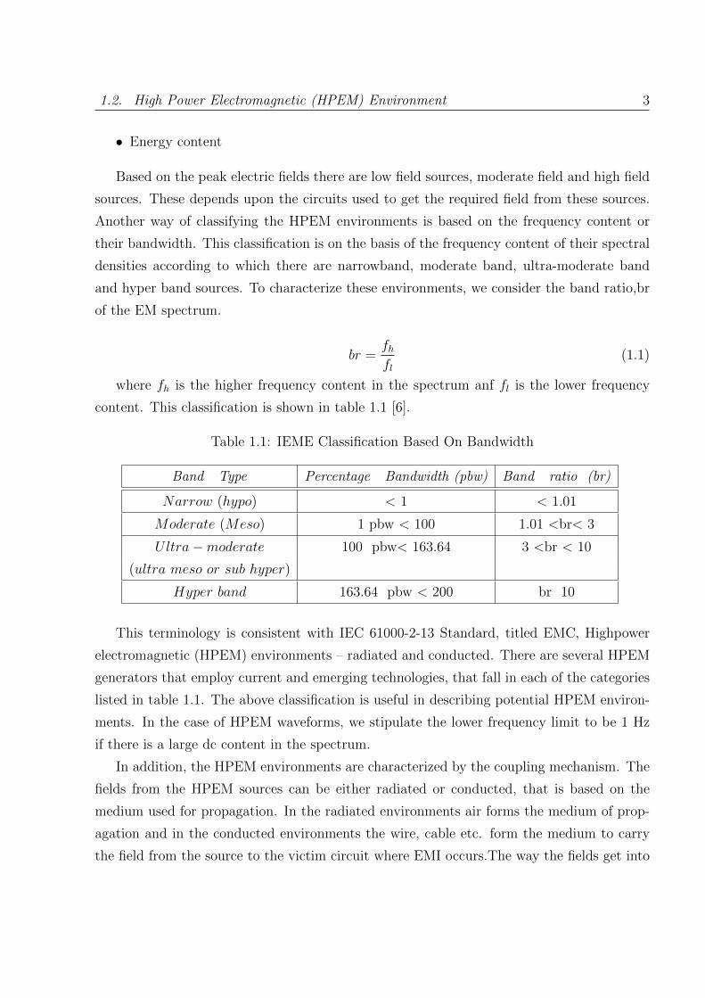
1.2. High Power Electromagnetic (HPEM) Environment 3
• Energy content
Based on the peak electric fields there are low field sources, moderate field and high field
sources. These depends upon the circuits used to get the required field from these sources.
Another way of classifying the HPEM environments is based on the frequency content or
their bandwidth. This classification is on the basis of the frequency content of their spectral
densities according to which there are narrowband, moderate band, ultra-moderate band
and hyper band sources. To characterize these environments, we consider the band ratio,br
of the EM spectrum.
br =fhfl
(1.1)
where fh is the higher frequency content in the spectrum anf fl is the lower frequency
content. This classification is shown in table 1.1 [6].
Table 1.1: IEME Classification Based On Bandwidth
Band Type Percentage Bandwidth (pbw) Band ratio (br)
Narrow (hypo) < 1 < 1.01
Moderate (Meso) 1 pbw < 100 1.01 <br< 3
Ultra−moderate 100 pbw< 163.64 3 <br < 10
(ultra meso or sub hyper)
Hyper band 163.64 pbw < 200 br 10
This terminology is consistent with IEC 61000-2-13 Standard, titled EMC, Highpower
electromagnetic (HPEM) environments – radiated and conducted. There are several HPEM
generators that employ current and emerging technologies, that fall in each of the categories
listed in table 1.1. The above classification is useful in describing potential HPEM environ-
ments. In the case of HPEM waveforms, we stipulate the lower frequency limit to be 1 Hz
if there is a large dc content in the spectrum.
In addition, the HPEM environments are characterized by the coupling mechanism. The
fields from the HPEM sources can be either radiated or conducted, that is based on the
medium used for propagation. In the radiated environments air forms the medium of prop-
agation and in the conducted environments the wire, cable etc. form the medium to carry
the field from the source to the victim circuit where EMI occurs.The way the fields get into

4 Chapter 1. Introduction
Figure 1.1: Different Modes of Coupling
the victim circuits can be either as a front-door coupling or by back-door as shown in Fig.
1.1. In the front door coupling, the fields get into the system or the equipments by way of
the antennas, sensors etc. that are installed in the system. In the back door coupling this
field penetration occurs through holes and other cavities or slots available in any part of the
circuit.
All these characterizations are intended to provide information needed to estimate the
effects caused by HPEM environments. If one is assessing the risk that an HPEM environ-
ment causes hazardous situations in a given system one will have to focus more on aspects
like
• Likelihood of occurrence of the HPEM environment under real life conditions (i.e.
outside a laboratory)
• Ability to access the target system (i.e. come close to the target (radiated) or connect
to a cable (conducted)
• Sensitivity of the target to the specific HPEM environment
The HPEM environment is shown in Fig 1.2. It includes lightning, High altitude Elec-
tromagnetic Pulse (HEMP) due to nuclear detonations, Ultra Wide Band (UWB) field from
Impulse Radiating Antennas (IRA), Narrow band fields like those coming from HPM, HIRF
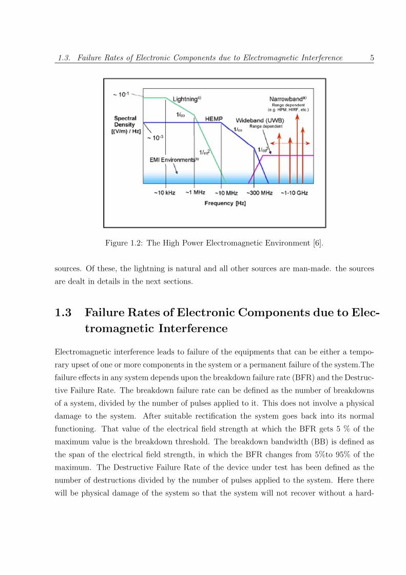
1.3. Failure Rates of Electronic Components due to Electromagnetic Interference 5
Figure 1.2: The High Power Electromagnetic Environment [6].
sources. Of these, the lightning is natural and all other sources are man-made. the sources
are dealt in details in the next sections.
1.3 Failure Rates of Electronic Components due to Elec-
tromagnetic Interference
Electromagnetic interference leads to failure of the equipments that can be either a tempo-
rary upset of one or more components in the system or a permanent failure of the system.The
failure effects in any system depends upon the breakdown failure rate (BFR) and the Destruc-
tive Failure Rate. The breakdown failure rate can be defined as the number of breakdowns
of a system, divided by the number of pulses applied to it. This does not involve a physical
damage to the system. After suitable rectification the system goes back into its normal
functioning. That value of the electrical field strength at which the BFR gets 5 % of the
maximum value is the breakdown threshold. The breakdown bandwidth (BB) is defined as
the span of the electrical field strength, in which the BFR changes from 5%to 95% of the
maximum. The Destructive Failure Rate of the device under test has been defined as the
number of destructions divided by the number of pulses applied to the system. Here there
will be physical damage of the system so that the system will not recover without a hard-

6 Chapter 1. Introduction
Table 1.2: Susceptibility Levels of Equipments for Destruction Failure [6]
EUT UWB in kV/m EMP in kV/m HPM in kV/m
Logic Devices 25 120 NA∗
Microcontroller 7.5 42 NA
Microprocessor Boards 4 25 0.2
PC Systems 12 NA NA
PC Networks 0.2 0.5 NA
∗ data not available.
ware repair [14]. The susceptibility levels of different equipments under an interference due
to high power sources like Ultra Wide Band Pulse (UWB), Electromagnetic Pulse (EMP)
and High Power Microwave (HPM) are shown in table 1.2.
The destruction of the devices occurs depending upon the field strengths. At lower field
strengths electronic components such as diodes or transistors on the chip will be damaged
that are mainly due to flash over effects. If the amplitude of the electromagnetic pulse
increases by about 50%, additional on chip wire destructions like smelting of PCB tracks
without flash over effects and multiple component destructions can occur. Further increase
in the amplitude leads to additional bond wire destructions, multiple components, and on
chip wire destructions. On that account it is possible to predict the destruction effects of
integrated circuits on chip level, if the proposed measurement set-up is used [15]-[21].
1.4 Nuclear Electromagnetic Pulse (NEMP)
A high altitude nuclear burst produces Nuclear Electro Magnetic Pulses (EMP) in addition
to the generation of heat, light and nuclear radiation. These electromagnetic pulses are pro-
duced at the same time as the blast itself and can illuminate a large geographical area. The
electromagnetic fields produced by the EMP can induce large voltage and current transients
in electrical and electronic circuits which can lead to a possible malfunction or permanent
damage of the systems [22]-[30] . The typical electromagnetic pulse waveform at the earth’s
surface is given in Fig. 1.3. The probability of damage of the electronic devices is higher
if their sensitivity is more. This makes it important that the electronic devices and circuits
be hardened so as to reduce the damage level due to EMP. Consequently, there is a great

1.4. Nuclear Electromagnetic Pulse (NEMP) 7
Figure 1.3: The Typical Electromagnetic Pulse.
need for laboratory simulation and measurement of EMP. The origin, classification, physics
of generation and characteristics of EMP will be presented in this chapter [22]-[30].
1.4.1 Origin of EMP
Nuclear bombs when detonated can produce electromagnetic signals and this leads to the
generation of EMP. However, the extent and potentially dangerous nature of EMP effect
were not realized for several years. Only during the atmospheric nuclear tests in the early
1950s that attention slowly began to focus on EMP as a probable cause of malfunction of
electronic equipments. Finally, around 1960, the possible vulnerability of various civilian
and military electrical and electronic systems to EMP was recognized. Although and EMP
may be caused by non-nuclear explosions as well, the present usage of the term EMP is such
that it refers to EMP of nuclear origin exclusively [31]-[36].
Nuclear explosions of all types from underground to high altitudes are accompanied
by an EMP, although the intensity and duration of the pulse and the area over which it
is effective vary considerably with the location of the burst point with respect to earth’s
surface. The strongest electric fields are produced near the burst by explosions at or near
8 Chapter 1. Introduction
the earth’s surface, but for those at high altitudes the fields at the earth’s surface are strong
enough to be of concern for electrical and electronic equipments over a very much larger area
[31]-[36].
Majority of the EMP energy lies within the radio frequency spectrum ranging from a few
hertz to the very high frequency (VHF) band. The pulse is characterized by electromagnetic
fields with short rise times and a high peak electric field amplitude (tens of kilovolts per
meter) [31]-[36]. A significant property of EMP is its large area of coverage; intense fields from
a single burst outside the atmosphere can cover an area of earths surface several thousand
kilometres in diameter. EMP thus differs from many other sources of electromagnetic energy,
whether natural (lightning) or man-made (such as HPM and ESD). EMPs time waveform
exhibits a higher amplitude and shorter rise time. Also, the electromagnetic radiation due
to EMP can occur almost at the same time (the limitation being the speed of light) over a
large area. Intense natural and man-made fields, on the other hand, seldom have such wide
simultaneous distribution. Also, while natural and man-made sources are usually confined
to a narrow portion of the frequency spectrum, EMP occupies a broad frequency spectrum
from a few hertz to the VHF band (> 100 MHz).
1.4.2 Classification of EMP Environment
EMPs major characteristics its time signature and spatial extent depend primarily on
the height and location of the nuclear burst relative to the point of observation [31]-[36].
EMP is thus often classified according to burst height, namely surface, air or high altitude.
A surface burst occurs on or close to the ground, and an air burst takes place between 2
and 20 kilometres above the ground. Bursts occurring above 40 kilometres are classified
as high altitude bursts. However, a burst between 0 and 2 kilometres produces an EMP
with characteristics of both surface and air bursts and those between 20 and 40 kilometres
generate EMP with characteristics of both air and high-altitude bursts.
Two regions surrounding the nuclear burst are important in EMP considerations namely
the deposition (source) region and the radiation region. The deposition region is the space
around the burst where the EMP is generated. It contains intense electric and magnetic
fields as well as a highly conducting plasma (ionized gas). The deposition region is limited
to a radius of 3 to 6 kilometers around a surface burst, about 5 to 15 kilometers around an
air burst and about 3000 kilometers for a high-altitude burst.

1.4. Nuclear Electromagnetic Pulse (NEMP) 9
Depending upon the burst height, the geomagnetic field and/or asymmetries in the envi-
ronment cause the source fields to radiate well beyond the deposition region. These radiation
regions contains somewhat less intense fields and have three general characteristics, viz.,
(1) the direction of propagation is radially outward from the burst,
(2) the electric and magnetic field vectors are in a plane perpendicular to the direction
of propagation,
(3) the fields have a far-field range dependence of 1/R.
Although all three types of bursts produce a radiated pulse, they differ in time waveform
and spatial coverage. High-altitude EMP can have a strong radiated electromagnetic field
and a wide area of coverage. An air burst produces a relatively weak radiated field but
can have a large non-radiated field. Surface burst EMP is characterized by a large non-
radiated field and a significant radiated field. In the present work, a High Altitude EMP
is considered. The physics of generation of High Altitude EMP, the various models for
explaining the generation of EMP are reported in many literatures [31]-[42].
1.4.3 Characteristics of High Altitude EMP
A high altitude nuclear burst differs from the surface and air bursts in that EMP is the
major effect. There is no significant overpressure pulse and the atmosphere diminishes all
other prompt weapon effects.
The radiated fields due to high altitude EMP have very intensity; short rise times and
they cover a wide area because of the height and large extent of the source region.
The characteristics such as the spatial extent, time waveform and peak amplitude of
high altitude EMP depend on the height of burst (HOB), weapon yield, and the observer’s
location in relation to the burst [31]-[42].
1.4.3.1 Spatial Extent
The geographical coverage of high altitude EMP over the earth’s surface is determined en-
tirely by the height of burst.
As shown in Fig. 1.4, the maximum ground range (tangent radius) depends on the
tangent to the earth from the burst point and is the arc length between this tangent and the
earth’s surface directly beneath the burst (surface zero).
Assuming that the earth is spherical, the tangent radius RT (in kilometres) is
10 Chapter 1. Introduction
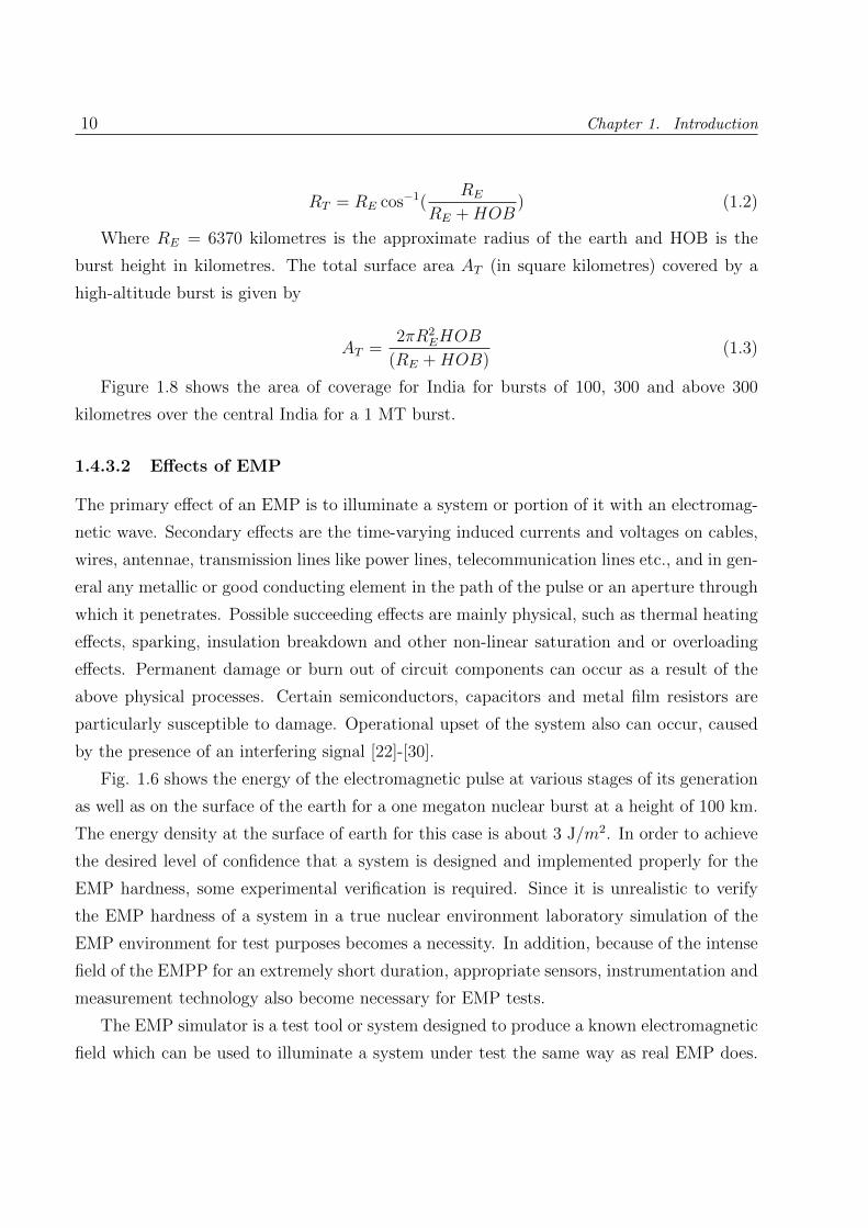
RT = RE cos−1(RE
RE +HOB) (1.2)
Where RE = 6370 kilometres is the approximate radius of the earth and HOB is the
burst height in kilometres. The total surface area AT (in square kilometres) covered by a
high-altitude burst is given by
AT =2πR2
EHOB
(RE +HOB)(1.3)
Figure 1.8 shows the area of coverage for India for bursts of 100, 300 and above 300
kilometres over the central India for a 1 MT burst.
1.4.3.2 Effects of EMP
The primary effect of an EMP is to illuminate a system or portion of it with an electromag-
netic wave. Secondary effects are the time-varying induced currents and voltages on cables,
wires, antennae, transmission lines like power lines, telecommunication lines etc., and in gen-
eral any metallic or good conducting element in the path of the pulse or an aperture through
which it penetrates. Possible succeeding effects are mainly physical, such as thermal heating
effects, sparking, insulation breakdown and other non-linear saturation and or overloading
effects. Permanent damage or burn out of circuit components can occur as a result of the
above physical processes. Certain semiconductors, capacitors and metal film resistors are
particularly susceptible to damage. Operational upset of the system also can occur, caused
by the presence of an interfering signal [22]-[30].
Fig. 1.6 shows the energy of the electromagnetic pulse at various stages of its generation
as well as on the surface of the earth for a one megaton nuclear burst at a height of 100 km.
The energy density at the surface of earth for this case is about 3 J/m2. In order to achieve
the desired level of confidence that a system is designed and implemented properly for the
EMP hardness, some experimental verification is required. Since it is unrealistic to verify
the EMP hardness of a system in a true nuclear environment laboratory simulation of the
EMP environment for test purposes becomes a necessity. In addition, because of the intense
field of the EMPP for an extremely short duration, appropriate sensors, instrumentation and
measurement technology also become necessary for EMP tests.
The EMP simulator is a test tool or system designed to produce a known electromagnetic
field which can be used to illuminate a system under test the same way as real EMP does.

1.4. Nuclear Electromagnetic Pulse (NEMP) 11
Figure 1.4: EMP Ground Coverage
Figure 1.5: EMP Ground Coverage for High Altitude Bursts at 100 and 200 km.
Figure 1.6: EMP Energy from the High Altitude Burst [36].
12 Chapter 1. Introduction
Therefore an idealized EMP facility should produce a wave shape, similar to the double
exponential waveform shown. It should also have some over test capability (in higher magni-
tudes of E and H fields). The facility should have the capability of orienting the test object
to account for polarization and direction of arrival. Also, an ideal EMP simulator should
produce plane waves with a ratio of E/H equal to 120π. In addition, the fields produced by
such a facility should not be unduly affected by the test object. In practice, however, there
is no facility which achieves all the desirable characteristics.
1.5 Impulse Radiating Antenna (IRA)
Impulse radiating antennas are powerful and highly efficient antennas which are used as a
major source of Ultra Wide Band (UWB) radiation. These antennas uses a pulsed power
source as input and this power source is conditioned to get an extremely sharp rise time
pulse [43]-[44]. These antennas are capable of producing an intense electromagnetic field.
Impulse radiating antennas are driven by high voltages with very sharp rise times. these
high voltages generate the field that gets reflected from the antenna used in the IRA so that
the net electric field at the required observation point has the characteristics of a sharp rise
time, impulse nature and very high peak electric field.Typically the rise time is of the order
of pico-seconds and the voltage rating will be in kilovolts and the electric field will be of
the order of kV/m. there are very powerful IRA’s like JOLT that operate with a million
volts input voltage at pico-second rise time which gives electric fields of about 100’s of kV/m
magnitude. The major components of an Impulse Radiating Antenna (IRA) are as shown
in the block diagram of Fig. 1.7 and includes a primary energy storage, a pulse generator,a
pulse sharpening system and an antenna.
IRA has a number of applications including underground object detection, periscope
detection, to determine the characteristics of rocks, for atmospheric studies and so on.
1.5.1 Primary Energy Storage
the energy required for driving the entire power circuit of the IRA comes from the primary
energy storage. this consists of either a capacitor or an inductor that can store energy in its
electric/magnetic field respectively. If inductors are used as energy storage there are chances
of more losses occurring by way of leakage. This seriously affects the performance of the
1.5. Impulse Radiating Antenna (IRA) 13
circuit. Hence it is not possible to get the required high voltage and the sharp rise time.
Since the major characteristics of IRA includes its sharp rise time and high peak electric
field,inductors are not a good choice for energy storage.
The primary energy storage commonly used are capacitors that store energy in its electric
field. Such an energy storage device is shown in Fig. 1.8. The energy stored in these
capacitors are given to the load which is the antenna through a series of circuit components.
There can be losses occurring in this process of energy transportation of this energy. Hence
if a single capacitor is used it may not be able to handle the total energy that is to be needed
by the circuit. Hence in all commercial IRA’s, instead of using a single capacitor, a number
of capacitors are stacked together so that the net energy storage is increased. The number
of capacitors stacked are a function of the magnitude of the output voltage required [44].
In the case of stacked capacitors, there should be proper insulation of the entire unit
else it can lead to a failure at the pulsed voltage levels. A co-axial geometry is usually
chosen so as to get a minimum inductance. The capacitors are mainly ceramic capacitors
mounted between the inner and outer aluminium conductors.these capacitor assembly is kept
in dielectric boxes that are made out of thick acrylic. Suitable elastomers are added to give
the dielectric protection. One such elastomer is silicone which is used in the most powerful
IRA known as JOLT [46].
1.5.2 Pulse Generator
The major part of an IRA is the pulse generator. This receives the enrgy from the primary
energy storage and it has a number of circuits including the capacitors, inductors transform-
ers and spark gaps that finally helps in building the voltage levels to the required magnitude
that is to be used by the antenna. To generate high voltage pulses with voltage amplitudes
of several 100 kV ′s there are two major technologies known, Marx Generators, and Tesla
Transformer.
1.5.2.1 Marx Generator [46]
A Marx generator is an efficient impulse generator, where charging and discharging of ca-
pacitors are used to get the required impulse voltage. the capacitors are charged in parallel
and discharged in series. Usually these impulse generating circuits are meant for generating
impulses with a rise time of the order of µs. But in an IRA the voltage must be either in

14 Chapter 1. Introduction
Figure 1.7: The Block Diagram Showing the Different Components of an IRA [44].
Figure 1.8: Capacitive Energy Storage [46].
Figure 1.9: A Capacitor Assembly [46].

1.5. Impulse Radiating Antenna (IRA) 15
tens or hundreds of kV or even more with rise time of the order of pico- seconds. Hence the
Marx generator circuit uses capacitors rated in nano farads or even in pico farads. The stray
inductance of the circuit should be as minimum as possible. The major draw back of using
Marx generator in IRA application involves the number of switches required to produce the
required output waveform. So operation of large number of switches in this case can cause
jitter in the performance which can seriously damper the efficiency of the IRA. So this jitter
must be avoided. There are several methods used to avoid jitter in the operation. They are:
• A compact, lightweight, and portable design of Marx generator that is housed in a
tubular containment pressure vessel.In this case the Marx generator works in an atmo-
sphere of pressurized dry air. this improves the pulse repetation rates of the IRA.
• A configurable output polarity using a single polarity charging source
• A modular construction that allows setting the output voltage and pulse width as
desired
• Utilization of corona-stabilized (or field enhanced) spark gap switches for high PRR
operation
• Optical coupling of spark gap switches to reduce system jitter
• A triggering scheme that allows for a subnanosecond command trigger to output jitter
• Parallel resonant charging using a series inductance and resistance in each stage to
support high pulse repetation rate operation
Low jitter triggering of the Marx generator requires a bipolar trigger input. The con-
ventional Marx generator used a trigatron switch in the first stage and only the first stage
switch was triggered. In the case of a bipolar trigger input,a dual pulsed trigatron switch
is used to improve the performance. Fig. 1.11 shows schematically the new dual-pulsed
trigatron switch configuration as it would be employed in the first two stages of a Marx
generator. The circuit in Fig. 1.11 is quite similar to a standard trigatron circuit. However,
the positive going output of trigger transformer T1 is coupled through trigger capacitor Ct
to the anode of the first stage switch. When the trigger pulse is first applied, almost the full
potential drop occurs across the trigger gap T-K which rapidly breaks down. This is because
16 Chapter 1. Introduction
the capacity of the trigger gap is much smaller than the series combination of capacitors Ct
and Cp. When the trigger gap closes, the full transformer potential is rapidly applied to the
switch anode and heater capacitor Cp. This circuit achieves a simultaneous UV illumination
of gas molecules in the gap and over-voltage of the gap potential. The heater capacitor Cp
rapidly heats the discharge channel and switch closure causes the large potential to appear
on the cathode of the following stage [45].
Because of the lower efficiency of the Marx generator , Tesla transformers are used as a
better option for pulse generation [43]-[48].
1.5.2.2 Tesla Transformer
Tesla transformers are air cored transformers that are highly efficient in the transfer of energy
from its primary side to the secondary high voltage side. They operate based on the principle
of resonance in either primary or the secondary side. The Tesla Transformer technology is
widely used in IRA because of the following reasons:
• Compact size
• Low input voltage on primary side
• Low energy requirements of the pulser
• Capability to run easier on higher repetition rates
• Only one single switch
The low pulse energy requirements for the generation of UWB pulses with rise times
<500 ps and pulse width < 1 ns gave the Tesla Transformer an advantage against the Marx
Generator. Fig. 1.12 shows the Tesla Transformer. For sharp rise times needed for the
input voltage to IRA, the tesla transformer operates in the pressurized gas atmosphere so
that the switchings and the transfer of energy is more efficient. For optimum performance of
the Tesla Transformer the resonance frequency of the primary side and the secondary side
should be very close, therefore all stray capacitance and inductivities must be considered
while designing the system [45].

1.5. Impulse Radiating Antenna (IRA) 17
Figure 1.10: Marx Generator [46].
Figure 1.11: Dual Trigatron Switch of a Low Jitter type Pulse Generator [45].
Figure 1.12: Tesla Transformer [45].

18 Chapter 1. Introduction
1.5.3 Pulse Sharpening System
The pulse sharpening system is used when a transient pulse of fast rise time is required
[43]-[44]. Pulse sharpening system mainly uses a spark gap and the switching speed of the
spark gap decides the rise time attained by the pulse at the output of the pulse sharpening
circuit.
A pulse sharpening system of three sections, charge line, pulse line, and load line as
shown in Fig. 1.13. Each line is separated from the other by a discharge gap. The charge
line is connected to the output of the pulse generator circuit. It actually decides the charging
rate of the spark gaps and also decides a higher switching rate or a normal switching rate is
required based on the rise time required. Pulse line actually produces the pulse which has
the required rise time and is fed to the load line where fine tuning of the rise time and the
field occurs so that at the output of the load line the pulse has the required magnitude and
rise time for the electric field. The characteristic impedances of all the three sections must
be properly designed to get the required output characteristics.
Spark gaps being the important component in a pulse sharpening system, the size, the
gap distance and the type of the spark gaps plays an important role in its efficient operation.
As rise time of the odder os pico-seconds are necessary for IRA , the spark gaps are needed to
operate in an atmosphere where the switching can be done faster. Usually highly pressurized
hydrogen gas is used so that the required rise times can be obtained.The generation of pulse
rise times less than 500 ps at pulse amplitudes above 100 kV is normally done by fast over
charging a spark gap. The gap will then see a higher voltage as the switching is done faster
than at a low charging rate, this causes a higher electrical field strength between the gaps.
By placing several gaps in series, the leading edge of the pulse could be sharpened.
Figure 1.13: Pulse Sharpening System [43].
1.5. Impulse Radiating Antenna (IRA) 19
1.5.4 Antennas
UWB systems need special antennas for receiving or transmitting short pluses with risetimes
less than 1 ns. Ordinary wideband antennas are generally not able to transmit short pulses,
because of the dispersion. There are several antenna designs for transmitting ultra short
pulses [43]-[70]. The typical antennas are:
• Paraboloidal Antenna
• TEM horn antenna
• Half IRA
• Collapsible IRA
1.5.4.1 Paraboloidal Antenna
A parabolic reflector (or dish or mirror) is a reflective device used to collect or project energy
such as light, sound, or radio waves. It has a circular paraboloid shape. The parabolic
reflector transforms an incoming plane wave travelling along the axis into a spherical wave
converging toward the focus. Conversely, a spherical wave generated by a point source placed
in the focus is transformed into a plane wave propagating as a collimated beam along the axis.
In IRA it is the second principle that is used. This is the most directive type of antenna.
A parabolic antenna is a high-gain reflector antenna used for radio, television and data
communications, and also for radio location (radar), satellite television, extensive terrestrial
microwave links, such as those between cellphone base stations, and wireless WAN/LAN
applications have also proliferated this antenna type,ground-based and airborne radar and
radio astronomy.A parabolic reflector antenna is shown in Fig. 1.14a.
1.5.4.2 Horn Antenna
A horn antenna is essentially an open-ended wave guide, of increasing cross-sectional area,
which radiates directly in a desired direction or feeds a reflector that forms a desired beam.
Horn antenna has an E-plane and an H-plane where the field is either electric or magnetic
respectively. A very wide range of beam patterns may be formed by controlling horn dimen-
sions and shapes, placement of the reflector, and reflector shape and dimensions. A horn
antenna is shown in Fig. 1.14b.

20 Chapter 1. Introduction
1.5.4.3 Half IRA
The major task of the antenna design is to minimise the frequency and spatial dispersion,
and to increase the capability of operating voltage. For compact UWB source a half IRA
design has same advantages when connecting the source to the antenna. The basic idea
behind the half IRA is to operate only with one half of the antenna and to use the electrical
symmetry plane at ground potential as a mirror for the electrical field below the antenna
. The cylindrical electrical field distribution of the pulse line is converted by the two feed
arms into a plane electrical field which is transmitted by the mirror. A compact gas switched
UWB source and the half IRA is shown in Fig. 1.14c.
1.5.4.4 Collapsible IRA
It is a wideband antenna that could be used by ground troops and is of lightweight and
portable. This IRA shown in Fig. 1.14d., that is made of conducting fabric. This antenna
can fold up like an umbrella. It can perform efficiently from high frequency to X-band [64].
1.5.5 Switches
Switches are a necessary part of the IRA system.The switches are designed so that they are
compact,lower probabilities of bulk and surface breakdown. the material used for making
switches should have the necessary properties such as durability, high mechanical end elec-
trical strength to withstand a breakdown and so on. There are lot of materials with desirable
electrical and mechanical properties that are capable of making switches. The different types
of switches used are [43]-[58]:
• High pressure hydrogen switch
• Triggered gas switches
• Oil Switches
• Solid-State Switching
High Pressure hydrogen switches are the most commonly used category of switches for
IRA’s. This is because they are capable of withstanding voltages upto 1 MV at repetation
rates of 100s of Hz. The switch is composed of copper tungsten electrodes with a coaxial

1.5. Impulse Radiating Antenna (IRA) 21
(a) (b)
(c) (d)
Figure 1.14: Different Antennas (a) Paraboloidal antenna (b) Horn antenna (c) Half reflector
IRA (d) Collapsible IRA [43]-[70].
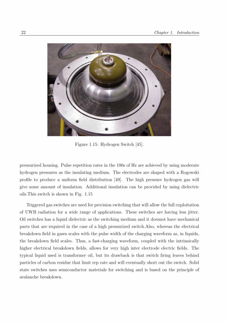
22 Chapter 1. Introduction
Figure 1.15: Hydrogen Switch [45].
pressurized housing. Pulse repetition rates in the 100s of Hz are achieved by using moderate
hydrogen pressures as the insulating medium. The electrodes are shaped with a Rogowski
profile to produce a uniform field distribution [49]. The high pressure hydrogen gas will
give some amount of insulation. Additional insulation can be provided by using dielectric
oils.This switch is shown in Fig. 1.15
Triggered gas switches are used for precision switching that will allow the full exploitation
of UWB radiation for a wide range of applications. These switches are having less jitter.
Oil switches has a liquid dielectric as the switching medium and it doesnot have mechanical
parts that are required in the case of a high pressurized switch.Also, whereas the electrical
breakdown field in gases scales with the pulse width of the charging waveform as, in liquids,
the breakdown field scales. Thus, a fast-charging waveform, coupled with the intrinsically
higher electrical breakdown fields, allows for very high inter electrode electric fields. The
typical liquid used is transformer oil, but its drawback is that switch firing leaves behind
particles of carbon residue that limit rep rate and will eventually short out the switch. Solid
state switches uses semiconductor materials for switching and is based on the principle of
avalanche breakdown.
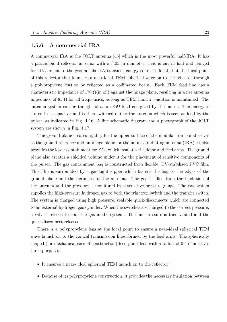
1.5. Impulse Radiating Antenna (IRA) 23
1.5.6 A commercial IRA
A commercial IRA is the JOLT antenna [45] which is the most powerful half-IRA. It has
a paraboloidal reflector antenna with a 3.05 m diameter, that is cut in half and flanged
for attachment to the ground plane.A transient energy source is located at the focal point
of this reflector that launches a near-ideal TEM spherical wave on to the reflector through
a polypropylene lens to be reflected as a collimated beam. Each TEM feed line has a
characteristic impedance of 170 Ω(in oil) against the image plane, resulting in a net antenna
impedance of 85 Ω for all frequencies, as long as TEM launch condition is maintained. The
antenna system can be thought of as an 85Ω load energized by the pulser. The energy is
stored in a capacitor and is then switched out to the antenna which is seen as load by the
pulser, as indicated in Fig. 1.16. A line schematic diagram and a photograph of the JOLT
system are shown in Fig. 1.17.
The ground plane creates rigidity for the upper surface of the modular frame and serves
as the ground reference and an image plane for the impulse radiating antenna (IRA). It also
provides the lower containment for SF6, which insulates the dome and feed arms. The ground
plane also creates a shielded volume under it for the placement of sensitive components of
the pulser. The gas containment bag is constructed from flexible, UV-stabilized PVC film.
This film is surrounded by a gas tight zipper which fastens the bag to the edges of the
ground plane and the perimeter of the antenna. The gas is filled from the back side of
the antenna and the pressure is monitored by a sensitive pressure gauge. The gas system
supplies the high-pressure hydrogen gas to both the trigatron switch and the transfer switch.
The system is charged using high pressure, sealable quick-disconnects which are connected
to an external hydrogen gas cylinder. When the switches are charged to the correct pressure,
a valve is closed to trap the gas in the system. The line pressure is then vented and the
quick-disconnect released.
There is a polypropylene lens at the focal point to ensure a near-ideal spherical TEM
wave launch on to the conical transmission lines formed by the feed arms. The spherically
shaped (for mechanical ease of construction) feed-point lens with a radius of 0.457 m serves
three purposes.
• It ensures a near- ideal spherical TEM launch on to the reflector
• Because of its polypropylene construction, it provides the necessary insulation between

24 Chapter 1. Introduction
Figure 1.16: Different Forms of the Equivalent Circuit for the JOLT Hyperband System [45].
Figure 1.17: Photograph of the JOLT Hyperband System [45].

1.6. High Power Microwaves (HPM) 25
the feed arms and the ground plane
• It provides an inner containment dome for the high-velocity transformer oil, which is
used to clear debris from the peaker switch
The electric fields inside the lens are held-off by the oil insulating medium. However,
outside the spherical lens medium, SF6 gas is present at 1 atmosphere pressure and the
electric field has hot spots or field maxima around the feed arm conductor protruding out
of the lens. The interface between the lens and the outside gas medium could have two
dielectric discontinuities (oil/container and container/gas).
All these circuits except the primary energy source are kept in a polypropylene container
called pulser,since this container has the same dielectric constant as that of the dielectric oil.
The closing of the high pressure hydrogen gas switch in the pulser generates a TEM wave
that gets out of the pulser towards the reflector, where it gets reflected and hence is available
at the observation point. The electric field at any observation point has a prepulse and an
impulse that are characteristic features of the distance of the observation point from the
antenna and also on the characteristics of the voltage in the pulser.
1.6 High Power Microwaves (HPM)
HPM sources are usually electromagnetic radiators having a reflector with a horn antenna
kept at their focal point for excitation. HPM sources generally operate in single mode or at
tens or hundreds of Hz repetition rates. Many HPM radiators are developed in the world each
with their own peculiar geometry and power levels. The frequencies ranging between 300
MHz to 300 GHz are usually named as the microwave frequencies, whose wavelengths vary
from 1 m to 1 mm. A microwave transmission consists of a microwave source, a wave guide,
a transmitting antenna, a propagation path, a receiving antenna, another wave guide and
finally a receiver. Microwave generation can be accomplished in different ways depending
upon the different varieties of the sources used such as klystrons, magnetrons, gyratrons
etc. Basically, the kinetic energy of the charged particle which is electrons in a beam is
converted into microwave energy in all these sources. Hence wave particle interaction is the
fundamental principle which results in the generation of high power microwaves [71]-[77].
HPM sources are transient generators that produces a short burst of energy, lasting for
about a microsecond or less. The basic block diagram for an HPM generator is shown in

26 Chapter 1. Introduction
Fig. 1.18.
HPM radiating systems consists of an HPM source with a single rectangular wave guide
feeding an evacuated feed horn through a series of vacuum flanges as shown in Fig. 1.19.
The output of this system is connected to an offset Cassegrain system as shown in Fig.
1.20. This gives a directed HPM radiation. The radiation coming out of the antenna can
cause severe electromagnetic interference. The power to this antenna assembly is fed from
evacuated rectangular wave guides, the number of wave guides depending upon the power
level required. In the present study a single WR-975 wave guide fed HPM antenna assembly
has been considered. This has a dominant H1,0 mode at the cut-off frequency of 1 GHz and
power level of 10 GW. The peak electric field of the wave guide is 25 MV/m. The wavelength
associated with the wave guide is 0.3 m.
1.6.1 Applications of HPM
• Particle accelerators
• Wireless power transmission
• Controlled fusion reaction
• Plasma heating for magnetic confinement fusion
• High power and high resolution radars
• Military defense applications to disrupt or destroy offensive electronic systems like high
power jammers
1.7 Objectives of the thesis
Study of different Intentional HPEM sources:
The different HPEM sources considered are NEMP, IRA and HPM. The characteristics
of these sources are to be studied and the way the electromagnetic field is generated from
these sources are analysed.
Computation of electromagnetic field due to HPEM sources: The electromag-
netic fields due to the HPEM sources is to be determined at a given distance from the source
in the case of IRA and HPM sources and at earths surface in the case of NEMP source.

1.7. Objectives of the thesis 27
Figure 1.18: The Basic Block Diagram for an HPM Generator.
Figure 1.19: Elements of a Single Waveguide feed system [71].
Figure 1.20: A Single Reflector fed by a Feed Horn [71].

28 Chapter 1. Introduction
Effect of the ambient media on the propagation of the electromagnetic field:
The effect of the properties of the media such as air and the soil affects the propagation
characteristics of the electromagnetic field. This knowledge is essential before proceeding to
study the coupling of the field with a buried cable and an airborne vehicle.
Coupling of the electromagnetic fields due to HPEM sources with a buried
cable:
Computation of the induced current and voltage in a buried shielded and twisted pair
cables due to the incoming electromagnetic field due to HPEM sources. This involves the
analysis of the cable parameters, the method of coupling adopted and finally computation
of the induced current and voltage.
Coupling of the electromagnetic fields due to HPEM sources with an airborne
vehicle in flight:
Electromagnetic modelling of the plume of an airborne vehicle, and computation of the
induced current and voltage in the vehicle in the presence and absence of the plume to
determine the effect of the plume on the coupling phenomenon.
1.8 Organization of the thesis
The thesis is organized as follows:
Chapter 1: Introduction:
The effect of the HPEM sources on the different systems are presented.The different
HPEM sources considered are NEMP, IRA and HPM. The characteristics of these sources
are presented and the way the electromagnetic field is generated from these sources are
discussed.
Chapter 2: Electric field due to HPEM Sources:
The electromagnetic fields due to the HPEM sources is determined at a given distance
from the source in the case of IRA and HPM sources and at earths surface in the case of
NEMP source.
Chapter 3: Effect of the ambient media on the electric field from IEMI
sources:
Two types of media are considered in this chapter- air and the soil. The characteristic
properties of both these media are considered. The effect of the properties of the media such
as air and the soil affects the propagation characteristics of the electromagnetic field. This

1.8. Organization of the thesis 29
knowledge is essential before proceeding to the coupling of the field with a buried cable and
an airborne vehicle.
Chapter 4: Coupling on a buried cable:
The cable is considered to be buried in the soil. Computation of the induced current and
voltage in a buried shielded and twisted pair cables due to the incoming electromagnetic
field due to HPEM sources. This involves the analysis of the cable parameters, the method
of coupling adopted and finally computation of the induced current and voltage.
Chapter 5: Coupling of the field due to IEMI with an airborne vehicle in
flight:
Electromagnetic modelling of the plume of an airborne vehicle, and computation of the
induced current and voltage in the vehicle in the presence and absence of the plume to
determine the effect of the plume on the coupling phenomenon has been presented in this
thesis .
Chapter 6: Conclusion: The conclusion and the scope for future work are presented
in this chapter, along with a summary of the chapters 2 to chapter 5.

Chapter 2
Electric Field due to Intentional
HPEM Sources
2.1 Electric Field from a Nuclear Burst
The radiated fields due to a high altitude EMP incident on the earths surface could be
modelled locally by a plane electromagnetic wave, where the ratio of the magnitude of the
electric field strength E (V/m) to the magnitude of the magnetic field strength H (A/m) is
the impedance of free space [36].
E
H= 377 Ω (2.1)
Since the motion of the Compton electrons depends on the orientation of geomagnetic
field, the incident EMP fields vary significantly (in peak amplitude, rise time and duration)
over the large area affected by the EMP. The maximum peak electric field Emax occurs just
south of surface zero and can be as high as 50 kV/m depending upon the height of burst and
the weapon yield. The peak field observed at any other location is some fraction of Emax.
The variations in peak electric fields on the earths surface for high-altitude bursts ranging
in height from 100 to 500 km is shown in Fig. 2.1.
In addition to the orientation and dip of the geomagnetic field, geometric factors based
on the observer’s position in relation to the burst also cause spatial variations of the EMP
field strength. The maximum peak fields are found at 2 x HOB south of surface zero. The
EMP time waveform also varies considerably over the area of coverage. Near surface zero,
the EMP has a rise time of about 5 ns (10 to 90% of the peak field) and a time to half value
of 20 ns. In the region of maximum peak fields, the rise time is just under 10 ns with a time
30

2.1. Electric Field from a Nuclear Burst 31
to half-value of about 50 ns. Finally, near the tangent radius due south of the burst, the rise
time is somewhat longer than 10 ns and the time to half-value is about 200 ns.
2.1.1 Polarization and Ground Effects
The polarization of the EMP is also a significant factor in its coupling to communication
facility and to the external structures that service it like power lines, communication cables,
microwave towers etc. The polarization depends on the locations of both the burst and the
observer and on the orientation of the geomagnetic field.
The EMP fields described up to now are only incident fields. The total fields at any point,
however also include the reflection of these fields from the ground plane. The total fields
can be larger or smaller than the incident fields depending upon polarization. For a point
directly beneath the burst (assuming that the ground is a good conductor), the reflected
field reduces the total electric field and increases the total magnetic field.
2.1.2 Modelling the NEMP field due to a High Altitude Nuclear
Burst
The electric field at the earths surface can be modeled as a double exponential pulse according
to IEC standard 61000-2-9 [78]. The NEMP field incident on the earths surface is considered
as that coming from a source at a distance far away from the earths surface, hence a plane
wave approximation has been used. This field is modeled as the electric field component of
the incident NEMP and can thus be taken as
E(t) = 65000(exp(−at)− exp(−bt)) (2.2)
Where,
a = 4× 10⁷s−1 (2.3)
b = 6× 10⁸s−1 (2.4)
The incident NEMP waveform is shown in frequency and time domains in Fig. 2.2
and Fig. 2.3 respectively. This incident electric field component from the nuclear burst is

32 Chapter 2. Electric Field due to Intentional HPEM Sources
assumed to be arriving at a certain angle of incidence. The field is assumed to have vertical
polarization.
2.2 Impulse Radiating Antenna
A paraboloidal reflector is an aperture antenna. There are two methods to analyze the
radiation characteristics of reflector antennas:
(a) Current Distribution Method
Current distribution method which uses the distribution of the surface current on the
reflector. This current density is then integrated over the surface of the reflector to get the
radiated fields. If the feed pattern is asymmetrical or placed off-axis then the integration
along the surface of the reflector would be tedious and time consuming. In this work the
aperture distribution method is considered [79].
(b) Aperture Integration Method
In this method the field reflected from the surface of the reflector is first found on a plane
that is normal to the axis of the reflector by using the principles of geometrical optics [79].
This plane is the aperture plane which is considered through the focal point of the reflector.
This plane is then considered to have equivalent sources that are assumed to be zero outside
the projected area of the reflector along the aperture plane [79]. These equivalent sources
form the source for computation of the radiated fields. Aperture method is advantageous in
that the integration over the aperture can be done with relative ease for any feed position
[79].
2.2.1 Computation of Radiated Field from an IRA
If the aperture plane at the focal point of the reflector had a constant E-field denoted by Ea,
the far field is simply given by an integration of the aperture field over the aperture which
can be written as [79].
Efar(r, λ) =EaA
rλ=ωEaA
2πrc(2.5)
Where,
A = area of this aperture
r = distance along the boresight where the field is to be computed

2.2. Impulse Radiating Antenna 33
Figure 2.1: Variations in High - altitude EMP Peak Electric Field [36].
104
105
106
107
108
10−4
10−3
10−2
Frequency (Hz)
Ele
ctric
fiel
d m
agni
tude
(V
/m/H
z)
Figure 2.2: Frequency Domain Waveform of the Input NEMP Field at the Earths surface.
0 10 20 30 40 50 60 70 80 90 1000
5
10
15
20
25
30
35
40
45
50
Time (ns)
NE
MP
ele
ctri
c fi
eld
(kV
/m)
Figure 2.3: Time Domain Waveform of the Input NEMP Field at the Earths Surface.
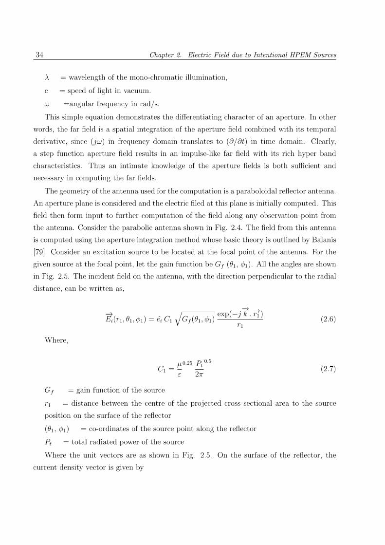
34 Chapter 2. Electric Field due to Intentional HPEM Sources
λ = wavelength of the mono-chromatic illumination,
c = speed of light in vacuum.
ω =angular frequency in rad/s.
This simple equation demonstrates the differentiating character of an aperture. In other
words, the far field is a spatial integration of the aperture field combined with its temporal
derivative, since (jω) in frequency domain translates to (∂/∂t) in time domain. Clearly,
a step function aperture field results in an impulse-like far field with its rich hyper band
characteristics. Thus an intimate knowledge of the aperture fields is both sufficient and
necessary in computing the far fields.
The geometry of the antenna used for the computation is a paraboloidal reflector antenna.
An aperture plane is considered and the electric filed at this plane is initially computed. This
field then form input to further computation of the field along any observation point from
the antenna. Consider the parabolic antenna shown in Fig. 2.4. The field from this antenna
is computed using the aperture integration method whose basic theory is outlined by Balanis
[79]. Consider an excitation source to be located at the focal point of the antenna. For the
given source at the focal point, let the gain function be Gf (θ1, φ1). All the angles are shown
in Fig. 2.5. The incident field on the antenna, with the direction perpendicular to the radial
distance, can be written as,
−→Ei(r1, θ1, φ1) = ei C1
√Gf (θ1, φ1)
exp(−j−→k .−→r1 )
r1(2.6)
Where,
C1 =µ
ε
0.25 Pt2π
0.5
(2.7)
Gf = gain function of the source
r1 = distance between the centre of the projected cross sectional area to the source
position on the surface of the reflector
(θ1, φ1) = co-ordinates of the source point along the reflector
Pt = total radiated power of the source
Where the unit vectors are as shown in Fig. 2.5. On the surface of the reflector, the
current density vector is given by

2.2. Impulse Radiating Antenna 35
−→Js = 2
√ε
µ
√Gf (θ1, φ1)
exp(−j−→k .−→r1 )
r1u (2.8)
The unit vector u can be written from Fig. 2.5 as
ux = −ax sin θ1 sinθ12
cosφ1 (2.9)
uy = ay cosθ12
(sin2 φ1 cos θ1 + cos2 φ1) (2.10)
uz = −az cos θ1 sinθ12
sinφ1 cosφ1 (2.11)
u =ux + uy + uz√
1− sin2 θ1 sin2 φ1
(2.12)
To find the aperture field at a plane through the focal point, the reflected fields Er at r1
is first found. This is of the form
−→Er = er C1
√Gf (θ1, φ1)
exp(−j−→k .−→r1 )
r1(2.13)
Where er is the unit vector depicting the polarization of the field. For the given geometry
er becomes
er =ax sinφ1 cosφ1 (1− cos θ1)− ay (sin2 φ1 cos θ1 + cos2 φ1)√
1− sin2 θ1 sin2 φ1
(2.14)
Hence on any plane passing through the focal point, the reflected field is given by
−→Eap = er C1
√Gf (θ1, φ1)
exp(−j−→k r1 (1 + cos θ1))
r1 (1 + cos θ1)(2.15)
Hence,
−→Eap = ax Eax + ay Eay (2.16)
Where Eax and Eay are the x and y components of the reflected field over the aperture,
and the unit vectors are shown in Fig. 2.5. These aperture fields are a function of the
position along the aperture at which it is computed. These x and y components of the
aperture fields are plotted in Fig. 2.6 and Fig. 2.7 respectively. These plots indicate that
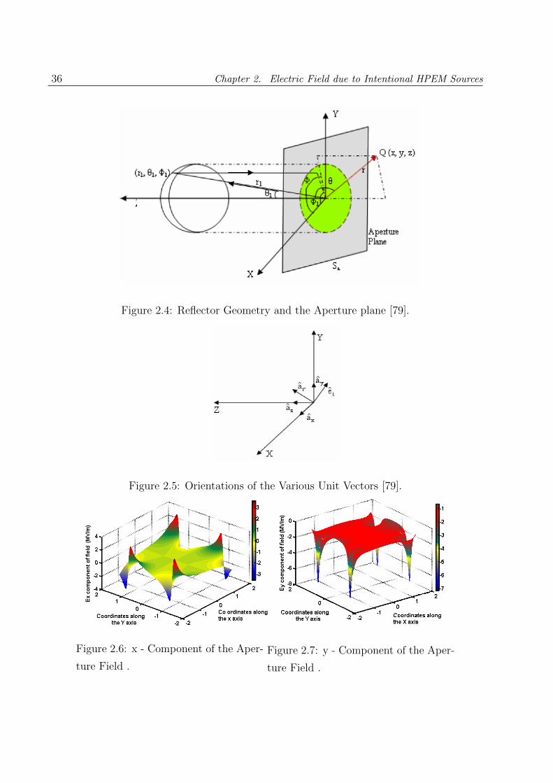
36 Chapter 2. Electric Field due to Intentional HPEM Sources
Figure 2.4: Reflector Geometry and the Aperture plane [79].
Figure 2.5: Orientations of the Various Unit Vectors [79].
Figure 2.6: x - Component of the Aper-
ture Field .
Figure 2.7: y - Component of the Aper-
ture Field .

2.2. Impulse Radiating Antenna 37
the field varies depending upon the co-ordinates along the aperture plane. This necessitates
that to get the total field it is required to carry out an integration of the contribution due
to aperture field at each and every point along the aperture plane, that can be done only
using a numerical integration method which gives proper weightage to the contribution due
to the aperture field at any given point for the computation of the radiated field. From the
general radiation equation, the electric field at any observation point at a distance r from
the focal point can be written as
−→Eθs =
−jk exp(−j−→k .−→r (Lφ + ηNθ)
4πr(2.17)
−→Lφ =
∫∫[−Mx sinφ+My cosφ] exp(−j
−→k .−→r cosψ ds′ (2.18)
Where ψ is the angle between r and r1. Hence the net radiated field is given by
−→Eθs =
−jke(−j−→k .−→r ) (1 + cos θ)
4πr
∫∫(Eax cosφ+ Eay sinφ)ejk (x′ sin θ cosφ+y′ sin θ sinφ)dx′dy′
(2.19)
2.2.2 Radiation Pattern of IRA in the Near and the Far Field
For the JOLT HIRA under consideration, the half paraboloidal antenna [45],has the following
specifications
The diameter, D of the IRA = 3.05 m
The ratio of the focal length, F to the diameter, D = 0.33.
If, λ is the wavelength of the radiated field,then the range at which the far field starts is
a function of the frequency of the radiated field. It can be shown that the far field starts at
df = 2D2
λ(2.20)
The commencement of the far field for different frequencies is tabulated in table 2.1. It
can be seen that the far field starts close to the antenna at 1 MHz, where as it is 61.93 m
if the frequency rises to 1 GHz. To see the effect of this range variation with frequency on
the radiated electric field, the electric field is plotted at two representative distances from
the antenna, one in the near field which is at 5 m and other in the far field of 100 m with

38 Chapter 2. Electric Field due to Intentional HPEM Sources
Table 2.1: Range of Commencement of the Far Field for Different Frequencies of IRA
Frequency The distance of commencement of
(MHz) the far field from IRA (m)
1 0.06
5 3.09
100 6.19
200 12.37
500 30.97
1000 61.93
1500 92.90
10000 618.99
the frequency varied from 1 MHz to 10 GHz. The electric field is computed along the E
plane as a function of the spot frequencies and also with respect to the off boresight angle.
These computations are done with φ assumed to be a constant and the resultant variation
of the field with respect to θ is estimated using equation 2.19 . This field is then normalized
with respect to the maximum electric field intensity occurring along the boresight. The
integration is done numerically in MATLAB along the x and y coordinates of the aperture
plane.
The radiated electric fields are plotted at the spot frequencies of 1 MHz, 50 MHz, 100
MHz, 500 MHz, 1 GHz and 10 GHz for the observation point of 5 m and are shown in Fig.
2.8. The wavelengths for which the computations have been made are 300 m, 6 m, 3 m,
0.6 m, 0.3 m and 0.03 m. The antenna diameter D in terms of wavelength (D/λ) has the
values of 0.01, 0.51, 1.02, 5.08, 10.17 and 101.67. The spot frequencies are 1 MHz, 50 MHz,
500 MHz, 1 GHz, 2 GHz and 10 GHz for the observation point of 100 m and the respective
wavelengths are 300 m, 6 m, 0.6 m, 0.3 m, 0.2 m and 0.03 m respectively. The antenna
diameter D in terms of wavelength (D/λ) has the values of 0.01, 0.51, 1.02, 5.08, 10.17 and
101.67. The change in the spot frequency pattern for 5 m and 100 m is due to the fact
that for the observation point at 5 m, for any frequency after 50 MHz, the field approaches
the far field characteristics whereas for the 100 m point the far field starts only after 1500
MHz. Hence to get the radiated field plots in the far field as well as in the near field, the
frequencies are chosen in the above manner.
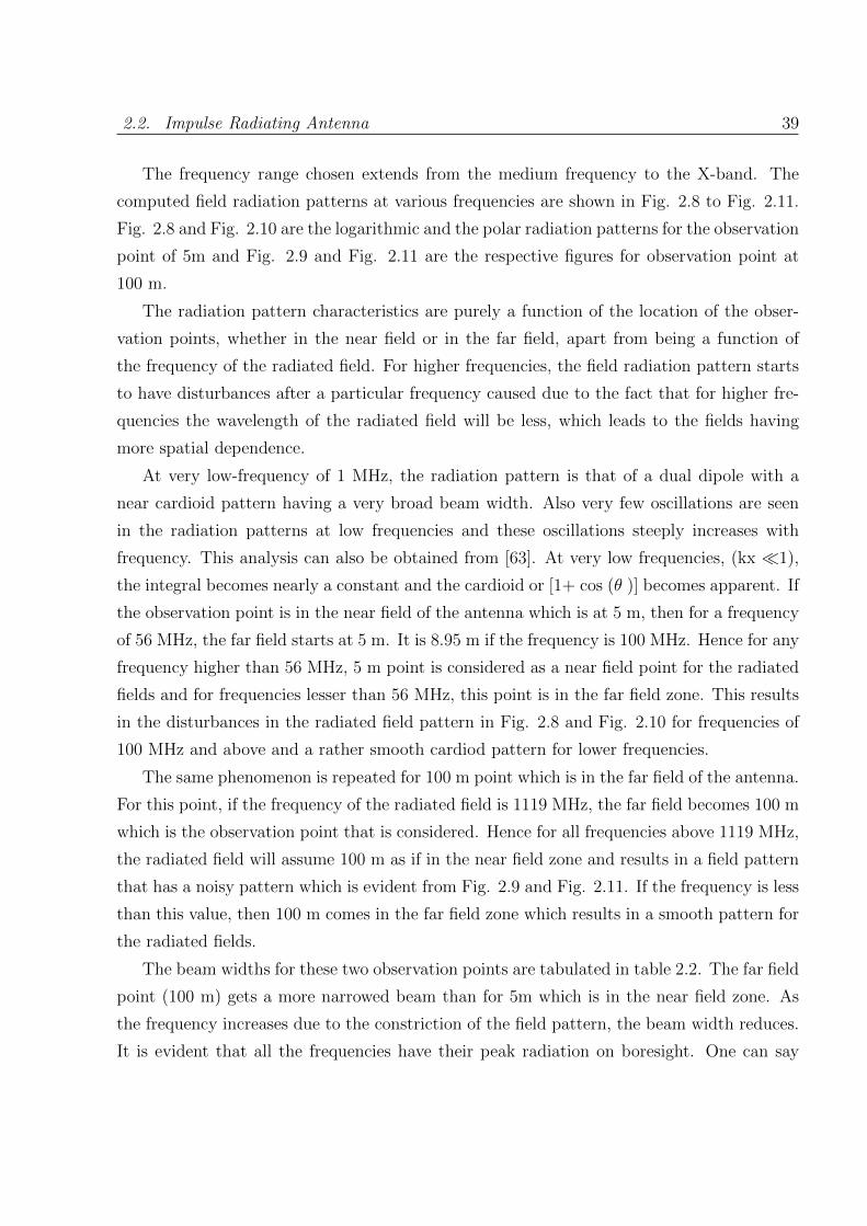
2.2. Impulse Radiating Antenna 39
The frequency range chosen extends from the medium frequency to the X-band. The
computed field radiation patterns at various frequencies are shown in Fig. 2.8 to Fig. 2.11.
Fig. 2.8 and Fig. 2.10 are the logarithmic and the polar radiation patterns for the observation
point of 5m and Fig. 2.9 and Fig. 2.11 are the respective figures for observation point at
100 m.
The radiation pattern characteristics are purely a function of the location of the obser-
vation points, whether in the near field or in the far field, apart from being a function of
the frequency of the radiated field. For higher frequencies, the field radiation pattern starts
to have disturbances after a particular frequency caused due to the fact that for higher fre-
quencies the wavelength of the radiated field will be less, which leads to the fields having
more spatial dependence.
At very low-frequency of 1 MHz, the radiation pattern is that of a dual dipole with a
near cardioid pattern having a very broad beam width. Also very few oscillations are seen
in the radiation patterns at low frequencies and these oscillations steeply increases with
frequency. This analysis can also be obtained from [63]. At very low frequencies, (kx 1),
the integral becomes nearly a constant and the cardioid or [1+ cos (θ )] becomes apparent. If
the observation point is in the near field of the antenna which is at 5 m, then for a frequency
of 56 MHz, the far field starts at 5 m. It is 8.95 m if the frequency is 100 MHz. Hence for any
frequency higher than 56 MHz, 5 m point is considered as a near field point for the radiated
fields and for frequencies lesser than 56 MHz, this point is in the far field zone. This results
in the disturbances in the radiated field pattern in Fig. 2.8 and Fig. 2.10 for frequencies of
100 MHz and above and a rather smooth cardiod pattern for lower frequencies.
The same phenomenon is repeated for 100 m point which is in the far field of the antenna.
For this point, if the frequency of the radiated field is 1119 MHz, the far field becomes 100 m
which is the observation point that is considered. Hence for all frequencies above 1119 MHz,
the radiated field will assume 100 m as if in the near field zone and results in a field pattern
that has a noisy pattern which is evident from Fig. 2.9 and Fig. 2.11. If the frequency is less
than this value, then 100 m comes in the far field zone which results in a smooth pattern for
the radiated fields.
The beam widths for these two observation points are tabulated in table 2.2. The far field
point (100 m) gets a more narrowed beam than for 5m which is in the near field zone. As
the frequency increases due to the constriction of the field pattern, the beam width reduces.
It is evident that all the frequencies have their peak radiation on boresight. One can say

40 Chapter 2. Electric Field due to Intentional HPEM Sources
−150 −100 −50 0 50 100 150−80
−70
−60
−50
−40
−30
−20
−10
0
Angle with respect to boresight(deg.)
Rel
ativ
e el
ectr
ic fi
eld
mag
nitu
de(d
B)
1 MHz.
−150 −100 −50 0 50 100 150−80
−70
−60
−50
−40
−30
−20
−10
0
Angle with respect to boresight(deg.)
Rel
ativ
e el
ectr
ic fi
eld
mag
nitu
de(d
B)
50 MHz.
−150 −100 −50 0 50 100 150−140
−120
−100
−80
−60
−40
−20
0
Angle with respect to boresight(deg.)
Rel
ativ
e el
ectr
ic fi
eld
mag
nitu
de(d
B)
100 MHz.
−150 −100 −50 0 50 100 150−80
−70
−60
−50
−40
−30
−20
−10
0
Angle with respect to boresight(deg.)
Rel
ativ
e el
ectr
ic fi
eld
mag
nitu
de(d
B)
500 MHz.
−150 −100 −50 0 50 100 150
−80
−70
−60
−50
−40
−30
−20
−10
0
Angle with respect to boresight(deg.)
Rel
ativ
e el
ectr
ic fi
eld
mag
nitu
de(d
B)
1000 MHz.
−150 −100 −50 0 50 100 150
−100
−80
−60
−40
−20
0
Angle with respect to boresight(deg.)
Rel
ativ
e el
ectr
ic fi
eld
mag
nitu
de(d
B)
10000 MHz.
Figure 2.8: Logarithmic Plot of Antenna Radiation Pattern at 5 m.

2.2. Impulse Radiating Antenna 41
−150 −100 −50 0 50 100 150−80
−70
−60
−50
−40
−30
−20
−10
0
Angle with respect to boresight (deg.)
Rel
ativ
e el
ectr
ic fi
eld
mag
nitu
de
(dB
)
1 MHz.
−150 −100 −50 0 50 100 150
−80
−70
−60
−50
−40
−30
−20
−10
0
Angle with respect to boresight (deg.)
Rel
ativ
e el
ectr
ic fi
eld
mag
nitu
de (
dB)
50 MHz.
−150 −100 −50 0 50 100 150−100
−80
−60
−40
−20
0
Angle with respect to boresight (deg.)
Rel
ativ
e el
ectr
ic fi
eld
mag
nitu
de (
dB)
500 MHz.
−150 −100 −50 0 50 100 150−100
−80
−60
−40
−20
0
Angle with respect to boresight (deg.)
Rel
ativ
e el
ectr
ic fi
eld
mag
nitu
de
(dB
)
1000 MHz.
−150 −100 −50 0 50 100 150−100
−80
−60
−40
−20
0
Angle with respect to boresight (deg.)
Rel
ativ
e el
ectr
ic fi
eld
mag
nitu
de (
dB)
2000 MHz.
−150 −100 −50 0 50 100 150−100
−80
−60
−40
−20
0
Angle with respect to boresight (deg.)
Rel
ativ
e el
ectr
ic fi
eld
mag
nitu
de (
dB)
10000 MHz.
Figure 2.9: Logarithmic Plot of Antenna Radiation Pattern at 100 m.
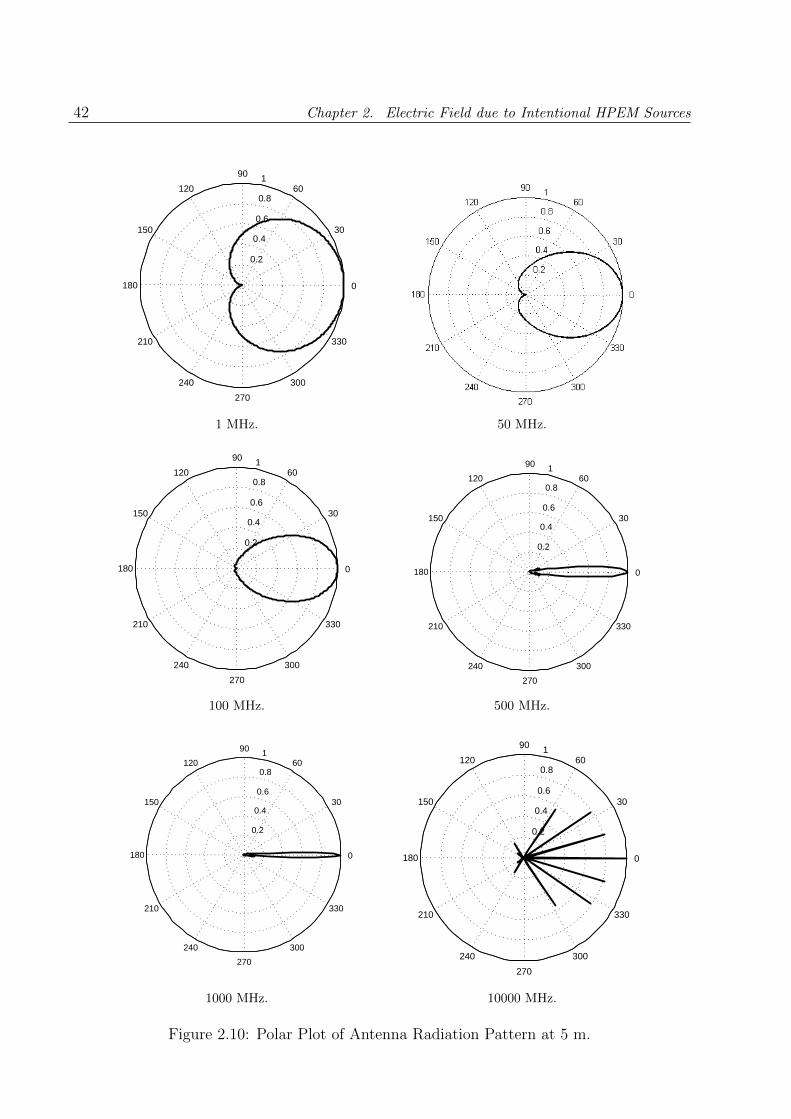
42 Chapter 2. Electric Field due to Intentional HPEM Sources
0.2
0.4
0.6
0.8
1
30
210
60
240
90
270
120
300
150
330
180 0
1 MHz. 50 MHz.
0.2
0.4
0.6
0.8
1
30
210
60
240
90
270
120
300
150
330
180 0
100 MHz.
0.2
0.4
0.6
0.8
1
30
210
60
240
90
270
120
300
150
330
180 0
500 MHz.
0.2
0.4
0.6
0.8
1
30
210
60
240
90
270
120
300
150
330
180 0
1000 MHz.
0.2
0.4
0.6
0.8
1
30
210
60
240
90
270
120
300
150
330
180 0
10000 MHz.
Figure 2.10: Polar Plot of Antenna Radiation Pattern at 5 m.
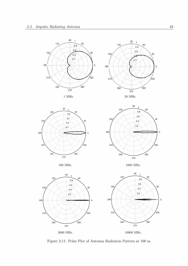
2.2. Impulse Radiating Antenna 43
1 MHz. 50 MHz.
0.2
0.4
0.6
0.8
1
30
210
60
240
90
270
120
300
150
330
180 0
500 MHz.
0.2
0.4
0.6
0.8
1
30
210
60
240
90
270
120
300
150
330
180 0
1000 MHz.
0.2
0.4
0.6
0.8
1
30
210
60
240
90
270
120
300
150
330
180 0
2000 MHz.
0.2
0.4
0.6
0.8
1
30
210
60
240
90
270
120
300
150
330
180 0
10000 MHz.
Figure 2.11: Polar Plot of Antenna Radiation Pattern at 100 m.

44 Chapter 2. Electric Field due to Intentional HPEM Sources
that this is somewhat fortuitous, since when this antenna was originally designed, the low
frequency performance has not been considered. Later analyses showed that even at very
low frequencies where the antenna can be characterized by a pair of dipole moments (electric
and magnetic), the resultant radiation is in the boresight direction.
The field patterns at various frequencies shown in Fig. 2.8 Fig. 2.11are just that they
are not indicative of the relative strength of the fields at various frequencies, but only the
variation in the off boresight axis, after normalizing the fields to the peak value on boresight
at each frequency. The relative strengths of each sinusoidal component and the relative
phases depend on many factors such as the excitation voltage spectrum, antenna size etc.
The directive gain or the gain along the boresight of the IRA as a function of frequency is
easy to derive.
Table 2.2: Beam Width as a Function of Frequency for Different Distances
Frequency Bandwidth (Deg.) Bandwidth (Deg.)
(MHz) for 5m for 100m
1 131 124
50 95 90
100 47 45
200 24 20
500 9.5 9
1000 4.8 4
1500 2.5 2
10000 1.5 1
On the boresight, the directive gain becomes
G = limr→∞
[4πZinZ0
] [rE
Va]2 (2.21)
Where Va is the voltage input. In the far field r →∞
rE
Va=
D
2λfg2(2.22)
G =πD2
fg2λ2
(2.23)

2.2. Impulse Radiating Antenna 45
Where D is the reflector diameter and fg2 = Zin/Zo. For a 2-arm IRA, the numerical
parameters are D=3.66 m and fg2 = 400 Ω / 377 Ω = 1.061, and its directive gain is listed
in table 2.3.
Table 2.3: Estimated Directive Gain vs. Frequency for a 2-arm IRA (same as for a 4-arm
IRA)
Frequency Wavelength, D/λ Directive Gain Directive Gain
(MHz) λ (m) (Numerical) dB
1 300 0.01 4.2 x 10⁻⁴ -67.5
50 6 0.61 1.1 -0.8
100 3 1.22 4.4 12.9
200 1.5 2.44 17.6 24.9
500 0.6 6.10 110 40.9
1000 0.3 12.21 442 52.9
1500 0.2 18.30 991 59.9
10000 0.03 122.00 44048 92.9
The gain is seen to increase as (frequency) 2 or 20 dB per decade. In practice, however,
the gain does not arbitrarily increase and will cut off at some high frequency due to feed
imperfections. It is also observed that for a 4-arm IRA, the radiated field is larger by a factor
of√
2 resulting in twice the radiated power of a 2-arm IRA. But, in this case the input power
is also increased by a factor of 2. Consequently, the directive gain remains unchanged. The
gains of the aperture antennas are summarised in table 2.4.
2.2.3 Illustrative Example in Time Domain
To get the temporal characteristics of the JOLT IRA, the reflector is considered to be fed by
a transverse electromagnetic wave structure energized by a pulser source. This source has
the following characteristics [45]:
The far field electric field measured in the boresight at r = 85 m being equal to 62 kV/m,
The uncorrected pulse rise time (10%-90%) equal to 180 ps.
This parabolic IRA reflector is shown in the Fig. 2.12. The following analytical model
has been used to describe the output voltage, according to which the pulser output voltage,
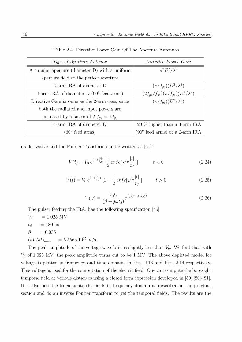
46 Chapter 2. Electric Field due to Intentional HPEM Sources
Table 2.4: Directive Power Gain Of The Aperture Antennas
Type of Aperture Antenna Directive Power Gain
A circular aperture (diameter D) with a uniform π2D2/λ2
aperture field or the perfect aperture
2-arm IRA of diameter D (π/fg2)(D2/λ2)
4-arm IRA of diameter D (900 feed arms) (2fg4/fg2)(π/fg2)(D2/λ2)
Directive Gain is same as the 2-arm case, since (π/fg2)(D2/λ2)
both the radiated and input powers are
increased by a factor of 2 fg2 = 2fg4
4-arm IRA of diameter D 20 % higher than a 4-arm IRA
(600 feed arms) (900 feed arms) or a 2-arm IRA
its derivative and the Fourier Transform can be written as [61]:
V (t) = V0 e(−β |t|
td)[1
2erfc(
√π|t|td
)] t < 0 (2.24)
V (t) = V0 e(−β |t|
td)[1− 1
2erfc[
√π|t|td
]] t > 0 (2.25)
V (ω) =V0td
(β + jωtd)e
14π
(β+jωtd)2
(2.26)
The pulser feeding the IRA, has the following specification [45]
V0 = 1.025 MV
td = 180 ps
β = 0.036
(dV/dt)max = 5.556×10¹⁵ V/s.
The peak amplitude of the voltage waveform is slightly less than V0. We find that with
V0 of 1.025 MV, the peak amplitude turns out to be 1 MV. The above depicted model for
voltage is plotted in frequency and time domains in Fig. 2.13 and Fig. 2.14 respectively.
This voltage is used for the computation of the electric field. One can compute the boresight
temporal field at various distances using a closed form expression developed in [59],[80]-[81].
It is also possible to calculate the fields in frequency domain as described in the previous
section and do an inverse Fourier transform to get the temporal fields. The results are the

2.2. Impulse Radiating Antenna 47
same and the spectral and temporal fields are plotted in Fig. 2.15 and Fig. 2.17 respectively
which are computed from the aperture integration method of the previous section combined
with Fourier inversion. The far field can be shown to start at a range r given by [45]
r ≥ D2
2ctd(2.27)
This range turns out to be 85 m. The computation have been validated by comparing it
with the measured electric field at the observation point at a boresight range of 304 m. The
measured electric field at this observation point as taken from the literature [45] are shown
in Fig. 2.16 and Fig. 2.18 which shows a close similarity with the computed results.
2.2.4 Equivalence between Spectral and Temporal Characteristics
of IRA
The equivalence is based on the fundamental principle of Fourier or Laplace transformation.
For simplicity, let us write the Fourier transform pair of integrals.
f(t) =1
2π
+∞∫−∞
F (ω)ejωtdω (2.28)
F (ω) =
+∞∫−∞
f(t)e−jωtdt (2.29)
Note that is a real function of a real variable t while F (ω) is a complex function of
a real variable . One has to know the temporal function for all times to get the spectrum
and conversely, one has to know the spectral function for all frequencies to get the temporal
function. In measurement scenarios, this creates a problem since the data is either band
limited or time limited. Nevertheless the equivalence is straight forward. By setting t = 0
and ω = 0, observe that
f(0) =1
2π
+∞∫−∞
F (ω)dω (2.30)
F (0) =
+∞∫−∞
f(t)dt (2.31)
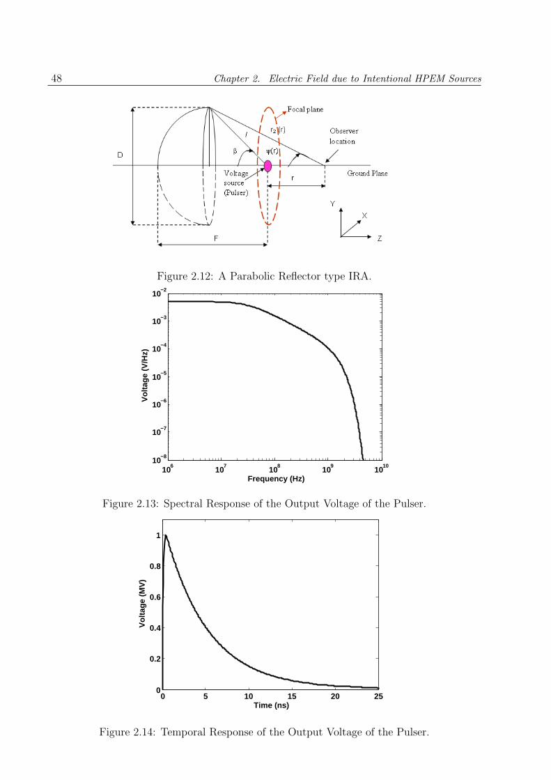
48 Chapter 2. Electric Field due to Intentional HPEM Sources
Figure 2.12: A Parabolic Reflector type IRA.
106
107
108
109
1010
10−8
10−7
10−6
10−5
10−4
10−3
10−2
Frequency (Hz)
Vol
tage
(V
/Hz)
Figure 2.13: Spectral Response of the Output Voltage of the Pulser.
0 5 10 15 20 250
0.2
0.4
0.6
0.8
1
Time (ns)
Vo
ltag
e (M
V)
Figure 2.14: Temporal Response of the Output Voltage of the Pulser.

2.2. Impulse Radiating Antenna 49
106
107
108
109
1010
10−9
10−8
10−7
10−6
10−5
10−4
Frequency (Hz)
Ele
tric
fiel
d in
tens
ity (
V/m
/Hz)
40m60m80m100m200m
Figure 2.15: Spectral Response of the
Radiated Electric Field from the IRA at
Different Distances along the Boresight.
Figure 2.16: Frequency Domain Wave-
form of the Measured Field from the
JOLT IRA along the Boresight at a dis-
tance of 304 m [45].
0 1 2 3 4 5 6 7 8
0
50
100
150
Time (ns)
Ele
ctri
c fi
eld
inte
nsi
ty (
kV/m
)
40m60m80m100m200m
Figure 2.17: Temporal Response of
the Radiated Electric Field from the
IRA at Different Distances Along the
Boresight.
Figure 2.18: Time Domain Waveform of
the Measured Field from a JOLT IRA
Along the Boresight at a distance of 304
m [45].
50 Chapter 2. Electric Field due to Intentional HPEM Sources
Both of these quantities (initial value in time domain and DC content in frequency
domain) need to be zero if we are dealing with a radiated electric field. The reasons being;
1) there cannot be a radiated signal before the signal can get there and 2) antennas do not
radiate DC into the far field. Ensuring these vanishing quantities in a measurement can be
a good check on the measurement schemes. In the context of an IRA, it is observed that it
can be excited by a transient pulse that contains many frequencies or by a single frequency
sinusoidal voltage. If we apply a CW sinusoidal voltage to the IRA, the far field is the
derivative of the sinusoid or simply a co-sinusoid everywhere. What is changing with the
observer location is the amplitude and phase of that co-sinusoid. The amplitude is changing
with the off boresight angle as is estimated in Fig. 2.8 to Fig. 2.11 at various frequencies.
The amplitude on the boresight will depend on the antenna size, frequency and the antenna
impedance. If we use the IRA in a pulsed mode, the voltage pulse has many frequencies.
They all get radiated from the same focal point of the reflector (hence the antenna is non-
dispersive). However, each frequency has a different radiation pattern as shown in Fig. 2.8
to Fig. 2.11 at various frequencies . If we measure the radiated field at any arbitrary position
in front of the antenna, we get a temporal waveform of the field, as in Fig. 2.16. This has
a definite relationship with the applied voltage. It is important to realize that this field
when Fourier transformed will have many frequencies with varying amplitudes and phases.
Phase is a frequency domain concept and is equivalent to a delay in time domain. A time
domain signal, radiated electric field as in the case of Fig. 2.16, is merely a collection of
many sinusoids, each with a different amplitude and phase.
Gain and beam-width of the IRA is calculated in section 3 as a function of the frequency.
In time domain the precise definitions of gain and beam-width are yet to be standardized.
We have chosen to define the temporal beam-width as the angular points where the peak
power of the temporal waveforms is 70%of their boresight value. This is simply a matter of
convenience at this time. Suffice it to say that in front of the pulse-excited IRA, one has a
temporal waveform of the electric field at any arbitrary observation point and this waveform
can be Fourier transformed to observe its spectral content. It does not make sense to talk
of side lobes in time domain. One can also assert that the high frequencies have the highest
directive gain and hence the pulse on boresight will have the shortest rise time. The radiated
pulse becomes smaller and fatter as, one goes off the boresight. It is likely that standardized
definitions of gain and beam-width will evolve in the future for pulsed antennas.

2.3. Electric Field at the Different Points due to a HPM Source 51
2.3 Electric Field at the Different Points due to a HPM
Source
In the present study, a single waveguide (type WR-975) fed HPM antenna assembly has
been considered. The dimensions of this waveguide are a = 247.65 mm and b = 123.83 mm
having a propagation frequency of 1 GHz and nominal frequency range of 0.75-1.12 GHz
[71]-[77]. The peak electric field in the waveguide is taken as 25 MV/m. The spectral and
temporal response of the waveguide field is plotted in Fig. 2.19 and Fig. 2.20.
This has a cut-off frequency of 1 GHz and a power level of 10 GW. The wavelength
associated with the waveguide is 0.3 m. The field pattern shows a definite peak in its
response when the frequency is 1 GHz, the cut-off frequency of the waveguide. On the lower
side of the cut-off frequency, the field magnitude is constant and on the higher side it sharply
drops as the frequency increases. The average power, Pavg in the rectangular waveguide is
[71]-[77].
Pavg =E2
0
2ζ0
ab
2(1− λ
2a2)0.5 (2.32)
where
E0 = peak electric field in the waveguide
ζ0 = characteristic impedance of the free space
λ = operating wavelength
a = inside larger dimension of the waveguide
b = inside smaller dimension of the waveguide
Hence the peak electric field, Epeak in the waveguide can be written as
Epeak = E0 =√
2pavgz1,0 (2.33)
where
z1,0 = ζ0 (1− λ
2a2)0.5 (2.34)
Because of its dominant H1,0 mode of propagation, the field will have only that component
and all other components will be zero in this mode of propagation. The power in this
waveguide is fed to the evacuated pyramidal feed horn. The peak electric field intensity in
the horn aperture is given by,

52 Chapter 2. Electric Field due to Intentional HPEM Sources
Epeak(horn) = Epeak(waveguide)ab
a′b′(2.35)
where,
a = the width of the horn
b = the height of the horn
Hence the net field along the aperture will be given by,
Ex = Epeak(horn) cosπy
ae−jk[ x
′22lE
+ y′22lH
](2.36)
The field along the aperture of the horn depicted by the above equation is a function
of the distance from the centre of the horn. This field is plotted in Fig. 2.21. This figure
shows bell type characteristics that peak at the centre of the horn with no variation along
its width. Since the aperture field is a function of the coordinates along the aperture of the
pyramidal horn, it is non-uniform in nature. This is typical of the H1,0 mode of propagation.
The peak electric field intensity is 2.93 MV/m. The waveguide field response also has an
identical characteristics and the response is given by equation 2.33. This aperture field serves
as an input parameter for computing the field from the pyramidal horn antenna. The output
field from the horn antenna can be either in a reactive near field, radiating intermediate field
or Fresnel region and in a radiating far field or Fraunhofer region. The Fresnel region is
important to analyze the dielectric interface required at the reflector so that there is no
breakdown occurring at the region close to the reflector. Fraunhofer fields are the basic
source in the assessment of the reflector illumination.
The electric field from a pyramidal horn antenna at any distance r from it can be written
as:
−→E (x, y, z) =
1
4π
∫∫ −→E (x′, y′) e
−jkrr [(jk +
1
r) cos θ + jk] dx′ dy′ (2.37)
Where E (x′, y′) is the aperture field, Ex that is obtained from equation 2.36. θ is the
angle off the boresight at the observation point considered. A non uniform aperture field
causes the integrand to be evaluated at each and every points, hence numerical integration
is required to tackle this situation. This field of the pyramidal horn antenna serves as input
to the offset Cassegrain reflector antenna. Using equation 2.37 the net field at the reflector
input can be computed and this field forms the input for determining the radiated field
output from the reflector antenna.

2.3. Electric Field at the Different Points due to a HPM Source 53
106
107
108
109
1010
10−20
10−15
10−10
10−5
100
Frequency (Hz)
Ele
ctric
fiel
d in
tens
ity m
agni
tude
(V
/m/H
z)
Figure 2.19: Spectral Response of the Electric Field in the Waveguide.
0 1 2 3 4 5−15
−10
−5
0
5
10
15
20
25
Time (ns)
Ele
ctric
fiel
d (M
V/m
)
Figure 2.20: Time Response of the Electric Field in the Waveguide.
01
23
4
0
5
100
1
2
3
Distance along the width (m)
Distance along the height (m)
E−f
ield
(M
V/m
)
0.5
1
1.5
2
2.5
Figure 2.21: The Aperture Field Distribution.

54 Chapter 2. Electric Field due to Intentional HPEM Sources
For the present work the parameters of the horn and the reflector are [71]-[78]: horn
aperture height = 3.5λ and reflector area = 20 m2. The peak electric field at the horn
aperture is obtained as 2.93 MV/m from Fig. 2.21. The peak field at the reflector surface
came out to be 335 kV/m, as per 2.35. Using this field, the radiated field output at 100
m from the antenna assembly is plotted in Fig. 2.22 and Fig. 2.23 in frequency and time
domains. The mesh plot of the electric field is shown in Fig. 2.24
These figures bring out the fact that the field is dominant at 1 GHz, the cut-off frequency
of the waveguide. The maximum field is 410 kV/m and the delay time of 333 ns corresponds
to the travel time from the antenna to the observation point.
2.4 Chapter Summary
The electric field is computed at different points from the HPEM sources, based on the
characteristic properties of the sources. NEMP field at earths surface is modeled using
the IEC standard 61000-2-9. The radiation pattern is calculated for the IRA using the
aperture integration using the aperture field which is shown in the chapter. The HPM field
is computed at the observation point using the non uniform aperture field. The following
inferences are arrived at:
• The electric field at any point is a function of the type of the source and the charac-
teristics of the source.
• The maximum electric field occurs at the boresight.
• For an IRA, the shape of the radiation pattern of the electric field is decided by the
frequency, and also whether the observation point is in the near or the far field with
respect to the antenna.
• Polar plot of the radiation pattern has no side lobes till the frequency is 50 MHz if the
observation point is at 5m but after wards it changes to irregular patterns with side
lobes. Polar plot is having no sidelobes till 1500 MHz if the observation point changes
to 100 m. This is decided by the range of commencement of the far field for a given
frequency.
• Beam width of the radiation pattern decreases with an increase in the frequency for
any observation point.

2.4. Chapter Summary 55
106
107
108
109
1010
10−20
10−15
10−10
10−5
100
Frequency (Hz)
Ele
ctric
fiel
d in
tens
ity m
agni
tude
(V
/m/H
z)
Figure 2.22: Spectral Response of the Electric Field due to HPM Source at Different Points
at 100 m Away From the Source.
358 360 362 364 366 368−300
−1000
100
300
500
Time (ns)
Ele
ctric
fiel
d (K
V/m
)
346 348 350 352 354 356−300
−1000
100
300
500
Time (ns)
Ele
ctric
fiel
d (K
V/m
)
330 335 340−300
−1000
100
300
500
Time (ns)
Ele
ctric
fiel
d (K
V/m
)
358 360 362 364 366 368−300
−1000
100
300
500
Time (ns)
Ele
ctric
fiel
d (K
V/m
)
Figure 2.23: Time Response of the Electric Field due to HPM Source at Different Points at
100 m Away From the Source.
Figure 2.24: Mesh Plot of the Time Response of the Electric Field due to HPM Source at
Different Points at 100 m Away from the Source.

56 Chapter 2. Electric Field due to Intentional HPEM Sources
• The gain of the antenna increases as square of the frequency with each increase in the
frequency.
• The electric field at the boresight of an IRA has a prepulse that lasts for 8 ns which
accounts for the time taken by the pulse to traverse the reflector diameter before it is
felt at the given observation point.
• For an HPM, the field has a centre frequency of 1 GHz, which is the centre frequency
of the waveguide field.
• The aperture field along the pyramidal horn antenna is mainly cosine in nature with
a maximum field at the centre of the horn cross section.
• The electric field at any observation point is decided by the dimensions of the horn,
the dimension of the reflector antenna that finally radiates the field and also the char-
acteristics of the waveguide field.
Chapter 3
Influence of the Medium on the
Electric field Propagation
The electric field coming out of the HPEM sources travels through the media that could be
either air alone or a combination of air and soil respectively depending upon whether the
system on which the EM coupling process is analysed is an airborne vehicle or an underground
cable. The intervening medium plays a major role in the coupling process and the magnitude
of the coupled field is influenced by the characteristic properties of the medium. This chapter
deals with the effect of the air medium as well as the combination of air and soil media on
the electric field coming out of these sources.
3.1 Electric Field in Different Media due to HPEM
Sources
The electric field reaching the earth’s surface will suffer reflection from the earth and only a
percentage of the incoming field will be able to penetrate into the soil. This percentage of the
field transmitted into the soil is a function of the characteristic properties of the soil. The soil
is characterized by its dielectric permittivity and conductivity. To quantify the above soil
parameters two coefficients are used which actually determines the exact magnitude of the
field either in soil or in the air. These are the earth’s reflection and transmission coefficients
known as the Fresnel coefficients. A schematic diagram for field propagation in air or soil is
shown in Fig. 3.1.
The electric field at any height, h above the earth can hence be written as:
E(x, 0, h) = Einc + Eref (3.1)
57

58 Chapter 3. Influence of the Medium on the Electric field Propagation
Figure 3.1: Schematic Diagram for Field Propagation Air and Soil.
where
Eref = EincRv (x sinψ cosφ + y sinψ sinφ + z cosψ)ejk(−x cosψ cosφ+y cosψ sinφ−z sinψ) (3.2)
and Rv is the Fresnel reflection coefficient, which can be written as [95]
Rv =((εr(1 + σg
jωε0εr) sinψ)− (εr(1 + σg
jωε0εr))− cos2 ψ)0.5
((εr(1 + σgjωε0εr
) sinψ) + (εr(1 + σgjωε0εr
))− cos2 ψ)0.5(3.3)
Here Einc is the incident field due to HPEM sources, either in time or frequency domain.
These fields are given in detail in the previous chapter. ψ and φ are the angles of incidence,
εr is the relative permittivity of the soil and σg is its conductivity. Similarly at any depth d
below the soil, the net field will be due to the field transmitted into the soil, which can be
written as
E(x, 0, d) = Et (3.4)
where
Eref = EincTv (x sinψt cosφ − y sinψt sinφ + z cosψ)ejk(−x cosψt cosφ+y cosψt sinφ−z sinψ) (3.5)
Where Tv is the Fresnel transmission coefficient, which can be written as [95]

3.2. Electric Field in Air at Varied Heights due to HPEM Sources 59
Tv =2Z0g sinψ
Z0 sinψ + Z0g sinψt(3.6)
sinψt =
√1 + (
k cosψ
γg)2 (3.7)
Here is the transmitted angle which is a function of the characteristic properties of the
soil. All these angles are shown in the Fig. 3.1. These Fresnel reflection and transmission
coefficients are a function of the angles of incidence of the field with the earth’s surface.
These coefficients are plotted as a function of the angles of incidence in Fig. 3.2 to Fig. 3.4.
The values of the reflection and the transmission coefficients approaches a constant value
asymptotically, such that their sum is equal to 1.This constant value is 0.53 if the angle of
incidence is 900, and the transmission coefficient approaches asymptotically to 0.47 at this
same angle of incidence.
3.2 Electric Field in Air at Varied Heights due to HPEM
Sources
The electric field at the earth’s surface due to a high altitude nuclear electromagnetic pulse
is taken 50 kV/m according to the standard. Using this field at the earth’s surface, the
electric field at any height above the earth’s surface can be obtained after getting the earth’s
reflection coefficient at the frequencies of interest of NEMP. The NEMP field as a function
of frequency and item is plotted in Fig. 3.5 and Fig. 3.6. As height increases the field drops
29 kV/m to 3 kV/m as the height increases from 100 m to 1000 m in steps of 100 m. The
shift in the time domain is a function of the height at which the field is computed. The IRA
field at different heights is plotted in frequency and time domain for the source discussed
in section 2.2.2 in Fig. 3.7 and Fig. 3.8 respectively. The field varies from 24.8 kV/m to 5
kV/m for the above height range with the time delay a function of the height. The HPM
field shows a variation from 160 kV/m to 20 kV/m for this height range as can be seen from
Fig. 3.9 and Fig. 3.10.
The variation of the field with height is a function of the type of the source and also the
characteristics of the medium which is air. The frequency domain waveforms for the field
at different heights for these sources show that as the source varies from NEMP to IRA to

60 Chapter 3. Influence of the Medium on the Electric field Propagation
Figure 3.2: Fresnel Vertical Reflection Coefficient, Rv.
Figure 3.3: Fresnel Vertical Transmission Coefficient,Tv .
106
107
108
109
1010
0.35
0.4
0.45
0.5
0.55
0.6
0.65
0.7
Frequency (Hz)
Fre
snel
co
effi
cien
ts
Vertical reflectioncoefficient
Vertical transmissioncoefficient
Figure 3.4: Fresnel Vertical Reflection and Transmission Coefficients for an Incident Angle
of 900.

3.3. Electric Field Attenuation due to Soil Characteristics 61
HPM, the variation in the magnitude of the fields with height is less noticable, which means
the graphs are more crowded at higher heights.
3.3 Electric Field Attenuation due to Soil Character-
istics
The electric field from the sources of HPEM has to travel through soil medium before it
encounters with the buried cable. Hence the characteristics of the field at the cable are
largely dependent upon the electrical and magnetic characteristics of the soil. But electrical
parameters are more important than the magnetic properties for coupling studies. As such,
it is worthwhile to analyse the effect of the soil electrical parameters on the electric field
intensity due to different HPEM sources. The equation given in section 3.1 can be used for
the determination of the electric field in the soil.
3.3.1 Effect of Soil Parameters on the Electric Field
The electric field reaching the soil will suffer attenuation once it enters the soil due to
the effect of the soil properties. When the field passes through the soil, the amount of the
attenuation it suffers can be mathematically represented in terms of the attenuation constant
of the soil. The attenuation constant is the real part of the complex propagation constant.
Fig. 3.11 and Fig. 3.12 show the attenuation constant and the phase constant as a function
of the frequency contents in the field, for different electrical conductivities of the soil. The
attenuation constant rises linearly with frequency at low frequencies and reaches a constant
value asymptotically at higher frequencies. The point at which this shift in the attenuation
from linearity to steady state increases as the soil conductivity increases which are 5 MHz,
10 MHz, 100 MHz, 1 GHz and 10 GHz respectively for conductivities 0.001 S/m to 10 S/m.
So with every 10 times increase in conductivity, the change over frequency also shifts by 10
times. The attenuation coefficient is dependent upon the nature of the soil and the energy of
the incoming electromagnetic field. If the energy of the incoming electromagnetic radiation
is higher on account of the higher energy of the incident photons, and if the material is less
dense, then lower will be the attenuation coefficient. The phase constant follows a linear
variation with frequency but has two linear variations, the initial one having a slope of
3.5/decade for the conductivity of the soil of 1 S/m, but finally approaches asymptotically
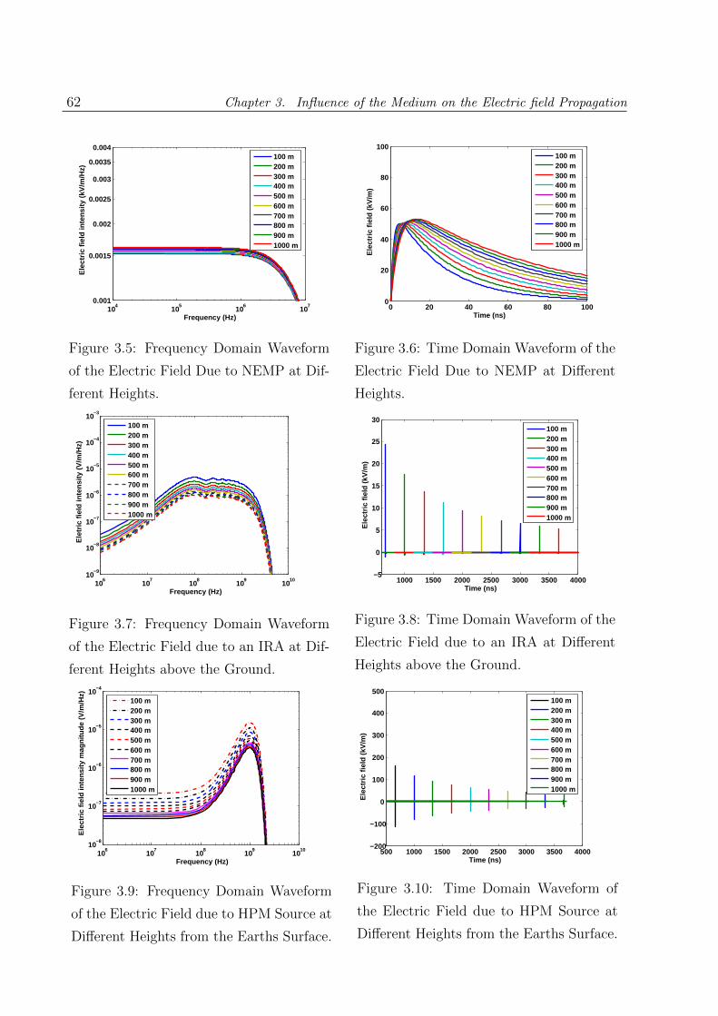
62 Chapter 3. Influence of the Medium on the Electric field Propagation
104
105
106
107
0.001
0.0015
0.002
0.0025
0.003
0.0035
0.004
Frequency (Hz)
Ele
ctri
c fi
eld
inte
nsi
ty (
kV/m
/Hz)
100 m200 m300 m400 m500 m600 m700 m800 m900 m1000 m
Figure 3.5: Frequency Domain Waveform
of the Electric Field Due to NEMP at Dif-
ferent Heights.
0 20 40 60 80 1000
20
40
60
80
100
Time (ns)
Ele
ctri
c fi
eld
(kV
/m)
100 m200 m300 m400 m500 m600 m700 m800 m900 m1000 m
Figure 3.6: Time Domain Waveform of the
Electric Field Due to NEMP at Different
Heights.
106
107
108
109
1010
10−9
10−8
10−7
10−6
10−5
10−4
10−3
Frequency (Hz)
Ele
tric
fiel
d in
tens
ity (
V/m
/Hz)
100 m200 m300 m400 m500 m600 m700 m800 m900 m1000 m
Figure 3.7: Frequency Domain Waveform
of the Electric Field due to an IRA at Dif-
ferent Heights above the Ground.
1000 1500 2000 2500 3000 3500 4000−5
0
5
10
15
20
25
30
Time (ns)
Ele
ctric
fiel
d (k
V/m
)
100 m200 m300 m400 m500 m600 m700 m800 m900 m1000 m
Figure 3.8: Time Domain Waveform of the
Electric Field due to an IRA at Different
Heights above the Ground.
106
107
108
109
1010
10−8
10−7
10−6
10−5
10−4
Frequency (Hz)
Ele
ctric
fiel
d in
tens
ity m
agni
tude
(V
/m/H
z) 100 m200 m300 m400 m500 m600 m700 m800 m900 m1000 m
Figure 3.9: Frequency Domain Waveform
of the Electric Field due to HPM Source at
Different Heights from the Earths Surface.
500 1000 1500 2000 2500 3000 3500 4000−200
−100
0
100
200
300
400
500
Time (ns)
Ele
ctric
fiel
d (k
V/m
)
100 m200 m300 m400 m500 m600 m700 m800 m900 m1000 m
Figure 3.10: Time Domain Waveform of
the Electric Field due to HPM Source at
Different Heights from the Earths Surface.
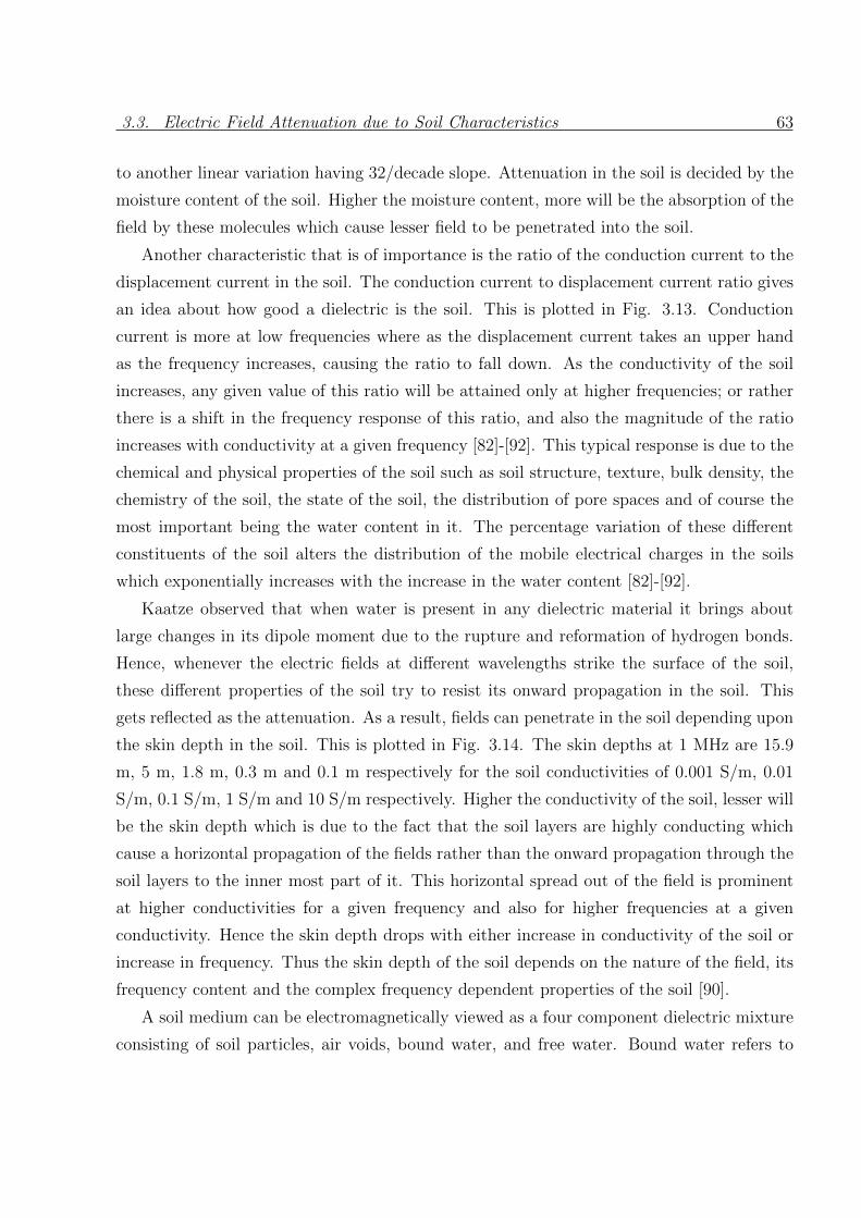
3.3. Electric Field Attenuation due to Soil Characteristics 63
to another linear variation having 32/decade slope. Attenuation in the soil is decided by the
moisture content of the soil. Higher the moisture content, more will be the absorption of the
field by these molecules which cause lesser field to be penetrated into the soil.
Another characteristic that is of importance is the ratio of the conduction current to the
displacement current in the soil. The conduction current to displacement current ratio gives
an idea about how good a dielectric is the soil. This is plotted in Fig. 3.13. Conduction
current is more at low frequencies where as the displacement current takes an upper hand
as the frequency increases, causing the ratio to fall down. As the conductivity of the soil
increases, any given value of this ratio will be attained only at higher frequencies; or rather
there is a shift in the frequency response of this ratio, and also the magnitude of the ratio
increases with conductivity at a given frequency [82]-[92]. This typical response is due to the
chemical and physical properties of the soil such as soil structure, texture, bulk density, the
chemistry of the soil, the state of the soil, the distribution of pore spaces and of course the
most important being the water content in it. The percentage variation of these different
constituents of the soil alters the distribution of the mobile electrical charges in the soils
which exponentially increases with the increase in the water content [82]-[92].
Kaatze observed that when water is present in any dielectric material it brings about
large changes in its dipole moment due to the rupture and reformation of hydrogen bonds.
Hence, whenever the electric fields at different wavelengths strike the surface of the soil,
these different properties of the soil try to resist its onward propagation in the soil. This
gets reflected as the attenuation. As a result, fields can penetrate in the soil depending upon
the skin depth in the soil. This is plotted in Fig. 3.14. The skin depths at 1 MHz are 15.9
m, 5 m, 1.8 m, 0.3 m and 0.1 m respectively for the soil conductivities of 0.001 S/m, 0.01
S/m, 0.1 S/m, 1 S/m and 10 S/m respectively. Higher the conductivity of the soil, lesser will
be the skin depth which is due to the fact that the soil layers are highly conducting which
cause a horizontal propagation of the fields rather than the onward propagation through the
soil layers to the inner most part of it. This horizontal spread out of the field is prominent
at higher conductivities for a given frequency and also for higher frequencies at a given
conductivity. Hence the skin depth drops with either increase in conductivity of the soil or
increase in frequency. Thus the skin depth of the soil depends on the nature of the field, its
frequency content and the complex frequency dependent properties of the soil [90].
A soil medium can be electromagnetically viewed as a four component dielectric mixture
consisting of soil particles, air voids, bound water, and free water. Bound water refers to

64 Chapter 3. Influence of the Medium on the Electric field Propagation
the water molecules contained in the first few molecular layers surrounding the soil particles;
these are tightly held by the soil particles due to the influence of osmotic forces [82]-[92].
The forces acting on the water molecules decrease rapidly with the distance away from the
surface of the soil, hence the water molecules located several molecular layers away are able
to move within the soil medium with relative ease, and hence becomes free water. Because of
the action of the high intensity of forces, a bound water molecule interacts with an incident
electromagnetic wave which is quite different from that of a free water molecule, thereby
showcasing a dielectric dispersion spectrum that is extremely dissimilar from that of free
water. The percentage of water molecules present in the first few molecular layers adjoining
the soil is directly proportional to the total surface area of the soil particles contained in a unit
volume. The total surface area of the particles is, in turn, a function of the soil particle size
distribution and mineralogy. The complex dielectric constants of bound and free water are
each functions of the electromagnetic frequency, the physical temperature, and the salinity
of the soil. Hence, the dielectric constant of the soil mixture is, in general, functions of the
above parameters and also that of the total volumetric water content, the relative fractions
of bound and free water, which are related to the soil surface area per unit volume, the
bulk soil density, the shape of the soil particles, and the shape of the water inclusions. For
slow variation of electromagnetic entities, a hysteresis type behaviour may occur. For direct
current or very slow variations of electromagnetic entities, humidity migration phenomena,
including electro osmosis and effects of temperature heterogeneity may take place, which
cannot be dealt with only by means of local soil parameters. For fast transients, namely
those associated with HPEM fields, the soil behaviour is important for a reasonably wide
frequency range, typically up to tens of GHz. Hence it is worth while to see the effect of the
different types of HPEM fields on the soil and how the soil reacts to those kinds of excitation
sources [82]-[92].
3.4 Response of the Soil to the Field Excitation from
HPEM Sources
HPEM sources generates the electric field that eventually penetrates the soil before reaching
the cable. The soil through which the field passes influences a lot on the field propagation.
For this, the effect of conductivity of the soil, permittivity of soil and the depth of penetration
is analysed for all the above HPEM sources.The soil modeling is based on the frequency of

3.4. Response of the Soil to the Field Excitation from HPEM Sources 65
106
107
108
109
1010
10−2
10−1
100
101
102
103
104
Frequency (Hz)
Atte
nuat
ion
(dB
/m/H
z)
10 S/m1 S/m.1 S/m.01 S/m.001 S/m
Figure 3.11: Attenuation Constant in
Soil for Different Soil Conductivities.
106
107
108
109
1010
10−2
10−1
100
101
102
103
Frequency (Hz)
Pha
se c
onst
ant
10 S/m1 S/m.1 S/m.01 S/m.001 S/m
Figure 3.12: Phase Constant of the Soil
for Different Soil Conductivities.
106
107
108
109
1010
0
20
40
60
80
100
Frequency (Hz)
Co
nd
uct
ion
cu
rren
t to
dis
pla
cem
ent
curr
ent
10 S/m1 S/m.1 S/m.01 S/m.001 S/m
Figure 3.13: Ratio of the Conduction
Current to Displacement Current at
Different Soil Conductivities.
106
107
108
109
1010
0
2
4
6
8
10
12
14
16
Frequency (Hz)
Ski
n D
epth
(m
)
10 S/m1 S/m.1 S/m.01 S/m.001 S/m
Figure 3.14: Skin Depth in Soil for Dif-
ferent Conductivities.

66 Chapter 3. Influence of the Medium on the Electric field Propagation
the incident field and the percentage of water content. Hence the modelling technique used
should be applicable for a broad spectrum so as to incorporate all the frequency components
in the incident field. Several soil models have been reported in the literature, some of them
are the Scott model, Eberle model, Jaycore model, Kings model, Longmire model and Messier
model [82]-[92]. The Scott model is derived from the measurements of the electrical resistivity
and which is used to determine the electrical conductivity and the dielectric constant. These
parameters hence derived are functions of the frequency and the water content. This model is
suitable for Nuclear Electromagnetic pulse coupling studies where the frequency encountered
is in MHz. The next three models are slight variation from Scott model. Generally, the
independent measurements of these earth parameters over a broad frequency spectrum will
lead to non causal transient solution especially if the frequency encountered is very high.
This lead to the development of other models so as to take care of this situation. Of these
models, Messier model is the one suited for high frequency applications, and hence is adopted
in this work. According to Messier model the effective dielectric constant and the effective
soil conductivity of any soil can be computed by the following expressions:
εeff (ω) = ε∞ +
√2σ0ε∞ω
(3.8)
σeff (ω) = σ0 +√
2σ0ε∞ω (3.9)
Where ε∞ is the high frequency dielectric constant and σ0 is the DC conductivity. Both
these parameters are a function of the percentage water content. Using this εeff and σeff ,
the impedance of the soil and the propagation constant of the soil can be derived whose
equations are already given in [82]-[92].
3.4.1 Variation of the Conductivity of the Soil on the Response
Characteristics
NEMP electric field is mainly predominant in the MHz frequency range. Fig. 3.15 to Fig.
3.20 show this variation of field with the conductivity of the soil. Fig. 3.15 and Fig. 3.16
show the field variation with the conductivity for NEMP, similarly Fig. 3.17 and Fig. 3.18
show the field variation with the conductivity for IRA and Fig. 3.19 and Fig. 3.20 show the
field variation with the conductivity for HPM. The depth at which the field is computed is 1

3.4. Response of the Soil to the Field Excitation from HPEM Sources 67
m. The permittivity of the soil is taken as 10. As the conductivity of the soil increases, the
magnitude of the field comes down. Also the field is having a delay time, which corresponds
to the delay time for a propagation of 1m distance down the soil if the soil has a conductivity
of 0.001 S/m. But as the conductivity of the soil increases, the delay time increases, which is
on account of the fact that the dipole moments in the water molecules causes a definite time
for the rupture and reformation of the hydrogen bonds, due to which the field takes a definite
time to get itself felt at any given observation point. If the excitation field is an ultra wide
band field coming from an IRA, then for conductivities of 0.001 S/m and 0.01 S/m, the field
pattern is the same as the field in air, except for the reduction in the magnitude owing to the
soil attenuation. But at 0.1S/m, the field has some higher frequency components missing,
but in the lower frequency range the field is more or less of the same shape as the input
UWB field. As the conductivity rises above this value, the field pattern changes altogether
and it is possible to identify a single cut-off frequency of 0.1 GHz. For HPM electric field
also the field follows the pattern of the input HPM field at conductivities till 0.1 S/m. For
higher conductivities, the field is mainly composed of frequency components up to 0.3 GHz
and afterwards the field is drooping drastically in nature.
The above response of the soils of varied conductivity to the HPEM fields of different
impulse characteristics involving frequency components from MHz to tens of GHz range
shows that the field characteristics depends upon the characteristics of the source and the
conductivity of the soil. For a given conductivity of the soil, higher frequency components
in the field are more attenuated as compared to the lower frequency components so that
NEMP field will be able to penetrate the soil with lesser resistance than an HPM or UWB.
But for a given source of HPM field, higher the conductivity of the soil more will be the
attenuation in the soil.
3.4.2 Variation of the Permittivity of the Soil on the Electric Field
Behaviour
Permittivity of the soil has a similar effect on the field propagation. Fig. 3.21 to Fig. 3.26
plots this variation in the field with the permittivity of the soil. Fig. 3.21 and Fig. 3.22
show the field variation with the permittivity for NEMP, similarly Fig. 3.23 and Fig. 3.24
show the field variation with the permittivity for IRA and Fig. 3.25 and Fig. 3.26 show
the field variation with the permittivity for HPM. The electric field at different permittivity
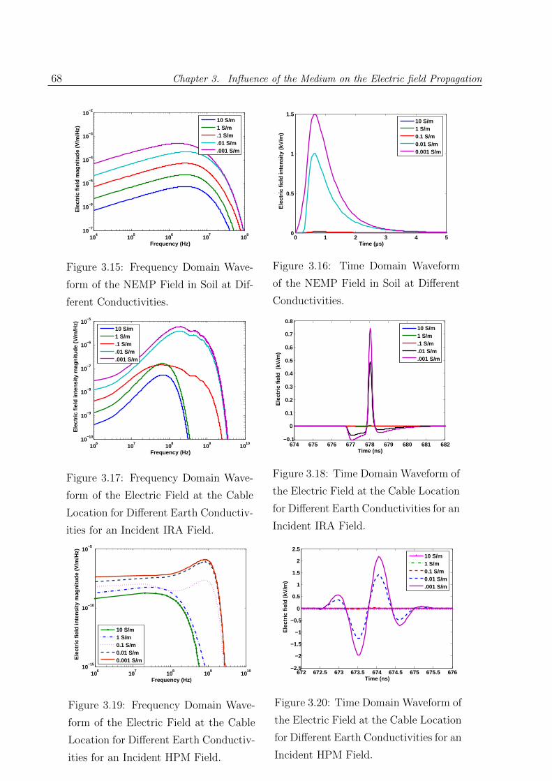
68 Chapter 3. Influence of the Medium on the Electric field Propagation
104
105
106
107
108
10−7
10−6
10−5
10−4
10−3
10−2
Frequency (Hz)
Ele
ctric
fiel
d m
agni
tude
(V
/m/H
z)
10 S/m1 S/m.1 S/m.01 S/m.001 S/m
Figure 3.15: Frequency Domain Wave-
form of the NEMP Field in Soil at Dif-
ferent Conductivities.
0 1 2 3 4 50
0.5
1
1.5
Time (µs)
Ele
ctric
fiel
d in
tens
ity (
kV/m
)
10 S/m1 S/m0.1 S/m0.01 S/m0.001 S/m
Figure 3.16: Time Domain Waveform
of the NEMP Field in Soil at Different
Conductivities.
106
107
108
109
1010
10−10
10−9
10−8
10−7
10−6
10−5
Frequency (Hz)
Ele
ctric
fiel
d in
tens
ity m
agni
tude
(V
/m/H
z) 10 S/m1 S/m.1 S/m.01 S/m.001 S/m
Figure 3.17: Frequency Domain Wave-
form of the Electric Field at the Cable
Location for Different Earth Conductiv-
ities for an Incident IRA Field.
674 675 676 677 678 679 680 681 682−0.1
0
0.1
0.2
0.3
0.4
0.5
0.6
0.7
0.8
Time (ns)
Ele
ctric
fiel
d (
kV/m
)
10 S/m1 S/m.1 S/m.01 S/m.001 S/m
Figure 3.18: Time Domain Waveform of
the Electric Field at the Cable Location
for Different Earth Conductivities for an
Incident IRA Field.
106
107
108
109
1010
10−15
10−10
10−5
Frequency (Hz)
Ele
ctric
fiel
d in
tens
ity m
agni
tude
(V
/m/H
z)
10 S/m1 S/m0.1 S/m0.01 S/m0.001 S/m
Figure 3.19: Frequency Domain Wave-
form of the Electric Field at the Cable
Location for Different Earth Conductiv-
ities for an Incident HPM Field.
672 672.5 673 673.5 674 674.5 675 675.5 676−2.5
−2
−1.5
−1
−0.5
0
0.5
1
1.5
2
2.5
Time (ns)
Ele
ctric
fiel
d (k
V/m
)
10 S/m1 S/m0.1 S/m0.01 S/m.001 S/m
Figure 3.20: Time Domain Waveform of
the Electric Field at the Cable Location
for Different Earth Conductivities for an
Incident HPM Field.
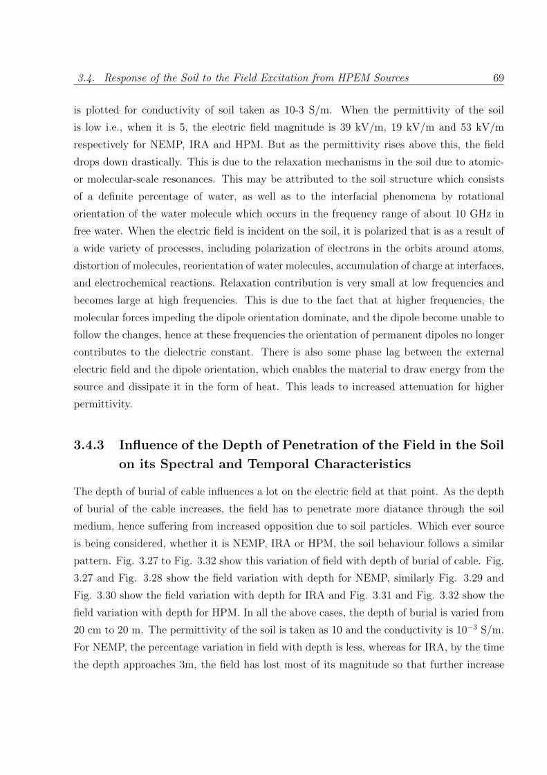
3.4. Response of the Soil to the Field Excitation from HPEM Sources 69
is plotted for conductivity of soil taken as 10-3 S/m. When the permittivity of the soil
is low i.e., when it is 5, the electric field magnitude is 39 kV/m, 19 kV/m and 53 kV/m
respectively for NEMP, IRA and HPM. But as the permittivity rises above this, the field
drops down drastically. This is due to the relaxation mechanisms in the soil due to atomic-
or molecular-scale resonances. This may be attributed to the soil structure which consists
of a definite percentage of water, as well as to the interfacial phenomena by rotational
orientation of the water molecule which occurs in the frequency range of about 10 GHz in
free water. When the electric field is incident on the soil, it is polarized that is as a result of
a wide variety of processes, including polarization of electrons in the orbits around atoms,
distortion of molecules, reorientation of water molecules, accumulation of charge at interfaces,
and electrochemical reactions. Relaxation contribution is very small at low frequencies and
becomes large at high frequencies. This is due to the fact that at higher frequencies, the
molecular forces impeding the dipole orientation dominate, and the dipole become unable to
follow the changes, hence at these frequencies the orientation of permanent dipoles no longer
contributes to the dielectric constant. There is also some phase lag between the external
electric field and the dipole orientation, which enables the material to draw energy from the
source and dissipate it in the form of heat. This leads to increased attenuation for higher
permittivity.
3.4.3 Influence of the Depth of Penetration of the Field in the Soil
on its Spectral and Temporal Characteristics
The depth of burial of cable influences a lot on the electric field at that point. As the depth
of burial of the cable increases, the field has to penetrate more diatance through the soil
medium, hence suffering from increased opposition due to soil particles. Which ever source
is being considered, whether it is NEMP, IRA or HPM, the soil behaviour follows a similar
pattern. Fig. 3.27 to Fig. 3.32 show this variation of field with depth of burial of cable. Fig.
3.27 and Fig. 3.28 show the field variation with depth for NEMP, similarly Fig. 3.29 and
Fig. 3.30 show the field variation with depth for IRA and Fig. 3.31 and Fig. 3.32 show the
field variation with depth for HPM. In all the above cases, the depth of burial is varied from
20 cm to 20 m. The permittivity of the soil is taken as 10 and the conductivity is 10−3 S/m.
For NEMP, the percentage variation in field with depth is less, whereas for IRA, by the time
the depth approaches 3m, the field has lost most of its magnitude so that further increase

70 Chapter 3. Influence of the Medium on the Electric field Propagation
104
105
106
107
108
10−6
10−5
10−4
10−3
Frequency (Hz)
Ele
ctric
fiel
d in
tens
ity m
agni
tude
(V
/m/H
z) 5101220
Figure 3.21: Frequency Domain Wave-
form of NEMP Field in Soil at Different
Permittivities.
0 1 2 3 4 50
5
10
15
20
25
30
35
40
Time (µs)
Ele
ctric
fiel
d in
tens
ity (
kV/m
)
5101220
Figure 3.22: Time Domain Waveform
of NEMP Field in Soil at Different
Permittivities.
106
107
108
109
1010
10−10
10−9
10−8
10−7
10−6
10−5
Frequency (Hz)
Ele
ctric
fiel
d in
tens
ity m
agni
tude
(V
/m/H
z)
5101220
Figure 3.23: Frequency Domain Wave-
form of the Electric Field at the Cable
Location at Different Earth Permittiv-
ity for an Incident IRA Field.
675 676 677 678 679 680
0
5
10
15
20
Time (ns)
Ele
ctri
c fi
eld
(kV
/m)
5101215
Figure 3.24: Time Domain Waveform of
the Electric Field at the Cable Location
at Different Earth Permittivity for an
Incident IRA Field.
106
107
108
109
1010
10−10
10−8
10−6
10−4
Frequency (Hz)
Ele
ctric
fiel
d in
tens
ity m
agni
tude
(V
/m/H
z)
5101520
Figure 3.25: Frequency Domain Wave-
form of the Electric Field at the Cable
Location at Different Earth Permittiv-
ity for an Incident HPM Field.
672 672.5 673 673.5 674 674.5 675 675.5 676−60
−40
−20
0
20
40
60
Time (ns)
Ele
ctric
fiel
d (k
V/m
)
5101520
Figure 3.26: Time Domain Waveform of
the Electric Field at the Cable Location
at Different Earth Permittivity for an
Incident HPM Field.

3.5. Case Study of Typical Types of Soils 71
in depth leads to a very feeble field having no significant magnitude. Also as the depth
increases, the IRA field pattern changes from its basic shape at low depths and is found
to have predominantly a centre frequency around 0.1 GHz. This prominence in the field at
that frequency is on account of the selective absorption by soil on some of the frequencies
present in the IRA field. In the case of HPM, the field magnitude is negligibly small, once
the depth increases above 2 m. Also the field doesn’t have any prominent centre frequency
at higher depths of penetration. The soil characteristics described in the previous sections
are actually a function of the percentage water content that varies steadily with increase in
the depth. This variation in the soil characteristics leads to the fields being attenuated more
and more as the depth increases.
3.5 Case Study of Typical Types of Soils
In the previous sections, we have seen the influence of soil conductivity, permittivity and
the depth of burial of the cable on the electric field characteristics from different HPEM
sourceshave been presented and discussed. In this section, a case study is conducted on
the different types of soils available and hence to see what will be the characteristics of the
fields from the different HPEM sources in these soil varieties. The soil samples taken are
pertaining to different regions.
(a) City industrial area soils ε∞=3, σ0 = 10−4
(b) Soils in mountainous regions ε∞=5, σ0 = 5×10⁻³
(c) Soils in the dry sandy area ε∞=10, σ0 = 4×10⁻³
(d) Rich agricultural lands with soils ε∞=15, σ0 = 10−2
(e) Pastoral hills with soils ε∞=20, σ0 = 4×10⁻²
(f) Highly moist ground soils ε∞=30, σ0 = 5×10⁻²
The electric field is plotted at a depth of 1 m from the earth’s surface, with the soils of
the above characteristics taken into consideration, so that the effect of variation of the soil
medium on the electric field can be analysed
The plot of the electric field intensity for an NEMP source is shown in Fig. 3.33 and
Fig. 3.34. The frequency domain plot of the electric field shows that the field pattern match
exactly at lower frequencies for all the different soil varieties. But as the frequency rises
above 1 MHz, there is a variation in the electric field plots between different soils, and this

72 Chapter 3. Influence of the Medium on the Electric field Propagation
104
105
106
107
108
10−6
10−5
10−4
10−3
10−2
10−1
Frequency (Hz)
Ele
ctric
fiel
d in
tens
ity m
agni
tude
(V
/m/H
z) 0.2 m0.5 m1 m1.5 m2 m3 m5 m10 m20 m
Figure 3.27: Frequency Domain Wave-
form of NEMP Field in Soil at Different
Depths.
0 1 2 3 4 50
0.5
1
1.5
2
2.5
3
3.5
Time (µs)
Ele
ctric
fiel
d (k
V/m
)
0.2 m0.5 m1 m1.5 m2 m3 m5 m10 m20 m
Figure 3.28: Time Domain Waveform of
NEMP Field in Soil at Different Depths.
106
107
108
109
1010
10−10
10−9
10−8
10−7
10−6
10−5
Frequency (Hz)
Ele
ctric
fiel
d in
tens
ity m
agni
tude
(V
/m/H
z)
0.2 m0.5 m1 m1.5 m2 m3 m5 m10 m20 m
Figure 3.29: Frequency Domain Wave-
form of the Electric Field at the Cable
Location at Different Depths of Burial
of the Cable.
700 750 800 850 900
0
0.2
0.4
0.6
0.8
1
1.2
1.4
1.6
Time (ns)
Ele
ctri
c fi
eld
(kV
/m)
0.2 m0.5 m1 m1.5 m2 m3 m5 m10 m20 m
Figure 3.30: Time Domain Waveform
of the Electric Field at the Cable Loca-
tion at Different Depths of Burial of the
Cable.
106
107
108
109
1010
10−12
10−10
10−8
10−6
Frequency (Hz)
Ele
ctric
fiel
d in
tens
ity m
agni
tude
(V
/m/H
z)
0.2 m0.5 m1 m2 m5 m
Figure 3.31: Frequency Domain Wave-
form of the Electric Field from an HPM
Source at the Cable Location at Differ-
ent Depths of Burial of the Cable.
680 700 720 740 760 780 800−5
0
5
Time (ns)
Ele
ctric
fiel
d (k
V/m
)
0.2 m0.5 m0.7 m1 m1.5 m2 m3 m5 m10 m
Figure 3.32: Time Domain Waveform
of the Electric Field from an HPM
Source at the Cable Location at Differ-
ent Depths of Burial of the Cable.
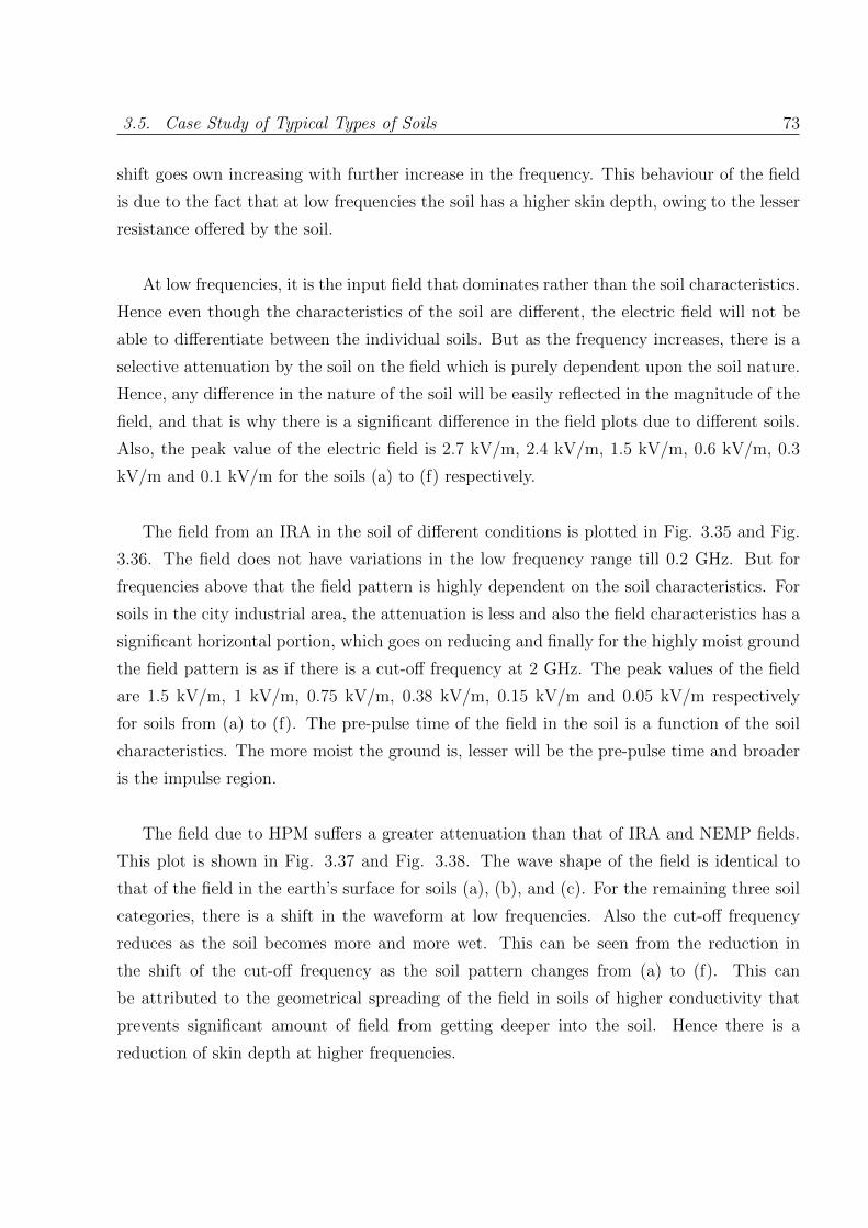
3.5. Case Study of Typical Types of Soils 73
shift goes own increasing with further increase in the frequency. This behaviour of the field
is due to the fact that at low frequencies the soil has a higher skin depth, owing to the lesser
resistance offered by the soil.
At low frequencies, it is the input field that dominates rather than the soil characteristics.
Hence even though the characteristics of the soil are different, the electric field will not be
able to differentiate between the individual soils. But as the frequency increases, there is a
selective attenuation by the soil on the field which is purely dependent upon the soil nature.
Hence, any difference in the nature of the soil will be easily reflected in the magnitude of the
field, and that is why there is a significant difference in the field plots due to different soils.
Also, the peak value of the electric field is 2.7 kV/m, 2.4 kV/m, 1.5 kV/m, 0.6 kV/m, 0.3
kV/m and 0.1 kV/m for the soils (a) to (f) respectively.
The field from an IRA in the soil of different conditions is plotted in Fig. 3.35 and Fig.
3.36. The field does not have variations in the low frequency range till 0.2 GHz. But for
frequencies above that the field pattern is highly dependent on the soil characteristics. For
soils in the city industrial area, the attenuation is less and also the field characteristics has a
significant horizontal portion, which goes on reducing and finally for the highly moist ground
the field pattern is as if there is a cut-off frequency at 2 GHz. The peak values of the field
are 1.5 kV/m, 1 kV/m, 0.75 kV/m, 0.38 kV/m, 0.15 kV/m and 0.05 kV/m respectively
for soils from (a) to (f). The pre-pulse time of the field in the soil is a function of the soil
characteristics. The more moist the ground is, lesser will be the pre-pulse time and broader
is the impulse region.
The field due to HPM suffers a greater attenuation than that of IRA and NEMP fields.
This plot is shown in Fig. 3.37 and Fig. 3.38. The wave shape of the field is identical to
that of the field in the earth’s surface for soils (a), (b), and (c). For the remaining three soil
categories, there is a shift in the waveform at low frequencies. Also the cut-off frequency
reduces as the soil becomes more and more wet. This can be seen from the reduction in
the shift of the cut-off frequency as the soil pattern changes from (a) to (f). This can
be attributed to the geometrical spreading of the field in soils of higher conductivity that
prevents significant amount of field from getting deeper into the soil. Hence there is a
reduction of skin depth at higher frequencies.
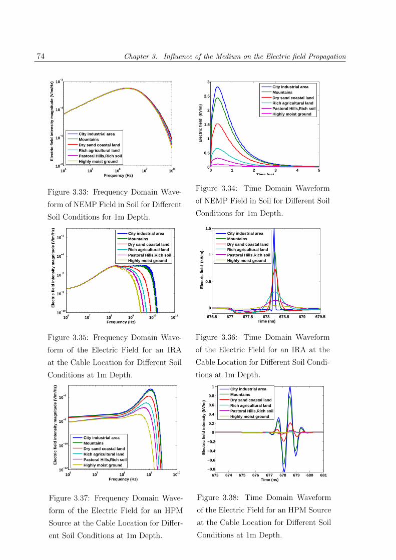
74 Chapter 3. Influence of the Medium on the Electric field Propagation
104
105
106
107
108
10−6
10−5
10−4
10−3
Frequency (Hz)
Ele
ctric
fiel
d in
tens
ity m
agni
tude
(V
/m/H
z)
City industrial areaMountainsDry sand coastal landRich agricultural landPastoral Hills,Rich soilHighly moist ground
Figure 3.33: Frequency Domain Wave-
form of NEMP Field in Soil for Different
Soil Conditions for 1m Depth.
0 1 2 3 4 50
0.5
1
1.5
2
2.5
3
Time (µs)
Ele
ctric
fiel
d (
kV/m
)
City industrial areaMountainsDry sand coastal landRich agricultural landPastoral Hills,Rich soilHighly moist ground
Figure 3.34: Time Domain Waveform
of NEMP Field in Soil for Different Soil
Conditions for 1m Depth.
106
107
108
109
1010
1011
10−10
10−8
10−6
10−4
10−2
Frequency (Hz)
Ele
ctric
fiel
d in
tens
ity m
agni
tude
(V
/m/H
z) City industrial areaMountainsDry sand coastal landRich agricultural landPastoral Hills,Rich soilHighly moist ground
Figure 3.35: Frequency Domain Wave-
form of the Electric Field for an IRA
at the Cable Location for Different Soil
Conditions at 1m Depth.
676.5 677 677.5 678 678.5 679 679.5
0
0.5
1
1.5
Time (ns)
Ele
ctri
c fi
eld
(kV
/m)
City industrial areaMountainsDry sand coastal landRich agricultural landPastoral Hills,Rich soilHighly moist ground
Figure 3.36: Time Domain Waveform
of the Electric Field for an IRA at the
Cable Location for Different Soil Condi-
tions at 1m Depth.
106
107
108
109
1010
10−12
10−10
10−8
10−6
Frequency (Hz)
Ele
ctric
fiel
d in
tens
ity m
agni
tude
(V
/m/H
z)
City industrial areaMountainsDry sand coastal landRich agricultural landPastoral Hills,Rich soilHighly moist ground
Figure 3.37: Frequency Domain Wave-
form of the Electric Field for an HPM
Source at the Cable Location for Differ-
ent Soil Conditions at 1m Depth.
673 674 675 676 677 678 679 680 681
−0.8
−0.6
−0.4
−0.2
0
0.2
0.4
0.6
0.8
1
Time (ns)
Ele
ctric
fiel
d in
tens
ity (
kV/m
)
City industrial areaMountainsDry sand coastal landRich agricultural landPastoral Hills,Rich soilHighly moist ground
Figure 3.38: Time Domain Waveform
of the Electric Field for an HPM Source
at the Cable Location for Different Soil
Conditions at 1m Depth.

3.6. Chapter Summary 75
3.6 Chapter Summary
The electric fields in the air and in the soil for different characteristic properties of these
media have been computed, by taking into account the reflection and transmission coefficients
from the soil. The following conclusions can be drawn from the results presented:
• The electric field propagation in any medium is influenced by the properties of the
medium, whether it is air or soil.
• As the height increases the magnitude of the electric field decreases for IRA and HPM
sources and also the time before which the field waveform starts is increased.)
• For low soil conductivities the attenuation constant of the soil saturates fast, but if the
conductivity increases the attenuation constant saturates at higher frequencies.
• For low soil conductivities, the conduction current to displacement current is low and
it increases at higher conductivity. However, the skin depth follows a reverse trend.
• A soil medium can be electromagnetically viewed as a four component dielectric mix-
ture consisting of soil particles, air voids, bound water, and free water.
• When electric field is incident on the soil, it is polarized that is as a result of a wide
variety of processes, including polarization of electrons in the orbits around atoms,
distortion of molecules, reorientation of water molecules, accumulation of charge at
interfaces, and electrochemical reactions.
• Whatever is the HPEM source, an increase in the soil conductivity results in more
attenuation of the field. Also there is a significant loss of high frequency components
in the GHz range in the field due to selective absorption by the soil. This effect cause
the percentage attenuation to be maximum for HPM and minimum for NEMP and
IRA lying in between these two extremities. This is because HPM is mainly a narrow
band source with high frequency components in the GHz range, IRA and NEMP are
wideband sources and has spectral content in the MHz range.
• Increase in permittivity of the soil causes more attenuation of the electric field for all
HPEM sources. This is due to the relaxation mechanisms in the soil due to atomic- or
molecular-scale resonances.

76 Chapter 3. Influence of the Medium on the Electric field Propagation
• As the depth of burial of the cable increases, the field has to penetrate more through
the soil medium, hence suffering from increased opposition due to soil particles. Hence
the field magnitude drops at higher depths.
• Soils in the city industrial areas have a higher field penetration and soils in the moist
wet lands provides the maximum attenuation.
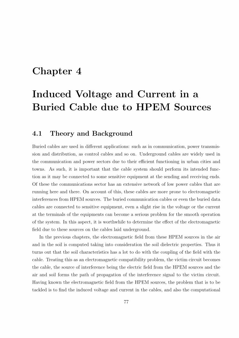
Chapter 4
Induced Voltage and Current in a
Buried Cable due to HPEM Sources
4.1 Theory and Background
Buried cables are used in different applications: such as in communication, power transmis-
sion and distribution, as control cables and so on. Underground cables are widely used in
the communication and power sectors due to their efficient functioning in urban cities and
towns. As such, it is important that the cable system should perform its intended func-
tion as it may be connected to some sensitive equipment at the sending and receiving ends.
Of these the communications sector has an extensive network of low power cables that are
running here and there. On account of this, these cables are more prone to electromagnetic
interferences from HPEM sources. The buried communication cables or even the buried data
cables are connected to sensitive equipment, even a slight rise in the voltage or the current
at the terminals of the equipments can become a serious problem for the smooth operation
of the system. In this aspect, it is worthwhile to determine the effect of the electromagnetic
field due to these sources on the cables laid underground.
In the previous chapters, the electromagnetic field from these HPEM sources in the air
and in the soil is computed taking into consideration the soil dielectric properties. Thus it
turns out that the soil characteristics has a lot to do with the coupling of the field with the
cable. Treating this as an electromagnetic compatibility problem, the victim circuit becomes
the cable, the source of interference being the electric field from the HPEM sources and the
air and soil forms the path of propagation of the interference signal to the victim circuit.
Having known the electromagnetic field from the HPEM sources, the problem that is to be
tackled is to find the induced voltage and current in the cables, and also the computational
77

78 Chapter 4. Induced Voltage and Current in a Buried Cable due to HPEM Sources
method adopted for the same.
4.2 Underground Cable Getting Illuminated by HPEM
Sources
The Fig. 4.1 gives the schematic of a cable getting illuminated by the electromagnetic fields
due to the different HPEM interference sources. The earth plane is considered to be of infinite
extent. The cable is buried such that the midpoint of the cable is aligned with the boresight
of the antennae in the case of IRA and HPM sources. In this work, only direct radiation
from IRA and HPM sources are considered. The NEMP field is present uniformly in the
region surrounding the cable so that the cable has a homogeneous illumination throughout
its length due to NEMP field. The IRA and HPM sources are located at a distance of 100
m above the earth’s surface. Different types of soils are considered in the last chapter and
also some case studies are also presented. For the present work, to find the coupling with
the cable, it is assumed that the cable runs in a dry sandy land. This type of soil has
characteristic properties that will lead to an induced voltage which is neither too low nor
too high. The conductivity of this soil is 0.001 S/m and the relative dielectric constant is
10.
4.3 Coupling with the Cable
HPEM electric field coupling with the cable is done in two stages [93]-[98]:
• Coupling to the external circuit, and
• Coupling to the internal circuit
The detailed circuit configuration of the two circuits is given in Fig. 4.2. The equivalent
circuit representation is shown in Fig. 4.3. The external circuit consists of the soil whose
impedance is Zsoil and admittance is Yg [95], the outer layer of the cable shield whose
impedance is Zsh and the outer dielectric layer which has a series impedance of Zins and a
capacitance of Xc. The internal circuit consists of the inner layer of the shield of impedance
Zss., inner insulation of impedance Zind and admittance of Yins as well as conductor of
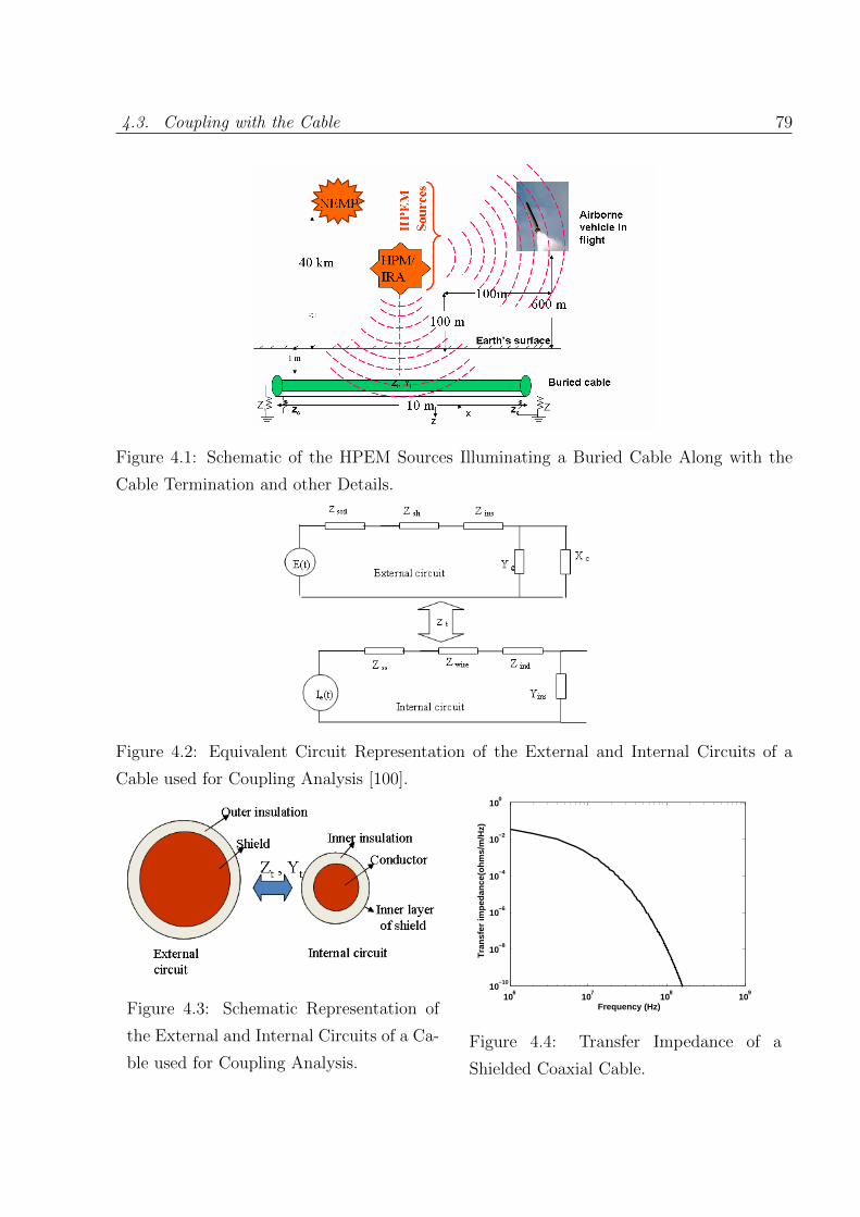
4.3. Coupling with the Cable 79
Figure 4.1: Schematic of the HPEM Sources Illuminating a Buried Cable Along with the
Cable Termination and other Details.
Figure 4.2: Equivalent Circuit Representation of the External and Internal Circuits of a
Cable used for Coupling Analysis [100].
Figure 4.3: Schematic Representation of
the External and Internal Circuits of a Ca-
ble used for Coupling Analysis.
106
107
108
109
10−10
10−8
10−6
10−4
10−2
100
Frequency (Hz)
Tra
nsfe
r im
peda
nce(
ohm
s/m
/Hz)
Figure 4.4: Transfer Impedance of a
Shielded Coaxial Cable.

80 Chapter 4. Induced Voltage and Current in a Buried Cable due to HPEM Sources
impedance Zwire. The two circuits are coupled by means of the shield transfer impedance,
Zt.
The value of Zt is computed using Schelkunoffs equation [95]. According to this equation
transfer impedance can be written as :
ZT =1
2πaσT
(1 + j)Tδ
sinh(1 + j)Tδ
(4.1)
The transfer impedance for the shielded cable that is used for the present work is shown
in Fig. 4.4. The transfer impedance is a function of the type of the cable, the frequencies of
the field that is going to excite the cable and also that of the shield thickness. This varies
with the frequency and is tens of milli-ohms per meter at low frequency. It also drops with
frequency. The incident electric field reaching the cable will induce voltage in the shield.
This can be determined by assuming the shield as a single core conductor with an outer
layer of insulation. At all the points along the length of the shield, there is an excitation due
to the field. This is a case of the distributed excitation and hence the current is induced at
every point on the cable at the same time.
The terminal characteristics of the cable matters has to be considered in the induced
voltage computation, because the net voltage or current on the cable is influenced by the
type of cable termination used. This can be attributed to the concept of travelling waves,
as the net voltage/current at any point is the sum of the travelling wave components of
the voltages / currents coming from either sides of the observation point. These travelling
wave components have a transmitted part and a reflected part, the reflected wave being a
function of the terminal impedance of the cable. Hence the nature of the termination is
critical in the evaluation of the induced parameters. In the present case, both the shield
and the inner conductor are terminated respectively by their own characteristic impedances
as shown in the Fig. 4.1. In this case, there are no reflections of the shield current from
the ends and likewise there is no reflection of the current in the inner conductor from the
ends of the cable. These currents propagate to either ends of the cable and get terminated
because of the matching impedances connected at the end points. The method of analysis
should accommodate for these effects. Several methods are used in practice to find the
coupling. Most of them are based on the transmission line model of the cable [95]. Since
the frequency encountered in the HPEM sources coupling varies from MHz to GHz range,
the method used for coupling should accommodate for these huge frequencies involved. At
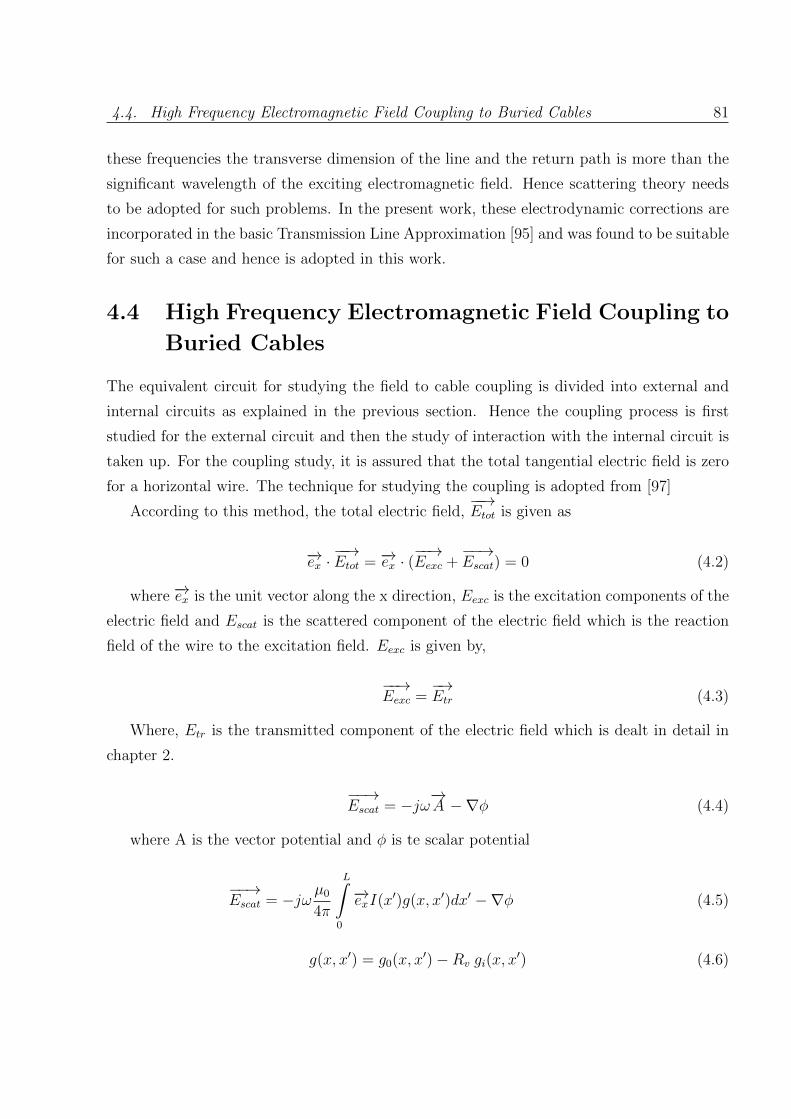
4.4. High Frequency Electromagnetic Field Coupling to Buried Cables 81
these frequencies the transverse dimension of the line and the return path is more than the
significant wavelength of the exciting electromagnetic field. Hence scattering theory needs
to be adopted for such problems. In the present work, these electrodynamic corrections are
incorporated in the basic Transmission Line Approximation [95] and was found to be suitable
for such a case and hence is adopted in this work.
4.4 High Frequency Electromagnetic Field Coupling to
Buried Cables
The equivalent circuit for studying the field to cable coupling is divided into external and
internal circuits as explained in the previous section. Hence the coupling process is first
studied for the external circuit and then the study of interaction with the internal circuit is
taken up. For the coupling study, it is assured that the total tangential electric field is zero
for a horizontal wire. The technique for studying the coupling is adopted from [97]
According to this method, the total electric field,−−→Etot is given as
−→ex ·−−→Etot = −→ex · (
−−→Eexc +
−−→Escat) = 0 (4.2)
where −→ex is the unit vector along the x direction, Eexc is the excitation components of the
electric field and Escat is the scattered component of the electric field which is the reaction
field of the wire to the excitation field. Eexc is given by,
−−→Eexc =
−→Etr (4.3)
Where, Etr is the transmitted component of the electric field which is dealt in detail in
chapter 2.
−−→Escat = −jω
−→A −∇φ (4.4)
where A is the vector potential and φ is te scalar potential
−−→Escat = −jω µ0
4π
L∫0
−→exI(x′)g(x, x′)dx′ −∇φ (4.5)
g(x, x′) = g0(x, x′)−Rv gi(x, x
′) (4.6)
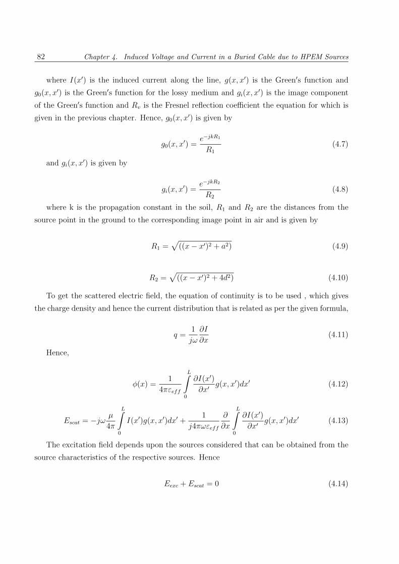
82 Chapter 4. Induced Voltage and Current in a Buried Cable due to HPEM Sources
where I(x′) is the induced current along the line, g(x, x′) is the Green′s function and
g0(x, x′) is the Green′s function for the lossy medium and gi(x, x
′) is the image component
of the Green′s function and Rv is the Fresnel reflection coefficient the equation for which is
given in the previous chapter. Hence, g0(x, x′) is given by
g0(x, x′) =
e−jkR1
R1
(4.7)
and gi(x, x′) is given by
gi(x, x′) =
e−jkR2
R2
(4.8)
where k is the propagation constant in the soil, R1 and R2 are the distances from the
source point in the ground to the corresponding image point in air and is given by
R1 =√
((x− x′)2 + a2) (4.9)
R2 =√
((x− x′)2 + 4d2) (4.10)
To get the scattered electric field, the equation of continuity is to be used , which gives
the charge density and hence the current distribution that is related as per the given formula,
q =1
jω
∂I
∂x(4.11)
Hence,
φ(x) =1
4πεeff
L∫0
∂I(x′)
∂x′g(x, x′)dx′ (4.12)
Escat = −jω µ
4π
L∫0
I(x′)g(x, x′)dx′ +1
j4πωεeff
∂
∂x
L∫0
∂I(x′)
∂x′g(x, x′)dx′ (4.13)
The excitation field depends upon the sources considered that can be obtained from the
source characteristics of the respective sources. Hence
Eexc + Escat = 0 (4.14)

4.4. High Frequency Electromagnetic Field Coupling to Buried Cables 83
Solving the above equation gives the induced current at any point on the wire. According
to the standard TL theory, the scattered voltage is,
Vs(x) = −ds∫0
Ez(z, x)dz (4.15)
where Ez(z, x) is the vertical electric field at the given depth
Vs(x) = φ(d, x)− φ(0, x) (4.16)
But
φ(0, x) = 0 (4.17)
Or,
dVs(x)
dx+ jω
µ0
4π
L∫0
I(x′)g(x, x′)dx′ = Eexc(d, x) (4.18)
d
dx
L∫0
I(x′)g(x, x′)dx′ + jω4πε0Vs(x) = 0 (4.19)
Solving the above equations for the external circuit, we can get the current and voltage
induced at all the desired locations on the cable. For example, the net current at any point
is the sum of all the currents reaching that point. If there are n+1 points on the cable, then
I(x = p) = −p−1∑x=0
I(x) + I(x = p) +x=n∑x=p+1
(4.20)
These n+1 points are shown in Fig. 4.5. along with the direction of the travelling waves
of voltages and currents. In the above equation the first term refers to the current flowing
from the left hand side of the desired point and the last term refers to the net current
flowing from the right hand side. The middle term is the contribution to the current due to
the induced current at the point of interest itself. So depending upon where the observation
point is located, the relative contribution from either side of the observation point varies.
This causes variation in the characteristics of the current at that point. A similar explanation
holds good for the induced voltage also.

84 Chapter 4. Induced Voltage and Current in a Buried Cable due to HPEM Sources
The current induced in the shield gets coupled to the inner circuit. Only a small portion
of this shield current gets coupled to the inner circuit, which is given as Zt ∗ I(x), where
Zt is the transfer impedance of the cable. This voltage term forms the excitation term to
a similar set of transmission line equations as in equation 4.18 and equation 4.19. Solving
these equations will give the induced current and voltages on the inner conductor of the
cable.
4.5 Validation of the Proposed Method
The method used for computing the induced voltage/current is validated by taking one of the
HPEM sources and computing the induced current in a wire buried at a depth of 1 m in soil.
HPM is taken as the excitation source and the current is computed at the midpoint of the
wire with HPM antenna at a distance of 1 km from the earth’s surface. The induced current
so obtained is plotted in Fig. 4.6 and Fig. 4.7. The current obtained by the proposed method
is validated by computing the induced current using the full wave model incorporating the
Sommerfeld Integral using the commercially available NEC software. The data used for
validation are as follows:
• SIMULATION PLATFORM : NEC V-4
• Number of segments: 801
• Frequency points: 1 MHz-2300 MHz step: 1 MHz
• Lossy ground model: Sommerfeld Integral
• Time domain solution: IFFT transformation
The result shows close similarity to the induced current computation using the Enhanced
Transmission Line Model (ETLM). All the transition points match closely at the respective
frequencies in both the figures. And the shape is maintained too, except for an additional
jump in the waveform occurring at 3.4 GHz, in the falling portion of the waveform for the
induced current. Because of the close matching, this method (ETLM) is used for computing
the induced current/ voltage in the cable in this work.
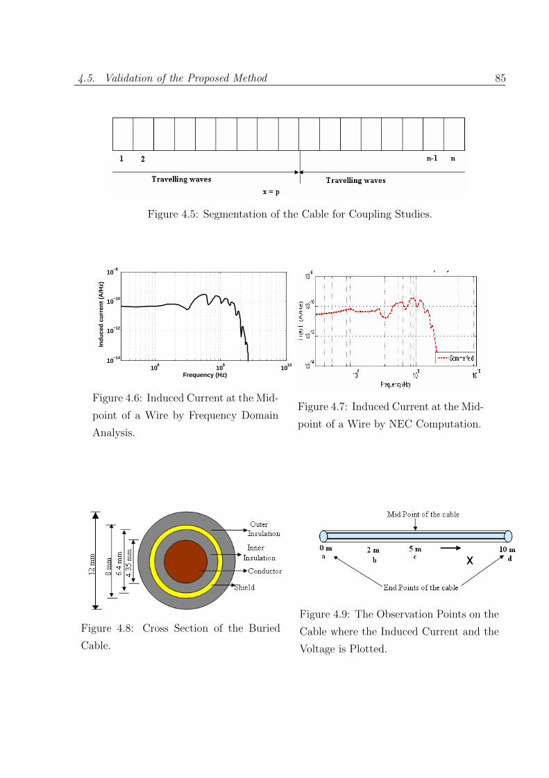
4.5. Validation of the Proposed Method 85
Figure 4.5: Segmentation of the Cable for Coupling Studies.
108
109
1010
10−14
10−12
10−10
10−8
Frequency (Hz)
Indu
ced
curr
ent (
A/H
z)
Figure 4.6: Induced Current at the Mid-
point of a Wire by Frequency Domain
Analysis.
Figure 4.7: Induced Current at the Mid-
point of a Wire by NEC Computation.
Figure 4.8: Cross Section of the Buried
Cable.
Figure 4.9: The Observation Points on the
Cable where the Induced Current and the
Voltage is Plotted.

86 Chapter 4. Induced Voltage and Current in a Buried Cable due to HPEM Sources
4.6 Induced Voltage/ Current in the Shield of the Ca-
ble due to the HPEM Sources
The method of induced current computation is explained in one of the previous section 4.2
to 4.4. Also the method so used is validated against a full wave current model and the results
using both the methods matched well. Using this method, the induced voltage and current
on a buried shielded cable is computed for the three HPEM sources, NEMP, IRA and HPM.
The cable is a shielded cable, the shielding of which is done by using tape wound galvanized
steel with negligible spacing between the turns. The cable is buried at a depth of 1m below
the earth’s surface. The length of the cable is taken as 10 m. The outer insulation and the
inner insulation used is PVC. The inner conductor is made of copper. The dimensions of
the cable is shown in Fig. 4.8. The cable is buried in a dry sandy soil having a permittivity
of 10 and conductivity of 10−3 S/m.
The electric field from the HPEM sources will travel initially through the air and then
get into the soil media where the field behaves in an entirely different fashion rather than in
the air. This behavioural mechanism is already given in chapter 3.
The response of the cable to the electric field from these sources is decided by how much
voltage and current is induced in it when the electric field due to these sources strike the
cable. The induced current and voltage is plotted at four points along the cable length.
These observation points are shown in the Fig. 4.9.In all the induced current and voltage
plots the labels a and d show the end points of the cable, b shows the observation point ant
a distance of 2m from the point a, and c shows the midpoint of the cable.These observation
points are marked in Fig. 4.9
4.6.1 Response of the Cable to NEMP Field
The induced current in the shield due to the electric field from an NEMP is shown in Fig.
4.10 to Fig. 4.18. The spectral characteristics of the induced current show a peak in the value
of the current at a frequency close to 1 MHz and the drop in current after this frequency
is more than the other side, where current slowly increases with rise in the frequency. This
drop in the current is attributed to the higher attenuation constant of the soil once the
frequency increases. The induced current has a peak value of 65 A at the midpoint of the
cable. There is a gradual reduction in the magnitude of the current from the midpoint of

4.6. Induced Voltage/ Current in the Shield of the Cable due to the HPEM Sources 87
the cable to the endpoints. The induced voltage in the shield is zero at the midpoint and
gradually rises to the ends. Also, the polarity of the voltage is different on either side of the
midpoint with a peak voltage of 4.8 kV at the endpoint of the cable. The current and the
voltage in the shield start after a delay time,
td = 1 / propagation velocity in soil = 10 ns
In both the current and voltage waveforms, the basic wave shape of the NEMP field,
i.e., the double exponential nature is preserved. In the inner conductor, the current has a
peak value of 1 A and the voltage has a peak magnitude of 80 V. The current in the inner
conductor starts after a delay time of 10 µs.
4.6.2 Response of the Cable to an IRA Field
The induced current and voltage in a shielded cable due to an IRA generated field can be
computed in the following manner. The IRA source is considered to be located at a distance
of 100 m from the earth’s surface. The field at the cable location is identified using the source
characteristics. For this the IRA source is so located that the boresight of the antenna strikes
exactly at the midpoint of the cable. This configuration gives a maximum field at the centre
of the cable. Now the field at all the points of the cable is taken as the source for computing
the induced parameters in the cable, by taking due consideration of the cable parameters.
The current thus computed in the cable shield is plotted in Fig. 4.19 to Fig. 4.20.
These figures show that the induced current in the cable shield is maximum at the centre
of the cable, where the electric field is the maximum. This peak magnitude of the current
is 150 A. The wave shape of the current has a prepulse followed by an impulse as expected
for an IRA type field. But once the observation point shifts from the centre of the cable
to the sides, i.e., to left or to the right of the centre, the current magnitude drops almost
exponentially with the distance, so that the magnitude of the current is 100 A and 75 A
respectively at observation points 2 m and 0 m, which corresponds to a distance of 3 m and
5m from the centre of the cable to the ends of the cable. The similar pattern is repeated
at both the sides from the centre, as the cable is symmetrical with respect to the field and
also there are no reflections from the endpoints. Fig. 4.20 shows a mesh plot of the current
along the cable, which shows the variation of the current along the cable. The current at
the midpoint of the cable starts after a delay time which is given by,
td = (100 m / velocity of propagation of the field in air) + (1/ velocity in soil) =

88 Chapter 4. Induced Voltage and Current in a Buried Cable due to HPEM Sources
104
105
106
107
108
10−7
10−6
10−5
10−4
Frequency (Hz)
Indu
ced
curr
ent
(A/H
z)
Figure 4.10: Frequency Domain Wave-
form of the Induced Current on the
Shield due to NEMP.
0 2 40
10203040506070
Time (µs)
Indu
ced
curr
ent (
A)
0 2 40
10203040506070
Time (µs)
Indu
ced
curr
ent (
A)
0 2 40
10203040506070
Time (µs)
Indu
ced
curr
ent (
A)
0 2 40
10203040506070
Time (µs)
Indu
ced
curr
ent (
A)
a b
c d
Figure 4.11: Time Domain Waveform of
the of Induced Current in the Shield.
0
5
10 05
10
0
20
40
60
80
100
Time (µs)Distance along the
length of the cable (m)
Indu
ced
curr
ent
(A)
10
20
30
40
50
60
70
80
Figure 4.12: Mesh Plot of the Induced
Current on the Shield.
0 2 4
−4
−2
0
Time (µs)
Indu
ced
volta
ge (
kV)
0 2 4
−4
−2
0
Time (µs)
Indu
ced
volta
ge (
kV)
0 2 4−1
−0.5
0
0.5
1
Time (µs)
Indu
ced
volta
ge (
kV)
0 2 40
1
2
3
4
5
Time (µs)
Indu
ced
volta
ge (
kV)
a b
c d
Figure 4.13: Time Domain Waveform of
the Induced Voltage on the Shield.
05
10 02
46−10
−5
0
5
10
Time (µs)Distance along the
length of the cable (m)
Indu
ced
volta
ge (
kV)
−6
−4
−2
0
2
4
6
Figure 4.14: Mesh Plot of the Induced
Voltage on the Shield.
0 50 100 150−1
−0.5
0
0.5
Time (µs)
Indu
ced
curr
ent (
A)
0 50 100 150−1
−0.5
0
0.5
Time (µs)
Indu
ced
curr
ent (
A)
0 50 100 150−1
−0.5
0
0.5
Time (µs)
Indu
ced
curr
ent (
A)
0 50 100 150−1
−0.5
0
0.5
Time (µs)
Indu
ced
curr
ent (
A)
a
c
b
d
Figure 4.15: Time Domain Waveform
of the Induced Current on the Inner
Conductor.
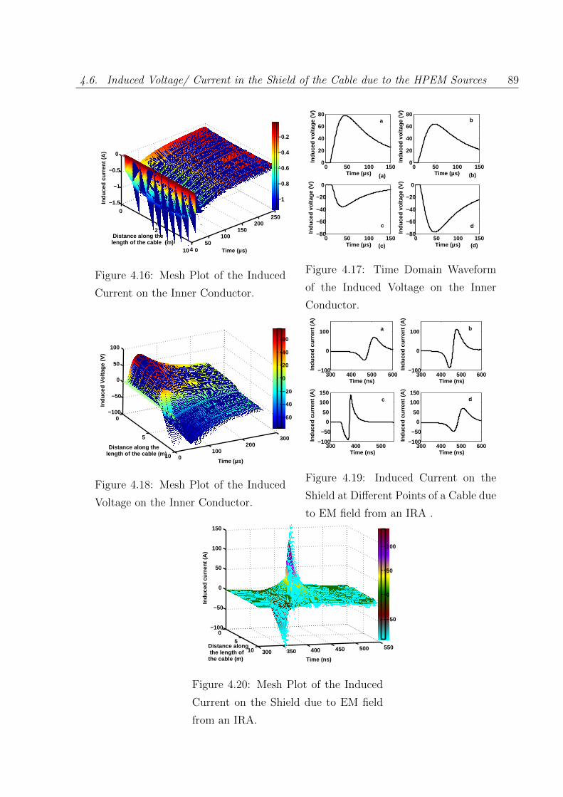
4.6. Induced Voltage/ Current in the Shield of the Cable due to the HPEM Sources 89
0
2
4 50
100150
200250
−1.5
−1
−0.5
0
Time (µs)
Distance along the length of the cable (m)
Indu
ced
curr
ent (
A)
−1
−0.8
−0.6
−0.4
−0.2
10 0
Figure 4.16: Mesh Plot of the Induced
Current on the Inner Conductor.
0 50 100 1500
20
40
60
80
Time (µs)
Indu
ced
volta
ge (
V)
0 50 100 1500
20
40
60
80
Time (µs)
Indu
ced
volta
ge (
V)
0 50 100 150−80
−60
−40
−20
0
Time (µs)
Indu
ced
volta
ge (
V)
0 50 100 150−80
−60
−40
−20
0
Time (µs)
Indu
ced
volta
ge (
V)
(a) (b)
(c) (d)
a
c
b
d
Figure 4.17: Time Domain Waveform
of the Induced Voltage on the Inner
Conductor.
0
5
10 0100
200300
−100
−50
0
50
100
Time (µs)
Distance along the length of the cable (m)
Indu
ced
Vol
tage
(V
)
−60
−40
−20
0
20
40
60
Figure 4.18: Mesh Plot of the Induced
Voltage on the Inner Conductor.
300 400 500 600−100
0
100
Time (ns)
Indu
ced
curr
ent (
A)
300 400 500 600−100
0
100
Time (ns)
Indu
ced
curr
ent (
A)
300 400 500−100
−50
0
50
100
150
Time (ns)
Indu
ced
curr
ent (
A)
300 400 500 600−100
−50
0
50
100
150
Time (ns)
Indu
ced
curr
ent (
A)
a b
c d
Figure 4.19: Induced Current on the
Shield at Different Points of a Cable due
to EM field from an IRA .
0
5
10 300 350 400 450 500 550
−100
−50
0
50
100
150
Time (ns)
Distance along the length of the cable (m)
Indu
ced
curr
ent (
A)
−50
0
50
100
Figure 4.20: Mesh Plot of the Induced
Current on the Shield due to EM field
from an IRA.
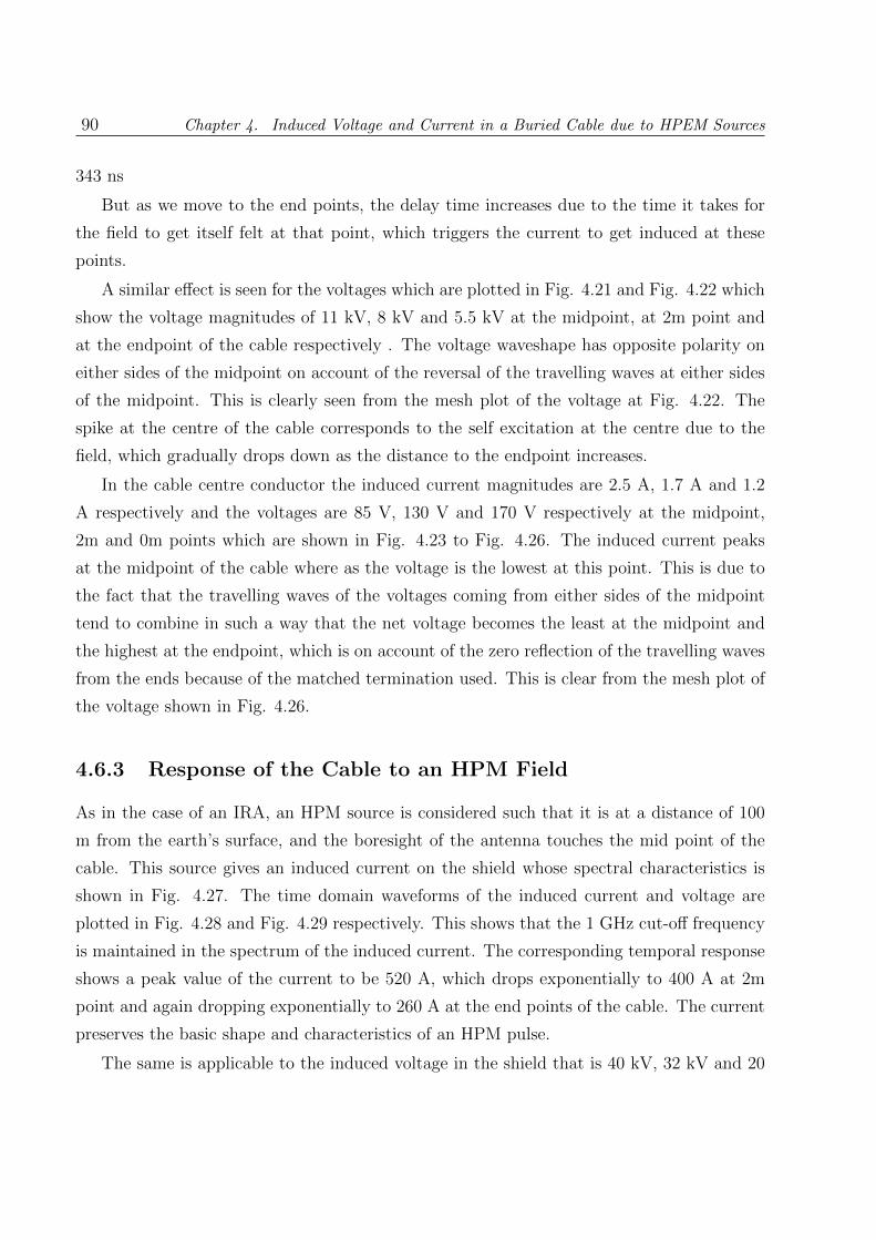
90 Chapter 4. Induced Voltage and Current in a Buried Cable due to HPEM Sources
343 ns
But as we move to the end points, the delay time increases due to the time it takes for
the field to get itself felt at that point, which triggers the current to get induced at these
points.
A similar effect is seen for the voltages which are plotted in Fig. 4.21 and Fig. 4.22 which
show the voltage magnitudes of 11 kV, 8 kV and 5.5 kV at the midpoint, at 2m point and
at the endpoint of the cable respectively . The voltage waveshape has opposite polarity on
either sides of the midpoint on account of the reversal of the travelling waves at either sides
of the midpoint. This is clearly seen from the mesh plot of the voltage at Fig. 4.22. The
spike at the centre of the cable corresponds to the self excitation at the centre due to the
field, which gradually drops down as the distance to the endpoint increases.
In the cable centre conductor the induced current magnitudes are 2.5 A, 1.7 A and 1.2
A respectively and the voltages are 85 V, 130 V and 170 V respectively at the midpoint,
2m and 0m points which are shown in Fig. 4.23 to Fig. 4.26. The induced current peaks
at the midpoint of the cable where as the voltage is the lowest at this point. This is due to
the fact that the travelling waves of the voltages coming from either sides of the midpoint
tend to combine in such a way that the net voltage becomes the least at the midpoint and
the highest at the endpoint, which is on account of the zero reflection of the travelling waves
from the ends because of the matched termination used. This is clear from the mesh plot of
the voltage shown in Fig. 4.26.
4.6.3 Response of the Cable to an HPM Field
As in the case of an IRA, an HPM source is considered such that it is at a distance of 100
m from the earth’s surface, and the boresight of the antenna touches the mid point of the
cable. This source gives an induced current on the shield whose spectral characteristics is
shown in Fig. 4.27. The time domain waveforms of the induced current and voltage are
plotted in Fig. 4.28 and Fig. 4.29 respectively. This shows that the 1 GHz cut-off frequency
is maintained in the spectrum of the induced current. The corresponding temporal response
shows a peak value of the current to be 520 A, which drops exponentially to 400 A at 2m
point and again dropping exponentially to 260 A at the end points of the cable. The current
preserves the basic shape and characteristics of an HPM pulse.
The same is applicable to the induced voltage in the shield that is 40 kV, 32 kV and 20
4.6. Induced Voltage/ Current in the Shield of the Cable due to the HPEM Sources 91
300 400 500 600 700−10
0
10
Time (ns)
Indu
ced
volta
ge (
kV)
300 400 500 600 700−10
0
10
Time (ns)
Indu
ced
volta
ge (
kV)
300 400 500 600 700−10
−5
0
5
10
Time (ns)
Indu
ced
volta
ge (
kV)
300 400 500 600 700−10
−5
0
5
10
Time (ns)
Indu
ced
volta
ge (
kV)
a
c d
b
Figure 4.21: Induced Voltage on the
Shield at Different Points of the Cable
due to EM field from an IRA.
0
5
10 300 350 400 450 500 550
−10
−5
0
5
10
15
Time (ns)
Indu
ced
volta
ge(k
V)
Distance along the length of the cable (m)
−5
0
5
10
Figure 4.22: Mesh Plot of the Induced
Voltage on the Shield due to the EM
field from an IRA.
200 400 600 800 10001200
−2
−1
0
1
Time (ns)
Indu
ced
curr
ent (
A)
200 400 600 800 10001200
−2
−1
0
1
Time (ns)
Indu
ced
curr
ent (
A)
200 400 600 800 10001200
−2
−1
0
1
Time (ns)
Indu
ced
curr
ent (
A)
200 400 600 800 10001200
−2
−1
0
1
Time (ns)
Indu
ced
curr
ent (
A)
a
dc
b
Figure 4.23: Induced Current on the In-
ner Conductor at Different Points of the
Cable due to the EM field from an IRA.
Figure 4.24: Mesh Plot of the Induced
Current on the Inner Conductor due to
the EM field from an IRA.
200 400 600 800 10001200−170
−100
−50
0
50
Time (ns)
Indu
ced
volta
ge (
V)
200 400 600 80010001200−170
−100
−50
0
50
Time (ns)
Indu
ced
volta
ge (
V)
200 400 600 800 10001200−50
0
50
100
170
Time (ns)
Indu
ced
volta
ge (
V)
200 400 600 800 10001200−50
0
50
100
170
Time (ns)
Indu
ced
volta
ge (
V)
a b
c d
Figure 4.25: Induced Voltage on the In-
ner Conductor at Different Points of the
Cable due to the EM field from an IRA.
Figure 4.26: Mesh Plot of the Induced
Voltage on the Inner Conductor due to
the EM field from an IRA.

92 Chapter 4. Induced Voltage and Current in a Buried Cable due to HPEM Sources
kV respectively at the endpoint of the cable, at 2 m and at the midpoint of the cable. The
polarity reversal between the induced voltages in either sides of the midpoint of the cable
is also clear from the Fig. 4.29. The time delay incurred before the current is felt at the
midpoint of the cable is 334 ns as in the case of IRA.
The induced current and voltage in the inner conductor of the cable are plotted in Fig.
4.30 to Fig. 4.32. In the inner conductor of the cable, the induced current characteristics
is such that the current drops very fast and almost by 100 MHz, the current is reduced sig-
nificantly. The high frequency components have vanished from the waveform of the induced
current waveform on the inner conductor that were present in the current induced on the
shield. This can be attributed due to the transfer impedance of the cable which is negligibly
small at frequencies close to GHz range. This can also be seen from the Fig. 4.30. The
induced current occurring on the inner conductor is 8 A, 6 A and 4 A at the midpoint, at
2 m and at the ends of the cable respectively. Also the induced voltage in the conductor is
600 V, 400 V and 300 V at the ends, at 2m and at the midpoint of the cable respectively.
4.7 Induced Current in Twisted Pair Cable due to HPEM
Sources
The present day communication cables are mostly twisted pair cables, because of the ad-
vantage of lower attenuation of the signals transmitted through these cables [98] as well
as their excellant performance in low to medium speed data transmission applications. The
twisted-pair cable is used extensively because of its low-loss, low-cost, and low-coupling char-
acteristics. At low frequencies, the coupling among cables is generally related to the magnetic
field that is produced in proximity to driven cables. A twisted-pair transmission line is a pair
of wires with circular cross-section, coated uniformly with a dielectric, and twisted about
each other with a uniform pitch. The wires are typically copper, and the dielectric is gen-
erally one of many plastics, depending upon the application. Multiple twisted-pairs can be
grouped together and encased in an insulating jacket, and twisted-pair transmission lines
can be either shielded or unshielded. There are thin, flexible cables that are easy to string
between walls. These cables can have more lines running through the same wiring ducts
and hence costs less per meter than any other type of LAN cable, electrical noise going into
or coming from the cable can be prevented and cross-talk is minimized. But at the same
time twisted pair’s are susceptible to electromagnetic interference that greatly depends on
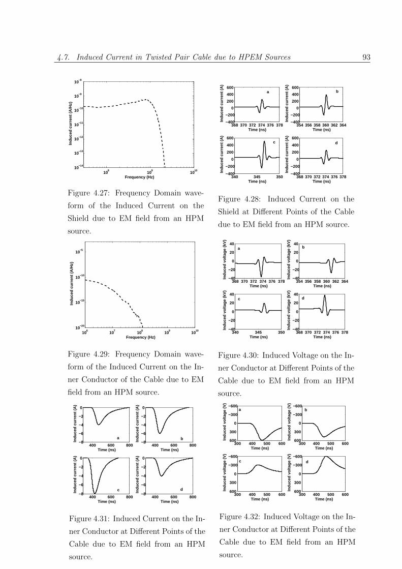
4.7. Induced Current in Twisted Pair Cable due to HPEM Sources 93
108
109
1010
10−14
10−13
10−12
10−11
10−10
10−9
10−8
Frequency (Hz)
Indu
ced
curr
ent (
A/H
z)
Figure 4.27: Frequency Domain wave-
form of the Induced Current on the
Shield due to EM field from an HPM
source.
368 370 372 374 376 378−400
−200
0
200
400
600
Time (ns)
Indu
ced
curr
ent (
A)
354 356 358 360 362 364−400
−200
0
200
400
600
Time (ns)
Indu
ced
curr
ent (
A)
340 345 350−400
−200
0
200
400
600
Time (ns)
Indu
ced
curr
ent (
A)
368 370 372 374 376 378−400
−200
0
200
400
600
Time (ns)
Indu
ced
curr
ent (
A)
c
a b
d
Figure 4.28: Induced Current on the
Shield at Different Points of the Cable
due to EM field from an HPM source.
106
107
108
109
1010
10−20
10−15
10−10
10−5
Frequency (Hz)
Indu
ced
curr
ent (
A/H
z)
Figure 4.29: Frequency Domain wave-
form of the Induced Current on the In-
ner Conductor of the Cable due to EM
field from an HPM source.
368 370 372 374 376 378−40
−20
0
20
40
Time (ns)
Indu
ced
volta
ge (
kV)
354 356 358 360 362 364−40
−20
0
20
40
Time (ns)In
duce
d vo
ltage
(kV
)
340 345 350−40
−20
0
20
40
Time (ns)
Indu
ced
volta
ge (
kV)
368 370 372 374 376 378−40
−20
0
20
40
Time (ns)
Indu
ced
volta
ge (
kV)
a
dc
b
Figure 4.30: Induced Voltage on the In-
ner Conductor at Different Points of the
Cable due to EM field from an HPM
source.
400 600 800−8
−6
−4
−2
0
Time (ns)
Indu
ced
curr
ent (
A)
400 600 800−8
−6
−4
−2
0
Time (ns)
Indu
ced
curr
ent (
A)
400 600 800−8
−6
−4
−2
0
Time (ns)
Indu
ced
curr
ent (
A)
400 600 800−8
−6
−4
−2
0
Time (ns)
Indu
ced
curr
ent (
A)
a b
c d
Figure 4.31: Induced Current on the In-
ner Conductor at Different Points of the
Cable due to EM field from an HPM
source.
300 400 500 600
−600
−300
0
300
600
Time (ns)
Indu
ced
volta
ge (
V)
300 400 500 600
−600
−300
0
300
600
Time (ns)
Indu
ced
volta
ge (
V)
300 400 500 600
−600
−300
0
300
600
Time (ns)
Indu
ced
volta
ge (
V)
300 400 500 600
−600
−300
0
300
600
Time (ns)
Indu
ced
volta
ge (
V)
a
c
b
d
Figure 4.32: Induced Voltage on the In-
ner Conductor at Different Points of the
Cable due to EM field from an HPM
source.
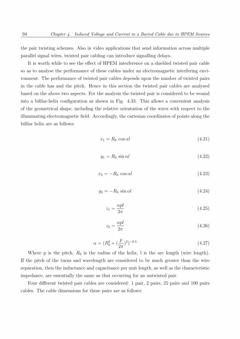
94 Chapter 4. Induced Voltage and Current in a Buried Cable due to HPEM Sources
the pair twisting schemes. Also in video applications that send information across multiple
parallel signal wires, twisted pair cabling can introduce signalling delays.
It is worth while to see the effect of HPEM interference on a shielded twisted pair cable
so as to analyse the performance of these cables under an electromagnetic interfering envi-
ronment. The performance of twisted pair cables depends upon the number of twisted pairs
in the cable has and the pitch. Hence in this section the twisted pair cables are analysed
based on the above two aspects. For the analysis the twisted pair is considered to be wound
into a bifilar-helix configuration as shown in Fig. 4.33. This allows a convenient analysis
of the geometrical shape, including the relative orientation of the wires with respect to the
illuminating electromagnetic field. Accordingly, the cartesian coordinates of points along the
bifilar helix are as follows:
x1 = R0 cosαl (4.21)
y1 = R0 sinαl (4.22)
x2 = −R0 cosαl (4.23)
y2 = −R0 sinαl (4.24)
z1 =αpl
2π(4.25)
z2 =αpl
2π(4.26)
α = (R20 + (
p
2π)2)−0.5 (4.27)
Where p is the pitch, R0 is the radius of the helix, l is the arc length (wire length).
If the pitch of the turns and wavelength are considered to be much greater than the wire
separation, then the inductance and capacitance per unit length, as well as the characteristic
impedance, are essentially the same as that occurring for an untwisted pair.
Four different twisted pair cables are considered: 1 pair, 2 pairs, 25 pairs and 100 pairs
cables. The cable dimensions for these pairs are as follows:
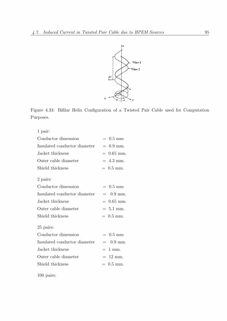
4.7. Induced Current in Twisted Pair Cable due to HPEM Sources 95
Figure 4.33: Bifilar Helix Configuration of a Twisted Pair Cable used for Computation
Purposes.
1 pair:
Conductor dimension = 0.5 mm
Insulated conductor diameter = 0.9 mm.
Jacket thickness = 0.65 mm.
Outer cable diameter = 4.3 mm.
Shield thickness = 0.5 mm.
2 pairs:
Conductor dimension = 0.5 mm
Insulated conductor diameter = 0.9 mm.
Jacket thickness = 0.65 mm.
Outer cable diameter = 5.1 mm.
Shield thickness = 0.5 mm.
25 pairs:
Conductor dimension = 0.5 mm
Insulated conductor diameter = 0.9 mm.
Jacket thickness = 1 mm.
Outer cable diameter = 12 mm.
Shield thickness = 0.5 mm.
100 pairs:
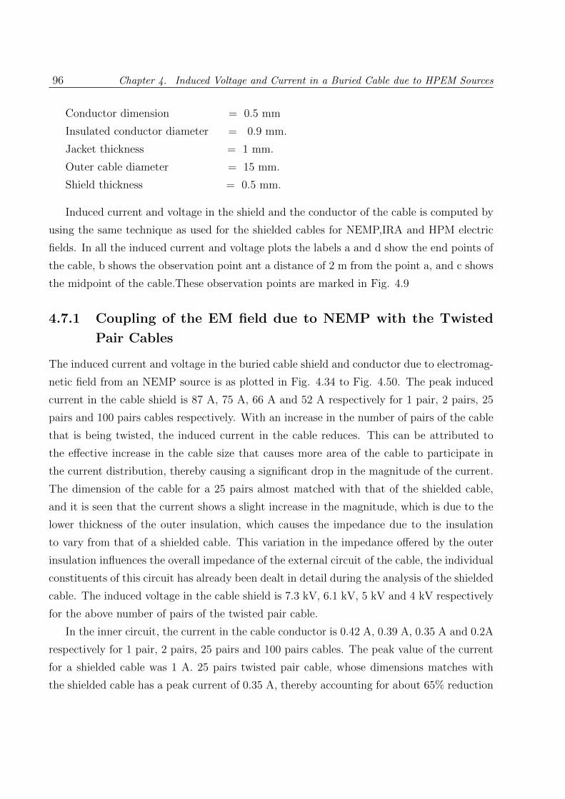
96 Chapter 4. Induced Voltage and Current in a Buried Cable due to HPEM Sources
Conductor dimension = 0.5 mm
Insulated conductor diameter = 0.9 mm.
Jacket thickness = 1 mm.
Outer cable diameter = 15 mm.
Shield thickness = 0.5 mm.
Induced current and voltage in the shield and the conductor of the cable is computed by
using the same technique as used for the shielded cables for NEMP,IRA and HPM electric
fields. In all the induced current and voltage plots the labels a and d show the end points of
the cable, b shows the observation point ant a distance of 2 m from the point a, and c shows
the midpoint of the cable.These observation points are marked in Fig. 4.9
4.7.1 Coupling of the EM field due to NEMP with the Twisted
Pair Cables
The induced current and voltage in the buried cable shield and conductor due to electromag-
netic field from an NEMP source is as plotted in Fig. 4.34 to Fig. 4.50. The peak induced
current in the cable shield is 87 A, 75 A, 66 A and 52 A respectively for 1 pair, 2 pairs, 25
pairs and 100 pairs cables respectively. With an increase in the number of pairs of the cable
that is being twisted, the induced current in the cable reduces. This can be attributed to
the effective increase in the cable size that causes more area of the cable to participate in
the current distribution, thereby causing a significant drop in the magnitude of the current.
The dimension of the cable for a 25 pairs almost matched with that of the shielded cable,
and it is seen that the current shows a slight increase in the magnitude, which is due to the
lower thickness of the outer insulation, which causes the impedance due to the insulation
to vary from that of a shielded cable. This variation in the impedance offered by the outer
insulation influences the overall impedance of the external circuit of the cable, the individual
constituents of this circuit has already been dealt in detail during the analysis of the shielded
cable. The induced voltage in the cable shield is 7.3 kV, 6.1 kV, 5 kV and 4 kV respectively
for the above number of pairs of the twisted pair cable.
In the inner circuit, the current in the cable conductor is 0.42 A, 0.39 A, 0.35 A and 0.2A
respectively for 1 pair, 2 pairs, 25 pairs and 100 pairs cables. The peak value of the current
for a shielded cable was 1 A. 25 pairs twisted pair cable, whose dimensions matches with
the shielded cable has a peak current of 0.35 A, thereby accounting for about 65% reduction

4.7. Induced Current in Twisted Pair Cable due to HPEM Sources 97
in the magnitude of the current. This reduction in the current is due to the twisting of the
conductors in a twisted pair cable that will cause cancellation of the current on account of
the inductive effects.
The change in the pitching of the twisted pair cable affects the induced current consid-
erably. The pitching is varied from one to 10 times the diameter, d and the induced current
is computed. As the diameter is varied the current increases and it saturates at 4.5d, where
d = diameter. Any further change in the pitching has negligible effect on the current. This
is because once the pitching is higher, then the twisting will not have its effect and hence
the current remains unaffected. But on the lower side, any decrease in the pitching will
make a more tightly twisted cable, which will cause the mutually coupled components of the
currents to get cancelled and hence the net current drops.
4.7.2 Coupling due to IRA Electric Field
Electric field due to IRA couples with the twisted pair cable in a manner similar to that of
NEMP. The peak current induced in the cable shield are 180 A, 160 A, 140 A and 175 A
respectively for the 1, 2, 25 and 100 pairs of cables in the shield. This plot is shown in Fig.
4.51, Fig. 4.55, Fig. 4.59 and Fig. 4.63 respectively. In the conductor these currents are 2.1
A, 2 A, 1.5 A and 1.3 A for the above pairs of the cable. These respective plots are shown
in Fig. 4.52, Fig. 4.56, Fig. 4.60 and Fig. 4.64.
The induced voltage in the cable shield is 15 kV, 12 kV, 11 kV and 9 kV respectively and
is plotted in Fig. 4.53, Fig. 4.57, Fig. 4.61 and Fig. 4.65 and in the conductor these are 160
V, 130 V, 100 V and 80 V respectively and are shown in Fig. 4.54, Fig. 4.58, Fig. 4.62 and
Fig. 4.66. The peak value of the induced current in the conductor is plotted as a function
of the pitching of the cable in Fig. 4.67. In contrast to the current due to an NEMP, where
there is a large gap between the 25 pair and 100 pair and almost equal gap between the
remaining pairs, in the IRA the gap between the current plots are almost equal. This is due
to the fact that the mutual coupling eliminates certain frequency components in the current
induced due to EM field from an IRA, which are mainly the high frequency components.
Again this is only a function of the pitching. The variation in the cable diameter affects
less as compared to NEMP because the shield thickness is the same, and only the insulation
thickness varies and because of the skin effect, this variation is only less affected in the output
current. The induced current drops by 40% for 25 pair cable from the current magnitude
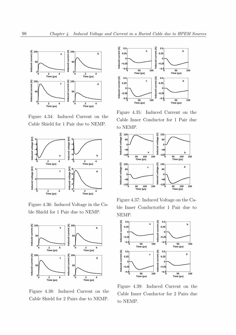
98 Chapter 4. Induced Voltage and Current in a Buried Cable due to HPEM Sources
0 2 40
50
100
Time (µs)
Indu
ced
curr
ent (
A)
0 2 40
50
100
Time (µs)
Indu
ced
curr
ent (
A)
0 2 40
50
100
Time (µs)
Indu
ced
curr
ent (
A)
0 2 40
50
100
Time (µs)
Indu
ced
curr
ent (
A)
a
c d
b
Figure 4.34: Induced Current on the
Cable Shield for 1 Pair due to NEMP.
0 50 100−0.5
−0.25
0
0.25
0.5
Time (µs)
Indu
ced
curr
ent (
A)
0 50 100−0.5
−0.25
0
0.25
0.5
Time (µs)
Indu
ced
curr
ent (
A)
0 50 100−0.5
−0.25
0
0.25
0.5
Time (µs)
Indu
ced
curr
ent (
A)
0 50 100−0.5
−0.25
0
0.25
0.5
Time (µs)
Indu
ced
curr
ent (
A)
ba
dc
Figure 4.35: Induced Current on the
Cable Inner Conductor for 1 Pair due
to NEMP.
0 2 4−8
−6
−4
−2
0
Time (µs)
Indu
ced
volta
ge (
kV)
0 2 4−8
−6
−4
−2
0
Time (µs)
Indu
ced
volta
ge (
kV)
0 2 4−1
0
1
Time (µs)
Indu
ced
volta
ge (
kV)
0 2 40
2
4
6
8
Time (µs)
Indu
ced
volta
ge (
kV)
a
c
b
d
Figure 4.36: Induced Voltage in the Ca-
ble Shield for 1 Pair due to NEMP.
0 50 100 150−120
−60
0
60
120
Time (µs)
Indu
ced
volta
ge (
V)
0 50 100 150−120
−60
0
60
120
Time (µs)In
duce
d vo
ltage
(V
)
0 50 100 150−120
−60
0
60
120
Time (µs)
Indu
ced
volta
ge (
V)
0 50 100 150−120
−60
0
60
120
Time (µs)
Indu
ced
volta
ge (
V)
a b
c d
Figure 4.37: Induced Voltage on the Ca-
ble Inner Conductorfor 1 Pair due to
NEMP.
0 2 40
50
100
Time (µs)
Indu
ced
curr
ent (
A)
0 2 40
50
100
Time (µs)
Indu
ced
curr
ent (
A)
0 2 40
50
100
Time (µs)
Indu
ced
curr
ent (
A)
0 2 40
50
100
Time (µs)
Indu
ced
curr
ent (
A)
a
c
b
d
Figure 4.38: Induced Current on the
Cable Shield for 2 Pairs due to NEMP.
0 50 100−0.5
−0.25
0
0.25
0.5
Time (µs)
Indu
ced
curr
ent (
A)
0 50 100−0.5
−0.25
0
0.25
0.5
Time (µs)
Indu
ced
curr
ent (
A)
0 50 100−0.5
−0.25
0
0.25
0.5
Time (µs)
Indu
ced
curr
ent (
A)
0 50 100−0.5
−0.25
0
0.25
0.5
Time (µs)
Indu
ced
curr
ent (
A)
ba
c d
Figure 4.39: Induced Current on the
Cable Inner Conductor for 2 Pairs due
to NEMP.
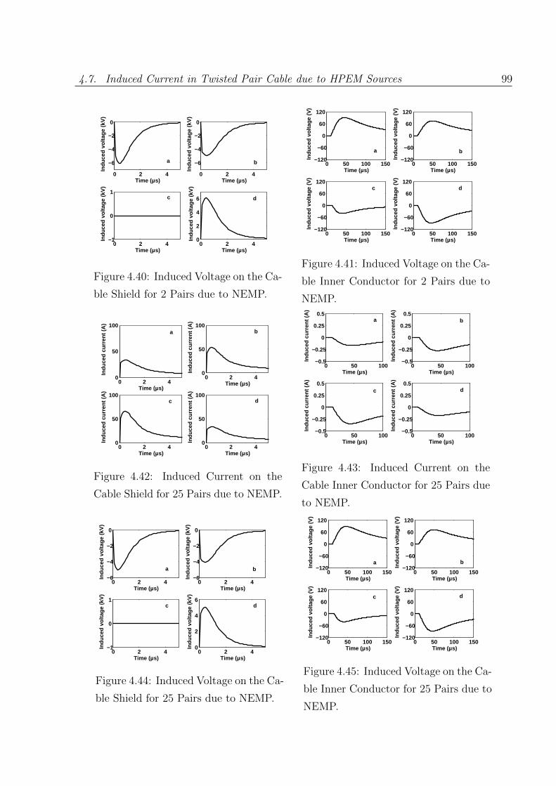
4.7. Induced Current in Twisted Pair Cable due to HPEM Sources 99
0 2 4
−6
−4
−2
0
Time (µs)
Indu
ced
volta
ge (
kV)
0 2 4
−6
−4
−2
0
Time (µs)In
duce
d vo
ltage
(kV
)
0 2 4−1
0
1
Time (µs)
Indu
ced
volta
ge (
kV)
0 2 40
2
4
6
Time (µs)
Indu
ced
volta
ge (
kV)
a
c
b
d
Figure 4.40: Induced Voltage on the Ca-
ble Shield for 2 Pairs due to NEMP.
0 50 100 150−120
−60
0
60
120
Time (µs)
Indu
ced
volta
ge (
V)
0 50 100 150−120
−60
0
60
120
Time (µs)
Indu
ced
volta
ge (
V)
0 50 100 150−120
−60
0
60
120
Time (µs)
Indu
ced
volta
ge (
V)
0 50 100 150−120
−60
0
60
120
Time (µs)
Indu
ced
volta
ge (
V)
a b
c d
Figure 4.41: Induced Voltage on the Ca-
ble Inner Conductor for 2 Pairs due to
NEMP.
0 2 40
50
100
Time (µs)
Indu
ced
curr
ent (
A)
0 2 40
50
100
Time (µs)
Indu
ced
curr
ent (
A)
0 2 40
50
100
Time (µs)
Indu
ced
curr
ent (
A)
0 2 40
50
100
Time (µs)
Indu
ced
curr
ent (
A)
a b
c d
Figure 4.42: Induced Current on the
Cable Shield for 25 Pairs due to NEMP.
0 50 100−0.5
−0.25
0
0.25
0.5
Time (µs)
Indu
ced
curr
ent (
A)
0 50 100−0.5
−0.25
0
0.25
0.5
Time (µs)
Indu
ced
curr
ent (
A)
0 50 100−0.5
−0.25
0
0.25
0.5
Time (µs)
Indu
ced
curr
ent (
A)
0 50 100−0.5
−0.25
0
0.25
0.5
Time (µs)
Indu
ced
curr
ent (
A)
a b
c d
Figure 4.43: Induced Current on the
Cable Inner Conductor for 25 Pairs due
to NEMP.
0 2 4−6
−4
−2
0
Time (µs)
Indu
ced
volta
ge (
kV)
0 2 4−6
−4
−2
0
Time (µs)
Indu
ced
volta
ge (
kV)
0 2 4−1
0
1
Time (µs)
Indu
ced
volta
ge (
kV)
0 2 40
2
4
6
Time (µs)
Indu
ced
volta
ge (
kV)
a b
c d
Figure 4.44: Induced Voltage on the Ca-
ble Shield for 25 Pairs due to NEMP.
0 50 100 150−120
−60
0
60
120
Time (µs)
Indu
ced
volta
ge (
V)
0 50 100 150−120
−60
0
60
120
Time (µs)
Indu
ced
volta
ge (
V)
0 50 100 150−120
−60
0
60
120
Time (µs)
Indu
ced
volta
ge (
V)
0 50 100 150−120
−60
0
60
120
Time (µs)
Indu
ced
volta
ge (
V)
a b
c d
Figure 4.45: Induced Voltage on the Ca-
ble Inner Conductor for 25 Pairs due to
NEMP.
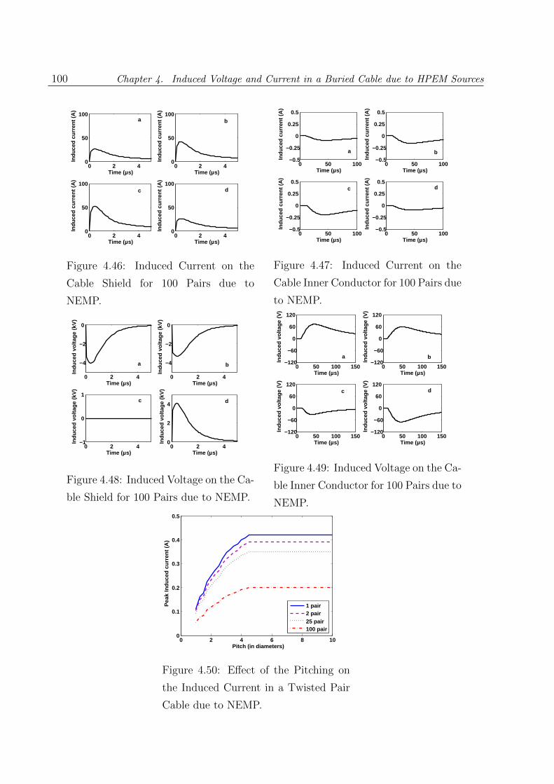
100 Chapter 4. Induced Voltage and Current in a Buried Cable due to HPEM Sources
0 2 40
50
100
Time (µs)
Indu
ced
curr
ent (
A)
0 2 40
50
100
Time (µs)
Indu
ced
curr
ent (
A)
0 2 40
50
100
Time (µs)
Indu
ced
curr
ent (
A)
0 2 40
50
100
Time (µs)
Indu
ced
curr
ent (
A)
a b
c d
Figure 4.46: Induced Current on the
Cable Shield for 100 Pairs due to
NEMP.
0 50 100−0.5
−0.25
0
0.25
0.5
Time (µs)
Indu
ced
curr
ent (
A)
0 50 100−0.5
−0.25
0
0.25
0.5
Time (µs)
Indu
ced
curr
ent (
A)
0 50 100−0.5
−0.25
0
0.25
0.5
Time (µs)
Indu
ced
curr
ent (
A)
0 50 100−0.5
−0.25
0
0.25
0.5
Time (µs)
Indu
ced
curr
ent (
A)
a b
c d
Figure 4.47: Induced Current on the
Cable Inner Conductor for 100 Pairs due
to NEMP.
0 2 4
−4
−2
0
Time (µs)
Indu
ced
volta
ge (
kV)
0 2 4
−4
−2
0
Time (µs)
Indu
ced
volta
ge (
kV)
0 2 4−1
0
1
Time (µs)
Indu
ced
volta
ge (
kV)
0 2 40
2
4
Time (µs)
Indu
ced
volta
ge (
kV)
a b
c d
Figure 4.48: Induced Voltage on the Ca-
ble Shield for 100 Pairs due to NEMP.
0 50 100 150−120
−60
0
60
120
Time (µs)
Indu
ced
volta
ge (
V)
0 50 100 150−120
−60
0
60
120
Time (µs)
Indu
ced
volta
ge (
V)
0 50 100 150−120
−60
0
60
120
Time (µs)
Indu
ced
volta
ge (
V)
0 50 100 150−120
−60
0
60
120
Time (µs)
Indu
ced
volta
ge (
V)
a b
c d
Figure 4.49: Induced Voltage on the Ca-
ble Inner Conductor for 100 Pairs due to
NEMP.
0 2 4 6 8 100
0.1
0.2
0.3
0.4
0.5
Pitch (in diameters)
Pea
k In
du
ced
cu
rren
t (A
)
1 pair2 pair25 pair100 pair
Figure 4.50: Effect of the Pitching on
the Induced Current in a Twisted Pair
Cable due to NEMP.

4.7. Induced Current in Twisted Pair Cable due to HPEM Sources 101
300 400 500 600−200
0
200
Time (ns)
Indu
ced
curr
ent (
A)
300 400 500 600−200
0
200
Time (ns)
Indu
ced
curr
ent (
A)
300 400 500−200
0
200
Time (ns)
Indu
ced
curr
ent (
A)
300 400 500 600−200
0
200
Time (ns)
Indu
ced
curr
ent (
A)
a
c
b
d
Figure 4.51: Induced Current on the
Cable Shield for 1 Pair due to EM field
from an IRA.
200 400 600 800 10001200−3
−2
−1
0
1
Time (ns)
Indu
ced
curr
ent(
A)
200 400 600 800 10001200−3
−2
−1
0
1
Time (ns)
Indu
ced
curr
ent(
A)
200 400 600 800 10001200−3
−2
−1
0
1
Time (ns)
Indu
ced
curr
ent(
A)
200 400 600 800 10001200−3
−2
−1
0
1
Time (ns)
Indu
ced
curr
ent(
A)
a b
c d
Figure 4.52: Induced Current on the
Cable Inner Conductor for 1 Pair due
to EM field from an IRA.
1600 1800 2000
−10
0
10
Time (ns)
Indu
ced
volta
ge (
kV)
1600 1800 2000
−10
0
10
Time (ns)
Indu
ced
volta
ge (
kV)
1600 1800 2000
−10
0
10
Time (ns)
Indu
ced
volta
ge (
kV)
1600 1800 2000
−10
0
10
Time (ns)
Indu
ced
volta
ge (
kV)
a
c
b
d
Figure 4.53: Induced Voltage on the Ca-
ble Shield for 1 Pair due to EM field
from an IRA.
200 400 600 800 10001200−200
−100
0
Time (ns)
Indu
ced
volta
ge (
V)
200 400 600 800 10001200−200
−100
0
Time (ns)
Indu
ced
volta
ge (
V)
200 400 600 800 10001200
0
100
200
Time (ns)
Indu
ced
volta
ge (
V)
200 400 600 800 10001200
0
100
200
Time (ns)
Indu
ced
volta
ge (
V)
a
c
b
d
Figure 4.54: Induced Voltage on the Ca-
ble Inner Conductor for 1 Pair due to
EM field from an IRA.
300 400 500 600−200
0
200
Time (ns)
Indu
ced
curr
ent (
A)
300 400 500 600−200
0
200
Time (ns)
Indu
ced
curr
ent (
A)
300 400 500−200
0
200
Time (ns)
Indu
ced
curr
ent (
A)
300 400 500 600−200
0
200
Time (ns)
Indu
ced
curr
ent (
A)
a
c
b
d
Figure 4.55: Induced Voltage on the Ca-
ble Inner Conductor for 1 Pair due to
EM field from an IRA.
200 400 600 800 10001200−3
−2
−1
0
1
Time (ns)
Indu
ced
curr
ent(
A)
200 400 600 800 10001200−3
−2
−1
0
1
Time (ns)
Indu
ced
curr
ent(
A)
200 400 600 800 10001200−3
−2
−1
0
1
Time (ns)
Indu
ced
curr
ent(
A)
200 400 600 800 10001200−3
−2
−1
0
1
Time (ns)
Indu
ced
curr
ent(
A)
a
c
b
d
Figure 4.56: Induced Current on the
Cable Inner Conductor for 2 Pairs due
to EM field from an IRA.
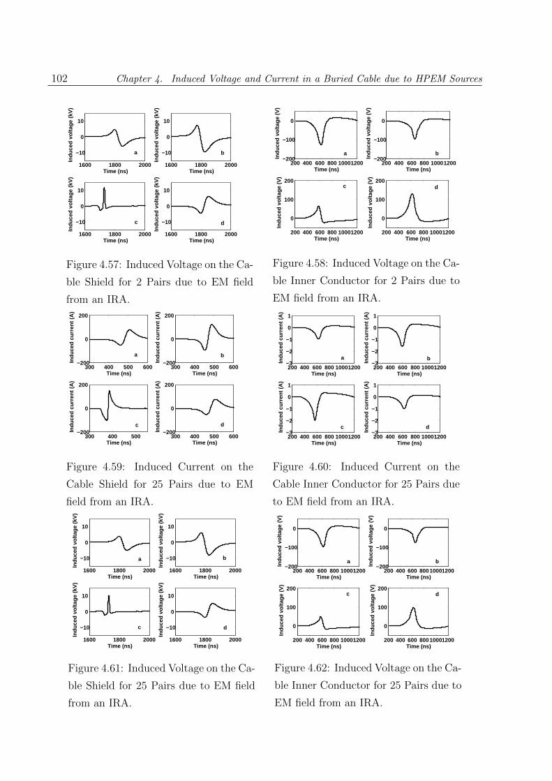
102 Chapter 4. Induced Voltage and Current in a Buried Cable due to HPEM Sources
1600 1800 2000
−10
0
10
Time (ns)
Indu
ced
volta
ge (
kV)
1600 1800 2000
−10
0
10
Time (ns)
Indu
ced
volta
ge (
kV)
1600 1800 2000
−10
0
10
Time (ns)
Indu
ced
volta
ge (
kV)
1600 1800 2000
−10
0
10
Time (ns)
Indu
ced
volta
ge (
kV)
a
c
b
d
Figure 4.57: Induced Voltage on the Ca-
ble Shield for 2 Pairs due to EM field
from an IRA.
200 400 600 800 10001200−200
−100
0
Time (ns)
Indu
ced
volta
ge (
V)
200 400 600 800 10001200−200
−100
0
Time (ns)
Indu
ced
volta
ge (
V)
200 400 600 800 10001200
0
100
200
Time (ns)
Indu
ced
volta
ge (
V)
200 400 600 800 10001200
0
100
200
Time (ns)
Indu
ced
volta
ge (
V)
a
c
b
d
Figure 4.58: Induced Voltage on the Ca-
ble Inner Conductor for 2 Pairs due to
EM field from an IRA.
300 400 500 600−200
0
200
Time (ns)
Indu
ced
curr
ent (
A)
300 400 500 600−200
0
200
Time (ns)
Indu
ced
curr
ent (
A)
300 400 500−200
0
200
Time (ns)
Indu
ced
curr
ent (
A)
300 400 500 600−200
0
200
Time (ns)
Indu
ced
curr
ent (
A)
a
c
b
d
Figure 4.59: Induced Current on the
Cable Shield for 25 Pairs due to EM
field from an IRA.
200 400 600 800 10001200−3
−2
−1
0
1
Time (ns)
Indu
ced
curr
ent (
A)
200 400 600 800 10001200−3
−2
−1
0
1
Time (ns)
Indu
ced
curr
ent (
A)
200 400 600 800 10001200−3
−2
−1
0
1
Time (ns)
Indu
ced
curr
ent (
A)
200 400 600 800 10001200−3
−2
−1
0
1
Time (ns)
Indu
ced
curr
ent (
A)
a b
c d
Figure 4.60: Induced Current on the
Cable Inner Conductor for 25 Pairs due
to EM field from an IRA.
1600 1800 2000
−10
0
10
Time (ns)
Indu
ced
volta
ge (
kV)
1600 1800 2000
−10
0
10
Time (ns)
Indu
ced
volta
ge (
kV)
1600 1800 2000
−10
0
10
Time (ns)
Indu
ced
volta
ge (
kV)
1600 1800 2000
−10
0
10
Time (ns)
Indu
ced
volta
ge (
kV)
a
c
b
d
Figure 4.61: Induced Voltage on the Ca-
ble Shield for 25 Pairs due to EM field
from an IRA.
200 400 600 800 10001200−200
−100
0
Time (ns)
Indu
ced
volta
ge (
V)
200 400 600 800 10001200−200
−100
0
Time (ns)
Indu
ced
volta
ge (
V)
200 400 600 800 10001200
0
100
200
Time (ns)
Indu
ced
volta
ge (
V)
200 400 600 800 10001200
0
100
200
Time (ns)
Indu
ced
volta
ge (
V)
a
c
b
d
Figure 4.62: Induced Voltage on the Ca-
ble Inner Conductor for 25 Pairs due to
EM field from an IRA.

4.8. Chapter Summary 103
for a shielded cable
4.7.3 Coupling due to HPM Electric Field
Electric field due to IRA couples with the twisted pair cable in a manner similar to that
of NEMP. The peak currents induced on the cable shield are 515 A, 510 A, 505 A and 502
A respectively for the 1, 2, 25 and 100 pairs of cables in the shield. These waveforms are
shown in Fig. 4.68, Fig. 4.72, Fig. 4.76 and Fig. 4.80 respectively. On the inner conductor,
these induced currents are 8 A, 7 A, 5 A and 3.5 A for the above pairs of the cable. The
respective plots are shown in Fig. 4.69, Fig. 4.73, Fig. 4.77, and Fig. 4.81.
The induced voltage in the cable shield is 60 kV, 50 kV, 35 kV and 30 kV respectively
and are plotted in Fig. 4.70, Fig. 4.74, Fig. 4.78 and Fig. 4.82 and on the inner conductor
these are 580 V, 560 V, 540 V and 500 V respectively which are shown in Fig. 4.71, Fig.
4.75, Fig. 4.79 and Fig. 4.83. The peak value of the induced current in the conductor is
plotted as a function of the pitching of the cable in Fig. 4.84. In the case of HPM, the gap
between the currents of 1 and 2 pair is the smallest as compared to the other sources. This
is because the variation in the conductor dimension is only 0.2 mm in the outer diameter
which has negligible influence on a high frequency signal, because of the skin effect. The
percentage variation of the induced current from the shielded cable to the twisted pair cable
of 25 pair is 37.5%.
4.8 Chapter Summary
This chapter deals with the computation of the induced current and voltage in a buried
cable. Two types of cables are considered - shielded cable and twisted pair cable. For the
computation, the Enhanced Transmission Line Model has been used which is explained in
the chapter. The validation of the present model is done with the help of NEC - 4 full wave
analysis and the results are found to be closely matching. The following conclusions are
arrived from this chapter:
• The induced current is more for a shielded cable than a twisted pair cable of the same
configuration.)
• The induced current magnitude depends upon the type of the HPEM source, the depth
of burial of the cable and the point on the cable where the current/ voltage is computed.

104 Chapter 4. Induced Voltage and Current in a Buried Cable due to HPEM Sources
300 400 500 600−200
0
200
Time (ns)
Indu
ced
curr
ent (
A)
300 400 500 600−200
0
200
Time (ns)
Indu
ced
curr
ent (
A)
300 400 500−200
0
200
Time (ns)
Indu
ced
curr
ent (
A)
300 400 500 600−200
0
200
Time (ns)
Indu
ced
curr
ent (
A)
a
c
b
d
Figure 4.63: Induced Voltage on the Ca-
ble Inner Conductor for 25 Pairs due to
EM field from an IRA.
200 400 600 800 10001200−3
−2
−1
0
1
Time (ns)
Indu
ced
curr
ent (
A)
200 400 600 800 10001200−3
−2
−1
0
1
Time (ns)
Indu
ced
curr
ent (
A)
200 400 600 800 10001200−3
−2
−1
0
1
Time (ns)
Indu
ced
curr
ent (
A)
200 400 600 800 10001200−3
−2
−1
0
1
Time (ns)
Indu
ced
curr
ent (
A)
a b
c d
Figure 4.64: Induced Current on the
Cable Inner Conductor for 100 Pairs due
to EM field from an IRA.
1600 1800 2000
−10
0
10
Time (ns)
Indu
ced
volta
ge (
kV)
1600 1800 2000
−10
0
10
Time (ns)
Indu
ced
volta
ge (
kV)
1600 1800 2000
−10
0
10
Time (ns)
Indu
ced
volta
ge (
kV)
1600 1800 2000
−10
0
10
Time (ns)
Indu
ced
volta
ge (
kV)
a
c
b
d
Figure 4.65: Induced Voltage on the Ca-
ble Shield for 100 Pairs due to EM field
from an IRA.
200 400 600 800 10001200−200
−100
0
Time (ns)
Indu
ced
volta
ge (
V)
200 400 600 800 10001200−200
−100
0
Time (ns)In
duce
d vo
ltage
(V
)
200 400 600 800 10001200
0
100
200
Time (ns)
Indu
ced
volta
ge (
V)
200 400 600 800 10001200
0
100
200
Time (ns)
Indu
ced
volta
ge (
V)
a b
c d
Figure 4.66: Induced Voltage on the Ca-
ble Inner Conductor for 100 Pairs due to
EM field from an IRA.
0 2 4 6 8 100
0.5
1
1.5
2
2.5
Pitch (in diameters)
Pea
k In
du
ced
cu
rren
t (A
)
1 pair2 pair25 pair100 pair
Figure 4.67: Effect of the Pitching on
the Induced Current in a Twisted Pair
Cable due to EM field from an IRA.

4.8. Chapter Summary 105
1710 1715 1720 1725
−500
0
500
Time (ns)
Indu
ced
curr
ent (
A)
1700 1705 1710
−500
0
500
Time (ns)
Indu
ced
curr
ent (
A)
1685 1690 1695
−500
0
500
Time (ns)
Indu
ced
curr
ent (
A)
1710 1715 1720 1725
−500
0
500
Time (ns)
Indu
ced
curr
ent (
A)
a b
dc
Figure 4.68: Induced Current on the
Cable Shield for 1 Pair due to EM field
from an HPM Source.
400 600 800−10
−5
0
Time (ns)
Indu
ced
curr
ent (
A)
400 600 800−10
−5
0
Time (ns)
Indu
ced
curr
ent (
A)
400 600 800−10
−5
0
Time (ns)
Indu
ced
curr
ent (
A)
400 600 800−10
−5
0
Time (ns)
Indu
ced
curr
ent (
A)
a
c d
b
Figure 4.69: Induced Current on the
Cable Inner Conductor for 1 Pair due
to EM field from an HPM Source.
370 375 380
−50
0
50
Time (ns)
Indu
ced
volta
ge (
kV)
355 360 365
−50
0
50
Time (ns)
Indu
ced
volta
ge (
kV)
340 345 350
−50
0
50
Time (ns)
Indu
ced
volta
ge (
kV)
370 375 380
−50
0
50
Time (ns)
Indu
ced
volta
ge (
kV)
a
c
b
d
Figure 4.70: Induced Voltage on the Ca-
ble Shield for 1 Pair due to EM field
from an HPM Source.
400 600 800−600
−300
0
300
600
Time (ns)
Indu
ced
volta
ge (
V)
400 600 800−600
−300
0
300
600
Time (ns)
Indu
ced
volta
ge (
V)
400 600 800−600
−300
0
300
600
Time (ns)
Indu
ced
volta
ge (
V)
400 600 800−600
−300
0
300
600
Time (ns)
Indu
ced
volta
ge (
V)
a
dc
b
Figure 4.71: Induced Voltage on the Ca-
ble Inner Conductor for 1 Pair due to
EM field from an HPM Source.
1710 1715 1720 1725
−500
0
500
Time (ns)
Indu
ced
curr
ent (
A)
1700 1705 1710
−500
0
500
Time (ns)
Indu
ced
curr
ent (
A)
1685 1690 1695
−500
0
500
Time (ns)
Indu
ced
curr
ent (
A)
1710 1715 1720 1725
−500
0
500
Time (ns)
Indu
ced
curr
ent (
A)
a
c d
b
Figure 4.72: Induced Current on the
Cable Shield for 2 Pairs due to EM field
from an HPM Source.
400 600 800−10
−5
0
Time (ns)
Indu
ced
curr
ent (
A)
400 600 800−10
−5
0
Time (ns)
Indu
ced
curr
ent (
A)
400 600 800−10
−5
0
Time (ns)
Indu
ced
curr
ent (
A)
400 600 800−10
−5
0
Time (ns)
Indu
ced
curr
ent (
A)
a
c
b
d
Figure 4.73: Induced Current on the
Cable Inner Conductor for 2 Pairs due
to EM field from an HPM Source.

106 Chapter 4. Induced Voltage and Current in a Buried Cable due to HPEM Sources
370 375 380
−50
0
50
Time (ns)
Indu
ced
volta
ge (
kV)
355 360 365
−50
0
50
Time (ns)
Indu
ced
volta
ge (
kV)
340 345 350
−50
0
50
Time (ns)
Indu
ced
volta
ge (
kV)
370 375 380
−50
0
50
Time (ns)
Indu
ced
volta
ge (
kV)
a
c
b
d
Figure 4.74: Induced Voltage on the Ca-
ble Shield for 2 Pairs due to EM field
from an HPM Source.
400 600 800−600
−300
0
300
600
Time (ns)
Indu
ced
volta
ge (
V)
400 600 800−600
−300
0
300
600
Time (ns)
Indu
ced
volta
ge (
V)
400 600 800−600
−300
0
300
600
Time (ns)
Indu
ced
volta
ge (
V)
400 600 800−600
−300
0
300
600
Time (ns)
Indu
ced
volta
ge (
V)
a
c
b
d
Figure 4.75: Induced Voltage on the Ca-
ble Inner Conductor for 2 Pairs due to
EM field from an HPM Source.
1710 1715 1720 1725
−500
0
500
Time (ns)
Indu
ced
curr
ent (
A)
1700 1705 1710
−500
0
500
Time (ns)
Indu
ced
curr
ent (
A)
1685 1690 1695
−500
0
500
Time (ns)
Indu
ced
curr
ent (
A)
1710 1715 1720 1725
−500
0
500
Time (ns)
Indu
ced
curr
ent (
A)
a b
c d
Figure 4.76: Induced Current on the
Cable Shield for 25 Pairs due to EM
field from an HPM Source.
400 600 800−10
−5
0
Time (ns)
Indu
ced
curr
ent (
A)
400 600 800−10
−5
0
Time (ns)
Indu
ced
curr
ent (
A)
400 600 800−10
−5
0
Time (ns)
Indu
ced
curr
ent (
A)
400 600 800−10
−5
0
Time (ns)
Indu
ced
curr
ent (
A)
a b
c d
Figure 4.77: Induced Current on the
Cable Inner Conductor for 25 Pairs due
to EM field from an HPM Source.
370 375 380−50
0
50
Time (ns)
Indu
ced
volta
ge (
kV)
355 360 365−50
0
50
Time (ns)
Indu
ced
volta
ge (
kV)
340 345 350−50
0
50
Time (ns)
Indu
ced
volta
ge (
kV)
370 375 380−50
0
50
Time (ns)
Indu
ced
volta
ge (
kV)
a
c
b
d
Figure 4.78: Induced Voltage on the Ca-
ble Shield for 25 Pairs due to EM field
from an HPM Source.
400 600 800−600
−300
0
300
600
Time (ns)
Indu
ced
volta
ge (
V)
400 600 800−600
−300
0
300
600
Time (ns)
Indu
ced
volta
ge (
V)
400 600 800−600
−300
0
300
600
Time (ns)
Indu
ced
volta
ge (
V)
400 600 800−600
−300
0
300
600
Time (ns)
Indu
ced
volta
ge (
V)
a
c
b
d
Figure 4.79: Induced Voltage on the Ca-
ble Inner Conductor for 25 Pairs due to
EM field from an HPM Source.

4.8. Chapter Summary 107
1710 1715 1720 1725
−500
0
500
Time (ns)
Indu
ced
curr
ent (
A)
1700 1705 1710
−500
0
500
Time (ns)
Indu
ced
curr
ent (
A)
1685 1690 1695
−500
0
500
Time (ns)
Indu
ced
curr
ent (
A)
1710 1715 1720 1725
−500
0
500
Time (ns)
Indu
ced
curr
ent (
A)
a
c
b
d
Figure 4.80: Induced Current on the
Cable Shield for 100 Pairs due to EM
field from an HPM Source.
400 600 800−10
−5
0
Time (ns)
Indu
ced
curr
ent (
A)
400 600 800−10
−5
0
Time (ns)
Indu
ced
curr
ent (
A)
400 600 800−10
−5
0
Time (ns)
Indu
ced
curr
ent (
A)
400 600 800−10
−5
0
Time (ns)
Indu
ced
curr
ent (
A)
a
c d
b
Figure 4.81: Induced Current on the
Cable Inner Conductor for 100 Pairs due
to EM field from an HPM Source.
370 375 380−50
0
50
Time (ns)
Indu
ced
volta
ge (
kV)
355 360 365−50
0
50
Time (ns)
Indu
ced
volta
ge (
kV)
340 345 350−50
0
50
Time (ns)
Indu
ced
volta
ge (
kV)
370 375 380−50
0
50
Time (ns)
Indu
ced
volta
ge (
kV)
a
c
b
d
Figure 4.82: Induced Voltage on the Ca-
ble Shield for 100 Pairs due to EM field
from an HPM Source.
400 600 800−600
−300
0
300
600
Time (ns)
Indu
ced
volta
ge (
V)
400 600 800−600
−300
0
300
600
Time (ns)
Indu
ced
volta
ge (
V)
400 600 800−600
−300
0
300
600
Time (ns)
Indu
ced
volta
ge (
V)
400 600 800−600
−300
0
300
600
Time (ns)
Indu
ced
volta
ge (
V)
a
c d
b
Figure 4.83: Induced Voltage on the Ca-
ble Inner Conductor for 100 Pairs due to
EM field from an HPM Source.
0 2 4 6 8 100
2
4
6
8
10
Pitch (in diameters)
Pea
k In
du
ced
cu
rren
t (A
)
1pair 2 pair25 pair100 pair
Figure 4.84: Effect of the Pitching on
the Induced Current in a Twisted Pair
Cable due to EM field from an HPM
Source.

108 Chapter 4. Induced Voltage and Current in a Buried Cable due to HPEM Sources
• Current is maximum at the centre of the cable for matched terminations and the
voltage is the minimum at this point.
• The percentage of the induced current in the inner conductor with respect to the shield
current of a shielded cable is the least for an HPM, then comes the IRA and finally
the NEMP. This is due to the fact that higher frequencies are absorbed more by the
shield of the cable. This affects the induced currents due to HPM the maximum and
NEMP the least because of the presence of the lower frequency components in NEMP.
• Induced current in the twisted pair cable depends upon the number of pairs of the
cable and the pitching of the cable for a given HPEM source.
• The percentage variation in the current between the induced currents in the shielded
and twisted pair cable is 67% for the NEMP, 40% for IRA and 37.5% for the HPM.
This is due to the fact that the smaller variations in the conductor dimensions are
negligible for frequencies in the GHz range.
• The twisted pair cable of pitching equal to 4.5 times the diameter shows the saturation
limit of the induced current. With decrease in the pitching below this value will cause
current to reduce proportionately. This can be attributed to the reduction of the
mutually induced currents when the twisting becomes tighter.

Chapter 5
Coupling of the Field from an HPEM
Source with an Airborne Vehicle in
Flight
5.1 Introduction
The electromagnetic field from the HPEM sources propagate with less attenuation in the air
as compared to soil due to the lower resistance this medium offers for electromagnetic wave
propagation. Hence any airborne system in its vicinity will be subjected to intense illumi-
nation by these electromagnetic fields. Hence in this chapter, the influence of the radiated
electromagnetic fields from HPEM sources on an airborne vehicle in flight is analysed.
Airborne vehicle and its payload are extremely expensive that any damage or loss of these
as a result of the voltages and currents induced on the vehicle on account of the incident
intense HPEM electromagnetic fields can be quite undesirable. The incident electromagnetic
fields will polarize the vehicle along its axis which results in the induction of currents and
voltages. These currents and voltages will get coupled with the internal control circuits that
are extremely sensitive to such transient voltage and current pulses [99]. If the induced
voltage/ current magnitude happens to be above the damage threshold level of these circuits
then it will result in either a malfunction of the circuit or a permanent damage to it with
either of them being detrimental to the vehicle. This will even result in the abortion of
the mission or possible degradation of the vehicle performance. Hence it is worthwhile to
see the effect of an incoming HPEM electromagnetic field on the airborne vehicle with and
without the presence of its exhaust plume. For this initially plume has to be modelled
electromagnetically. Then the induced current and voltage in the vehicle is computed for
109
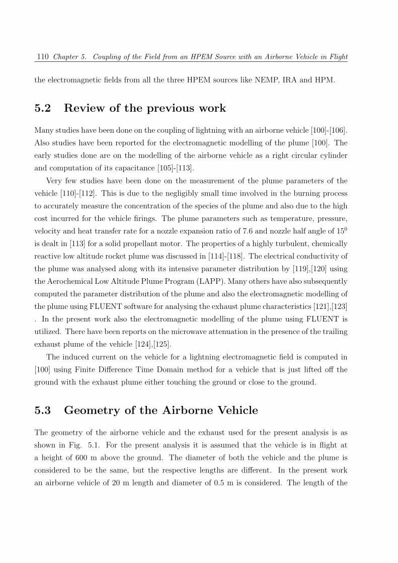
110 Chapter 5. Coupling of the Field from an HPEM Source with an Airborne Vehicle in Flight
the electromagnetic fields from all the three HPEM sources like NEMP, IRA and HPM.
5.2 Review of the previous work
Many studies have been done on the coupling of lightning with an airborne vehicle [100]-[106].
Also studies have been reported for the electromagnetic modelling of the plume [100]. The
early studies done are on the modelling of the airborne vehicle as a right circular cylinder
and computation of its capacitance [105]-[113].
Very few studies have been done on the measurement of the plume parameters of the
vehicle [110]-[112]. This is due to the negligibly small time involved in the burning process
to accurately measure the concentration of the species of the plume and also due to the high
cost incurred for the vehicle firings. The plume parameters such as temperature, pressure,
velocity and heat transfer rate for a nozzle expansion ratio of 7.6 and nozzle half angle of 150
is dealt in [113] for a solid propellant motor. The properties of a highly turbulent, chemically
reactive low altitude rocket plume was discussed in [114]-[118]. The electrical conductivity of
the plume was analysed along with its intensive parameter distribution by [119],[120] using
the Aerochemical Low Altitude Plume Program (LAPP). Many others have also subsequently
computed the parameter distribution of the plume and also the electromagnetic modelling of
the plume using FLUENT software for analysing the exhaust plume characteristics [121],[123]
. In the present work also the electromagnetic modelling of the plume using FLUENT is
utilized. There have been reports on the microwave attenuation in the presence of the trailing
exhaust plume of the vehicle [124],[125].
The induced current on the vehicle for a lightning electromagnetic field is computed in
[100] using Finite Difference Time Domain method for a vehicle that is just lifted off the
ground with the exhaust plume either touching the ground or close to the ground.
5.3 Geometry of the Airborne Vehicle
The geometry of the airborne vehicle and the exhaust used for the present analysis is as
shown in Fig. 5.1. For the present analysis it is assumed that the vehicle is in flight at
a height of 600 m above the ground. The diameter of both the vehicle and the plume is
considered to be the same, but the respective lengths are different. In the present work
an airborne vehicle of 20 m length and diameter of 0.5 m is considered. The length of the
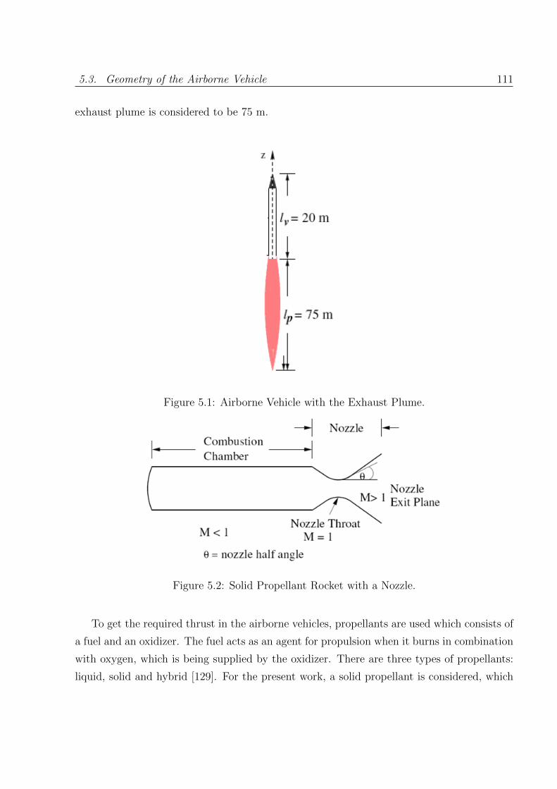
5.3. Geometry of the Airborne Vehicle 111
exhaust plume is considered to be 75 m.
Figure 5.1: Airborne Vehicle with the Exhaust Plume.
Figure 5.2: Solid Propellant Rocket with a Nozzle.
To get the required thrust in the airborne vehicles, propellants are used which consists of
a fuel and an oxidizer. The fuel acts as an agent for propulsion when it burns in combination
with oxygen, which is being supplied by the oxidizer. There are three types of propellants:
liquid, solid and hybrid [129]. For the present work, a solid propellant is considered, which
112 Chapter 5. Coupling of the Field from an HPEM Source with an Airborne Vehicle in Flight
is HTPB/AP/Al, where HTPB is Hydroxyl Terminated Polybutadiene, AP- Ammonium
Perchlorate (NH4ClO4) and Al is Aluminium. Ammonium Perchlorate (AP) is a finely
ground mineral salt which is used as the oxidizer that constitutes approximately 60-90% of
the propellant. The fuel used is aluminium which is added along with the mixture, which
increases the density and temperature of the exhaust plume. The propellant is held together
by polymeric binders such as polybutadienes, HTPB which is also consumed as fuel. These
propellants will look like rubber in its final form. A solid propellant motor with a nozzle is
shown in the Fig. 5.2. The characteristics of this solid propellant is flame tempertaure of 34400K, density of 1854.552 kg/m3 and a metal content of 4-17 wt %. When combustion occurs,
a supersonic exhaust plume is initiated from the highly compressed air in the combustion
chamber and expands through the nozzle. The composition of the solid propellant used is
given in the table 5.1.
5.4 Modeling of the Exhaust Plume
The coupling of the HPEM electric field with the airborne vehicles requires the accurate
modelling of the exhaust plume [128]-[130]. This modeling is aimed at determining the
electrical parameters of the plume such as the electrical conductivity and permittivity. These
parameters of the plume depend upon the properties of the plume such as the pressure,
temperature, species concentration and the velocity of the exhaust plume. Hence to get
the conductivity and permittivity of the plume, these intensive properties of the plume are
computed at two different sections- one inside the combustion chamber upto the nozzle
throat and second the exterior to the nozzle which is the ambient temperature where the
plume comes out. In the first section the NASA Chemical Equilibrium with Application
(CEA) software is used. In the second region, the commercially available software, FLUENT,
is used for the modelling of the exhaust plume properties. The data obtained through
the first section is the input to the FLUENT software to be used in the second section.
The FLUENT software will give the characteristics of the plume such as the temperature,
pressure, velocity and the species concentration in the axial and in the radial directions in
the ambient atmosphere. The detailed analysis of these two sections is dealt in [100].

5.5. Electromagnetic Modelling of the Plume 113
Table 5.1: Composition of the Solid Propellant
Propellant Weight
(%)
Ammonium Perchlorate 79
HTPB 13
Al 8
5.5 Electromagnetic Modelling of the Plume
The electrical properties of the exhaust plume such as conductivity and permittivity depends
upon the following factors [140],[141]:
• Combustion chamber pressure
• Combustion chamber pressure
• Nozzle back pressure
• Propellant composition
• Impurity content in the propellant which initiates the ionic charge transport in the
exhaust
• The parameters of the plume:
– Temperature
– Pressure
– Shock wave
– Velocity
– Species concentration.
When combustion occurs the exhaust comes out from the combustion chamber through
the converging and the diverging nozzle. The region from the combustion chamber to the
nozzle throat where the Mach number of exhaust plume is less than 1 is the subsonic zone.
Here it is incompressible in nature. At the nozzle throat, the Mach number is 1, which is the
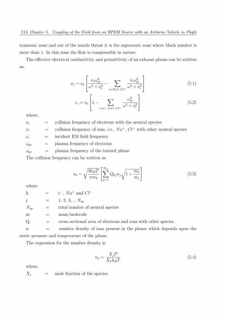
114 Chapter 5. Coupling of the Field from an HPEM Source with an Airborne Vehicle in Flight
transonic zone and out of the nozzle throat it is the supersonic zone where Mach number is
more than 1. In this zone the flow is compressible in nature.
The effective electrical conductivity and permittivity of an exhaust plume can be written
as:
σe = ε0
νeω2pe
ω2 + ν2e−
∑i=Na+,Cl−
νiω2pi
ω2 + ν2i
(5.1)
εe = ε0
1−∑
i=e−,Na+,Cl−
ω2pi
ω2 + ν2i
(5.2)
where,
νe = collision frequency of electrons with the neutral species
νi = collision frequency of ions, i.e., Na+, Cl− with other neutral species
ω = incident EM field frequency
ωpe = plasma frequency of electrons
ωpi = plasma frequency of the ionized plume
The collision frequency can be written as
νk =
√8kBT
πmk
[Nsp∑j=1
Qkjnj
√1 +
mk
mj
](5.3)
where
k = e−, Na+ and Cl−
j = 1, 2, 3, ., Nsp
Nsp = total number of neutral species
m = mass/molecule
Q = cross sectional area of electrons and ions with other species.
n = number density of ions present in the plume which depends upon the
static pressure and temperature of the plume
The expression for the number density is
nj =XjP
XTkBT(5.4)
where,
Xj = mole fraction of the species

5.6. Method of analysis used 115
XT = total mole fraction of the species
P = absolute pressure distribution.
The plasma frequency ωpk of the charged particles is
ωpk =
√nkq2kmkε0
(5.5)
where
k = e−, Na+ and Cl−
q = charge of electrons and ions
When any incoming electromagnetic field interacts with the exhaust plume it reacts with
the free electrons, free ions and heavy immobile neutral species. Since the neutral particle
does not have any interaction with the field the basic interaction of the field will be with the
electrons and ions.
The conductivity has both axial and radial variation. The mesh plot of conductivity is
shown in Fig. 5.3.
The conductivity of the missile exhaust plume along the axial position is plotted in Fig.
5.4. In this plot the maximum conductivity at each radial direction is plotted as a function
of the axial position. The conductivity starts from 0.1187 S/m and drops down to 0.02
S/m at the end point. In between these two extremities the conductivity plot shows several
oscillations at points close to the nozzle throat, where as this value drops down smoothly
after 2.1 m. This can be attributed to the intense chemical reactions taking place near
the nozzle throat that causes the conductivity to behave in a random manner, whereas it
stabilizes once the plume gets out of the nozzle premises. This behavior is also reported in
[100], where the results are closely matching.
5.6 Method of analysis used
The Finite Difference Time Domain Formulation has been used to compute the coupling of
transient electromagnetic fields with the airborne vehicle. This is a computational method
in time domain. This method has lots of disadvantages when it comes to real problem:
• This formulation requires the computation of the parameters of the airborne vehicle
like the capacitance, inductance and the resistance. This imposes a restriction on
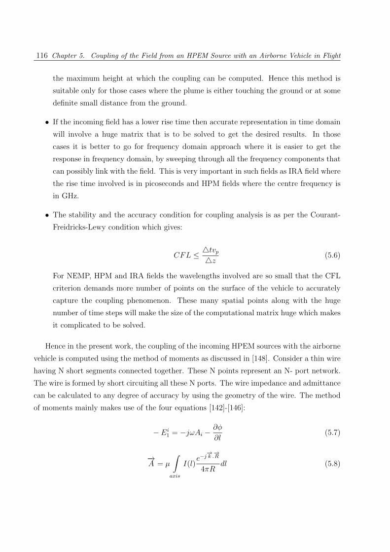
116 Chapter 5. Coupling of the Field from an HPEM Source with an Airborne Vehicle in Flight
the maximum height at which the coupling can be computed. Hence this method is
suitable only for those cases where the plume is either touching the ground or at some
definite small distance from the ground.
• If the incoming field has a lower rise time then accurate representation in time domain
will involve a huge matrix that is to be solved to get the desired results. In those
cases it is better to go for frequency domain approach where it is easier to get the
response in frequency domain, by sweeping through all the frequency components that
can possibly link with the field. This is very important in such fields as IRA field where
the rise time involved is in picoseconds and HPM fields where the centre frequency is
in GHz.
• The stability and the accuracy condition for coupling analysis is as per the Courant-
Freidricks-Lewy condition which gives:
CFL ≤ 4tvp4z
(5.6)
For NEMP, HPM and IRA fields the wavelengths involved are so small that the CFL
criterion demands more number of points on the surface of the vehicle to accurately
capture the coupling phenomenon. These many spatial points along with the huge
number of time steps will make the size of the computational matrix huge which makes
it complicated to be solved.
Hence in the present work, the coupling of the incoming HPEM sources with the airborne
vehicle is computed using the method of moments as discussed in [148]. Consider a thin wire
having N short segments connected together. These N points represent an N- port network.
The wire is formed by short circuiting all these N ports. The wire impedance and admittance
can be calculated to any degree of accuracy by using the geometry of the wire. The method
of moments mainly makes use of the four equations [142]-[146]:
− Ei1 = −jωAi −
∂φ
∂l(5.7)
−→A = µ
∫axis
I(l)e−j−→k .−→R
4πRdl (5.8)

5.6. Method of analysis used 117
φ =1
ε
∫axis
σ(l)e−j−→k .−→R
4πRdl (5.9)
σ =−1
jω
dI
dl(5.10)
where,
l = variable measured along the wire axis
R = distance measured from a source point on the axis to the field point on
the wire surface.
A = magnetic vector potential
σ = the charge density
I = current on the wire
The airborne vehicle is considered as a thin wire [147]-[154], and the method of moments
is applied to this thin wire model. This model is the best three dimensional model suited
especially if the current propagation is mainly in the axial direction. This thin wire ap-
proximation eliminates the circulating currents on the surface of the vehicle and only the
axial current needs to be considered. This thin wire model of the airborne vehicle with the
exhaust plume is as shown in the Fig. 5.5. The vehicle and the plume are modelled as thin
wire cylinders of lengths lv and lp respectively, both of radius a. The plume has an internal
impedance of Zp along the axial length of the plume, which defines the characteristics of
the plume. Zv represents the impedance of the vehicle. The incident field is EI , which
illuminates the cable. The magnitude of the field at any point along the axis of the vehicle
can be obtained from the properties of the HPEM sources that are presented in sections 2.1,
2.2 and 2.3. So the fields at different heights from the ground computed and presented in
sections 3.2 forms the source of excitation for this vehicle.
lv/2∫z′=−(lp+lv/2)
π∫φ′=0
I(z′)e−jk0R
Rdφ′dz′ = (A cos k0z +B sin k0z)
·−j2πψ0
λE0
sinθiejk0zcosθi
·j4π2
ψ0
z∫t=−(lp+lv/2)
Zi(t)I(t)sink0(z − t)dt
(5.11)
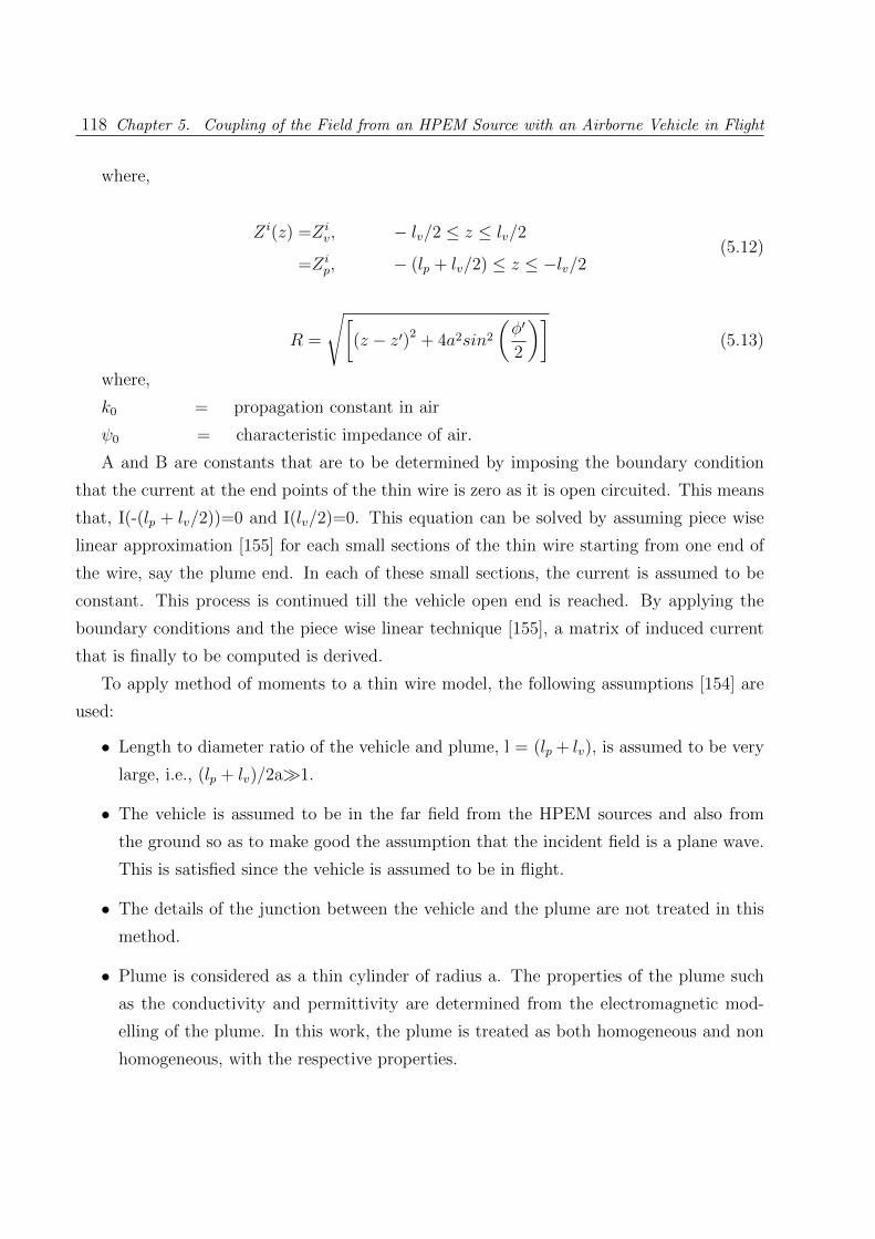
118 Chapter 5. Coupling of the Field from an HPEM Source with an Airborne Vehicle in Flight
where,
Zi(z) =Ziv, − lv/2 ≤ z ≤ lv/2
=Zip, − (lp + lv/2) ≤ z ≤ −lv/2
(5.12)
R =
√[(z − z′)2 + 4a2sin2
(φ′
2
)](5.13)
where,
k0 = propagation constant in air
ψ0 = characteristic impedance of air.
A and B are constants that are to be determined by imposing the boundary condition
that the current at the end points of the thin wire is zero as it is open circuited. This means
that, I(-(lp + lv/2))=0 and I(lv/2)=0. This equation can be solved by assuming piece wise
linear approximation [155] for each small sections of the thin wire starting from one end of
the wire, say the plume end. In each of these small sections, the current is assumed to be
constant. This process is continued till the vehicle open end is reached. By applying the
boundary conditions and the piece wise linear technique [155], a matrix of induced current
that is finally to be computed is derived.
To apply method of moments to a thin wire model, the following assumptions [154] are
used:
• Length to diameter ratio of the vehicle and plume, l = (lp + lv), is assumed to be very
large, i.e., (lp + lv)/2a1.
• The vehicle is assumed to be in the far field from the HPEM sources and also from
the ground so as to make good the assumption that the incident field is a plane wave.
This is satisfied since the vehicle is assumed to be in flight.
• The details of the junction between the vehicle and the plume are not treated in this
method.
• Plume is considered as a thin cylinder of radius a. The properties of the plume such
as the conductivity and permittivity are determined from the electromagnetic mod-
elling of the plume. In this work, the plume is treated as both homogeneous and non
homogeneous, with the respective properties.

5.6. Method of analysis used 119
Figure 5.3: Mesh Plot of the Conductivity along the Axial and Radial Direction.
0 1 2 3 4 5 6 7 80.02
0.04
0.06
0.08
0.1
0.12
Axial Position (m)
Co
nd
uct
ivit
y (S
/m)
Figure 5.4: Conductivity of the Exhaust Plume along the Axial Position.
Figure 5.5: Thin Wire Model of the Vehicle with the Exhaust Plume for Coupling Analysis.

120 Chapter 5. Coupling of the Field from an HPEM Source with an Airborne Vehicle in Flight
5.7 Validation of the Method Used
The method of moment is used to compute the induced current in a vehicle, here referred to
as a missile, and the result so obtained is compared with the results in [154] for validation.
Here the parameters for computation are:
lp = 5.54lv
Conductivity of exhaust plume = 0.25 S/m
(lp + lv)/a = l/a = 157
Conductivity of the missile (vehicle) = 3.54×10⁷ S/m
λE0 = 1
θi = 900
The electrical length of the missile 0.1 ≤ (lv/λ) ≤ 0.5
Considering that the plume is homogeneous, the induced current in the missile is com-
puted using equation 5.11 the above parameters. Computations were also repeated for the
case without the plume and the results are plotted in Fig. 5.6,Fig. 5.8, Fig. 5.10 and Fig.
5.12. The results are compared with the available results in the literature [154] as shown in
Fig. 5.7, Fig. 5.9, Fig. 5.11 and Fig. 5.13. Fig. 5.6 and Fig. 5.7 compares the induced
current on the missile at different wavelengths of the incoming field without the plume. Both
the results are closely matching and it is seen that the current builds up at the centre of
the missile and is zero at either ends. With the variation in the wavelength, current peaks
at the centre of the missile when lv/λ is close to 0.5. The frequency corresponding to this
wavelength causes resonance to occur and causes a rise in the current. When the plume is
present, the current at the tail end of the missile from where the plume starts, has some
current that is different from zero. This plot is shown in Fig. 5.8 and is compared with Fig.
5.9 which is taken from [154]. This is the effect of the finite conducting plume and hence
the current becomes zero at the bottom most point of the plume. The induced current in
the missile for two resonance lengths of the vehicle is plotted in Fig. 5.10 and Fig. 5.12.
This computed result is compared with that published by [154] as Fig. 5.11 and Fig. 5.12.
Two resonance lengths are considered, which are lv = 0.39 λ and lv = 0.09 λ. The major
observations are:
Electrically short missile:

5.8. Results and Discussions 121
The induced current in the missile is 0.06 mA. The presence of the plume causes an
increase in the current in the vehicle, and the current becomes 0.14 mA. The current is the
least at the tail end of the vehicle.
Vehicle with the length equal to resonance length:
For a vehicle with its length equal to the resonance length, the induced current in the
missile is 3.5 mA, which drops to 2.5 mA in the presence of the plume.
The current is the least at the centre of the total length of the plume and the missile and
maximum at the tail end of the missile.
Inferences:
The tail end of the vehicle has more induced current for an electrically short missile. This
is a disadvantage as it will lead to more current getting into the vehicle structure, through
the apertures that will lead to damaging the control circuits.
5.8 Results and Discussions
A sketch of the airborne vehicle used in the present work is as shown in the Fig. 5.5. The
length and radius of the vehicle are 20 m and 0.5 m respectively. The active length of the
exhaust plume is 75 m. The conductivity of the vehicle is taken as 3.54×10⁷ S/m and the
conductivity of the exhaust plume is taken from Fig. 5.4, which is computed for the whole
length of the plume. Two types of exhaust plumes are considered, one is a homogeneous
exhaust plume, where the plume conductivity is same over the entire length of the plume.
This conductivity for the present work is 0.12 S/m, which is the maximum conductivity of
the exhaust plume. The effect of all the three types of HPEM sources with the vehicle is
computed using the equation 5.27. The coupling of the HPEM sources with the vehicle can
be schematically shown in Fig. 5.14. Nuclear EMP is a high altitude burst and HPM and
IRA are located at heights of 100 m above the earth’s surface. The vehicle is assumed to be
at a height of 600 m above the earth’s surface.
The induced current is computed at three different points on the vehicle:
• At the nose, at 97.5% of lv
• At the midpoint of the vehicle, at 47.5% of lv
• At the tail end of the missile, at 2.5% of lv
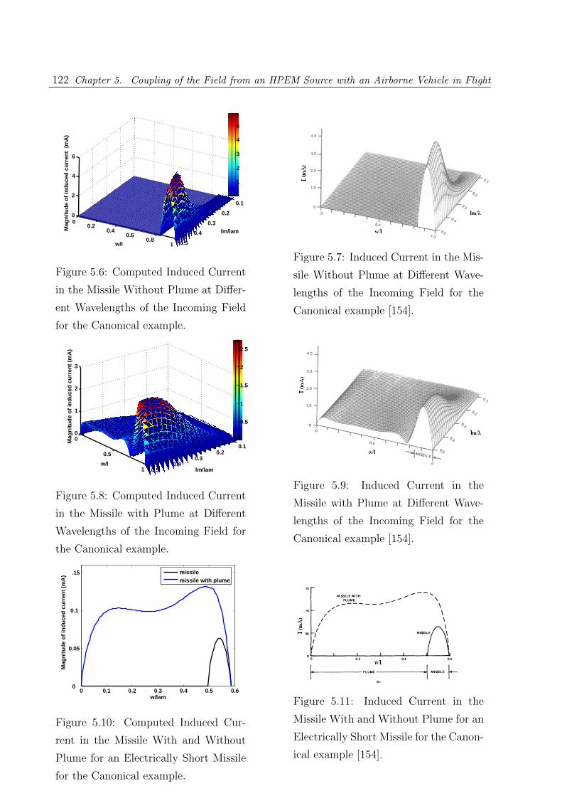
122 Chapter 5. Coupling of the Field from an HPEM Source with an Airborne Vehicle in Flight
0.1
0.2
0.3
0.4
0.5
00.2
0.40.6
0.81
0
2
4
6
lm/lam
w/l
Mag
nit
ud
e o
f in
du
ced
cu
rren
t (
mA
)
1
2
3
4
5
Figure 5.6: Computed Induced Current
in the Missile Without Plume at Differ-
ent Wavelengths of the Incoming Field
for the Canonical example.
Figure 5.7: Induced Current in the Mis-
sile Without Plume at Different Wave-
lengths of the Incoming Field for the
Canonical example [154].
0.10.2
0.30.4
0.5
0
0.5
1
0
1
2
3
lm/lamw/l
Mag
nit
ud
e o
f in
du
ced
cu
rren
t (m
A)
0.5
1
1.5
2
2.5
Figure 5.8: Computed Induced Current
in the Missile with Plume at Different
Wavelengths of the Incoming Field for
the Canonical example.
Figure 5.9: Induced Current in the
Missile with Plume at Different Wave-
lengths of the Incoming Field for the
Canonical example [154].
0 0.1 0.2 0.3 0.4 0.5 0.60
0.05
0.1
.15
w/lam
Mag
nit
ud
e o
f in
du
ced
cu
rren
t (m
A) missile
missile with plume
Figure 5.10: Computed Induced Cur-
rent in the Missile With and Without
Plume for an Electrically Short Missile
for the Canonical example.
Figure 5.11: Induced Current in the
Missile With and Without Plume for an
Electrically Short Missile for the Canon-
ical example [154].
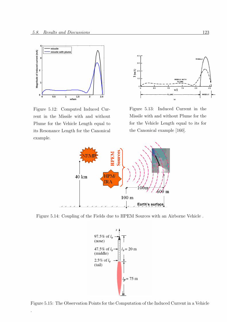
5.8. Results and Discussions 123
0 0.5 1 1.5 2 2.50
1
2
3
4
w/lam
Mag
nit
ud
e o
f in
du
ced
cu
rren
t (m
A) missile
missile with plume
Figure 5.12: Computed Induced Cur-
rent in the Missile with and without
Plume for the Vehicle Length equal to
its Resonance Length for the Canonical
example.
Figure 5.13: Induced Current in the
Missile with and without Plume for the
for the Vehicle Length equal to its for
the Canonical example [160].
Figure 5.14: Coupling of the Fields due to HPEM Sources with an Airborne Vehicle .
Figure 5.15: The Observation Points for the Computation of the Induced Current in a Vehicle
.

124 Chapter 5. Coupling of the Field from an HPEM Source with an Airborne Vehicle in Flight
These three points are shown in Fig. 5.15 for the vehicle. The induced voltage computed
is the difference between the voltages at the tail and the nose end of the vehicle. The induced
current and voltage is computed for three cases:
• The vehicle alone.
• Vehicle in the presence of a homogeneous plume
• Vehicle in the presence of an inhomogeneous plume
5.8.1 Coupling of NEMP with missile
The NEMP electric field is modelled according to the IEC 61000-2-9 as explained in the
chapter 2. These currents are plotted in Fig. 5.16 to Fig. 5.18. The induced current in
the vehicle without plume is extremely oscillatory with an exponential decay in the peak
magnitude with respect to time. But when an exhaust plume is present, the characteristics
of the current waveform changes to a smooth one that almost has the double exponential
behaviour of the interfering NEMP field. The magnitude of the current increases from 7 A
peak in the case when the plume is absent to 9 A in the presence of the plume at the nose of
the vehicle (Fig. 5.16). This current is 2 A at the tail end of the vehicle without the plume
and is 35 A with the plume present (Fig. 5.17). At the midpoint of the vehicle these values
are respectively 16 A and 27 A (Fig. 5.18). There is a large shoot up in the magnitude of
the current at the tail end in the presence of the conducting plume as compared to other
points, because of the conducting species in the plume that starts from the tail end of the
vehicle which adds to the contribution of the induced current and also, it acts as a channel
that routes the current to the vehicle. These currents can easily penetrate into the inner
circuitry of the vehicle causing more destruction.
The induced current over the entire vehicle and plume is plotted in Fig. 5.19 for all the
three cases explained in the previous section. The peak currents are 10 A, 70 A and 110 A
for a vehicle without plume, for a vehicle with an inhomogeneous plume and for a vehicle
with a homogeneous plume of conductivity 0.12 S/m as in the Fig. 5.19 respectively . The
induced current in the whole structure is highest for the third case, as the plume offers a
maximum conductivity that will cause higher currents to get coupled with the vehicle and
also with the plume. In the case of a non homogeneous plume there is a gradual distribution
of the conductivity, which peaks only at the tail end of the vehicle where the plume starts.
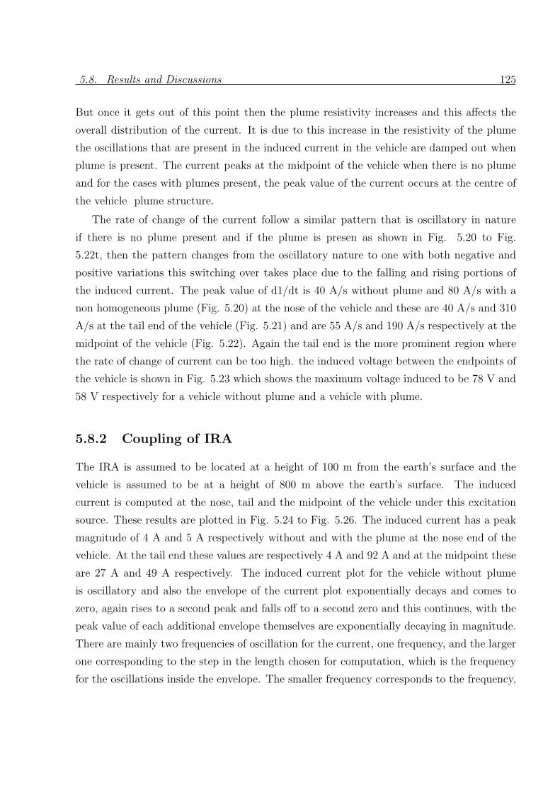
5.8. Results and Discussions 125
But once it gets out of this point then the plume resistivity increases and this affects the
overall distribution of the current. It is due to this increase in the resistivity of the plume
the oscillations that are present in the induced current in the vehicle are damped out when
plume is present. The current peaks at the midpoint of the vehicle when there is no plume
and for the cases with plumes present, the peak value of the current occurs at the centre of
the vehicle plume structure.
The rate of change of the current follow a similar pattern that is oscillatory in nature
if there is no plume present and if the plume is presen as shown in Fig. 5.20 to Fig.
5.22t, then the pattern changes from the oscillatory nature to one with both negative and
positive variations this switching over takes place due to the falling and rising portions of
the induced current. The peak value of d1/dt is 40 A/s without plume and 80 A/s with a
non homogeneous plume (Fig. 5.20) at the nose of the vehicle and these are 40 A/s and 310
A/s at the tail end of the vehicle (Fig. 5.21) and are 55 A/s and 190 A/s respectively at the
midpoint of the vehicle (Fig. 5.22). Again the tail end is the more prominent region where
the rate of change of current can be too high. the induced voltage between the endpoints of
the vehicle is shown in Fig. 5.23 which shows the maximum voltage induced to be 78 V and
58 V respectively for a vehicle without plume and a vehicle with plume.
5.8.2 Coupling of IRA
The IRA is assumed to be located at a height of 100 m from the earth’s surface and the
vehicle is assumed to be at a height of 800 m above the earth’s surface. The induced
current is computed at the nose, tail and the midpoint of the vehicle under this excitation
source. These results are plotted in Fig. 5.24 to Fig. 5.26. The induced current has a peak
magnitude of 4 A and 5 A respectively without and with the plume at the nose end of the
vehicle. At the tail end these values are respectively 4 A and 92 A and at the midpoint these
are 27 A and 49 A respectively. The induced current plot for the vehicle without plume
is oscillatory and also the envelope of the current plot exponentially decays and comes to
zero, again rises to a second peak and falls off to a second zero and this continues, with the
peak value of each additional envelope themselves are exponentially decaying in magnitude.
There are mainly two frequencies of oscillation for the current, one frequency, and the larger
one corresponding to the step in the length chosen for computation, which is the frequency
for the oscillations inside the envelope. The smaller frequency corresponds to the frequency,
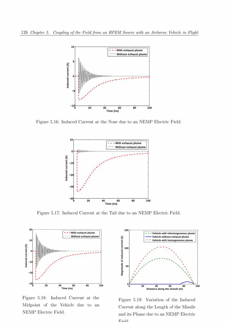
126 Chapter 5. Coupling of the Field from an HPEM Source with an Airborne Vehicle in Flight
0 20 40 60 80 100−10
−5
0
5
10
Time (ns)
Indu
ced
curr
ent (
A)
With exhaust plumeWithout exhaust plume
Figure 5.16: Induced Current at the Nose due to an NEMP Electric Field.
0 20 40 60 80 100−40
−30
−20
−10
0
10
Time (ns)
Indu
ced
curr
ent (
A)
With exhaust plumeWithout exhaust plume
Figure 5.17: Induced Current at the Tail due to an NEMP Electric Field.
0 20 40 60 80 100−30
−20
−10
0
10
20
Time (ns)
Indu
ced
curr
ent (
A)
With exhaust plumeWithout exhaust plume
Figure 5.18: Induced Current at the
Midpoint of the Vehicle due to an
NEMP Electric Field.
0 20 40 60 80 1000
50
100
150
Distance along the missile (m)
Mag
nit
ud
e o
f in
du
ced
cu
rren
t (A
)
Vehicle with inhomogeneous plumeVehicle without exhaust plumeVehicle with homogeneous plume
Figure 5.19: Variation of the Induced
Current along the Length of the Missile
and its Plume due to an NEMP Electric
Field.

5.8. Results and Discussions 127
0 20 40 60 80 100−100
−50
0
50
Time (ns)
di/d
t (A
/ns)
With exhaust plumeWithout exhaust plume
Figure 5.20: Derivative of Induced Current at the Nose due to an NEMP Electric Field.
0 20 40 60 80 100−350
−300
−250
−200
−150
−100
−50
0
50
100
Time (ns)
di/d
t (A
/ns)
With exhaust plumeWithout exhaust plume
Figure 5.21: Derivative of Induced Current at the Tail due to an NEMP Electric Field.
0 20 40 60 80 100−200
−150
−100
−50
0
50
100
Time (ns)
di/d
t (A
/ns)
With exhaust plumeWithout exhaust plume
Figure 5.22: Derivative of Induced Cur-
rent at the Midpoint of the Vehicle due
to an NEMP Electric Field.
0 20 40 60 80 100−80
−60
−40
−20
0
20
40
60
80
Time (ns)
Indu
ced
volta
ge (
V)
With exhaust plumeWithout exhaust plume
Figure 5.23: Induced Voltage Between
the Endpoints due to an NEMP Electric
Field.

128 Chapter 5. Coupling of the Field from an HPEM Source with an Airborne Vehicle in Flight
at which the envelopes themselves appear, which depends upon the time taken by each
travelling wave formed due to the induced current to reappear at the same point a second
time. The insertion of the non homogeneous plume causes the waveform to be smooth with
a single negative portion followed by a positive part, the negative portion being controlled
by the prepulse of the incident IRA field and the positive part by the impulse region of the
IRA field. There is an increase in the current magnitude if the plume is present, which is
mainly due to the presence of a finite conductivity exhaust gas that adds to the net current
contribution to the vehicle and also to the plume. Fig. 5.27 shows that the peak current is 20
A, 140 A and 255 A respectively for a vehicle with no plume present, with a non homogeneous
plume and for a homogeneous plume respectively. The reason for this response is the variable
conductivity of the plume in all the three cases. Also the homogeneous plume that has the
maximum conductivity causes more induced current and hence a higher interference to the
systems connected inside the vehicle. Hence the systems inside the vehicle should have
sufficient hardening to take care of this situation.
The rate of change of current also follows a similar pattern as current waveform when
there is no plume present, but in the presence of the plume the waveform is as shown in Fig.
5.28 to Fig. 5.30 for the nose, tail and the midpoint respectively. The zero crossings in the
waveform correspond to the points where induced current has minima and maxima points.
The peak magnitudes of di/dt are 34 A/ns and 45 A/ns for the missile in the absence and
presence of the plume respectively. These are respectively 34 A/ns and 720 A/ns for the
tail end of the vehicle and are respectively 200 A/ns and 450 A/ns for the midpoint of the
vehicle. A higher di/dt and current in the case of the IRA field adds to the damage potential
of this field.
The induced voltage between the endpoints of the vehicle is 140V and 160V respectively
for the vehicle without the plume and with the non homogeneous plume as in Fig. 5.31.
The waveform of the induced voltage is of the similar pattern as that of the current, and
the characteristics of the voltage is also identical. The induced voltage has a pattern similar
to that of the di/dt of the current, which indicates the reactive nature of the vehicle rather
than being resistive in nature. This nature imposes a higher induced voltage on account of
the rate of change of the magnetic field due to the currents in the vehicle structure.

5.8. Results and Discussions 129
2400 2450 2500 2550−10
−7.5
−5
−2.5
0
2.5
5
7.5
10
Time (ns)
Indu
ced
curr
ent (
A)
Vehicle without exhaust plumeVehicle with exhaust plume
Figure 5.24: Induced Current at the Nose due to an IRA Electric Field.
2400 2450 2500 2550−100
−75
−50
−25
0
25
50
75
100
Time (ns)
Indu
ced
curr
ent (
A)
Vehicle without exhaust plumeVehicle with exhaust plume
Figure 5.25: Induced Current at the Tail due to an IRA Electric Field.
2350 2400 2450 2500 2550−50
−40
−30
−20
−10
0
10
20
30
40
50
Time (ns)
Indu
ced
curr
ent (
A)
Vehicle without exhaust plumeVehicle with exhaust plume
Figure 5.26: Induced Current at the
Midpoint of the Vehicle due to an IRA
Electric Field.
0 20 40 60 800
50
100
150
200
250
300
350
400
Distance along the missile (m)
Mag
nit
ud
e o
f in
du
ced
cu
rren
t (A
)
Vehicle without plumeVehicle with inhomogeneous plumeVehicle with homogeneous plume
Figure 5.27: Variation of the Induced
Current along the Length of the Missile
and Plume due to an IRA Electric Field.

130 Chapter 5. Coupling of the Field from an HPEM Source with an Airborne Vehicle in Flight
2400 2450 2500 2550−50
−40
−30
−20
−10
0
10
20
30
40
50
Time (ns)
di/d
t (A
/ns)
Vehicle without exhaust plumeVehicle with exhaust plume
Figure 5.28: Derivative of Induced Current at the Nose due to an IRA Electric Field.
2400 2450 2500 2550−800
−600
−400
−200
0
200
400
600
800
Time (ns)
di/d
t (A
/ns)
Vehicle without exhaust plumeVehicle with exhaust plume
Figure 5.29: Derivative of Induced Current at the Tail due to an IRA Electric Field.
2350 2400 2450 2500 2550−500
−400
−300
−200
−100
0
100
200
300
400
500
Time (ns)
di/d
t (A
/ns)
Vehicle without exhaust plumeVehicle with exhaust plume
Figure 5.30: Derivative of Induced Cur-
rent at the Midpoint of the Vehicle due
to an IRA Electric Field.
2400 2450 2500 2550−200
−150
−100
−50
0
50
100
150
200
Time (ns)
Indu
ced
volta
ge (
V)
Vehicle without exhaust plumeVehicle with exhaust plume
Figure 5.31: Induced Voltage Between
the Endpoints due to an IRA Electric
Field.

5.8. Results and Discussions 131
5.8.3 Coupling of HPM
The high power microwave source is located at a height of 100 m from the earth’s surface and
the vehicle is located at a height of 800 m from the ground. The induced current is plotted
in Fig. 5.32, to Fig. 5.34 respectively for the nose, tail and the midpoint of the vehicle.
The maximum value of the induced current is 14 A and 20 A respectively for the vehicle
without plume and with plume. These currents are 14 A and 350 A at the tail end and are
100 A and 200 A at the midpoint. The waveform of the current without plume is oscillatory
with an exponential decay. The frequency of these oscillations is 1 GHz, the frequency of
the input field. If there is plume present, then the current has a waveform that is having a
shape similar to the interfering HPM field and with the frequency of GHz, but the repeated
oscillations in the case if plume is not there are absent as against the case when the plume is
present. In the case of NEMP and IRA, the oscillations in the induced current if the plume
is not there, are governed by the incremental step in the length taken, but with HPM it is
the characteristics of the field that governs the pattern of the current. The peak induced
current is 100 A, 500 A and 1400 A as shown in Fig. 5.35 for a vehicle without plume,
with a non-homogeneous plume and the vehicle with a homogeneous plume respectively. it
is reported in [100] that at a frequency of 2.29 GHz, loss tangent of the exhaust plume is
1, so the exhaust plume behaves as a good conductor for EM waves having frequency close
to 2.29 GHz. This effect is reflected in the current waveform since the HPM frequency is
1 GHz, where the plume has a tendency to be more conductive, that causes a rise in the
induced current magnitude.
The di/dt value for the vehicle without plume is 110 A/ns and is 145 A/ns with the plume
present at the nose of the vehicle. These values are respectively 110 A/ns and 2700 A/ns
at the tail end of the vehicle and are respectively 750 A/ns and 1500 A/ns at the midpoint
of the vehicle. these plots are shown in Fig. 5.36 to Fig. 5.38 The response of the induced
current follows a similar pattern as that of the current, because of its sinusoidal nature. The
di/dt values are the highest for the HPM as compared with the other HPEM sources. This
increases the destructive potential of the HPM sources to the vehicle. If there are apertures,
the HPM imposes further threat as it can easily get into the system and affect the circuits
inside.
The induced voltage in the vehicle between its endpoints is 480 V and 590V respectively
for a vehicle without the plume and a vehicle with plume as shown in Fig. 5.39. The
132 Chapter 5. Coupling of the Field from an HPEM Source with an Airborne Vehicle in Flight
characteristics of the voltage waveform are similar in pattern to that of the induced current
pattern.
5.9 Chapter summary
Coupling of the EM fields due to the HPEM sources with an airborne vehicle is computed.
The airborne vehicle is in flight and is assumed to be at a height of 800 m above the earths
surface. The HPEM sources are located at a height of 100 m except NEMP, which is a high
altitude burst. Based on the electric field along the surface of the vehicle structure, at all
points on the surface along its axis, a distributed excitation system can be arrived at. This
field forms the source for the generation of the currents and voltage along the vehicle and
the plume. Based on the computations the important inferences obtained are as follows:
• The species of the exhaust plume depends upon the chemical reactions taking place in
the combustion chamber of the nozzle.
• The presence of the alkali metals as impurity in the airborne vehicle propellant will
generate considerable ion particles such as Na+, Cl− in addition to e− in the plume
mixture during combustion which makes the plume electrically conducting. But it does
not influence the pressure, temperature and velocity of the plume.
• After the nozzle throat, the exhaust plume regains the supersonic speed, so the flow of
the exhaust plume is assumed as a compressible flow in the second region.
• The electrons have high collision frequency, high number density, high plasma frequency
and lower molecular mass and hence the highly mobile electrons dominate the heavy
ion particle in the computation of the electrical conductivity of the plume.
• The plume conductivity decreases marginally from the axis till a distance equal to the
nozzle radius but the peak value increases sharply towards the exit plane edge of the
nozzle radius. In the study, the peak value of the plume conductivity is found to be
0.12 S/m and it decreases to 0.02 S/m at an axial distance of 7.5 m from the exit plane
of the vehicle.
• At a frequency of 2.285 GHz, loss tangent of the exhaust plume is 1, so the exhaust
plume in the present study behaves as a good conductor.

5.9. Chapter summary 133
2389 2390 2391 2392 2393 2394 2395 2396 2397−20
−15
−10
−5
0
5
10
15
20
Time (ns)
Indu
ced
curr
ent (
A)
Vehicle without exhaust plumeVehicle with exhaust plume
Figure 5.32: Induced Current at the Nose due to an HPM Electric Field.
2389 2390 2391 2392 2393 2394 2395 2396 2397−400
−300
−200
−100
0
100
200
300
400
Time (ns)
Indu
ced
curr
ent (
A)
Vehicle without exhaust plumeVehicle with exhaust plume
Figure 5.33: Induced Current at the Tail due to an HPM Electric Field.
2355 2356 2357 2358 2359 2360 2361 2362 2363 2364−200
−150
−100
−50
0
50
100
150
200
Time (ns)
Indu
ced
curr
ent (
A)
Vehicle without exhaust plumeVehicle with exhaust plume
Figure 5.34: Induced Current at the
Midpoint of the Vehicle due to an HPM
Electric Field.
0 20 40 60 800
500
1000
1500
2000
Distance along the missile (m)
Mag
nit
ud
e o
f in
du
ced
cu
rren
t (
A)
Vehicle without plumeVehicle with inhomogeneous plumeVehicle with homogeneous plume
Figure 5.35: Variation of the Induced
Current along the Length of the Mis-
sile and Plume due to an HPM Electric
Field.
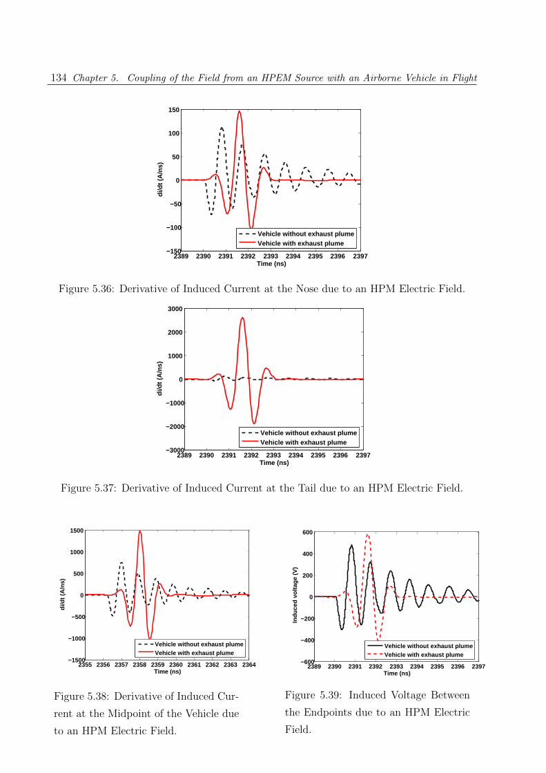
134 Chapter 5. Coupling of the Field from an HPEM Source with an Airborne Vehicle in Flight
2389 2390 2391 2392 2393 2394 2395 2396 2397−150
−100
−50
0
50
100
150
Time (ns)
di/d
t (A
/ns)
Vehicle without exhaust plumeVehicle with exhaust plume
Figure 5.36: Derivative of Induced Current at the Nose due to an HPM Electric Field.
2389 2390 2391 2392 2393 2394 2395 2396 2397−3000
−2000
−1000
0
1000
2000
3000
Time (ns)
di/d
t (A
/ns)
Vehicle without exhaust plumeVehicle with exhaust plume
Figure 5.37: Derivative of Induced Current at the Tail due to an HPM Electric Field.
2355 2356 2357 2358 2359 2360 2361 2362 2363 2364−1500
−1000
−500
0
500
1000
1500
Time (ns)
di/d
t (A
/ns)
Vehicle without exhaust plumeVehicle with exhaust plume
Figure 5.38: Derivative of Induced Cur-
rent at the Midpoint of the Vehicle due
to an HPM Electric Field.
2389 2390 2391 2392 2393 2394 2395 2396 2397−600
−400
−200
0
200
400
600
Time (ns)
Indu
ced
volta
ge (
V)
Vehicle without exhaust plumeVehicle with exhaust plume
Figure 5.39: Induced Voltage Between
the Endpoints due to an HPM Electric
Field.

5.9. Chapter summary 135
• The induced current depends upon the type of interference source, its characteristics,
whether the plume is present or not and the type of the plume.
• The HPM induces maximum current in the vehicle because of the fact that the plume
has a tendency to become more conductive at these frequencies. The IRA field and
the NEMP field follows HPM in its effect.
• The presence of the plume enhances the magnitude of the induced current. If the
plume is homogeneous then the current induced in it is more.
• The waveform of the induced current depends upon the incremental step in length if
the HPEM source is NEMP, depends upon the step in length and also the distance
travelled by the given pulse to reach the same point a second time, if the source of
interference is IRA and it depends upon the source characteristics alone if the source
is HPM.
Chapter 6
Conclusions
The HPEM sources are a major source of interference to electrical and electronic systems
that can possibly lead to a permanent damage or at least a temporary malfunctioning of the
equipments. Hence it is worthwhile to analyse the interaction of the radiated electric fields
from these sources with systems. In this thesis a buried cable and an airborne vehicle in
flight has been considered. The source characteristics are analysed from the data available
from the literature and the electric field is computed at any point from the HPEM sources,
based on their characteristic properties.
NEMP field at earth’s surface is modelled using the specifications given in the IEC
standard 61000-2-9 is used. The radiation pattern is calculated for the IRA using the aperture
integration using the aperture field which is shown in the chapter 2. The HPM field is
computed at the observation point using the non uniform aperture field. The electric field
at any point is a function of the type of the source and the characteristics of the source.
The maximum electric field occurs at the boresight. For an IRA, the shape of the radiation
pattern of the electric field is decided by the frequency, and also whether the observation
point is in the near or the far field with respect to the antenna.Polar plot of the radiation
pattern has no side lobes till the frequency is 50 MHz if the observation point is at 5m
but after wards it changes to irregular patterns with side lobes. Polar plot is having no
side lobes till 1500 MHz if the observation point changes to 100 m. This is decided by the
distance at which the far field commences for a given frequency. Beam width of the radiation
pattern decreases with an increase in the frequency for any observation point. The gain of the
antenna increases as square of the frequency with each increase in the frequency. The electric
field at the boresight of an IRA has a prepulse that lasts for 8 ns which accounts for the time
taken by the pulse to traverse the reflector diameter before it is felt at the given observation
136

137
point. For an HPM, the field has a centre frequency of 1 GHz, the centre frequency of the
waveguide field. The aperture field along the pyramidal horn antenna is mainly cosine in
nature with a maximum field at the centre of the horn cross section. The electric field at any
observation point is decided by the dimensions of the horn, the dimension of the reflector
antenna that finally radiates the field and also the characteristics of the waveguide field.
The electric field is computed in the air and in the soil for different characteristic proper-
ties of these media, by taking into account the Fresnel reflection and transmission coefficients
of the soil. The electric field propagation in any media is influenced by the properties of
the media, whether it is air or soil. As height increases the magnitude of the electric field
decreases for all types of sources and also the time before which the field waveform starts
is increased. The electric field in the soil is decided by the soil properties such as its con-
ductivity and permittivity. The soil is modelled in such a manner that its conductivity and
permittivity values are taken as a function of the frequency by giving due attention to the
high frequency behaviours of soils as the incident field has high frequency components. For
low soil conductivities the attenuation constant of the soil saturates soon, but it takes more
frequencies to saturate if the conductivity increases. For low soil conductivities, the conduc-
tion current to displacement current is low and it increases at higher conductivity. The skin
depth follows a reverse trend. A soil medium can be electromagnetically viewed as a four
component dielectric mixture consisting of soil particles, air voids, bound water, and free
water. When electric field is incident on the soil, it is polarized as a result of a wide variety
of processes, including polarization of electrons in the orbits around atoms, distortion of
molecules, reorientation of water molecules, accumulation of charge at interfaces, and elec-
trochemical reactions. Whatever is the HPEM source, an increase in the soil conductivity
results in more attenuation of the field. Also there is a significant loss of high frequency
components in the GHz range in the field due to selective absorption by the soil. This effect
cause the percentage attenuation to be maximum for HPM and minimum for NEMPand
IRA lying in between these two extremities. This is because HPM is mainly a narrow band
source with high frequency components in the GHz range, IRA has both GHz and MHz
frequencies, NEMP mainly having frequencies in the MHz range. Increase in permittivity of
the soil causes more attenuation of the electric field for all HPEM sources. This is due to the
relaxation mechanisms in the soil due to atomic- or molecular-scale resonances. As the depth
of burial of the cable increases, the field has to penetrate more through the soil medium,
hence suffering from increased opposition due to soil particles. Hence the field magnitude

138 Chapter 6. Conclusions
drops at higher depths. Soils in the city industrial areas have a higher field penetration and
soils in the moist wet lands provides the maximum attenuation.
This chapter deals with the computation of the induced current and voltage in a buried
cable. Two cables are considered - shielded cable and twisted pair cable. The results are
arrived at using the Enhanced Transmission Line model which is explained in the chapter.
The validation of the present model is done with the help of NEC V- 4 full wave analysis
and the results are found to be closely matching. The induced current is more for a shielded
cable than a twisted pair cable of the same configuration. The induced current magnitude
depends upon the type of the HPEM source, the depth of burial of the cable and the point
on the cable where the current/ voltage is computed. Current is maximum at the centre
of the cable for a matched termination and the voltage is the minimum at this point. The
percentage of the induced current in the inner conductor with respect to the shield current of
a shielded cable is the least for an HPM, then comes the IRA and finally NEMP. This is due
to the fact that higher frequencies are absorbed more by the shield of the cable. This affects
the induced voltage due to HPM the maximum and induced voltage due to NEMP the least
because of the presence of the lower frequency components in NEMP. Induced current in the
twisted pair cable depends upon the number of pairs of the cable and the pitching of the
cable for a given HPEM source. The percentage variation in the current between the induced
currents in the shielded and twisted pair cable is 67 for the NEMP, 40 for IRA and 37.5 for
the HPM. This is due to the fact that the smaller variations in the conductor dimensions are
negligible for frequencies in the GHz range. For the twisted pair cables, when the pitching
is equal to 4.5 times the diameter saturation limit of the induced current is reached. With
decrease in the pitching below this value, the current reduces proportionately. This can be
attributed to the reduction of the mutually induced currents when the twisting becomes
closer.
Coupling of the EM fields due to the HPEM sources with an airborne vehicle has also
been studied in this thesis. The airborne vehicle is in flight and is assumed to be at a height
of 800 m above the earths surface. The HPEM sources are located at a height of 100m
except NEMP, which is a high altitude burst. Based on the electric field along the surface
of the vehicle structure, at all points on the surface along its axis, a distributed excitation
system can be arrived at. This field forms the source for the generation of the currents and
voltage along the vehicle and the plume. The species of the exhaust plume depends upon the
chemical reactions taking place in the combustion chamber of the nozzle. The presence of
139
the alkali metals as impurity in the airborne vehicle propellant will generate considerable ion
particles such as Na+, Cl- in addition to e- in the plume mixture during combustion which
makes the plume electrically conducting. But it does not influence the pressure, temperature
and velocity of the plume. After the nozzle throat, the exhaust plume regains the supersonic
speed, so the flow of the exhaust plume is assumed as compressible flow in the second region.
The electrons have high collision frequency, high number density, high plasma frequency and
lower molecular mass and hence the highly mobile electrons dominate the heavy ion particle
in the computation of the electrical conductivity of the plume. The plume conductivity
decreases marginally from the axis till a distance equal to the nozzle radius but the peak
value increases sharply towards the exit plane edge of the nozzle radius. In the study, the
peak value of the plume conductivity is found to be 0.12 S/m and it decreases to 0.02 S/m
at an axial distance of 7.5 m from the exit plane of the vehicle. At a frequency of 2.285 GHz,
loss tangent of the exhaust plume is 1, so the exhaust plume in the present study behaves as
a good conductor. The induced current is computed using method of moments as it is found
to be more appropriate to an airborne vehicle in flight. The induced current depends upon
the type of interference source, its characteristics, whether the plume is present or not and
the type of the plume. The HPM induces maximum current in the vehicle because of the
fact that the plume has a tendency to become more conductive at these frequencies. The
IRA field and NEMP field follows HPM in its effect. The presence of the plume enhances the
magnitude of the induced current. If the plume is homogeneous, then the current induced in
it is more. The waveform of the induced current depends upon the incremental step in the
length if the HPEM source is NEMP, whereas it depends upon the incremental step in the
length and also the distance travelled by the given pulse to reach the same point a second
time, if the source of interference is IRA and it depends upon the source characteristics alone
if the source is HPM.
Scope of future work
The research work in this thesis can be extended further by including the following points:
• Experimental validation of the coupling of the HPEM sources with the buried cable.
• Experimental validation of the coupling with the airborne vehicle in the presence of
the exhaust plume due to HPEM sources.
• The coupling of transient electromagnetic fields with an airborne vehicle for different

140 Chapter 6. Conclusions
propellants used (such as liquid propellants instead of solid propellants as in the present
case).

References
[1] Daniel Mansson, Rajeev Thottappillil and Mats Backstrom, “Methodology for Classifying
Facilities with Respect to Intentional EMI”, IEEE Trans. on Electromag. Compat., Vol.
51, no. 1, pp. 46–52, Feb 2009.
[2] J. Delsing, , J. Ekman, J. Johansson, S. Sundberg, M. Backstrom and T. Nilsson, “Sus-
ceptibility of Sensor Networks to Intentional Electromagnetic Interference ”, Proc. 17th
Int. Zurich Symp. on Electromagn. Compat., pp. 172–175, Mar 2006.
[3] Daniel Mansson, Mats Backstrom and Rajeev Thottappillil, “Intentional EMI Against
Critical Infrastructures, a Discussion on Mitigation Philosophy”, In Proc. Asia-Pacific
Int. Symp. on Electromagn. Compat., pp. 134–137, Beijing, April 2010.
[4] Mats G. Backstrom, and Karl Gunnar Lovstrand , “Susceptibility of Electronic Systems
to High-Power Microwaves: Summary of Test Experience”, IEEE Trans. on Electromag.
Compat. , Vol. 46, no. 3, pp. 396–403, Aug 2006.
[5] Rajeev Thottappillil, Daniel Mansson and Mats Backstrom, “Response of Electrified
Railway Facilities to Intentional Electromagnetic Interference -Review of Research at
Uppsala University”, Asia-Pacific Symp. on Electromag. Compat., pp. 291–294, Singa-
pore, May 2008.
[6] Daniel Nitsch, Michael Camp, Frank Sabath, Jan Luiken ter Haseborg and Heyno Garbe,
“Susceptibility of Some Electronic Equipment to HPEM Threats”, IEEE Trans. on Elec-
tromagn. Compat., Vol. 46, no. 3, Aug 2004.
[7] William A. Radasky and Manuel. W. Wik, “Overview of the Threat of Intentional Elec-
tromagnetic Interference (IEMI)”, IEEE Int.Symp. on Electromag. Compat.,pp. 1024–
1027, May 2003.
141

142 References
[8] William A. Radasky , “The Threat of Intentional Electromagnetic Interference (IEMI) to
Wired and Wireless Systems”, Int. Zurich Symp. on Electromag. Compat., pp. 160–163,
Feb 2006.
[9] Yuri V. Parfenov, Leonid N. Zdoukhov, William A. Radasky, and Michel Ianoz, “Con-
ducted IEMI Threats for Commercial Buildings ”, IEEE Trans. on Electromagn. Com-
pat., Vol. 46, no. 3, pp. 404–411, Aug 2004.
[10] Manuel W. Wik, William A. Radasky, Robert L. Gardner ,“The Threat of Intentional
Electromagnetic Interference”, Asia-Pacific Conf. on Environ. Electromag., pp. 17–19,
Shanghai, May 2000.
[11] Van Keuren and J. Knighten, “Implications of the High-Power Microwave Weapon
Threat in Electronic System Design”, IEEE Int. Symp. On Electromag. Compat., pp.
370-371, Aug. 1991..
[12] William. A. Radasky,Edward Savage, “Intentional Electromagnetic Interference (IEMI)
and Its Impact on the U.S. Power Grid”, Tech. Rep.,Metatech Corporation, Meta- R-323,
Jan. 2010.
[13] William. A. Radasky, “Protection of Commercial Installations from the High-Frequency
Electromagnetic Threats of HEMP and IEMI using IEC standards”, Asia-Pacific Symp.
on Electromag. Compat., pp. 758–761, Beijing, May 2010
[14] D.V. Giri, and F. M. Tesche, “Classification of Intentional Electromagnetic Environ-
ments (IEME)”, IEEE Trans. on Electromagn. Compat., Vol. 46, no. 3, pp. 322–328,
Aug 2004.
[15] W. Radasky, “New Developments in Intentional Electromagnetic Interference (IEMI)
and High-Altitude Electomagnetic Pulse (HEMP) (Invited)”,Proc. Of URSI General As-
sembly, 2005.
[16] Manuel. W. Wik, and William. A. Radasky, “Intentional Electromagnetic Interference
(IEMI)-Background and Status of the Standardization Work in the International Elec-
trotechnical Commission (IEC)”,Proc. Of URSI General Assembly, 2002.

References 143
[17] William A. Radasky, Carl E. Baum, and Manuem W. Wik, “Introduction to the Special
Issue on High-Power Electromagnetics (HPEM) and Intentional Electromagnetic Inter-
ference (IEMI)”, IEEE Trans. on Electromagn. Compat., Vol. 46, no. 3, pp. 314–321,
Aug 2004.
[18] Manuel. W. Wik, and William. A. Radasky, “Development of High-Power Electromag-
netic (HPEM) Standards”, IEEE Trans. on Electromagn. Compat., Vol. 46, no. 3, pp.
439–445, Aug 2004.
[19] W. Radasky, “Progress in the Field of Intentional Electromagnetic Interference (IEMI)
Since the New Delhi General Assembly in 2005 ”,Proc. Of URSI General Assembly, 2008.
[20] Richard Hoad, William A. Radasky, “Progress in IEC SC 77C High-Power Electro-
magnetics Publications in 2009 ”, Asia-Pacific Symp. on Electromag. Compat., pp. 762–
765,Beijing, May 2010.
[21] EMP Engineering and Design Principles, Bell Telephone Laboratories Inc., Whippany,
NJ, 1975.
[22] R. N. Ghose, EMP Environment and System Hardness Design, Don White Consultants
Inc., Gainesville, Virgina, 1984.
[23] S. Glasstone and P.J. Dolan, The Effects of Nuclear Weapons, 3rd Edition, Castle House
Publication Ltd., 1980.
[24] I.N. Mindel,DNA EMP Awareness course Notes , 3rd Edition, I.I.T. Research Institute,
Chicago, Illionis, 1977.
[25] K.S.H. Lee (Ed.),EMP Interaction : Principles, Techniques and Reference Data , Hemi-
sphere Publishing Co., Washington D.C., 1986.
[26] E.J. Lerner, “Electromagnetic Pulses: Potential Crippler,”IEEE Spectrum, Vol. 18, No.
5, pp. 41–46, May 1981.
[27] J.B. Hays, “Protecting Communication Systems from EMP Effects of Nuclear Explo-
sions,”IEEE Spectrum, Vol. 1, No.5, pp. 115–122, May 1964.
[28] W.J. Broad, “Nuclear Pulse (III): Playing A Wild Card”, Science, Vol.212, No. 4500,
pp. 1248–1251, June 1981.

144 References
[29] E.J. Lerner, “EMPs and Nuclear Power,”IEEE Spectrum, Vol. 18, No. 6, pp. 48–49,
June 1981.
[30] L.W. Ricketts, J.E. Bridges and J.Mileta, EMP Radiation and Protective Techniques,
John Wiley and Sons Inc., New York, 1976.
[31] C.L.Longmire, “On the Electromagnetic Pulse Produced by Nuclear Explosions”, IEEE
Trans. on Electromag. Compat., Vol. EMC–20, No.1, pp. 3–13, Feb.1978.
[32] J.S. Forrest, “The Nuclear Electromagnetic Pulse,”IEE Review, Vol. 33, No. 7, pp.
443–444, July 1987.
[33] R.O. Lange, “Simulating the Electrical Effects of Nuclear Detonations,”IEEE Trans. on
Electromag. Compat., Vol. EMC–8, No.4, pp 197-209, Dec. 1966.
[34] C.L. Longmire, “On the Electromagnetic Pulse Produced by Nuclear Explosions”, IEEE
Trans. on Electromag. Compat., Vol. EMC–20, No.1, pp. 3–13, Feb.1978.
[35] C.E. Baum, “EMP Simulators for Various Types of Nuclear EMP Environments: An
interim categorization,”IEEE Trans. on Electromag. Compat., Vol. EMC-20, No. 1, pp.
35–53, Feb. 1978.
[36] Joy Thomas. M, “Developmental Studies of an Electromagnetic Pulse Simulator”, PhD
Thesis, Indian Institute of Science, Bangalore, India, 1993.
[37] J.C. Giles, “A Survey of Simulators of EMP outside the Source Region,”Proc. Int.
Conf. and Workshop on Electromagnetic Interference Compatibilty, Bangalore, India,
Sept. 1987.
[38] I.D. Smith and H. Aslin, “Pulsed Power for EMP Simulation,”IEEE Trans. on Electro-
mag. Compat., Vol. EMC - 20, No. 1, pp. 53–59, Feb. 1978.
[39] H.M. Shen, R.W.P. King and T.T. Wu, “The Exciting Mechanism of the Parallelplate
EMP Simulator,”IEEE Trans. on Electromag. Compat., Vol. EMC-29, No.1, pp. 32–39,
Feb. 1987.
[40] C.E. Baum, D.F. Higgins and D.V. Giri, “Pulser Test Results and Preliminary Esti-
mation of Transient Electric Field Waveforms in ATLAS 1,”ATLAS Memo No. 18, Oct.
1976.

References 145
[41] D.V. Giri, T.K. Liu,F.M. Tesche and R.W.P. King, “Parallel Transmission Line type of
EMP Simulator: A Systematic Review and Recommendations,”Sensor and Simulation
Note No. 261, April 1980.
[42] E.K. Miller, A. J. Poggio and G.J Burke, “An Integro Differential Equation Technique
for Time Domain Analysis of Thin Wire Structures”, J. Computational Physics, Vol.12,
pp.48, 1973.
[43] M. Jung, Th. H.G. G. Weise, U. Braunsberger and F. Sabath, “High Power Compact
UWB-Systems,”in Proc. Int. Conf. Pulsed Power Applications , Gelsenkirchen, Germany,
Mar. 2001.
[44] F. J. Agee and W. D. Prather, “Ultra-Wideband Transmitter Research,”IEEE Trans.
Plasma Sci., Vol. 26, June 1998.
[45] C. E. Baum, W. L. Baker, W. D. Prather, J. M. Lehr, J. P. OLoughlin, D. V. Giri, I.
D. Smith, R. Altes, J. Fockler, D. Mclemore, M. D. Abdalla, and M. C. Skipper, “JOLT:
A highly directive, very intensive, impulse-like Radiator”, Proc. IEEE, Vol. 92, pp, pp.
1096–1109, 2004.
[46] J. R. Mayes and W. J. Carey, ”The Marx Generator as an Ultra Wideband Source”
13th IEEE International Pulsed Power Conference, Las Vegas, NV, July 2001.
[47] Focia, R.J. Frost, C.A., A Compact, “Low Jitter, Fast Rise Time, Gas-Switched Pulse
Generator System with High Pulse Repetition Rate Capability”, 34 th IEEE Int. Conf.
on Plasma Science, pp. 363, June 2007.
[48] Verma R, Shyam A, Chaturvedi S, Kumar R, Lathi D, Sarkar P, Chaudhary V, Shukla
R, Debnath K, Sharma S, Sonara J, Shah K, Adhikary B, Jigna T, Piyush J., “Impulse
Electromagnetic Interference Generator”, Power Modulator Symposium, High-Voltage
Workshop. Conference Record of the Twenty-Sixth International, pp. 543–546, CA, 2004.
[49] Leland H. Bowen, Everett G. Farr, Dean I. Lawry, J. Scott Tyo ,“An Ultra-Compact
Impulse Radiating Antenna”, Sensor and Simulation Notes , Note 494, October 2004.
[50] Lanney M. Atchley, Everett G. Farr, J. Scott Tyo, Noel de la Merced, Larry L. Alt-
gilbers, “Development and Testing of a Parachute Deployable Impulse Radiating Antenna
”, Sensor and Simulation Notes, Note 465, March 2002

146 References
[51] W. D. Prather, C. E. Baum, F. J. Agee, J. P. OLaughlin, D. W. Scholfield, J. W. Burger,
J. Hull, J. S. H. Schoenberg and R. Copeland, “Ultrawide Band Sources and Antennas:
Present Technology, Future Challenges”Ultra-Wideband, Short Pulse Electromagnetics 3,
pp. 43–56, Plenum Press, NY, 1997.
[52] C. J. Buchenauer, J. S. Tyo and J. S. H. Schoenberg, “Antennas and Electric Field
Sensors for Ultra-Wideband Transient Time Domain Measurements: Applications and
Methods”Ultra- Wideband, Short Pulse Electromagnetics 3, pp. 405–422, Plenum Press,
New York, 1996.
[53] J. M. Lehr, M. D. Abdalla, F. Gruner, M. C. Skipper and W. D. Prather, “Development
of a Hermetically sealed, High-Energy Trigatron Switch for High Repetition Rate Ap-
plications,”12th IEEE International Pulse Power Conference, 1999, Monterey, CA, June
27–30, 1999, pp. 146–149.
[54] J. M. Lehr, M. D. Abdalla, J. W. Burger, J. M. Elizondo, J. Fockler, F. Gruner, M.
C. Skipper, I. D. Smith and W. D. Prather, “Design and Development of a 1 MV, Self
Break Switch for high Repetition Rate Operation,”12th IEEE International Pulse Power
Conference, 1999, Monterey, CA, June 27–30, 1999, pp. 1199–1202.
[55] William D. Prather, Carl E. Baum, Jane M. Lehr, Robert J. Torres, Tyrone C. Tran,
Jeffrey W. Burger, John A. Gaudet , “Recent Developments In Ultra-Wideband Sources
and Antennas ”, Ultra-Wideband, Short-Pulse Electromagnetics 5, Edited by P. D. Smith
and S. R. Cloude. Kluwer Academic/Plenum Publishers, 2002.
[56] W. Prather et al., “Ultra wideband sources and antennas,”UltraWideband Short Pulse
Electromagentics 4 . New York: Plenum, pp. 119–130, 1999.
[57] W. D. Prather, C. E. Baum, J. M. Lehr, J. P. OLoughlin, S. Tyo, J. S. H. Schoenberg,
R. J. Torres, T. C. Tran, D. W. Scholfield, J. W. Burger, and J. A. Gaudet, “Ultra-
Wideband Source Research”, IEEE 12th Intern. Pulse Power Conf., Vol. 1, Monterey,
CA., USA, pp. 185–189, 1999.
[58] J. S. H. Schoenberg, J. W. Burger, J. S. Tyo, M. D. Abdalla, M. C. Skipper, and
W. R. Buchwald, “Ultra-Wideband Source using Gallium Arsenide Photo Conductive
Semiconductor Switches,”IEEE Trans. Plasma Sci., Vol. 25, pp. 327–334, Apr. 1997.

References 147
[59] 59. C. E. Baum, E. G. Farr and D. V. Giri, “Impulse radiating antennas,”Ultra Wide-
band/ Short Pulse Electromagentics 2. New York: Plenum, pp. 139–147, 1993
[60] 60. E. G. Farr, Charles. A. Frost, “Development of a Reflector IRA and a Solid Lens
IRA, Part I: Design, Predictions and Construction,”Sensor and Simulation Note 396,
1996.
[61] D. V. Giri, H. Lackner, I. D. Smith, D. W. Morton, C. E. Baum, J. R. Marek, W.
D. Prather, and D. W. Scholfield, “Design, Fabrication, and Testing of a Paraboloidal
Reflector Antenna and Pulser System for Impulse like Waveforms,”IEEE Trans. Plasma
Sci., Vol. 25, pp. 318–326, Apr. 1997.
[62] E. G. Farr, C. E. Baum, and C. J. Buchenauer, “Impulse radiating antennas, Part
II,”Ultra-Wideband, Short Pulse Electromagnetics, H. L. Bertoni, L. Carin, and L. B.
Felsen, Eds. Plenum, New York 1993.
[63] D. V. Giri, J. M. Lehr, W. D. Prather, C. E. Baum and R. J. Torres, “Intermediate and
Far Fields of a Reflector Antenna Energized by a Hydrogen Spark-Gap Switched Pulser,
IEEE Trans. Plasma Sciences, Vol. 28, pp. 1631–1636, October 2000.
[64] C. E. Baum, E. G. Farr and D. V. Giri, “Review of Impulse-Radiating Anten-
nas,”chapter 16, pp 403–439, Review of Radio Science 1996-1999, Oxford University
Press.
[65] C. E. Baum, “Configurations of TEM Feed for an IRA,”Sensor and Simulation Note
327, 27 April 1991.
[66] C. E. Baum, “Variations on the Impulse Radiating Antenna Theme,”Sensor and Sim-
ulation Note 378, February 1995.
[67] E. G. Farr and C. E. Baum, “Feed-Point Lenses for Half-Reflector IRAs,”Sensor and
Simulation Note 385, November 1995.
[68] J. S. Tyo and J. S. H. Schoenberg, “Radiated Field Measurement from a 1-m Diameter
Half IRA,”Sensor and Simulation Note 471, February 1999.

148 References
[69] F. Sabath, D. Nitsch, M. Jung, Th. H. G. G. Weise, “Design and Setup of a short Pulse
Simulator for Susceptibility Investigations,”Sensor and Simulation Note 460, 1 October
2001.
[70] E. G. Farr and G. D. Sower, “Design Principles of Half-Impulse Radiating Antennas,
Sensor and Simulation Note 390, December 1995.
[71] D. V. Giri, High-Power Electromagnetic Radiators: Nonlethal Weapons and Other Ap-
plications, Harvard University Press, November 2004.
[72] W. Woo and D. V. Giri, “Directing HPM Radiation at Targets in Far Fields”, HPM
Research Note, Physics International Company, January 1988.
[73] D. V. Giri, “Preliminary Considerations for High Power Microwave Radiating Systems”,
Circuit and Electromagnetic System Design Note 40, December 28, 1990.
[74] Y.Rahmat-Samii, D.W.Duan, D.V.Giri, and L. F. Libelo, “Canonical Examples of Re-
flector antennas for High Power Microwave Applications,”IEEE Trans. Electromagn.
Compat., Vol. 34, No. 3, pp. 197–205, Aug. 1992.
[75] C. D. Taylor, D. V. Giri, High Power Microwave Systems and Effects , Taylor and
Francis, U. S. A, 1994.
[76] C. E. Baum, “Some Features of Waveguide/Horn Design ”Sensor and Simulation Note
314, 18 November 1988.
[77] E. Schamiloglu, “High Power Microwave Sources and Applications”, Microwave Sym-
posium Digest, IEEE MTT-S International, Vol.2, pp. 1001–1004, June 2004.
[78] Description of HEMP environment-radiated disturbance, IEC Standard 61000-2-9, 1996.
[79] C. A. Balanis, Antenna Theory Analysis and Design, John Wiley Sons Publishers, Inc.,
New York, 2005.
[80] 82. Oleg V. Mikheev, S. A. Podosenov, K .Y. Sakharov, A. A. Sokolov, Y. G. Svekis,
and V. A. Turkin, “New Method for Calculating Pulse Radiation from an Antenna with
a Reflector”, IEEE Trans. on Electromag. Compat., Vol. 39, no. 1, pp. 48–54, Feb 1997.

References 149
[81] C. E. Baum, “Radiation of Impulse-Like Transient Fields”, Sensor and Simulation Note
321, 25 November 1989.
[82] Jinliang He, Baoping Zhang, Rong Zeng, and Bo Zhang, “Experimental Studies of
Impulse Breakdown Delay Characteristics of Soil”, IEEE Trans. Power Delivery, Vol.
26, No. 3, pp. 1600-1607, July 2011.
[83] N. M. Nor, A. Haddad and H. Griffiths, “Determination of Threshold Electric Field,
Ec under High Impulse Currents”, IEEE Trans. Power Delivery, Vol. 20, pp. 2108–2113,
2005.
[84] Ovchinkin O.A. and Sugak, V.G., “The Influence of Soil Electric Properties upon the
Ground-Penetrating Radar (GPR) Signal Characteristics”, Telecommunications and Ra-
dio Engineering, Vol. 57, No’s 1011, pp. 101–109, 2002.
[85] Dobson, M.C., Ulaby, F.T., Hallikainen, M.T. and El-Rayes, M.A “Microwave Dielectric
Behaviour of Wet Soil. Part II: Dielectric Mixing Models”, IEEE Trans. on Geoscience
and Remote Sensing, Vol. 23, pp. 35–46, 1985
[86] Saarenketo, T., “Electrical Properties of Water in Clay and Silty Soils”, Journal of
Applied Geophysics, 40, pp. 73–88, 1998
[87] J.H.Scott, R. D. Carroll and D. R .Cunningham,”Dielectric Constant and Electrical
Conductivity of Moist Rock from Laboratory Measurements”, Sensor and Simulation
Note 116, Kirtland AFB, NM, August 1964.
[88] F. M. Tesche, “On the Modeling and Representation of a Lossy Earth for Transient
Electromagnetic Field Calculations”, Theoretical Note 367, July 9,2002.
[89] S.H. Zainud-Deen, M. E. Badr, E. M. Ali, K. H. Awadalla and H. A. Sharshar, “Effects
of Soil Physical Properties on Landmines Detection using Microstrip Antenna as a Sensor
”, Progress In Electromagnetics Research C, Vol. 7,pp.13–24, 2009
[90] Larisa Pozdnyakova, “Electrical Properties of Soils”, PhD Thesis, University of
Wyoming, Wyoming, 1999.
[91] Jackie E. Hipp, “Soil Electromagnetic Parameters as Functions of Frequency, Soil Den-
sity, and Soil Moisture”, Proc. Of IEEE, Vol. 62, No. 1, pp. 98–103 Jan 1974.

150 References
[92] Ronald. W. P. King, “The Transmission of Electromagnetic Waves and Pulses into the
Earth”, Journal of Applied Physics, Vol. 39, No.9, pp. 4444–4452, Aug 1968.
[93] E. Petrache, M. Paolone, F. Rachidi, C. A. Nucci, V. Rakov , M. Uman, D. Jordan,
K.Rambo, J. Jerauld, M. Nyffeler and J.Schoene, “Lightning induced currents in buried
coaxial cables: A frequency domain approach and its validation using rocket triggered
lightning”, J. Electrostat., Vol.65, No.5-6, pp. 322–328, May 2007.
[94] E. F. Vance, “Internal Voltages and Currents in Complex Cables”, Interaction Note 8,
June 1967.
[95] F. M. Tesche, M. Ianoz, T. Karlsson, EMC Analysis Methods and Computational Models,
Wiley – Interscience, New York, 1997.
[96] E. D. Sunde, Earth conduction effects in transmission systems, Dover, New York, 1968.
[97] Farhad Rachidi and Sergey V. Tkachenko, “Electromagnetic Field Interaction with
Transmission Lines from classical theory to HF Radiation Effects”, WIT Press, Boston,
2008.
[98] Clayborne D. Taylor, J. Philip Castillo, “On the Response of a Terminated Twisted-
Wire Cable Excited by a Plane-Wave Electromagnetic Field”, IEEE Trans. on Electro-
mag. Compat., Vol. EMC-22, No. 1, pp. 16–19, Feb 1980.
[99] D. J. Serafin , D. Dupouy, “Potential IEMI Threats Against Civilian Air Traffic”,Proc.
Of URSI General Assembly, 2005.
[100] Sisir Kumar Nayak, “Transient Lightning Electromagnetic Field Coupling with an
Airborne Vehicle in the Presence of its Conducting Exhaust Plume”, PhD Thesis Indian
Institute of Science, Bangalore, India, 2008.
[101] H. J. Christian, K. Crouch, B. Fisher, V. Mazur, R. A. Perala, and L. Ruhnke, “The
Atlas/Centaur lightning strike incident”, J. of Geophys. Res., Vol. 94, No. D11, pp.
13–169. 13 177, 1989.
[102] R. Godfrey, E. R. Mathews, and J. A. McDivit, “Analysis of Apollo 12 lightning
incident, Marshall Space Flight Center”, Tech. Rep. MSC-01540, NASA–TM–X–62894,
1970.

References 151
[103] J. A. Plumer, J. P. Moreau, and R. F. Hess, “The new aircraft lightning environment
and related test waveforms standard from SAE AE4L and EUROCAE WG31”, Proc.
International Conference on Lightning and Static Electricity , 1999–01–2395, Toulouse,
France, June 1999, pp. 383–391.
[104] M. A. Uman and V. A. Rakov, “The interaction of lightning with airborne vehicles”,
Progress in Aerospace Sciences, Vol. 39, pp. 61–81, 2003.
[105] T. R. Ferguson and R. H. Duncan, “Charged cylindrical tube”, J. of Appl. Phys., Vol.
32, No. 7, pp. 1385–1387, July 1961.
[106] W. R. Smythe, “Charged right circular cylinder”, J. of Appl. Phys., Vol. 27, No. 8, pp.
917–920, Aug 1956.
[107] W. R. Smythe, “Charged right circular cylinder”, J. of Appl. Phys., Vol. 33, No. 10,
pp. 2966–2967, Aug 1962.
[108] C. M. Butler, “Capacitance of a finite-length conducting cylindrical tube”, J. of Appl.
Phys., Vol. 51, No. 11, pp. 5607–5609, Nov 1980.
[109] L. Verolino, “Capacitance of a hollow cylinder”, Electrical Engineering, Springer-
Verlag, Vol. 78, No. 4, pp. 201–107, July 1995.
[110] E. A. Darrow and E. Lays, “Solid propellant rocket exhaust effects and methods of
attenuation”, Martin-Marietta Corporation, Denver, Colorado, Tech. Rep. NAS10-2300,
Martin–CR–65–93, Vol–I, Jan 1966.
[111] E. Lays and E. A. Darrow, “Solid propellant rocket exhaust effects and methods of
attenuation”, Martin-Marietta Corporation, Denver, Colorado, Tech. Rep. NAS10-2300,
Martin–CR–65–93, Vol–II, Jan 1966.
[112] E. Lays, “Design handbook for launch complexes from solid propellant exhaust”, Tech.
Rep. NAS10-2300, Martin–CR–66–11, March 1966.
[113] L. M. Hair and R. E. Somers, “Test data from small solid propellant rocket motor
plume measurements (FA-21)”, Tech. Rep. NASA-CR-150348, RTR–016–4, June 1976.

152 References
[114] D. E. Jensen and H. S. Pergament, “Effects of nonequilibrium chemistry on electrical
properties of solid propellant rocket exhaust plumes”, Combust. and Flame, Vol. 17, pp.
115–124, 1971.
[115] D. E. Jensen, “Competitive Reaction Kinetics in Seeded flames and Rocket Exhausts”,
Combust.and Flame, Vol. 18, pp. 217–223, 1972.
[116] D. E. Jensen and A. S.Wilson, “Prediction of rocket exhaust flame properties”, Com-
bust. and Flame, Vol. 25, pp. 43–55, 1975.
[117] D. E. Jensen and G. A. Jones, “Theoretical Aspects of Secondary Combustion in
Rockets Exhausts”, Combust. and Flame, Vol. 41, pp. 71–85, 1981.
[118] J. M. Cousins and D. E. Jensen, “On the Computation of Ionization Levels in Rocket
Exhaust Flames”, Combust. and Flame, Vol. 52, pp. 111–125, 1983.
[119] J. D. Nordgard and G. S. Smith, “A Plasma Model of Missile Exhaust plume”, Tech.
Rep. RADC–TR–77–144, 1977.
[120] J. D. Nordgard and G. S. Smith, “Electromagnetic Simulation of Missile Exhaust
Plumes”, IEEE Trans. on Electromagn. Compat. , Vol. 29, no. 2, pp. 157–168, May 1987.
[121] R. W. P. King, The Theory of Linear Antenna. Harvard University Press, Cambridge,
MA, 1956.
[122] G. Smith and K. Taylor, “Modelling of Two Phase Rocket Exhaust Plumes and other
Plume Prediction Developments”, 2000, [Online]. Available: www.cham.co.uk/Newvisitor
/cases/plume/plume.doc
[123] C. W. Dennis and P. Sutton, “Assessing Rocket Plume Damage to Launch Vehicles”,
41st AIAA/ASME/SAE/ASEE Joint Propulsion Conference and Exhibit , AIAA 2005–
4163,Tucson, Arizona, July 2005.
[124] S. K. Nayak and M. J. Thomas, “Electrical Characterization of Airborne Vehicle Ex-
haust Plume”, IEEE Trans. on Dielectric and Electrical Insulation,Vol.16, No. 2, April
2009.
References 153
[125] V. Cooray, M. Zitnik, M.Rahman, and Y. Liu, “Physical model of surge-current char-
acteristics of buried vertical rods in the presence of soil ionization”, J. of Electrostatics,
Vol. 60, pp. 193–202, 2004.
[126] M. Barrere, ( Rocket Propulsion), Elsevier, Van Nostrand, New York, 1960.
[127] G. P. Sutton and O. Biblarz, Rocket Propulsion Elements, 7th ed. JohnWiely and Sons,
New York, 2001.
[128] S. Gordon and B. J. McBride, “Computer program for calculation of complex chemical
equilibrium compositions and applications-I: Analysis”, NASA Lewis Research Center,
Cleveland, OH, Tech. Rep. NASA RP–1311, Oct 1994.
[129] B. J. McBride and S. Gordon, “Computer program for calculation of complex chemical
equilibrium compositions and applications II, Users manual and program descriptions”,.
NASA Lewis Research Center, Cleveland, OH, Tech. Rep. NASA RP–1311–P2, June
1996.
[130] E. Orberk, “Internal flow analysis of a technology demonstrator rocket motor with new
CFD code”, 34th AIAA/ASME/SAE/ASEE Joint Propulsion Conference and Exhibit,
AIAA–98–3967, Cleveland, OH, USA, 1998.
[131] S. V. Patankar, Numerical Heat Transfer and Fluid Flow, Taylor and Francis, 1980.
[132] H. K. Versteeg andW. Malalasekera, An Introduction to Computational Fluid Dynam-
ics: The Finite Volume Method, Pearson, Prentice Hall, 1995.
[133] J. O. Hinze, ( Turbulence, McGraw-Hill Publishing Co., New York, 1975.
[134] B. E. Launder and D. B. Spalding, Lectures in Mathematical Model of Turbulence,
Academic Press, London, England, 1972.
[135] V. Yakhot and S. A. Orszag, “Renormalization group analysis of turbulence: I. Basic
Theory”, J. of Scientific Computing, Vol. 1, No. 1, pp. 1–51, 1986.
[136] T. H. Shih, W. W. Liou, A. Shabbir, Z. Yang, and J. Zhu, “A New k- Eddy-Viscosity
Model for Higher Reynolds Number Turbulent Flows- Model, Development and Valida-
tion”, Computer Fluids, Vol. 24, No. 3, pp. 227–238, 1995.

154 References
[137] S. Sarkar and L. Balkrishnan, “Application of a Reynolds-Stress Turbulence Model to
the Compressible Shear Layer”, Tech. Rep. ICASE Report No. 90–18, NASA Contactor
Report 182002, NASA, Langley Research Center, Hampton, VA, Feb 1990.
[138] B. J. McBride, [Online], Available: www. galcit. caltech. edu/EDL/public/
thermo/nasadat
[139] B. J. McBride, M. J. Zehe, and S. Gordon, “NASA Glenn Coefficients for Calculating
Thermodynamic Properties of Individual Species”, Tech. Rep. NASA/TP–2002–211556,
Sep 2002.
[140] Q. Liu and P. Zhang, “Parameter identification of microwave attenuation of solid
rocket exhaust plumes”, 31st AIAA/ASME/SAE/ASEE Joint Propulsion Conference
and Exhibit, AIAA–95–2591, San Diego, CA, USA, July 1995.
[141] L. D. Smoot and D. L. Underwood, “Prediction of microwave attenuation characteris-
tics of rocket exhausts”, J. Spacecraft, Vol. 3, pp. 302–309, 1966.
[142] A. T. Adams, Electromagnetics for Engineers, Ronald Press, New York, 1972
[143] R. P. Feynman, R. B. Leighton, and M. Sands, The Feynman Lectures on Physics-Vol.
2, Narosa Publishing House, New Delhi, 1998.
[144] J. D. Kraus, Electromagnetics, Mc Graw-Hill, New York, 1991.
[145] R. C. Dorf, The Electrical Engineering Handbook, CRC Press, Boca Raton, FL, 1993,
pp. 935–947.
[146] R. F. Harrington, Field Computation by Moment Methods, The Macmillan Company,
New York, 1968.
[147] C. D. Taylor, “Electromagnetic scattering by thin inhomogeneous circular cylinders”,
Radio Science, Vol. 2, No. 7, pp. 729–738, July 1967.
[148] J. C. W. Harrison and E. A. Aronson, “On the Response of Missile with Exhaust
Trail of Tapered Conductivity to Plane Wave Electromagnetic Field”, IEEE Trans. on
Electromagn. Compat., Vol. 11, no. 2, pp. 40–50, May 1969.

References 155
[149] C. D. Taylor, C.W. H. Jr, and E. A. Aronson, “Resistive Receiving and Scattering
Antenna”, IEEE Trans. on Antenna and Propagation, Vol. 15, No. 3, pp. 371–376, May
1967.
[150] J. C. W. Harrison, “Missile Circumferential Current Density for Plane Wave Electro-
magnetic Field Illumination”, IEEE Trans. on Electromagn. Compat., Vol. 13, No. 2, pp.
35–40, May 1971.
[151] D. E. Merewether, “Transient Current Induced on a Metallic Body of Revolution by
an Electromagnetic Pulse”, IEEE Trans. on Electromagn. Compat., Vol. 13, No. 2, pp.
41–44, May 1971.
[152] D. E. Rosner, “Estimation of Electrical Conductivity at Rocket Nozzle Exit Sections”,
J. Amer. Rocket Soc., Vol. 32, pp. 1602–1605, Oct 1962.
[153] G. S. Smith, J. D. Nordgard,W. A. Holm, and H. L. Bassett, “Electromagnetic Simula-
tion of Missile Exhaust Plumes, Construction and Testing of a Physical Plume Simulator
and the Predicted Results of a Theoretical Thin Wire Rocket/Plume Model”, Tech. Rep.
RADC–TR– 81–8, 1981.
[154] G. S. Smith, J. D. Nordgard, and J. Edwards, “Alteration of the Surface Current on a
Missile by the Presence of an Exhaust Plume”, IEEE Trans. on Electromagn. Compat.,
Vol. 19, No. 4, pp. 383–394, May 1977.
[155] E. A. Aronson, C. D. Taylor, “Matrix Methods for Solving Antenna Problems”, IEEE
Trans. on Antennas and Propagation, pp. 696–697, Sep 1967.