
Beam Steering with a Nonlinear Optical Phased Array Antenna · 2−gold-phased array antenna and...
7
Beam Steering with a Nonlinear Optical Phased Array Antenna Sebastian Busschaert, Nikolaus Flö ry, Sotirios Papadopoulos, Markus Parzefall, Sebastian Heeg, and Lukas Novotny* Photonics Laboratory, ETH Zü rich, 8093 Zü rich, Switzerland * S Supporting Information ABSTRACT: Transition metal dichalcogenides (TMDCs) exhibit high second harmonic (SH) generation in the visible due to their noncentrosymmetric crystal structure in odd- layered form and direct bandgap transition when thinned down to a monolayer. In order to emit the SH radiation into a desired direction, one requires a means to control the phase of the in-plane nonlinear polarization. Here, we couple the SH response of a monolayer MoS 2 to an optical phased array antenna and demonstrate controllable steering of the nonlinear emission. By exploiting the intrinsic SH generation by the phased array antenna we achieve uniform emission efficiency into a broad angular range. Our work has relevance for novel optoelectronic applications, such as programmable optical interconnects and on-chip LIDAR. KEYWORDS: Nonlinear optics, second harmonic generation, TMDC, phased array antenna, beam steering, LIDAR, optical interconnects N onlinear optical effects play a vital role in integrated photonics as frequency mixing and electro-optic modulation are necessary components for optical multiplexing and optoelectronic logic gates. 1,2 However, due to the generally weak nonlinear material responses, accessing these effects requires high incident powers. This has led to an ongoing quest for materials with high intrinsic nonlinearities that can be incorporated into nanoscale devices. In addition, only noncentrosymmetric materials are capable of producing second order nonlinearities in the electric dipole approxima- tion. Unfortunately, common materials such as silicon or gold are centrosymmetric and noncentrosymmetric materials such as lithium niobate are difficult to process on nanometer length- scales. 3−5 Transition metal dichalcogenides (TMDCs) are a new class of materials that possess a strong nonlinear response and that can be structured with top-down nanofabrication techniques. These materials can be thinned down to monolayer form via mechanical exfoliation, which leads to the formation of a direct bandgap semiconductor. 6 Any odd number of layers of TMDCs forms a noncentrosymmetric crystal and has been shown to exhibit high second-order nonlinearities with reported values up to χ (2) ∼ 10 −7 m/V for the monolayer form. 7,8 Second harmonic (SH) generation has been studied in detail for TMDCs and an extraordinarily high response was observed when the emission was chosen to be close to the optical bandgap of the respective material. 9 Recently, several reports have studied the interaction between a TMDC monolayer and plasmonic particles and demonstrated an enhancement of the SH response. 10,11 The SH radiation of TMDCs and other material systems can also be controlled by plasmonic and dielectric metasurfaces that shape the phase profile of the incoming light. 12−16 For on-chip optoelectronic applications, it is desirable to steer the emission into desired directions and to have programmable control over the emission direction. As depicted conceptually in Figure 1, we demonstrate a MoS 2 −gold-phased array antenna and demonstrate beam steering of SH radiation. We utilize the symmetry properties of the array and exploit the interplay between SH generated by MoS 2 and the phased array itself to generate a beam steering efficiency that is uniform over a broad angular range. For the experimental realization, our nonlinear phased array antennas were produced by the following procedure: First, arrays of equally spaced gold nanorods were fabricated using electron-beam lithography. These arrays were then charac- terized by scanning electron microscopy (SEM) and by nonlinear spectroscopy. A monolayer of MoS 2 was then deposited on top of an array by using a dry transfer technique. 17,18 The deposited MoS 2 interacts with the local optical near fields of the antenna elements and gives rise to SH generation. Nonlinear measurements before and after transfer of the MoS 2 on the same array allows us to quantify the nonlinear signal contributions. Received: May 17, 2019 Revised: July 30, 2019 Published: August 19, 2019 Letter pubs.acs.org/NanoLett Cite This: Nano Lett. 2019, 19, 6097-6103 © 2019 American Chemical Society 6097 DOI: 10.1021/acs.nanolett.9b02029 Nano Lett. 2019, 19, 6097−6103 Downloaded via ETH ZURICH on September 20, 2019 at 05:38:46 (UTC). See https://pubs.acs.org/sharingguidelines for options on how to legitimately share published articles.
Transcript of Beam Steering with a Nonlinear Optical Phased Array Antenna · 2−gold-phased array antenna and...

Beam Steering with a Nonlinear Optical Phased Array AntennaSebastian Busschaert, Nikolaus Flory, Sotirios Papadopoulos, Markus Parzefall, Sebastian Heeg,and Lukas Novotny*
Photonics Laboratory, ETH Zurich, 8093 Zurich, Switzerland
*S Supporting Information
ABSTRACT: Transition metal dichalcogenides (TMDCs)exhibit high second harmonic (SH) generation in the visibledue to their noncentrosymmetric crystal structure in odd-layered form and direct bandgap transition when thinneddown to a monolayer. In order to emit the SH radiation into adesired direction, one requires a means to control the phase ofthe in-plane nonlinear polarization. Here, we couple the SHresponse of a monolayer MoS2 to an optical phased arrayantenna and demonstrate controllable steering of the nonlinearemission. By exploiting the intrinsic SH generation by thephased array antenna we achieve uniform emission efficiencyinto a broad angular range. Our work has relevance for noveloptoelectronic applications, such as programmable opticalinterconnects and on-chip LIDAR.
KEYWORDS: Nonlinear optics, second harmonic generation, TMDC, phased array antenna, beam steering, LIDAR,optical interconnects
Nonlinear optical effects play a vital role in integratedphotonics as frequency mixing and electro-optic
modulation are necessary components for optical multiplexingand optoelectronic logic gates.1,2 However, due to thegenerally weak nonlinear material responses, accessing theseeffects requires high incident powers. This has led to anongoing quest for materials with high intrinsic nonlinearitiesthat can be incorporated into nanoscale devices. In addition,only noncentrosymmetric materials are capable of producingsecond order nonlinearities in the electric dipole approxima-tion. Unfortunately, common materials such as silicon or goldare centrosymmetric and noncentrosymmetric materials suchas lithium niobate are difficult to process on nanometer length-scales.3−5
Transition metal dichalcogenides (TMDCs) are a new classof materials that possess a strong nonlinear response and thatcan be structured with top-down nanofabrication techniques.These materials can be thinned down to monolayer form viamechanical exfoliation, which leads to the formation of a directbandgap semiconductor.6 Any odd number of layers ofTMDCs forms a noncentrosymmetric crystal and has beenshown to exhibit high second-order nonlinearities withreported values up to χ(2) ∼ 10−7m/V for the monolayerform.7,8 Second harmonic (SH) generation has been studied indetail for TMDCs and an extraordinarily high response wasobserved when the emission was chosen to be close to theoptical bandgap of the respective material.9
Recently, several reports have studied the interactionbetween a TMDC monolayer and plasmonic particles anddemonstrated an enhancement of the SH response.10,11 The
SH radiation of TMDCs and other material systems can alsobe controlled by plasmonic and dielectric metasurfaces thatshape the phase profile of the incoming light.12−16 For on-chipoptoelectronic applications, it is desirable to steer the emissioninto desired directions and to have programmable control overthe emission direction.As depicted conceptually in Figure 1, we demonstrate a
MoS2−gold-phased array antenna and demonstrate beamsteering of SH radiation. We utilize the symmetry propertiesof the array and exploit the interplay between SH generated byMoS2 and the phased array itself to generate a beam steeringefficiency that is uniform over a broad angular range.For the experimental realization, our nonlinear phased array
antennas were produced by the following procedure: First,arrays of equally spaced gold nanorods were fabricated usingelectron-beam lithography. These arrays were then charac-terized by scanning electron microscopy (SEM) and bynonlinear spectroscopy. A monolayer of MoS2 was thendeposited on top of an array by using a dry transfertechnique.17,18 The deposited MoS2 interacts with the localoptical near fields of the antenna elements and gives rise to SHgeneration. Nonlinear measurements before and after transferof the MoS2 on the same array allows us to quantify thenonlinear signal contributions.
Received: May 17, 2019Revised: July 30, 2019Published: August 19, 2019
Letter
pubs.acs.org/NanoLettCite This: Nano Lett. 2019, 19, 6097−6103
© 2019 American Chemical Society 6097 DOI: 10.1021/acs.nanolett.9b02029Nano Lett. 2019, 19, 6097−6103
Dow
nloa
ded
via
ET
H Z
UR
ICH
on
Sept
embe
r 20
, 201
9 at
05:
38:4
6 (U
TC
).Se
e ht
tps:
//pub
s.ac
s.or
g/sh
arin
ggui
delin
es f
or o
ptio
ns o
n ho
w to
legi
timat
ely
shar
e pu
blis
hed
artic
les.
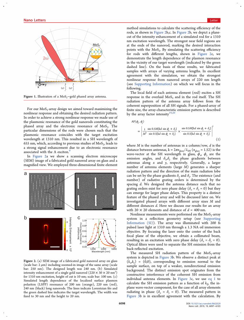
For our MoS2-array design we aimed toward maximizing thenonlinear response and obtaining the desired radiation pattern.In order to achieve a strong nonlinear response we made use ofthe plasmonic resonance of the gold nanorods constituting thephased array and the electronic resonance of MoS2. Theparticular dimensions of the rods were chosen such that theplasmonic resonance coincides with the target excitationwavelength at 1310 nm. This resulted in a SH wavelength of655 nm, which, according to previous studies of MoS2, leads toa strong signal enhancement due to an electronic resonanceassociated with the A exciton.9
In Figure 2a we show a scanning electron microscope(SEM) image of a fabricated gold nanorod array on glass and amagnified view. We employed three-dimensional finite element
method simulations to calculate the scattering efficiency of therods, as shown in Figure 2b,c. In Figure 2b, we depict a plane-cut of the intensity enhancement of a simulated rod for a 1310nm excitation wavelength. The strongest near field regions areat the ends of the nanorod, marking the desired interactionpoints with the MoS2. By simulating the scattering efficiencyfor rods with different lengths, shown in Figure 2c, wedemonstrate the length dependence of the plasmon resonancein the vicinity of our target wavelength (indicated by the greendashed line). On the basis of these results, we fabricatedsamples with arrays of varying antenna lengths. In excellentagreement with the simulation, we obtain the strongestnonlinear response from nanorod arrays of 220 nm length(see Supporting Information) on which we will focus in thefollowing.The local field of each antenna element (rod) excites a SH
response in the overlaid MoS2 and in the rod itself. The SHradiation pattern of the antenna array follows from thecoherent superposition of all SH signals. For a phased-array offinite size, the array-characteristic emission pattern is describedby the array factor intensity19,20
M
M d
d
M d
d
AF( , )
1 sin 0.5 k sin
sin 0.5 k sin
sin 0.5 k sin
sin 0.5 k sin
x y
x x
x x
y y
y y2
2
ϕ ϕ
ϕ δϕ δ
ϕ δ
ϕ δ=
[ + ][ + ]
×[ + ]
[ + ]
(1)
where M is the number of antennas in a column/row, d is thedistance between antennas, k = 2πnglass/λSH (nglass = 1.52) is thewave-vector at the SH wavelength in glass, ϕx, ϕy are theemission angles, and δx,δy the phase gradients betweenantennas along x and y, respectively. Generally, a largernumber of antenna elements (large M) generates a sharperradiation pattern and the direction of the main radiation lobecan be set by the phase gradients δx and δy. The existence (andnumber) of radiative grating orders is determined by thespacing d. We designed the antenna distance such that nograting orders exist for zero phase delay (δx = δy = 0) but theycan emerge for larger phase delays. This property is a distinctfeature of the phased array and will be discussed later on. Weinvestigated phased arrays with different array sizes M anddifferent distances d. Here we discuss our results for an arraywith 20 × 20 elements and distance of d = 400 nm.Nonlinear measurements were performed on the MoS2-array
system in a reflection geometry setup (see SupportingInformation (SI)). The array was illuminated with 200 fspulsed laser light at 1310 nm through a 1.3 NA oil immersionobjective. By focusing the laser onto the center of the backfocal plane of the objective, we obtain a collimated beam,resulting in an excitation with zero phase delay (δx = δy = 0).Optical filters were used to separate the SH emission from theback-reflected excitation.The measured SH radiation pattern of the MoS2-array
system is depicted in Figure 3b. We observe a distinct peak at(kx,ky) = (0,0), corresponding to emission normal to thesample surface, on top of a weaker, nondirectional emissionbackground. The distinct emission spot originates from theconstructive interference of the coherent SH emission fromindividual antenna elements. In Figure 3c, we use eq 1 tocalculate the SH emission pattern as a function of k∥, the in-plane wave-vector component, for the case of all array elementsradiating in phase (δx = δy = 0). The measured pattern inFigure 3b is in excellent agreement with the calculation. By
Figure 1. Illustration of a MoS2−gold phased array antenna.
Figure 2. (a) SEM image of a fabricated gold nanorod array on glass(scale bar: 2 μm) including zoomed-in image of the same array (scalebar: 250 nm). The designed length was 240 nm. (b) Simulatedintensity enhancement of a single gold nanorod (220 × 30 × 20 nm3)for 1310 nm excitation, height of cut is 10 nm; scale bar: 100 nm. (c)Simulated length dependence of the localized surface plasmonpolariton (LSPP) resonance of 200 nm (orange), 220 nm (red),240 nm (black) long nanorods. The lines indicate Lorentzian fits andthe green dashed line indicates the target wavelength. The width wasfixed to 30 nm and the height to 20 nm.
Nano Letters Letter
DOI: 10.1021/acs.nanolett.9b02029Nano Lett. 2019, 19, 6097−6103
6098
taking cross sections along kx for ky = 0 and transforming thespatial coordinate into an angular representation we plot inFigure 3d both the calculated and measured emission patternsas a polar plot. There is very good agreement between theoryand experiment. We also record the spectrum of the emissionfrom the MoS2-array system in a spectrometer (see Figure 3e),which shows the SH signal at 655 nm on top of a spectrally
broad background. The background is partially due to themultiphoton luminescence from gold21,22 (it also appears inmeasurements on bare gold arrays, see SI) and MoS2.
23,24
Because of its incoherent nature, the background is spectrallybroad and nondirectional, responsible for the weak backgroundsurrounding the sharp SH emission peak.
Figure 3. Nonlinear measurements of the MoS2-array system under normal incidence. (a) Illustration of the studied system. (b) Measured SHemission pattern of the coupled MoS2-array system. The rods are oriented along the y-direction. (c) Calculated SH emission pattern for 2D array
with M = 20. The black circles represent k k k kx y2 2
0= + = and k∥ = NA × k0, with NA = 1.3 being the numerical aperture of the objective. (d)
Polar plot of the calculated (line) and measured (points) SH pattern along the intensity maximum. The intensity is given in units of cts s−1 mW−2
μsr−1. (e) Spectrum of SH emission (excitation at 1310 nm).
Figure 4. Beam steering of SH emission by the phase delays along the x-direction (ϕx) and the y-direction (ϕy). The intensity of the measurementsis given in units of cts s−1 mW−2 μsr−1. (a) Calculated emission patterns for zero phase delay (blue) and nonzero phase delay (orange) betweenantenna elements. (b) Measured SH emission of a bare gold array (blue) and a MoS2-array (orange) for zero phase delay. (c,d) Same as (b) but fora phase delay along x yielding ϕx = 34° (c) and for a phase delay along y yielding ϕy = 34° (d).
Nano Letters Letter
DOI: 10.1021/acs.nanolett.9b02029Nano Lett. 2019, 19, 6097−6103
6099

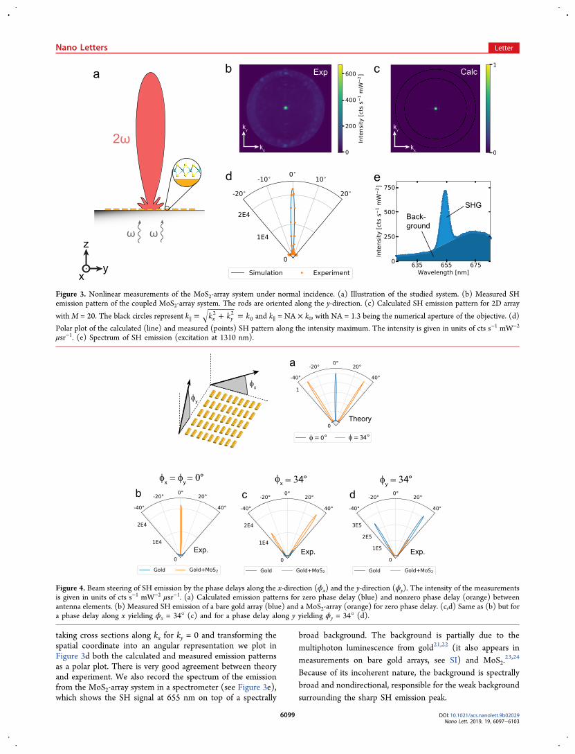
An important feature of a phased array antenna is the abilityto steer the emission and control the change of emissioncharacteristics, such as grating orders. Steering is achieved withthe phase gradients δx, δy in eq 1, which define a phase delaybetween antenna elements. In Figure 4a, we illustrate the SHemission of a two-dimensional array for two different phasegradients, which results in emission into angles ϕ = 0° and ϕ =34°, respectively. Experimentally, we achieve a nonzero phasedelay by laterally displacing the focus of the excitation beam inthe back focal plane of the 1.3 NA oil immersion objective.This leads to a tilted wavefront and hence to a linear phasegradient, as demonstrated in previous studies.25−27
In our experiments, we use MoS2 for nonlinear conversionand the gold-phased array to emit the SH radiation. It turnsout, however, that there is a finite SH contribution from thegold-phased array itself.28−30 In order to distinguish betweenthe two SH contributions, we investigate the phased arrayantenna before and after transfer of MoS2. Our experimentalresults show that for zero phase delay (δx = δy = 0) the SHcontribution from the gold array is negligible (Figure 4b). TheMoS2-array system exhibits the expected emission at 0°whereas no signal is observed for the bare gold array. Thesame observation holds for phase delays along the x-axis(Figure 4c), which corresponds to a tilt around the axis of ananorod. However, as shown in Figure 4d, the SH contributionfrom gold becomes more prominent for large phase delaysalong the y-axis, that is, tilts perpendicular to the nanorod axis.We will analyze this situation later on.Looking at the emission pattern shown in Figure 4c, we note
that there are two emission peaks, one at 34° (main emissionpeak) and the other at −34° (first grating order). Both of themare predicted by eq 1 and indicate the interaction between thegold nanorod array and the MoS2. We attribute the differencein signal strength between the two peaks to the irradiatedMoS2 not coupled to the array (in between antennas). In orderto quantify the interaction strength, we compare SHgeneration from the coupled MoS2-array system with SHgeneration from a bare MoS2 monolayer (see SI). We carry outthis comparison for δx = δy = 0, as the SH contribution fromthe gold array can be neglected in this case, cf. Figure 4b.Comparing the absolute intensities of the MoS2-array systemand the bare MoS2 only, we determine an enhancement of E =IMoS2−array/IMoS2 ≈ 1.6. This value denotes the area enhance-ment, that is, the enhancement averaged over many antennaelements. Note that the local signal enhancement at the polesof the nanorods is much larger (see Figure 2b).In Figure 4d, we apply a phase delay along the y-direction
which coincides with the nanorod axes. In contrast to theprevious case, we now observe a significant SH response fromthe bare gold array. We thus find that the SH signal emitted inthe (y,z) plane is dominated by the gold nanorods whereas theSH signal in the (x,z) plane originates from MoS2. This is afavorable finding as it allows us to emit SH radiation indifferent directions with similar efficiency.Let us analyze why the gold array generates significant SH
radiation only along one tilt axis. Although gold exhibits nobulk SH generation due to its crystal structure, symmetrybreaking at surfaces and edges can lead to a nonzero SHcontribution.31−34 The SH emission pattern of a singlenanorod is generated by the electric near fields at the endsof the rod (cf. Figure 2c). The resulting dipoles formed atopposite ends of the rod possess a phase difference of π, such
that their radiation destructively interferes in the farfield at anemission angle of 0°. The two out-of-phase dipoles give rise toa double-lobed SH emission pattern (Figure 5a). Thus, when
multiple nanorods are lined up in an array and radiate in phase,they destructively interfere at an emission angle of 0° (Figure5b). If the incoming beam is tilted such that the main emissionlobe is no longer normal to the surface, the destructiveinterference is lifted (Figure 5c). For this case SH generation isno longer dipole forbidden for observation angles in the (y,z)plane.In order to confirm the explanation described in Figure 5 we
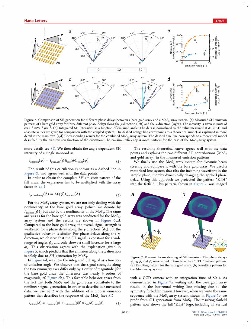
changed the phase delay along the two symmetry axes in smallincrements and tracked the SH intensity of the main emissionlobe. In Figure 6a, we show the behavior of the bare gold array,first for the y-direction (ϕy) and then the x-direction (ϕx). Forzero phase delay (δx = δy = 0), we do not observe anysignificant SH contribution, however as we increase the phasedelay along y the SH emission appears and increases withincreasing phase delay. For the x-direction, on the other hand,there seems to be only a small, negligible SH contribution(note the different scales in the plots). The integrated valuesfor several emission angles are compiled in Figure 6b andnormalized to the highest measured SH value. The valuesalong x are up to nearly 3 orders of magnitude smaller thanalong y and remain constant until the maximum applied phasedelay. In order to understand the increase of SH generationalong y, we consider two dipoles at opposite ends (asillustrated in Figure 5a) and calculate the radiation patternof a single nanorod as a function of solid angle Iquad,em(ϕ). Weaccount for the fact that the local excitation intensity is angle-dependent (due to the array) Iexc(ϕ). The same is true for thetransmission of the excitation through the sample Itrans(ϕ) (for
Figure 5. Symmetry considerations for SH generation from a baregold nanorod array. (a) Long axis view of single nanorod SH emission(only upper half space shown), indicated as red lobes. The emission isrotationally symmetric with respect to the y-axis. The black arrowsdenote electric dipoles. (b) Long axis view of a nanorod array undernormal incidence. Destructive interference cancels the SH emission.(c) Long axis view of a nanorod array under tilted incidence (tilt angleϕy).
Nano Letters Letter
DOI: 10.1021/acs.nanolett.9b02029Nano Lett. 2019, 19, 6097−6103
6100
more details see SI). We then obtain the angle-dependent SHintensity of a single nanorod as
I I I I( ) ( ) ( ) ( )antenna quad,em exc transϕ ϕ ϕ ϕ= (2)
The result of this calculation is shown as a dashed line inFigure 6b and agrees well with the data points.In order to obtain the complete SH emission pattern of the
full array, the expression has to be multiplied with the arrayfactor in eq 1
I I( ) AF( ) ( )phasedarray antennaϕ ϕ ϕ= (3)
For the MoS2-array system, we are not only dealing with thenonlinearity of the bare gold array (which we denote byIquad,em(ϕ)) but also by the nonlinearity of the MoS2. The sameanalysis as for the bare gold array was conducted for the MoS2-array system and the results are shown in Figure 6c,d.Compared to the bare gold array, the overall signal strength isweakened for a phase delay along the y-direction (ϕy) but thequalitative behavior is similar. For phase delays along the x-direction, we observe that the SH signal is constant for a widerange of angles ϕx and only shows a small increase for a largeϕx. This observation agrees with the explanation given inFigure 5, which predicts that the emission along the x directionis solely due to SH generation by MoS2.In Figure 6d, we show the integrated SH signal as a function
of emission angle. We observe that the signal strengths alongthe two symmetry axes differ only by 1 order of magnitude (forthe bare gold array the difference was nearly 3 orders ofmagnitude, cf. Figure 6b). This favorable behavior arises fromthe fact that both MoS2 and the gold array contribute to thenonlinear signal generation. In order to describe our measureddata, we use eq 2 with the addition of a dipolar emissionpattern that describes the response of the MoS2 (see SI)
I E E I I( ) ( ) ( ) ( ) ( )antenna quad,em dipole,em2
exc transϕ ϕ ϕ ϕ ϕ= | + | × (4)
The resulting theoretical curve agrees well with the datapoints and explains the two different SH contributions (MoS2and gold array) in the measured emission patterns.We finally use the MoS2-array system for dynamic beam
steering and compare it with the bare gold array. We used amotorized lens-system that tilts the incoming wavefront in thesample plane, thereby dynamically changing the applied phasedelay. Using this approach we projected the pattern “ETH”into the farfield. This pattern, shown in Figure 7, was imaged
with a CCD camera with an integration time of 50 s. Asdemonstrated in Figure 7a, writing with the bare gold arrayresults in the horizontal writing line missing due to thesymmetry forbidden region. However, when we write the samesequence with the MoS2-array system, shown in Figure 7b, weprofit from SH generation from MoS2. The resulting farfieldpattern now shows the full “ETH” logo, including all vertical
Figure 6. Comparison of SH generation for different phase delays between a bare gold array and a MoS2-array system. (a) Measured SH emissionpatterns of a bare gold array for three different phase delays along the y-direction (left) and the x-direction (right). The intensity is given in units ofcts s−1 mW−2 μsr−1. (b) Integrated SH intensities as a function of emission angle. The data is normalized to the value measured at ϕy = 34° andabsolute values are given for comparison with the coupled system. The dashed orange line corresponds to a theoretical model, as explained in moredetail in the main text. (c,d) Corresponding results for the combined MoS2-array system. The dashed blue line corresponds to a theoretical modeldescribed by the transmission function of the excitation. The emission efficiency is more uniform for the case of the MoS2-array system.
Figure 7. Dynamic beam steering of SH emission. The phase delaysalong ϕx and ϕy were varied in time to write a “ETH” far-field pattern.(a) Resulting pattern for the bare gold array. (b) Resulting pattern forthe MoS2-array system.
Nano Letters Letter
DOI: 10.1021/acs.nanolett.9b02029Nano Lett. 2019, 19, 6097−6103
6101

and horizontal lines. Thus, the combined MoS2-array systemallows us to steer SH radiation into arbitrary directions.In conclusion, we showed the nonlinear coupling of a
monolayer semiconductor, here MoS2, to an array of goldnanorods. The combined system functions as a phased arrayantenna that emits SH radiation into arbitrary directions. Beamsteering is accomplished by controlling the phase delaybetween antenna elements along the two main axes. Theemission efficiency is not only dictated by the array factor butalso by the emission pattern of a single antenna element. Thepresented results offer a new platform to study and understandthe coupling of second order nonlinear effects mediated byTMDCs and structured surfaces. Furthermore, nonlinearoptical phased array antennas can have applications fordynamical optical interconnects and on-chip LIDAR.Methods. Electrodynamic Simulations. Numerical simu-
lations were carried out with the RF module of COMSOLMultiphysics. A single gold rod with dimensions of 30 nmwidth, 20 nm height, and variable length was defined on top ofa glass substrate (n = 1.52), whereas the rod was surroundedby air (n = 1) in the other half space. For the dielectricfunction of gold we used measured values.35 The simulationswere carried out in two steps: First, the fields of the geometrywere simulated under plane wave illumination without rodsuch that the background field could be determined. The twohalf spaces were surrounded by perfectly matched layers toexclude back-reflection. In a a second step, the geometry wassimulated with a rod. The scattering efficiency of a single rodwas calculated by normalization with the cross-section of therod. For the final scattering efficiency comparison betweendifferent rods, we normalized the scattering efficiencies to thehighest simulated value for the 240 nm rod. Comparing theresonance condition of a single rod with the measuredresonance of the full array did not show any significantdeviations, which is due to the large separation betweenantenna elements (negligible near field interaction betweenantenna elements).Sample Fabrication. Phased array antennas were fabricated
on commercial glass coverslips. First, markers were patternedby means of UV lithography, evaporation of 5 nm titanium (Ti,0.05 nm/s) and 50 nm gold (Au, 0.2 nm/s) at a pressure of<10−7 mbar, and subsequent lift-off (acetone, ispropyl alcoholand deionized water). The antenna arrays consisting of Aunanorods were then defined by electron beam lithography(EBL) as single pixel lines (SPL, line-dose 1400 pAs/cm),followed by development and soft plasma cleaning (O2 plasma,70 W, 30 s). Twenty nanometers Au was deposited by electronbeam evaporation (0.1 nm/s) at a pressure of <10−7 mbar,followed by lift-off. For scanning electron microscopy, a samplefabricated with the same parameters was sputter-coated with1.5 nm Pt/Pd and then imaged using the in-lens detector(TLD) of a FEI Magellan 400 system.For the final structure including the monolayer MoS2, bulk
MoS2 crystal was exfoliated onto UV-ozone cleaned poly-dimethylsiloxane (PDMS). After observing a monolayer viaoptical contrast difference, the respective flake was stamped ontop of a suitable array with μm precision using a SUSSMicroTec mask aligner.Nonlinear Measurements. For the nonlinear measure-
ments, we used the IR output of an optical parametricoscillator (Coherent Mira-OPO) that provided 200 fs pulses ata repetition rate of 76 MHz. All experiments were conductedwith 1310 nm light. To exclude any pump contributions we
spectrally filtered the laser (Semrock BL 1110LP, ChromaHHQ940LP). The beam was sent into a 90°-periscopeconsisting of two motorized stages (PT1/M-Z8 by Thorlabs)and an attached lens (AC254−400-C-ML by Thorlabs), thatenabled us to focus the laser onto the back focal plane (BFP)of an oil immersion objective (1.3 NA Plan Fluor Nikon) andto laterally displace the beam. Focusing the laser onto the BFPleads to a large area illumination of the sample and lateraldisplacement of the beam gives rise to a wavefront tilt andhence a phase delay between antenna elements. With an initialbeam waist of 2 mm, the beam spot diameter in the sampleplane was roughly 10 μm. The average power before enteringthe periscope was determined to be 1.6 mW, resulting in anaverage power of 0.83 mW on the sample. The excitation peakintensity never exceeded 1 GW/cm2, which is below thedamage threshold for the gold nanorods. The incidentpolarization was chosen to be along the long axis of thenanorods.The excitation and emission wavelengths were separated by
a dichroic beamsplitter (DMSP950R by Thorlabs), furtherspectral selection was performed via optical filters (770SP,650/60BP for SH generation, 561SP for THG, all filters bySemrock) in front of the detectors. The emission was senteither to a spectrometer (Acton SP2300 with Pixis100 CCD)or an EMCCD (Acton Photon Max 512). Different lensarrangements were used for real space and Fourier spaceimaging.For calibration of the emission angles we used the first
concentric ring in the BFP (NA = 1 or ϕ = 41.14°) fornormalization. The error in determining the angle is ±1° (seeSupporting Information for more details).
■ ASSOCIATED CONTENT
*S Supporting InformationThe Supporting Information is available free of charge on theACS Publications website at DOI: 10.1021/acs.nano-lett.9b02029.
Nonlinear setup schematic; additional characterizationof bare gold arrays and MoS2-array system; explanationof polar plot representation; equations for the individualantenna emission patterns; measurement comparison forplasmonic enhancement calculation; measurements withnonresonant excitation; noise study of k-space measure-ments (PDF)
■ AUTHOR INFORMATION
ORCIDMarkus Parzefall: 0000-0003-2930-6698Sebastian Heeg: 0000-0002-6485-3083Lukas Novotny: 0000-0002-9970-8345NotesThe authors declare no competing financial interest.
■ ACKNOWLEDGMENTS
This work was financially supported by the Swiss NationalScience Foundation (Grant 200021_165841). S.H. acknowl-edges financial support by ETH Zurich Career Seed GrantSEED-16 17-1. The authors thank A. Jain for valuable inputduring sample fabrication and D. Windey for providing supportduring data analysis. Furthermore, the authors acknowledge
Nano Letters Letter
DOI: 10.1021/acs.nanolett.9b02029Nano Lett. 2019, 19, 6097−6103
6102

the use of the facilities of FIRST center of micro- andnanoscience and ScopeM at ETH Zurich.
■ REFERENCES(1) Luo, L.-W.; Ophir, N.; Chen, C. P.; Gabrielli, L. H.; Poitras, C.B.; Bergmen, K.; Lipson, M. Nat. Commun. 2014, 5, 3069EP.(2) Reis, C.; Chattopadhyay, T.; Andre, P.; Teixeira, A. Appl. Opt.2012, 51, 8693.(3) Boyd, R. W. Nonlinear Optics; Elsevier, 2008.(4) Sutherland, R. L. Handbook of Nonlinear Optics, 2nd ed.; OpticalEngineering; Marcel Dekker: New York, 2003; Vol. 82.(5) Siew, S. Y.; Cheung, E. J. H.; Liang, H.; Bettiol, A.; Toyoda, N.;Alshehri, B.; Dogheche, E.; Danner, A. J. Opt. Express 2018, 26, 4421.(6) Mak, K. F.; Lee, C.; Hone, J.; Shan, J.; Heinz, T. F. Phys. Rev.Lett. 2010, 105, 136805.(7) Kumar, N.; Najmaei, S.; Cui, Q.; Ceballos, F.; Ajayan, P. M.;Lou, J.; Zhao, H. Phys. Rev. B: Condens. Matter Mater. Phys. 2013, 87,161403.(8) Malard, L. M.; Alencar, T. V.; Barboza, A. P. M.; Mak, K. F.; dePaula, A. M. Phys. Rev. B: Condens. Matter Mater. Phys. 2013, 87,201401.(9) Zhao, M.; Ye, Z.; Suzuki, R.; Ye, Y.; Zhu, H.; Xiao, J.; Wang, Y.;Iwasa, Y.; Zhang, X. Light: Sci. Appl. 2016, 5, No. e16131.(10) Wang, Z.; Dong, Z.; Zhu, H.; Jin, L.; Chiu, M.-H.; Li, L.-J.; Xu,Q.-H.; Eda, G.; Maier, S. A.; Wee, A. T. S.; Qiu, C.-W.; Yang, J. K. W.ACS Nano 2018, 12, 1859.(11) Shi, J.; Liang, W.-Y.; Raja, S. S.; Sang, Y.; Zhang, X.-Q.; Chen,C.-A.; Wang, Y.; Yang, X.; Lee, Y.-H.; Ahn, H.; Gwo, S. Laser &Photonics Reviews 2018, 12, 1800188.(12) Chen, J.; Wang, K.; Long, H.; Han, X.; Hu, H.; Liu, W.; Wang,B.; Lu, P. Nano Lett. 2018, 18, 1344.(13) Hu, G.; Hong, X.; Wang, K.; Wu, J.; Xu, H.-X.; Zhao, W.; Liu,W.; Zhang, S.; Garcia-Vidal, F.; Wang, B.; Lu, P.; Qiu, C.-W. Nat.Photonics 2019, 13, 467.(14) Lochner, F. J. F.; Fedotova, A. N.; Liu, S.; Keeler, G. A.; Peake,G. M.; Saravi, S.; Shcherbakov, M. R.; Burger, S.; Fedyanin, A. A.;Brener, I.; Pertsch, T.; Setzpfand, F.; Staude, I. ACS Photonics 2018, 5,1786−1793.(15) Marino, G.; Gigli, C.; Rocco, D.; Lemaître, A.; Favero, I.; DeAngelis, C.; Leo, G. ACS Photonics 2019, 6, 1226−1231.(16) Vabishchevich, P. P.; Vaskin, A.; Addamane, S.; Liu, S.; Sharma,A. P.; Balakrishnan, G.; Reno, J. L.; Keeler, G. A.; Sinclair, M. B.;Staude, I.; Brener, I. Conference on Lasers and Electro-Optics,FM2C.3; 2019.(17) Castellanos-Gomez, A.; Buscema, M.; Molenaar, R.; Singh, V.;Janssen, L.; Van Der Zant, H. S.; Steele, G. A. 2D Mater. 2014, 1,011002.(18) Jain, A.; Bharadwaj, P.; Heeg, S.; Parzefall, M.; Taniguchi, T.;Watanabe, K.; Novotny, L. Nanotechnology 2018, 29, 265203.(19) Milligan, T. A. Modern Antenna Design; Wiley, 2005.(20) Balanis, C. A. Antenna theory: analysis and design; Wiley-Interscience, 2005.(21) Wang, T.; Halaney, D.; Ho, D.; Feldman, M. D.; Milner, T. E.Biomed. Opt. Express 2013, 4, 584.(22) Wang, S.; Xi, W.; Cai, F.; Zhao, X.; Xu, Z.; Qian, J.; He, S.Theranostics 2015, 5, 251.(23) Li, Y.; Dong, N.; Zhang, S.; Zhang, X.; Feng, Y.; Wang, K.;Zhang, L.; Wang, J. Laser & Photonics Reviews 2015, 9, 427.(24) Zhou, F.; Ji, W. Opt. Lett. 2017, 42, 3113.(25) Ghielmetti, G.; Aegerter, C. M. Opt. Express 2012, 20, 3744−3752.(26) Dregely, D.; Lindfors, K.; Lippitz, M.; Engheta, N.; Totzeck,M.; Giessen, H. Nat. Commun. 2014, 5, 4354SP.(27) Almeida, E.; Shalem, G.; Prior, Y. Nat. Commun. 2016, 7,10367SP.(28) McMahon, M. D.; Lopez, R.; Haglund, R. F.; Ray, E. A.;Bunton, P. H. Phys. Rev. B: Condens. Matter Mater. Phys. 2006, 73,041401.
(29) Hooper, D. C.; Kuppe, C.; Wang, D.; Wang, W.; Guan, J.;Odom, T. W.; Valev, V. K. Nano Lett. 2019, 19, 165.(30) Shams Mousavi, S. H.; Lemasters, R.; Wang, F.; Dorche, A. E.;Taheri, H.; Eftekhar, A. A.; Harutyunyan, H.; Adibi, A. Nanophotonics2019, 8, 607.(31) Bouhelier, A.; Beversluis, M.; Hartschuh, A.; Novotny, L. Phys.Rev. Lett. 2003, 90, 013903.(32) Bachelier, G.; Butet, J.; Russier-Antoine, I.; Jonin, C.; Benichou,E.; Brevet, P.-F. Phys. Rev. B: Condens. Matter Mater. Phys. 2010, 82,235403.(33) Reichenbach, P.; Eng, L. M.; Georgi, U.; Voit, B. J. Laser Appl.2012, 24, 042005.(34) Kauranen, M.; Zayats, A. V. Nat. Photonics 2012, 6, 737.(35) Johnson, P. B.; Christy, R. W. Phys. Rev. B 1972, 6, 4370.
Nano Letters Letter
DOI: 10.1021/acs.nanolett.9b02029Nano Lett. 2019, 19, 6097−6103
6103