
Be Project.pdf2
8
IEEE TRANSACTIONS ON INDUSTRIAL ELECTRONICS, VOL. 60, NO. 1, JANUARY 2013 3 Multilevel Current-Source Inverter With FPGA Control Miguel Pablo Aguirre, Member, IEEE, Laura Calvino, Student Member, IEEE, and María Inés Valla, Fellow, IEEE Abstract—In this paper, a multilevel current-source inverter (MCSI) topology is analyzed. The issue of constructing a novel modular single-rating inductor MCSI is explored, taking advan- tage of the features of field-programmable gate arrays (FPGA) for control and gate signal generation. The proposed topology is built with identical modules where all inductors carry the same amount of current, simplifying the construction and operation of industrial applications with higher efficiency. A new state- machine approach, which is easy to implement in an FPGA, and a proper implementation of the phase-shifted carrier sinusoidal pulse width modulation (PSC-SPWM) allow both current balance in all modules and effective switching-frequency minimization. The performance of the MSCI proposed is simulated with Matlab and is verified by constructing a prototype. Index Terms—Field-programmable gate array (FPGA), mul- tilevel current-source inverter (MCSI), phase-shifted carrier SPWM (PSC-SPWM). I. I NTRODUCTION R ECENT evolution of electronic switches, which are de- signed to rapidly turn on and off such as insulated gate bipolar transistors (IGBT), integrated gate-commutated thyris- tors (IGCT) [1], dual gate commutated thyristors (Dual GCT) [2], emitter turn-off thyristors (ETO) [3], and low-losses SiC devices [4], among others [5], has allowed the implementation of sinusoidal pulse with modulation (SPWM) techniques and multilevel schemes powered by a current source, ensuing low distortion and fast dynamic response in high-power applications [6]–[8]. Multilevel topologies present several advantages regarding total harmonic distortion and stress on inductors and switches [1], [6], [7]. Moreover, as shown in [9]–[11], multilevel current- source inverters (MCSIs) have usually more degrees of freedom than multilevel voltage-source inverters (MVSIs). The selected topology has as many degrees of freedom to impose different current levels in the three phases of the load as inductors acting as current sources. They are a smart choice to improve performance and efficiency in industrial applications [12], [13] Manuscript received December 29, 2010; revised April 21, 2011 and September 26, 2011; accepted November 21, 2011. Date of publication January 23, 2012; date of current version September 6, 2012. M. Aguirre is with the Instituto Tecnológico de Buenos Aires, 1106 Buenos Aires, Argentina, and also with the National University of La Plata, 1900 La Plata, Argentina (e-mail: [email protected]). L. Calvino was with Instituto Tecnológico de Buenos Aires, 1106 Buenos Aires, Argentina. She is now with the Department of Applied Physics, Eindhoven University of Technology, 5600 Eindhoven, The Netherlands (e-mail: [email protected]). M. I. Valla is with the National University of La Plata, 1900 La Plata, Argentina, and also with Consejo Nacional de Investigaciones Científicas y Técnicas, 1033 Buenos Aires, Argentina (e-mail: [email protected]). Digital Object Identifier 10.1109/TIE.2012.2185014 where high power or low voltage and high current are re- quired [9], [14], [15], such as induction motor drives [16], flexible alternating current transmission system (FACTS) [1], high-voltage direct-current (HVDC), and grid integration of renewable sources [17], [18]. CSI drives also show reliable overcurrent and short-circuit protection [13]. Several MCSI topologies have been developed and presented in the literature [18]–[23]. In this paper, a single-rating inductor MCSI is employed to feed a three-phase load. The converter consists of a number of identical modules, which determine the different current levels [20]. Each module uses two balance inductors and six power switches. All inductors of every module should carry the same amount of current. The current flowing through the inductors can be balanced, and switching frequency can be reduced by applying a state-machine modulation that properly uses redun- dant zero states [24]. Industrial assembles are easy to develop and to operate because all modules are identical [11]. The behavior of this converter is very different from the behavior of the traditional MVSI. Herein, each module carries a fraction of the load current, and there is no separation of modules or switches per phase as occur in an MVSI. In most MVSI, when a low voltage is delivered to the load, the outermost switches stop working, and the load current is only delivered by the switches connected close to the central point of the converter. This situation does not occur with the topology used for this MCSI. This converter with the proposed modulation always splits the output current among all the switches regardless of the modulation index (ma). The modulation and gate-drive control logic are implemented on a field-programmable gate array (FPGA), which is a power- ful cost-effective solution. It allows complex logical and control algorithms, fast speed, and multiple input/output pins, which becomes particularly attractive for multilevel-converter control [25], [26]. The behavior of the MCSI and the modulation technique has been previously presented in [11]. In this paper, the SPWM logic has been modified for better performance and FPGA implementation. A simple approach is presented showing that current balance can be provided by adapting a well-known SPWM strategy [11], [25], [27] while minimizing switching speed using a novel sequential machine design. Finally, a prototype is built to obtain experimental results that validate the proposal. In detail, this paper is organized as follows. The circuit is briefly described in Section II-A, followed by an analysis of the most important topics of the modulation method in Section II-B–D. Section III presents the evaluation of the 0278-0046/$31.00 © 2012 IEEE
-
Upload
hemanthbbc -
Category
Documents
-
view
17 -
download
0
Transcript of Be Project.pdf2

IEEE TRANSACTIONS ON INDUSTRIAL ELECTRONICS, VOL. 60, NO. 1, JANUARY 2013 3
Multilevel Current-Source InverterWith FPGA Control
Miguel Pablo Aguirre, Member, IEEE, Laura Calvino, Student Member, IEEE, and María Inés Valla, Fellow, IEEE
Abstract—In this paper, a multilevel current-source inverter(MCSI) topology is analyzed. The issue of constructing a novelmodular single-rating inductor MCSI is explored, taking advan-tage of the features of field-programmable gate arrays (FPGA)for control and gate signal generation. The proposed topology isbuilt with identical modules where all inductors carry the sameamount of current, simplifying the construction and operationof industrial applications with higher efficiency. A new state-machine approach, which is easy to implement in an FPGA, anda proper implementation of the phase-shifted carrier sinusoidalpulse width modulation (PSC-SPWM) allow both current balancein all modules and effective switching-frequency minimization.The performance of the MSCI proposed is simulated with Matlaband is verified by constructing a prototype.
Index Terms—Field-programmable gate array (FPGA), mul-tilevel current-source inverter (MCSI), phase-shifted carrierSPWM (PSC-SPWM).
I. INTRODUCTION
R ECENT evolution of electronic switches, which are de-signed to rapidly turn on and off such as insulated gate
bipolar transistors (IGBT), integrated gate-commutated thyris-tors (IGCT) [1], dual gate commutated thyristors (Dual GCT)[2], emitter turn-off thyristors (ETO) [3], and low-losses SiCdevices [4], among others [5], has allowed the implementationof sinusoidal pulse with modulation (SPWM) techniques andmultilevel schemes powered by a current source, ensuing lowdistortion and fast dynamic response in high-power applications[6]–[8].
Multilevel topologies present several advantages regardingtotal harmonic distortion and stress on inductors and switches[1], [6], [7]. Moreover, as shown in [9]–[11], multilevel current-source inverters (MCSIs) have usually more degrees of freedomthan multilevel voltage-source inverters (MVSIs). The selectedtopology has as many degrees of freedom to impose differentcurrent levels in the three phases of the load as inductorsacting as current sources. They are a smart choice to improveperformance and efficiency in industrial applications [12], [13]
Manuscript received December 29, 2010; revised April 21, 2011 andSeptember 26, 2011; accepted November 21, 2011. Date of publicationJanuary 23, 2012; date of current version September 6, 2012.
M. Aguirre is with the Instituto Tecnológico de Buenos Aires, 1106 BuenosAires, Argentina, and also with the National University of La Plata, 1900 LaPlata, Argentina (e-mail: [email protected]).
L. Calvino was with Instituto Tecnológico de Buenos Aires, 1106 BuenosAires, Argentina. She is now with the Department of Applied Physics,Eindhoven University of Technology, 5600 Eindhoven, The Netherlands(e-mail: [email protected]).
M. I. Valla is with the National University of La Plata, 1900 La Plata,Argentina, and also with Consejo Nacional de Investigaciones Científicas yTécnicas, 1033 Buenos Aires, Argentina (e-mail: [email protected]).
Digital Object Identifier 10.1109/TIE.2012.2185014
where high power or low voltage and high current are re-quired [9], [14], [15], such as induction motor drives [16],flexible alternating current transmission system (FACTS) [1],high-voltage direct-current (HVDC), and grid integration ofrenewable sources [17], [18]. CSI drives also show reliableovercurrent and short-circuit protection [13].
Several MCSI topologies have been developed and presentedin the literature [18]–[23].
In this paper, a single-rating inductor MCSI is employed tofeed a three-phase load. The converter consists of a number ofidentical modules, which determine the different current levels[20]. Each module uses two balance inductors and six powerswitches. All inductors of every module should carry the sameamount of current. The current flowing through the inductorscan be balanced, and switching frequency can be reduced byapplying a state-machine modulation that properly uses redun-dant zero states [24]. Industrial assembles are easy to developand to operate because all modules are identical [11]. Thebehavior of this converter is very different from the behaviorof the traditional MVSI. Herein, each module carries a fractionof the load current, and there is no separation of modules orswitches per phase as occur in an MVSI. In most MVSI, whena low voltage is delivered to the load, the outermost switchesstop working, and the load current is only delivered by theswitches connected close to the central point of the converter.This situation does not occur with the topology used for thisMCSI. This converter with the proposed modulation alwayssplits the output current among all the switches regardless ofthe modulation index (ma).
The modulation and gate-drive control logic are implementedon a field-programmable gate array (FPGA), which is a power-ful cost-effective solution. It allows complex logical and controlalgorithms, fast speed, and multiple input/output pins, whichbecomes particularly attractive for multilevel-converter control[25], [26].
The behavior of the MCSI and the modulation technique hasbeen previously presented in [11]. In this paper, the SPWMlogic has been modified for better performance and FPGAimplementation. A simple approach is presented showing thatcurrent balance can be provided by adapting a well-knownSPWM strategy [11], [25], [27] while minimizing switchingspeed using a novel sequential machine design. Finally, aprototype is built to obtain experimental results that validatethe proposal.
In detail, this paper is organized as follows. The circuitis briefly described in Section II-A, followed by an analysisof the most important topics of the modulation method inSection II-B–D. Section III presents the evaluation of the
0278-0046/$31.00 © 2012 IEEE

4 IEEE TRANSACTIONS ON INDUSTRIAL ELECTRONICS, VOL. 60, NO. 1, JANUARY 2013
Fig. 1. Basic MCSI scheme.
performance of the proposed system with simulation and ex-perimental results. A 3-kW prototype has been built, with allthe modulation and control logic embedded on a Xilinx Spartan3E FPGA. Finally, some conclusions are drawn in Section IV.
II. NOVEL CSI ARRANGEMENT
A. Switching Structure
The converter topology shown in Fig. 1 consists of multipleCSI subcircuits, sharing a common current source and con-nected in parallel with the load. Each group of six switchesand two inductors will be referred as a module. In this inverter,also known as the “single-rating inductor MCSI,” the sharinginductors split in equal shares the current from the main source.The inductors in series with the main source require a carefuldesign of the startup process of the main current source.
The modular structure is the main advantage of this MCSIconfiguration, where each identical module handles only afraction of the load current decreasing the overall switchinglosses [12]. The number of levels n in the output current canbe determined according to the number of modules m in
n = 2m + 1. (1)
In this paper, we consider m = 3 to obtain a load current withseven levels: I , 2/3I , 1/3I , 0, −1/3I , −2/3I , and −I .
The seven levels in the output current can be achieved by18 switches with bidirectional voltage blocking capability. Dep-ending on the power and frequency required by the application,the switches could be implemented by MOS transistors, IGBT,ETO, or IGCT, among others, with the addition of series diodes.
By turning on and off each switch, different load currentscan be obtained. An example of a valid switch combinationis shown in Fig. 2, and its corresponding switches states arepresented in Table I. Since each branch conducts a third ofthe supply current I and switches A1, B1, and C1 are on,then current into phase R equals I . The current in phase S isI/3 flowing from the load to the source through switch A5,and the current in phase T is 2/3I flowing toward the sourcethrough switches B6 and C6. It is worth noting that each outputcurrent level can be generated by more than one combination ofswitches. This redundancy gives more degrees of freedom thanthe MVSI to minimize the switching frequency of the converterand to balance the current of all the inductors.
Fig. 2. Current flow for a given switch configuration.
TABLE ISWITCHING COMBINATIONS FOR EXAMPLES IN FIG. 2
Fig. 3. SPWM modulation.
B. SPWM of One Module
SPWM is based on the comparison of a sinusoidal controlsignal with a triangular carrier. The switches on a single branchare turned on or off depending on whether the control signal isgreater or smaller than the carrier.
In SPWM for VSIs, the signals PR, PS , and PT [seeFig. 3(b)] are generated by the comparison of one triangularwith three sine waves [see Fig. 3(a)], and they directly drive theswitches of each leg of the VSI.
To generate the desired current level at the load while assur-ing current continuity in all the inductors, the driving signalsfor a CSI [see Fig. 3(c)] need more logic manipulation [28].The signals Pi are logically subtracted (unsigned) two at a timeto generate the firing signal of each switch (A1–A6), accordingto the logic diagram shown in Fig. 4. The combination of thevalid conditions of all the switches form a set of six active validstates that are shown in Table II.
A detailed analysis of the circuit topology, the modulationmethod, and simulations can be found in [11]. Space vectormodulation can be an alternative, although it requires somehigher computing efforts [29], [30].

AGUIRRE et al.: MCSI WITH FPGA CONTROL 5
Fig. 4. Gate-signal logic diagram.
TABLE IIDIRECT SPWM GATE SIGNALS
Fig. 5. Three different zero states.
C. Minimum Switching-Frequency Zero-State Selection
The signals generated in Fig. 3(c) cannot directly driveIGBT’s gates since they generate zero states by turning off allswitches (time z in Fig. 3), thus not allowing inductor’s currentcontinuity [28]. The zero states generated by the SPWM logicshould be recognized and replaced by adequate zero states, tak-ing advantage of the redundancy of the CSI topology [24], [31].Each module can generate optimal zero states in three differentways. Although closing all six switches of a module is thesimplest implementation at the expense of greater losses, themost efficient solution in terms of switching frequency consistson closing the two switches of a branch, as shown in Fig. 5.
A detailed analysis of the commutation signals (A1–A6) gen-erated with SPWM [see Fig. 3(c)] shows six main sequences,as shown in Fig. 6. Each sequence is a state of the sequentialmachine displayed in Fig. 6. The jump from one sequence tothe next is performed by detecting an active switching state thatdoes not belong to the sequence in progress.
Taking advantage of the calculation power of the FPGA, thelogic state machine is implemented to replace the zero statesgenerated by SPWM (all switches open) by the optimal zerocombination for each sequence that minimizes the number ofcommutations per period of each device.
Fig. 7 shows the gate signals of switch A1 as an example ofthe effect of the sequential machine on the commutation of thepower switches.
Fig. 6. Conmutation sequences and their corresponding states of the switches.
Fig. 7. Gate signal for switch A1. (a) Raw SPWM. (b) Sequential statemachine.
The asynchronous sequential state machine, as well as thecontrol logic, is implemented in Matlab Simulink. The controlscheme is then downloaded directly from Simulink to theXilinx FPGA after minimization and optimization for glitch-free operation. The FPGA program also includes an “allswitches closed” initial state for startup and safety purposes,not shown in Fig. 6 for simplicity.
D. Multilevel Operation: PSC-SPWM
To achieve multilevel output current in the load, multiplemodules are arranged. Seeking for a current balance over thesharing inductors, a phase-shifted carrier (PSC) SPWM wasadopted [27], [31]. The number of modules of the converterwill turn into the quantity of triangular carriers that are delayedan angle of
ϕk =2π
mk k = 1, 2, . . . ,m (2)
where m is the number of modules.In a similar way to MVSIs, the effective switching frequency
of the current at the load will be m · f , where f is the commuta-tion frequency of each module [32]. This allows faster dynamicresponse and easy filtering of the switching components. Theoutput waveform and spectrum of the proposed MCSI arecompared with a three-level CSI in Fig. 8, where all the power-device switch at the same frequency and the multilevel topologyshift the current spectrum to higher frequencies.
The complete modulation block diagram for the three-module seven-level converter is shown in Fig. 9.
6 IEEE TRANSACTIONS ON INDUSTRIAL ELECTRONICS, VOL. 60, NO. 1, JANUARY 2013
Fig. 8. Comparison of three-level CSI and the proposed MCSI. (a) Outputcurrent waveform. (b) Output current waveform detail. (c) Output currentspectra.
Fig. 9. Modulation diagram for the seven-level inverter.
Fig. 10. Schematic diagram of the experimental setup.
III. SIMULATION AND EXPERIMENTAL RESULTS
The proposed seven-level converter consists on three mod-ules. Each switch is implemented with an IGBT transistor anda series diode to allow bidirectional voltage blocking capabil-ities. A simple buck converter, with autonomous SPWM anda proportional–integral (PI) control, provides the energy to themain inductors. A 1.5-µF capacitor bank is used to filter theoutput current. Its capacitance is calculated to avoid the factthat the resonant frequency matches the harmonics generatedby the converter [29]. The load is composed of a three-phaseR-L series connection. Fig. 10 shows a schematic diagram ofthe experimental setup. The main parameters of the converterare summarized on Table III.
TABLE IIIINVERTER PARAMETERS
Fig. 11. (a) Inverter output current. (b) Load current.
A. Simulation
The performance of the proposed converter is simulatedwith Matlab Simulink. The converter arrangement is composedof three identical modules, each one built with six IGBTswith series diodes. The models used in the simulation matchthe characteristics of the transistors used in the prototype atan adequate level to give confidence on the validity of thesimulation. Moreover, the results have been validated with adetailed PSPICE simulation. The sequential state machine foreach module is implemented with Simulink’s state flow tool.
The output current of the simulated inverter is shown inFig. 11(a), where the seven levels (I, 2/3I, 1/3I, 0,−1/3I,−2/3I,−I) can be recognized. The output current is filteredby the small capacitor bank delivering a sinusoidal current tothe load [see Fig. 11(b)].
Fig. 12 shows the balanced operation of all sharing inductors.It is clear that each inductor carries an average value of one thirdof the main current even during the startup. A detail of one ofthese currents is shown in Fig. 12(b).
The behavior at different output current levels is shown inFig. 13, where amplitude modulation indexes of 0.95 and 0.2are considered. The load current loses levels, but the powercircuit redistributes the current among the switches of everymodule, maintaining the number of commutation per cycle.
This implies that the switching frequency at the load remainsm · f and that the average number of commutations per cycleof each switch remains constant for all load conditions. InFig. 13(b), the gate signals for switch 1 of each module showthat all the modules keep working even at low values of ma.
Changes in load resistance and/or inductance do not affectthe output current. Simulation results show that the currentbalance is not affected by changes in the load [11]. The loadcurrent can be as low as 10% of the nominal value, being limitedmainly by the bit resolution of the control in the FPGA.

AGUIRRE et al.: MCSI WITH FPGA CONTROL 7
Fig. 12. Inductor current balance. (a) Inductor current. (b) Sharing inductorcurrent detail.
Fig. 13. Behavior at ma = 0.95 and ma = 0.2. (a) Output current. (b) Gatesignals, switch 1 of each module.
B. Experimental Setup
The experimental setup has been designed as a small-scaleprototype of a high-current medium-voltage inverter [33]. Eachmodule has been planned with a modular structure. The hard-ware of the whole inverter has been carefully designed toavoid differences among the modules. Each switch has anindependent low power supply for isolated firing of its gate. Thelayout of the drive circuits has been constructed with physicaland electric symmetry so that the firing signals of the IGBThave no more than 10-ns difference in a module and amongmodules.
The six balance inductors have been built with the samematerials, proportions, and construction method. The air gapnecessary to allow the direct current that the inductors must
Fig. 14. Experimental setup.
Fig. 15. Experimental setup (one module overview).
handle has been carefully measured to minimize inductancedispersion. The converter cabinet is well ventilated to avoiddifferences in temperature. The layout of the PCB and thewiring have been cautiously implemented to guarantee symme-try among modules; to avoid resistance unbalances, capacitivecoupling, and stray capacitance; and to equally distribute thecurrents within each module.
The switches are implemented with an IRG4PC40UD IGBT,and the series diodes are RHRP1560. The main control,the state-machine zero selection, and the firing signals aregenerated with a Xilinx Spartan 3E FPGA. The FPGA isprogrammed directly from Matlab Simulink, allowing onlinesimulation and data collection. The prototype is shown inFigs. 14 and 15.
The steady-state operation as well as the startup and shut-down transients are shown in Fig. 16. The switch voltage isset by the load impedance. As shown in Fig. 16, no highvoltage spikes are generated; therefore, switch safety is notcompromised even under inductive load conditions.
8 IEEE TRANSACTIONS ON INDUSTRIAL ELECTRONICS, VOL. 60, NO. 1, JANUARY 2013
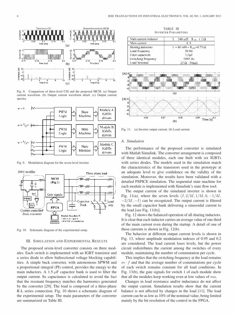
Fig. 16. Startup and shutdown transients. Load current and switch voltage.
Fig. 17. Startup and shutdown transients showing current balance.
This is due to the careful design of the wiring layout andPCBs, the overlapping of conduction times of the IGBT, andthe coupling capacitors [8]. Fig. 16 also shows that no volt-age spikes or current distortion is generated during startup orshutdown.
The soft start of the main-current PI control sets the risetime and dynamic characteristics of the output during startup,avoiding overvoltages in the current sharing inductors. Energystored in the main current-source inductors establishes theshutdown time. A complete cycle (startup, steady state, andshutdown) for the main current and two of the six sharinginductor currents is shown in Fig. 17. The main current, whichis regulated by a standard PI control, shows a small ripplecaused by the buck-converter switching frequency. The sharinginductor currents show a characteristic ripple waveform causedby the commutation of the switches of the whole converter. Thewaveforms of the experimental currents match the simulatedcurrents shown in Fig. 12. To warrant the safe operation thatany industrial application requires, a supervisory control systemmust be added to grant current balance, dealing with imbalancesin components, and unexpected disturbances. However, such acomplex control system is not necessary (neither desired) in aresearch prototype since it would mask the natural behavior ofthe converter.
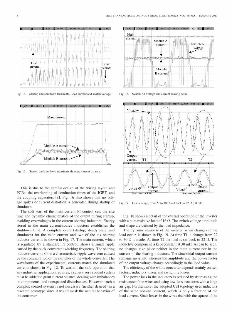
Fig. 18. Switch A1 voltage and current sharing detail.
Fig. 19. Load change, from 22 to 30 Ω and back to 22 Ω (30 mH).
Fig. 18 shows a detail of the overall operation of the inverterwith a pure resistive load of 16 Ω. The switch voltage amplitudeand shape are defined by the load impedance.
The dynamic response of the inverter, when changes in theload occur, is shown in Fig. 19. At time T1, a change from 22to 30 Ω is made. At time T2 the load is set back to 22 Ω. Theinductive component is kept constant at 30 mH. As can be seen,no changes take place neither in the main current nor in thecurrent of the sharing inductors. The sinusoidal output currentremains invariant, whereas the amplitude and the power factorof the output voltage change accordingly to the load value.
The efficiency of the whole converter depends mainly on twofactors: inductors losses and switching losses.
The power loss in the inductors is reduced by decreasing theresistance of the wires and using low-loss iron cores with a largeair gap. Furthermore, the adopted CSI topology uses inductorsof the same nominal current, which is only a fraction of theload current. Since losses in the wires rise with the square of the

AGUIRRE et al.: MCSI WITH FPGA CONTROL 9
Fig. 20. Reduced switching losses due to current overlapping.
current, keeping each inductor current low is a great advantageof this topology.
The total power loss in the prototype’s inductors at maximumload is about 2.5% of the output power.
The medium-power IGBTs used in the prototype typicallytake a very short time to turn on (about 150 ns) and a long timeto turn off (about 1 µs). The larger turn-off time is caused bythe recombination time of electrical charges in the bipolar partof the device once the MOS part has been shut down.
This overlapping allows a sort of soft switching of the currentof two adjacent switches in a module. An example of a commu-tation cycle is shown in Fig. 20. At the beginning, transistorT1 is conducting (ON), and transistor T2 is open (OFF). Whenthe commutation initiates, first, T2 turns on with zero current,and later, T1 turns off. Since T2 is already on when T1 turnsoff, there is a free path for the current of transistor T1 throughT2. The circuit layout is carefully designed to avoid strayinductances between the current paths of the transistors of eachmodule, helping to reduce the switching losses. An additionalSPWM scheme for natural soft commutation to increase theoverall efficiency can be found in [34].
The diodes in series with the IGBT still need to block the re-verse voltage present at the load, thus losing some power at turnoff. Considering a conservative analysis [35], the total loss dueto switching action is reduced to less than 1% of the load power.
IV. CONCLUSION
A novel modular single-rating inductor MCSI topology hasbeen analyzed in this paper. The behavior of a seven-levelthree-module arrangement was simulated, showing outstandingconditions of load regulation, linearity, and dynamic response.An experimental prototype was designed and built. The per-formance of the constructed prototype strongly matches thesimulated behavior due to a comprehensive construction of thesimulation model and a careful design of the PCBs and layout.
As a result of circuit topology and PSC-SPWM utilization,current balance was achieved in both main and sharing in-ductors, even under load and operating point changes. Theswitching frequency was drastically reduced with a new state-machine approach, taking the advantage of the three differentzero-states of the topology.
The topology adopted allows operation with high efficiencyby reducing the current through the inductors and the losses inthe switches.
The dynamic response of the output current is satisfactory,both the steady-state and transient behaviors show no voltagespikes or current unbalances, and low-frequency current har-monics are reduced according to the structure implemented andthe advanced switching method used; thus, the prototype isfully functional.
REFERENCES
[1] H. Bilgin and M. Ermis, “Design and implementation of a current-sourceconverter for use in industry applications of D-STATCOM,” IEEE Trans.Power Electron., vol. 25, no. 8, pp. 1943–1957, Aug. 2010.
[2] T. Butschen, J. Zimmermann, and R. W. De Doncker, “Development of adual GCT,” in Proc. IPEC, Jun. 21–24, 2010, pp. 1934–1940.
[3] Y. Li, A. Q. Huang, and K. Motto, “Series and parallel operation of theemitter turn-off (ETO) thyristor,” IEEE Trans. Ind. Appl., vol. 38, no. 3,pp. 706–712, May/Jun. 2002.
[4] J. Biela, M. Schweizer, S. Waffler, and J. W. Kolar, “SiC versusSi–Evaluation of potentials for performance improvement of inverter andDC–DC converter systems by SiC power semiconductors,” IEEE Trans.Ind. Electron., vol. 58, no. 7, pp. 2872–2882, Jul. 2011.
[5] B. Zhang, A. Q. Huang, B. Chen, S. Atcitty, and M. Ingram, “SPETO: Asuperior power switch for high power, high frequency, low cost convert-ers,” in Conf. Rec. 39th IEEE IAS Annu. Meeting, Oct. 3–7, 2004, vol. 3,pp. 1940–1946.
[6] B. P. McGrath and D. G. Holmes, “Natural current balancing of multicellcurrent source converters,” IEEE Trans. Power Electron., vol. 23, no. 3,pp. 1239–1246, May 2008.
[7] J. Rodriguez, L. G. Franquelo, S. Kouro, J. I. Leon, R. C. Portillo,M. A. M. Prats, and M. A. Perez, “Multilevel converters: An enablingtechnology for high-power applications,” Proc. IEEE, vol. 97, no. 11,pp. 1786–1817, Nov. 2009.
[8] M. P. Kazmierkowski, L. G. Franquelo, J. Rodriguez, M. A. Perez, andJ. I. Leon, “High-performance motor drives,” IEEE Ind. Electron. Mag.,vol. 5, no. 3, pp. 6–26, Sep. 2011.
[9] S. Kouro, M. Malinowski, K. Gopakumar, J. Pou, L. G. Franquelo, B. Wu,J. Rodriguez, M. A. Perez, and J. I. Leon, “Recent advances and industrialapplications of multilevel converters,” IEEE Trans. Ind. Electron., vol. 57,no. 8, pp. 2553–2580, Aug. 2010.
[10] J. Bao, W. Bao, Z. Zhang, and W. Fang, “A simple current-balancingmethod for a three-phase 5-level current-source inverter,” in Proc. 35thIEEE IECON, Nov. 3–5, 2009, pp. 104–108.
[11] M. Aguirre, L. Calviño, and M. I. Valla, “Fault tolerant multilevel currentsource inverter,” in Proc. IEEE ICIT , Mar. 14–17, 2010, pp. 1345–1350.
[12] C. R. Avery, S. G. Burrow, and P. H. Mellor, “Comparison of losses inIGBT based voltage and current source converters using a single switchingpole approach,” in Proc. 5th Int. Conf. IET PEMD, Apr. 19–21, 2010,pp. 1–6.
[13] B. Wu, J. Pontt, J. Rodriguez, S. Bernet, and S. Kouro, “Current-sourceconverter and cycloconverter topologies for industrial medium-voltagedrives,” IEEE Trans. Ind. Electron., vol. 55, no. 7, pp. 2786–2797,Jul. 2008.
[14] E. P. Wiechmann, P. Aqueveque, R. Burgos, and J. Rodriguez, “Onthe efficiency of voltage source and current source inverters for high-power drives,” IEEE Trans. Ind. Electron., vol. 55, no. 4, pp. 1771–1782,Apr. 2008.
[15] Y. L. Familiant, D. G. Holmes, T. A. Lipo, and B. P. McGrath, “A generalmodulation strategy for a five-level three-phase current source inverterwith regulated intermediate DC link currents,” in Conf. Rec. 42nd IEEEIAS Annu. Meeting, Sep. 23–27, 2007, pp. 581–588.
[16] P. Tenca, A. A. Rockhill, and T. A. Lipo, “Wind turbine current-sourceconverter providing reactive power control and reduced harmonics,” IEEETrans. Ind. Appl., vol. 43, no. 4, pp. 1050–1060, Jul./Aug. 2007.
[17] P. P. Dash and M. Kazerani, “Dynamic modeling and performance analy-sis of a grid-connected current-source inverter-based photovoltaic sys-tem,” IEEE Trans. Sustain. Energy, vol. 2, no. 4, pp. 443–450, Oct. 2011.
[18] B. Sahan, S. V. Araujo, C. Nöding, and P. Zacharias, “Comparativeevaluation of three-phase current source inverters for grid interfacing ofdistributed and renewable energy systems,” IEEE Trans. Power Electron.,vol. 26, no. 8, pp. 2304–2318, Aug. 2011.

10 IEEE TRANSACTIONS ON INDUSTRIAL ELECTRONICS, VOL. 60, NO. 1, JANUARY 2013
[19] Z. Bai and Z. Zhang, “Conformation of multilevel current source convertertopologies using the duality principle,” IEEE Trans. Power Electron.,vol. 23, no. 5, pp. 2260–2267, Sep. 2008.
[20] Z. Bai, Z. Zhang, and Y. Zhang, “A generalized three-phase multilevelcurrent source inverter with carrier phase-shifted SPWM,” in Proc. IEEEPESC, Jun. 17–21, 2007, pp. 2055–2060.
[21] Y. Xiong, D. Chen, X. Yang, C. Hu, and Z. Zhang, “Analysis and ex-perimentation of a new three-phase multilevel current-source inverter,” inProc. 35th IEEE PESC, Jun. 20–25, 2004, vol. 1, pp. 548–551.
[22] Z. Bai, Z. Zhang, and G. Chen, “Development of a three-phase highpower factor multilevel current-source rectifier,” in Proc. IEEE PESC,Jun. 15–19, 2008, pp. 574–578.
[23] N. Vazquez, H. Lopez, C. Hernandez, E. Vazquez, R. Osorio, andJ. Arau, “A different multilevel current-source inverter,” IEEE Trans. Ind.Electron., vol. 57, no. 8, pp. 2623–2632, Aug. 2010.
[24] D. N. Zmood and D. G. Holmes, “A generalised approach to the modula-tion of current source inverters,” in Proc. 29th IEEE PESC, May 17–22,1998, vol. 1, pp. 739–745.
[25] Z. Bai and Z. Zhang, “Digital control technique for multi-module currentsource converter,” in Proc. IEEE ICIT , Apr. 2008, pp. 1–5.
[26] J. P. Tettamanti, A. Latini, and M. Aguirre, “An example of rapid designof power electronics control with FPGA in Matlab/Simulink,” in Proc. VIISPL, Apr. 13–15, 2011, pp. 69–74.
[27] B. P. McGrath and D. G. Holmes, “Multicarrier PWM strategies formultilevel inverters,” IEEE Trans. Ind. Electron., vol. 49, no. 4, pp. 858–867, Aug. 2002.
[28] J. Espinoza and G. Joos, “On-line generation of gating signals for currentsource converter topologies,” in Proc. IEEE ISIE, Budapest, Hungary,1993, pp. 674–678.
[29] N. Binesh and B. Wu, “5-level parallel current source inverter for highpower application with DC current balance control,” in Proc. IEEEIEMDC, May 15–18, 2011, pp. 504–509.
[30] B. Dupczak, A. Perin, and M. Heldwein, “Space vector modulation strat-egy applied to interphase transformers-based five-level current sourceinverters,” IEEE Trans. Power Electron., 2012, to be published.
[31] X. Wang and B.-T. Ooi, “Unity PF current-source rectifier based on dy-namic trilogic PWM,” IEEE Trans. Power Electron., vol. 8, no. 3, pp. 288–294, Jul. 1993.
[32] D. G. Holmes and T. A. Lipo, Pulse Width Modulation for Power Con-verters: Principles and Practice. Hoboken, NJ: Wiley, 2003, ser. IEEEPress Series on Power Engineering.
[33] C. Abbate, G. Busatto, and F. Iannuzzo, “High-voltage, high-performanceswitch using series-connected IGBTs,” IEEE Trans. Power Electron.,vol. 25, no. 9, pp. 2450–2459, Sep. 2010.
[34] Z. Bai, Z. Zhang, and X. Ruan, “A natural soft-commutation PWMscheme for current source converter and its logic implementation,” IEEETrans. Ind. Electron., vol. 58, no. 7, pp. 2772–2779, Jul. 2011.
[35] T. Jalakas, D. Vinnikov, and J. Laugis, “Evaluation of different loss calcu-lation methods for high-voltage IGBT-s under small load conditions,” inProc. 13th EPE PEMC, Sep. 1–3, 2008, pp. 1263–1267.
Miguel Pablo Aguirre (M’09) received the Elec-tronics Engineer degree from the Instituto Tec-nológico de Buenos Aires (ITBA), Buenos Aires,Argentina, in 1995. He is currently working towardthe Ph.D. degree in power electronics with the Na-tional University of La Plata, La Plata, Argentina.
He is currently working with ITBA as an Asso-ciate Professor engaged in teaching and research onindustrial and power electronics.
Laura Calvino (S’09) received the Electronics En-gineer degree from the Instituto Tecnológico deBuenos Aires, Buenos Aires, Argentina, in 2010.She is currently working toward the P.D.Eng. withEindhoven University of Technology, Eindhoven,The Netherlands.
She is currently researching fast high-voltageswitching for industry applications with theEindhoven University of Technology.
María Inés Valla (S’79–M’80–SM’97–F’10) re-ceived the Electronics Engineer and Doctor in En-gineering degrees from the National University ofLa Plata (UNLP), La Plata, Argentina, in 1980 and1994, respectively.
She is currently a Full Professor with the Depart-ment of Electrical Engineering, Engineering Faculty,UNLP. She is also with the Consejo Nacional deInvestigaciones Científicas y Técnicas (CONICET),Buenos Aires, Argentina. She is engaged in teachingand research on power converters and alternating-
current motor drives.Dr. Valla is the Vice President for Membership of the IEEE Industrial
Electronics Society. She is also a member of the Buenos Aires Academy ofEngineering in Argentina.