Basics on High Frequency Circuit Analysis
31
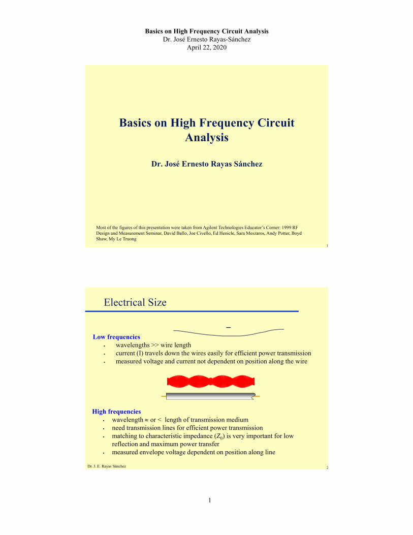
Basics on High Frequency Circuit Analysis Dr. José Ernesto Rayas-Sánchez April 22, 2020 1 1 Basics on High Frequency Circuit Analysis Dr. José Ernesto Rayas Sánchez Most of the figures of this presentation were taken from Agilent Technologies Educator’s Corner: 1999 RF Design and Measurement Seminar, David Ballo, Joe Civello, Ed Henicle, Sara Meszaros, Andy Potter, Boyd Shaw, My Le Truong 2 Dr. J. E. Rayas Sánchez Electrical Size Low frequencies wavelengths >> wire length current (I) travels down the wires easily for efficient power transmission measured voltage and current not dependent on position along the wire High frequencies wavelength or < length of transmission medium need transmission lines for efficient power transmission matching to characteristic impedance (Z 0 ) is very important for low reflection and maximum power transfer measured envelope voltage dependent on position along line I
Transcript of Basics on High Frequency Circuit Analysis
Basics on High Frequency Circuit Analysis Dr. José Ernesto Rayas-Sánchez
April 22, 2020
1
1
Basics on High Frequency Circuit Analysis
Dr. José Ernesto Rayas Sánchez
Most of the figures of this presentation were taken from Agilent Technologies Educator’s Corner: 1999 RF Design and Measurement Seminar, David Ballo, Joe Civello, Ed Henicle, Sara Meszaros, Andy Potter, BoydShaw, My Le Truong
2Dr. J. E. Rayas Sánchez
Electrical Size
Low frequencies wavelengths >> wire length current (I) travels down the wires easily for efficient power transmission measured voltage and current not dependent on position along the wire
High frequencies wavelength or < length of transmission medium need transmission lines for efficient power transmission matching to characteristic impedance (Z0) is very important for low
reflection and maximum power transfer measured envelope voltage dependent on position along line
I

Basics on High Frequency Circuit Analysis Dr. José Ernesto Rayas-Sánchez
April 22, 2020
2
3Dr. J. E. Rayas Sánchez
The Need of Transmission Line Theory
For analog circuits:
If the physical length of the transmission media is larger 10% of the wavelength of the highest frequency of interest
For digital circuits:
If the propagation time in the longest transmission path is larger than 10% of the fastest transition time
4Dr. J. E. Rayas Sánchez
Common Transmission Media
Uniform Interconnects
microstrip
h
w
coplanar
w1
w2
r
waveguide
twisted-paircoaxial
b
a
h
w
(Hewlett-Packard's RF Design and Measurement Seminar, 2000)
r

Basics on High Frequency Circuit Analysis Dr. José Ernesto Rayas-Sánchez
April 22, 2020
3
5Dr. J. E. Rayas Sánchez
Common Transmission Media (cont.)
Practical interconnects can be decomposed in segments of uniform interconnects (usually necessary)
Components(Chip + Pkg)
PCB(Motherboard)
PCB(add-in card)
Connector
(H. Heck, 2005)
6Dr. J. E. Rayas Sánchez
Common Transmission Media (cont.)
Practical interconnects have discontinuities and imperfections
(M. Resso, 2016)
Basics on High Frequency Circuit Analysis Dr. José Ernesto Rayas-Sánchez
April 22, 2020
4
7Dr. J. E. Rayas Sánchez
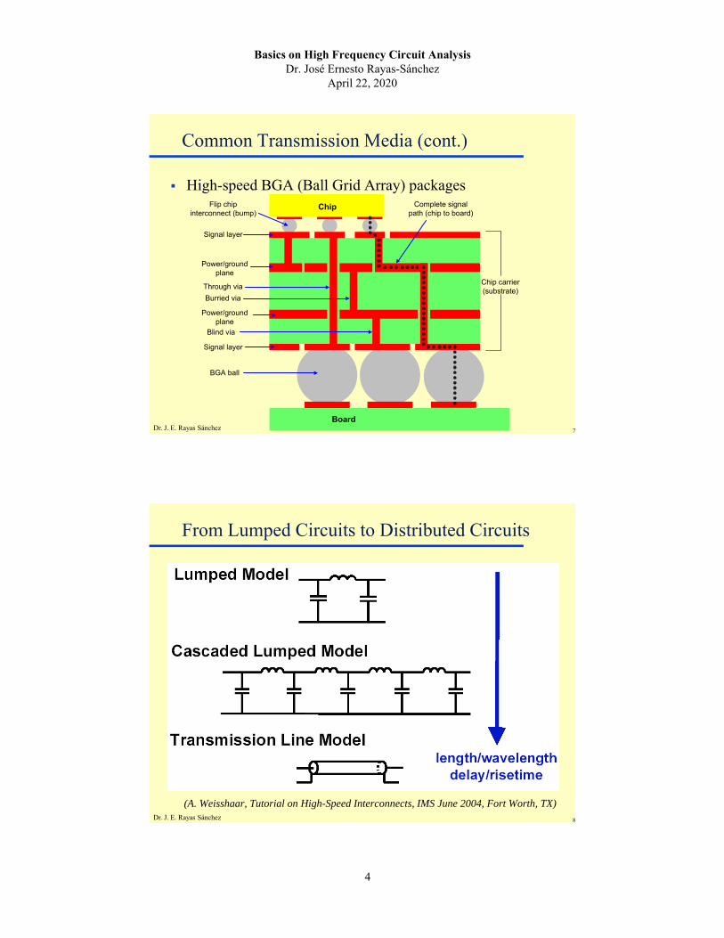
Common Transmission Media (cont.)
High-speed BGA (Ball Grid Array) packagesChip
Board
Flip chip interconnect (bump)
Signal layer
Signal layer
Power/ground plane
Power/ground plane
Through via
Burried via
Complete signal path (chip to board)
Chip carrier (substrate)
BGA ball
Blind via
8Dr. J. E. Rayas Sánchez
From Lumped Circuits to Distributed Circuits
(A. Weisshaar, Tutorial on High-Speed Interconnects, IMS June 2004, Fort Worth, TX)

Basics on High Frequency Circuit Analysis Dr. José Ernesto Rayas-Sánchez
April 22, 2020
5
9Dr. J. E. Rayas Sánchez
Transmission Line Model
The interconnect is modeled using an infinite number of RLCG sections
(R. Ludwig and P. Bretchko, RF Circuit Design, Prentice Hall, 2000)
10Dr. J. E. Rayas Sánchez
Transmission Line Model
The interconnect is modeled using an infinite number of RLCG sections
(R. Ludwig and P. Bretchko, RF Circuit Design, Prentice Hall, 2000)

Basics on High Frequency Circuit Analysis Dr. José Ernesto Rayas-Sánchez
April 22, 2020
6
11Dr. J. E. Rayas Sánchez
Transmission Line Model
Generic equivalent circuit for each section (R, L, C and G are per unit length)
The interconnect is modeled using an infinite number of these sections, making
(R. Ludwig and P. Bretchko, RF Circuit Design, Prentice Hall, 2000)
0z
12Dr. J. E. Rayas Sánchez
Transmission Line Equations
Time-Domain (Telegrapher Equations)
Telegrapher Equations in Frequency-Domain
ttzi
LtzRiz
tzv
),(),(
),(
ttzv
CtzGvz
tzi
),(),(
),(
)()()(
zILjRdz
zdV
)()()(
zVCjGdz
zdI

Basics on High Frequency Circuit Analysis Dr. José Ernesto Rayas-Sánchez
April 22, 2020
7
13Dr. J. E. Rayas Sánchez
Transmission Line Equations (cont.)
Wave equation (frequency-domain)
whereis the complex propagation constant
jCjGLjR ))((
Solutions to the wave equation are
zz eVeVzV 00)( zz eIeIzI 00)(
0)()( 2
2
2
zVdz
zVd 0)()( 2
2
2
zIdz
zId
incident wavesreflected waves
14Dr. J. E. Rayas Sánchez
Transmission Line Equations (cont.)
Solutions in the frequency domain
Solutions in the time domain
zz eVeVzV 00)(zz eIeIzI 00)(
zz eztVeztVtzv )cos(||)cos(||),( 00
Phase velocity, wave velocity or propagation speed
2p
f
v
jCjGLjR ))((
Wavelength
dtdz
vp
(speed at which a constant phase point travels down the line)

Basics on High Frequency Circuit Analysis Dr. José Ernesto Rayas-Sánchez
April 22, 2020
8
15Dr. J. E. Rayas Sánchez
Transmission Line Symbol
(Lossy) Transmission line
Length along the line
Z0,
l
Z0,
0l
ZL
z
16Dr. J. E. Rayas Sánchez
Characteristic Impedance
Characteristic impedance of the TL
CjGLjR
Z
0
0
0
0
00 I
VIV
Z

Basics on High Frequency Circuit Analysis Dr. José Ernesto Rayas-Sánchez
April 22, 2020
9
17Dr. J. E. Rayas Sánchez
Reflection Coefficient
Reflection coefficient along the line, l
Reflection coefficient at the load,
l
l
l
l eVV
eVeV
l
2
0
0
0
0)(
0L
0L
0
0
0
0)0(ZZZZ
II
VV
ll
l
l
l
l eII
eIeI
l
2
0
0
0
0)(
Z0,
0l
ZL
18Dr. J. E. Rayas Sánchez
Input Impedance
Input impedance along the line
)tanh()tanh(
)()(
)(L0
0L0in lZZ
lZZZ
lIlV
lZ
Z0,
0l
ZLZin

Basics on High Frequency Circuit Analysis Dr. José Ernesto Rayas-Sánchez
April 22, 2020
10
19Dr. J. E. Rayas Sánchez
Modeling Uniform Interconnects
(A. Weisshaar, Tutorial on High-Speed Interconnects, IMS June 2004, Fort Worth, TX)
20Dr. J. E. Rayas Sánchez
Modeling Uniform Interconnects (cont.)
Parasitic effects associated to each transmission media
– Capacitance between conductors, C
– Resistance of conductors (conductor losses), R
– Inductance of conductor loops, L
– Dielectric conductivity (dielectric losses), G
R, C, L, and G must be determined per unit length
Basics on High Frequency Circuit Analysis Dr. José Ernesto Rayas-Sánchez
April 22, 2020
11
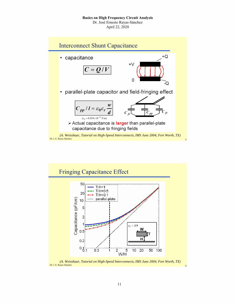
21Dr. J. E. Rayas Sánchez
Interconnect Shunt Capacitance
(A. Weisshaar, Tutorial on High-Speed Interconnects, IMS June 2004, Fort Worth, TX)
F/m) 10854.8( 120
22Dr. J. E. Rayas Sánchez
Fringing Capacitance Effect
(A. Weisshaar, Tutorial on High-Speed Interconnects, IMS June 2004, Fort Worth, TX)

Basics on High Frequency Circuit Analysis Dr. José Ernesto Rayas-Sánchez
April 22, 2020
12
23Dr. J. E. Rayas Sánchez
Interconnect Series Inductance
(A. Weisshaar, Tutorial on High-Speed Interconnects, IMS June 2004, Fort Worth, TX)
H/m) 104( 70
24Dr. J. E. Rayas Sánchez
Interconnect Series DC Resistance
(A. Weisshaar, Tutorial on High-Speed Interconnects, IMS June 2004, Fort Worth, TX)

Basics on High Frequency Circuit Analysis Dr. José Ernesto Rayas-Sánchez
April 22, 2020
13
25Dr. J. E. Rayas Sánchez
Skin Effect
(A. Weisshaar, Tutorial on High-Speed Interconnects, IMS June 2004, Fort Worth, TX)
26Dr. J. E. Rayas Sánchez
EM-Simulation of Conductor Current Distribution
(A. Weisshaar, Tutorial on High-Speed Interconnects, IMS June 2004, Fort Worth, TX)

Basics on High Frequency Circuit Analysis Dr. José Ernesto Rayas-Sánchez
April 22, 2020
14
27Dr. J. E. Rayas Sánchez
Proximity Effect
(A. Weisshaar, Tutorial on High-Speed Interconnects, IMS June 2004, Fort Worth, TX)
28Dr. J. E. Rayas Sánchez
Proximity and Skin Effects
E. Bogatin, “Essential principles of signal integrity,” IEEE Microwave Magazine, vol. 12, pp. 34-41, Aug. 2011.
Basics on High Frequency Circuit Analysis Dr. José Ernesto Rayas-Sánchez
April 22, 2020
15
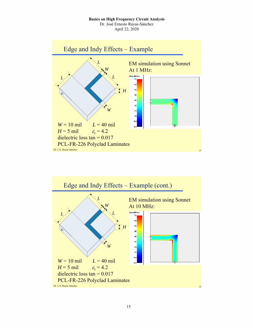
29Dr. J. E. Rayas Sánchez
Edge and Indy Effects – Example
W = 10 mil L = 40 milH = 5 mil r = 4.2dielectric loss tan = 0.017PCL-FR-226 Polyclad Laminates
EM simulation using SonnetAt 1 MHz:
rH
W
L
L
L
W
30Dr. J. E. Rayas Sánchez
Edge and Indy Effects – Example (cont.)
W = 10 mil L = 40 milH = 5 mil r = 4.2dielectric loss tan = 0.017PCL-FR-226 Polyclad Laminates
EM simulation using SonnetAt 10 MHz:
rH
W
L
L
L
W

Basics on High Frequency Circuit Analysis Dr. José Ernesto Rayas-Sánchez
April 22, 2020
16
31Dr. J. E. Rayas Sánchez
Edge and Indy Effects – Example (cont.)
W = 10 mil L = 40 milH = 5 mil r = 4.2dielectric loss tan = 0.017PCL-FR-226 Polyclad Laminates
EM simulation using SonnetAt 100 MHz:
rH
W
L
L
L
W
32Dr. J. E. Rayas Sánchez
Edge and Indy Effects – Example (cont.)
W = 10 mil L = 40 milH = 5 mil r = 4.2dielectric loss tan = 0.017PCL-FR-226 Polyclad Laminates
EM simulation using SonnetAt 1 GHz:
rH
W
L
L
L
W
Basics on High Frequency Circuit Analysis Dr. José Ernesto Rayas-Sánchez
April 22, 2020
17
33Dr. J. E. Rayas Sánchez
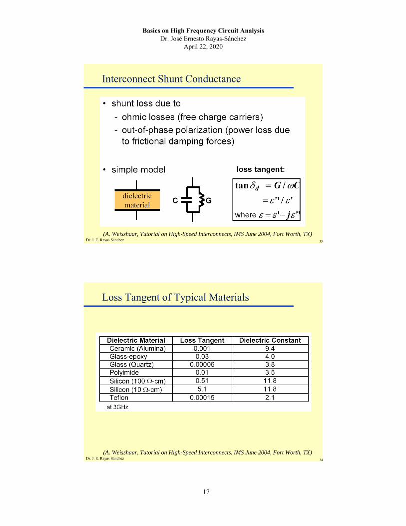
Interconnect Shunt Conductance
(A. Weisshaar, Tutorial on High-Speed Interconnects, IMS June 2004, Fort Worth, TX)
34Dr. J. E. Rayas Sánchez
Loss Tangent of Typical Materials
(A. Weisshaar, Tutorial on High-Speed Interconnects, IMS June 2004, Fort Worth, TX)

Basics on High Frequency Circuit Analysis Dr. José Ernesto Rayas-Sánchez
April 22, 2020
18
35Dr. J. E. Rayas Sánchez
Power Transfer Efficiency
RS
RL
Maximum power is transferred when RL = RS
RL / RS
0
0.2
0.4
0.6
0.8
1
1.2
0 1 2 3 4 5 6 7 8 9 10
Lo
ad
Po
wer
(no
rmaliz
ed
)
(Hewlett-Packard's RF Design and Measurement Seminar, 2000)
36Dr. J. E. Rayas Sánchez
Power Transfer Efficiency (cont.)
For complex impedances, maximum power transfer occurs when ZL = ZS* (conjugate match)
Zs = R + jX
ZL = Zs* = R - jX
Zo
Zo
Rs
RL
+jX
-jX
At high frequencies, maximum power transfer occurs when RS = RL = Zo
(Hewlett-Packard's RF Design and Measurement Seminar, 2000)

Basics on High Frequency Circuit Analysis Dr. José Ernesto Rayas-Sánchez
April 22, 2020
19
37Dr. J. E. Rayas Sánchez
The Smith Chart
-90 o
0o180
o+-
.2
.4
.6
.8
1.0
90o
0 +R
+jX
-jX
Smith Chart maps rectilinear impedanceplane onto polar plane
Rectilinear impedance plane
Polar plane
Z = ZoL
= 0
Constant X
Constant R
Z = L
= 0 O
1
Smith Chart
(open)
LZ = 0
= ±180 O1
(short)
(Hewlett-Packard's RF Design and Measurement Seminar, 2000)
38Dr. J. E. Rayas Sánchez
0.2
0.5
1.0
2.0
5.0
+0.2
-0.2
+0.5
-0.5
+1.0
-1.0
+2.0
-2.0
+5.0
-5.0
0.0
The Smith Chart – Interpretation
0L Z LZ
0L ZZ
0L jZZ
0L jZZ
(open circuit)(short circuit)
(pure inductive)
(pure capacitive)
(matched)Circles of constant XL
Circles of constant RL
0
180101
901
901

Basics on High Frequency Circuit Analysis Dr. José Ernesto Rayas-Sánchez
April 22, 2020
20
39Dr. J. E. Rayas Sánchez
Lightwave Analogy to RF Energy
RF
Incident
Reflected
Transmitted
Lightwave
(Hewlett-Packard's RF Design and Measurement Seminar, 2000)
40Dr. J. E. Rayas Sánchez
Transmission Line Terminated with Zo
For reflection, a transmission line terminated in Zo behaves like an infinitely long transmission line
Zs = Zo
Zo
Vrefl = 0 (all the incident power is absorbed in the load)
Vinc
Zo = characteristic impedance of transmission line
(Hewlett-Packard's RF Design and Measurement Seminar, 2000)

Basics on High Frequency Circuit Analysis Dr. José Ernesto Rayas-Sánchez
April 22, 2020
21
41Dr. J. E. Rayas Sánchez
Transmission Line Terminated with Short, Open
Zs = Zo
Vrefl
V inc
For reflection, a transmission line terminated in a short or open reflects all power back to source
In phase (0°) for openOut of phase (180°) for short
(Hewlett-Packard's RF Design and Measurement Seminar, 2000)
42Dr. J. E. Rayas Sánchez
Transmission Line Terminated with 25
Zs = Zo
ZL = 25
Vrefl
V inc
Standing wave pattern does not go to zero as with short or open
(Hewlett-Packard's RF Design and Measurement Seminar, 2000)
Basics on High Frequency Circuit Analysis Dr. José Ernesto Rayas-Sánchez
April 22, 2020
22
43Dr. J. E. Rayas Sánchez
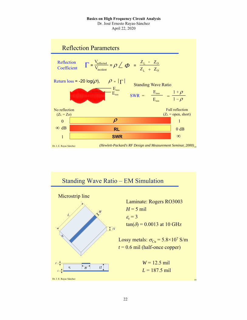
Reflection Parameters
dB
No reflection(ZL = Zo)
RL
SWR
0 1
Full reflection(ZL = open, short)
0 dB
1
=Z L - Z O
ZL + OZ
ReflectionCoefficient
=Vreflected
Vincident=
= Return loss = -20 log(),
SWR = Emax
Emin
=1 + 1
Standing Wave RatioEmax
Emin
(Hewlett-Packard's RF Design and Measurement Seminar, 2000)
44Dr. J. E. Rayas Sánchez
Standing Wave Ratio – EM Simulation
Microstrip lineLaminate: Rogers RO3003
H = 5 mil
r = 3
tan() = 0.0013 at 10 GHz
Lossy metals: Cu = 5.8×10⁷ S/m
t = 0.6 mil (half-once copper)
W = 12.5 mil
L = 187.5 mil

Basics on High Frequency Circuit Analysis Dr. José Ernesto Rayas-Sánchez
April 22, 2020
23
45Dr. J. E. Rayas Sánchez
Standing Wave Ratio – EM Simulation (cont.)
Using Zport1 = Zport2 = 50
f = 0.1 GHz f = 30 GHz
46Dr. J. E. Rayas Sánchez
Standing Wave Ratio – EM Simulation (cont.)
Using Zport1 = 50 , Zport2 = 1 K
f = 0.1 GHz f = 30 GHz
Basics on High Frequency Circuit Analysis Dr. José Ernesto Rayas-Sánchez
April 22, 2020
24
47Dr. J. E. Rayas Sánchez
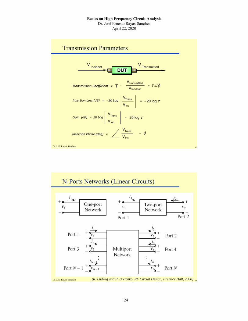
Transmission Parameters
VTransmitted
VIncident
Transmission Coefficient = =VTransmitted
V Incident=
DUT
Gain (dB) = 20 Log VTrans
V Inc
= 20 log
Insertion Loss (dB) = ‐ 20 Log VTrans
V Inc
= - 20 log
Insertion Phase (deg) =
VTrans
V Inc
=
48Dr. J. E. Rayas Sánchez
N-Ports Networks (Linear Circuits)
(R. Ludwig and P. Bretchko, RF Circuit Design, Prentice Hall, 2000)

Basics on High Frequency Circuit Analysis Dr. José Ernesto Rayas-Sánchez
April 22, 2020
25
49Dr. J. E. Rayas Sánchez
Impedance Matrix Representation (Z)
Each element of matrix Z is given by
NV
V
V
2
1
V
NI
I
I
2
1
I
ZIV
NNNN
N
N
ZZZ
ZZZ
ZZZ
21
22221
11211
Z
jkIj
iij
k
IV
Z
for 0
50Dr. J. E. Rayas Sánchez
Admittance Matrix Representation (Y)
Each element of matrix Y is given by
NV
V
V
2
1
V
NI
I
I
2
1
I
YVI
NNNN
N
N
YYY
YYY
YYY
21
22221
11211
Y
jkVj
iij
k
VI
Y
for 0

Basics on High Frequency Circuit Analysis Dr. José Ernesto Rayas-Sánchez
April 22, 2020
26
51Dr. J. E. Rayas Sánchez
Z-Parameters for 2-Port Networks
2
1
V
VV
2
1
I
II
ZIV
2221
1211
ZZ
ZZZ
Equivalent circuit:
52Dr. J. E. Rayas Sánchez
Y-Parameters for 2-Port Networks
2
1
V
VV
2
1
I
II
YVI
2221
1211
YY
YYY
Equivalent circuit:

Basics on High Frequency Circuit Analysis Dr. José Ernesto Rayas-Sánchez
April 22, 2020
27
53Dr. J. E. Rayas Sánchez
H-Parameters (Hybrid) for 2-Port Networks
2
1
2
1
V
I
I
VH
2221
1211
HH
HHH
Equivalent circuit:
54Dr. J. E. Rayas Sánchez
The Scattering Matrix (S)
NV
V
V
2
1
V
NV
V
V
2
1
V
SVV
NNNN
N
N
SSS
SSS
SSS
21
22221
11211
S
jkVj
iij
k
VV
S
for 0
Vk+ = 0 if we terminate port k with a matched load (ZLk = Z0k)
V1
I1I1
+V1+
I1V1
Z01
Vk
IkIk
+ Vk+
Ik Vk
Z0k
Basics on High Frequency Circuit Analysis Dr. José Ernesto Rayas-Sánchez
April 22, 2020
28
55Dr. J. E. Rayas Sánchez
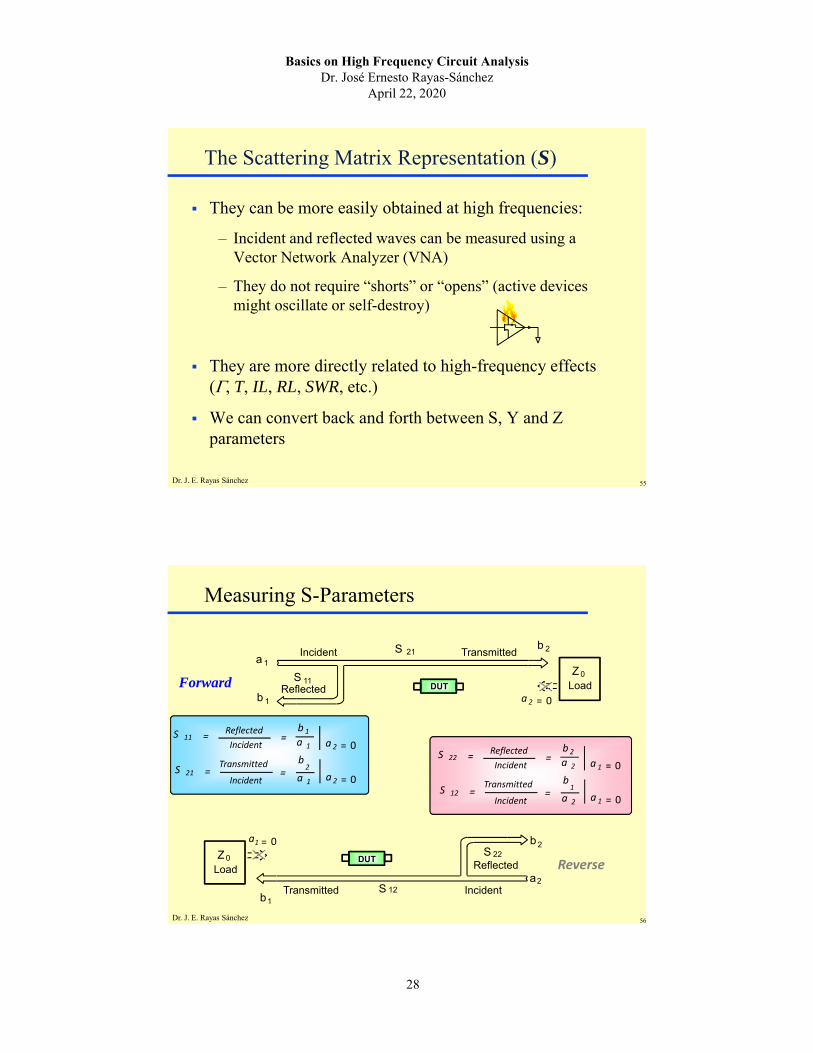
The Scattering Matrix Representation (S)
They can be more easily obtained at high frequencies:
– Incident and reflected waves can be measured using a Vector Network Analyzer (VNA)
– They do not require “shorts” or “opens” (active devices might oscillate or self-destroy)
They are more directly related to high-frequency effects (, T, IL, RL, SWR, etc.)
We can convert back and forth between S, Y and Z parameters
56Dr. J. E. Rayas Sánchez
Measuring S-Parameters
S 11 =Reflected
Incident=
b 1
a 1 a 2 = 0
S 21 =Transmitted
Incident=
b2
a 1 a 2 = 0
S 22 =Reflected
Incident=
b 2
a 2 a 1 = 0
S 12 =Transmitted
Incident=
b1
a 2 a 1 = 0
Incident TransmittedS 21
S 11Reflected
b 1
a 1
b 2
Z 0
Loada2 = 0
DUTForward
1IncidentTransmitted S 12
S 22
Reflected
b 2
a2
b
a1 = 0
DUTZ 0
Load Reverse

Basics on High Frequency Circuit Analysis Dr. José Ernesto Rayas-Sánchez
April 22, 2020
29
57Dr. J. E. Rayas Sánchez
Meaning of the S-parameters (cont.)
S11 : forward reflection coefficient (input match)
S22 : reverse reflection coefficient (output match)
S21 : forward transmission coefficient (gain or loss)
S12 : reverse transmission coefficient (isolation)
ikVi
ikVi
iii
k
kVV
S
for 0
for 0
iiiS
jiij TS jkVji
jkVj
iij
k
k
TVV
S
for 0
for 0
58Dr. J. E. Rayas Sánchez
An RF Prototype

Basics on High Frequency Circuit Analysis Dr. José Ernesto Rayas-Sánchez
April 22, 2020
30
59Dr. J. E. Rayas Sánchez
Hybrid Microwave Integrated Circuits (cont.)
M. Pozar (1998), Microwave Engineering. Amherst, MA: John Wiley and Sons.
60Dr. J. E. Rayas Sánchez
Monolithic Microwave Integrated Circuits (MMIC)
M. Pozar (1998), Microwave Engineering. Amherst, MA: John Wiley and Sons.

Basics on High Frequency Circuit Analysis Dr. José Ernesto Rayas-Sánchez
April 22, 2020
31
61Dr. J. E. Rayas Sánchez
High Speed Interconnects
J.C. Rautio, Rigorous Evaluation of Worst Case Total Crosstalk in the Time Domain Using Frequency Domain Scattering Parameters, 2001 High-Performance System Design Conference
62Dr. J. E. Rayas Sánchez
High Speed Interconnects (cont.)
J.C. Rautio, Rigorous Evaluation of Worst Case Total Crosstalk in the Time Domain Using Frequency Domain Scattering Parameters, 2001 High-Performance System Design Conference