
Basic Electronics 10ELN25 - WordPress.com Electronics 10ELN25 Dept. of ECE,SJBIT Page 4 direction is...
102
Basic Electronics 10ELN25 Dept. of ECE,SJBIT Page 1 Question Papers Solution PART –A UNIT 1 SEMICONDUCTOR DIODE AND ITS APPLICATIONS June/July 2013 1. Choose the correct answers for the following: (4 M) i. When forward-biased, a diode a) blocks current b) conducts current c) has a high resistance d) drops a large voltage ii. The knee voltage of a Silicon diode is a) 0.3 V b) 0.5 V c) 0.7 V d) None of these iii. The ripple factor of half wave rectifier is about____ a) 40.6 b) 0.46 c) 1.21 d) 81.2 iv. The rms value of a load current in case of a full wave rectifier is a) π/2 b) Im/2 c) Im/ 1.41 d) Im/π 2. With a neat circuit diagram, explain the working principles of full wave bridge rectifier. (6M) Sol: Bridge rectifier (i) Vout D1D3 D2D4 D1D3 Fig: Full wave bridge wave rectifier (i) Circuit diagram (ii) waveforms. The circuit diagram of a bridge rectifer is shown above. It uses four diodes and a transformer.
Transcript of Basic Electronics 10ELN25 - WordPress.com Electronics 10ELN25 Dept. of ECE,SJBIT Page 4 direction is...

Basic Electronics 10ELN25
Dept. of ECE,SJBIT Page 1
Question Papers Solution
PART –A
UNIT 1
SEMICONDUCTOR DIODE AND ITS APPLICATIONS
June/July 2013
1. Choose the correct answers for the following: (4 M)
i. When forward-biased, a diode
a) blocks current b) conducts current
c) has a high resistance d) drops a large voltage
ii. The knee voltage of a Silicon diode is
a) 0.3 V b) 0.5 V c) 0.7 V d) None of these
iii. The ripple factor of half wave rectifier is about____
a) 40.6 b) 0.46 c) 1.21 d) 81.2
iv. The rms value of a load current in case of a full wave rectifier is
a) π/2 b) Im/2 c) Im/ 1.41 d) Im/π
2. With a neat circuit diagram, explain the working principles of full wave bridge rectifier. (6M)
Sol:
Bridge rectifier
(i)
Vout
D1D3 D2D4 D1D3
Fig: Full wave bridge wave rectifier (i) Circuit diagram (ii) waveforms.
The circuit diagram of a bridge rectifer is shown above. It uses four diodes and a
transformer.

Basic Electronics 10ELN25
Dept. of ECE,SJBIT Page 2
During the +ve half-cycle, end A is +ve and end B is –ve thus diodes D1 and D3 are
forward bias while diodes D2 and D4 are reverse biased thus a current flows through diode D1,
load RL ( C to D) and diode D3.
During the –ve half-cycle, end B is +ve and end A is –ve thus diodes D2 and D4 are
forward biased while the diodes D1 and D3 are reverse biased. Now the flow of current is
through diode D4 load RL ( D to C) and diode D2. Thus, the waveform is same as in the case of
center-tapped full wave rectifier.
3. Draw the circuit of full wave rectifier and show that the ripple factor = 0.48 and efficiency = 81% (6 M)
Sol:
Fig: Full Wave Rectifier
Let V = Vmsinθ be the voltage across the secondary winding
I = Imsinθ be the current flowing in secondary circuit
rf = diode resistance
RL = load resistance
Efficiency=dc power output/acpower input=Pdc/Pac
dc power output
LdcRIPdc 2 -----------------------------(1)
0
.2
12 diII avdc
0
.Im2
12 dSinI av
m
av
II
2 -------------------------------------------------------- (2)

Basic Electronics 10ELN25
Dept. of ECE,SJBIT Page 3
L
m
dc RI
P
22
------------------------------------------ (3)
input ac power
Lfrmsac RrIP 2
---------------------------------------- (4)
diI rms 0
2
2
12
Squaring both sides we get
diI rms 0
22 1
2
2
2 m
rms
II
2
m
rms
II ------------------------------------------------ ----- (5)
Lf
m
ac RrI
P
2
2 --------------------------------------------(6)
Lf
L
m
m
ac
dc
Rr
R
I
I
P
P
*
2
22
2
η =
L
f
R
r1
812.0 -------------------------------------------------(7)
The efficiency will be maximum if rf is negligible as compared to RL.
Maximum efficiency = 81.2 %
Jan 2013
1. Choose the correct answers for the following: (4 M)
i. A device which allows the current flow in one direction but does not allow it in the opposite
0
22 )(Im1
dSinI rms

Basic Electronics 10ELN25
Dept. of ECE,SJBIT Page 4
direction is called ____
a) transistor b) filter
c) regulator d) rectifier
ii. The capacitance of a forward biased p-n function is called _____
a) diffusion b) conventional c) drift d) transition
iii. The zener power dissipation is given by _____
a) VRIZ b) VFIZ c) VZIZ d) none of these
iv. The maximum efficiency of full wave rectifier is ______
a) 40.6% b) 60.4% c) 78.5% d) 81.2%
2. Explain the forward and reverse characteristics for a Ge-diode with a neat figure.(5 M)
Sol:
But before we can use the PN junction as a practical device or as a rectifying device we
need to firstly bias the junction, ie connect a voltage potential across it. On the voltage
axis above, "Reverse Bias" refers to an external voltage potential which increases the
potential barrier. An external voltage which decreases the potential barrier is said to act in
the "Forward Bias" direction.
There are two operating regions and three possible "biasing" conditions for the standard
Junction Diode and these are:

Basic Electronics 10ELN25
Dept. of ECE,SJBIT Page 5
Zero Bias - No external voltage potential is applied to the PN-junction.
Reverse Bias - The voltage potential is connected negative, (-ve) to the P-type material
and positive, (+ve) to the N-type material across the diode which has the effect of
Increasing the PN-junction width.
Forward Bias - The voltage potential is connected positive, (+ve) to the P-type material
and negative, (-ve) to the N-type material across the diode which has the effect of
Decreasing the PN-junction width.
3. With a neat circuit diagram, explain the working principles of full wave rectifier. Draw relevant waveforms. (6 M)
Sol:
Fig: Full wave rectifier
The circuit diagram of a center tapped full wave rectifier is shown in fig above. It employs
two diodes and a center tap transformer. The a.c. signal to be rectified is applied to the
primary of the transformer and the d.c. output is taken across the load RL.
During the +ve half-cycle end X is +ve and end Y is –ve this makes diode D1 forward
biased and thus a current i1 flows through it and load resistor RL.Diode D2 is reverse
biased and the current i2 is zero.
During the –ve half-cycle end Y is +Ve and end X is –Ve. Now diode D2 is forward biased
and thus a current i2 flows through it and load resistor RL. Diode D1 is reversed and the
current i1 = 0.
June 2012
1. Choose the correct answers for the following: (4 M)
i. Zener diode can be used for rectification. This statement is _____
a) True b) False
c) Niether True Nor False d) None of these
ii. PIV in case of half wave rectifier for an input signal of Vm sin wt is ____
a) Vm b) 2 Vm c) Vm/2 d) Vm/ 1.41
iii. If frequency of input is 60Hz for a full wave rectifier, the frequency of ripple is ______
a) 30 Hz b) 60 Hz c) 120 Hz d) 180 Hz
iv. If peak to peak voltage is 4 V then RMS voltage is _____
a) 1.41 V b) 2 V c) 2.82 V d) Both (a) and (c)
2.
m 7 7 m (4 M)
Sol:
The current in a diode is given by the diode current equation

Basic Electronics 10ELN25
Dept. of ECE,SJBIT Page 6
I = I0( e V/ηVT –1
)
Where, I------ diode current
I0------ reverse saturation current
V------ diode voltage
η------- semiconductor constan=1 for Ge, 2 for Si.
VT------ Voltage equivalent of temperature= T/11,600 (Temperature T is in
Kelvin)
Given: I = 10mA; T=27+273=300Kelvin; η = 2; V= 700mV; VT = .02586
I0 = 36 nA
3. Explain the effect of temperature on the diode characteristics and also on the power rating of the diode. (6 M)
Sol:
The diode manufacturer specifies in the data sheet, the maximum power that can
be dissipated by the device under normal operation. If the specified level is
exceeds, then device is over heated and may get damaged.A typical derating
graph is shown in figure.
Fig: typical diode de-rating graph.
The maximum power that can be dissipated is specified for an ambient
temperature of 25 C, if the temperature of the device exceeds maximum power
dissipation then it must be derated.The maximum power dissipation for any
temperature can be read from the graph provided by the manufacturer,and is
shown in figure below.The derating factor defines the slope of power dissipation
versus temperature and is shown in figure. The derated power at P2 can be calculated
as follows:

Basic Electronics 10ELN25
Dept. of ECE,SJBIT Page 7
4. Explain the operation of full wave center tap rectifier with neat circuit diagram and waveforms (6 M)
Sol: Refer question no. 2, June/July 2013
JUNE 2011
l. Choose the correct answers for the following: (4 Marks)
i) Forward voltage across a conducting silicon diode is
A) 0.3 V B) 0.7V
C) -07V D) -03V
ii) Zener diode regulates only when it is connected in __ nlode.
A) forward bias B) reverse bias
C) Short D) Open
iii) I'm' for half wave rectifier is_
iv) Peak inverse voltage for bridge rectifier is
Ans. i)B ii)B iii) A iv)B
2. Deduce the following for FWR.
i) Irms ii) Idc iii) Ripple factor iv) Efficiency of rectification (8 Marks)

Basic Electronics 10ELN25
Dept. of ECE,SJBIT Page 8
If RL» (RF + R), then the efficiency is maximum of 81.2% but practically FWR is less than
81.2%.
3. i) Calculate the ripple voltage of a full wave rectifier with a 120 µf capacitor
connected to a load and load current of 60 mA, frequency of 50Hz.
ii) If the peak voltage of the rectified wave is 60 V, calculate the DC voltage,
iii) Calculate the ripple factor. (8 Marks)

Basic Electronics 10ELN25
Dept. of ECE,SJBIT Page 9
JANUARY – 2011
1. i)The rms value of load current in case of a halfwave rectifier is
ii) The peak increase voltage of a FWR, With centre tap transformer is
iii) In a bridge rectifier, input is from 230 V; 50 Hz; TIle DC output voltage is
A)200V B)207V C)315V D)220V
iv) The knee voltage of a Germanium diode is volts
A)0.3V B)0.5V C)0.7V D) None of these
Ans: i) B ii) C iii) B iv) A
2. Discuss the performance of the zener diode, in terms of the source & load effects.
(8 M)
The performance of a zener diode regulator can be expressed in terms of source and load
effects but if there are any input ripple voltage. The output ripple is completely eliminated.
The ripple rejection ratio is the ratio of the olp ripple voltage amplitude to input ripple,
voltage amplitude.To assess the above performance, we require AC equivalent circuit
when the zener diode is replaced by dynamic impedance. Zz as shown in fig.

Basic Electronics 10ELN25
Dept. of ECE,SJBIT Page 10
The olp resistance Ro is Ro = Zz II Rs
When load changes, the output voltage change is ∆V = ∆IL (Zz II Rs)
3. Draw the circuit of a bridge rectifier and explain its working. What is the use of
the filter (5 Marks)

Basic Electronics 10ELN25
Dept. of ECE,SJBIT Page 11
Operation:
During +tve half cycle of the ac input voltage, end A becomes positive with
respect to end B. This makes diodes DI & D2 forward biased, while DJ & D4 are
reverse biased.
Therefore only diode D1 & D2 conducts. The conventional current flows through the load
resistance RL & is shown by the arrows.
During -ve half cycle
Duing -ve half cycle of the ac i/p voltage end A becomes –ve Wrt end B. This makes
diodes D3 & D4 forward biased, while D1 & D2 are reverse biased. Therefore only diodes
D3 & D4, conducts
The conventional current flows through the load resistance IL& is shown by the arrows,

Basic Electronics 10ELN25
Dept. of ECE,SJBIT Page 12
DEC 2010
1. Select the right answer: (4 Marks)
i) What kind of a device is a diode?
a) Bilateral b) Linear
c) Nonlinear d) Unipolar

Basic Electronics 10ELN25
Dept. of ECE,SJBIT Page 13
ii) How is non-conducting diode biased?
a) Forward b) Reverse c) Poorly d) Non of these
iii) What is the value of the current (i) in the circuit shown in FigQ l(a) (iii)?
a)0.5A b) 0.4A c)0.1A d) none of these
iv) If the line frequency is 60 Hz, the output frequency of a half wave rectifier is
a)30Hz b)60Hz c) 120Hz d)0Hz
Ans: i) (b) ii) (b) iii) (c) iv) (c)
2. For a typical P-N junction diode, define the terms: i) Knee voltage and ii) Reverse
saturation current. Also indicate then on typical V-I characteristic curve.
(4 Marks)
Ans: Knee voltage:
It is the voltage at which conduction starts in pn junction diode. Below this voltage current
is very small. Knee voltage for silicon is 0.7V & germanium is 0.3V.
Reverse saturation current:
When the diode is reverse biased, minority carries cross over the junction and constitutes
current and is called as Reverse saturation current.

Basic Electronics 10ELN25
Dept. of ECE,SJBIT Page 14
3. Design a zener voltage regulator to meet the following specifications: Output
voltage = 5 V Ioad current = 10 mA zener wattage = 100 mW Input
voltage=IOV±2V (4 marks)
4. Derive an expression for ripple factor and output dc voltage, in case of a full wave
rectifier with capacitive filter (8Marks)

Basic Electronics 10ELN25
Dept. of ECE,SJBIT Page 15
Where f = frequency in Hz.
C = Capacitance in farads.
RL = load resistance in ohms.
JAN2010
1. i) The cut - in voltage of a Si - P - n diode is about...... (4 Marks)
a) 0.6V b) 0.6mV
c) 1.2V d) l.2mV
ii) The ripple factor for a full- wave rectifier is.
a) 0.482 b) 0.5
c) 1.21 d) -1.21
iii) The Zener resistance of a Zener diode, which exhibits 50mV change in Vz for a 2.5Ma
change in Iz, is
iv) The average output voltage of a half wave rectifier with an input of 300 sin 314t is
a) 100V b) 95.49V
c) 90.49 V d) 90.0 V
Ans:- i) (a) ii) (a) iii) 20Ω iv) (b)
2. Draw and explain the Y.I characteristic of Si and Ge diodes. (6 Marks)

Basic Electronics 10ELN25
Dept. of ECE,SJBIT Page 16
Ans. Silicon diode Forward & Reverse characteristic
For silicon diode. The forward current 'IF' remains very low(<μA) until the diode
forward bias voltage Vf exceeds approximately 0.7V.
Above 0.7V, 'IF' increases almost linearly with increase in VF .The diode reverse
current 'IR' is very much smaller than its forward current IF For Silicon diode, "IR"
is normally less then 100nA,and it is almost completely independent of the reverse
- bias voltage.
'IR' is due to minority change carriers and is called reverse saturation current.
When reverse bias voltage 'VR' is sufficiently increased, The diode goes into
reversebreakdown which may destroy.Reverse breakdown occurs at 75V.

Basic Electronics 10ELN25
Dept. of ECE,SJBIT Page 17
For Germanium diode, The forward current ‘If' remains very low(<μA) until the
diode forward bias voltage 'Vf' exceeds approximately 0.3V.
,Above 0.3V, 'If' increases almost linearly with increase in 'Vf’. The diode reverse
current 'IR' is very much smaller than its forward current 'If' for' Germanium
diode,IR is normally less than 1μA, and it is almost completely less independent of
the reverse - bias voltage.
IR is due to minority change carriers and is called reverse saturation current.
When reverse bias voltage VR is sufficiently increased, the diode goes into reverse
breakdown which may destroy
Reverse breakdown occurs at 50V.
3. Draw the circuit of a half wave rectifier and explain its working with necessary
waveforms. 6 Marks
Fig(a) Half wave rectifier (b) Wave forms of transformer secondary voltage ,load Current
,load voltage. '
Half wave rectifier consisted of a single diode in series with load resistance. The ac
voltage across the secondary winding A & B changes polarities after half cyc1e.
Operation :-
During positive half cycle of the ac input voltage end A becomes positive wrt end B,the
diode D is forward biased and acts as a short circuit, thus the current flows in the circuit.
The load voltage is given by

Basic Electronics 10ELN25
Dept. of ECE,SJBIT Page 18
During negative half cycle of the ac input voltage end A becomes negative wrt end B, The
Diode D is reverse biased and acts as a open circuit thus no current flows in the circuit as
shown in Fig
The dc output wave form is expected to be a straight line but the half wave rectifier gives
output in the form of positive sinusoidal pulse. Hence the output is called pulsating dc
The load current is given by

Basic Electronics 10ELN25
Dept. of ECE,SJBIT Page 19
4. A diode with Vf = 0.7v is connected as a half wave rectifier. The load resistance is
6 Ω T ( m ) 4 D m k g k
load current and the diode peak reverse voltage. 4 Marks
Given:- VF= 0.7v, RL= 600Ω, Vs= 24 V

Basic Electronics 10ELN25
Dept. of ECE,SJBIT Page 20
UNIT 2
TRANSISTORS
1. Obtain the relation between α and β of a transistor (Jan 2012, Jan 2013) (4 Marks)
2. Choose the correct answers for the following: (4 Marks)
i) When a transistor is used as a switch, it works in the following region.
A) Active and cut-off B) saturation and cut-off
C) saturation and active D) none of these
ii) If the transistor amplifier has voltage gain of 100, if the input voltage is 15mV,then the
output voltages is
A) l.5V B) 15V
C) 0.15V D) 1.15V
iii) The phase difference between input and output of an emitter follower is
A) in-phase B) out-of-phase
C)90° D)45°

Basic Electronics 10ELN25
Dept. of ECE,SJBIT Page 21
iv) An amplifier is generally connected in __ mode.
A) saturation B)cut-off
C) active D) short
Ans: i) 13 ii) A iii) A iv) C
3. A transistor amplifier connected in CE m β = IB = 50µA. Compute
the values of IC,IE α (Jan 2013)(6 Marks)
4. Draw a sketch to show the various currents in a NPN transistor and deduce the
relationship between various components. (July 2012)(10 Marks)

Basic Electronics 10ELN25
Dept. of ECE,SJBIT Page 22
In NPN transistor, electrons are injected into the base. These electrons constitute the
emitter current IE Assume that 100 electrons are injected into the base region. Since the
base is very thin, only few electrons say 2 in' number, recombine with the holes. This
constitute the base current IB .The remaining 98 electrons cross the base-collector,
constituting collector current 'Ic'.
When collector base junction is reverse biased, a very small reverse. saturation current
(ICBO) flows across the junctions, called collector to base leakage current 'ICBO'& it is very
small & can be neglected.

Basic Electronics 10ELN25
Dept. of ECE,SJBIT Page 23
JAN 2011
5. Choose the correct answer:-
i) 1he transistor operating point is along the ------
A) X-axis B) Resistance Line
C) load line D)Y-axis
ii) The transistor is used for impedance matching
A)CB B)CE
C) CC D) None of these
iii) The ------transistor has the highest power gain.
A)CE B)CC
C) CB D) None of these
iv) In a transistor the current conduction is due to carriers.
A) Majority B) Minority
C) Both A & B D) None of these
Ans:- i) C ii)C iii) B iv) C
6. Draw and explain the i/p & o/p characteristics of a PNP transistor in common
emitter configuration. (8 Marks)
If emitter is common to both I/P & 0/P, then it is called common emitter configuration Fig
shows a PNP transistor in CE mode.
In CE mode, the input current. IB and the output voltage VCE are taken as independent
variables, where as the input voltage VBE and o/p current Ic are the dependent variables
and can be represented by eqns as

Basic Electronics 10ELN25
Dept. of ECE,SJBIT Page 24
Input characteristics
In order to plot the characteristics, first collector supply Vcc is varied and VCE. is kept
constant a some value. Then for various values of VBE ,IB is observed by varying VBB .The
above same procedure is repeated for different values of VCE.Tlen the graph is drawn by
taking IB along y-axis and VBE along X-axis. These family of curves represent input
characteristics as shown in fig 1.
Input resistance or dynamic resistance can be determined from input characteristics
R varies from 600Ω to 4KΩ
Output Characteristic
In order to plot output characteristics. first base supply voltage VEB is varied and input
current is kept at some constant value then for various of VCE, o/p current IC is observed
by varying Vcc. The above same procedure is repeated for different values of IB then
graph is drawn by taking Ic along y-axis and VCE along x-axis

Basic Electronics 10ELN25
Dept. of ECE,SJBIT Page 25
Ro ranges from 10kΩ to 50 kΩ
7. Given IE = 5m α= 98 ICBO = 10 µA

Basic Electronics 10ELN25
Dept. of ECE,SJBIT Page 26
DEC2010
8. Select the right answer: (4 Marks)
i) In a CE configuration circuit if the base resistor is open the Q-point will be:
a) In the middle of the load line b) At the upper end of the load line
c) At the lower end of the load line d) OFF the load line
ii) In a BJT the collector current is 10 mA, if the current gain is 100, the base current is
a)1µA b)I0µA c) 100 µA d) 1 mA
iii) Find the collector in the circuit shown in Fig. Q2(a) (iii)
a)2mA b)3mA c) 10mA d) None of these
Ans: i) (c) ii) (c) iii) (d) iv) (b)
9. For the CE circuit shown below in Fig.Q2(b), draw the DC load line and mark the
dc operating point in the active region. Indicate respective VCEQ and ICQ values
Given β = (July 2012)(6 Marks)

Basic Electronics 10ELN25
Dept. of ECE,SJBIT Page 27
10. Explaining the input and output characteristics for a CE configuration BJT
circuit. Discuss each region on the characteristics. (July 2013)(6 Marks)

Basic Electronics 10ELN25
Dept. of ECE,SJBIT Page 28
In CE configuration transistor, .emitter terminal is made common to both input and output.
Input voltage is applied between base & emitter terminals and the output is taken from
collector & emitter terminals.
Input characteristics:
The input characteristics are the graph plotted between base current (IB) and input voltage
(VBE) keeping VCE as constant. VBE is increased in steps and the graph is plotted. At a
particular point, VBE= 0.6V, base current is progressively less for increasing VCE Higher
VCE produces greater penetration into the base, reducing the distance b/w CB & EB
depletion regions.
Output characteristics:
It is the graph plotted b/w collector current (Ic) and collector to emitter voltage (VCE)
keeping base current as constant. We can see that as VCE increased from zero, Ic increases
gradually and remains constant. A small amount of Ic flows even when IB = 0. It is called

Basic Electronics 10ELN25
Dept. of ECE,SJBIT Page 29
leakage current from collector to emitter with base open (ICEO). This is called cut-off
region. when VCE has a very low value, the transistor is said to be. Saturated and it
operates in saturation region.
11. Compare various BJT circuit configurations
CB Configuration
CE Configuration

Basic Electronics 10ELN25
Dept. of ECE,SJBIT Page 30
CC Configuration:

Basic Electronics 10ELN25
Dept. of ECE,SJBIT Page 31
JAN 2010
12. i) The doping of the emitter region of a transistor is---------- the base region
a) Greater than b) Equal to
c) Less than d) Much less than
ii) If α = 0.95, Then the value of β of the transistor is ---------------.
a) 190 b)19
c) 0.05 d) 25
iii) The input resistance is highest for ------------ .
a) CB amplifier b) CC amplifier
c) CE amplifier d) None of These
iv) For cascading one should use --------------
a) CE configuration b) CB configuration
c) CC configuration d) None of these
13. Draw a block diagram of an un - biased n . p - n transistor. Identify each part of
the device and show the depletion regions and barrier voltages. Briefly explain. (5
Marks)
When the three terminals of' the transistor are kept open it is called unbiased transistor. An
unbiased· transistor means a transistor with no external voltage applied. Thus no current
flows in any of transistor leads.
During Diffusion Process region penetrates more deeply into the lightly doped
base. The depletion region at emitter junction penetrates less in the heavily doped emitter.
Similarly the depletion region at collector junction penetrates less in the heavily doped
collector and extends more in base region
This depletion layer width at the collector junction is more than the depletion layer
width at the emitter junction.

Basic Electronics 10ELN25
Dept. of ECE,SJBIT Page 32
.
The collector current Ic in terms of IE and αdc given by
Ic= αdc IE
The collector current Ic in terms of IB & αdc is given by
αdc is defined as the ratio of the collector current 'Ic' to emitter current 'IE '
Typical value of αdc , is between 0.96 to 0.995
βdc is defined as the ratio of the collector current 'Ic' to the base current 'IB

Basic Electronics 10ELN25
Dept. of ECE,SJBIT Page 33
Typical value of βdc is between 25 to 300
15 F g m g ( ) S β= 5 D
the d.c load line and determine the operating point. (6 Marks)

Basic Electronics 10ELN25
Dept. of ECE,SJBIT Page 34

Basic Electronics 10ELN25
Dept. of ECE,SJBIT Page 35
UNIT 3
BIASING METHODS
JUN 2011
1. Choose the correct answers for the following: (4 Marks)
i) Which is the bias technique that is very widely used
A) fixed B) collector
C) emitter D) Voltage divider
ii) Which transistor bias circuit has poor stability because its Q-point varies with βdc?
A) collector feedback B) base. C
C) voltage divide D) emitter
iii) Emitter follower is a
A) Voltage amplifier B) current amplifier
C) attenuator D) none of these
iv) Emitter follower has an input of I volt, then its output voltage is_
A) 0.5 V B)10V
C) 1V D) 5V
Ans. i) D ii) B iii) D iv) C
2. Explain the connect of voltage divider bias technique using transistor.
(Jan 2011)(10M)
Ans:- In precise circuit analysis the voltage divider circuit consisting of R1 and R2 must be
replaced with its thevenin equivalent as shown in fig

Basic Electronics 10ELN25
Dept. of ECE,SJBIT Page 36
Consider fig (a),here R1 and R2 should be replaced by Thevenins resistance RT and
thevenins voltage VT.The Thevenins resistance RT can be determined by setting the dc
supply to Zero voltage, where RT is a Parallel combination of R1 and R2.

Basic Electronics 10ELN25
Dept. of ECE,SJBIT Page 37

Basic Electronics 10ELN25
Dept. of ECE,SJBIT Page 38
3. A collector to base circuit has VB = 24V RB = 8 KΩ CE = 10V.Calculate hFE
,determine VCE; when a new transistor is replaced having hFE = 120. (6 Marks)
JAN 2011
4. Choose the' correct answer (4 Marks)
i) The reverse saturation current doubles for every ------ degree rise in temperature
A) 40 B)45.

Basic Electronics 10ELN25
Dept. of ECE,SJBIT Page 39
C)10 D)30
ii) The intersection of DC load line and the o/p characteristics of a transistor is called .
A) Q point B)QUlscent pomt
C) Operating Point D )AJI of these
iii) For an emitter follower, The voltage gain is __
A) Unity B) Greater than unity
C) Less than unity D) Zero
iv) The operating point must be ------for the proper operation of the transistor.
A) High B) Stable .
C) Increasing D) Decreasing
Ans:- i) C ii) D iii) A iv) B
5. Design the collector to base circuit for Fig Q3 (C) Given Vcc=20 Vi VCE=5V, IC =6
mA, hfe=100 (July 2012)(4 Marks)

Basic Electronics 10ELN25
Dept. of ECE,SJBIT Page 40
6. Explain the DC load line and operating point, with example, related to the
transistor. Consider the common emitter circuit shown in Fig (Jan2013)(4 Marks)

Basic Electronics 10ELN25
Dept. of ECE,SJBIT Page 41
The intersection points on the load line is called operating point or quiescent point, Q-
point.
DEC2010
7. Select the right answer:
i) Majority carriers in the emitter of pnp transistor are
a) Holes b) Free electronics c) Trivalent atoms d) Pentavalent atoms
ii) Voltage divider bias is noted as

Basic Electronics 10ELN25
Dept. of ECE,SJBIT Page 42
a) Unstable collector voltage b) Varying emitter current c) Large base current d)
Stable Q-point
iii) In a PN junction a temperature change of 10° C results In ....... of reverse leakage
current
a) Doubling b) Tripling c) No change d) Both B and C
iv) Thermal run away in a UJT is a
a) Useful phenomenon b) Tolerable phenomenon c) Destruction phenomenon
d) Both A and B
Ans: i) (b) ii) (d) iii) (a) iv) (c)
8. Draw a voltage divider bias circuit and derive an expression for its stability factor.
(July 2013)(8M)
The above circuit represents voltage divider bias circuit. The resistors Rc & RE are
connected in series with transistor. RE provides stabilization.

Basic Electronics 10ELN25
Dept. of ECE,SJBIT Page 43
9 = 5 R = 5 6 kΩ RB= 8 KΩ E=5
Determine the transistor hfe value. Assume a silicon transistor. (July 2012)(4 Marks)
Ans: When there is a change in temperature, the reverse leakage current also changes. For
every100 C rise in temperature, ICBO gets doubled. 1his causes the collector junction
temperature to rise, which in turn increases ICBO. This increase in ICBO causes increase in
collector current Ic which leads to further increases in ICBO. This could result in a
significant shift in the Q point as in the extreme case, the ratings of transistor are exceeded
& device burns out. This effect is called thermal runaway.
JAN 2010
10. i) For an emitter follower, the voltage gain is 4 Marks
a) Unity b) Greater than Unity
c) Less than Unity d) Zero
ii) The self bias arrangement gives a better Qpoint stability when--------------
a) Re is small b) β is small but Re is large
c) Both β and Re are large d) None of these
iii) The load line moves parallel to itself on the CE output characteristics of a transistor
when-----------
a)'RL changes b) Vcc changes
c) Both RL and Vcc changes d) None of these changes
iv) To work as a linear amplifier a transistor must operate in .
a) Active region b) Saturation region
c) Nonlinear region d) Cut - off region
Ans. i) (a) ii) (b) iii) (b) iv) (a)
11. Compare base bias, collector to base bias, and voltage divider bias with regard to
stability of the transistor collector voltage with spread in hFE value. 10 Marks

Basic Electronics 10ELN25
Dept. of ECE,SJBIT Page 44
12. Design a collector to bias circuit shown in fig with the following hfe = 100, VBE =0.7V,
Vcc = 15V (Jan 2013)(6 M)

Basic Electronics 10ELN25
Dept. of ECE,SJBIT Page 45

Basic Electronics 10ELN25
Dept. of ECE,SJBIT Page 46
UNIT 4
OTHER DEVICES
JUN 2011
1. Choose the correct answers for the following: (4 marks)
i) The function of gate in SCR is to control the _
A) flow of current B) Voltage regulation
C) voltage amplification D) none of these
ji) η ofUJT is known as ratio.
A) ON B) pulse
C) negative D) intrinsic stand - off
iii) The minimum point in V-I characteristic of UJT is known as _point.
A) negative B) valley
C) latching D) firing .
iv) For a JFET, the value of VDS, at which ID becomes essentially constant is the
A) Pinch off voltage B) Cut off voltage
C) breakdown voltage D) ohmic voltage
Ans. i) A ii) 0 iii) B iv) A
2. Explain V-I characteristic of SCR. (Jan 2011 & Jan 2010) (8 marks)
Ans:-

Basic Electronics 10ELN25
Dept. of ECE,SJBIT Page 47
Reverse Characteristics,
Fig (a) shows an SCR with a negative voltage applied to the anode w.r.t to the cathode and
gate terminal open.This reverse biases the SCR causing junction J1 and J3 to be reverse
biased and junctions J2 to be forward biased.
For small values of negative voltage of VAK,only a small reverse leakage current IRK flows
through the device, when the magnitude of the reverse –ve voltage VAK is increased, IRK
remains almost constant until a value called reverse. breakdown voltage VBE is reached,
where reverse biased junctions J1 and J3 undergo breakdown & the reverse current IR rises
rapidly, which will damage the device due to excessive heating caused by the excessive
current.
When the SCR is forward biased junction J1 and J3 become forward biased while J2 is
rev.biased and, small forward leakage current flows through the SCR.When the forward
voltage VAK is made. Large enough the reverse biased junction J2 breaks down & a large
current flows through the junctions.
With SCR forward biased if a small positive gate current is applied, it causes the SCR to
switch on at a forward anode to cathode voltage less than the forward break over voltage.
The forward voltage at which the SCR switches to on state is inversely proportional to the
magnitude of the gate current.
3. Explain working principle of U]T. (Dec 2010, July 2012) (8 marks)

Basic Electronics 10ELN25
Dept. of ECE,SJBIT Page 48
Principle of Operation:. Voltage VBB is applied between B2 & B1 and B2 is positive with
respect to B, and VE is applied between emitter 'E' and B, .If the emitter voltage VE is less
than VD +η VBB the emitter base junction is reverse biased and is as shown in fig.
A reverse current IEO flows when VE= VD +η VBB at point 'C' Ic is positive and emitter
base junction conducting at point 'C' is called peak point and the respective current is
called peak current.
As VE = VD1 +η VBB holes are injected into 'n' channel lowering the resistance of RB1
lowering the potential at A1,IE increases but voltage across the device drops here the holes
have a longer life time. Therefore number of carriers in the base region increases rapidly.
Thus potential at 'A: falls but current Ic increases rapidly. RB1 acting as a decreasing
resistance and reaches point 'd' for then increases in Ic is accomplished by a rise in VE is
called valley point 'd'. The Vv and Iv are the corresponding emitter potential and current.
Since the negative resistance region is used for switching UJT & for triggering SCR after
the point 'd' the device acts as a normal diode. since the base region is saturated &
RB1doesn't decrease again.
JAN 2011
4. Choose the correct answer:- (4Marks)
i) A SCR has __ number of junctions.
A) one B) two
C) Three D)Four
ii) The FET is a Controlled device.
A) Voltage B) current
C) power D) None of these

Basic Electronics 10ELN25
Dept. of ECE,SJBIT Page 49
iii) The holding current in a SCR is __ than the latching current.
A) More B) less
C) equal D) None of these
iv) A Relaxation oscillator uses.
A) MOSFET B) SCR
C) UJT D)BJT
Ans:- i) C ii) A iii) B iv) C
5. Explain the P-Channel JFET Drain Characteristics. (Jan 2013)(4Marks)
The Typical Drain characteristics of a p-channe1JFET
Fig shows the drain characteristics (VDS versus ID) of a p channel JFET. These
characteristics are similar to those of an n channel JFET except for the voltage polarities.
Here, the gate· cathode voltage, (VGS) levels are +ve while drain source voltage (VDS)
levels are negative. As shown in Fig VGS = 0.5V produces a higher value of ID than
VGS = 0 However, forward bias at the gate-channel junctions should be normally avoided.
Hence, negative values of VGS are not used with a p - channel JFET.
6. Explain the JFET as an amplifier. (July 2013)(8Marks)

Basic Electronics 10ELN25
Dept. of ECE,SJBIT Page 50
The drain and source terminals are connected by a dc supply (VDD) connected resistor RD
The gate and source junction is reverse biased by a DC supply (VGG).An ac voltage vi is
connected in series b/w VGG and gate terminal. A small change in the reverse bias on the
gate produces a large change in the drain current. When the ac Signal goes positive, the
reverse bias on the gate decreases. This increases the channel width and thus causes an
increase in the drain current when the ac signal goes -ve the rev. voltage on. The gate
increases which decreases the drain current. Thus a small change in gate voltage (∆VGS)
produces a large change in drain current (∆ID) & this causes a large variation in the
voltage drop across the load resistor RD connected in series with the drain terminal, In this
way JFET acts as a voltage amplifier.
DEC2010
7. Select the right answer: (4Marks)
i) The minimum anode current that keeps a thyristor turned ON is called the
a) Holding Current b) Break over current
c) Trigger current d) Latching current
ii) Input impedance of JFET
a) Approaches to zero b)Approaches one
c) Approaches to infinity d)Is impossible to predict
iii) A unipolar transistor uses
a) Both free electrons and holes b) Only free electrons
c) Only holes d) Either one or the other but not both
iv) JFET acts like a voltage controlled resistance in ------------- region.
a) Cut off b) ohmic region
c)Saturation d) None of these
Ans: i) (d) ii) (a) iii) (d) iv) (b)
8. Is continuous gate current necessary to switch the SCR ON? Justify. How the SCR
is switched OFF (July 2013)(4 Marks)

Basic Electronics 10ELN25
Dept. of ECE,SJBIT Page 51
A short duration pulse of gate current is sufficient to switch the SCR on. Once the
SCR is switched on,the gate has no further control on the device and the device continues
to conduct even when the gate current is made zero
The SCR turns off when the device current falls below a minimum value called the
holding current. This can be effected by increasing the anode circuit resistance or
decreasing the anode circuit supply voltage.
9. Illustrate SCR as a controlled rectifier (July 2012)(6 Marks)

Basic Electronics 10ELN25
Dept. of ECE,SJBIT Page 52
The gate input Signal is called trigger Signal. When once the SCR is triggered by a
positive signal, the SCR. conducts heavily & it acts as a p - n diode.The current can be
limited only by having an external resistor RL in the anode circuit. To turn the SCR OFF,
we have to reduce the anode current below the holding current.
Let us consider an SCR connected series with a resistive load to a single phase AC
voltage as shown in Fig (a). If the SCR is replaced by semiconductor diode, it will act as a
half wave rectifier the output will be half rectified. However, by applying gate trigger
signal to SCR at any time during positive half cycle of input, the device will go into
conduction.
The conduction will be there from the instant of trigger Signal application to the positive
half cycle and then switches off when magnitude of the supply voltage become zero.
At an instant wt = Ө, the trigger input is applied, the SCR turns ON i.e it goes into
conduction state. When SCR, turns ON. The output voltage falls back to VF as shown in
Fig (b).
During the negative half cycle of input SCR is in the reverse blocking state and it will not
conduct. At the next trigger input again the SCR turns ON as shown in Fig (a). The
corresponding load current waveform is also show in Fig (b).The SCR does not conduct is
OFF. The load current exists during conduction and in the non conduction state it is zero.
JAN 2010
10. i) The FET is a controlled device
a) Current b) Voltage c) Power d) None of
ii) Which of the following devices is expected to have the highest input impedance?
a) MOSFET b) BJT c)JFET
iii) The SCR is used as a
a) Ordinary rectifier b) Controlled rectifier
c) Amplifier d) None of there
iv) An initial saturated dram current can be attained in an n-channel JFET when VGS is
equal to--
a) Pinch off voltage b). Zero volts c)-4V
Ans: i) B ii) C iii) B iv)A
11. Draw a circuit diagram to obtain the drain characteristics of an n - channel JFET. Thus
draw drain characteristics & explain them. (Jan 2013)(8 Marks)

Basic Electronics 10ELN25
Dept. of ECE,SJBIT Page 53
A family of drain characteristics for an n-channel FET can be obtained by applying several
values of negative gate· source Voltage VGS' Fig shows such a family of drain
characteristics.
With VGS = 0, ID=0 and the channel between the gate junctions is entirely open as
there is no depletion region penetration. For small applied voltage VDS (< 1V) a small
drain current flows causing some Vge drop along the channel. As a result there is a small
depletion penetration of the channel, which has no appreciable effect on the width of the
channel & its resistance.
When VGS = -1V The gate - channel junctions become reverse biased on even
when ID= 0, Hence there is already a depletion penetration into the channel. Due to this,
with VGS = - 1V the channel pinch - off occurs at a lower ID value than when VGS = 0 This
the result of applying negative gate bias is to reach the saturation level at a lower level of
VDS ,as VGS is made more & more negative saturation level of ID reduces further and the
pinch - off voltage continues to drop in a parabolic manner as indicated by the dashed line
on the characteristics in Fig
It is seen that a gate - source bias Vg , equal to the pinch - off voltage (VGS = - Vp)
reduces ID to Zero (i.e. switches the device off).This value of gate bias voltage, is known
as the gate cutoff voltage VGS (off).

Basic Electronics 10ELN25
Dept. of ECE,SJBIT Page 54
The region to the left of pinch – off lows is referred to as the voltage controlled
resistance. or ohmic region, where the ]FET can be used as a voltage controlled resistor.
The region to the right of the pinch - off is normally employed in amplifiers, the value of
VDS at which break down occurs is reduced as the negative gate - source voltage is
increased.

Basic Electronics 10ELN25
Dept. of ECE,SJBIT Page 55
PART B
UNIT 5
AMPLIFIERS AND OSCILLTORS
JUN 2011
1. Choose the correct answers for the following.
i) Cut-off frequencies of an amplifier are also caIled as
A) half power points B) square points
C) amplified points D) none of these
ii) The objective of using a crystal oscillator is to get
A)DC B) 50·70 Hz
C) stable frequency D) variable frequency
iii) An oscillator uses
A) negative feedback B) +ve feedback
C) +ve and -ve feedback D) none of these
iv) Which of the following oscillators is used to generate high frequencies:
A) RC-phase shift B) Wein bridge
C) L-C oscillator D) blocking oscillator
Ans. i) A ii) B iii) C iv) C
2. Explain Barkhausen criterion. (2 Marks)
Ans:- The Barkhausen criterion states that
1) The total phase shift around a loop, as the signal proceeds from input through amplifier
Feed back network & back to again o/p is precisely a or 360 degree
2) The magnitude of product of open loop gain and magnitude of feedback factor B is
unity i.e lABl=1
3. In a Hartley oscillator L1 = 20 µH, L2 = 2 mH and capacitor is variable. Find the
range of C if frequency is varied from 1MHz to 2.5MHz.

Basic Electronics 10ELN25
Dept. of ECE,SJBIT Page 56
JAN 2011
4. Choose the correct answer
i) In a mid freq, band, the voltage gain is-------
A) increasing B) decreasing
C) constant D) None of these
ii) A crystal oscillator finds use, when the -------stability is required.
A) Amplitude B) Frequency
C) phase D) None of these
iii) The Colpit’s oscillator is -------
A) Audio oscillator B)Radio Oscillator
C) Microwave oscillator D)None of these
iv) In an oscillator, we use
A) Positive B)Negative
C) Unity gain D)None of these
Ans:- i) C ii) B . iii) B iv) A
5. With the help of a neat circuit diagram, explain the function of every component in
an RC coupled amplifier. (Repeated in jun2011, jan 2010,dec 2010)(8 Marks)

Basic Electronics 10ELN25
Dept. of ECE,SJBIT Page 57
The necessary biasing is provided by resistors R1, R2 and RE. The resistor R1 & R2 forms a
voltage divider bias & this will select the proper operating point of an amplifier.
C1 and C2 are dc blocking capacitors or coupling capacitors. C1 blocks the dc component
of the input signal Vs, if any from reaching the base of the transistor. Without C1 this dc
component disturbs the dc operating point of the transistor. C2 blocks the dc current from
reaching the load RL.
BYPASS CAPACITOR CE
Without the bypass capacitor CE , ac negative feedback is introduced through RE. This
reduces the voltage gain which is undesirable.
RC:· To achieve large voltage gain we can use large Rc.Large Rc reduces the collector
current Ic. A fairly minimum value of Ic is 1mA.
6. Draw and explain RC phase shift oscillator. , (July 2012)(4 Marks)
RC phase shift oscillator is a low frequency which is used to generate oscillator in the
audio frequency range. The circuit of Transistor RC phase shift oscillator is shown in fig.

Basic Electronics 10ELN25
Dept. of ECE,SJBIT Page 58
It consists of a single stage BJT common emitter amplifier and three cascaded
identical Rc sections which performs functions of feedback and inverting network.
Resistors R1 and R2 are used to bias the transistor properly in the active region so
that the signal Vi is faithfully amplified by the transistor amplifier note that Vi is nothing
but the signal Vp produced by the Rc network.RE is used to provide stability of the
operating point.Rc is properly selected to obtain the required voltage gain Av,C1 & C2 are
dc blocking or coupling capacitors & CE is the emitter bypass capacitor. CE is used to
prevent the loss of voltage gain due to negative feedback through RE. The amplifier
produces 180o
phase shift between Vi & Vo. Additional phase shift of 180o
b/w Vo and
Vf is produces by the cascaded RC network
7. Calculate the freq of oscillations of a Hartely oscillator having L1=0.5mH,L2=1mH
= μF (July 2013)(4 Marks)
Freq of oscillators is given by

Basic Electronics 10ELN25
Dept. of ECE,SJBIT Page 59
DEC 2010
8. Select the right answer:
i) An oscillator always needs an amplifier with
a) Positive feedback b) Negative feedback
c)Both a and b d)A LC tank Circuit
ii) Overall voltage gain with negative feedback (ACl. ) in terms of open gain (AOL ) and
Feedback factor(β) are given by
iii. For high frequency oscillators normally --------------elements are used in the feedback
circuit.
a) LC b) RC
c) Either a and b d) Both a and b
iv. Frequency output of an RC phase shift oscillator is given b

Basic Electronics 10ELN25
Dept. of ECE,SJBIT Page 60
Ans: i) (a) ii) (a) iii) (a) iv) (b)
9. Discuss the effect of negative feedback on the bandwidth an amplifier and voltage
gain of an amplifier (Jan 2013)(6 Marks)
From the graph we can explain that, when the negative feedback is applied, the amplifier
gain is reduced, since the bandwidth product has to remain the same in both the closes, it
is obvious that the bandwidth must increase to compensate for the decrease in gain.

Basic Electronics 10ELN25
Dept. of ECE,SJBIT Page 61
JAN 2010
10. i) An audio amplifier works over the frequency range -----
a) 20HZ to 20KHZ b) 20HZ to IMHZ
c) 1KHZ to 4KHZ
ii) An oscillator requires ----------feedback for its operations.
a) Negative b) Positive
c) High d) Low
iii) The frequency of a Hartley oscillator for L1 = L2= 50mH and C = 200pF' is --------
a) 503kHZ b) 100KHZ .
c) 150KHZ
iv) The conditions Aβ = 1 for oscillations is known as ----------criterion
a) Nyquist's b) Barkhausen
c) Routh - houwitz d) None of these
Ans:- i ) a ii) b iii) a iv) b
11. List and explain the advantages of negative feedback in amplifier. (July 2013)(6 M)
Sol: The following are the advantages of negative feedback
1. Negative FB stabilizes the voltage gain of an amplifier.

Basic Electronics 10ELN25
Dept. of ECE,SJBIT Page 62
2. Negative FB modifies the i/p & olp impedance of the amplifier. For instance the
series voltage negative increases olp impedance by a factor (1+βAv) & reduces the 01p
impedance by the same factor which is desirable.
3. Negative FB increases the bandwidth of an amplifier by a factor (1+βAv). This
makes the amplifier to amplify a wide range of frequencies with equal gain,
4. Negative FB reduces Harmonic distort ion by a factor (1+βAv).As a result the
olp signal is an exact replica of the ilp signal.
5. Negative FB reduces the attenuation distortion by a factor (1+βAv)
6. Negative FB reduces the noise generated with in the feedback loop of amplifier
by a factor (1+βAv)

Basic Electronics 10ELN25
Dept. of ECE,SJBIT Page 63
UNIT 6
OPERATIONAL AMPLIFIERS
JUN 2011
1. Choose the correct answers for the following:
i) An ideal OP - AMP has
A) infinite input impedance B) infinite voltage gain
C) zero output resistance D) all of these
ii) The differential amplifier has
A) one input and one output B) two inputs and two outputs
C) two inputs and one output D) One in.put and two outputs
iii) An OP-AMP shorted between inverting terminal and output terminal is called
A) adder B) voltage follower
C) integrator D) inverter
iv) The voltage gain of all OP-AMP in the op~n loop condition is of the order of
A) 101
B) 102
C) 104 D) 10
6
Ans: i)A ii)C iii)B iv)D
2.Draw the following circuits using OP-AMP (8 Marks)
i) adder ii) voltage follower iii) integrator iv) differentiator

Basic Electronics 10ELN25
Dept. of ECE,SJBIT Page 64

Basic Electronics 10ELN25
Dept. of ECE,SJBIT Page 65
3. Explain the working of CRT. (Jan 2013, July 2013)(8M)
Ans:- Cathode Ray tube( CRT)
It is the heart of CRO. The cross-sectional view of a general purpose CRT is shown in Fig
Electron Gun Assembly: It consists of an indirectly heated cathode, K, a control grid G
and accelerating anodes A1,A2 & A3. The function of the electron gun assembly is to give
a focussed narrow beam of electrons which is accelerated towards the flourescent screen.
The electrons are emitted from the cathode K due to the thermionic emission. The control
grid G is kept at negative potential with respect to cathode K. The number of electrons
allowed to pass through the grid depends on the amount of the control grid bias. The
anodes Al and A3 which are at positive potential with respect to cathode K accelerates the
electron beam. The cylindrical focussing anode A2 which is at negative potential repels
electrons from all sides and compresses
them into a narrow fine beam.
Deflecting plates: There are two sets of deflecting plates which are used for deflecting the
narrow beam both in the vertical and horizontal directions. The Y-deflecting plate (or
vertical deflecting plates) deflects the electron beam in the vertical direction and the X-
deflecting plate (or horizontal deflecting plates) deflects the electrons beam in the
horizontal direction. When no potential is applied across the plates, without any deflection
and produces a bright luminous spot at the centre of the screen.If the potential of an upper
Y-plate is made positive, the beam is deflected upwards depending on the value of an
applied potential. Similarly, if the potential of lower Y-plate is made positive the beam is
deflected downwards. However, if an alternating voltage is applied across the Y-plates,
the beam keeps moving up and down thereby producing a luminous trace of vertical
straight line on the screen. The maximum displacement of the luminous spot from its
central position is directly proportional to the amplitude of the applied voltage to the Y-
plates.
Similarly, the luminous spot on the screen is deflected horizontally, if voltages are applied
to the X-plates. In general, the signal to be displayed on the screen is applied across the Y-

Basic Electronics 10ELN25
Dept. of ECE,SJBIT Page 66
plates. The voltage applied across the X-plates is a ramp (sawtooth) voltage which is
obtained from the sweep generator.
Glass Envelop: It is funnel shaped and has a flourescent screen at its flared end. It is
highly evaluated. The inside of the flared part of the tube is coated with a conducting
graphite layer called Aquadag. In addition to accelerating the electron beam, it also
collects the electrons produced by secondary emission when electron beam strikes the
screen. Thus it prevents the formation 'of negative charges on the screen.When the highly
accelerated narrow electron beam hits the flourescent screen, the kinetic energy of
electrons is converted into light, thereby producing a bright luminous spot on the screen.
The colour of the luminous spot depends on the type of phosphor used in the fluorescent
screen.
JAN 2011
4. Choose the correct answer:-
i) The op- amp can amplify.
A) AC signal only B)DC signal Only
C) Both AC & DC signals D)None of these
ii) An op-Amp has __ output impedance
A)Infinity B)0
C) 10,000 D)600
iii) CMRR should be
A) Unity B) Zero
C) Much larger than unity D) much smaller than unity
iv) The inverting amplifier circuit has R1= 1KΩ and Rf= 3KΩ.The olp voltage is ----when
Vi=4V:
A)6V B) 16V C) 12V D) 18V
Ans:- i) A ii)B iii) C iv) C
5. Explain the term op _Amp. List the characteristics of an ideal op-amp (repeated in
Jan 2010, Dec 2010, July 2012) (8 M)
An operational amplifier or op-amp is a direct coupled multistage, voltage amplifier with
an extremely high gain. Its behavior can be controlled by adding suitable feedback. It has
a very high input in1pedance and a very low olp impedance.
Characteristics of an ideal op - Amp
1.The open loop voltage gain is infinity.
2. 'The input impedance is infinity.

Basic Electronics 10ELN25
Dept. of ECE,SJBIT Page 67
3. Output impedance is zero.
4. The bandwidth is infinity.
S. The output voltage is zero when both inputs are equal, i.e. zero off voltage.
6. Infinite CMRR
7. The slew rate is infinity.
6. Explain clearly how op-amp can be used as the following type of amplifier. (8M)
i) Summer ii) integrator iii) differentiator iv) inverting amplifier. (Jan 2013, July 2012)
i&iv) Summer & inverting amplifier are explained previously.
ii) Integrator
• In an Integrator circuit, the output voltage is the integration of the i/p voltage.
• From Virtual ground concept VA= VB= 0
• As I/P current of op . amp is zero, the entire current I flows through C1

Basic Electronics 10ELN25
Dept. of ECE,SJBIT Page 68

Basic Electronics 10ELN25
Dept. of ECE,SJBIT Page 69
The circuit which produces the differentiation of the I/P voltage at its o/p is called fill
differentiator. 11 t le p voltage at its olp is called. The mode B is grounded, due to virtual
ground concept Va=Vb=0.
The I/p current of op-amp is zero, entire current I flows through the resistance Rf
From I/P side,
Eqn (3) shows that the olp is Rf C1 times the differentiation of the i/p & product Rf C1 is
called time constant of the differentiator.
DEC 2010
7. Select the right answer: (4 Marks)
i. OPAMP voltage follower has a voltage gain of approximately
a) Unity b) Zero
c) Infinity d) None of these
ii. Ideal OPAMP has a CMRR equal to
a) Zero b) Infinity

Basic Electronics 10ELN25
Dept. of ECE,SJBIT Page 70
c) Unity d) None of these
iii). If V1 and V2 are input voltages of a non-inverting adder circuit, output voltage (V0 )
given by
a) (V1+ V2) b) -(V1+ V2)
c) V1-V2 d) None of these "
iv)An OPAMP has a voltage gain of 500000.If the output voltage is 1V,the input voltage
is
a)2μV b)5mV
c)10mv d)1V
Ans:i) (a) ii) (b) iii) (b) iv) (a)
8. Write expressions for output voltage at points A, B,C D and E in the circuit shown
in Fig Q6(b) (10 Marks)

Basic Electronics 10ELN25
Dept. of ECE,SJBIT Page 71
JAN 2010
9. i) The CMRR of an OP -AMP is ------------ 4 Marks
a) Greater than 1 b) Less than 1
c) Equal to 1.
. ii) The OP -AMP 741 has an open loop voltage gain of --------
a) 2x 10⁵ b) 2 x 10
-5 c) 3 X 10
10
iii) The inverting amplifier circuit has an input resistance R1 = 1KΩ., feedback
resistance
Rf = 3KΩ, the output voltage is .
a) 6V b) 12V c) l8V d) 3V
iv) Lissajoes figures are used to measure ----------difference between two sinusoidal
Signals.
a) Phase b) Amplifier c) Frequency

Basic Electronics 10ELN25
Dept. of ECE,SJBIT Page 72
Ans i) (a) ii) (a) iii) (d) iv) (a)
10. With a neat diagram explain the working of an OP - AMP as summing amplifier
(July 2012, 2013)(10M)
When more than one I/P Signal is applied to the INV or NON -INV amplifier, the olp
contains addition of the applied I/P signals Hence it is called Summer or adder amplifier
circuit
i) INV Summer amplifier Circuit
Input Signals which are to be added are applied to the INV I/P of op - amp.
As mode B is grounded, due to virtual ground concept the node A is also at ground
potential i.e VA =VB = 0 .
From Input side,

Basic Electronics 10ELN25
Dept. of ECE,SJBIT Page 73

Basic Electronics 10ELN25
Dept. of ECE,SJBIT Page 74

Basic Electronics 10ELN25
Dept. of ECE,SJBIT Page 75

Basic Electronics 10ELN25
Dept. of ECE,SJBIT Page 76
11. Show how op - amp can be used as an inverting amplifier. Derive an expression
for the voltage gain. 6 Marks

Basic Electronics 10ELN25
Dept. of ECE,SJBIT Page 77

Basic Electronics 10ELN25
Dept. of ECE,SJBIT Page 78
UNIT 7
COMMUNICATION SYSTEM
JUN 2011
1. Choose the correct answers for the following:
i) The two complement of (1000)2 is 0111
A)0111 B) 0010
C)0110 D)1010
ii) The decimal number 20 in hexadecimal code is
A) 41 B)14
C) 140 D)410
iii) The principle used to transmit the signal is
A) modulation B) de-modulation
C) amplification D) attenuation.
iv) 9's complementation is used for __
A) addition B) subtraction
C) Multiplication D) division
Ans. i) A ii) B iii) A iv) B
2. Perform the following:
i) (101010111100) = ?8 = ?16
ii) (240)10 = (?)2 = (?) BCD
iii) (28)10 - (19)10 using 1's and 2's complement method
iv) (1100)2 + (1111)2 and (123)8 + (126)8

Basic Electronics 10ELN25
Dept. of ECE,SJBIT Page 79

Basic Electronics 10ELN25
Dept. of ECE,SJBIT Page 80
JAN 2011
3. Choose the correct answer: (4 Marks)
i) The circuit that recovers the original modulating information from an AM signal is
known as --------------
A) Modulator B) Mixer
C) Demodulator D) Oscillator
ii) The binary eq, of decimal number 6 is
A) 100 B) 011
C) 110 D) 1001
iii) (ABC) 16 = (?) 10
A) 3000 B) 4230
C) 2748 D) 2250
iv) (11011) = (?) 8
A) (33)8 B) (17)8
C) (25)8 D) (28)8
Ans:- i) C ii) C iii)C iv) A
4. Explain the need for modulation (4 Marks)
The message (baseband) signals are incompatible for direct transmission over the medium
(Channel) and therefore we have to use modulation techniques for the transmission of
message signals.
The advantages of modulations are
1) Reduce the height of the antenna.
2) Avoids mixing of signals
3) Increase the range of communication.

Basic Electronics 10ELN25
Dept. of ECE,SJBIT Page 81
4) Allows multiplexing of signals.
5) Allows adjustments in the BW.
6) Improves quality of reception.
5. Draw the block diagram of super-heterodyne AM receiver. Explain the function of
each block. (Jan 2010, Jun 2011, Dec2010, July 2013, July 2012) (8 Marks)
The incoming radio frequency (or selected frequency) is connected to a fixed lower
frequency called intermediate frequency. This is achieved by a special electronic circuit
called mixer circuit.
In mixer circuit the incoming signals are mixed with the local oscillator frequency signal
in which a way that a constant frequency difference is maintained b.w the local oscillator
and the incoming signals.
The block diagram of super heterodyne receiver is shown in fig.
RF amplifier stage:-
The RF amplifier stage uses a tuned parallel ckt L1C1 with a variable capacitor C1.The
radio waves from various broadcasting stations are intercepted by the receiving stations
are intercepted by the receiving antenna are coupled to this stage. This stage selects the
desired radio wave and raises the strength of the wave to the desired level.
Local Oscillator:-
The local oscillator generates a voltage of frequency (. This frequency may be either
above or below the RF signal frequency.
Mixer:-
The amplified output of RF amplifier is fed to the mixer stage when it is combined with
the olp of a local oscillator. The two frequencies hetrodyne or beat together and produce
an intermediate freq(IF)
The IF of 455 kHz is chosen for the reason that the amplifier works with atmost
sensitivity & stability.
The process of using two signals at slightly different frequency to produce a new
frequency is called beating or hetrodyning.
IF amplifier
The olp of the mixer is always 455 kHZ and is fed to fixed tuned IF amplifier.
The 455 kHz signal is amplified by the IF amplifier and fed to detector

Basic Electronics 10ELN25
Dept. of ECE,SJBIT Page 82
Detector: The detector ckt consists of a diode half wave rectifier and RC filter.
Here the audio signal is extracted from the IF o/p.
• The diode detector is used because of its low distortion & excellent audio facility.
Audio and Power amplifier:-
The audio signal from the detector is amplified by one or more stages of audio amplifiers
till a suitable level is reached to drive the speaker.

Basic Electronics 10ELN25
Dept. of ECE,SJBIT Page 83
The speaker converts the audio signal into sound waves corresponding to the
original sound at the transmitter.
AGS and AFC Circuit:- AGC is used to maintain a constant olp voltage levels over a
wide range of RF i/p signal levels.
AFC:- Circuit generate AFC signal which is used to adjust & stabilise the freq of local
oscillator.
Advantages
1) High RF amplifications
2) Improved selectivity
3) Lower cost
4) Less interference of adjacent stations
6. Write the decimal equal of (10AB)16 (4 Marks)
DEC 2010
7. Select the right answer: (4 Marks)
i)(ABCD)16 =( )8
a) 125715 b)13715
c) 125710 d) None of these
ii. Relation between modulation index (ma), total modulated current (I1) and
unmodulated (Ic) current, in case of AM wave is given by
iii) Term IF in an AM receiver refers to
a) Intermediate frequency b)Introductory Frequency

Basic Electronics 10ELN25
Dept. of ECE,SJBIT Page 84
c) Interlock frequency d)None of these
iv. Mixer is a building block of
a) AM receiver b) FM receiver
c) AM transmitter d) None of these
Ans: i) (a) ii) (a) iii) (a) iv) (b)
8. Obtain an expression for total average power of sinusoidal AM wave (6M)

Basic Electronics 10ELN25
Dept. of ECE,SJBIT Page 85
9. When the modulation percentage is 75%, an AM transmitter radiated 10 KW.
How much of this is carrier power? (July 2012) (4M)
JAN 2010
10. i) The AM signal that occupies the greatest bandwidths is the one modulated by
a) 1KHZ sine wave b) 10 KHZ sine wave
c) 1KHZ square wave d) 5 KHZ square wave
ii) The circuit that recovers the original modulating information form an AM signal is
known as--------------- .
a) Modulator b) Mixer
c) Demodulator d) Oscillator
iii) On an FM signal, maximum deviation occurs at -----------------.
. a) Zero crossing'point b) Peak Positive
c) Peak negative amplitude d) Both (A) and (B)
iv) The binary equivalent of the decimal number 5 is
a) 100 b) 101
c) 110 d) 1001
Ans:- i) (b) ii) (c) iii)(a) IV) (b)
11. Explain with neat wave forms the principle of amplitude modulation. Write the
the expression for AM wave. (Jan2012)(6 Marks)
Amplitude modulation is defined as the modulation in which the amplitude of the carrier
wave is varied in accordance with the instantaneous amplitude of the modulating Signal
keeping its carrier frequency and phase constant.

Basic Electronics 10ELN25
Dept. of ECE,SJBIT Page 86

Basic Electronics 10ELN25
Dept. of ECE,SJBIT Page 87

Basic Electronics 10ELN25
Dept. of ECE,SJBIT Page 88
12. A 500W,100KHZ carrier is modulated to a depth of 60% by modulating signal
frequency 1KHZ. Calculate the total power transmitted. What are the Side band
components of the AM wave? (Jan 2013)(10M)
Given: Power of carrier Pc = 500W
Carrier frequency fc = 100 KHZ
Frequency of modulating signal = 1KHZ
Modulation index / Depth of modulation = μ = 60%

Basic Electronics 10ELN25
Dept. of ECE,SJBIT Page 89
UNIT 8
DIGITAL LOGIC
JUN 2011
1. Choose the correct answers for the following:
i)Simplified form of Boolean expression of 1 + AB is
A) 1 B)AB
C)~AB D)A+B
ii) Expression for EX-OR gate with inputs A and B is
A) A+B B)AB+BA
C) AB +AB D) none of these
iii) Simplification of AB is
A)A+B B)A+B
C)A+B D)A+B
iv) Full adder has-------inputs
A)1 B)2
C)3 D)4
Ans. i) A ii) B iii) B iv) C.
2.i. Realize Y= AB + AB by using minimum number of NAND gates.

Basic Electronics 10ELN25
Dept. of ECE,SJBIT Page 90
3. State and prove Demorgan's theorem. (Jan 2013, July 2013) (8M)
De Morgan's Theorem are as follows
Theorems l :--The complement of sum is equal to the product of the complements.
For the variables A and B,this means
A+B=AB
'Theorem 2:-The complement of a product is equal to the slim of the complement. For
two variables
A and 8, this means
AB=A+B

Basic Electronics 10ELN25
Dept. of ECE,SJBIT Page 91

Basic Electronics 10ELN25
Dept. of ECE,SJBIT Page 92
JAN 2011
6. Choose the correct answer (4 Marks)
i) A+AB =-------
A)AB B)A
C)B D)I+A
ii) The output is high only when both the inputs are zero to a gate. The gate is
A) AND B) NOR
C)OR D) NAND
iii) The complement of A + B+ 1 is
A)0 B)A+B+1
C)AB + 1 D)1
iv) Universal gate is ---
A) NOT B) AND
C)OR D) NAND
Ans:- i) B ii) B iii) A iv) D
7. Draw the full adder circuit , with the truth table. (Jan 2010, 2013) (8 M)
A half - adder can add only two bits. Hence it can be used only to add the two least
significant or the two right most bits while adding say two 4- bit numbers.

Basic Electronics 10ELN25
Dept. of ECE,SJBIT Page 93
For adding bits in any other position we may need to add the carry generated in previous
stage. Hence we need an adder that can add three bits. Such an adder is called a full adder.
The block diagram of a full _adder is shown in fig.

Basic Electronics 10ELN25
Dept. of ECE,SJBIT Page 94
8. Explain the logic circuit of XOR gate with the truth table. (July 2012)(6M)
The standard logical symbol of an Ex-OR gate is shown is Fig

Basic Electronics 10ELN25
Dept. of ECE,SJBIT Page 95
Generally this gate recognizes only the words that have an odd number of ones. It means
for odd number of ones, the olp of EX-OR gate is high. Hence the olp of EXOR gate with
two inputs is at logic '1' when both the i/p's are different otherwise is at logic ‘0’
Since EX OR gate o/p is Y = A ^B+AB^, hence it can also be implemented by basic gates
AND OR and NOT.
Hence the o/p if OR gate gives the result of complete o/p expression.

Basic Electronics 10ELN25
Dept. of ECE,SJBIT Page 96
DEC 2010
10. Select the right answer:
i. Boolean expression for XNOR gate is
a)Y= AB^+BA^ b)Y=A^B^+AB
c)Y= AB^+A^B d)Y=None of these
ii. If two inputs of NAND gate are shorted and input is applied its output will be------of
the input.
a) complement b)Double
c) No change d)Both A and B
iii. Universal gates are
a) NAND and NOR b)AND and OR
c) Both A and B d)None of these

Basic Electronics 10ELN25
Dept. of ECE,SJBIT Page 97
iv. A+ B+C=-----------
a)0 b)1
c)A+B+I d)A.B.I
Ans: i) b ii) a iii) a iv) a
11. Simplify the following expression and implement using NAND gates only.
i. XYZ+YZ+Z ii. AB+BA (6M)·
12. Draw the output waveform (Y and Y) and also prepare a truth table for the
circuit given below in Fig.Q8(c) (i) and (iii) (July 2012)(10 Marks)

Basic Electronics 10ELN25
Dept. of ECE,SJBIT Page 98

Basic Electronics 10ELN25
Dept. of ECE,SJBIT Page 99
JAN 2010
13. i) The Boolean expression Y =A.B represents. (4 Marks)
a) OR gate b) XNOR gate
c) AND gate d) NOT gate
ii) To add two m - bit member, The member of required half adders is--------------
a)2m-1 b) 2m
c) 2m
-1 d) 3m + 1
iii) The decimal number 37 is represented in BCD by
a) 1001l1 b) 00111011
c) 00110111 d) 111100
iv) A NOT circuit can be built using--------------
a) MOSFET b) Diode
c) Zener diode d) BJT
Ans:- i) a) ii) (b) iii) (c) iv) (d)
14. Write the truth table of an OR function and realize an OR gate using diodes The
OR gate performs logical addition. (5 Marks)
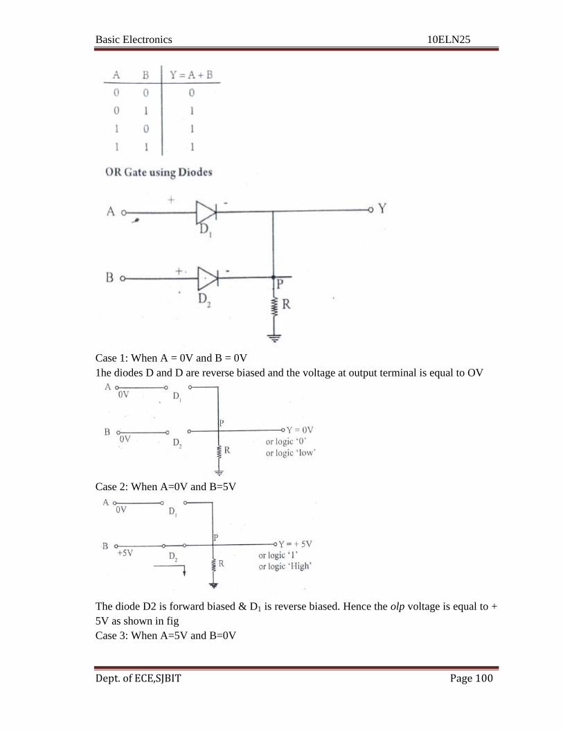
A B
Basic Electronics 10ELN25
Dept. of ECE,SJBIT Page 100
Case 1: When A = 0V and B = 0V
1he diodes D and D are reverse biased and the voltage at output terminal is equal to OV
Case 2: When A=0V and B=5V
The diode D2 is forward biased & D1 is reverse biased. Hence the olp voltage is equal to +
5V as shown in fig
Case 3: When A=5V and B=0V

Basic Electronics 10ELN25
Dept. of ECE,SJBIT Page 101
The diode D1, is forward biased and D2 is reverse biased. Hence output voltage is equal to
+5V
Case 4: When A = +5V and B = +SV
Both the diodes are forward biased and both the input voltages are connected in parallel
and hence olp voltage is equal to +5V

Basic Electronics 10ELN25
Dept. of ECE,SJBIT Page 102
16. Realize a half adder using AND, OR and inverter logic gates. Write the truth
table. (Jan 2013)(6 M)
The half _ adder is a logic circuit which arithmetically adds two bits. The truth - table of a
half -
adder with inputs A and outputs Sum, S and Carry, C is shown in Table.


![Fafl notes [2010] (sjbit)](https://static.fdocuments.us/doc/165x107/55504974b4c905b2788b4ee1/fafl-notes-2010-sjbit.jpg)

![DBMS Notes [2010] (SJBIT)](https://static.fdocuments.us/doc/165x107/55cf96da550346d0338e3a30/dbms-notes-2010-sjbit.jpg)

