Baseline Proposal for CDAUI-8 Chip-to-Chip (c2c) For IEEE...
26
P802.3ck 1 May 2019 106Gbps C2M Simulation Updates (III) For IEEE 802.3ck May, 2019 Mike Li, Hsinho Wu, Masashi Shimanouchi Intel
Transcript of Baseline Proposal for CDAUI-8 Chip-to-Chip (c2c) For IEEE...

P802.3ck 1May 2019
106Gbps C2M Simulation Updates (III)
For IEEE 802.3ck
May, 2019
Mike Li, Hsinho Wu, Masashi Shimanouchi
Intel

P802.3ck 2May 2019
Contents
• Objective and Motivations
• TP1a Device and Link Configuration
• Package Characteristics
• Channel Characteristics
• TP1a Simulations & Results
• Host Package Length Investigation
• Whole Link (Host to Module) and TP1a Performance Investigation
• Summary and Conclusion
P802.3ck 3May 2019
Objective and Motivation• Include more C2M channels in the investigation
• Reference RX architecture– CTLE: Based on ghiasi_3ck_adhoc_01_021319.pdf
– DFE/FFE options: 4-tap DFE
• C2M performance comparisons at TP1a– COM method: COM, VEC, VOE
– Waveform simulation: Eye height, VEC
• Investigate whole link (host to module) performance with various RX EQ capabilities
• Investigate relationship between whole link and associated TP1a performance
• Previous C2M studies was presented in 802.3ck and OIF CEI– “Ethernet 106Gbps Chip-to-Module (C2M) VSR Simulations and Updates”, by Mike Li, Hsinho Wu, Masashi Shimanouchi, Nov, 2018.
(http://www.ieee802.org/3/ck/public/18_11/li_3ck_01_1118.pdf)
– “106Gbps C2M Simulation Updates”, Mike Li, Hsinho Wu, Masashi Shimanouchi, (http://www.ieee802.org/3/ck/public/19_03/li_3ck_01_0319.pdf)

P802.3ck 4May 2019
Part I: • Investigation with a Ref RX having CTLE+ 4 tap DFE, and simulation results of TP1a

P802.3ck 5May 2019
106.25 Gb/s C2M TP1a Link SimulationsLink & Device Configurations
• Data Rate: 106.25 Gbps, PAM-4
• Test Pattern: QPRBS13, 1M Symbols (for waveform simulations)
• Target BER: 10-5
• TX Die
• VOD: 750 mV-pp (TP0a amplitude)
• 20%-80% Rise/Fall Time: 6.16 ps
• TX FIR:
– Configuration: – 5 taps: 3 pre-taps and 1 post-tap
– Pre-tap 1: [-0.3:0.02:0]
– Pre-tap 2: [0:0.02:0.1]
– Pre-tap 3: [-0.04:0.02:0]
– Post-tap1: [-0.1:0.02:0]
• RLM (level mismatch): 0.95
• TX termination: 50 Ω
• TX Capacitance: 130 fF
• Jitter/Noise
▪ DJ: 0.04 UI-pp (dual-Dirac)
▪ RJ: 0.01 UI-rms
▪ Noise: ~8.89mV-rms (SNRTX=32.5dB)
TX/Host Package
• Package model – Length: 15mm and 32mm T-line + 1.8mm PTH
– T-line/PTH parameters: a1=0.0009909, a2= 0.0002772, tau=6.14e-3 ns/mm, ZcT-line=87.5Ω, ZcPTH=92.5Ω
– Cp = 87fF
• Package crosstalk is < -60 dB (by design)
Ref RX
TP1a Test Topology

P802.3ck 6May 2019
106.25 Gb/s C2M TP1a Link SimulationsLink & Device Configuration (cont.)
TP1a Reference RX – Die Termination: 50 ohms – Capacitance: 0 fF– AFE Filter and CTLE
– Parameter scaled from IEEE 802.3cd ref. CTLE
– Baud: 53.125 Gsym/s– fp1 / fp2 / fz1 / fz2 / fzp = Baud ÷ 1/1.8973/
2.8138/40/40– Based on “ghiasi_3ck_adhoc_01_021319.pdf”
– gDC: 0 to -14dB– gDC2: 0 to -3dB– G: 1.0 (constant)
• FFE/DFE: ▪ DFE-only
▪ 4 taps▪ Range:
▪ DFE: First tap: +/-0.5, others: +/-0.2• Jitter/Noise:
▪ Input noise: 8.2e-9 V2/GHz
RX Package: None

P802.3ck 7May 2019
C2M 15mm & 32mm Host Package Model-- using latest trending 802.3ck LR Package Model

P802.3ck 8May 2019
Test Channel SummaryChannel Description
Insertion Loss (dB)@ 26.56 GHz
ICN (mV-rms)*
1 112G_16dB_(QSFPDD+module card)_TX7_L10 14.40 + TX Pkg 0.64
2 112G_16dB_(QSFPDD+module card)_TX7_L23 14.59 + TX Pkg 0.67
3 112G_16dB_(QSFPDD+module card)_TX3_L10 14.67 + TX Pkg 0.62
4 112G_16dB_(QSFPDD+module card)_TX3_L23 14.82 + TX Pkg 0.69
5 112G_16dB_(QSFPDD+module card)_TX7_Asic 14.76 + TX Pkg 1.18
6 112G_16dB_(QSFPDD+module card)_TX3_Asic 15.01 + TX Pkg 1.29
7 mellitz_3ck_01_0518_C2M\mellitz_9dB 8.93 + TX Pkg 1.87
8 mellitz_3ck_01_0518_C2M\mellitz_11dB 11.16 + TX Pkg 1.61
9 mellitz_3ck_01_0518_C2M\mellitz_13dB 13.13 + TX Pkg 1.42
10 tracy_100GEL_02_0118_Long_Barrel_Via\tx5 16.46 + TX Pkg 0.72
11 tracy_100GEL_02_0118_Long_Barrel_Via\tx6 16.09 + TX Pkg 0.74
12 tracy_100GEL_06_0118_Micro_Via\rx5 14.56 + TX Pkg 0.77
13 tracy_100GEL_06_0118_Micro_Via\rx6 14.59 + TX Pkg 0.66
14 ito_3ck_01_0119_\QSFP_buttom_normal 14.99 + TX Pkg 1.03
15 ito_3ck_01_0119_\QSFP_buttom_worst 15.32 + TX Pkg 0.96
16 ito_3ck_01_0119_\QSFP_top_normal 14.24 + TX Pkg 1.10
17 ito_3ck_01_0119_\QSFP_top_worst 14.23 + TX Pkg 1.06
*: Channel files’ fmax is less than fbaud. ICN results are informative.
P802.3ck 9May 2019
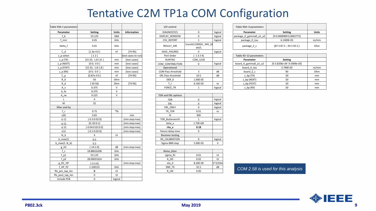
Table 93A-1 parameters I/O control Table 93A–3 parameters
Parameter Setting Units Information DIAGNOSTICS 0 logical Parameter Setting Units
f_b 53.125 GBd DISPLAY_WINDOW 0 logical package_tl_gamma0_a1_a2 [0 0.0009909 0.0002772]
f_min 0.05 GHz CSV_REPORT 1 logical package_tl_tau 6.1400E-03 ns/mm
Delta_f 0.01 GHz RESULT_DIR.\results\100GEL_WG_{d
ate}\package_Z_c [87.5 87.5 ; 92.5 92.5 ] Ohm
C_d [1.3e-4 0 ] nF [TX RX] SAVE_FIGURES 0 logical
z_p select [ 1 2 ] [test cases to run] Port Order [ 1 3 2 4] Table 92–12 parameters
z_p (TX) [15 32; 1.8 1.8 ] mm [test cases] RUNTAG C2M_1218 Parameter Setting
z_p (NEXT) [0 0; 0 0 ] mm [test cases] COM_CONTRIBUTION 0 logical board_tl_gamma0_a1_a2 [0 3.8206e-04 9.5909e-05]
z_p (FEXT) [15 32; 1.8 1.8 ] mm [test cases] Operational board_tl_tau 5.790E-03 ns/mm
z_p (RX) [0 0; 0 0 ] mm [test cases] COM Pass threshold 3 dB board_Z_c 90 Ohm
C_p [0.87e-4 0 ] nF [TX RX] ERL Pass threshold 10.5 dB z_bp (TX) 50 mm
R_0 50 Ohm DER_0 1.00E-05 z_bp (NEXT) 50 mm
R_d [ 50 50] Ohm [TX RX] T_r 6.16E-03 ns z_bp (FEXT) 50 mm
A_v 0.375 V FORCE_TR 1 logical z_bp (RX) 50 mm
A_fe 0.375 V
A_ne 0.525 V TDR and ERL options
L 4 TDR 0 logical
M 32 ERL 0 logical
filter and Eq ERL_ONLY 0 logical
f_r 0.75 *fb TR_TDR 0.01 ns
c(0) 0.65 min N 300
c(-1) [-0.3:0.02:0] [min:step:max] TDR_Butterworth 1 logical
c(-2) [0:.02:0.1] [min:step:max] beta_x 1.70E+09
c(-3) [-0.04:0.02:0.0] [min:step:max] rho_x 0.18
c(1) [-0.1:0.02:0] [min:step:max] fixture delay time 0
N_b 4 UI Receiver testing
b_max(1) 0.5 RX_CALIBRATION 0 logical
b_max(2..N_b) 0.2 Sigma BBN step 5.00E-03 V
g_DC [-14:1:0] dB [min:step:max]
f_z 18.88016206 GHz Noise, jitter
f_p1 53.125 GHz sigma_RJ 0.01 UI
f_p2 28.00031624 GHz A_DD 0.02 UI
g_DC_HP [-3:1:0] [min:step:max] eta_0 8.20E-09 V^2/GHz
f_HP_PZ 1.328125 GHz SNR_TX 32.5 dB
ffe_pre_tap_len 0 UI R_LM 0.95
ffe_post_tap_len 0 UI
Include PCB 0 logical
Tentative C2M TP1a COM Configuration
COM 2.58 is used for this analysis

P802.3ck 10May 2019
CH5 112G_16dB_(QSFPDD+module card)_TX7_Asic Simulationw/ 32mm Host Package
10
CH OutputTX Output RX CTLE output
BER EW (UI) EH (V)
10^-1 0.498 0.0305
10^-2 0.33 0.0237
10^-3 0.252 0.0194
10^-4 0.21 0.0164
10^-5 0.181 0.0138
10^-6 0.157 0.0117
10^-7 0.138 0.00995
10^-8 0.119 0.00855
10^-9 0.103 0.00733
10^-10 0.0869 0.00628
10^-11 0.0732 0.00524
10^-12 0.0605 0.00436
RX FFE outputEH=13.8mV EW=0.18 UI BER=1e-5
P802.3ck 11May 2019
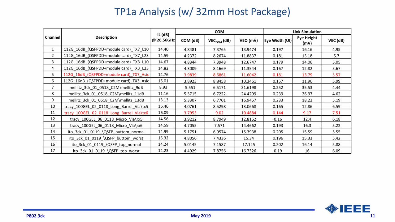
TP1a Analysis (w/ 32mm Host Package)
Channel DescriptionIL (dB)
@ 26.56GHz
COM Link Simulation
COM (dB) VECCOM (dB) VEO (mV) Eye Width (UI)Eye Height
(mV)VEC (dB)
1 112G_16dB_(QSFPDD+module card)_TX7_L10 14.40 4.8481 7.3765 13.9474 0.197 16.16 4.95
2 112G_16dB_(QSFPDD+module card)_TX7_L23 14.59 4.2372 8.2674 11.8837 0.181 13.18 5.7
3 112G_16dB_(QSFPDD+module card)_TX3_L10 14.67 4.8344 7.3948 12.6747 0.179 14.06 5.05
4 112G_16dB_(QSFPDD+module card)_TX3_L23 14.82 4.3009 8.1669 11.3544 0.167 12.82 5.67
5 112G_16dB_(QSFPDD+module card)_TX7_Asic 14.76 3.9839 8.6861 11.6042 0.181 13.79 5.57
6 112G_16dB_(QSFPDD+module card)_TX3_Asic 15.01 3.8923 8.8458 10.3461 0.157 11.96 5.99
7 mellitz_3ck_01_0518_C2M\mellitz_9dB 8.93 5.551 6.5171 31.6198 0.252 35.53 4.44
8 mellitz_3ck_01_0518_C2M\mellitz_11dB 11.16 5.3715 6.7222 24.4299 0.239 26.97 4.62
9 mellitz_3ck_01_0518_C2M\mellitz_13dB 13.13 5.3307 6.7701 16.9457 0.233 18.22 5.19
10 tracy_100GEL_02_0118_Long_Barrel_Via\tx5 16.46 4.0761 8.5298 13.0668 0.165 12.86 6.59
11 tracy_100GEL_02_0118_Long_Barrel_Via\tx6 16.09 3.7953 9.02 10.4884 0.144 9.17 7.51
12 tracy_100GEL_06_0118_Micro_Via\rx5 14.56 3.9212 8.7949 12.8152 0.16 12.4 6.18
13 tracy_100GEL_06_0118_Micro_Via\rx6 14.59 4.7055 7.571 14.4662 0.193 16.3 5.22
14 ito_3ck_01_0119_\QSFP_buttom_normal 14.99 5.1751 6.9574 15.3938 0.205 15.59 5.55
15 ito_3ck_01_0119_\QSFP_buttom_worst 15.32 4.8056 7.4336 15.34 0.196 15.33 5.42
16 ito_3ck_01_0119_\QSFP_top_normal 14.24 5.0145 7.1587 17.125 0.202 16.14 5.88
17 ito_3ck_01_0119_\QSFP_top_worst 14.23 4.4929 7.8756 16.7326 0.19 16 6.09

P802.3ck 12May 2019
TP1a Analysis (w/ 15mm Host Package)
Channel DescriptionIL (dB)
@ 26.56GHz
COM Link Simulation
COM (dB) VEC (dB) VEO (mV) Eye Width (UI)Eye Height
(mV)VEC (dB)
1 112G_16dB_(QSFPDD+module card)_TX7_L10 14.40 4.6638 7.6293 17.4138 0.175 19.79 5.11
2 112G_16dB_(QSFPDD+module card)_TX7_L23 14.59 3.8102 8.9929 11.7285 0.136 15.24 5.52
3 112G_16dB_(QSFPDD+module card)_TX3_L10 14.67 4.326 8.128 15.7245 0.175 18.85 4.92
4 112G_16dB_(QSFPDD+module card)_TX3_L23 14.82 3.8492 8.9225 11.8438 0.13 14.63 5.53
5 112G_16dB_(QSFPDD+module card)_TX7_Asic 14.76 3.4129 9.7645 10.2999 0.112 13.08 5.98
6 112G_16dB_(QSFPDD+module card)_TX3_Asic 15.01 3.5457 9.4949 10.6269 0.105 12.83 5.74
7 mellitz_3ck_01_0518_C2M\mellitz_9dB 8.93 4.6615 7.6326 38.1007 0.203 44.86 4.52
8 mellitz_3ck_01_0518_C2M\mellitz_11dB 11.16 4.4707 7.9085 28.1915 0.224 33.82 5.11
9 mellitz_3ck_01_0518_C2M\mellitz_13dB 13.13 4.7802 7.4682 24.7157 0.225 27.44 5.27
10 tracy_100GEL_02_0118_Long_Barrel_Via\tx5 16.46 4.8185 7.4162 17.6775 0.191 16.76 5.99
11 tracy_100GEL_02_0118_Long_Barrel_Via\tx6 16.09 3.0887 10.4795 11.2993 0.138 14.34 6.2
12 tracy_100GEL_06_0118_Micro_Via\rx5 14.56 3.3786 9.8362 17.421 0.151 17.81 7.39
13 tracy_100GEL_06_0118_Micro_Via\rx6 14.59 4.2958 8.1749 17.9913 0.183 19.99 5.3
14 ito_3ck_01_0119_\QSFP_buttom_normal 14.99 4.8174 7.4176 19.7036 0.208 18.89 5.63
15 ito_3ck_01_0119_\QSFP_buttom_worst 15.32 4.5998 7.7201 20.1922 0.198 18.68 5.8
16 ito_3ck_01_0119_\QSFP_top_normal 14.24 4.1953 8.3345 20.888 0.181 22.93 5.42
17 ito_3ck_01_0119_\QSFP_top_worst 14.23 3.4986 9.5892 16.3775 0.16 18.72 5.88
12

P802.3ck 13May 2019
Results between COM and Waveform Simulation Methods
• Good correlation (~97%) between COM’s VEO and eye heights from waveform simulations– Mean diff ~= 1.61mV, Std. diff ~= 1.91mV
Slope = 1
P802.3ck 14May 2019
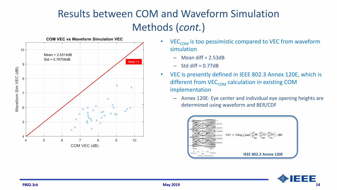
Results between COM and Waveform Simulation Methods (cont.)
• VECCOM is too pessimistic compared to VEC from waveform simulation
– Mean diff = 2.53dB
– Std diff = 0.77dB
• VEC is presently defined in IEEE 802.3 Annex 120E, which is different from VECCOM calculation in existing COM implementation
– Annex 120E: Eye center and individual eye opening heights are determined using waveform and BER/CDF
IEEE 802.3 Annex 120E
Slope = 1

P802.3ck 15May 2019
Host TX Package Length Sweep
• Observations– Channel 5 & 11’s TP1a COM is very close or marginal to 3dB. This indicates that whole link may or will fail to meet COM threshold at target BER
– With the requirement that module RX has to be the same or better EQ as in the baseline RX, baseline RX needs to improve or channel spec. needs to be tightened

P802.3ck 16May 2019
Summary for Part I • Good correlation (~97%) between COM’s VEO and eye heights from waveform simulations
– Mean diff ~= 1.61mV, Std. diff ~= 1.91mV
• VECCOM is too pessimistic compared to VEC from waveform simulation
– Mean diff = 2.53dB
– Std diff = 0.77dB
• Ref RX with CTLE + 4 tap DFE performance over ref package lengths – Some channel TP1a COM is very close or marginal to 3dB. This indicates that whole link may or will fail to meet COM threshold at target BER
– With the requirement that module RX has to be the same or better EQ as in the baseline RX, baseline RX needs to improve or channel spec. needs to be tightened
• To come-up meaningful and self-consistent threshold values for TP1a, corresponding whole link sim is needed.

P802.3ck 17May 2019
Part II: • Investigation with a Ref RX having CTLE+ 4-10 tap DFE, and simulation results of TP1a
and whole-link

P802.3ck 18May 2019
Experiments to find baseline RX based on whole link analysis
• Whole link is constructed by including TP1a channel and module RX package– Sweep module RX DFE tap length from 4 to 12
• Module RX package configuration* – Cd = 100fF
– Cp = 65fF
– Length: 2mm ~ 5mm T-line + 0mm PTH
• T-line/PTH parameters: a1=0.0009909, a2= 0.0002772, tau=6.14e-3 ns/mm, ZcT-line=87.5Ω, ZcPTH=92.5Ω
*: Package info contributed by Piers Dawe <[email protected]>, Ali Ghiasi <[email protected]>, and Edward Frlan <[email protected]>
P802.3ck 19May 2019
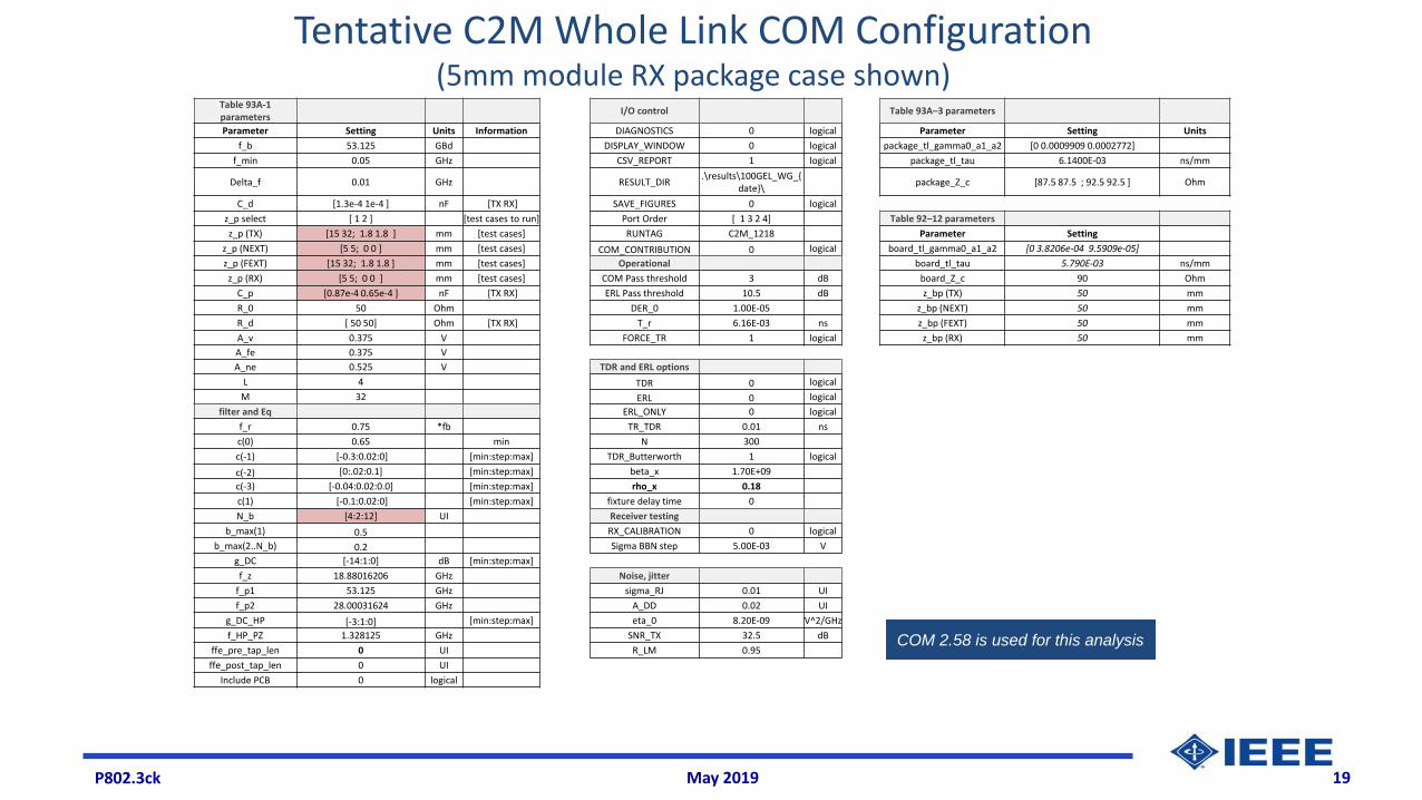
Table 93A-1 parameters
I/O control Table 93A–3 parameters
Parameter Setting Units Information DIAGNOSTICS 0 logical Parameter Setting Units
f_b 53.125 GBd DISPLAY_WINDOW 0 logical package_tl_gamma0_a1_a2 [0 0.0009909 0.0002772]
f_min 0.05 GHz CSV_REPORT 1 logical package_tl_tau 6.1400E-03 ns/mm
Delta_f 0.01 GHz RESULT_DIR.\results\100GEL_WG_{
date}\package_Z_c [87.5 87.5 ; 92.5 92.5 ] Ohm
C_d [1.3e-4 1e-4 ] nF [TX RX] SAVE_FIGURES 0 logical
z_p select [ 1 2 ] [test cases to run] Port Order [ 1 3 2 4] Table 92–12 parameters
z_p (TX) [15 32; 1.8 1.8 ] mm [test cases] RUNTAG C2M_1218 Parameter Setting
z_p (NEXT) [5 5; 0 0 ] mm [test cases] COM_CONTRIBUTION 0 logical board_tl_gamma0_a1_a2 [0 3.8206e-04 9.5909e-05]
z_p (FEXT) [15 32; 1.8 1.8 ] mm [test cases] Operational board_tl_tau 5.790E-03 ns/mm
z_p (RX) [5 5; 0 0 ] mm [test cases] COM Pass threshold 3 dB board_Z_c 90 Ohm
C_p [0.87e-4 0.65e-4 ] nF [TX RX] ERL Pass threshold 10.5 dB z_bp (TX) 50 mm
R_0 50 Ohm DER_0 1.00E-05 z_bp (NEXT) 50 mm
R_d [ 50 50] Ohm [TX RX] T_r 6.16E-03 ns z_bp (FEXT) 50 mm
A_v 0.375 V FORCE_TR 1 logical z_bp (RX) 50 mm
A_fe 0.375 V
A_ne 0.525 V TDR and ERL options
L 4 TDR 0 logical
M 32 ERL 0 logical
filter and Eq ERL_ONLY 0 logical
f_r 0.75 *fb TR_TDR 0.01 ns
c(0) 0.65 min N 300
c(-1) [-0.3:0.02:0] [min:step:max] TDR_Butterworth 1 logical
c(-2) [0:.02:0.1] [min:step:max] beta_x 1.70E+09
c(-3) [-0.04:0.02:0.0] [min:step:max] rho_x 0.18
c(1) [-0.1:0.02:0] [min:step:max] fixture delay time 0
N_b [4:2:12] UI Receiver testing
b_max(1) 0.5 RX_CALIBRATION 0 logical
b_max(2..N_b) 0.2 Sigma BBN step 5.00E-03 V
g_DC [-14:1:0] dB [min:step:max]
f_z 18.88016206 GHz Noise, jitter
f_p1 53.125 GHz sigma_RJ 0.01 UI
f_p2 28.00031624 GHz A_DD 0.02 UI
g_DC_HP [-3:1:0] [min:step:max] eta_0 8.20E-09 V^2/GHz
f_HP_PZ 1.328125 GHz SNR_TX 32.5 dB
ffe_pre_tap_len 0 UI R_LM 0.95
ffe_post_tap_len 0 UI
Include PCB 0 logical
Tentative C2M Whole Link COM Configuration(5mm module RX package case shown)
COM 2.58 is used for this analysis

P802.3ck 20May 2019
Host-to-Module Whole Link COM Analysis Results
Coverage of channels which pass Whole Link (WL) 3dB COM • 10 DFE taps are needed for all 17 channels to pass 3dB COM
– WL Passing Channel = [1:17]
• 8 DFE taps are needed to cover 13 channels – Failing channel 5, 6, 10, 11; WL Passing Channel = [1:4, 7:9, 12:17]
• 6 DFE taps are needed to cover 11 channels– Failing channel 5, 6, 10, 11 13, 17; WL Passing Channel = [1:4, 7:9, 12, 14:16]
• 4 DFE taps are needed to cover 8 channels– Failing channel 2, 4, 5, 6 10, 11 12, 13, 17; WL Passing Channel = [1, 3, 7:9, 14:16]
Minimum COM values of passing channels are ~[3.05, 3, 3, 3.15, 3.21]dB with [4, 6, 8., 10, 12] DFE taps
Host: 32mm / Module: 5mm Host: 32mm / Module: 2mm Host: 15mm / Module: 5mm Host: 15mm / Module: 2mm
CH/Nb 4 6 8 10 12 CH/Nb 4 6 8 10 12 CH/Nb 4 6 8 10 12 CH/Nb 4 6 8 10 12
1 4.01 4.43 4.59 4.69 4.74 1 4.21 4.42 4.55 4.66 4.72 1 3.72 4.11 4.21 4.4 5.86 1 3.89 4.14 4.01 4.44 6.16
2 3.14 3.81 3.94 4.01 4.07 2 3.86 4.3 4.4 4.48 4.55 2 2.82 3.46 3.54 3.68 5.63 2 3.01 3.51 3.58 3.7 5.88
3 3.16 3.97 4.05 4.14 4.16 3 4.12 4.44 4.48 4.54 4.55 3 3.05 3.76 3.8 4.34 6.04 3 3.38 3.75 3.7 4.31 5.99
4 2.63 3.47 3.49 3.53 3.54 4 3.66 4.14 4.15 4.19 4.21 4 2.46 3.35 3.28 3.82 5.83 4 2.96 3.46 3.28 3.94 5.92
5 2.78 3.47 3.62 3.69 3.74 5 3.56 3.99 4.11 4.19 4.25 5 2.48 3.05 3.14 3.34 5.48 5 2.63 3.03 2.85 3.26 5.63
6 2.34 3.13 3.19 3.23 3.21 6 3.44 3.78 3.79 3.83 3.88 6 2.04 2.81 2.84 3.41 5.7 6 2.68 2.94 2.87 3.51 5.77
7 4.11 4.64 4.65 4.65 4.66 7 4.53 4.83 4.83 4.84 4.85 7 3.69 3.93 3.94 4.24 5.7 7 3.84 3.92 3.93 4.28 5.77
8 4.23 4.58 4.73 4.76 4.79 8 4.55 4.75 4.87 4.89 4.89 8 3.79 4.11 4.17 4.59 5.86 8 3.91 4.13 4.16 4.56 5.8
9 4.14 4.63 4.65 4.66 4.7 9 4.48 4.82 4.83 4.85 4.9 9 3.62 4.22 4.22 4.41 5.83 9 4.11 4.49 4.49 4.79 6.21
10 2.24 2.91 2.97 3.15 3.33 10 2.8 3.05 3.09 3.3 3.54 10 2.78 3.34 3.39 3.53 4.09 10 3.19 3.65 3.66 3.79 4.32
11 2.03 3.47 3.77 3.8 3.83 11 2.58 3.66 3.88 3.93 4.02 11 1.51 2.56 2.83 3.28 4.49 11 1.97 3.08 3.41 3.64 4.67
12 2.41 3.79 4.04 4.06 4.06 12 2.49 4.03 4.16 4.19 4.2 12 1.98 3 3.2 3.72 5.04 12 1.97 3.23 3.28 3.75 5.05
13 2.72 3.55 3.82 3.87 3.93 13 2.85 3.52 3.68 3.74 3.76 13 2.32 2.93 3.19 3.59 4.7 13 2.62 3.15 3.31 3.57 4.71
14 3.96 4.38 4.8 4.83 4.87 14 4.33 4.54 4.98 5.02 5.05 14 3.88 4.09 4.46 4.93 5.67 14 4.17 4.27 4.62 5.09 5.9
15 3.26 3.69 4.31 4.36 4.39 15 3.82 4.01 4.64 4.7 4.73 15 3.26 3.49 4.1 4.44 5.11 15 3.77 3.85 4.48 4.83 5.56
16 3.81 4.36 4.49 4.77 4.81 16 4.41 4.65 4.86 5.12 5.18 16 3.35 3.56 3.87 4.81 5.57 16 3.65 3.77 4.04 5.11 5.97
17 3.05 3.6 3.79 4.35 4.41 17 3.7 3.93 4.16 4.79 4.85 17 2.46 2.75 3 4.35 5.03 17 2.92 2.97 3.28 4.72 5.53
Whole Link Passing ChannelWhole Link Failing Channel

P802.3ck 21May 2019
TP1a COM AnalysisTP1a COM
32mm 15mm
CH/Nb 4 6 8 10 12 CH/Nb 4 6 8 10 12
1 4.85 5.06 5.16 5.3 5.38 1 4.66 4.98 4.85 5.35 7.14
2 4.24 4.71 4.77 4.89 4.96 2 3.81 3.95 3.97 4.53 6.89
3 4.83 5.2 5.25 5.32 5.33 3 4.33 4.62 4.67 5.42 7.02
4 4.3 4.83 4.84 4.9 4.92 4 3.85 4.15 4.18 4.77 6.78
5 3.98 4.3 4.37 4.47 4.55 5 3.41 3.33 3.43 4.12 6.55
6 3.89 4.39 4.42 4.47 4.49 6 3.55 3.67 3.7 4.1 6.45
7 5.55 5.75 5.76 5.77 5.78 7 4.66 4.73 4.75 5.18 7.27
8 5.37 5.65 5.8 5.82 5.82 8 4.47 4.88 4.92 5.49 7.23
9 5.33 5.67 5.68 5.71 5.78 9 4.78 5.09 5.1 5.44 7.29
10 4.08 4.41 4.47 4.79 5.1 10 4.82 5.26 5.27 5.47 6.24
11 3.8 4.86 5.13 5.21 5.25 11 3.09 4.1 4.48 4.78 6.23
12 3.92 5.3 5.39 5.43 5.43 12 3.38 4.63 4.69 5.16 6.89
13 4.71 5.07 5.33 5.43 5.43 13 4.3 4.7 4.88 5.28 6.73
14 5.18 5.34 5.86 5.88 5.93 14 4.82 4.99 5.38 6.01 7.04
15 4.81 4.94 5.72 5.78 5.82 15 4.6 4.7 5.37 5.93 6.92
16 5.01 5.23 5.51 5.83 5.9 16 4.2 4.29 4.57 5.87 6.94
17 4.49 4.66 4.96 5.76 5.84 17 3.5 3.5 3.8 5.74 6.79
Whole Link Passing ChannelWhole Link Failing Channel

P802.3ck 22May 2019
Whole Link COM vs TP1a COM
DFE Tap Length
4 6 8 10 12
Min. Whole Link COM (dB) 3.05 3 3 3.15 3.21
Min. TP1a COM (dB) 4.2 3.95 3.8 4.1 4.49
Mean (TP1a-WL, dB) 1.02 0.90 0.96 1.18 1.22
Std (TP1a-WL, dB) 0.22 0.29 0.34 0.29 0.29
Only whole link (WL) passing channels are included in the comparison plot.
P802.3ck 23May 2019
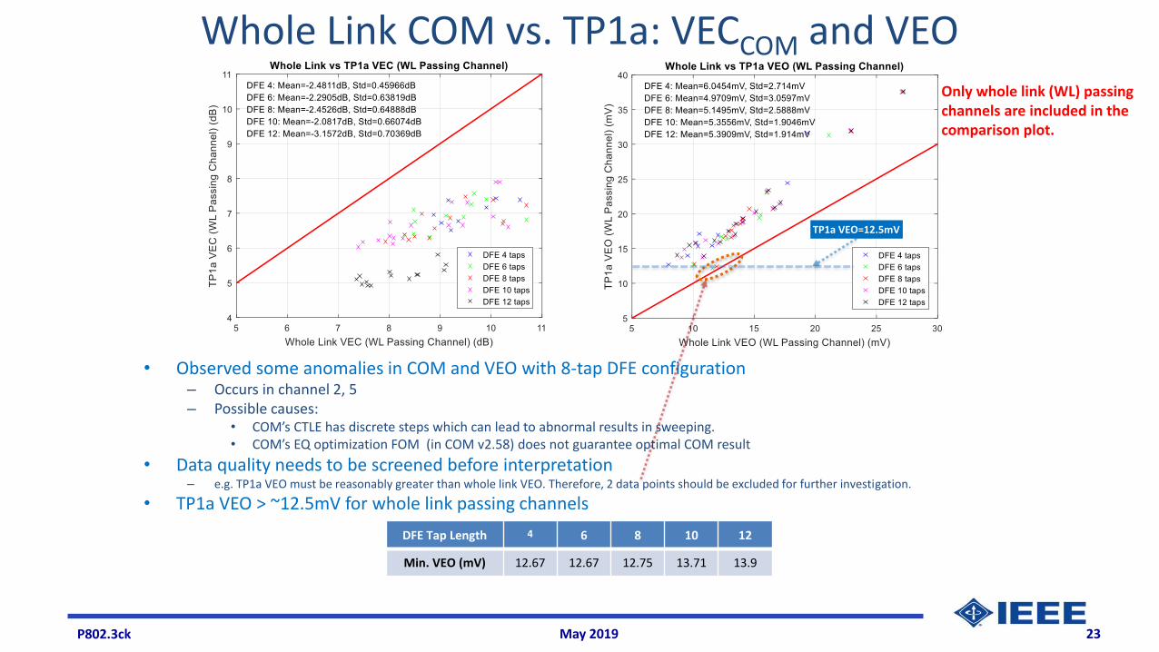
Whole Link COM vs. TP1a: VECCOM and VEO
• Observed some anomalies in COM and VEO with 8-tap DFE configuration– Occurs in channel 2, 5– Possible causes:
• COM’s CTLE has discrete steps which can lead to abnormal results in sweeping.• COM’s EQ optimization FOM (in COM v2.58) does not guarantee optimal COM result
• Data quality needs to be screened before interpretation– e.g. TP1a VEO must be reasonably greater than whole link VEO. Therefore, 2 data points should be excluded for further investigation.
• TP1a VEO > ~12.5mV for whole link passing channels
Only whole link (WL) passing channels are included in the comparison plot.
TP1a VEO=12.5mV
DFE Tap Length 4 6 8 10 12
Min. VEO (mV) 12.67 12.67 12.75 13.71 13.9

P802.3ck 24May 2019
Summary for Part I and II• Evaluated more C2M channels using COM and waveform simulations
– COM’ VEO and eye opening height from waveform simulation correlate reasonably well
– VECCOM (in COM v2.58) differ from waveform simulations’. The gap is about 2.5dB.• COM’s VEC does not literally follow 802.3 Annex 120E definition
• Some channels’ TP1a COM values barely pass 3dB thresholds. Performed whole link (host to module) analysis is necessary and we confirmed that whole link won’t be able to reach 3dB COM at target BER for many test channels.
• Evaluated whole link with extended RX DFE tap length and found:– Need 10 DFE taps to cover all (17) channels
– Need 8 DFE taps to cover 13 channels (~76% channel coverage)
– Need 6 DFE taps to cover 11 channels (~65% channel coverage)
– 4 DFE taps can cover 8 channels (~47% channel coverage)
P802.3ck 25May 2019
Summary for Part I and II cont…• TP1a VEO > 12.5mV (@BER 10-5, 106.25Gbps) for whole link COM passing channels
– 2 channels excluded due to data quality concerns
– Further investigations are needed
P802.3ck 26May 2019
Thank You