Base profile design for high-performance operation of bipolar transistors at liquid-nitrogen...
7
IEEE TRANSACTIONS ON ELECTRON DEVICES, VOL 36. NO 8. AUGUST 1Y8Y 1503 Base Profile Design for High-Performance Operation of Bipolar Transistors at Liquid-Nitrogen Temperature Abstract-The base profile requirements of Si bipolar junction tran- sistors (BJT’s) for high-performance operation at liquid-nitrogen tem- perature are examined. Measurements of thin epitaxial-base polysili- con-emitter n-p-n transistors with increasing base doping show the effects of bandgap narrowing, mobility changes, and carrier freeze- out. At room temperature the collector current at low injection is pro- portional to the integrated base charge, independent of the impurity distribution. At temperatures below 150 K, however, minority injec- tion is dominated by the peak base doping because of the greater effectiveness of bandgap narrowing. When the peak doping in the base approaches lOI9 cm-3, the bandgap difference between emitter and base is sufficiently small that the current gain no longer monotonically de- creases with lower temperature but instead shows a maximum as low as 180 K. The device design window appears limited at the low-current end by increased base-emitter leakage due to tunneling and by resis- tance control at the high-current end. Using the measured dc charac- teristics, circuit delay calculations are made to estimate the perfor- mance of an ECL ring oscillator at room and liquid-nitrogen temperatures. It is shown that if the base doping can be raised to lOI9 cm-3 while keeping the base thickness constant, the minimum delay at liquid nitrogen can approach the delay of optimized devices at room temperature. I. INTRODUCTION OMOJUNCTION bipolar transistors are generally H not considered for operation at liquid-nitrogen tem- peratures because of insufficient dc current gain, increase in base resistance, and degradation of transit time because of lower diffusivity [l]. The reduction in current gain is a result of the smaller bandgap in the emitter than in the base. In thin-base Si transistors, the base current is typically limited by hole injection into the emitter, and therefore its temperature dependence is largely determined by the effective band- gap of the emitter, which is reduced because of heavy doping effects [2]. The collector current, on the other hand, consists of electrons traversing the base, and its temperature dependence is determined by the bandgap in the base. The difference in bandgap between emitter and base causes the ideal gain to decrease exponentially with temperature possibly by two to three orders of magnitude Manuscript received September 16, 1988; revised February 17, 1989. The authors are with the IBM Research Division, Thomas J. Watson Research Center, Yorktown Heights, NY 10598-0218. IEEE Log Number 8928225. between room ( = 300 K) and liquid-nitrogen ( = 80 K) temperatures. In addition to the reduction in current gain ( p), the resistivity of the base region increases sharply because of carrier freeze-out [ 11. Although the net base charge is ef- fectively reduced, which should result in a higher collec- tor current density, the higher base resistance increases the significance of current crowding, which is expected to degrade switching performance. Improvements of low- temperature operation are expected to arise from higher carrier mobilities, such as is the case for MOS devices. Improvements in mobility can be obtained at low base doping levels (10 cm” ~ m - ~ ) , but the device operation will suffer from freeze-out of majority carriers, and the effective mobility for minority carriers is possibly reduced by trapping in the states of a compensating dopant (donor states in an n-p-n) [I]. To avoid these freeze-out effects, the base doping should be raised above the Mott transition (3 X 10” crnp3) [3]. Also, because of the constant volt- age (or current) scaling practiced in bipolar, base doping levels must increase rapidly with smaller dimensions, and improvements in majority carrier mobility, being limited by impurity scattering, cannot be realized [4]. Histori- cally, minority and majority have been assumed identical. Recent data extraction, however [5], indicated that the minority mobility for doping levels above 1 x cm-3 can exceed the majority mobility by a factor of two at room temperature. Contrary to common assumptions, it was reported in 161 that the minority mobility at these high doping levels increases with lower temperature following a power law, as if the minority carriers are screened from impurity scattering. Below 150 K the magnitude of the current is dominated by the number of available minority carriers because of the reduction of kT/q by a factor of two or more. Because transport in the base at high cur- rents is partially by drift and partially by diffusion, the increase of minority mobility with lower temperature has to overcome at least the reduction sion field (2-4 x kT/q) to obtain in the base. DC operation can be optimized enhancement of poly-emitters and lightly doped uncompensated base in the effective diffu- a shorter transit time by utilizing the gain the high mobility of regions [7]. Alterna- 0018-9383/89/0800-1503$01 .OO O 1989 IEEE
Transcript of Base profile design for high-performance operation of bipolar transistors at liquid-nitrogen...

IEEE TRANSACTIONS ON ELECTRON DEVICES, VOL 36. NO 8. AUGUST 1Y8Y 1503
Base Profile Design for High-Performance Operation of Bipolar Transistors at Liquid-Nitrogen
Temperature
Abstract-The base profile requirements of Si bipolar junction t ran- sistors (BJT’s) for high-performance operation at liquid-nitrogen tem- perature a re examined. Measurements of thin epitaxial-base polysili- con-emitter n-p-n transistors with increasing base doping show the effects of bandgap narrowing, mobility changes, and carr ier freeze- out. At room temperature the collector current a t low injection is pro- portional to the integrated base charge, independent of the impurity distribution. At temperatures below 150 K, however, minority injec- tion is dominated by the peak base doping because of the greater effectiveness of bandgap narrowing. When the peak doping in the base approaches l O I 9 cm-3, the bandgap difference between emitter and base is sufficiently small that the current gain no longer monotonically de- creases with lower temperature but instead shows a maximum as low as 180 K. The device design window appears limited at the low-current end by increased base-emitter leakage due to tunneling and by resis- tance control a t the high-current end. Using the measured dc charac- teristics, circuit delay calculations a r e made to estimate the perfor- mance of an ECL ring oscillator at room and liquid-nitrogen temperatures. I t is shown that if the base doping can be raised to l O I 9 cm-3 while keeping the base thickness constant, the minimum delay at liquid nitrogen can approach the delay of optimized devices a t room temperature.
I. INTRODUCTION
OMOJUNCTION bipolar transistors are generally H not considered for operation at liquid-nitrogen tem- peratures because of insufficient dc current gain, increase in base resistance, and degradation of transit time because of lower diffusivity [ l ] .
The reduction in current gain is a result of the smaller bandgap in the emitter than in the base. In thin-base Si transistors, the base current is typically limited by hole injection into the emitter, and therefore its temperature dependence is largely determined by the effective band- gap of the emitter, which is reduced because of heavy doping effects [2]. The collector current, on the other hand, consists of electrons traversing the base, and its temperature dependence is determined by the bandgap in the base. The difference in bandgap between emitter and base causes the ideal gain to decrease exponentially with temperature possibly by two to three orders of magnitude
Manuscript received September 16, 1988; revised February 17, 1989. The authors are with the IBM Research Division, Thomas J . Watson
Research Center, Yorktown Heights, NY 10598-0218. IEEE Log Number 8928225.
between room ( = 300 K ) and liquid-nitrogen ( = 80 K ) temperatures.
In addition to the reduction in current gain ( p ) , the resistivity of the base region increases sharply because of carrier freeze-out [ 11. Although the net base charge is ef- fectively reduced, which should result in a higher collec- tor current density, the higher base resistance increases the significance of current crowding, which is expected to degrade switching performance. Improvements of low- temperature operation are expected to arise from higher carrier mobilities, such as is the case for MOS devices. Improvements in mobility can be obtained at low base doping levels (10 cm” ~ m - ~ ) , but the device operation will suffer from freeze-out of majority carriers, and the effective mobility for minority carriers is possibly reduced by trapping in the states of a compensating dopant (donor states in an n-p-n) [ I ] . To avoid these freeze-out effects, the base doping should be raised above the Mott transition ( 3 X 10” crnp3) [3]. Also, because of the constant volt- age (or current) scaling practiced in bipolar, base doping levels must increase rapidly with smaller dimensions, and improvements in majority carrier mobility, being limited by impurity scattering, cannot be realized [4]. Histori- cally, minority and majority have been assumed identical. Recent data extraction, however [ 5 ] , indicated that the minority mobility for doping levels above 1 x cm-3 can exceed the majority mobility by a factor of two at room temperature. Contrary to common assumptions, it was reported in 161 that the minority mobility at these high doping levels increases with lower temperature following a power law, as if the minority carriers are screened from impurity scattering. Below 150 K the magnitude of the current is dominated by the number of available minority carriers because of the reduction of k T / q by a factor of two or more. Because transport in the base at high cur- rents is partially by drift and partially by diffusion, the increase of minority mobility with lower temperature has to overcome at least the reduction sion field (2-4 x k T / q ) to obtain in the base.
DC operation can be optimized enhancement of poly-emitters and lightly doped uncompensated base
in the effective diffu- a shorter transit time
by utilizing the gain the high mobility of regions [7]. Alterna-
0018-9383/89/0800-1503$01 .OO O 1989 IEEE

I504 IEEE 'IRANSACTIONS ON b.I.ECTRON DEVICES. VOL 36. NO. 8. AUGUST 1989
As-deposited
thickness (nm)
TABLE I B A ~ F PROr lLF C H A R s C l tRISTICC.
As-deposited
doping (em-')
25
80
100
200
Peak Doping
(em-')
1.0 1019 90 3.0 x 10¹⁸
1.0 x 10¹⁹ 150 8.0 x 10l8
1.3 x 10¹⁸ 130 1.0 x 10¹⁸
1.0 x 10'8 225 8.0 1017
tively, the base doping can be raised to reduce the differ- ence in bandgap with the emitter. It has been shown by Tang [SI for the case of p-n-p transistors that a very heav- ily doped base indeed produces devices with functional current gains at liquid nitrogen. Because the latter ap- proach has the potential of high-speed operation at LN temperatures, we have investigated the effect of various base doping profiles with peak doping up to 8 x 1 0 I 8 cm-' in thin-base n-p-n transistors. To allow more independent control of base thickness and doping level, the transistors were fabricated using an epitaxial base as described in the next section. The third section reports on the experimental results and dc device measurements, followed by an as- sessment of the circuit potential of bipolar transistors at liquid-nitrogen temperature in the last section.
11. DEVICE FABRICATION Recent advances in technology have made possible very
shallow, heavily doped base profiles. Rapid annealing has been used to minimize transient enhanced diffusion from implantation [9]. while double diffusion from polysilicon [ I O ] and photo-assisted epitaxy [ 1 1 1 also have been re- ported with successful results. In our devices the base was grown by epitaxy of in-situ boron-doped silicon using UHVICVD technique [ 121. This technology was chosen because it provides uniform base profiles, as confirmed by CV and SIMS. The devices were implemented using the self-aligned-profile concept [ 131. Table I lists the four different base profiles for this study: The peak base dop- ing level varied from 8 x to 8 X 1 0 l 8 cm-', depos- ited at thicknesses ranging from 25 to 200 nm. The final base thickness was verified by SIMS to range from 90 to 250 nm. The emitter was formed using standard LPCVD polysilicon deposition, arsenic ion implantation, and dif- fusion. The emitter drive-in was kept to a minimum, re- sulting in very shallow base-emitter junction depths of 1 5 nm. Further details of the process technology are de- scribed by Harame et al. [14]. Better accuracy at low and medium currents was favored over a limited amount of extra resistance at high current levels because useful high current information can then still be obtained from the current gain characteristics. Extra care was taken to avoid
encroachment of the base-contact profile so that the de- vice characteristics could be attributed to the vertical pro- file only [ 151.
111. EXPERIMENTAL RESULTS The dc characteristics at both room temperature (RT)
and liquid-nitrogen temperature (LN) of two examples of our devices are shown in Figs. 1 and 2 for the most heav- ily doped base ( 8 x 10' ', 150 nm ) and most lightly doped base ( 8 x lo", 225 nm), respectively. Evidently the col- lector current of the 8 x 10" doped base has decreased compared to the 8 x l O I 7 device. The RT data show that the collector current scales with the measured base sheet resistance (Rr lh ) . In fact, as shown in Fig. 3 , a linear re- lationship between J,. and Rdb is obtained at room temper- ature. Apparently the precise impurity distribution for these epitaxial base profiles is not very significant; only the integrated base charge matters. In order to understand this, we rewrite the familiar Gummel expression as
J,. = q2(D,p,,n;e) X Rdh x eqVEElkT ( 1 )
where R,, is the sheet resistance of the pinched base, ni, the effective intrinsic carrier concentration including heavy doping effects, and D, and pp the minority electron diffusivity and majority hole mobility, respectively. At RT the average product of mobilities and intrinsic carrier con- centration over the base is fortuitously constant with dop- ing: as a function of impurity concentration the combined decrease in mobilities for electrons and holes is exactly compensated by the increase in effective intrinsic carrier concentration. Using typical values for the doping depen- dence of the mobilities [16], an effective reduction in bandgap of about 40 meV between 8 x 10'' and 8 X 10" cm-3 peak doping is required to offset the factor of five in mobility decrease. This value compares favorably with published data on the bandgap narrowing dependence on doping [ 171.
This constant proportionality between J , and Rdb is no longer present at LN. This can be seen in Fig. 2, where the collector currents are the same, although the base re- sistance differs by more than an order of magnitude. This is particularly surprising when one anticipates a higher current density from carrier freeze-out and mobility vari- ation for the lightly doped base. In fact, as shown in detail in Fig. 4, essentially no freeze-out was measured for the 8 X 1 0 ' ' case whereas the base resistance of the 8 x 10¹⁷ doped wide-base transistor increased by a factor of five. Fitting the data below 150 K to a single energy activation curve, exp ( E , /2kT ), the corresponding ionization energies (E,) for the lighter doped transistors are in agreement with first-order theory. The more heavily doped samples exhibit a lower activation energy, which can be partly attributed to the broadening of the impurity level into a band and merging with the tail states of the valence band. To first order this reduction is expected to vary with the cube root of the doping level [18]

STORK et al: BASE PROFILE DESIGN FOR OPERATION OF BIPOLAR TRANSISTORS I SOS
0.4 0 6 0.8 1 0 1.2 Base-Emitter Voltage (Volt)
Fig. 1. Gummel plots of transistors with highest and lowest doped base profile at room temperature (298 K ) . The maximum current gains are 19 and 75, respectively. Base sheet resistances are 1.6 and 5.1 kQ/L. re- spectively.
0.4 0.6 0.8 1.0 1.2 Base-Emitter Voltage (Volt)
Fig. 2 . Gummel plots of transistors with highest and lowest doped base profile at liquid-nitrogen temperature (83 K ) . The maximum current gains are 12 and 15. respectively. Base sheet resistances are 2 . 3 and 30 kQ/r. respectively.
60 , I
0 2 4 6 8 1 0 Ease Sheet Resistance (kO/o)
Fig. 3. Collector current versus base sheet resistance R,,,,. A nearly perfect linear relationship is found at room temperature for doping levels up to i oL9 cm-'.
r
2 4 6 8 1 0 1 2 Inverse Absolute Temperature (1000/K)
Fig. 4. Normalized (to RT) base sheet resistance (R , , , ] ) as a function of temperature. Carrier freeze-out is all but absent from the I O " device.
Here, E,,,, is the ionization energy at the low doping limit, N , the acceptor doping in the base, and k a constant. Coni- pensating the impurity de-activation, mobility is expected to increase. Without accounting for the mobility, a com- parison of the data of the 3 X lo i8 and 1 x 10" samples results in the factor k to be 1 5 x l opx eVcm. This is unrealistically high because it would imply a Mott tran- sition at N,, = 7 x 10'' cmp3. Because of uncertainties in profile measurement, the spatial distribution of the do- pants, and measurement of resistance and temperature, we can only be certain that, below 150 K and for doping lev- els between 10l8 and 8 x 10l8, mobility and impurity ef- fects both affect the base resistance.
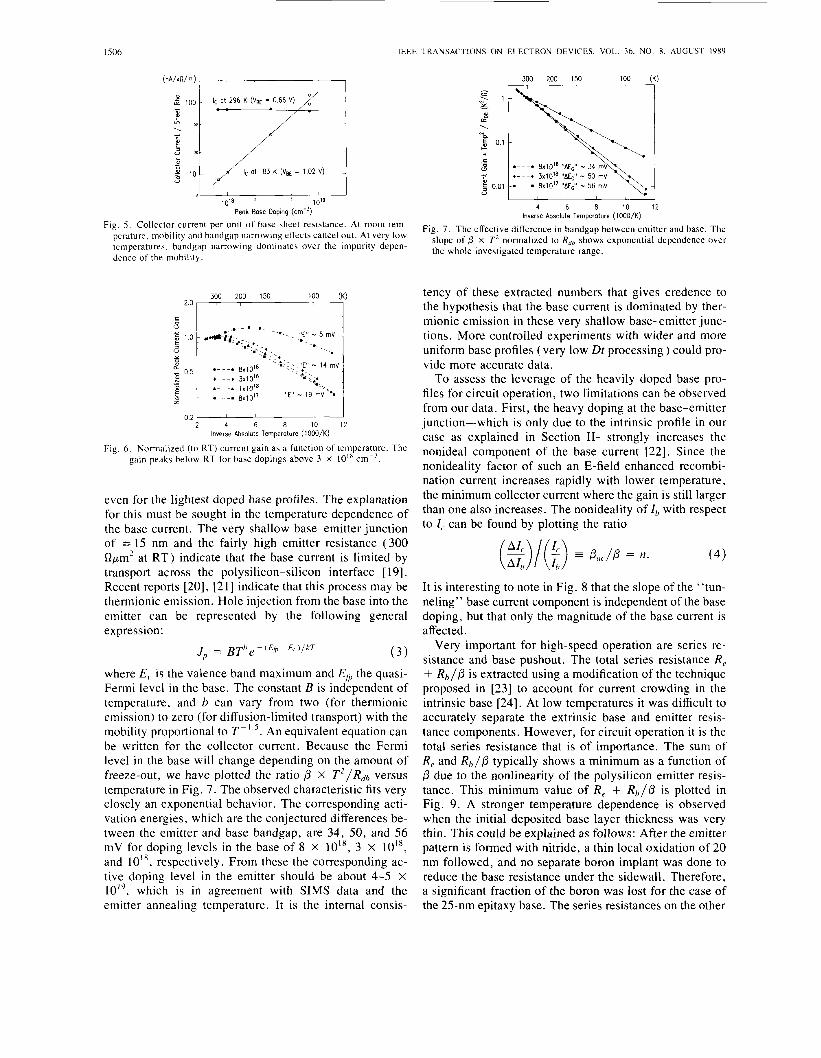
The collector currents at LN were found to be nearly identical for all samples (see again Fig. 2). Referring back to the relationship between J , and R,,,, we realize that future insight in the mobility-intrinsic carrier product can be obtained when the amount of collector current per unit base resistance J,,/R,,,, (not unlike g,,,/& for MOS tran- sistors) is plotted versus the peak base doping level (see Fig. 5 ) at RT and at 83 K . Because of the 4 X reduction in k T / q , bandgap narrowing is much more effective at LN: in other words, mobility variations with doping have a much smaller effect on J,. than the number of carriers available, as determined by the bandgap.
The data in Fig. 5 also allow us to check the tempera- ture dependence of bandgap narrowing. At room temper- ature the doping dependence of bandgap narrowing fol- lows to first order a simple power law, predicting a change of =40 meV per decade of doping. From this and our data it would follow that the product of majority and mi- nority mobilities reduces by a factor of 30 between 8 x lo'' and 8 X 10" at LN. This is significantly more than can be extracted from previous data [4]. On the other hand, assuming the same doping dependence of mobilities at LN as at RT, the corresponding bandgap narrowing is estimated at 30 meV. Therefore, our data seem to support the recent notion of reduced bandgap narrowing at lower temperatures [6].
Since the activation energy of the individual collector and base currents is very much larger than their differ- ence, we have plotted the maximum current gain versus temperature in Fig. 6. The observed differences in 0 ver- sus T in our samples can be attributed to the base profile only, since all wafers underwent identical and simulta- neous emitter processing. As the base doping increases above 1 X 10" cmp3, we notice that the current gain ini- tially increases with lower temperature reaching a maxi- mum at increasingly lower temperature. Because of the small difference in bandgaps between the emitter and base at high doping levels, mobility variations are equally im- portant, in particular above 150 K . The occurrence of car- rier freeze-out below 150 K reduces the apparent activa- tion energy of 0 for the lighter doped devices but only has a minor effect on the 8 x loi8 sample. Unfortunately, with increasing base doping levels, the improvement in mobility is expected to be only a factor of two or less. It is interesting to see that the absolute decrease in 0 is small
1 SO6 l E E t T R A N S A C T I O N S O N ELECTRON DEVICES. VOL. 36. NO. 8. A U G U S T 1989
I I 10'8 1019
Peak Base Doping (cm")
Fig. S . Collector current per unit of base sheet resistance. At room tem- perature, mobility and bandgap narrowing effects cancel out. At very low temperatures. bandgap narrowing dominates over the impurity depen- dence o f the mobility.
300 200 150
2.0 i
0.2 ' 1 I 2 4 6 8 1 0 1 2
lnver~e Absolute Temperature (1000/K)
Fig. 6. Normalized (to RT) current gain as a function of temperature. The gain peaks below RT for base dopings above 3 X I O ' ' cm-j.
even for the lightest doped base profiles. The explanation for this must be sought in the temperature dependence of the base current. The very shallow base-emitter junction of = 15 nm and the fairly high emitter resistance (300 Qpm' at RT) indicate that the base current is limited by transport across the polysilicon-silicon interface [ 191. Recent reports [20], [21] indicate that this process may be thermionic emission. Hole injection from the base into the emitter can be represented by the following general expression:
(3) J p = B T h e - ' E f P - E r d / k T
where E,, is the valence band maximum and Eh the quasi- Fermi level in the base. The constant B is independent of temperature, and b can vary from two (for thermionic emission) to zero (for diffusion-limited transport) with the mobility proportional to T - An equivalent equation can be written for the collector current. Because the Fermi level in the base will change depending on the amount of freeze-out, we have plotted the ratio P X T2/Rdh versus temperature in Fig. 7. The observed characteristic fits very closely an exponential behavior. The corresponding acti- vation energies, which are the conjectured differences be- tween the emitter and base bandgap, are 34, 50, and 56 mV for doping levels in the base of 8 X 10l8, 3 X IO", and lo'', respectively. From these the corresponding ac- tive doping level in the emitter should be about 4-5 X I O J 9 , which is in agreement with SIMS data and the emitter annealing temperature. It is the internal consis-
- 1
Y v
h -.. n a
0.1 t
0 U
c c
5 0.01 U
300 200 150 100 (K)
4 6 8 10 12 Inverse Absolute Temperature (1000/K)
Fig. 7 . The effective difference in bandgap between emitter and base. The slope of fl X T' normalized to Rdh shows exponential dependence over the whole investigated temperature range.
tency of these extracted numbers that gives credence to the hypothesis that the base current is dominated by ther- mionic emission in these very shallow base-emitter junc- tions. More controlled experiments with wider and more uniform base profiles ( very low Dt processing ) could pro- vide more accurate data.
To assess the leverage of the heavily doped base pro- files for circuit operation, two limitations can be observed from our data. First, the heavy doping at the base-emitter junction-which is only due to the intrinsic profile in our case as explained in Section 11-strongly increases the nonideal component of the base current [22]. Since the nonideality factor of such an E-field enhanced recombi- nation current increases rapidly with lower temperature, the minimum collector current where the gain is still larger than one also increases. The nonideality of 1, with respect to I , can be found by plotting the ratio
(4 )
It is interesting to note in Fig. 8 that the slope of the "tun- neling" base current component is independent of the base doping, but that only the magnitude of the base current is affected.
Very important for high-speed operation are series re- sistance and base pushout. The total series resistance R, + Rh/P is extracted using a modification of the technique proposed in [23] to account for current crowding in the intrinsic base [24]. At low temperatures it was difficult to accurately separate the extrinsic base and emitter resis- tance components. However, for circuit operation it is the total series resistance that is of importance. The sum of R, and Rb/P typically shows a minimum as a function of P due to the nonlinearity of the polysilicon emitter resis- tance. This minimum value of R, + Rh/P is plotted in Fig. 9. A stronger temperature dependence is observed when the initial deposited base layer thickness was very thin. This could be explained as follows: After the emitter pattern is formed with nitride, a thin local oxidation of 20 nm followed, and no separate boron implant was done to reduce the base resistance under the sidewall. Therefore, a significant fraction of the boron was lost for the case of the 25-nm epitaxy base. The series resistances on the other

STORK er U / BASE PROFILE DESIGN FOR OPERATION OF BIPOLAR TRANSISTORS 1507
0 250 K @) 128K 0 87 K
3 0 I ' ~ \
10-9 10-6 Collector Current (A)
Fig. 8. The nonideality factor of I), with respect to I, ( 1 1 = A/, / A I / , x //,//, ) . Note that because of tunneling the ideality increases above two. Heavier base doping results in a smaller region of ideal current gain.
300 200 150 100 (K) I1 200 7
.----e 8x10" 80 nm
A---. 1 ~ 1 0 ' ~ 130 nm .' VI
d 100 *
2 4 6 8 1 0 1 2 Inverse Absolute Temperature (1000/K)
Fig. 9. The total series resistance as a function of temperature. A strong increase is only observed on the thin base sample because of dopant loss during oxidation of the l i n k region.
.- . .-.
.---. 8x10'' 80 nm e - - + 3x10" 25 nm
2 4 6 8 1 0 1 2 Inverse Absolute Temperature (1000/K)
Fig. IO. The maximum current density versus temperature. A strong de- crease above room temperature is observed.
wafers is better behaved, but still an increase with lower temperature is observed.
In order to identify the temperature behavior of base pushout, Fig. 10 shows the current at which the current gain peaks. The rapid decrease above RT has a similar temperature dependence as the scattering-limited veloc- ity, but with a much lower "corner" temperature. The higher critical current for the 8 X lo '* base is in quali- tative agreement with the higher maximum electric field at the base-collector junction, which was estimated using numerical simulation. The difference between the two base doping profiles is larger than expected, however, perhaps because of a slight difference in the collector dop- ing.
- , ..
lo-' 10.~ Collector Current (A)
Fig. 1 1 . Gate delay of a lightly loaded ECL ring oscillator: Speed perfor- mance at LN is degraded for base doping levels below 10" cm- '. Higher base doping is required to optimize the devices for low-temperature op- eration. Solid symbols represent room-temperature data; open symbols show liquid-nitrogen data.
10-5 lo-' 10-3 Collector Current (A)
Fig. 12 . Gate delay o f a lightly loaded ECL ring oscillator. With advanced processing a thin base transistor with 0. I - p m base thickness at cm- ', peak doping is possible. Such a device is slower at RT but relatively faster at LN. Solid circles represent rooni-teriiperature~ture data; open squares show liquid-nitrogen temperature data.
IV . PERFORMANCE IMPLICATIONS Using the insight obtained from the measured dc data,
a delay calculation [ 2 5 ] was performed to estimate the speed of ECL ring oscillators. The transit time was cal- culated from the quasi-static charge control expression Qbcl / IL f , where eh(, is the zero-bias base charge, and Ikf is defined as the knee-current where high injection effects start [26]. All parameters are derived from SIMS, dc, and junction capacitance measurements. First a typical RT transistor is compared with the 8 x 10" device of this study. In the case of the heavy doping there is essentially no difference between RT and LN speed, as shown by thc ring-oscillator delay calculations in Fig. 11. As predicted by Dumke [ 11, a degradation in speed occurs for an "op- timum" RT device. On the other hand, because of freeze- out and higher current density, it appears that, with a peak base doping of 8 X l o i 8 c r f 3 and with the same thin base width, speed degradation can be kept within 10 percent of that of RT, as shown in Fig. 12. Note that because of the reduction in k T / q the voltage swing can be reduced theoretically by a factor of four. In our calculations a worst case reduction in voltage swing of 2x was chosen be- cause of various system noise components that are not ex- pected to scale. ' t should be mentioned that the junction capacitances are also slightly lower because of freeze-out. As is the case with MOS, devices are optimized differ- ently for 77 K operation.

1 508 IEEE TRANSACTIONS O N ELECTRON IlF.VICF,S. VOI. 36. SO X. .\LIGIIST 1984
V. CONCLUSIONS Measurements between 400 and 85 K of thin-base n-p-n
transistors with various base dopings showed functional dc characteristics at LN. The current gain no longer de- creased monotonically but peaked at lower temperature as the base doping increased. Below 150 K, however, carrier statistics dominate. It is shown that, because of the elim- ination of freeze-out and the dominant effect of bandgap narrowing, heavily doped thin-base transistors allow fast bipolar circuits at low temperature. The optimized device for liquid-nitrogen operation requires much higher base doping for today’s base thickness. With continued scal- ing, the emerging trend is such that the temperature de- pendence of the bipolar transistor becomes minimal, with little difference between RT and LN operation. However, successful application at LN requires that critical device resistances such as base and emitter contact resistance are sufficiently low.
S. P. Gaur er ( I / . . ”Two-dimensional device simulation program: 2DP.“ IBM J. Res. D ~ v ~ l i ~ p . . v o l . 29. pp. 742-251. May 1985. J . del Alamo, S . Swirhun and R. M. Swanson. “Measuring and niod- eling minority carrier transport in heavily doped silicon.” Solid-Stcite Electron.. vol. 2 8 . pp. 47-54. Jan. 1985. S. S . Li. “The dopant densitj and temperature dependence of hole mobility and resistivity in boron doped silicon.” Solic!-Stutr Elec- tron., vol. 21. pp. 1109-1 117. 1978. G . L. Patton. J . C. Bravnian, and J . D. Plunimer, “Physic\. tech- nology. and modeling of polysilicon emitter contacts for VLSI bipolar transistors.’‘ I € € € Trcrrls. Electrot1 Devic.es, vol. ED-33, pp. 1754- 1768. Nov. 1986. C . C . Ng and E. S . Yang, ”On the temperature characteristics of heavily doped polycrystalline silicon films,” lEDM Tech. Dig.. Dec. 1986. pp. 32-35. E. Crabbe, S . Swirhun, J . del Alamo. R. F. W. Pease. and R. M. Swanson. “Majority and minority carrier transport in polysilicon emitter contacts.“ IEDM Tech. Dig.. Dec. 1986. pp. 28-31. J . C . S . Woo, J . D. Plummer, and J . M. C. Stork. “Non-ideal base current in bipolar transistors at low temperature.“ I € € € T r m s . Elect tron Dr\~icrs, vol. ED-34. pp. 130-138. Jan. 1987. T . H. Ning and D. D. Tang. “Method for determining the emitter
nces of bipolar transistors.” I € € € Trtr,~.\. Elec.rrorl DeviceA. vol. ED-31. pp. 409-412. Apr. 1984. J . M. C . Stork. “Non-ohmic series re\istance of advanced bipolar transistors: Current crowding or poly-emitter resistance’?.” IBM Rcs. Rep., RC 12412. Dec. 1986.
“Bipolar transistor scaling for miniinunl switching dela) and energy dissipation,“ IEDM Tech. Dix . . Dec. 1988. pp. 550-553 .
ACKNOWLEDGMENT Special thanks go to 0. Masrur and c. Palsule for help 1251
[26] I . Getreu. Modeling tl7r Bipdur Trculsisror. Tehtrcnix. Inc.. 1976. with the measurements.
REFERENCES I 1 I W. P. Dumke, “The effect of base doping on the performance of
silicon bipolar transistors at low temperatures.” IEEE Trans. Elec- tron Devices, vol. ED-28, pp. 494-500. May 1981.
[2] R. P. Mertens, R. J . Van Overstraeten. and H. J . De Man, “Heavy doping effects in silicon,” Advances Electronics Electron Phys. , vol. 5 5 , p. 77, 1981.
[ 3 ] N. F . Molt and E. A. Davis, Electronic Processes in Non-crystalline Morerials. New York: Oxford. 1979.
[4] F. J. Morin and J . P. Maita, “Electrical properties of silicon con- taining arsenic and boron,” Phys. Ret) . . vol. 96, pp. 28-35, Oct. 1954.
[SI S . E. Swirhun. “Characterization of majority and minority carrier transport in heavily doped silicon,” Ph.D. dissertation, Sandia Nat. Lab. Jet Prop. Lab.. Electric Power Research Inst., June 1987.
[6] S. E. Swirhun, D. E. Kane, and R. M. Swanson. “Temperature de- pendence of minority electron mobility and bandgap narrowing in P + silicon,” in IEDM Tech. Dig. . Dec. 1988, pp. 298-301.
171 J . C. S . Woo and J . D. Plummer, “Optimization of silicon bipolar transistors for high current gain at low temperatures,” I € € € Trans. Electron Devices, vol. 35, pp. 1311-1321, Aug. 1988.
[8] D. D. Tang, “Heavy doping effects in PNP bipolar transistors.” IEEE Truns. Electron Devices. vol. ED-27, pp. 563-569. Mar. 1980.
[9] H. Takemura et a l . , “Submicron epitaxial layer and RTA technology for extremely high speed bipolar transistors,” in IEDM Tech. Dig.. Dec. 1986, pp. 424-427.
[ I O ] H. K . Park et a l . , “High-speed polysilicon emitter-base bipolar tran- sistor,” IEEE Electron Device Lett., vol. EDL-7. pp. 658-666. Dec. 1986.
[ I I] T . Sugii, T . Yamazaki, T. Fukano, and T . Ito, “Thin-base bipolar technology by low-temperature photo-epitaxy,” in Symp. VLSI Tech- no/. Dig. Tech. Papers, May 1987, pp. 35-36.
1121 T. N. Nguyen, D. L. Harame, J. M. C. Stork, F. K. Le Goues, and B. S . Meyerson, “Characterization of IC devices fabricated in low temperature (550°C) epitaxy by HHVICVD low temperature epi,” in IEDM Tech. Dig.. Dec. 1986. pp. 304-307.
1131 G. P. Li er al. , “Bipolar transistors with self-aligned lateral profile,” I € € € Electron Dellice Lett., vol. EDL-8. pp. 338-340, Aug. 1987.
1141 D. L. Harame, J. M. C . Stork, B. S. Meyerson. T . N. Nguyen. and G. J. Scilla, “Epitaxial-base transistors with ultrahigh vacuum chem- ical vapor deposition (UHVICVD) epitaxy: Enhanced profile control for greater flexibility in device design,” IEEE Elecrron Device Lett., vol. I O , pp. 156-158, Apr. 1989.
[ IS ] D. D. Tang et al. , “Design considerations of high-performance nar- row-emitter bipolar transistors,” I€€€ Electron Device Lett.. vol. EDL-8, pp. 321-323. July 1987.
*
Johannes M. C. Stork (S’79-M‘82) was born i n
Soest. The Netherlands. in 1954. He recci\ed the Ingenieur degree in electrical engineering (cum laude) from Delft University of Technology. Delft, The Netherlands, in 1978 and thc Ph D de- gree from Stanford University. Stanford. CA. in 1982. His dissertation work at Stanford involved the device physics and technology of bipolar stizlctures for VLSI.
During the academic year 1977-1978. he worked at the Philips Research Laboratories.
Briarcliff Manor. NY. on modeling of charge storage in MNOS de! ices. In 1982 he joined the IBM Thomas J . Watson Research Center to work on advanced bipolar technology. In 1985. his interest shifted to the analysis and design of exploratory bipolar devices for high-performance VLSI. and since 1987 he has been Manager of the Exploratory Devices group. His current interest is in the design and application o f hcterojunction devices for silicon technology.
Dr. Stork has been awarded an Outstanding Technical AchieLement Award by IBM. He is a member of the IEEE Electron Devices Society and has served as a member of the VLSI Technology Symposium Program Committee since 1986.
*
David L. Harame (S’77-M‘83) wa\ born i n Po- catello, ID, in 1948. He received the B.A degree in zoology from the University ot Calltornid, Berkeley. in 1971 and the M S degree in zoology from Duke University, Durham. NC. in 1973 He received the M S degree in electrical engineering from San Jose State University. San Jose. CA. in 1976. and the M S degree in material\ \cience and the Ph D degree in electrical engineering. both from Stantord Univer\ity. Stantord, CA. in I986
Since 1986, he ha\ been with the IBM Thomas J Watwn Re\earch Cen- ter in Yorktown Height\. NY. where he is engaged in research on the tab- rication and modeling of bipolar tran\i\tor\ HI \ re\earch interest5 include the fdbricdtion and modeling of epitdXial-baSe silicon bipolar tran\i\tor structure\. SiGe heterojunction bipolar transi\torc. and vertical p-n-p tran- s i stors

STORK er a / : BASE PROFILE DESIGN FOR OPERATION OF BIPOLAR TRANSISTORS I509
Bernard S. 3leyer5on icieiced the Ph D degree in physics from the City College of the City Uni- ver\ity of New York in 1981
Wdtson Re\earch Center d \ a Revarch Staff Member Hi\ earl) work was i n the field ot amor- phou\ \emiconductor\. primarily hydrogenated amorphous carbon films, investigating their elec- tronic properties as related to local atomic order- ing In a broadening of thi\ effort. the trihiological propertie\ ol these layers are being inve\tigated,
and he h d \ organized \everal conference\ focused on wch "diamond-like" carbon layers Recently, hi\ work h'i\ tocu\cd o n the field ot low-temper- ature epitaxy (LTE). demon\trating unique materidl\ and device+ in d nuin- ber ot metastable material system\ ( Si Ge, Si B , and Si Ge B alloy\) At present he mdndges the New Materials and Structures group. m d I F
continuing h i \ \tudie\ i n the held ot heteroepitaxy Dr Meyenon ieceivcd the Young Author9 Award trom the Americdn
A\\ociat ion ot Cry\tal Growth in 1987 tor d e \ c l o p i n ~ the UHViCVD growth technique employed i n h i \ current LTE work
He subwqucnt ly joined the IBM Thoinds J
Thao N. Nguyen (S'80-M'82) received the B.E. degree (honors class I and university medal) in electrical engineering from the University of New South Wales, Sydney, Australia, in 1978 and the M.S. and Ph.D. degrees in electrical engineering from Stanford University in 1980 and 1984. re- spectively. His undergraduate and graduate re- search work involved device physics, modeling. simulation, fabrication, and characterization of power DMOSFET's, CCD's (for ultrasonic ini- aninn). and small-neometrv surface-channel and
buried-channel MOSFET';. I'
He joined the IBM Thomas J . Watson Research Center in 1983 as a Research Staff Member working on exploratory materials and processes for silicon technology. He became Manager of Growth, Interfaces. and Anal- ysis in 1987. His research interests include advanced low-temperature pro- cesses (UHVICVD epitaxy, PECVD insulators. CVD metal) and their ap- plications to ULSI devices, ultra-thin insulator growth and characterization, oxide breakdown and reliability, MOS measurement techniques. and pro- cess-induced defects. He has authored or coauthored about 35 technical papers related to these areas.
Dr. Nguyen is a member of Eta Kappa Nu, Tau Beta Pi, the IEEE Elec- tron Devices Society, the Electrochemical Society. the Material Research Society. and the American Physical Society. He has been awarded an Out- standing Technical Achievement Award and a Research Division Award from IBM.
-