
B01: Digital Clock Report · PDF fileThis report intends to record the conduction process of...
26
B01: Digital Clock Report Author: 1302509 Zhao Ruimin 1300933 Xiong Feng 1302866 Wang Bowen 1302867 Liu Jitong Module: EEE 116 Lecturer: Dr.Du Date: June/4/2015
Transcript of B01: Digital Clock Report · PDF fileThis report intends to record the conduction process of...

B01: Digital Clock Report
Author: 1302509 Zhao Ruimin
1300933 Xiong Feng
1302866 Wang Bowen
1302867 Liu Jitong
Module: EEE 116
Lecturer: Dr.Du
Date: June/4/2015
Abstract
This report intends to record the conduction process of the stopwatch project carried
out in this semester whose experimenters are 4 students. The project requirement was to
build a digital clock circuit that can counter 1 minute on a breadboard using at least two
counters.
The achievement of this project of the group was that a digital clock that included three
counters with additional functions such as buzzer, speeding shifting, and preset functions
was constructed and simulated successfully. the apparatus used were primarily IC chips
such as 74160, 7447 provided by lab and a big breadboard purchased by the group online
(can be seen in Appendix A) to build complex and big circuit that was designed.
One limitation of this project outcome was that the counting down function was failed
to be added to the circuit due to the time constrain. Also, an expected future improvement
of conducting this kind of project was that the circuit out-looking was expected to be more
clear and beautiful if possible. To achieve this, skillful wiring ability and enough wiring
practice are needed.
i

Contents
Abstract i
Contents iii
1 Introduction 1
1.1 Background . . . . . . . . . . . . . . . . . . . . . . . . . . . . . . . . . . . . 1
1.2 Requirement and Apparatus . . . . . . . . . . . . . . . . . . . . . . . . . . . 1
1.3 Objective . . . . . . . . . . . . . . . . . . . . . . . . . . . . . . . . . . . . . 1
2 Methodology 2
2.1 Overall Summary of Circuit . . . . . . . . . . . . . . . . . . . . . . . . . . . 2
2.2 Timer system . . . . . . . . . . . . . . . . . . . . . . . . . . . . . . . . . . . 3
2.2.1 555 timer . . . . . . . . . . . . . . . . . . . . . . . . . . . . . . . . . 4
2.2.2 Timer system . . . . . . . . . . . . . . . . . . . . . . . . . . . . . . . 5
2.3 Counter system . . . . . . . . . . . . . . . . . . . . . . . . . . . . . . . . . . 7
2.3.1 “0.1” bit counter and “1” bit counter . . . . . . . . . . . . . . . . . 7
2.3.2 “10” bit counter . . . . . . . . . . . . . . . . . . . . . . . . . . . . . 8
2.4 7-segment LED display system . . . . . . . . . . . . . . . . . . . . . . . . . 10
2.5 Basic Switch System . . . . . . . . . . . . . . . . . . . . . . . . . . . . . . . 10
2.5.1 Turn On/Off . . . . . . . . . . . . . . . . . . . . . . . . . . . . . . . 11
2.5.2 Reset . . . . . . . . . . . . . . . . . . . . . . . . . . . . . . . . . . . 11
2.5.3 Pause . . . . . . . . . . . . . . . . . . . . . . . . . . . . . . . . . . . 12
2.6 Added Modules . . . . . . . . . . . . . . . . . . . . . . . . . . . . . . . . . . 13
2.6.1 Buzzer . . . . . . . . . . . . . . . . . . . . . . . . . . . . . . . . . . . 13
2.6.2 LED . . . . . . . . . . . . . . . . . . . . . . . . . . . . . . . . . . . . 14
2.6.3 Preset Function . . . . . . . . . . . . . . . . . . . . . . . . . . . . . . 14
2.6.4 Deceleration/Acceleration . . . . . . . . . . . . . . . . . . . . . . . . 15
3 Trouble-shooting 16
3.1 Simulation . . . . . . . . . . . . . . . . . . . . . . . . . . . . . . . . . . . . . 16
3.2 Preset switch . . . . . . . . . . . . . . . . . . . . . . . . . . . . . . . . . . . 16
3.3 7-segment LED display mass . . . . . . . . . . . . . . . . . . . . . . . . . . 16
ii
3.4 Buzzer . . . . . . . . . . . . . . . . . . . . . . . . . . . . . . . . . . . . . . . 17
4 Conclusion 18
4.1 Achievement . . . . . . . . . . . . . . . . . . . . . . . . . . . . . . . . . . . 18
4.1.1 Technical . . . . . . . . . . . . . . . . . . . . . . . . . . . . . . . . . 18
4.1.2 Non-technical . . . . . . . . . . . . . . . . . . . . . . . . . . . . . . . 18
4.2 Limitation . . . . . . . . . . . . . . . . . . . . . . . . . . . . . . . . . . . . . 18
4.2.1 Wiring Proficiency . . . . . . . . . . . . . . . . . . . . . . . . . . . . 18
4.2.2 Time Management . . . . . . . . . . . . . . . . . . . . . . . . . . . . 18
A Real Circuit 19
B Weekly Progress 20
C Contribution Form 21
iii

Section 1
Introduction
1.1 Background
Time, something that exists in everyone’s life, is recorded by clocks all the time in our
daily life. The present widely used counting system for time is decimal base as a result of
the fact that this counting base is the most convenient one for people to count using ten
fingers [1]. To be more precise about the counting system of time, it is commonly known
that one day is divided into 24 hours, one hour is divided into 60 minutes and one minute
is divided into 60 seconds, while this particular project particularly focused on building a
digital clock that can count time for one minute.
1.2 Requirement and Apparatus
This project required the experimenters to design and simulate a circuit for a digital
clock that counts from 1 to 59 seconds with switches to control the circuit by pausing,
resetting or turning on/off it. The clock should be built on a breadboard using electronic
components including IC chips - 74160, 7447, 7404, 7408 etc, 7-segment LED, switches,
and sensors such as buzzer.
1.3 Objective
While in this particular group, it was decided that the clock should have advanced
functionalities as well apart from the required basic functions as follow:
• Added counter: Accuracy degree is set to 0.1 by adding one more counter(74160).
• Sensor (Buzzer): The buzzer rings every half minute (when reaching 29/59 seconds)
• LED Display: A LED brights each time when the 1 second unit bit changes digit.
1

Section 2
Methodology
2.1 Overall Summary of Circuit
The whole complete simulation circuit screenshot is presented in Figure 2.1.
Figure 2.1: Whole Circuit
As can be seen in Figure 2.1, the circuit primarily consists of these modules: timer,
three counters, three decoders and their connected 7-segment LED, a buzzer and its con-
2
nected logic gates, and three switches of pausing/turn-on(off)/reset.
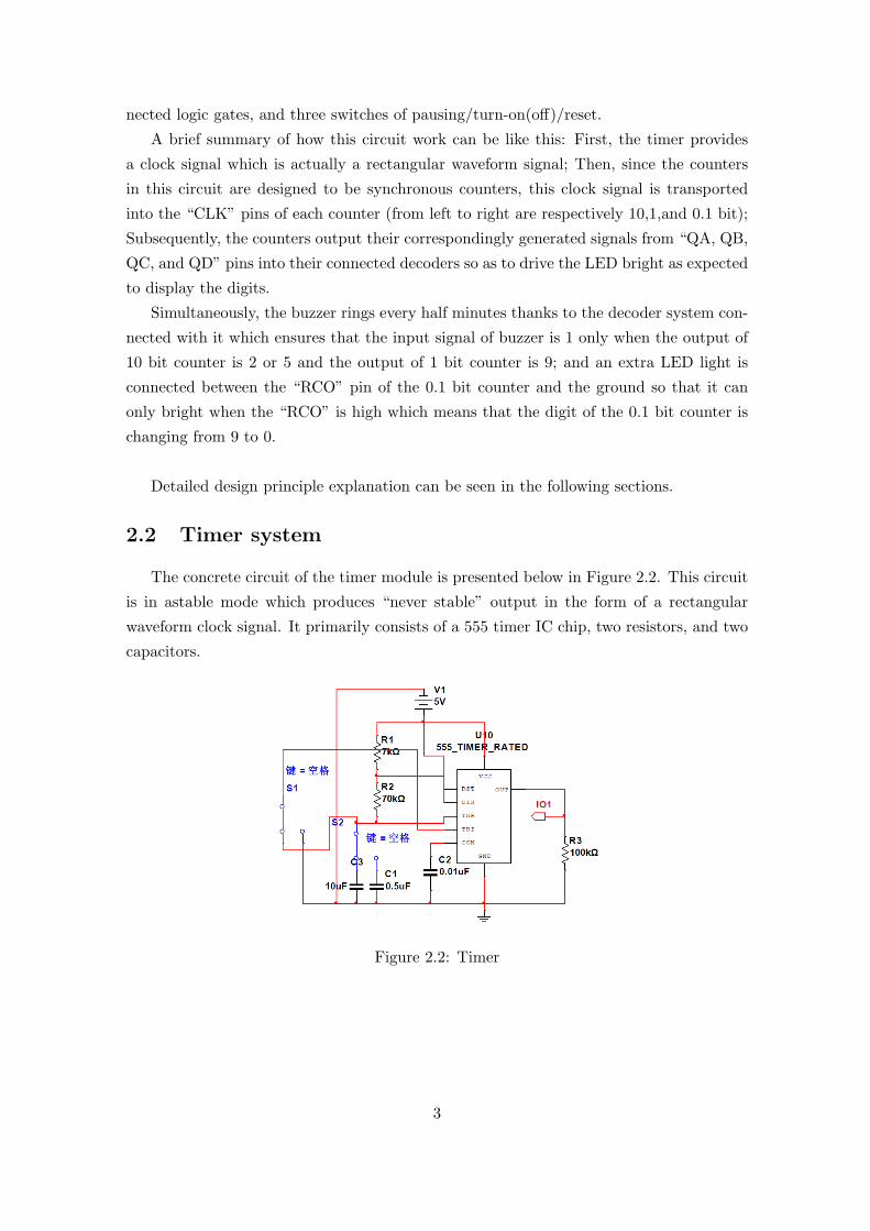
A brief summary of how this circuit work can be like this: First, the timer provides
a clock signal which is actually a rectangular waveform signal; Then, since the counters
in this circuit are designed to be synchronous counters, this clock signal is transported
into the “CLK” pins of each counter (from left to right are respectively 10,1,and 0.1 bit);
Subsequently, the counters output their correspondingly generated signals from “QA, QB,
QC, and QD” pins into their connected decoders so as to drive the LED bright as expected
to display the digits.
Simultaneously, the buzzer rings every half minutes thanks to the decoder system con-
nected with it which ensures that the input signal of buzzer is 1 only when the output of
10 bit counter is 2 or 5 and the output of 1 bit counter is 9; and an extra LED light is
connected between the “RCO” pin of the 0.1 bit counter and the ground so that it can
only bright when the “RCO” is high which means that the digit of the 0.1 bit counter is
changing from 9 to 0.
Detailed design principle explanation can be seen in the following sections.
2.2 Timer system
The concrete circuit of the timer module is presented below in Figure 2.2. This circuit
is in astable mode which produces “never stable” output in the form of a rectangular
waveform clock signal. It primarily consists of a 555 timer IC chip, two resistors, and two
capacitors.
Figure 2.2: Timer
3
2.2.1 555 timer
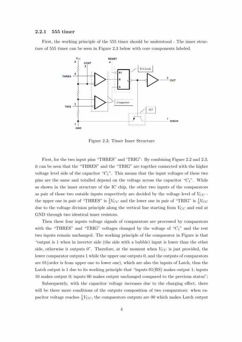
First, the working principle of the 555 timer should be understood - The inner struc-
ture of 555 timer can be seen in Figure 2.3 below with core components labeled.
Figure 2.3: Timer Inner Structure
First, for the two input pins “THRES” and ‘TRIG”: By combining Figure 2.2 and 2.3,
it can be seen that the “THRES” and the “TRIG” are together connected with the higher
voltage level side of the capacitor “C1”. This means that the input voltages of these two
pins are the same and totalled depend on the voltage across the capacitor “C1”. While
as shown in the inner structure of the IC chip, the other two inputs of the comparators
as pair of those two outside inputs respectively are decided by the voltage level of VCC -
the upper one in pair of “THRES” is 23VCC and the lower one in pair of “TRIG” is 1
3VCC
due to the voltage division principle along the vertical line starting from VCC and end at
GND through two identical inner resistors.
Then these four inputs voltage signals of comparators are processed by comparators
with the “THRES” and “TRIG” voltages changed by the voltage of “C1” and the rest
two inputs remain unchanged. The working principle of the comparator in Figure is that
“output is 1 when in inverter side (the side with a bubble) input is lower than the other
side, otherwise it outputs 0”. Therefore, at the moment when VCC is just provided, the
lower comparator outputs 1 while the upper one outputs 0, and the outputs of comparators
are 01(order is from upper one to lower one), which are also the inputs of Latch, thus the
Latch output is 1 due to its working principle that “inputs 01(RS) makes output 1; inputs
10 makes output 0; inputs 00 makes output unchanged compared to the previous status”;
Subsequently, with the capacitor voltage increases due to the charging effect, there
will be three more conditions of the outputs composition of two comparators: when ca-
pacitor voltage reaches 13VCC , the comparators outputs are 00 which makes Latch output
4

unchanged remaining 1;
then when the capacitor voltage reaches 23VCC , the comparators outputs are 10 which
makes Latch output is changed to be 0, and the turned on transistor connects the line
of “DISCH” pin to the ground as shown in Figure 2.2 thus the capacitor starts to be
discharged.
Following that, when the capacitor voltage decreases to 13VCC , the outputs of com-
parators change to 01 again and cause Latch output to be 0 thus turning off the transistor
again to terminate the discharging.
Therefore, a repeated process of charging from 13VCC to 2
3VCC and then discharging
from 23VCC to 1
3VCC of capacitor happens again and again subsequently.
The clear signal relation of all these comparator inputs and outputs, Latch output,
and transistor base voltage are listed in Table 2.1 as shown below.
Table 2.1: Signal Relation
VC1 Upper Comparator Lower Comparator Latch output BJT base volatge notes
0 0 1 1 0one time only0 - 1
3VCC 0 1 1 0
13VCC 0 0 1 0
13VCC - 2
3VCC 0 0 1 0
repeatedprocess
23VCC 1 0 0 1
23VCC - 1
3VCC 0 0 0 1
13VCC 0 1 1 0
Due to the repeated process of the change of these signals, a periodic rectangular
waveform signal is generated through the “OUT” pin.
2.2.2 Timer system
Then combining the 555 timer working principle with the concrete outside circuit,
the design of this whole timer system can be clear. As shown in Figure 2.2, apart from
the already discussed pins “THRES” “TRIG” “DISGH” and “OUT”, there are “VCC”,
“RES”, “GND” and “CON” to discuss.
The “VCC” pin and the “GND” pins are connected to the positive pole providing the
power source for this IC chip and negative pole of the battery respectively;
The “RES” pin is directly connected with a DC power supply. This is because it is a
pin that can force the output of “OUT” to be 0 when it has a input less than 0.7V, thus
it is connected to the high power to avoid this situation from happening;
The “CON” pin is connected to the ground through a capacitor because as a noise
reducer of this circuit and the capacitor is served as a protection of this circuit together;
The two resistors are mainly set to decide the duty cycle of the clock signal based on
the mathematical relationship as shown below where Tm and Ts are the output high time
5

and output low time in one period respectively:
Tm = 0.7× (R1 +R2)× C1 (2.1)
Ts = 0.7×R2 × C1 (2.2)
Here, since Tm ≈ Ts is expected, therefore, the R2 ≫ R1 should be correct, thus, by
reasonable mathematical simplification, the equations were regrouped into:
R2 =0.7
f × C1(2.3)
R1 =R2
10(2.4)
Then, according to these derived formulas, we first chose C1 to be 1µF due to its rich
availability in lab, and the frequency f was set to be 0.1 since the least bit is 0.1 bit.Then
we calculated the corresponding proper resistances of resistors which are R1 = 7kΩ and
R2 = 70kΩ.
The simulation waveform graph in one second (that is ten periods in this case) is
presented below in Figure 2.4 where the red wave is the voltage of capacitor and the green
one is that of the timer output signal.
Figure 2.4: Timer
6

2.3 Counter system
The counter system consists of three counters, that is three 74160 chips. The clock sig-
nal generated by timer is input into the three “CLK” pins of three counters simultaneously.
Each counter has the most simple and basic connection pattern:
• “QA, QB, QC and QD” are outputs that together form 4-bit BCD number.
• “RCO” is 1 only at the moment when the counter reaches 9 and is about to be 0.
• “ENP/T” are two inputs that turn-on the counter only when both of them are 1.
• “CLK” is the input pin that receive the clock signal. “CLR” is a low-active input
pin that can reset the counter back to 0 on it is 0.
• The rest of pins “A,B,C and D” and “LOAD” are pins that are used to set the initial
counting digit.
2.3.1 “0.1” bit counter and “1” bit counter
The counter at the most right position in Figure 2.2 is the “0.1” bit counter; its simu-
lation graph is presented below in Figure 2.5.
Figure 2.5: “0.1” second bit counter
Here for this “0.1” bit counter, the “QA, QB, QC and QD” are connected to corre-
sponding 7447 decoder so that the output BCD can be converted into displayed digits on
LED screen.
The “0.1” bit counter and the “1” bit counter have quite similar connection method
except the fact that for the “1” bit counter, it has one more input than the “0.1” bit
counter - the “ENP” pin of “1” bit counter receive the signal output by the “RCO” pin of
the “0.1” counter. The “RCO” is connected to the “ENP” pin of the left “1” bit counter
so that when the “0.1” bit counter reaches 9 and is about to be 0, the signal 1 provided
by the “RCO” will trigger the “1” bit counter as expected.
7

The counter at the middle position in Figure 2.2 is the “1” bit counter; its simulation
graph is presented below in Figure 2.6.
Figure 2.6: “1” second bit counter
Here for this “1” counter, apart from its mostly similar connection with “0.1” bit
counter and the relation of it with “0.1” bit counter achieved by “RCO” of “0.1” bit
counter and “1” bit counter, it has relation with the most left counter “10” bit counter in
Figure 2.2 - The “RCO” of this “1” bit counter is the input of the “ENP” of the “10” bit
counter. This relation is also to ensure that the left most counter can be triggered when
10 seconds is counted by this “1” bit counter.
2.3.2 “10” bit counter
While the left most counter “10” bit counter has the most distinguishing and complex
connection pattern - it possess logic gates to ensure that it clear itself and restart the
countering when 6 is about to be displayed on its corresponding LED screen.
The counter at the most left position in Figure 2.2 is the “10” bit counter; its simula-
tion graph is presented below in Figure 2.7.
Figure 2.7: “10” second bit counter
8

This counter has slightly different connection structure compared to the other two
counters due to the fact that this counter solely counts from 0 to 5. To enable it to restart
the counting when it reaches 5 and the adjacent lower bit counter reaches 9, a logic gate
system is added: the “QA” and “QB” pins are inputs of a NAND gate and the output of
this NAND gate serves as one input of an AND gate. The other input of this AND gate is
the VCC . The output of this AND gate serves as the input of the “CLR” pin of this “10”
bit counter.
Figure 2.8: The logic gate
As can be seen in Figure above, the logic expression of this logic gate is:
QA×QB × VCC = CLR
In this way, the counter can achieve that when the counter is about to display 6 (0110),
the counter will “clear” itself and restart the counting. And when it restarts the counting,
the counting principle is again similar with that of the “1” bit counter that it change digit
only when it adjacent lower bit counter reaches 9 causing its “RCO” to be 1 thus triggers
its adjacent higher bit counter to change digit due to the input 1 of “ENT” pin.
9

2.4 7-segment LED display system
The core section of this display system is the IC chip 7447. The fundamental structure
of this is a decode that can convert a BCD to a certain 7-pin output. It receives the
outputs of counter 74160 from “QA”, “QB”, “QC” and “QD” pins as its inputs which
together form a BCD. It correspondingly outputs a 7-pin output that matches the BCD.
Apart from these inputs and outputs, there are also three low-active pins on 7447 that
are usually only for pre-test. “display test” pin can enable all the 7 segments to bright
when it receives a low input, “blank input” can enable the directly connected 7-segment
display driver to display a “0” on its screen when given low input, and for the “blank
output” when it is connected to another 7447’s “blank input” and be given a low input,
the another matched 7-segment display driver can be enabled to display a “0”.
Finial, this 7-pin output from the 7447 decode is transported to the 7-segment LED
display driver which is able to light the 7 LED segments accordingly to the 7-pin output.
In this way, the 7-segment LED can display digit from 0 to 9 on the screen accordingly to
the 7447, 74160, timer.
2.5 Basic Switch System
single-pole double-throw switches (SPDT) are used as switches in this project. A con-
ceptual graph of a simple SPDT is presented below.
Figure 2.9: SPDT
The working principle of SPDT is like this: The two parallel row of three pins of the
six-pin SPDT has the same voltage level. Each side of the switch has the same conceptual
structure with the above graph - the middle pin is always connected while the two sides can
be switched to decide which side to be connected with the middle pin and its connected
pathway.
10

2.5.1 Turn On/Off
A SPDT connects power supply with either all the other pins that require power or
the ground serving as the “Turn On/Off” switch.
Figure 2.10: Turn On/Off
This is because when the VCC power supply in connected to the ground rather than the
other pathways that should be connected with power in the circuit, all the power is cut
off in this circuit. In this way, this switch can control whether to provide power to the
while circuit or not thus achieving the functionality of turning on/off the circuit.
2.5.2 Reset
A SPDT connects the trigger pins of “CLR” of three counters with either VCC or the
ground serving as the “reset” switch.
Figure 2.11: Reset
As can be seen in Figure above, for the first two bit counter, the switch is directly connected
with their “CLR” pins. This is easy to understand because the “CLR” is low-active, in
normal condition it should connect high(VCC) but only clear the screen when connected
with low(ground).
11
While for the last bit counter in the left, the VCC input of the AND gate is connected
with the switch. This is because the working principle of “CLR” of that counter is con-
trolled by the logic gate system as discussed previously, and since the switch here serves
as a switch that can cut off this high input of the “CLR” so as to trigger it sometimes,
therefore the connection part is naturally set in the high input pathway.
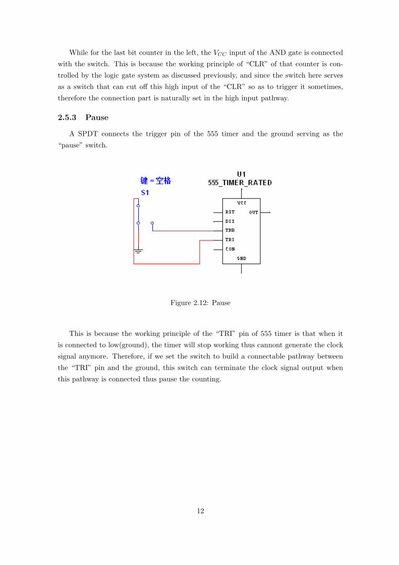
2.5.3 Pause
A SPDT connects the trigger pin of the 555 timer and the ground serving as the
“pause” switch.
Figure 2.12: Pause
This is because the working principle of the “TRI” pin of 555 timer is that when it
is connected to low(ground), the timer will stop working thus cannont generate the clock
signal anymore. Therefore, if we set the switch to build a connectable pathway between
the “TRI” pin and the ground, this switch can terminate the clock signal output when
this pathway is connected thus pause the counting.
12

2.6 Added Modules
2.6.1 Buzzer
A buzzer which can ring every half minutes is connected as shown in Figure below.
Figure 2.13: Buzzer
Due to the decoder which consists of logic gates including inverter, AND gate and
NAND gate, the input signal of buzzer is ensured to be high each time when counter reach
29 or 59(ignore the least bit counter here), and ring for one second. This is because the
decoder ensure that only when the BCD output of the “10 bit counter” is 2 the output of
this decoder can produce a output of 1.
Then, the output of this decoder of “2” and the “RCO” pin of the “1 bit counter”
together serve as the input of one of the two AND gates. While the inputs of the other
AND gate are the “RCO” pin and the output of the AND gate in the most left which
outputs 1 only when “10 bit counter” reaches 5. According to the working principle of
AND gate, it can be understood that these two AND gates will only output 1 when 29
and 59 are reaches respectively.
Finally, the outputs of these two AND gate together go into the OR gate and the
output os this OR gate goes into the buzzer. Due to the working principle of OR gate,
the input of buzzer is 1 either when 29 is reached or 59 is reached. In this way, the buzzer
can ring every half minute.
13

2.6.2 LED
The “RCO” pin of the “0.1 bit counter” is connected with the positive side of a LED,
and the other side of this LED is connected with the ground. This LED display works
quite simply: when this counter reaches 9 and the “RCO” outputs 1, ths LED will bright.
In this way, the LED bright every second with the same frequency of that of the “1
bit counter” change digit on its screen.
2.6.3 Preset Function
A SPDT connects the “LOAD” pin of the counters with either VCC or the ground
serves as the “preset” switch.
Figure 2.14: Preset
First, in this case, the “A” pins of three counters are all connected with VCC which
means that the “preset” number is 111. As shown in Figure above, the switch decides
whether the input of “LOAD” pins are 1 or 0.
Since the “LOAD” pin is low-active and it enables the screen to display the preset
number(111) when it is input with 0, this switch can decide whether to let the preset 111
be displayed on screen.
14

2.6.4 Deceleration/Acceleration
A SPDT connects all the other pins that should be connected with the capacitor with
either capacitor one or capacitor two serves as the “speed-shifting” switch as shown in the
blue circle in Figure below.
Figure 2.15: Speed Shifting
As discussed previously, the capacitance of the capacitor that connected with “DIS”
pin of timer can control the frequency of the clock signal, therefore, by changing the
capacitor, the counting speed of this circuit will change.
In this case, the “speed-shifting” switch can switch from the two available capacitors
with 1µF and 10µF respectively which can result in a counting speed of 1 second or 0.1
second of the fastest counter.
15

Section 3
Trouble-shooting
3.1 Simulation
3.2 Preset switch
For the project, there was a speed-changing function created by different capacitor. A
capacitor that has ten times capacitance of the original capacitor was set next the original
capacitor. Because the speed of digital clock was influenced by the capacitor recharge
time. Ten times of capacitance will let the recharge time become ten times longer. Then
the speed will be ten times slow. Two capacitor were connect by a single-pole double
position switch. The capacitor was chosen by the state of switch. However, there was
a problem that the digital clock will be change during the change of capacitor (adjust
the switch). Only when the switch was stable enough then the digital clock will become
stable. The error should be caused by the unstable switch change he charge of capacitor
so the signal was chaos. However, when stop the input of 555 timer, the capacitor will
not influence the output. Therefore, using the speed changing after pause will solve the
problem. The problem was solved by this wa.
3.3 7-segment LED display mass
There is a little trouble during the experiment. In the timer part, the polarity of one
capacitance was ignored, so that the frequency of output waveform is continually changing.
Also, in the display part, because there are many resistors connected the decoder and the
7-segment LED display, so some of them were connected with other resistors, so that some
resistances changed and the 7-segment LED cannot work normally. In addition, because
the switch is not very suitable for the breadboard, it could cause the voltage become not
stable so that the 7-segment LED could display a wrong number. So it is necessary to
tightly put the switch into the breadboard. Moreover, there were some connected errors
often happened in the process of connecting circuit, once our digit clock was abnormal,
the circuit would be checked firstly, usually the errors would be found directly.
16
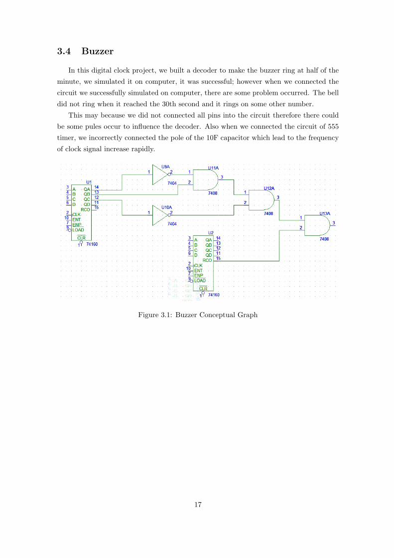
3.4 Buzzer
In this digital clock project, we built a decoder to make the buzzer ring at half of the
minute, we simulated it on computer, it was successful; however when we connected the
circuit we successfully simulated on computer, there are some problem occurred. The bell
did not ring when it reached the 30th second and it rings on some other number.
This may because we did not connected all pins into the circuit therefore there could
be some pules occur to influence the decoder. Also when we connected the circuit of 555
timer, we incorrectly connected the pole of the 10F capacitor which lead to the frequency
of clock signal increase rapidly.
Figure 3.1: Buzzer Conceptual Graph
17

Section 4
Conclusion
4.1 Achievement
4.1.1 Technical
The common used IC chips such as 74160,7447,AND/NAND/NOT gates were utilized
effectively in this experiment. The working principle os these chips were also comprehen-
sively learnt. The circuiting and wiring ability was practiced fully after finish the manual
construction of this stopwatch circuit. The simulation software like multisim and PSpice
were leant and effectively used in this lab to help the design of circuit as well.
4.1.2 Non-technical
The time management skill was practiced in the long-term project. We basically spent
all of our Tuesdays and Wednesdays on the circuit construction section of the project.
Also, the teamwork ability was practiced as well: we worked as a group in the whole
process of this project by dividing the workload and discussing solution and creative ideas
about the circuit design and construction.
4.2 Limitation
4.2.1 Wiring Proficiency
The circuit seems not to have the perfectly clear wiring pattern as can be seen in
Appendix A. This is because we did not really pay enough attention on the out-looking
of the circuit but simply focused on the functions. Therefore, the wires tended to be not
perfectly beautiful. We should have considered the looking at the beginning.
4.2.2 Time Management
We wanted to add the counting down the function to the circuit as well in the process
of the design of the circuit. However, we had to buy extra chips online when the time left
did not allow that purchase delay. We should have planned early about this function and
bought the chips early.
18

Appendix A
Real Circuit
The picture of the real circuit can be seen as below:
Figure A.1: The Circuit
The purchased breadboard can be seen below:
Figure A.2: Purchased Breadboard
19

Appendix B
Weekly Progress
We actually started this project on Week 8 after the mid-term examination and com-
pleted the project on Week 13 until the Deadline. We primarily has these stages of
conducting this project: First, we simulated and constructed the timer system after the
tutorial provided by Dr.Yang directly though with not quite satisfactory efficiency due to
the unskillful practice in terms of the circuiting on breadboard. Then, after refection, we
decided to spend enough time on reading the materials about the working principles of
chips and do the simulation before actually build the circuit for the rest sections. There-
fore, we spent several days in learning the working principles of counters and designed a
successfully simulated circuit with some extra functions first. After the design, we focused
on the circuit construction entirely and after effective teamwork and successful trouble-
shooting process, we conducted a stopwatch circuit with three counters and many extra
functions such as speeding shifting, preset and buzzer.
Figure B.1: Gant Chart
20

Appendix C
Contribution Form
Every group members contributed their own efforts as much as possible by working
together on every Tuesday and Wednesday afternoon for the past few weeks. It is agreed
that all the members have tried their best.
Table C.1: Contribution Form
Member Zhao Ruimin Xiong Feng Wang Bowen Liu Jitong
Percentage 25% 25% 25% 25%
Figure C.1: Signature
21
Reference
[1] “Why is a minute divided into 60 seconds, an hour into 60 min-
utes, yet there are only 24 hours in a day?”. [Online]. Available:
https://www.scientificamerican.com/article/experts-time-division-days-hours-minutes/
22


