
Child Soldiers in Africa The experience of Empowering Hands in Northern Uganda hands.com 1.
1
AX88180 Gigabit Ethernet Controller Application Design Note
AX88180 Gigabit Ethernet Controller Application Design Note
Revision 1.02May 11th, 2010
Copyright (C) 2008 ~ 2010 Reserved by ASIX Electronics Corporation
2
AX88180 Gigabit Ethernet Controller Application Design Note
Copyright (C) 2008 ~ 2010 Reserved by ASIX Electronics Corporation
Revision History
Revision Date Description 1.00 2008/08/15 Initial Release 1.01 2008/09/09 1. Update the reference circuits in Section 2, 3, 4 and 10. 1.02 2010/05/11 1. Added more notes in Section 6, 7, 9.
2. Updated more information of the ESD protection reference circuit in Section 10.
3
AX88180 Gigabit Ethernet Controller Application Design Note
Copyright (C) 2008 ~ 2010 Reserved by ASIX Electronics Corporation
Content 1. .......................................................................................... 5 Introduction2. .................................................... 6 EEPROM Selection Considerations3. ......................................................... 7 Crystal Selection Considerations4. ..................................... 9 Ethernet Magnetic Selection Considerations5. ........................................................................... 11 4-Layer PCB Design6. ....................................... 12 Power and Ground Planes Considerations7. ...................................... 16 Ethernet Magnetic Layout Considerations8. ..................................................................... 18 Thermal Considerations
8-1. .............................................................................. 18 Improve the Cooling Plane8-2. ............................................................................ 18 Improve the Air Convection8-3. .......................................................................... 18 Disable the on-chip regulator
9. ............................................................................ 19 EMI Considerations10. ......................................................................... 21 ESD Considerations
4
AX88180 Gigabit Ethernet Controller Application Design Note
Copyright (C) 2008 ~ 2010 Reserved by ASIX Electronics Corporation
Figures Figure 1. ................................... 7 Clock Source from Gigabit PHY RGMII Interface Reference ConnectionFigure 2. ........................................ 7 Clock Source from Oscillator RGMII Interface Reference ConnectionFigure 3. .......................................................................................... 11 An Example of 4-Layer PCB DesignFigure 4. ................... 12 Typical Chassis/Digital Ground Planes for Single RJ-45 with Integrated MagneticFigure 5. ................................ 12 Typical Chassis/Digital Ground Planes for Separated RJ-45 and MagneticFigure 6. ..................... 13 Typical Digital/Analog Power Planes for Single RJ-45 with Integrated MagneticFigure 7. .................................... 13 Typical Digital/Analog Power Planes for Separate RJ-45 and MagneticFigure 8. ............................... 14 An Example of AX88180 Power Pins and Decoupling Capacitors CircuitsFigure 9. ..................... 16 Gigabit Ethernet MDI0±, MDI1±, MDI2±, and MDI3± Differential Pairs LayoutFigure 10. ......................................................... 18 AX88180 On-Chip Regulator Disabled Reference CircuitFigure 11. .................. 21 An Example of Single RJ-45 Connector Magnetic Circuit for ESD ConsiderationsFigure 12. ......... 22 A Sample ESD Protection Circuit for Single RJ-45 with Integrated Magnetic (Optional)Figure 13. ............................ 23 A Sample ESD Protection Circuit for Separate RJ-45 + Magnetic (Optional)
5
AX88180 Gigabit Ethernet Controller Application Design Note
Copyright (C) 2008 ~ 2010 Reserved by ASIX Electronics Corporation
1. Introduction
ASIX Electronics provides some cost-effective and highly integrated embedded Ethernet controllers that support generic processor interface (local bus interface or Non-PCI) or SRAM-like interface that are commonly used in embedded system applications. The following URL provides detailed online resource of ASIX Electronics single port embedded Ethernet solutions: (Refer to http://www.asix.com.tw/products.php?op=ProductList&PLine=65.)
This Application Design Note applies specifically to the following Gigabit Ethernet controller, namely, AX88180.
AX88180 -- High-Performance Non-PCI 32-bit 10/100/1000M Gigabit Ethernet Controller This Application Design Note provides important information about external component selection, schematic design and PCB design/layout for designing with ASIX Electronics’ embedded Gigabit Ethernet controller. ASIX Electronics highly recommends that user read through this Design Note before starting hardware design on schematic capture and PCB layout.

6
AX88180 Gigabit Ethernet Controller Application Design Note
2. EEPROM Selection Considerations
The following is the EEPROM reference circuit of AX88180 Non-PCI 32-bit 10/100/1000M Gigabit Ethernet application.
Note: 1. The AX88180 supports 16-bit data access serial EEPROM device such as 93C56 EEPROM.
The 93C56 EEPROM is optional if the MAC address can be stored on the Flash memory of your embedded system. The other EEPROM setting can also be configured by AX88180 registers setting.
Copyright (C) 2008 ~ 2010 Reserved by ASIX Electronics Corporation

7
AX88180 Gigabit Ethernet Controller Application Design Note
3. Crystal Selection Considerations
The 125MHz clock sources can be generated from an Oscillator or Gigabit PHY in RGMII mode. Connect to a 125MHz free-running clock source when in RGMII mode. Please refer to the datasheet at the section 5.2 for details about the CLK125 clock, RGMII timing, and related information when implementing this section.
Figure 1. Clock Source from Gigabit PHY RGMII Interface Reference Connection
Figure 2. Clock Source from Oscillator RGMII Interface Reference Connection
Copyright (C) 2008 ~ 2010 Reserved by ASIX Electronics Corporation

8
AX88180 Gigabit Ethernet Controller Application Design Note
The following is the reference 25MHz crystal specification (NSK HC-49/U 25Mhz crystal, with CL 20pF and ESR maximum 40 Ohm) of Marvell 88E1111 Gigabit PHY on the AX88180 + Marvell 88E1111 Gigabit PHY demo board.
Parameter Symbol Typical Value
Nominal Frequency Fo 25.000000MHz Oscillation Mode Fundamental Frequency Tolerance (@25℃) ±30ppm Equivalent Series Resistance ESR 40 Ohm max. Load Capacitance CL 20pF Operation Temperature Range 0℃ ~ +70℃ Aging ±3ppm/year
The following is a sample 25MHz crystal clock circuit of external Gigabit PHY.
Note: Please make sure the XTAL2 25MHz clock output signals are within 25MHz +- 50ppm. If the XTAL2 25Mhz clock output signals are out of the specification, please fine-tune the load capacitors (C47, C48) to meet the specification. The 25MHz clock circuit is dependent on the external PHY. Please refer to the external PHY’s datasheet and reference schematic for the detailed specification requirement of the 25MHz crystal.
Copyright (C) 2008 ~ 2010 Reserved by ASIX Electronics Corporation
9
AX88180 Gigabit Ethernet Controller Application Design Note
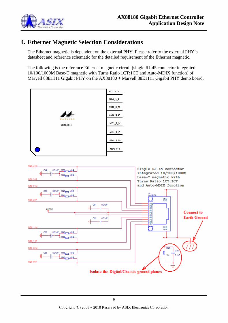
4. Ethernet Magnetic Selection Considerations
The Ethernet magnetic is dependent on the external PHY. Please refer to the external PHY’s datasheet and reference schematic for the detailed requirement of the Ethernet magnetic. The following is the reference Ethernet magnetic circuit (single RJ-45 connector integrated 10/100/1000M Base-T magnetic with Turns Ratio 1CT:1CT and Auto-MDIX function) of Marvell 88E1111 Gigabit PHY on the AX88180 + Marvell 88E1111 Gigabit PHY demo board.
Copyright (C) 2008 ~ 2010 Reserved by ASIX Electronics Corporation

10
AX88180 Gigabit Ethernet Controller Application Design Note
The following is an example (Bothhand LA1S109) of single RJ-45 connector (with integrated 10/100/1000M Base-T magnetic).
Copyright (C) 2008 ~ 2010 Reserved by ASIX Electronics Corporation

11
AX88180 Gigabit Ethernet Controller Application Design Note
Copyright (C) 2008 ~ 2010 Reserved by ASIX Electronics Corporation
5. 4-Layer PCB Design
We strongly suggest customers to design ASIX Electronics’ embedded Gigabit Ethernet controller on the printed circuit board (PCB) with at least 4 layers. The 4-layer PCB design can help reduce some potential EMI, thermal and signal integrity issues, etc. The following is an example 4-Layer PCB design for an embedded system application that uses ASIX Electronics’ embedded Gigabit Ethernet controller.
Layer 1 Component (Top) Magnetic and major signals Layer 2 Ground Digital/analog ground planes Layer 3 Power Digital/analog power planes Layer 4 Component (Bottom) Magnetic and other signals
Figure 3. An Example of 4-Layer PCB Design
12
AX88180 Gigabit Ethernet Controller Application Design Note
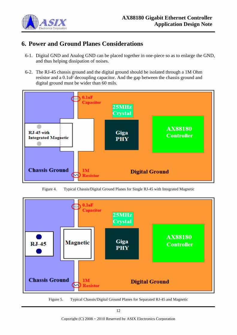
6. Power and Ground Planes Considerations
6-1. Digital GND and Analog GND can be placed together in one-piece so as to enlarge the GND,
and thus helping dissipation of noises.
6-2. The RJ-45 chassis ground and the digital ground should be isolated through a 1M Ohm resistor and a 0.1uF decoupling capacitor. And the gap between the chassis ground and digital ground must be wider than 60 mils.
Figure 4. Typical Chassis/Digital Ground Planes for Single RJ-45 with Integrated Magnetic
Figure 5. Typical Chassis/Digital Ground Planes for Separated RJ-45 and Magnetic
Copyright (C) 2008 ~ 2010 Reserved by ASIX Electronics Corporation
13
AX88180 Gigabit Ethernet Controller Application Design Note
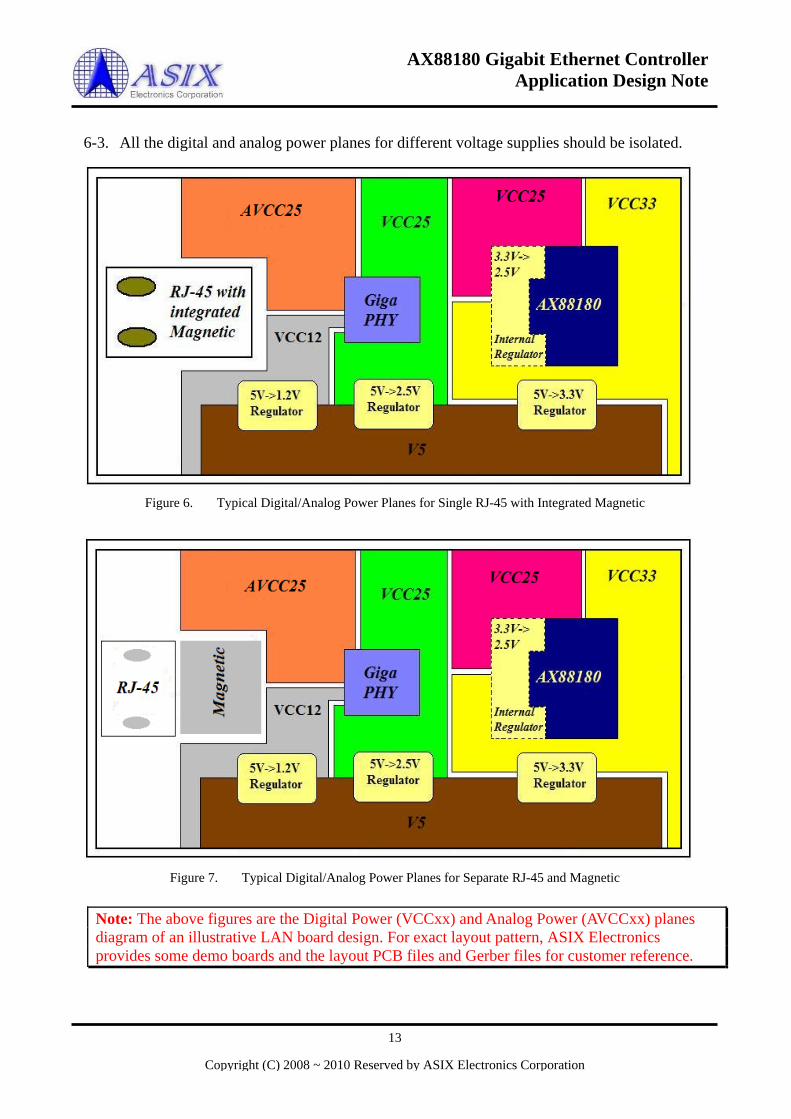
6-3. All the digital and analog power planes for different voltage supplies should be isolated.
Figure 6. Typical Digital/Analog Power Planes for Single RJ-45 with Integrated Magnetic
Figure 7. Typical Digital/Analog Power Planes for Separate RJ-45 and Magnetic
Note: The above figures are the Digital Power (VCCxx) and Analog Power (AVCCxx) planes diagram of an illustrative LAN board design. For exact layout pattern, ASIX Electronics provides some demo boards and the layout PCB files and Gerber files for customer reference.
Copyright (C) 2008 ~ 2010 Reserved by ASIX Electronics Corporation
14
AX88180 Gigabit Ethernet Controller Application Design Note
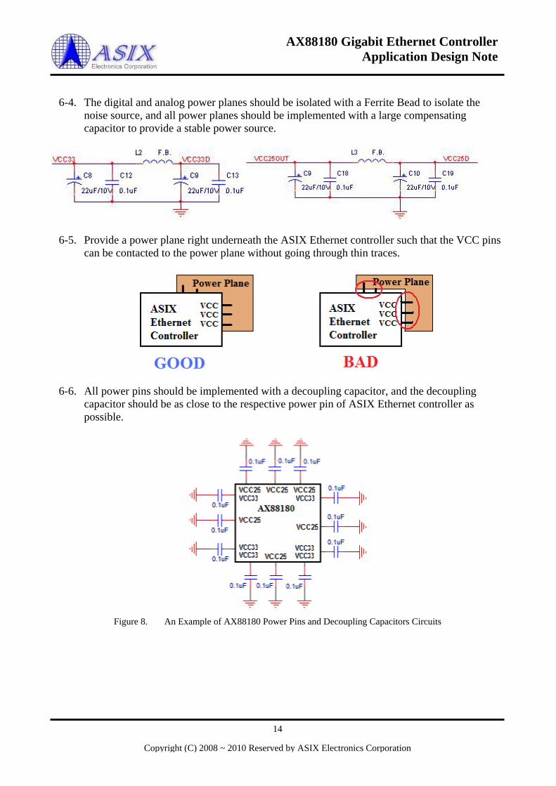
6-4. The digital and analog power planes should be isolated with a Ferrite Bead to isolate the
noise source, and all power planes should be implemented with a large compensating capacitor to provide a stable power source.
6-5. Provide a power plane right underneath the ASIX Ethernet controller such that the VCC pins can be contacted to the power plane without going through thin traces.
6-6. All power pins should be implemented with a decoupling capacitor, and the decoupling capacitor should be as close to the respective power pin of ASIX Ethernet controller as possible.
Figure 8. An Example of AX88180 Power Pins and Decoupling Capacitors Circuits
Copyright (C) 2008 ~ 2010 Reserved by ASIX Electronics Corporation

15
AX88180 Gigabit Ethernet Controller Application Design Note
6-7. The on-chip regulator power input and output traces should be wider than other signal traces
for lower power trace impedance. The power input trace is suggested to be wider than 40 mils and the power output trace is wider than 20 mils. The C8/C9 and C10/C11 compensating capacitors should be as close as the on-chip regulator input/output pins for good power efficiency.
Copyright (C) 2008 ~ 2010 Reserved by ASIX Electronics Corporation

16
AX88180 Gigabit Ethernet Controller Application Design Note
7. Ethernet Magnetic Layout Considerations
The Ethernet magnetic layout considerations are dependent on the external PHY. Please refer to the preferred external PHY Ethernet magnetic layout guide for the detailed requirements.
The following are some general Gigabit Ethernet layout considerations for the differential signals of the Gigabit Ethernet PHY, the Ethernet magnetic and the RJ-45 connector. All trace routes from 10/100/1000M magnetic, RJ-45, and Gigabit Ethernet PHY should be as short as possible. It is an appropriate policy to have the same length for all differential pair signal traces. General speaking, reducing signal crosstalk, providing a solid ground plane, and decreasing parallel route should be considered.
Figure 9. Gigabit Ethernet MDI0±, MDI1±, MDI2±, and MDI3± Differential Pairs Layout
1. The ideal Ethernet differential impedance between the MDI0±, MDI1±, MDI2±, and MDI3±
traces (between MDI0+ and MDI0-, MDI1+ and MDI1-, MDI2+ and MDI2, MDI3+ and MDI3-) should be 100 Ohm. The Ethernet differential impedance between the MDI0+/ MDI0-/ MDI1+/ MDI1- MDI2+/ MDI2/ MDI3+/ MDI3- trace and GND should be 50 Ohm respectively. The designer can use the trace width of MDI0+/ MDI0-/ MDI1+/ MDI1- MDI2+/ MDI2/ MDI3+/ MDI3- traces to fine tune the Ethernet differential impedance value (a wider trace has a smaller impedance value). If the PCB manufacturer provides TDR measurement, it helps control the PCB Impedance.
2. The crystal/oscillator clock source and the switching noises from digital signals should be kept
away from the MDI0±, MDI1±, MDI2±, and MDI3± differential pairs. Moreover, the crystal/oscillator may be sensitive to wander capacitances and noise from other signals; it is better to deploy the crystal far away from I/O ports, high frequency signal traces, magnetic, board edges, and so on.
Copyright (C) 2008 ~ 2010 Reserved by ASIX Electronics Corporation

17
AX88180 Gigabit Ethernet Controller Application Design Note
3. The Ethernet magnetic should be placed as close to the RJ-45 connector as possible. 4. The Gigabit Ethernet PHY should be placed as close as possible to the magnetic. If there are
some limitations on the PCB layout, the trace length from the Gigabit Ethernet PHY to the magnetic should not be longer than 5 inches.
5. The MDI0±, MDI1±, MDI2±, and MDI3± differential pairs should be routed as close as possible. The trace spacing D1 between MDI0+ and MDI0- (or between MDI1+ and MDI1-, MDI2+ and MDI2-, MDI3+ and MDI3-) pair should be in 6 ~ 8 mils. The trace width should be adjusted accordingly to yield the required trace impedance.
6. The spacing D2 should be larger than 200 mils. If the PCB layout is really difficult to meet this requirement, the D2 spacing should be as larger as possible.
7. Route the MDI0±, MDI1±, MDI2±, and MDI3± differential pairs as straight as possible and keep them in parallel for differential pairs.
8. Keep the trace length difference between MDI0+ and MDI0- (or between MDI1+ and MDI1-, MDI2+ and MDI2-, MDI3+ and MDI3-) pair within 700 mils.
9. The termination resistors 49.9Ω and capacitors of the MDI0±, MDI1±, MDI2± and MDI3± differential pairs should be placed as close to the magnetic as possible and the trace should be shorter than 400 mils.
10. Route the MDI0±, MDI1±, MDI2±, and MDI3± differential pairs running symmetric, equal length and close whenever possible.
11. Avoid using vias on the traces of the MDI0±, MDI1±, MDI2±, and MDI3± differential pairs. If the PCB layout really needs to use vias on the differential pairs, please match the vias to keep the differential pairs balanced.
12. The power plane and digital ground plane should not be placed under the magnetic and RJ-45 connector.
13. Avoid routing the signal trace with right angle, instead, the signal trace should be routed with multiple 135° angles.
Worst Better
Copyright (C) 2008 ~ 2010 Reserved by ASIX Electronics Corporation

18
AX88180 Gigabit Ethernet Controller Application Design Note
8. Thermal Considerations
This section describes some information about how to reduce the operating temperature on the embedded Ethernet applications.
8-1. Improve the Cooling Plane
There are some major heat sources on the embedded Ethernet applications included the AX88180 Gigabit Ethernet controller, the external PHY and the external voltage regulators.
You can connect the VCC/GND pins of the AX88180 Gigabit Ethernet controller and the external PHY with wide traces to the respective power/ground planes to increase the cooling effect and reduce the operating temperatures of the AX88180 Gigabit Ethernet controller and external PHY.
You can also add cooling planes on the external voltage regulators to reduce the operating temperature of the external voltage regulators.
8-2. Improve the Air Convection
If the AX88180 Gigabit Ethernet controller and external PHY are implemented on the embedded system, you can place the AX88180 Gigabit Ethernet controller and external PHY at the location with good air convection and stay away from the high-operating-temperature IC such as voltage regulators or MCU to reduce the operating temperature of the AX88180 Gigabit Ethernet controller and external PHY.
8-3. Disable the on-chip regulator
Disabling the on-chip regulator of the AX88180 Gigabit Ethernet controller is an alternative solution to reduce the operating temperature of the AX88180 Gigabit Ethernet controller itself. However, this solution may or may not improve the operating temperature of your overall Gigabit Ethernet applications, depending on how the actual 2.5V power supply is generated.
Figure 10. AX88180 On-Chip Regulator Disabled Reference Circuit
Copyright (C) 2008 ~ 2010 Reserved by ASIX Electronics Corporation

19
AX88180 Gigabit Ethernet Controller Application Design Note
9. EMI Considerations
9-1. The high frequency signals traces such as Ethernet differential signals, clock signals, etc.
shall be surrounded by GND to prevent interference to other signal wires. Better EMI effect can be attained by a one-piece GND underneath the IC furnished with PTH holes to enlarge the GND area.
9-2. The chosen connector must be shielded so that EMI integrity of the design is not compromised. The shield must be electrically connected to chassis ground to extend the chassis barrier for high frequency emissions. If an unshielded connector were used, the EMI would pass through the nylon material of the connector. The shield will also prevent less external EMI from entering the chassis.
9-3. To reduce electromagnetic emissions and susceptibility, it is imperative that traces from the
transceiver to the magnetic sand from the magnetic to the RJ-45 be routed as differential pairs. The objective is to close the loop area formed by the two conductors. The radiated field from the loop or the voltage picked up by the loop by external fields is governed by the field strength and the area formed by the two conductors. Reasonable board design uses 5~10 mils trace widths separated by 10 mils. Transmit differential pairs should be routed adjacent to a VDDO power plane.
9-4. DON’T CROSS ANY SIGNAL TRACES OVER ANY REFERENCE PLANE CUTS.
This might cause some unpredictable EMI problems.
Copyright (C) 2008 ~ 2010 Reserved by ASIX Electronics Corporation

20
AX88180 Gigabit Ethernet Controller Application Design Note
9-5. A clock circuit or high-speed data access may cause an amount of electromagnetic
interference. To minimize noise, EMI, and Jitter, make sure you have installed the termination resistors on the transmitter side (i.e. 22Ω for the MDC, TXD[3:0], TXEN, and TXCX of AX88180). And these resistors must be as close as possible to the AX88180 Gigabit Ethernet controller. To prevent improper PCB trace delays or some external PHYs that may not contain an internal delay element, please reserve 0Ω terminal resistor in the external PHY side for calibrating the impedance to meet the timing between the MAC and PHY interface. Those reserved 0Ω terminal resistors should be also as close as possible to PHY. Theoretically, that could fine-tune and suppress EMI and Jitter if necessary without revising your circuit by doing so.
Copyright (C) 2008 ~ 2010 Reserved by ASIX Electronics Corporation
21
AX88180 Gigabit Ethernet Controller Application Design Note
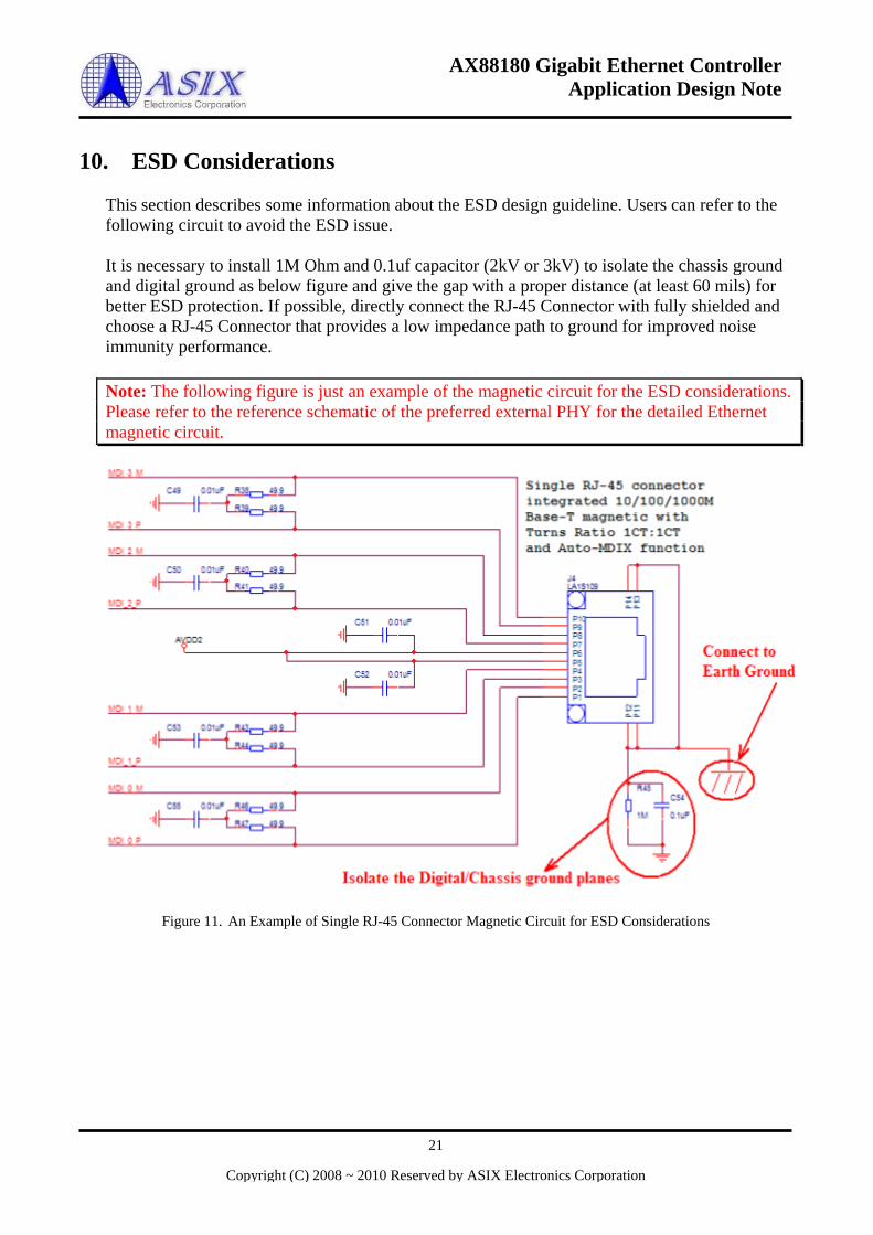
10. ESD Considerations
This section describes some information about the ESD design guideline. Users can refer to the following circuit to avoid the ESD issue.
It is necessary to install 1M Ohm and 0.1uf capacitor (2kV or 3kV) to isolate the chassis ground and digital ground as below figure and give the gap with a proper distance (at least 60 mils) for better ESD protection. If possible, directly connect the RJ-45 Connector with fully shielded and choose a RJ-45 Connector that provides a low impedance path to ground for improved noise immunity performance. Note: The following figure is just an example of the magnetic circuit for the ESD considerations. Please refer to the reference schematic of the preferred external PHY for the detailed Ethernet magnetic circuit.
Figure 11. An Example of Single RJ-45 Connector Magnetic Circuit for ESD Considerations
Copyright (C) 2008 ~ 2010 Reserved by ASIX Electronics Corporation
22
AX88180 Gigabit Ethernet Controller Application Design Note
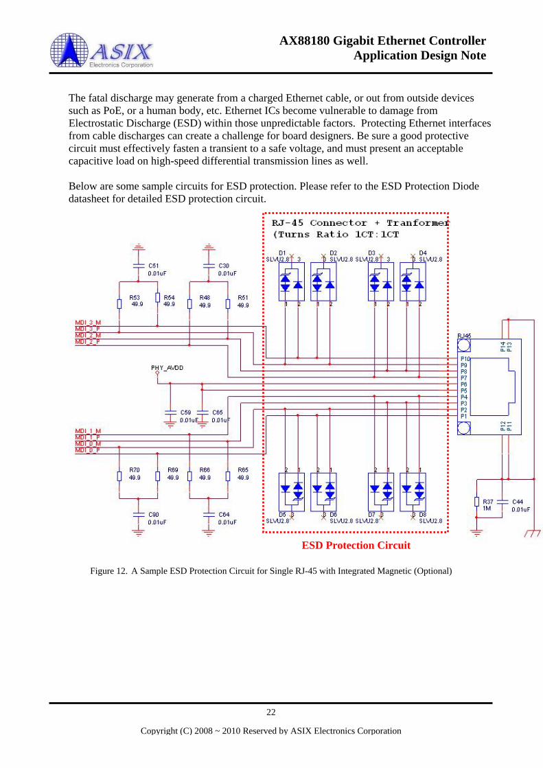
The fatal discharge may generate from a charged Ethernet cable, or out from outside devices such as PoE, or a human body, etc. Ethernet ICs become vulnerable to damage from Electrostatic Discharge (ESD) within those unpredictable factors. Protecting Ethernet interfaces from cable discharges can create a challenge for board designers. Be sure a good protective circuit must effectively fasten a transient to a safe voltage, and must present an acceptable capacitive load on high-speed differential transmission lines as well. Below are some sample circuits for ESD protection. Please refer to the ESD Protection Diode datasheet for detailed ESD protection circuit.
ESD Protection Circuit
Figure 12. A Sample ESD Protection Circuit for Single RJ-45 with Integrated Magnetic (Optional)
Copyright (C) 2008 ~ 2010 Reserved by ASIX Electronics Corporation
23
AX88180 Gigabit Ethernet Controller Application Design Note
ESD Protection Circuit
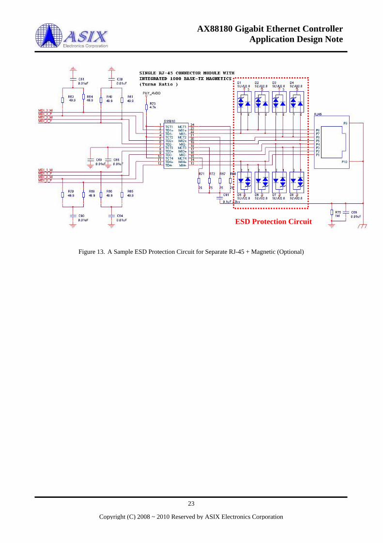
Figure 13. A Sample ESD Protection Circuit for Separate RJ-45 + Magnetic (Optional)
Copyright (C) 2008 ~ 2010 Reserved by ASIX Electronics Corporation

24
AX88180 Gigabit Ethernet Controller Application Design Note
4F, No.8, Hsin Ann RD., Hsinchu Science Park, Hsinchu, Taiwan, R.O.C.
TEL: +886-3-5799500 FAX: +886-3-5799558
Email: [email protected] Web: http://www.asix.com.tw
Copyright (C) 2008 ~ 2010 Reserved by ASIX Electronics Corporation