AvnET EmBEddEd SpEcificATion. · manual. Furthermore, Bluegiga Technologies reserves the right to...
56
Avnet Embedded. Support Around The Board ™ www.avnet-embedded.eu AvnET EmBEddEd SpEcificATion. datasheet Bluegiga WT21
Transcript of AvnET EmBEddEd SpEcificATion. · manual. Furthermore, Bluegiga Technologies reserves the right to...
Avnet Embedded. Support Around The Board™
www.avnet-embedded.eu
AvnET EmBEddEd SpEcificATion.
datasheetBluegiga
WT21

WT21 DATA SHEET
Wednesday, 10 March 2010
Version 1.74

Bluegiga Technologies Oy
Copyright © 2000-2010 Bluegiga Technologies All rights reserved.
Bluegiga Technologies assumes no responsibility for any errors which may appear in this manual. Furthermore, Bluegiga Technologies reserves the right to alter the hardware, software, and/or specifications detailed here at any time without notice and does not make any commitment to update the information contained here. Bluegiga’s products are not authorized for use as critical components in life support devices or systems.
The WRAP is a registered trademark of Bluegiga Technologies
The Bluetooth trademark is owned by the Bluetooth SIG Inc., USA and is licensed to Bluegiga Technologies. All other trademarks listed herein are owned by their respective owners.
Bluegiga Technologies Oy
VERSION HISTORY
Version Comment
0.1 First draft
0.2 Block diagram, descriptions added
0.3 Preliminary version
0.4 Fixed ordering codes added captions
0.5 Power control and regulation info added. Layout guide updated. Minor updates and fixes.
1.0 Electrical characteristic added. Some minor updates.
1.1 Function of the regulator enable pin corrected. Some minor updates.
1.2 New template
1.3 Pinout fixed (GND pins 1 – 3 removed, pin 23 grounded). Layout guide updated.
1.4 Improved dimensions chapter
1.41 Table 5 fixed (pad types)
1.5 Footprint added
1.6 Footprint fixed. Pin number 3 (NC) added.
1.7 Recommended PCB land pattern for WT21-N added, power control and regulation updated. Certification information added
1.71 Information about qualified antenna types added
1.72 Minor updates to chapter 14.5
1.73 Physical dimensions corrected
1.74 UART directions clarified to table 5
Bluegiga Technologies Oy
TABLE OF CONTENTS 1 Ordering Information ................................................................................................. 8 2 Pinout and Terminal Description .................................................................................. 9 3 Microcontroller, Memory and Baseband Logic .............................................................. 12
3.1 AuriStream CODEC ............................................................................................. 12 3.1.1 AuriStream CODEC Requirements ................................................................... 13 3.1.2 AuriStream Hierarchy .................................................................................... 13
3.2 Memory Managements Unit ................................................................................. 14 3.3 Burst Mode Controller ......................................................................................... 14 3.4 Physical Layer Hardware Engine DSP .................................................................... 14 3.5 WLAN Coexistence ............................................................................................. 15 3.6 Configurable I/O Parallel Ports ............................................................................. 15
4 Clock Generation ..................................................................................................... 16 4.1 32kHz External Reference Clock ........................................................................... 16
5 Serial Peripheral Interface (SPI) ................................................................................ 17 5.1 WT21 Serial Peripheral Interface (SPI) .................................................................. 17 5.2 Instruction Cycle ................................................................................................ 17
5.2.1 Writing to the Device .................................................................................... 17 5.2.2 Reading from the Device ............................................................................... 18 5.2.3 Multi-Slave Operation .................................................................................... 18
6 Host Interfaces ........................................................................................................ 19 6.1 Host Selection ................................................................................................... 19 6.2 UART Interface .................................................................................................. 19
6.2.1 UART Configuration While Reset is Active ........................................................ 21 7 CSR Serial Peripheral Interface (CSPI)........................................................................ 22
7.1.1 CSPI Read/Write Cycles ................................................................................. 22 7.1.2 CSPI Register Write Cycle .............................................................................. 23 7.1.3 CSPI Register Read Cycle .............................................................................. 23 7.1.4 CSPI Register Burst Write Cycle ...................................................................... 23 7.1.5 CSPI Register Read Cycle .............................................................................. 24
7.2 SDIO Interface .................................................................................................. 25 7.2.1 SDIO/CSPI Deep-Sleep Control Schemes ......................................................... 25 7.2.2 Retransmission ............................................................................................. 25 7.2.3 Signaling ..................................................................................................... 25
8 Audio Interfaces ...................................................................................................... 26 8.1 PCM Interface .................................................................................................... 26
8.1.1 PCM Interface Master/Slave ........................................................................... 26
Bluegiga Technologies Oy
8.1.2 Long Frame Sync .......................................................................................... 27 8.1.3 Short Frame Sync ......................................................................................... 28 8.1.4 Multi-Slot Operation ...................................................................................... 28 8.1.5 GCI Interface ............................................................................................... 29 8.1.6 Slots and Sample Formats ............................................................................. 29 8.1.7 Additional Features ....................................................................................... 30 8.1.8 PCM Timing Information ................................................................................ 31 8.1.9 PCM_CLK and PCM_SYNC Generation .............................................................. 34 8.1.10 PCM Configuration ..................................................................................... 34
8.2 Digital Audio Interface (I2S) ................................................................................ 37 9 Power Control and Regulation.................................................................................... 40
9.1 Power Control and Regulation .............................................................................. 40 9.2 VREG_ENABLE ................................................................................................... 40 9.3 RST# ................................................................................................................ 40 9.4 Digital Pin States on Reset .................................................................................. 41
10 Bluetooth Radio .................................................................................................... 43 10.1 Bluetooth Receiver ........................................................................................ 43
10.1.1 RSSI Analogue to Digital Converter .............................................................. 43 10.2 Bluetooth Transmitter ................................................................................... 43
11 Electrical Characteristics ........................................................................................ 44 11.1 Absolute Maximum Ratings ............................................................................ 44 11.2 Recommended Operating Conditions ............................................................... 44 11.3 Input/Output Terminal Characteristics ............................................................. 44
11.3.1 Linear Voltage Regulator ............................................................................. 44 11.3.2 Digital ...................................................................................................... 45 11.3.3 Reset ....................................................................................................... 45 11.3.4 32 kHz External Reference Clock .................................................................. 45
11.4 Power Consumption ...................................................................................... 46 12 Physical Dimensions .............................................................................................. 47 13 Layout Guidelines ................................................................................................. 50
13.1 WT21-N ....................................................................................................... 50 13.2 WT21-A ....................................................................................................... 50
14 Certifications ........................................................................................................ 52 14.1 Bluetooth .................................................................................................... 52 14.2 FCC ............................................................................................................ 52 14.3 CE .............................................................................................................. 53 14.4 Industry Canada (IC) .................................................................................... 53

Bluegiga Technologies Oy
14.5 Qualified Antenna Types for WT21-N ............................................................... 53 15 Contact Information .............................................................................................. 54
Bluegiga Technologies Oy
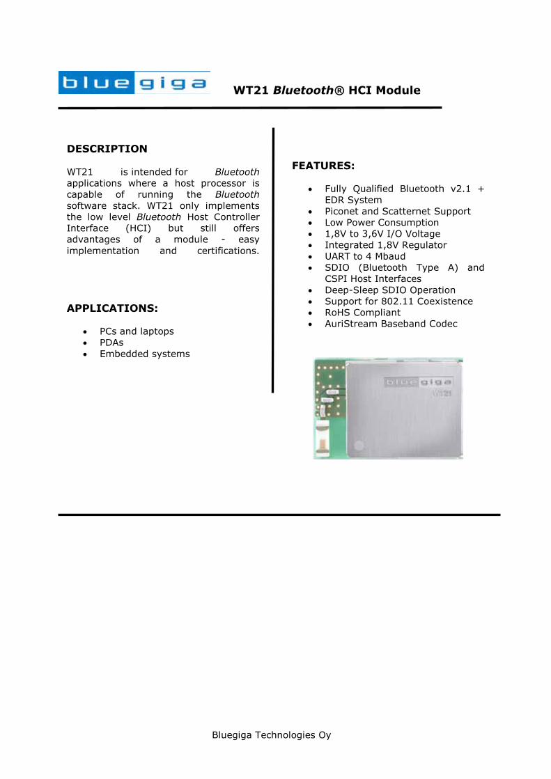
WT21 Bluetooth® HCI Module
DESCRIPTION
WT21 is intended for Bluetooth applications where a host processor is capable of running the Bluetooth software stack. WT21 only implements the low level Bluetooth Host Controller Interface (HCI) but still offers advantages of a module - easy implementation and certifications.
APPLICATIONS:
PCs and laptops PDAs Embedded systems
FEATURES:
Fully Qualified Bluetooth v2.1 + EDR System
Piconet and Scatternet Support Low Power Consumption 1,8V to 3,6V I/O Voltage Integrated 1,8V Regulator UART to 4 Mbaud SDIO (Bluetooth Type A) and
CSPI Host Interfaces Deep-Sleep SDIO Operation Support for 802.11 Coexistence RoHS Compliant AuriStream Baseband Codec

Bluegiga Technologies Oy
Page 8 of 54
1 Ordering Information
WT21-A-HCI
Product series
Fimrware HCI = HCI firmware
HW version A = Chip antenna, extended
temperature range N = RF pin, extended temperature
range
Bluegiga Technologies Oy
Page 9 of 54
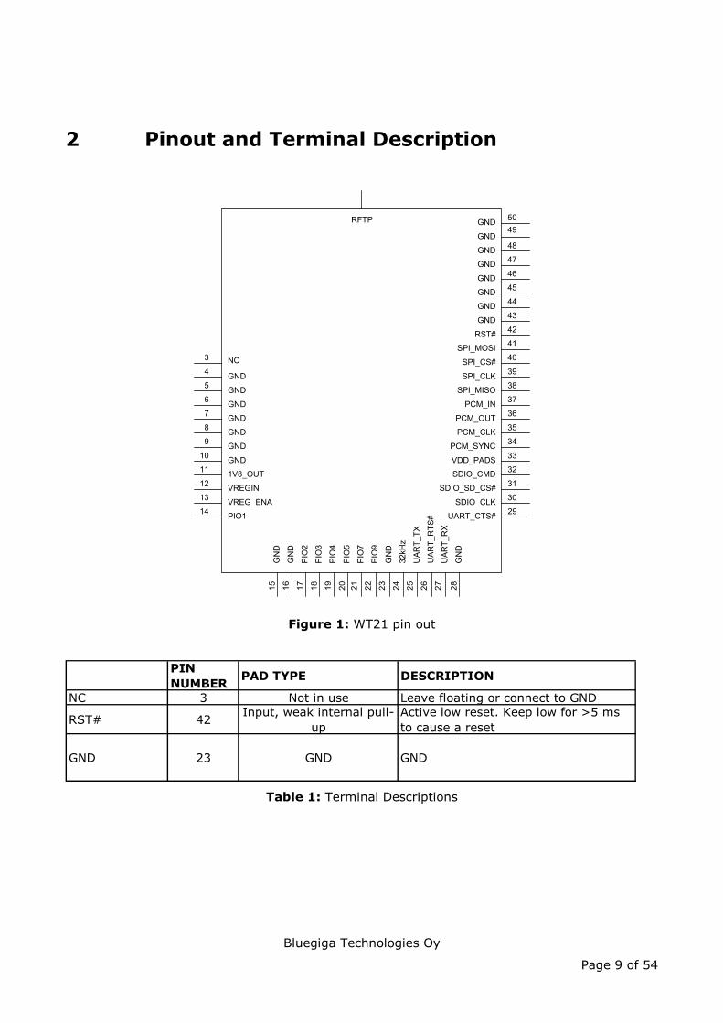
2 Pinout and Terminal Description
1V8_OUT
VREGIN
VREG_ENA
PIO1
GND
GND
GND
GND
GND
GND
GND
GN
D
PIO
2
PIO
3
PIO
4
PIO
5
PIO
7
PIO
9
GN
D
32kH
z
UAR
T_TX
UAR
T_R
TS#
UAR
T_R
X
GN
D
GN
D
UART_CTS#
SDIO_CLK
SDIO_SD_CS#
SDIO_CMD
VDD_PADS
PCM_SYNC
PCM_CLK
PCM_OUT
PCM_IN
SPI_MISO
SPI_CLK
SPI_CS#
SPI_MOSI
RST#
GND
GND
GND
GND
GND
GND
GND
GNDRFTP
4
5
6
7
8
9
10
11
12
13
14
15 16 17 18 19 20 21 22 23 24 25 26 27 28
29
30
31
32
33
34
35
36
37
38
39
40
41
42
43
44
45
46
47
48
4950
3 NC
Figure 1: WT21 pin out
PIN NUMBER PAD TYPE DESCRIPTION
NC 3 Not in use Leave floating or connect to GND
RST# 42 Input, weak internal pull-up
Active low reset. Keep low for >5 ms to cause a reset
GND 23 GND GND
Table 1: Terminal Descriptions
Bluegiga Technologies Oy
Page 10 of 54
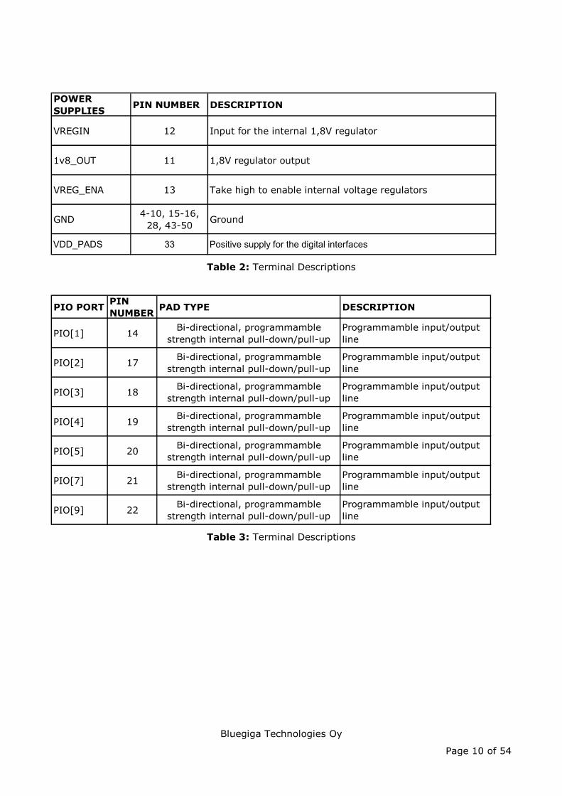
POWER SUPPLIES PIN NUMBER DESCRIPTION
VREGIN 12 Input for the internal 1,8V regulator
1v8_OUT 11 1,8V regulator output
VREG_ENA 13 Take high to enable internal voltage regulators
GND 4-10, 15-16, 28, 43-50 Ground
VDD_PADS 33 Positive supply for the digital interfaces
Table 2: Terminal Descriptions
PIO PORT PIN NUMBER PAD TYPE DESCRIPTION
PIO[1] 14 Bi-directional, programmamble strength internal pull-down/pull-up
Programmamble input/output line
PIO[2] 17 Bi-directional, programmamble strength internal pull-down/pull-up
Programmamble input/output line
PIO[3] 18 Bi-directional, programmamble strength internal pull-down/pull-up
Programmamble input/output line
PIO[4] 19 Bi-directional, programmamble strength internal pull-down/pull-up
Programmamble input/output line
PIO[5] 20 Bi-directional, programmamble strength internal pull-down/pull-up
Programmamble input/output line
PIO[7] 21 Bi-directional, programmamble strength internal pull-down/pull-up
Programmamble input/output line
PIO[9] 22 Bi-directional, programmamble strength internal pull-down/pull-up
Programmamble input/output line
Table 3: Terminal Descriptions
Bluegiga Technologies Oy
Page 11 of 54
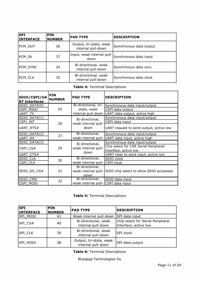
SPI INTERFACE
PIN NUMBER PAD TYPE DESCRIPTION
PCM_OUT 36 Output, tri-state, weak internal pull-down Synchronous data output
PCM_IN 37 Input, weak internal pull-down Synchronous data input
PCM_SYNC 34 Bi-directional, weak internal pull-down Synchronous data sync
PCM_CLK 35 Bi-directional, weak internal pull-down Synchronous data clock
Table 4: Terminal Descriptions
SDIO/CSPI/UART Interfaces
PIN NUMBER PAD TYPE DESCRIPTION
SDIO_DATA[0] Synchronous data input/outputCSPI_MISO CSPI data outputUART_TX UART data output, active highSDIO_DATA[1] Synchronous data input/outputCSPI_INT CSPI data input
UART_RTS# UART request to send output, active low
SDIO_DATA[2] Synchronous data input/outputUART_RX UART data input, active highSDIO_DATA[3] Synchronous data input/output
CSPI_CS# Chip select for CSR Serial Peripheral Interface, active low
UART_CTS# UART clear to send input, active lowSDIO_CLK SDIO clockCSPI_CLK CSPI clock
SDIO_SD_CS# 31Bi-directional,
weak internal pull-down
SDIO chip select to allow SDIO accessess
SDIO_CMD SDIO data inputCSPI_MOSI CSPI data input
30 Bi-directional, weak internal pull-
32 Bi-directional, weak internal pull-
27 Bi-directional, weak internal pull-
29Bi-directional,
weak internal pull-down
25Bi-directional, tri-
state, weak internal pull-down
26Bi-directional,
weak internal pull-down
Table 5: Terminal Descriptions
SPI INTERFACE
PIN NUMBER PAD TYPE DESCRIPTION
SPI_MOSI 41 Weak internal pull-down SPI data input
SPI_CS# 40 Bi-directional, weak internal pull-down
Chip select for Serial Peripheral Interface, active low
SPI_CLK 39 Bi-directional, weak internal pull-down SPI clock
SPI_MISO 38 Output, tri-state, weak internal pull-down SPI data output
Table 6: Terminal Descriptions
Bluegiga Technologies Oy
Page 12 of 54
3 Microcontroller, Memory and Baseband Logic
3.1 AuriStream CODEC
The AuriStream CODEC works on the principle of transmitting the delta between the actual value of the signal and a prediction rather than the signal itself. Hence, the information transmitted is reduced along with the power requirement. The quality of the output depends on the number of bits used to represent the sample.
The inclusion of AuriStream results in reduced power consumption compared to a CVSD implementation when used at both ends of the system.
Bluegiga Technologies Oy
Page 13 of 54
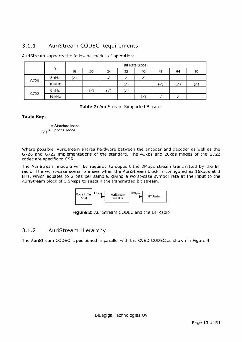
3.1.1 AuriStream CODEC Requirements
AuriStream supports the following modes of operation:
Table 7: AuriStream Supported Bitrates
Table Key:
= Standard Mode = Optional Mode
Where possible, AuriStream shares hardware between the encoder and decoder as well as the G726 and G722 implementations of the standard. The 40kbs and 20kbs modes of the G722 codec are specific to CSR.
The AuriStream module will be required to support the 3Mbps stream transmitted by the BT radio. The worst-case scenario arises when the AuriStream block is configured as 16kbps at 8 kHz, which equates to 2 bits per sample, giving a worst-case symbol rate at the input to the AuriStream block of 1.5Msps to sustain the transmitted bit stream.
Figure 2: AuriStream CODEC and the BT Radio
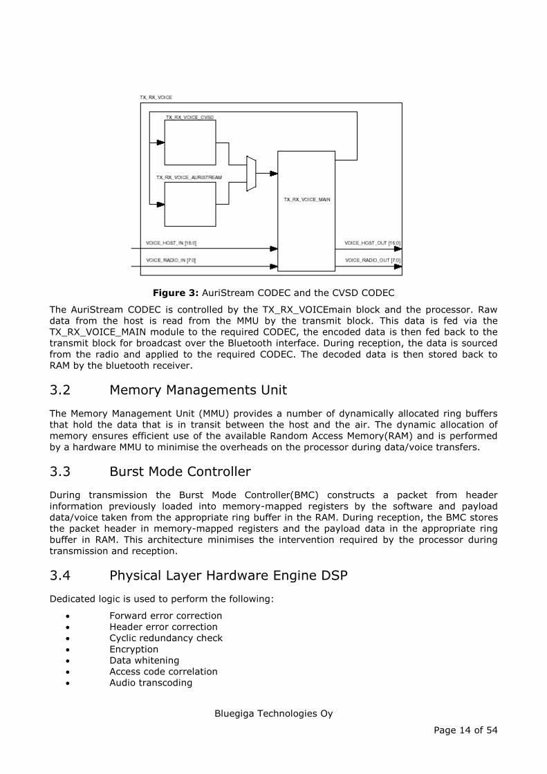
3.1.2 AuriStream Hierarchy
The AuriStream CODEC is positioned in parallel with the CVSD CODEC as shown in Figure 4.
Bluegiga Technologies Oy
Page 14 of 54
Figure 3: AuriStream CODEC and the CVSD CODEC
The AuriStream CODEC is controlled by the TX_RX_VOICEmain block and the processor. Raw data from the host is read from the MMU by the transmit block. This data is fed via the TX_RX_VOICE_MAIN module to the required CODEC, the encoded data is then fed back to the transmit block for broadcast over the Bluetooth interface. During reception, the data is sourced from the radio and applied to the required CODEC. The decoded data is then stored back to RAM by the bluetooth receiver.
3.2 Memory Managements Unit
The Memory Management Unit (MMU) provides a number of dynamically allocated ring buffers that hold the data that is in transit between the host and the air. The dynamic allocation of memory ensures efficient use of the available Random Access Memory(RAM) and is performed by a hardware MMU to minimise the overheads on the processor during data/voice transfers.
3.3 Burst Mode Controller
During transmission the Burst Mode Controller(BMC) constructs a packet from header information previously loaded into memory-mapped registers by the software and payload data/voice taken from the appropriate ring buffer in the RAM. During reception, the BMC stores the packet header in memory-mapped registers and the payload data in the appropriate ring buffer in RAM. This architecture minimises the intervention required by the processor during transmission and reception.
3.4 Physical Layer Hardware Engine DSP
Dedicated logic is used to perform the following:
Forward error correction Header error correction Cyclic redundancy check Encryption Data whitening Access code correlation Audio transcoding
Bluegiga Technologies Oy
Page 15 of 54
The following voice data translations and operations are performed by firmware:
A-law/µ-law/linear voice data (from host) A-law/µ-law/Continuously variable Slope Delta (CVSD) (over the air) Voice interpolation for lost packets Rate mismatches
The hardware supports all optional and mandatory features of Bluetooth v2.1 + EDR including AFH and eSCO.
3.5 WLAN Coexistence
Dedicated hardware is provided to implement a variety of coexistence schemes. Channel skipping AFH, priority signalling, channel signalling and host passing of channel instructions are all supported. The features are configured in firmware.
For more information contact Buegiga technical support.
3.6 Configurable I/O Parallel Ports
lines of programmable bi-directional input/outputs (I/O) are provided. PIO[1: 5, 7, 9] are powered from VDD_PADS.
PIO lines can be configured through software to have either weak or strong pull-ups or pull-downs. All PIO lines are configured as inputs with weak pull-downs at reset.
Any of the PIO lines can be configured as interrupt request lines or as wake-up lines from sleep modes.
Bluegiga cannot guarantee that the PIO assignments remain as described. Refer to the relevant software release note for the implementation of these PIO lines, as they are firmware build-specific.
Bluegiga Technologies Oy
Page 16 of 54
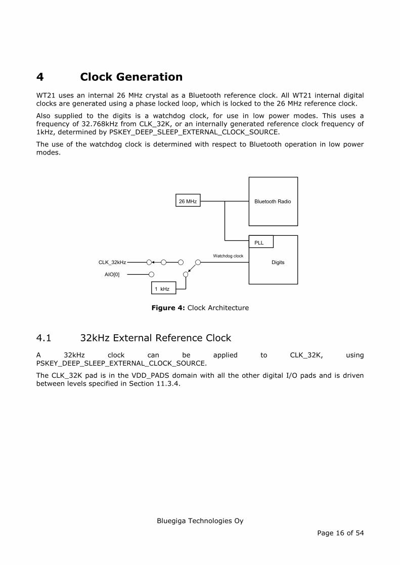
4 Clock Generation WT21 uses an internal 26 MHz crystal as a Bluetooth reference clock. All WT21 internal digital clocks are generated using a phase locked loop, which is locked to the 26 MHz reference clock.
Also supplied to the digits is a watchdog clock, for use in low power modes. This uses a frequency of 32.768kHz from CLK_32K, or an internally generated reference clock frequency of 1kHz, determined by PSKEY_DEEP_SLEEP_EXTERNAL_CLOCK_SOURCE.
The use of the watchdog clock is determined with respect to Bluetooth operation in low power modes.
Bluetooth Radio
Digits
PLL
26 MHz
1 kHz
CLK_32kHz
AIO[0]
Watchdog clock
Figure 4: Clock Architecture
4.1 32kHz External Reference Clock
A 32kHz clock can be applied to CLK_32K, using PSKEY_DEEP_SLEEP_EXTERNAL_CLOCK_SOURCE.
The CLK_32K pad is in the VDD_PADS domain with all the other digital I/O pads and is driven between levels specified in Section 11.3.4.
Bluegiga Technologies Oy
Page 17 of 54
5 Serial Peripheral Interface (SPI)
5.1 WT21 Serial Peripheral Interface (SPI)
SPI is used for debuging primarily. This section details the considerations required when interfacing to WT21 via the SPI.
Data may be written or read one word at a time or the auto increment feature may be used to access blocks.
5.2 Instruction Cycle
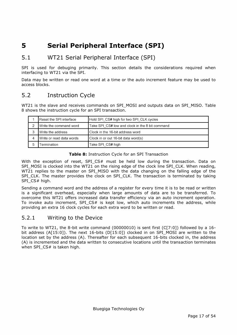
WT21 is the slave and receives commands on SPI_MOSI and outputs data on SPI_MISO. Table 8 shows the instruction cycle for an SPI transaction.
Table 8: Instruction Cycle for an SPI Transaction
With the exception of reset, SPI_CS# must be held low during the transaction. Data on SPI_MOSI is clocked into the WT21 on the rising edge of the clock line SPI_CLK. When reading, WT21 replies to the master on SPI_MISO with the data changing on the falling edge of the SPI_CLK. The master provides the clock on SPI_CLK. The transaction is terminated by taking SPI_CS# high.
Sending a command word and the address of a register for every time it is to be read or written is a significant overhead, especially when large amounts of data are to be transferred. To overcome this WT21 offers increased data transfer efficiency via an auto increment operation. To invoke auto increment, SPI_CS# is kept low, which auto increments the address, while providing an extra 16 clock cycles for each extra word to be written or read.
5.2.1 Writing to the Device
To write to WT21, the 8-bit write command (00000010) is sent first (C[7:0]) followed by a 16-bit address (A[15:0]). The next 16-bits (D[15:0]) clocked in on SPI_MOSI are written to the location set by the address (A). Thereafter for each subsequent 16-bits clocked in, the address (A) is incremented and the data written to consecutive locations until the transaction terminates when SPI_CS# is taken high.
Bluegiga Technologies Oy
Page 18 of 54
Figure 5: SPI Write Operation
5.2.2 Reading from the Device
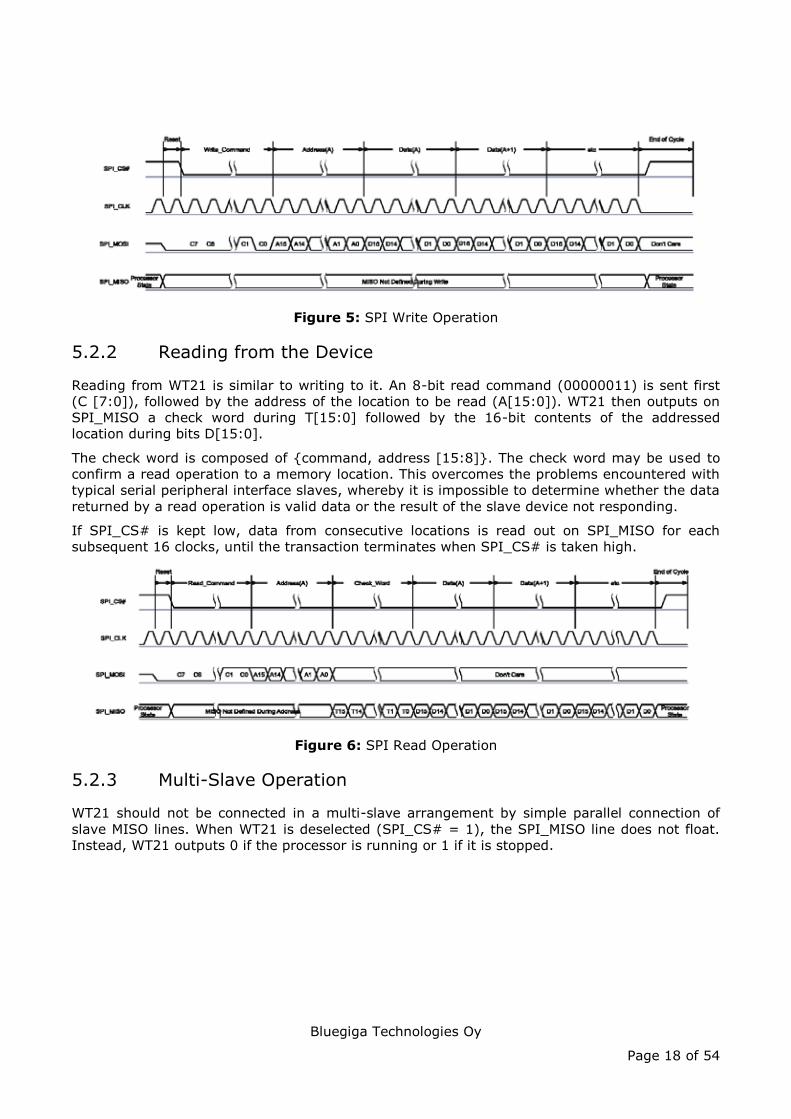
Reading from WT21 is similar to writing to it. An 8-bit read command (00000011) is sent first (C [7:0]), followed by the address of the location to be read (A[15:0]). WT21 then outputs on SPI_MISO a check word during T[15:0] followed by the 16-bit contents of the addressed location during bits D[15:0].
The check word is composed of {command, address [15:8]}. The check word may be used to confirm a read operation to a memory location. This overcomes the problems encountered with typical serial peripheral interface slaves, whereby it is impossible to determine whether the data returned by a read operation is valid data or the result of the slave device not responding.
If SPI_CS# is kept low, data from consecutive locations is read out on SPI_MISO for each subsequent 16 clocks, until the transaction terminates when SPI_CS# is taken high.
Figure 6: SPI Read Operation
5.2.3 Multi-Slave Operation
WT21 should not be connected in a multi-slave arrangement by simple parallel connection of slave MISO lines. When WT21 is deselected (SPI_CS# = 1), the SPI_MISO line does not float. Instead, WT21 outputs 0 if the processor is running or 1 if it is stopped.
Bluegiga Technologies Oy
Page 19 of 54
6 Host Interfaces
6.1 Host Selection
The MCU selects the UART/SDIO interfaces by reading PIO[4] at boot-time. When PIO[4] is high, the SDIO interface is enabled; when PIO[4] is low, the UART is enabled.
If in UART mode, the MCU selects the UART transfer protocol automatically using the unused SDIO pins shown in Table 9
SDIO_CLK SDIO_CMD Protocol0 0 bcsp0 1 h41 0 h4ds1 1 h5
Table 9: SDIO_CLK and SDIO_CMD transfer Protocols
6.2 UART Interface
This is a standard UART interface for communicating with other serial devices.
WT21 UART interface provides a simple mechanism for communicating with other serial devices using the RS232 protocol.
Note:
WT21 uses RS232 protocol, but voltage levels are 0V to VDD_PADS (requires external RS232 transceiver chip.
UART_TX
UART_RX
UART_RTS#
UART_CTS#
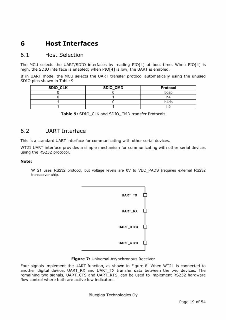
Figure 7: Universal Asynchronous Receiver
Four signals implement the UART function, as shown in Figure 8. When WT21 is connected to another digital device, UART_RX and UART_TX transfer data between the two devices. The remaining two signals, UART_CTS and UART_RTS, can be used to implement RS232 hardware flow control where both are active low indicators.
Bluegiga Technologies Oy
Page 20 of 54
UART configuration parameters, such as baud rate and packet format, are set using WT21 firmware.
Note:
An accelerated serial port adapter is required to communicate with the UART at maximum baud rate using a standard PC.
Table 10: Possible UART Settings
Note:
Baud rate is the measure of symbol rate i.e. , the number of distinct symbol changes (signaling events) made to transmission medium per second in a digitally modulated signal.
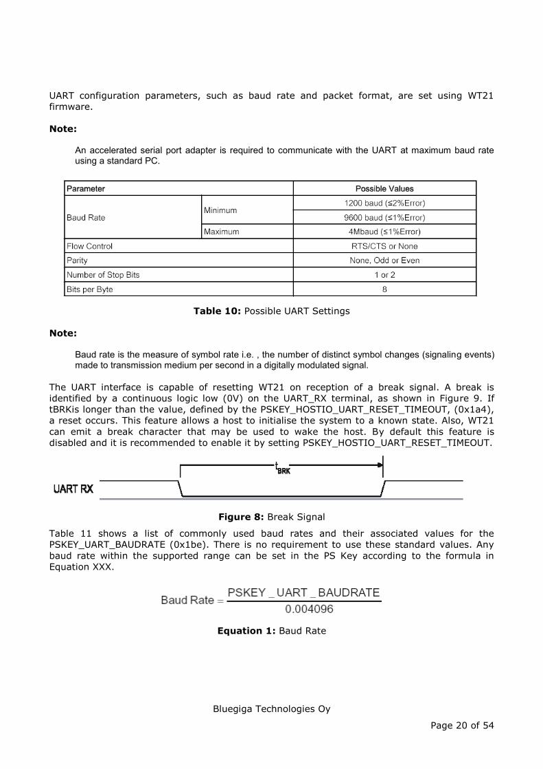
The UART interface is capable of resetting WT21 on reception of a break signal. A break is identified by a continuous logic low (0V) on the UART_RX terminal, as shown in Figure 9. If tBRKis longer than the value, defined by the PSKEY_HOSTIO_UART_RESET_TIMEOUT, (0x1a4), a reset occurs. This feature allows a host to initialise the system to a known state. Also, WT21 can emit a break character that may be used to wake the host. By default this feature is disabled and it is recommended to enable it by setting PSKEY_HOSTIO_UART_RESET_TIMEOUT.
Figure 8: Break Signal
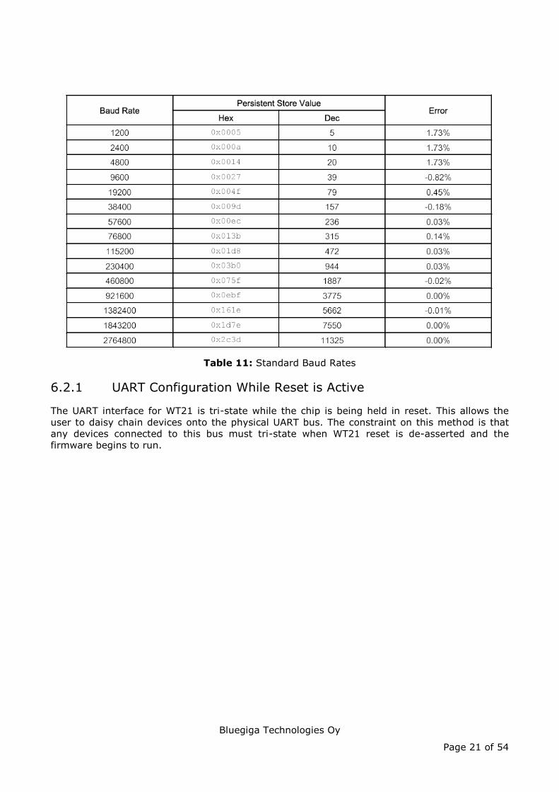
Table 11 shows a list of commonly used baud rates and their associated values for the PSKEY_UART_BAUDRATE (0x1be). There is no requirement to use these standard values. Any baud rate within the supported range can be set in the PS Key according to the formula in Equation XXX.
Equation 1: Baud Rate
Bluegiga Technologies Oy
Page 21 of 54
Table 11: Standard Baud Rates
6.2.1 UART Configuration While Reset is Active
The UART interface for WT21 is tri-state while the chip is being held in reset. This allows the user to daisy chain devices onto the physical UART bus. The constraint on this method is that any devices connected to this bus must tri-state when WT21 reset is de-asserted and the firmware begins to run.

Bluegiga Technologies Oy
Page 22 of 54
7 CSR Serial Peripheral Interface (CSPI) The CSPI is a host interface which shares pins with the SDIO. It has been defined by CSR with the intention of producing a very simple interface. This has two advantages:
It allows maximum compatibility with the possible host drivers It minimizes the host software effort needed to form that data to be sent (e.g., by removing the need to calculate CRCs)
This host interface allows an external host to control the Bluecore, using a CSR defined protocol built upon a 4-wire SPI bus.
Note:
The CSPI is entirely separated from the debug Serial Peripheral Interface
The CSPI allows access to the following:
Function 0 registers Bluetooth Acceleration Registers MCU IO Registers Bluetooth MMU port
The CSPI is a third protocol available for the host to transfer data into the Bluecore and shares pins with the other SDIO protocols.
MMU buffers are accessed using burst read/writes. The command and address fields are used to select the correct buffer. The CSPI is able to generate an interrupt to the host when a memory access fails. This interrupt line is shared with the SDIO functions.
Table 12 shows the mapping of SDIO pins onto the CSPI functions when CSPI is enabled.
Table 12: SDIO Mapping to CSPI Functions
The CSPI Interface is an extension of the basic SPI Interface, with the access type determined by the following fields:
8-bit command 24-bit address 16-bit burst length (optional). Only applicable for burst transfers into or out of the MMU
7.1.1 CSPI Read/Write Cycles
Register read/write cycles are used to access Function 0, Bluetooth acceleration and MCU registers.
Burst read/write cycles are used to access the MMU.
Bluegiga Technologies Oy
Page 23 of 54
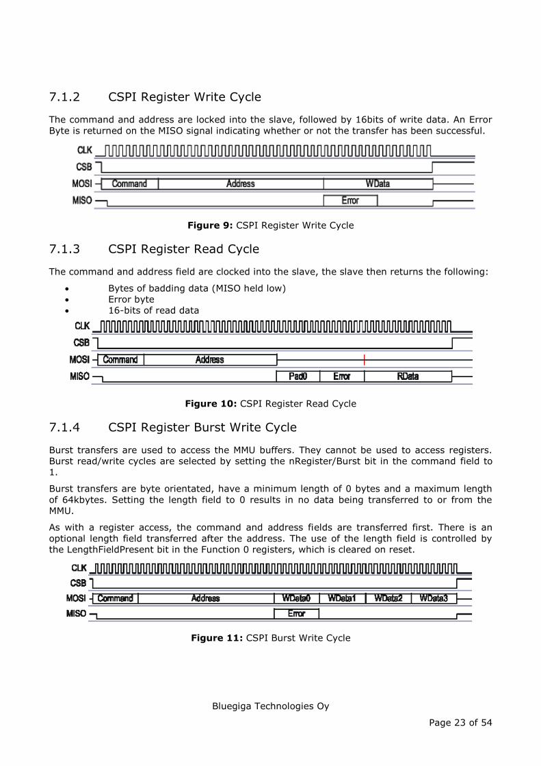
7.1.2 CSPI Register Write Cycle
The command and address are locked into the slave, followed by 16bits of write data. An Error Byte is returned on the MISO signal indicating whether or not the transfer has been successful.
Figure 9: CSPI Register Write Cycle
7.1.3 CSPI Register Read Cycle
The command and address field are clocked into the slave, the slave then returns the following:
Bytes of badding data (MISO held low) Error byte 16-bits of read data
Figure 10: CSPI Register Read Cycle
7.1.4 CSPI Register Burst Write Cycle
Burst transfers are used to access the MMU buffers. They cannot be used to access registers. Burst read/write cycles are selected by setting the nRegister/Burst bit in the command field to 1.
Burst transfers are byte orientated, have a minimum length of 0 bytes and a maximum length of 64kbytes. Setting the length field to 0 results in no data being transferred to or from the MMU.
As with a register access, the command and address fields are transferred first. There is an optional length field transferred after the address. The use of the length field is controlled by the LengthFieldPresent bit in the Function 0 registers, which is cleared on reset.
Figure 11: CSPI Burst Write Cycle
Bluegiga Technologies Oy
Page 24 of 54
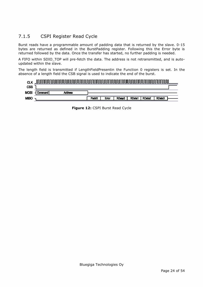
7.1.5 CSPI Register Read Cycle
Burst reads have a programmable amount of padding data that is returned by the slave. 0-15 bytes are returned as defined in the BurstPadding register. Following this the Error byte is returned followed by the data. Once the transfer has started, no further padding is needed.
A FIFO within SDIO_TOP will pre-fetch the data. The address is not retransmitted, and is auto-updated within the slave.
The length field is transmitted if LengthFieldPresentin the Function 0 registers is set. In the absence of a length field the CSB signal is used to indicate the end of the burst.
Figure 12: CSPI Burst Read Cycle
Bluegiga Technologies Oy
Page 25 of 54
7.2 SDIO Interface
This is a host interface which allows a Secure Digital Input Output(SDIO) host to gain access to the internals of the chip. It provides all defined slave modes (SPI, SD 1bit, SD 4bit), but not SD host function.
The function provided includes generating responses to each command in hardware and implementing the state machines defined in the SDIO specification. Within the various modes of operation, it provides initialisation functions (cmds 0, 3, 5, 7, 15, 59) and two other functions:
Function 1 provides Bluetooth type A support, and follows that specification Function 2 provides generic register access(cmd52 (byte read/write))
For more information, see the following specifications:
SD Specifications Part 1 Physical Layer Specification v.1.10 SD Specification Part E1 SDIO Specification v.1.10 SDIO Card Part E2 Type-A Specification for Bluetooth v.1.00
7.2.1 SDIO/CSPI Deep-Sleep Control Schemes
This is the lowest power mode, where the processor, the internal reference (fast) clock, and much of the digital and analogue hardware are shut down. To support this power consumption reduction solution and to prevent any errors arising on the SDIO host interface there are two Deep-Sleep control schemes.
Scheme 1: The host retransmits any packets that Bluecore was unable to receive as a result of being in Deep-Sleep Scheme 2: Introduces additional signaling to prevent the need for retransmissions
During Deep-Sleep the internal reference clock is turned off. However, the host transport protocols (SD/UART/CSPI) are driven from the SDIO clock and so continue to function during Deep-Sleep, enabling access to the function 0 interface, but not the function 1 interface.
7.2.2 Retransmission
Bluecore enters Deep-Sleep whenever it becomes idle after which time, when the host transmits a message on function 1 an illegal command error will be signaled. The activity that this initiates on the SDIO Interface provokes Bluecore into wakeup after which the host re-transmits the original message.
Bluecore will wait for a configurable period of time before re-entering Deep-Sleep, thus ensuring that the original packet is sent/received on retransmission. This control scheme is the default mode of operation.
7.2.3 Signaling
Signalling between the host and Bluecore enables host control over Bluecore Deep-Sleep mode. Consequently the host is aware of when it is appropriate to send Bluecore HCI traffic over function 1.
The signals used by this scheme are Host wakeup and Ready status interrupt select, implemented as register bit in the vendor unique area of function 0.
Bluegiga Technologies Oy
Page 26 of 54
8 Audio Interfaces
8.1 PCM Interface
The audio Pulse Code Modulation(PCM) interface supports continuous transmission and reception of PCM encoded audio data over Bluetooth.
Pulse Code Modulation (PCM) is a standard method used to digitise audio (particularly voice) for transmission over digital communication channels. Through its PCM interface, WT21 has hardware support for continual transmission and reception of PCM data, thus reducing processor overhead for wireless headset applications. BlueCore6-ROM (QFN) offers a bi-directional digital audio interface that routes directly into the baseband layer of the on-chip firmware. It does not pass through the HCI protocol layer.
Hardware on WT21 allows the data to be sent to and received from a SCO connection.
Up to three SCO connections can be supported by the PCM interface at any one time.
WT21 can operate as the PCM interface master generating an output clock of 128, 256, 512, 1536 or 2400kHz. When configured as a PCM interface slave, it can operate with an input clock up to 2400kHz. WT21 is compatible with a variety of clock formats, including Long Frame Sync, Short Frame Sync and GCI timing environments.
It supports 13-bit or 16-bit linear, 8-bit μ-law or A-law companded sample formats at 8ksamples/s and can receive and transmit on any selection of three of the first four slots following PCM_SYNC. The PCM configuration options are enabled by setting the PSKEY_PCM_CONFIG32 (0x1b3).
WT21 interfaces directly to PCM audio devices including the following:
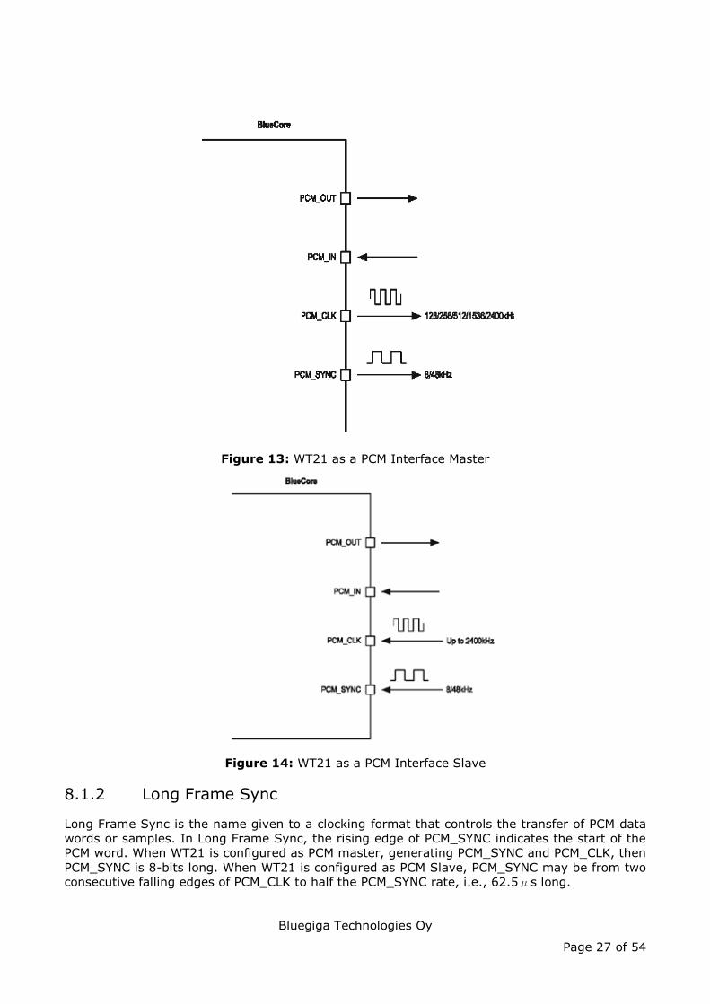
8.1.1 PCM Interface Master/Slave
When configured as the master of the PCM interface, BlueCore6-ROM (QFN) generates PCM_CLK and PCM_SYNC.
Bluegiga Technologies Oy
Page 27 of 54
Figure 13: WT21 as a PCM Interface Master
Figure 14: WT21 as a PCM Interface Slave
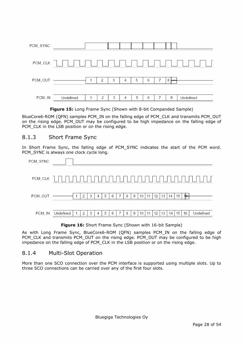
8.1.2 Long Frame Sync
Long Frame Sync is the name given to a clocking format that controls the transfer of PCM data words or samples. In Long Frame Sync, the rising edge of PCM_SYNC indicates the start of the PCM word. When WT21 is configured as PCM master, generating PCM_SYNC and PCM_CLK, then PCM_SYNC is 8-bits long. When WT21 is configured as PCM Slave, PCM_SYNC may be from two consecutive falling edges of PCM_CLK to half the PCM_SYNC rate, i.e., 62.5μs long.
Bluegiga Technologies Oy
Page 28 of 54
Figure 15: Long Frame Sync (Shown with 8-bit Companded Sample)
BlueCore6-ROM (QFN) samples PCM_IN on the falling edge of PCM_CLK and transmits PCM_OUT on the rising edge. PCM_OUT may be configured to be high impedance on the falling edge of PCM_CLK in the LSB position or on the rising edge.
8.1.3 Short Frame Sync
In Short Frame Sync, the falling edge of PCM_SYNC indicates the start of the PCM word. PCM_SYNC is always one clock cycle long.
Figure 16: Short Frame Sync (Shown with 16-bit Sample)
As with Long Frame Sync, BlueCore6-ROM (QFN) samples PCM_IN on the falling edge of PCM_CLK and transmits PCM_OUT on the rising edge. PCM_OUT may be configured to be high impedance on the falling edge of PCM_CLK in the LSB position or on the rising edge.
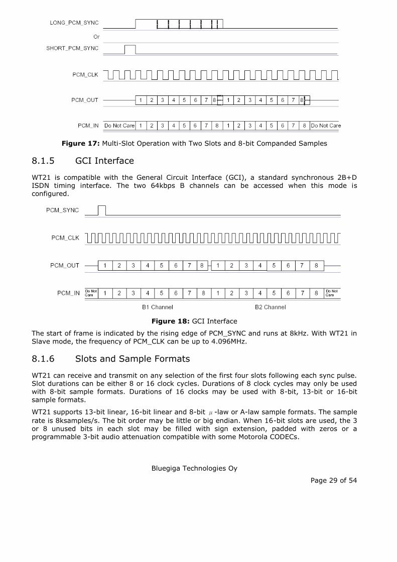
8.1.4 Multi-Slot Operation
More than one SCO connection over the PCM interface is supported using multiple slots. Up to three SCO connections can be carried over any of the first four slots.
Bluegiga Technologies Oy
Page 29 of 54
Figure 17: Multi-Slot Operation with Two Slots and 8-bit Companded Samples
8.1.5 GCI Interface
WT21 is compatible with the General Circuit Interface (GCI), a standard synchronous 2B+D ISDN timing interface. The two 64kbps B channels can be accessed when this mode is configured.
Figure 18: GCI Interface
The start of frame is indicated by the rising edge of PCM_SYNC and runs at 8kHz. With WT21 in Slave mode, the frequency of PCM_CLK can be up to 4.096MHz.
8.1.6 Slots and Sample Formats
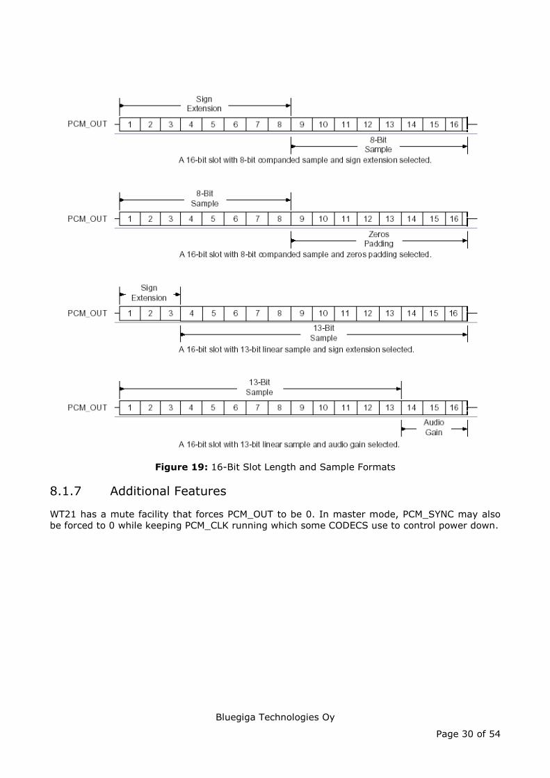
WT21 can receive and transmit on any selection of the first four slots following each sync pulse. Slot durations can be either 8 or 16 clock cycles. Durations of 8 clock cycles may only be used with 8-bit sample formats. Durations of 16 clocks may be used with 8-bit, 13-bit or 16-bit sample formats.
WT21 supports 13-bit linear, 16-bit linear and 8-bit μ-law or A-law sample formats. The sample rate is 8ksamples/s. The bit order may be little or big endian. When 16-bit slots are used, the 3 or 8 unused bits in each slot may be filled with sign extension, padded with zeros or a programmable 3-bit audio attenuation compatible with some Motorola CODECs.
Bluegiga Technologies Oy
Page 30 of 54
Figure 19: 16-Bit Slot Length and Sample Formats
8.1.7 Additional Features
WT21 has a mute facility that forces PCM_OUT to be 0. In master mode, PCM_SYNC may also be forced to 0 while keeping PCM_CLK running which some CODECS use to control power down.
Bluegiga Technologies Oy
Page 31 of 54
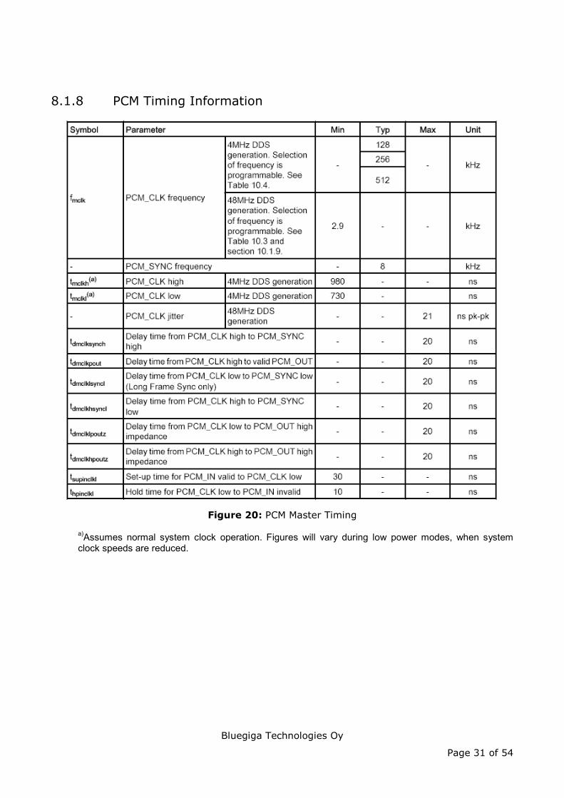
8.1.8 PCM Timing Information
Figure 20: PCM Master Timing
a)Assumes normal system clock operation. Figures will vary during low power modes, when system clock speeds are reduced.
Bluegiga Technologies Oy
Page 32 of 54
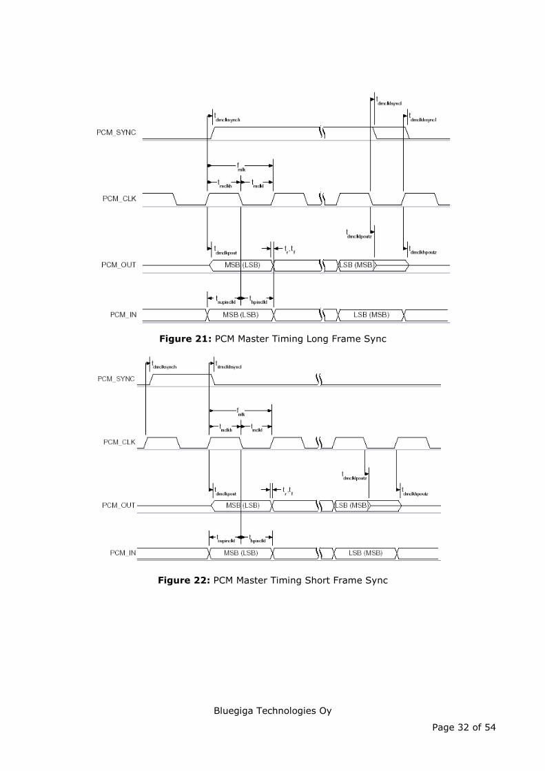
Figure 21: PCM Master Timing Long Frame Sync
Figure 22: PCM Master Timing Short Frame Sync
Bluegiga Technologies Oy
Page 33 of 54
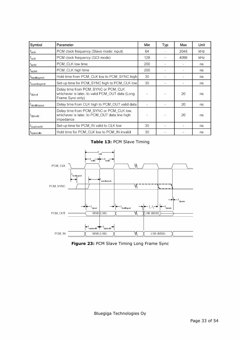
Table 13: PCM Slave Timing
Figure 23: PCM Slave Timing Long Frame Sync
Bluegiga Technologies Oy
Page 34 of 54
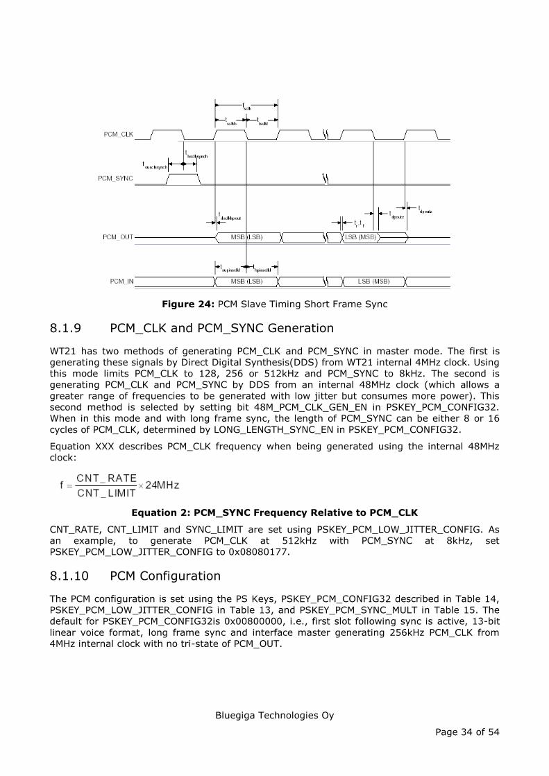
Figure 24: PCM Slave Timing Short Frame Sync
8.1.9 PCM_CLK and PCM_SYNC Generation
WT21 has two methods of generating PCM_CLK and PCM_SYNC in master mode. The first is generating these signals by Direct Digital Synthesis(DDS) from WT21 internal 4MHz clock. Using this mode limits PCM_CLK to 128, 256 or 512kHz and PCM_SYNC to 8kHz. The second is generating PCM_CLK and PCM_SYNC by DDS from an internal 48MHz clock (which allows a greater range of frequencies to be generated with low jitter but consumes more power). This second method is selected by setting bit 48M_PCM_CLK_GEN_EN in PSKEY_PCM_CONFIG32. When in this mode and with long frame sync, the length of PCM_SYNC can be either 8 or 16 cycles of PCM_CLK, determined by LONG_LENGTH_SYNC_EN in PSKEY_PCM_CONFIG32.
Equation XXX describes PCM_CLK frequency when being generated using the internal 48MHz clock:
Equation 2: PCM_SYNC Frequency Relative to PCM_CLK
CNT_RATE, CNT_LIMIT and SYNC_LIMIT are set using PSKEY_PCM_LOW_JITTER_CONFIG. As an example, to generate PCM_CLK at 512kHz with PCM_SYNC at 8kHz, set PSKEY_PCM_LOW_JITTER_CONFIG to 0x08080177.
8.1.10 PCM Configuration
The PCM configuration is set using the PS Keys, PSKEY_PCM_CONFIG32 described in Table 14, PSKEY_PCM_LOW_JITTER_CONFIG in Table 13, and PSKEY_PCM_SYNC_MULT in Table 15. The default for PSKEY_PCM_CONFIG32is 0x00800000, i.e., first slot following sync is active, 13-bit linear voice format, long frame sync and interface master generating 256kHz PCM_CLK from 4MHz internal clock with no tri-state of PCM_OUT.
Bluegiga Technologies Oy
Page 35 of 54
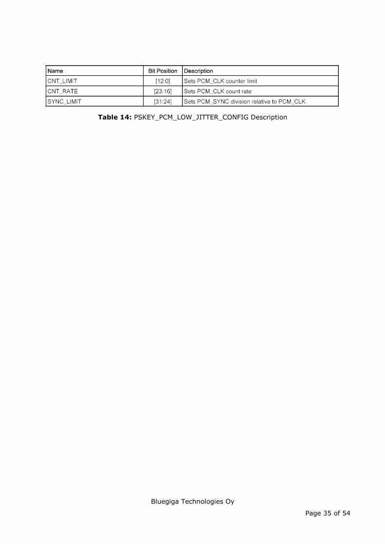
Table 14: PSKEY_PCM_LOW_JITTER_CONFIG Description
Bluegiga Technologies Oy
Page 36 of 54
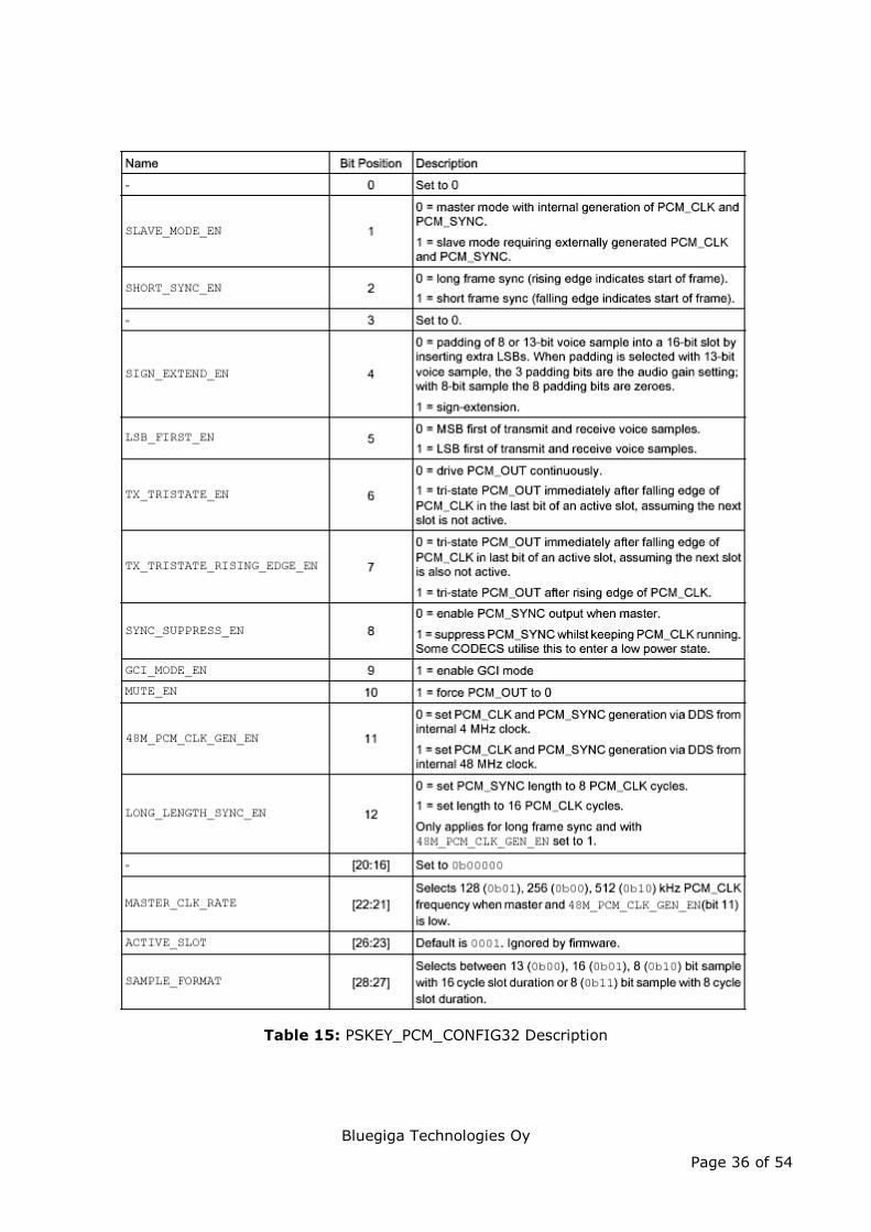
Table 15: PSKEY_PCM_CONFIG32 Description
Bluegiga Technologies Oy
Page 37 of 54
Table 16: PSKEY_PCM_SYNC_MULT Description
8.2 Digital Audio Interface (I2S)
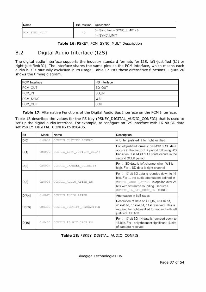
The digital audio interface supports the industry standard formats for I2S, left-justified (LJ) or right-justified(RJ). The interface shares the same pins as the PCM interface, which means each audio bus is mutually exclusive in its usage. Table 17 lists these alternative functions. Figure 26 shows the timing diagram.
Table 17: Alternative Functions of the Digital Audio Bus Interface on the PCM Interface.
Table 18 describes the values for the PS Key (PSKEY_DIGITAL_AUDIO_CONFIG) that is used to set-up the digital audio interface. For example, to configure an I2S interface with 16-bit SD data set PSKEY_DIGITAL_CONFIG to 0x0406.
Table 18: PSKEY_DIGITAL_AUDIO_CONFIG
Bluegiga Technologies Oy
Page 38 of 54
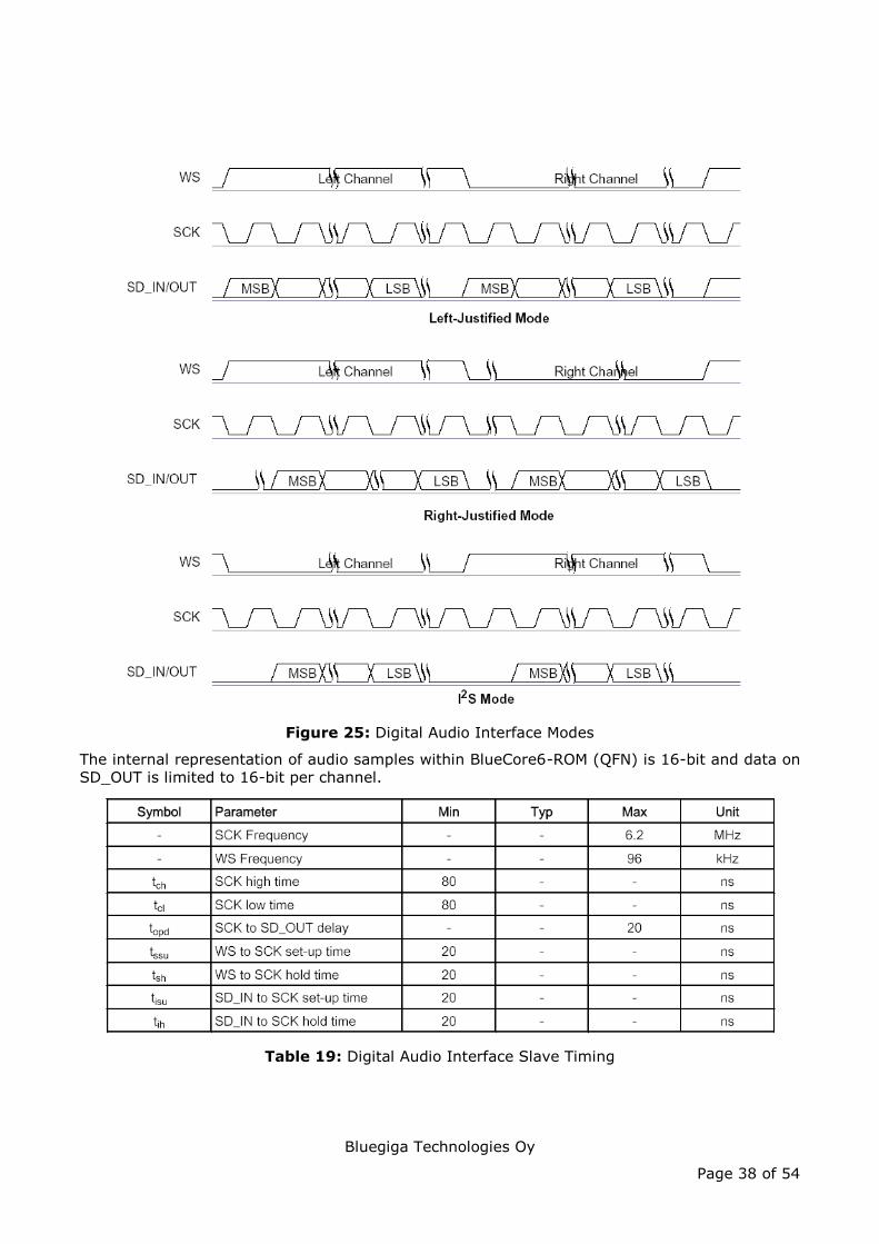
Figure 25: Digital Audio Interface Modes
The internal representation of audio samples within BlueCore6-ROM (QFN) is 16-bit and data on SD_OUT is limited to 16-bit per channel.
Table 19: Digital Audio Interface Slave Timing
Bluegiga Technologies Oy
Page 39 of 54
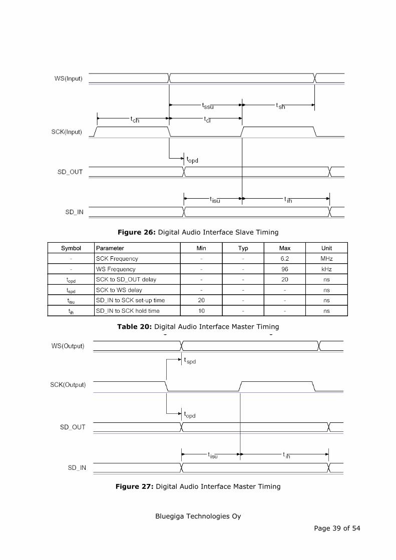
Figure 26: Digital Audio Interface Slave Timing
Table 20: Digital Audio Interface Master Timing
Figure 27: Digital Audio Interface Master Timing
Bluegiga Technologies Oy
Page 40 of 54
9 Power Control and Regulation
9.1 Power Control and Regulation
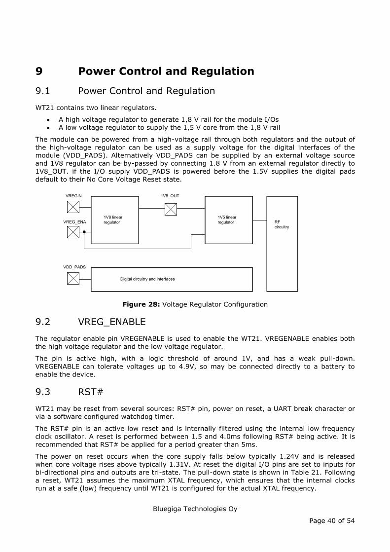
WT21 contains two linear regulators.
A high voltage regulator to generate 1,8 V rail for the module I/Os A low voltage regulator to supply the 1,5 V core from the 1,8 V rail
The module can be powered from a high-voltage rail through both regulators and the output of the high-voltage regulator can be used as a supply voltage for the digital interfaces of the module (VDD_PADS). Alternatively VDD_PADS can be supplied by an external voltage source and 1V8 regulator can be by-passed by connecting 1.8 V from an external regulator directly to 1V8_OUT. if the I/O supply VDD_PADS is powered before the 1.5V supplies the digital pads default to their No Core Voltage Reset state.
1V8_OUTVREGIN
VREG_ENA1V8 linear regulator
1V5 linear regulator RF
circuitry
VDD_PADS
Digital circuitry and interfaces
Figure 28: Voltage Regulator Configuration
9.2 VREG_ENABLE
The regulator enable pin VREGENABLE is used to enable the WT21. VREGENABLE enables both the high voltage regulator and the low voltage regulator.
The pin is active high, with a logic threshold of around 1V, and has a weak pull-down. VREGENABLE can tolerate voltages up to 4.9V, so may be connected directly to a battery to enable the device.
9.3 RST#
WT21 may be reset from several sources: RST# pin, power on reset, a UART break character or via a software configured watchdog timer.
The RST# pin is an active low reset and is internally filtered using the internal low frequency clock oscillator. A reset is performed between 1.5 and 4.0ms following RST# being active. It is recommended that RST# be applied for a period greater than 5ms.
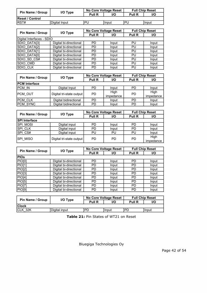
The power on reset occurs when the core supply falls below typically 1.24V and is released when core voltage rises above typically 1.31V. At reset the digital I/O pins are set to inputs for bi-directional pins and outputs are tri-state. The pull-down state is shown in Table 21. Following a reset, WT21 assumes the maximum XTAL frequency, which ensures that the internal clocks run at a safe (low) frequency until WT21 is configured for the actual XTAL frequency.
Bluegiga Technologies Oy
Page 41 of 54
9.4 Digital Pin States on Reset
The digital I/O interfaces on the WT21 device are optimised for minimum power consumption after initialisation of digital interfaces.
Table 21 shows the pin states of WT21 on reset. Pull-up (PU) and pull-down (PD) default to weak values unless specified otherwise.
Bluegiga Technologies Oy
Page 42 of 54
Pull R I/O Pull R I/O
RST# Digital Input PU Input PU Input
Pull R I/O Pull R I/O
SDIO_DATA[3] Digital bi-directional PD Input PU InputSDIO_DATA[2] Digital bi-directional PD Input PU InputSDIO_DATA[1] Digital bi-directional PD Input PU InputSDIO_DATA[0] Digital bi-directional PD Input PU InputSDIO_SD_CS# Digital bi-directional PD Input PU InputSDIO_CMD Digital bi-directional PD Input PU InputSDIO_CLK Digital bi-directional PD Input PU Input
Pull R I/O Pull R I/O
PCM_IN Digital Input PD Input PD Input
PCM_OUT Digital tri-state output PD High impedance PD High
impedancePCM_CLK Digital bidirectional PD Input PD InputPCM_SYNC Digital bidirectional PD Input PD Input
Pull R I/O Pull R I/O
SPI_MOSI Digital input PD Input PD InputSPI_CLK Digital input PD Input PD InputSPI_CS# Digital input PU PU PU Input
SPI_MISO Digital tri-state output PD PD PD High impedance
Pull R I/O Pull R I/O
PIO[0] Digital bi-directional PD Input PD InputPIO[1] Digital bi-directional PD Input PD InputPIO[2] Digital bi-directional PD Input PD InputPIO[3] Digital bi-directional PD Input PD InputPIO[4] Digital bi-directional PD Input PD InputPIO[5] Digital bi-directional PD Input PD InputPIO[7] Digital bi-directional PD Input PD InputPIO[9] Digital bi-directional PD Input PD Input
Pull R I/O Pull R I/O
CLK_32K Digital input PD Input PD Input
PIOs
SPI Interface
Pin Name / Group I/O Type No Core Voltage Reset Full Chip Reset
Pin Name / Group I/O Type No Core Voltage Reset Full Chip Reset
Pin Name / Group I/O Type No Core Voltage Reset Full Chip Reset
Reset / Control
Pin Name / Group I/O Type Full Chip Reset
PCM Interface
Digital Interfaces - SDIO
No Core Voltage Reset
Pin Name / Group I/O Type No Core Voltage Reset Full Chip Reset
Clock
Pin Name / Group I/O Type No Core Voltage Reset Full Chip Reset
Table 21: Pin States of WT21 on Reset
Bluegiga Technologies Oy
Page 43 of 54
10 Bluetooth Radio
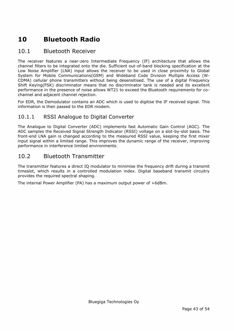
10.1 Bluetooth Receiver
The receiver features a near-zero Intermediate Frequency (IF) architecture that allows the channel filters to be integrated onto the die. Sufficient out-of-band blocking specification at the Low Noise Amplifier (LNA) input allows the receiver to be used in close proximity to Global System for Mobile Communications(GSM) and Wideband Code Division Multiple Access (W-CDMA) cellular phone transmitters without being desensitised. The use of a digital Frequency Shift Keying(FSK) discriminator means that no discriminator tank is needed and its excellent performance in the presence of noise allows WT21 to exceed the Bluetooth requirements for co-channel and adjacent channel rejection.
For EDR, the Demodulator contains an ADC which is used to digitise the IF received signal. This information is then passed to the EDR modem.
10.1.1 RSSI Analogue to Digital Converter
The Analogue to Digital Converter (ADC) implements fast Automatic Gain Control (AGC). The ADC samples the Received Signal Strength Indicator (RSSI) voltage on a slot-by-slot basis. The front-end LNA gain is changed according to the measured RSSI value, keeping the first mixer input signal within a limited range. This improves the dynamic range of the receiver, improving performance in interference limited environments.
10.2 Bluetooth Transmitter
The transmitter features a direct IQ modulator to minimise the frequency drift during a transmit timeslot, which results in a controlled modulation index. Digital baseband transmit circuitry provides the required spectral shaping.
The internal Power Amplifier (PA) has a maximum output power of +6dBm.
Bluegiga Technologies Oy
Page 44 of 54
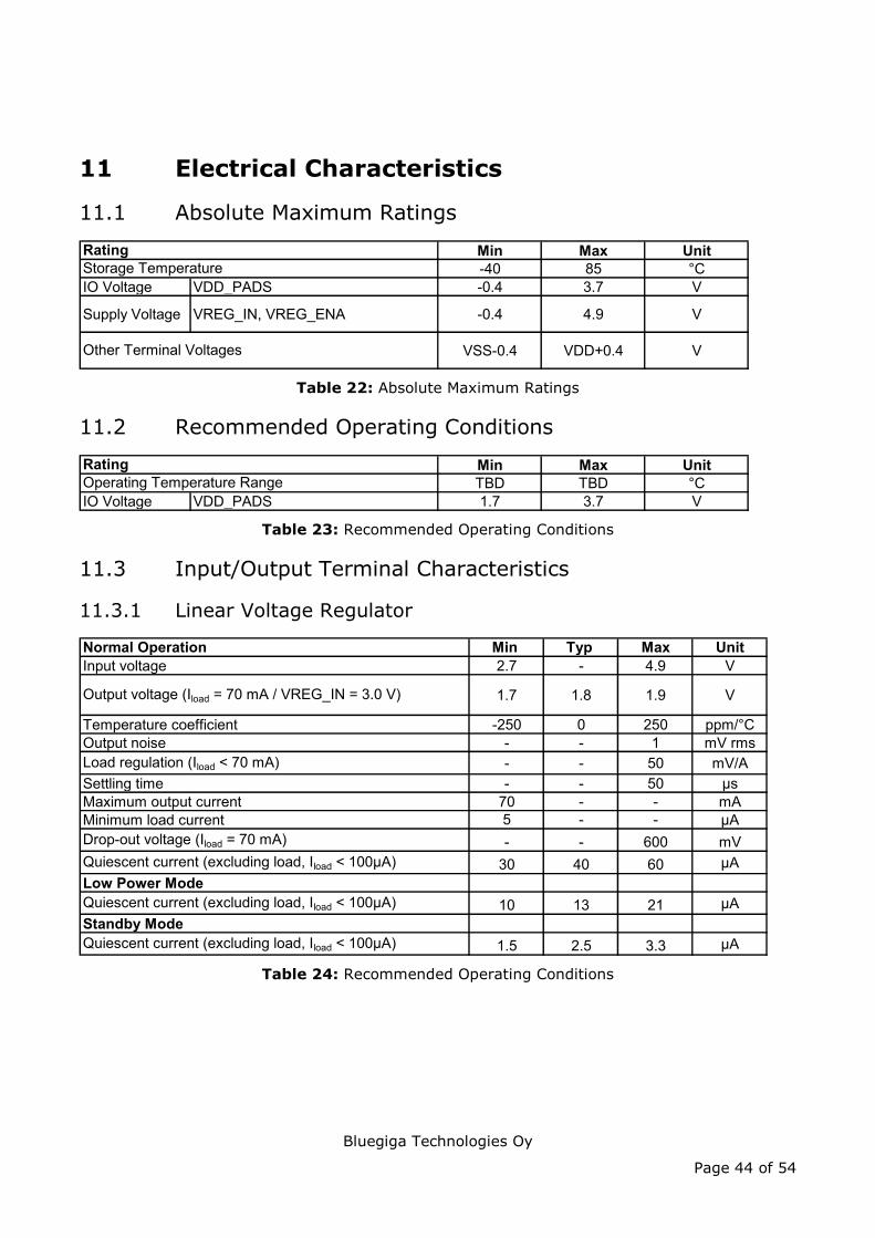
11 Electrical Characteristics
11.1 Absolute Maximum Ratings
Min Max Unit-40 85 °C
IO Voltage VDD_PADS -0.4 3.7 V
Supply Voltage VREG_IN, VREG_ENA -0.4 4.9 V
VSS-0.4 VDD+0.4 V
RatingStorage Temperature
Other Terminal Voltages
Table 22: Absolute Maximum Ratings
11.2 Recommended Operating Conditions
Min Max UnitTBD TBD °C
IO Voltage VDD_PADS 1.7 3.7 V
RatingOperating Temperature Range
Table 23: Recommended Operating Conditions
11.3 Input/Output Terminal Characteristics
11.3.1 Linear Voltage Regulator
Normal Operation Min Typ Max UnitInput voltage 2.7 - 4.9 V
Output voltage (Iload = 70 mA / VREG_IN = 3.0 V) 1.7 1.8 1.9 V
Temperature coefficient -250 0 250 ppm/°COutput noise - - 1 mV rmsLoad regulation (Iload < 70 mA) - - 50 mV/ASettling time - - 50 µsMaximum output current 70 - - mAMinimum load current 5 - - µADrop-out voltage (Iload = 70 mA) - - 600 mVQuiescent current (excluding load, Iload < 100µA) 30 40 60 µALow Power ModeQuiescent current (excluding load, Iload < 100µA) 10 13 21 µAStandby ModeQuiescent current (excluding load, Iload < 100µA) 1.5 2.5 3.3 µA
Table 24: Recommended Operating Conditions

Bluegiga Technologies Oy
Page 45 of 54
11.3.2 Digital
Digital Terminals Min Typ Max Unit
VIL input logic level low 1.7V ≤ VDD ≤ 3.6V -0.4 - 0.25xVDD VVIH input logic level high 1.7V ≤ VDD ≤ 3.6V 0.7VDD - VDD+0.3 V
VOL output logic level low 1.7V ≤ VDD ≤ 3.6V, (Io = 4.0 mA) - - 0.125 V
VOH output logic level high 1.7V ≤ VDD ≤ 3.6V, (Io = -4.0 mA) VDD-0.4 - VDD V
Strong pull-up -100 -40 -10 µAStrong pull-down 10 40 100 µAWeak pull-up -5 -1 -0.2 µAWeak pull-down 0.2 1 5 µAI/O pad leakage curren -1 0 1 µACl input capacitance 1 - 5 pF
Input Voltage Levels
Output voltage levels
Input Tri-state Current with:
Table 25: Digital terminal electrical characteristics
11.3.3 Reset
Power-on Reset Min Typ Max UnitVDD_CORE (a falling threshold 1.13 1.24 1.3 VVDD_CORE (a rising threshold 1.2 1.31 1.35 VHysteresis 0.05 0.07 0.15 V
(a VDD_CORE is a core voltage supplied by the internal 1.5 V voltage regulator. Table 26: Power on reset characteristics
11.3.4 32 kHz External Reference Clock
Min Nom MaxFrequency 32748 32768 32788 HzFrequency deviation @25°C - - 20 +/- ppm
Frequency deviation -25°C to 85°C - - 150 +/- ppm
Input high level Square wave 0.625xVDD_PADS - - VInput low level Square wave - - 0.425xVDD_PADS VDuty cycle Square wave 30 - 70 %Rise and fall time - - 50 ns
Integrated frequency jitter
Integrated over the band 200 Hz
to 15 kHz- - - Hz (rms)
UnitsParameter Conditions/Notes
Specifications
Table 27: External Reference Clock

Bluegiga Technologies Oy
Page 46 of 54
11.4 Power Consumption
Operation Mode Connection Type Average UnitPage scan, time interval 1.28s - 0.4 mAInquiry and page scan, time interval1,28s - 0.8 mAACL no trafic Master 4 mAACL with file transfer Master 9 mAACL 40ms sniff Master 2 mAACL 1,28s sniff Master 0.2 mAeSCO EV5 Master 12 mAeSCO EV3 Master 18 mAeSCO EV3 - hands-free - setting S1 Master 18.5 mASCO HV1 Master 37 mASCO HV3 Master 17 mASCO HV3 30ms sniff Master 17 mAACL no traffic Slave 14 mAACL with file transfer Slave 17 mAACL 40ms sniff Slave 1.6 mAACL 1.28s sniff Slave 0.2 mAeSCO EV5 Slave 19 mAeSCO EV3 Slave 23 mAeSCO EV3 - hands-free - setting S1 Slave 23 mASCO HV1 Slave 37 mASCO HV3 Slave 23 mASCO HV3 30ms sniff Slave 16 mAStandby host connection (Deep-Sleep) - 40 µAReset (active low) - 39 µA
Note: Conditions 20°C VREG_IN 3.15VVDD_PADS 3.15VUART BAUD rate 115.2 kbps
Table 28: Power Consumption
Bluegiga Technologies Oy
Page 47 of 54
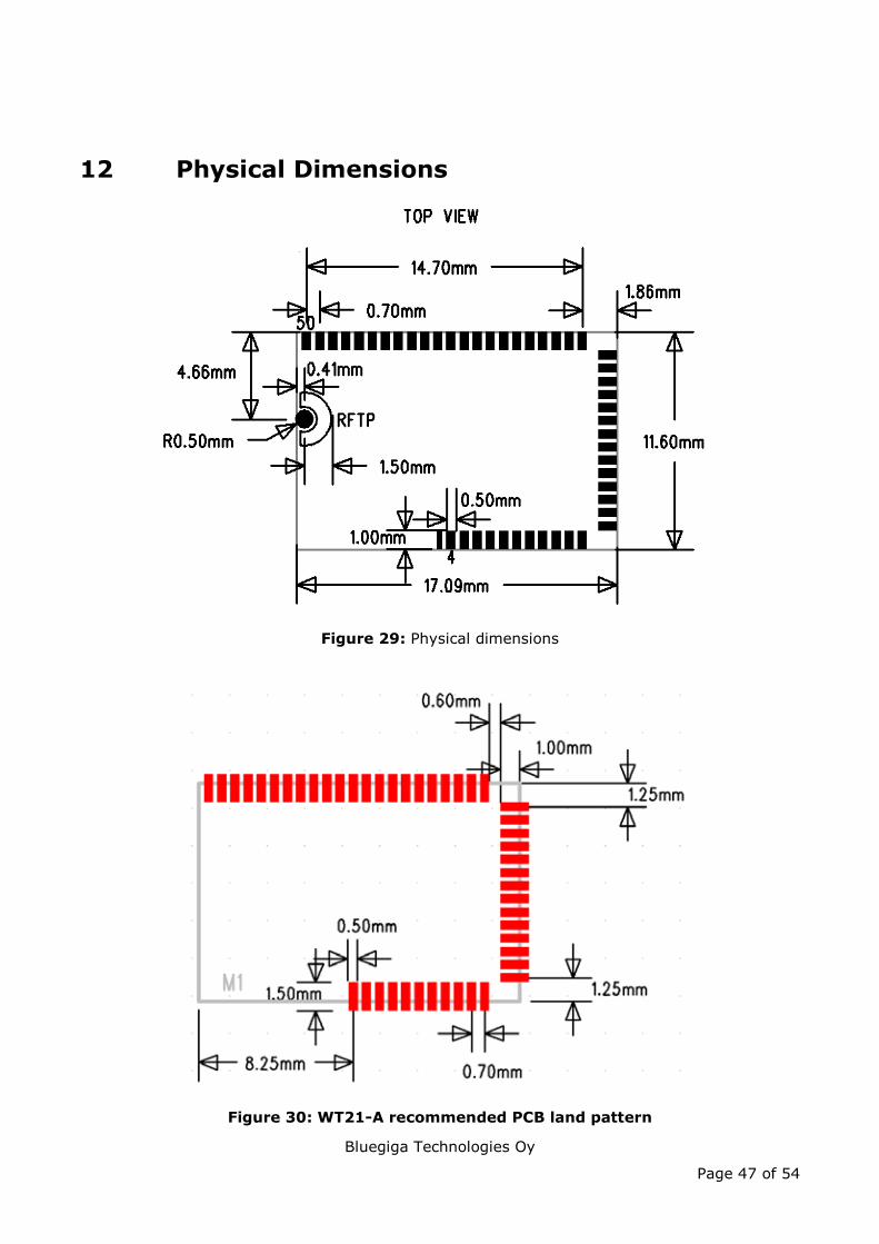
12 Physical Dimensions
Figure 29: Physical dimensions
Figure 30: WT21-A recommended PCB land pattern
Bluegiga Technologies Oy
Page 48 of 54
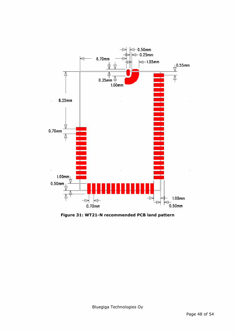
Figure 31: WT21-N recommended PCB land pattern
Bluegiga Technologies Oy
Page 49 of 54
2.5 mm
9.7 mm
17.1 mm
6.8 mm
2.2 mm
17.1 mm
9.7 mm
10.4 mm 11.6 mm
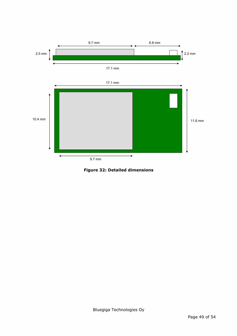
Figure 32: Detailed dimensions
Bluegiga Technologies Oy
Page 50 of 54
13 Layout Guidelines
13.1 WT21-N
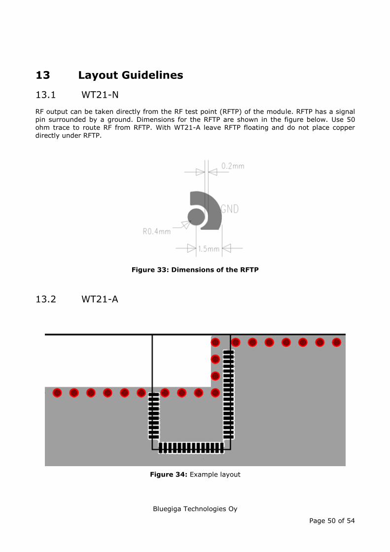
RF output can be taken directly from the RF test point (RFTP) of the module. RFTP has a signal pin surrounded by a ground. Dimensions for the RFTP are shown in the figure below. Use 50 ohm trace to route RF from RFTP. With WT21-A leave RFTP floating and do not place copper directly under RFTP.
Figure 33: Dimensions of the RFTP
13.2 WT21-A
Figure 34: Example layout
Bluegiga Technologies Oy
Page 51 of 54
Do not connect RFTP for WT21-A. See figure 32 for the recommended PCB land patern. The impedance matching of the antenna is design for the evaluation board of WT21. For an optimal performance of the antenna the layout should strictly follow the layout example shown in figure 31 and the thickness of FR4 should be 1,6 mm. Any dielectric material close to the antenna will change the resonant frequency and it is recommended not to place a plastic case or any other dielectric closer than 5 mm from the antenna. If this is not possible, or if using other thickness of FR4 than 1,6 mm, then the antenna can be retuned by removing extra FR4 under the antenna. Please, contact Bluegiga for the details.
Any metal in close proximity of the antenna will prevent the antenna to radiate freely. It is recommended not to place any metal closer than 20 mm from the antenna.
Following recommendations helps to avoid EMC problems arising in the design. Note that each design is unique and the following list do not consider all basic design rules such as avoiding capacitive coupling between signal lines. Following list is aimed to avoid EMC problems caused by RF part of the module.
Do not remove copper from the PCB more than needed. Use ground filling as much as possible. However remove small floating islands after copper pour.
Do not place a ground plane underneath the antenna. The grounding areas under the module should be designed as shown in Figure 31.
When using overlapping ground areas use conductive vias separated max. 3 mm apart at the edge of the ground areas. This prevents RF to penetrate inside the PCB. Use ground vias extensively all over the PCB. All the traces in (and on) the PCB are potential antennas.
Avoid loops. Ensure that signal lines have return paths as short as possible. With sensitive analog
signals, such as analog audio, use solid ground plane and make sure that the return path for the signal lines is low impedance and follows the signal lines all the way.

Bluegiga Technologies Oy
Page 52 of 54
14 Certifications WT21 is compliant to the following specifications.
14.1 Bluetooth
WT21 module is Bluetooth qualified and listed as a controller subsystem and it is Bluetooth compliant to the following profiles of the core spec version 2.1/2.1+EDR.
RF, Baseband, Link Manager, Host Controller Interface, Serial Port Profile and RFCOMM with TS 07.10.
Bluetooth QDID: B016019
14.2 FCC
This device complies with Part 15 of the FCC Rules. Operation is subject to the following two conditions:
(1) this device may not cause harmful interference, and
(2) this device must accept any interference received, including interference that may cause undesired operation.
FCC RF Radiation Exposure Statement: This equipment complies with FCC radiation exposure limits set forth for an uncontrolled environment. End users must follow the specific operating instructions for satisfying RF exposure compliance. This transmitter must not be co-located or operating in conjunction with any other antenna or transmitter. Note: When using WT21-A the end product must display an exterior label with the following detail incorporated: “Contains Transmitter Module FCC ID: QOQWT21A”
When using WT21-N the end product must display an exterior label with the following detail incorporated: “Contains Transmitter Module FCC ID: QOQWT21N”

Bluegiga Technologies Oy
Page 53 of 54
14.3 CE
WT21 meets the requirements of the standards below and hence fulfills the requirements of EMC Directive 89/336/EEC as amended by Directives 92/31/EEC and 93/68/EEC within CE marking requirement.
EMC (immunity only) EN 301 489-17 V.1.3.3 in accordance with EN 301 489-1 V1.8.1
Radiated emissions EN 300 328 V1.7.1
14.4 Industry Canada (IC)
WT21-A and WT21-N meets Industry Canada’s procedural and specification requirements for certification.
Industry Canada ID: 5123A-BGTWT21A
Industry Canada ID: 5123A-BGTWT21N
14.5 Qualified Antenna Types for WT21-N
This device has been designed to operate with the antennas listed below, and having a maximum gain of 2 dB. Antennas not included in this list or having a gain greater than 2 dB are strictly prohibited for use with this device. The required antenna impedance is 50 ohms.
Antenna Type Maximum GainDipole 2 dBi
Qualified Antenna Types for WT21-N
Table 29: Qualified Antenna Types for WT21-N
Any antenna that is of the same type and of equal or less directional gain as listed in table 29 can be used without a need for retesting. To reduce potential radio interference to other users, the antenna type and its gain should be so chosen that the equivalent isotropically radiated power (e.i.r.p.) is not more than that permitted for successful communication. Using an antenna of a different type or gain more than 2 dBi will require additional testing for FCC, CE and IC. Please, contact [email protected] for more information.

Bluegiga Technologies Oy
Page 54 of 54
15 Contact Information Sales: [email protected]
Technical support: [email protected]
http://www.bluegiga.com/techforum/
Orders: [email protected]
Head Office / Finland:
Phone: +358-9-4355 060
Fax: +358-9-4355 0660
Street Address:
Sinikalliontie 5A
02630 ESPOO
FINLAND
Postal address:
P.O. BOX 120
02631 ESPOO
FINLAND
Sales Office / USA:
Phone: (781) 556-1039
Bluegiga Technologies, Inc.
99 Derby Street, Suite 200 Hingham, MA 02043
AvnET EmBEddEd officES.
LocAL AvnET EmBEddEd BuSinESSES:
06/2010
www.avnet-embedded.eu
All trademarks and logos are the property of their respective owners. This document provides a brief overview only and is not intended to be complete or binding offer. Product information, including information related to a product‘s specifications, uses or conformance with legal or other requirements, is obtained by Avnet from its suppliers or other sources deemed reliable and is provided by Avnet on an „As Is“ basis. Avnet makes no representation as to the accuracy or completeness of the product information and Avnet disclaims all representations, warranties and liabilities under any theory with respect to the product information, including any implied warranties of merchantability, fitness for a particular purpose, title and/or non-refringement. All product information is subject to change without notice.
dEnmArkAvnet EmbeddedAvnet Nortec A/SEllekær 92730 HerlevPhone: +45 3678 6250Fax: +45 3678 [email protected]
finLAndAvnet EmbeddedAvnet Nortec OyTiilenpolttajankuja 3 A B1720 VantaaPhone: +358 207 499260Fax: +358 942 [email protected]
frAncEAvnet EmbeddedAvnet EMG France SAImmeuble 154, Parc Chene 25, allée du General Benoist69000 BronPhone: +33 4 72 81 02 30Fax: +33 4 72 81 02 [email protected]
Avnet EmbeddedAvnet EMG France SA4, rue de la CoutureBâtiment Milan, BP 20209 94518 Rungis Cedex Phone: +33 1 49 78 88 88 Fax: +33 1 49 78 88 89 [email protected]
Avnet EmbeddedAvnet EMG France SAZA la Hallerais le Semiramis2, allée du Communel35770 Vern sur SeichePhone: +33 2 99 77 37 02Fax: +33 2 99 77 33 [email protected]
GErmAnY (AuSTriA, cZEcH rEpuBLic, HunGArY, poLAnd, SWiTZErLAnd)Avnet EmbeddedAvnet EMG GmbHGruber Straße 60c85586 PoingPhone: +49 8121 775 500 Fax: +49 8121 775 [email protected]
Avnet EmbeddedAvnet EMG GmbHLötscher Weg 6641334 NettetalPhone: +49 8121 775 500Fax: +49 8121 775 [email protected]
iTALY (porTuGAL, SpAin)Avnet EmbeddedAvnet EMG Italy SRLVia Manzoni, 4420095 Cusano MilaninoPhone: +39 02 66092 1Fax: +39 02 66092 [email protected]
nETHErLAndS (BELGium, LuXEmBourG)Avnet EmbeddedAvnet B.V.Takkebijsters 24802 BL BredaPhone: +31 76 5722400Fax: +31 76 [email protected]
SWEdEn (norWAY)Avnet EmbeddedAvnet Nortec ABEsplanaden 3 D172 67 SundbybergPhone: +46 8 564 725 50Fax: +46 8 760 01 [email protected]
uniTEd kinGdom (irELAnd)Avnet EmbeddedAvnet EMG Ltd.Pilgrims Court, 15/17 West StreetReigate, Surrey, RH2 9BLPhone: +44 1737 227800Fax: +44 1737 [email protected]