Available online at: Performance of AHB Bus ... · Dynamic Multiresolution and Lossless Real Time...
6
© 2015, IJCERT All Rights Reserved Page | 1245 International Journal of Computer Engineering In Research Trends Volume 2, Issue 12, December-2015, pp. 1245-1250 ISSN (O): 2349-7084 Performance of AHB Bus Tracer with Dynamic Multiresolution and Lossless Real Time Compression 1 VELLANKI SATHEESH BABU, 2 B.N. SRINIVASA RAO 1 Pursuing M.Tech, VLSI DESIGN, Dept of ECE 2 Assistant Professor, Department of Electronics and Communication Engineering Avanthi Institute of Engineering and Technology, Visakhapatnam, Andhra Pradesh, India. Abstract- In this paper we demonstrate the On-Chip bus SoC(system-on-chip) infrastructure that connects major hardware components. Monitoring the on-chip bus signals is crucial to the SoC debugging and performance analysis/optimization. The past two decades of SoC evolution have seen an exponential increase in complexity. Today’s devices have multiple processing units, CPUs, GPUs, DSPs, DMAs, third-party IP blocks and custom logic. As if the hardware is not complicated enough, there will of course be substantial amounts of sophisticated software code running on the SoC hardware/software integration, and testing are made very much harder. The commercial consequences of problems in the development flow are potentially dire: since the debugging / analysis needs are adaptable: some designers need all signals at cycle-level, while some others only care about the transactions. For the latter case, tracing all signals at cycle-level wastes a lot of trace memory. Thus, there must be a way to capture traces at different abstraction levels based on the specific debugging/analysis need. Key words— SoC(system-on-chip), bus tracer, On-Chip, SoC debugging and analysis. —————————— —————————— 1. INTRODUCTION In many ways, the worst problems are those which do not produce an outright fault condition, but instead have a more subtle impact. The SoC may consume more power than expected; or perhaps, even though designed with substantial margins in the specification, it will deliver the minimum required data rate and no more. Getting a grip on all this complexity calls for a fundamental rethink in the way we do SoC development and debug. In particular, it requires robust analytical tools that give the development team actionable information on how the chip is operating as a system. Moreover, these tools need to be based on more than software instrumentation, piecemeal analysis of subsystems and legacy interfaces like JTAG.The solution is to build instrumentation, filtering and analytics capabilities into the hardware itself – yes, there is a penalty in terms of silicon real estate, but the benefits substantially outweigh the costs. By placing non-intrusive, simple but intelligent, configurable, blocks capable of monitoring buses or custom logic signals into the design, the development team will get to see how the design is really behaving, at wire speed. The SoC will be released faster (and with more commercial success); development cost and risk will be reduced; there will be fewer bugs in the field, and any issues that do occur will be identified and can be resolved more quickly. One way of achieving this change in paradigm is to employ a third-party suite of debug and performance analysis tools. It is possible to provide a fully message- based platform that enables concurrent access by multiple performance analysis tools in real-time. The architecture is highly modular and comprises of three Available online at: www.ijcert.org
-
Upload
nguyenlien -
Category
Documents
-
view
219 -
download
0
Transcript of Available online at: Performance of AHB Bus ... · Dynamic Multiresolution and Lossless Real Time...
© 2015, IJCERT All Rights Reserved Page | 1245
International Journal of Computer Engineering In Research Trends
Volume 2, Issue 12, December-2015, pp. 1245-1250 ISSN (O): 2349-7084
Performance of AHB Bus Tracer with Dynamic Multiresolution and Lossless Real
Time Compression
1 VELLANKI SATHEESH BABU,2
B.N. SRINIVASA RAO
1Pursuing M.Tech, VLSI DESIGN, Dept of ECE 2Assistant Professor, Department of Electronics and Communication Engineering
Avanthi Institute of Engineering and Technology, Visakhapatnam,
Andhra Pradesh, India.
Abstract- In this paper we demonstrate the On-Chip bus SoC(system-on-chip) infrastructure that connects major hardware components. Monitoring the on-chip bus signals is crucial to the SoC debugging and performance analysis/optimization. The past two decades of SoC evolution have seen an exponential increase in complexity. Today’s devices have multiple processing units, CPUs, GPUs, DSPs, DMAs, third-party IP blocks and custom logic. As if the hardware is not complicated enough, there will of course be substantial amounts of sophisticated software code running on the SoC hardware/software integration, and testing are made very much harder. The commercial consequences of problems in the development flow are potentially dire: since the debugging / analysis needs are adaptable: some designers need all signals at cycle-level, while some others only care about the transactions. For the latter case, tracing all signals at cycle-level wastes a lot of trace memory. Thus, there must be a way to capture traces at different abstraction levels based on the specific debugging/analysis need.
Key words— SoC(system-on-chip), bus tracer, On-Chip, SoC debugging and analysis.
—————————— ——————————
1. INTRODUCTION In many ways, the worst problems are those which do
not produce an outright fault condition, but instead
have a more subtle impact. The SoC may consume
more power than expected; or perhaps, even though
designed with substantial margins in the specification,
it will deliver the minimum required data rate and no
more.
Getting a grip on all this complexity calls for a
fundamental rethink in the way we do SoC
development and debug. In particular, it requires
robust analytical tools that give the development team
actionable information on how the chip is operating as
a system. Moreover, these tools need to be based on
more than software instrumentation, piecemeal
analysis of subsystems and legacy interfaces like
JTAG.The solution is to build instrumentation, filtering
and analytics capabilities into the hardware itself – yes,
there is a penalty in terms of silicon real estate, but the
benefits substantially outweigh the costs. By placing
non-intrusive, simple but intelligent, configurable,
blocks capable of monitoring buses or custom logic
signals into the design, the development team will get
to see how the design is really behaving, at wire speed.
The SoC will be released faster (and with more
commercial success); development cost and risk will be
reduced; there will be fewer bugs in the field, and any
issues that do occur will be identified and can be
resolved more quickly.
One way of achieving this change in paradigm is to
employ a third-party suite of debug and performance
analysis tools. It is possible to provide a fully message-
based platform that enables concurrent access by
multiple performance analysis tools in real-time. The
architecture is highly modular and comprises of three
Available online at: www.ijcert.org

Bindu Madhuri et al., International Journal of Computer Engineering In Research Trends Volume 2, Issue 12, December-2015, pp. 1245-1250
© 2016, IJCERT All Rights Reserved Page | 1246
classes of modules: advanced; message; and
communicators.
Advanced modules can be thought of as probes that
can be integrated into the system, for example, by
connecting to the block-level interfaces of system
components such as bus fabric links. Message modules
can be used to construct an on-chip message passing
fabric which is independent of the system interconnect.
Communicators interface the various components to
debug and performance tools, which can be outside of
the SoC.The Advanced Microcontroller Bus
Architecture (AMBA) specification defines an on-chip
communication standard for designing high-
performance embedded microcontrollers. The AHB
acts as the high-performance system backbone bus.
AHB supports the efficient connection of processors,
on-chip memories and off-chip external memory
interfaces with low-power peripheral macrocell
functions. AHB is also specified to ensure ease of use in
an efficient design flow using synthesis and automated
test techniques.
Fig 1.A Typical AMBA AHB based system
An AMBA AHB design may contain one or more bus
masters, typically a system would contain at least the
processor and test interface. However, it would also be
common for a Direct Memory Access (DMA) or Digital
Signal Processor (DSP) to be included as bus masters.
Figure3 is the bus tracer overview. It mainly contains
four parts: Event Generation Module, Abstraction
Module, Compression Modules, and Packing Module.
Event Generation Module controls the start/stop time,
the trace mode, and the trace depth of traces. This
information is sent to the following modules. Based on
the trace mode, the Abstraction Module abstracts the
signals in both timing dimension and signal dimension.
The abstracted data are further compressed by the
Compression Module to reduce the data size. Finally,
the compressed results are packed with proper headers
and written to the trace memory by the Packing
Module.
2. OBJECTIVES OF THE AMBA SPECIFICATION:
The AMBA specification has been derived to satisfy
four key requirements:
• To facilitate the right-first-time development of
embedded microcontroller products with one or more
CPUs or signal processors
• To be technology-independent and ensure that highly
reusable peripheral and system macro-cells can be
migrated across a diverse range of IC processes and be
appropriate for full-custom, standard cell and gate
array technologies
• To encourage modular system design to improve
processor independence, providing a development
road-map for advanced cached CPU cores and the
development of peripheral libraries
• To minimize the silicon infrastructure required to
support efficient on-chip and off-chip communication
for both operation and manufacturing test
2.1.A Typical AMBA-Based Microcontroller:
An AMBA-based microcontroller typically consists of a
high-performance system backbone bus (AMBA AHB
or AMBA ASB), able to sustain the external memory
bandwidth, on which the CPU, on-chip memory and
other Direct Memory Access (DMA) devices reside.
This bus provides a high-bandwidth interface between
the elements that are involved in the majority of
transfers. Also located on the high-performance bus is a
bridge to the lower bandwidth APB, where most of the
peripheral devices in the system are located.
2.1.1. Bus cycle:
A bus cycle is a basic unit of one bus clock period and
for the purpose of AMBA AHB or APB protocol
descriptions is defined from rising-edge to rising-edge
transitions. An ASB bus cycle is defined from falling-
edge to falling edge transitions. Bus signal timing is
referenced to the bus cycle clock.
2.1.2. Bus transfer:
An AMBA ASB or AHB bus transfer is a read or write
operation of a data object, which may take one or more
bus cycles. The bus transfer is terminated by a
completion response from the addressed slave.
2.1.3. Burst operation:
A burst operation is defined as one or more data
transactions, initiated by a bus master, which have a
consistent width of transaction to an incremental region
of address space. The increment step per transaction is
determined by the width of transfer (byte, half-word,

Bindu Madhuri et al., International Journal of Computer Engineering In Research Trends Volume 2, Issue 12, December-2015, pp. 1245-1250
© 2016, IJCERT All Rights Reserved Page | 1247
word). No burst operation is supported on the APB.A
typical AMBA AHB system design contains the
following components:
2.1.4. AHB master:
A bus master is able to initiate read and write
operations by providing an address and control
information. Only one bus master is allowed to actively
use the bus at any one time.
2.1.5. AHB slave:
A bus slave responds to a read or write operation
within a given address-space range. The bus slave
signals back to the active master the success, failure or
waiting of the data transfer.
3. AMBA BUS TRACER ARCHITECTURE
This section presents the architecture of our bus tracer.
Shown in Fig.1 is the bus tracer overview. It mainly
contains four parts 1)Event Generation Module
2)Abstraction Module 3)Compression Modules and 4)
Packing Module. The Event Generation Module
controls the start/stop time, the trace mode, and the
trace depth of traces. The signal Abstraction module
traces the corresponding AHB signals at proper time
according to user configuration. The trace compression
module compresses the trace data in accordance with
signal characteristics. Finally, in the data packing
module, the trace data is arranged compactly for
output to the internal on-chip trace memory or external
off- chip storage.
Fig.2.Multiresolution Bus Tracer Block Diagram
The transaction-level debugging provides software and
hardware designers a common abstraction level to
diagnose bugs. The abstraction level is in two
dimensions timing abstraction and signal abstraction.
The timing dimension has two abstraction levels which
are the cycle level and transaction. level. The cycle level
captures the signals at every cycle. The transaction
level records the signals only when their value changes.
The signal dimension involves grouping of AHB bus
signals into four categories: program address, data
address/value, access control signals (ACS), and
protocol control signals (PCS). Then, we define three
abstraction levels for those signals. The master state
level further abstracts the bus state level by only
recording the transfer activities of bus masters and
ignoring the handshaking activities within transactions.
This level also ignores the signals when the bus state is
IDLE, WAIT, and BUSY. The BSM is designed based on
the AMBA AHB 2.0 protocol to represent the key bus
handshaking activities within a transaction.
4. Post-T Tracer Architecture Overview:
It mainly contains four parts: 1. Event Generation
Module, 2. Abstraction Module, 3. Compression
Modules and 4. Packing Module.
4.1. Event Generation Module: The Event
Generation Module decides the beginning and ending
of a trace and its trace mode. Depending on the
combinations of address data and trace depth AHB
decides to change the event depending upon its trace
granularity and direction. The AHB checks all the
events based on AHB protocol checker
4.2. The Abstraction Module: monitors the AMBA
bus and selects/filters signals based on the abstraction
mode. The abstraction mechanism deals with the trace
granularity and trace depth. In abstraction mode we
provide five modes in different granularities. They are
Mode 1 (full signal, cycle level), Mode 2 (full signal,
transaction level), Mode 3(bus state, cycle level), Mode
4 (bus state, transaction level), and Mode 5 (master
state, transaction level).
Fig.3. timing abstraction level mechanism
At Mode 1, the tracer traces all bus signals step by step
so the detailed bus activities can be observed. At Mode
2, the tracer traces all signals only when their values are
differed. At Mode 3, the tracer uses the Bus State
Machine, such as NORMAL, IDLE, ERROR, and so on,

Bindu Madhuri et al., International Journal of Computer Engineering In Research Trends Volume 2, Issue 12, December-2015, pp. 1245-1250
© 2016, IJCERT All Rights Reserved Page | 1248
to represent bus transfer activities in cycle changing
level. Comparing to mode FC designers can observe the
bus handshaking states without analyzing the detail
signals. At Mode 4, the tracer uses bus state to
represent bus transfer activities in transaction level Our
bus tracer also supports dynamic mode change (DMC)
feature which allows designers to change the trace
mode dynamically in real-time.
4.3. Compression Module: The purpose of
Compression Module is to reduce the trace size. It
accepts the signals from the abstraction module. To
increase the number of levels pipe ling stages has been
indicated. Using pipe line stage it improves overall
capability of the systems
4.4. Packing Module: The Packing Module is the last
phase. It receives the compressed data from the
compression module, processes them, and writes them
to the trace memory.
5. RESULTS AND DISCUSSION
Now this chapter deals with the simulation and
synthesis results of the implemented On-Chip AHB
Bus Tracer with Real-time Compression and Multi-
resolution. Here Modelsim tool is used in order to
simulate the design and checks the functionality of the
design. Once the functional verification is done, the
design will be taken to the Xilinx tool for Synthesis
process and the net list generation.
5.1 SIMULATION RESULTS
5.1.1 MODE FC
Figure 4 Simulation results of Mode FC
Simulation results of On-Chip AHB Bus Tracer with
Mode FC (Mode Full Signal, Cycle by cycle) as shown
in Figure 4.Input signal for On-Chip AHB Bus Tracer
are AMBA-AHB Bus signals which includes program
address, Address /Data value and Control
signals(ACS,PCS).
5.1.2 MODE FT
Bindu Madhuri et al., International Journal of Computer Engineering In Research Trends Volume 2, Issue 12, December-2015, pp. 1245-1250
© 2016, IJCERT All Rights Reserved Page | 1249
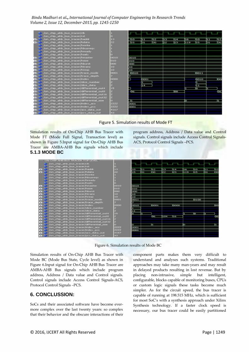
Figure 5. Simulation results of Mode FT
Simulation results of On-Chip AHB Bus Tracer with
Mode FT (Mode Full Signal, Transaction level) as
shown in Figure 5.Input signal for On-Chip AHB Bus
Tracer are AMBA-AHB Bus signals which include
program address, Address / Data value and Control
signals. Control signals include Access Control Signals-
ACS, Protocol Control Signals –PCS.
5.1.3 MODE BC
Figure 6. Simulation results of Mode BC
Simulation results of On-Chip AHB Bus Tracer with
Mode BC (Mode Bus State, Cycle level) as shown in
Figure 6.Input signal for On-Chip AHB Bus Tracer are
AMBA-AHB Bus signals which include program
address, Address / Data value and Control signals.
Control signals include Access Control Signals-ACS,
Protocol Control Signals –PCS.
6. CONCLUSSION:
SoCs and their associated software have become ever-
more complex over the last twenty years: so complex
that their behavior and the obscure interactions of their
component parts makes them very difficult to
understand and analyses such systems. Traditional
approaches may take many man-years and may result
in delayed products resulting in lost revenue. But by
placing non-intrusive, simple but intelligent,
configurable, blocks capable of monitoring buses, CPUs
or custom logic signals these tasks become much
simpler. As for the circuit speed, the bus tracer is
capable of running at 198.515 MHz, which is sufficient
for most SoC’s with a synthesis approach under Xilinx
Synthesis technology. If a faster clock speed is
necessary, our bus tracer could be easily partitioned
Bindu Madhuri et al., International Journal of Computer Engineering In Research Trends Volume 2, Issue 12, December-2015, pp. 1245-1250
© 2016, IJCERT All Rights Reserved Page | 1250
into more pipeline stages due to its streamlined
compression/packing processing flow.
REFERENCES:
[1+ ARM Ltd., San Jose, CA, “Embedded trace
macrocellarchitecture specification,” 2006.
*2+ B. Tabara and K. Hashmi, “Transaction-level
modeling and debug of SoCs,” presented at the IP SoC
Conf., France, 2004
*3+ ARM Ltd., San Jose, CA, “AMBA Specification (REV
2.0) ARMIHI0011A,” 1999.
*4+ ARM Ltd., San Jose, CA, “ARM. AMBA AHB Trace
Macrocell (HTM) technical reference manual ARM DDI
0328D,” 2007.
[5] J. Gaisler, E. Catovic, M. Isomaki, K. Glembo, and S.
Habinc, “GRLIB IP core user’s manual, gaisler
research,” 2009.
[6+ E. Rotenberg, S. Bennett, and J. E. Smith, “A trace
cache microarchitecture and evaluation,” IEEE Trans.
Comput., vol. 48, no. 1, pp. 111–120, Feb. 1999.
[7] A. B. T. Hopkins and K. D. Mcdonald-Maier,
“Debug support strategy for systems-on-chips with
multiple processor cores,” IEEE Trans. Comput., vol.
55, no. 1, pp. 174–184, Feb. 2006.
[8] B. Vermeulen, K. Goosen, R. van Steeden, and M.
Bennebroek, “Communication-centric SoC debug using
transactions,” in Proc. 12th IEEE Eur. Test Symp., May
20–24, 2007, pp. 69–76.
[9] Y.-T. Lin, C.-C. Wang, and I.-J. Huang, “AMBA
AHB bus protocol checker with efficient debugging
mechanism,” in Proc. IEEE Int. Symp. Circuits Syst.,
Seattle, WA, May 18–21, 2008, pp. 928–931
ABOUT AUTHORS
Name of the student: VELLANKI
SATHEESH BABU M-TECH
VLSI DESIGN (12811D5713)
Avanthi Institute of Engineering
and Technology, Visakhapatnam
jntuk,Completed B.tech (2008-
2012) ECE IN pulla reddy institute
of technology jntuh Hyderabad
B.N. Srinivasa Rao received his
B.Tech degree in Electronics and
Communication Engineering from
JNT University, Hyderabad, India and M.Tech in VLSI System Design
from JNT University, Hyderabad,
India. He is currently working as an Assistant Professor in Avanthi Institute of Engineering and
Technology, Visakhapatnam,Andhra Pradesh, India.
He has 6 years teaching and 9 years industrial
experience. He has 19 publications in various
International conferences and Journals. His area of
interest VLSI Semi and full custom design. He guided
many projects for B.Tech and M.Tech students.