Automotive Standard Analog Robustness and Performance · 5 Application schematics Featured...
40
Automotive Standard Anal og Robustness and Performance
Transcript of Automotive Standard Analog Robustness and Performance · 5 Application schematics Featured...

Automotive Standard AnalogRobustness and Performance
Content
Introduction .................................................................. 3Automotive grade qualification process ...................... 4Application schematics ............................................... 5Amplifiers and Comparators ........................................ 6Low-power operational amplifiers ........................................................... 6Precision operational amplifiers .............................................................. 8High output current & capacitive load operational amplifiers ....... 10Fast operational amplifiers ..................................................................... 12Comparators ............................................................................................ 14Grade 0 (150 °C) amplifiers and comparators.................................. 16
Current-sense amplifiers ............................................. 18DC-DC converters ....................................................... 19Conversion from car battery - synchronous ....................................... 19Conversion from car battery - asynchronous ..................................... 21Post-regulation .......................................................................................... 23
LED drivers .................................................................. 24LED array drivers ....................................................................................... 24LED row drivers .......................................................................................... 26
Linear Regulators (LDO) ............................................. 27LDO conversion from car batteries ....................................................... 27LDO post-regulation ................................................................................ 29
Logic ICs ..................................................................... 33Voltage references ..................................................... 34Watchdog, reset and supervisor ICs .......................... 35Current sensing for 48V batteries ............................... 36eDesignSuite ............................................................... 38Mobile apps ............................................................... 39ST Voltage regulators App ...................................................................... 39ST Op Amps App ...................................................................................... 39

3
IntroductionST provides a wide range of analog products dedicated to the challenging and demanding automotive market.
This brochure presents a large portfolio of ST’s products and solutions dedicated to voltage regulation, DC-DC conversion, signal amplification, current sensing, and LED driving as well as many other small analog ICs that are needed for today’s ever-growing automotive industry.
Thanks to innovative design techniques and a continuous focus on improving quality, ST offers high-performance devices that meet the specific requirements of the rigorous AEC-Q100 standard.
With a continuously growing portfolio offering the latest solutions in a wide variety of packages for powertrain, safety, and car-body systems to infotainment solutions, this brochure highlights the best products and solutions to help developers quickly get started with their designs as well as development tools for their day-to-day activities.
A large portfolio of products
For all automotive applications
Ampliers and comparators
Current-sense ampliers
DC-DC converters
LED drivers Linear regulators
Logic ICs Voltage references
Watchdog, reset, and
supervisor ICs

4
Automotive grade qualification process
Our automotive products meet the specific and rigorous requirements of the automotive market. This is the result of continuous quality and reliability improvements gained through our close collaboration with leading automotive suppliers and car makers. From product conception to delivery and beyond, our constant focus on learning and upgrading our quality processes, ensure we reach the highest level of excellence in the semiconductor industry.
Customer quality Change management Manufacturing & supply chain quality
Quality in product & technology development
Customer requirementsComplaint managementProduct return process
Product/Process Change NoticationsProduct Termination Notications
Non-conformity managementSupplier quality managementTraceability
Test owTechnology developmentProduct monitoring
Very high level of in-house parametric testing equipment
100% electrical testing with very extensive coverage coupled with automatic visual inspection
Part Average Testing (PAT) to detect and remove parts tested "pass" but potentially weak in reliability
Hot test & Junction Verication Test (JVT) at Final test for SOT23, Mini SO, SO, TSSOP, QFN/DFN
A specic commercial product number
COMPLIANCE WITH• IATF16949
• VDA 6.3
• AEC-Q100
• AEC-Q001
• AEC-Q002
PPAP provided
5
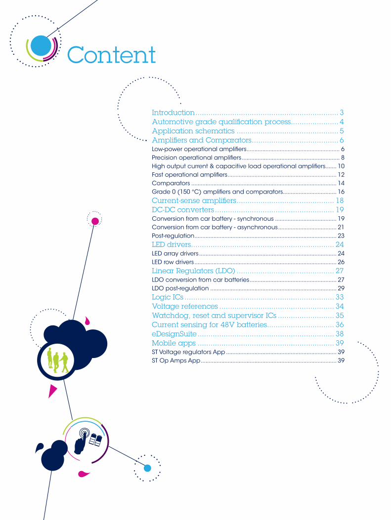
Application schematics
Featured products:
• TSX564IYPT
• TSX922IYDT
Steering angle sensor
+
-
R9cos
R10
R11
R3
R12
C6
C5
VrefC2R4Vref
in R5sin
R6
R7 R8
C4
C3
VrefB+
-
R1R2
C1
A
+
-
C
D
+
-
Featured products:
• TSX7191IYLT
• TSZ121IYLT
• TSX9291IYLT
Current measurement
R4
GND
Out
+
-
C1
R1
R3
R2Rshunt
Iload
Featured products:
• TSX922IYDT
• TSV912HYDT
Cylinder pressure sensor
Vcc/2
Out
+
-
C1
R1
Piezosensor
Featured products:
• TSU series
• TSX series
• TSV63 series
Photodiode current sensing
+
-
D
C
R
Featured products:
• TSZ124IYPT
Resistance temperature detector
C2
R10
R11
R9
R12
C1
D+-
R8
R7R6
R5
C+-
RTD
Vref R4 R3
R2R1
A+-
B+
-

6
Amplifiers & Comparators
0 5 10 15 20 25 30 350 5 10 15 20 25 30 35-70
-56
-42
-28
-14
0
14
28
42
56
70
-70
-56
-42
-28
-14
0
14
28
42
56
70
SourceVid=1V
SinkVid=-1V
T=-40°CT=25°CT=125°C
Vcc=36V
Outp
ut C
urre
nt (m
A)
Output Voltage (V)
4.0 8.0 12.0 16.0 20.0 24.0 28.0 32.0 36.04.0 8.0 12.0 16.0 20.0 24.0 28.0 32.0 36.0-1.4-1.2-1.0-0.8-0.6-0.4-0.20.00.20.40.60.81.01.21.4
-1.2
-0.8
-0.4
0.0
0.4
0.8
1.2
T=-40°C
Vicm=Vcc/2Vload=Vcc/2Rl=10kΩCl=100pF
T=125°C T=25°C
Slew
rate
(V/µ
s)
Supply Voltage (V)
FEATURES• Low-power consumption: 380 µA (typ.)
• Wide supply voltage: 4 to 36 V
• Rail-to-rail input and output
• Gain bandwidth product: 2.5 MHz
• Low input bias current: 30 nA (max.)
• No phase reversal
• High tolerance to ESD: 4 kV (HBM)
Slew rate vs. supply voltage and temperature
Output current vs. output voltage and temperature
LOW-POWER OPERATIONAL AMPLIFIERS
TSB572: low-power, 2.5 MHz, rail-to-rail input and output, 36 V operational amplifier
The TSB572 dual operational amplifier offers an extended voltage operating range from 4 to 36 V and rail-to-rail input/output. The TSB572 offers a very good speed/power consumption ratio with 2.5 MHz gain bandwidth product while consuming only
380 µA typically with a 36 V supply. The TSB572’s stability and robustness make it an ideal solution for applications with a wide voltage range.

77
Part number
Typ. ICC per
channel (µA)
Min. VCC (V)
Max. VCC (V)
Typ. GBP
(MHz)
Typ. SR (V/µs)
Max. VIO @ 25 °C
(µV)
Typ. IOUT(mA)
Rail to railPackage Single
Package Dual
Package Quad
In Out
TS931/2/4 20 2.7 10 0.1 0.05 10000 5 No Yes SOT23-5 (**) SO8 (**) SO14
TSZ121/2/4 31 1.8 5.5 0.4 0.19 5 17 Yes Yes
SOT23-5
SO8, MiniSO8
TSSOP14
TSV521A/2A/4A 45 2.7 5.5 1.15 0.89 600 55 Yes Yes MiniSO8
TSX631A/2A/4A (*) 45 3.3 16 0.2 0.12 500 90 Yes Yes MiniSO8
TSV631/2/4 60 1.5 5.5 0.88 0.34 500 69 Yes Yes SO8
TSB611 (*) 103 2.7 36 0.56 0.18 1000 60 No Yes NA
TSX561A/2A/4A (*) 250 3 16 0.9 1.1 600 90 Yes Yes MiniSO8 TSSOP14
TSB572 (*) 380 4 36 2.5 1 1500 60 Yes Yes NA MiniSO8 – QFN8 NA
TS912B/14A 400 2.7 16 1.4 1 2000 70 Yes Yes NA SO8 SO14
TS1871A/2A/4A 400 1.8 6 1.8 0.6 1000 72 Yes Yes
SOT23-5
SO8, TSSOP8 SO14, TSSOP14
TSV321A/358A/324A 500 2.5 6 1.4 0.6 1000 80 Yes Yes SO8, TSSOP8 SO14, TSSOP14
TS512A/14A 500 6 30 3 1.5 500 23 No No NA SO8 SO14 (**)
TS321A 600 3 30 0.8 0.4 2000 40 No No
SOT23-5
NA
NA
TSX711A/12 (*) 660 2.7 16 2.7 1.2 100 54 Yes Yes
SO8, MiniSO8TSX7191A/92 (*) 660 2.7 16 8.5 2.4 100 70 Yes Yes
TSZ181/2 (*) 700 2.2 5.5 3 4.7 25 27 Yes Yes
TSV911A/2A/4A 780 2.5 5.5 8 4.5 1500 35 Yes YesSOT23-5, SO8
SO8, MiniSO8 SO14, TSSOP14
TS507 850 2.7 5.5 1.9 0.6 100 115 Yes Yes SOT23-5 NA
TS9222/9224 900 2.7 12 4 1.3 500 80 Yes Yes NA SO8, TSSOP8 SO14, TSSOP14
TS951/2/4 950 2.7 12 3 1 6000 22 Yes Yes SOT23-5 SO8, MiniSO8 SO14, TSSOP14
(*): New products (**) Eligible for Automotive-grade qualification

8
PRECISION OPERATIONAL AMPLIFIERS
TSZ182: Very high accuracy (25 µV) zero drift 5V CMOS dual op amps with GBP = 3 MHz
The TSZ182 is a dual operational amplifier featuring very low offset voltages with virtually zero drift versus temperature changes.The TSZ182 offers rail-to-rail input and output, excellent speed/power consumption ratio, and 3 MHz gain bandwidth product, while consuming just 1 mA at 5 V. The device also features an ultra-low input bias current. These features make the TSZ182 ideal for high-accuracy high-bandwidth sensor interfaces.
FEATURES• Very high accuracy and stability: offset
voltage 25 µV (max.) at 25 °C, 35 µV over full temperature range (-40 to 125 °C)
• Rail-to-rail input and output
• Low supply voltage: 2.2 to 5.5 V
• Low power consumption: 1 mA (max.)at 5 V
• Gain bandwidth product: 3 MHz
• Slew rate of 4.7 V/µs
Supply Voltage (V)
Temperature (°C)
Input offset voltage vs. temperature for Vcc = 5 V
Positive slew rate vs. Supply voltage

99
Part number
Max. VIO
@ 25 °C(µV)
Typ. VIO drift
(µV/°C)
Max. IIB @ 25 °C (pA)
Min.VCC (V)
Max.VCC (V)
Typ. GBP
(MHz)
Typ. SR
(V/µs)
Typ. ICC per
channel (mA)
Typ. 1 kHz noise
(nV/√Hz)
Rail to railPackage Single
Package Dual
Package Quad
In Out
TSZ121/2/4 (*) 5 0.01 200 1.8 5.5 0.4 0.19 0.031 37 Yes Yes
SOT23-5
SO8, MiniSO8
TSSOP14
TSZ181/2 (*) 25 0.01 200 2.2 5.5 3 4.7 0.7 37 Yes Yes
NA
TSX711A/12 (*) 100 0.8 50 2.7 16 2.7 1.2 0.66 22 Yes Yes
TS507 100 1 70000 2.7 5.5 1.9 0.6 0.85 12 Yes Yes NA
TSX7191A/2 (*) 100 0.8 50 2.7 16 8.5 2.4 0.66 22 Yes Yes SO8, MiniSO8
TSB712 (*) 300 0.5 300000 2.7 36 6 3 1.8 12 Yes Yes
NA
SO8, MiniSO8
NA
TSB7192 (*) 300 0.5 300000 2.7 36 20 11 1.8 12 Yes Yes SO8, MiniSO8
TSV631A/2A/4A 500 2 10 1.5 5.5 0.88 0.34 0.06 60 Yes Yes SOT23-5 SO8 TSSOP14
TSV6391A/2A/4A 500 2 10 1.5 5.5 2.4 1.1 0.06 60 Yes YesSOT23-5
(**)SO8 (**) TSSOP14 (**)
TS9222/4 500 2 55000 2.7 12 4 1.3 0.9 9 Yes Yes NA SO8, TSSOP8 SO14, TSSOP14
TS512A/4A 500 2 150000 6 30 3 1.5 0.5 8 No No NA SO8 SO14 (**)
TSX561A/2A/4A (*) 600 2 100 3 16 0.9 1.1 0.25 48 Yes Yes
SOT23-5
MiniSO8 TSSOP14
TSX631A/2A/4A (*) 700 1 100 3.3 16 0.2 0.12 0.045 60 Yes Yes
TS9511 800 2 70000 2.7 12 3 1 0.95 25 Yes Yes NA
TSV851A/2A/4A 800 1 60000 2.3 5.5 1.3 0.7 0.13 30 No Yes SO8, MiniSO8 TSSOP14
LMV821A/2A/4A 800 1 120000 2.5 5.5 5.5 1.9 0.4 16 No Yes SO8, TSSOP8 SO14, TSSOP14
TS522/4 850 2 750000 5 30 15 7 2 4.5 No No NA SO8 (**) SO14 (**)
(*): New products (**) Eligible for Automotive-grade qualification

10
HIGH OUTPUT CURRENT & CAPACITIVE LOAD OPERATIONAL AMPLIFIERS
TSX561/2/4: high merit factor 16 V with large output drive operational amplifiers
The TSX561/2/4 and TSX561A/2A/4A series of operational amplifiers benefit from ST’s 16 V CMOS technology to offer state-of-the-art accuracy and performance in the smallest industrial packages. The TSX56 series offers an efficient speed/
power consumption ratio, 900 kHz gain bandwidth product while consuming only 250 μA at 16 V. Such features make the TSX56 series ideal for sensor interfaces and industrial signal conditioning. The wide temperature range and high ESD tolerance ease use in harsh automotive applications. .
FEATURES• Low power consumption:
235 μA (typ.) at 5 V
• Supply voltage: 3 to 16 V
• Gain bandwidth product: 900 kHz (typ.)
• Low input bias current: 1 pA (typ.)
• High tolerance to ESD: 4 kV
• 90 mA output current capability under 16 V
• Low offset voltage• “A” version: 600 μV (max.)• Standard version: 1 mV (max.)
1.5
1.0
0.5
0.0
-0.5
-1.0
Slew
rate
(V/µ
s)
-1.50.0 6.0 12.04.0 10.02.0 8.0
Vcc (V)14.0 16.0
T = 125 °C T = 25 °C T = -40 °C
Vicm = Vrl = Vcc/2Rl = 10 kΩ, Cl = 100 pF
Vin from 0.5 V to Vcc - 0.5 VSR calculated from 1 V to Vcc - 1 V
100
75
0
-25
-50
-75
Outp
ut c
urre
nt (m
A)
-1000.0 6.0 12.04.0 10.02.0 8.0
Output voltage (V)14.0 16.0
50
25
T = 125 °C T = 25 °C T = -40 °C
SinkVid = -1 V
SourceVid = 1 V
Output current vs. Output voltage and temperature
Positive slew rate vs. Supply voltage

1111
Part numberTyp. IOUT
(mA)Min. VCC
(V)Max. VCC
(V)Typ. GBP
(MHz)Typ. SR (V/µs)
Typ. ICC per channel
(mA)
Rail to railPackage Single
Package Dual
Package Quad
In Out
TS921/2/4 80 2.7 12 4 1.3 1 Yes Yes SO8 (**) SO8, TSSOP8 SO8, TSSOP14
TSX561A/2A/4A (*) 90 3 16 0.9 1.1 0.25 Yes Yes
SOT23-5
MiniSO8
TSSOP14
TSX631A/2A/4A (*) 90 3.3 16 0.2 0.12 0.045 Yes Yes TSSOP14
TS507 115 2.7 5.5 1.9 0.6 0.85 Yes Yes NA
TS982 200 2.5 5.5 2.2 0.7 5.5 Yes Yes NA SO8 NA
TSV321A/358A/324A 80 2.5 6 1.4 0.6 0.5 Yes Yes SOT23-5
SO8, TSSOP8 SO14, TSSOP14
TS9222/4 80 2.7 12 4 1.3 0.9 Yes Yes NA
(*): New products (**) Eligible for Automotive-grade qualification
STOp Amps

12
FAST OPERATIONAL AMPLIFIERS
TSX9291: high-speed 16 V rail-to-rail I/O CMOS operational amplifier
The TSX9291 and TSX9292 operational amplifiers offer excellent AC characteristics such as 16 MHz gain bandwidth, 27 V/μs slew rate, and 0.0003% THD+N. They are decompensated amplifiers which are stable when used with a gain higher than 2 or
lower than -1. The rail-to-rail input and output capability of these devices operates on a wide supply voltage range of 4 to 16 V. These last two features make the TSX929 series particularly well-adapted for a wide range of applications such as communications, I/V amplifiers for ADCs, and active filtering applications.
FEATURES• Rail-to-rail input and output
• Wide supply voltage: 4 to 16 V
• Gain bandwidth product: 16 MHz (typ.) at 16 V
• Low power consumption: 2.8 mA (typ.) at 16 V
• Slew rate: 27 V/μs
• Stable when used in gain configuration
• Low input bias current: 10 pA (typ.)
• High tolerance to ESD: 4 kV (HBM)
30
20
10
0
-10
Slew
Rat
e (V
/µs)
-20
-30
4 5 6Vcc (V)
7 8 9 10 1211 13 14 15 16
T = 125 °C T = 25 °C T = -40 °C
SR positive
SR negative
Vicm = VRI = Vcc/2RI = 10 kΩ, Cl = 20 pFVin from 0.5 V to Vcc -0.5 V
40
0
-20
-40
Gain
(dB)
Phas
e (°
)1 100010010
Frequency (kHz)10000
20
T = 125 °C T = 25 °C T = -40 °C
250
200
-100
-50
-150
-200
-250
100
150
50
0
Gain
Phase
Vicm = 8 V, G = 100Rl = 10 kΩ, Cl = 20 pF, Vrl = Vcc/2
Bode diagram vs. temperature for VCC = 16 V
Slew rate vs. Supply voltage and temperature

1313
Part numberTyp. GBP
(MHz)
Typ. SR
(V/µs)
Min.VCC (V)
Max.VCC (V)
Typ. ICC per
channel (mA)
Max. VIO
@ 25 °C
(µV)
Typ. 1 kHz noise (nV/√Hz)
Typ.IOUT (mA)
Rail to railPackage Single
Package Dual
Package Quad
In Out
TS921/2A/4A 4 1.3 2.7 12 1 900 9 80 Yes YesSO8 (**),
TSSOP8 (**)SO8, TSSOP8 SO14, TSSOP14
TL071/2/4 4 16 6 36 1.4 3000 15 40 No No SO8 SO8 SO14
TSB712 (*) 6 3 2.7 36 1.8 300 12 50 Yes Yes NA SO8, MiniSO8 NA
TSV911A/2A/4A 8 4.5 2.5 5.5 0.78 1500 27 35 Yes YesSOT23-5,
SO8
SO8, MiniSO8
SO14, TSSOP14
TSX7191/2 (*) 8.5 2.4 2.7 16 0.66 200 22 70 Yes Yes
SOT23-5
NA
TSX921/2 (*) 10 17.2 4 16 2.8 4000 16.5 62 Yes Yes
TS971/2/4 12 4 2.7 10 2 5000 4 100 No YesSO8, TSSOP8
DFN8 3x3TSSOP14
MC33078/9 15 7 5 30 2 2000 4.5 30 No No
NA
SO8 SO14
TS522/4 15 7 5 30 2 850 4.5 33 No No SO8 (**) SO14 (**)
TSX9291/2 (*) 16 26 4 16 2.8 4000 16.5 62 Yes Yes SOT23-5SO8 (**),
MiniSO8 (**)NA
TSV991A/2A/4A 20 10 2.5 5.5 0.82 1500 27 35 Yes Yes
SOT23-5, SO8
SO8, MiniSO8 SO14, TSSOP14
TSB7192 (*) 20 11 2.7 36 1.8 300 12 50 Yes Yes SO8, MiniSO8
NA
TSH80/2 65 115 4.5 12 8.2 10000 11 55 No Yes SO8
(*): New products (**) Eligible for Automotive-grade qualification

14
COMPARATORS
TSX3702/4: Micropower (5 µA) 16V dual/quad CMOS comparator with push-pull output
The TSX3702 and TSX3704 are micropower CMOS dual and quad voltage comparators which exhibit a very low current consumption of 5 µA (typ.) per comparator. Improving on the TS3704, these devices show a lower current consumption, a better
input offset voltage, and an enhanced ESD tolerance. The TSX3702 and TSX3704 are fully specified over a wide temperature range and are available in automotive grade for the TSSOP14 and SO8 packages. They are fully compatible with the TS3702 & TS3704 CMOS comparators and are available with similar packages.
FEATURES• Low supply current: 5 µA (typ.) per
comparator
• Wide single supply range 2.7 to 16 V or dual supplies (±1.35 to ±8 V)
• Extremely low input bias current: 1 pA (typ.)
• Input common-mode voltage range includes ground
• Push-pull output
• High input impedance: 1012 Ω (typ.)
• Fast response time: 2.7 µs (typ.) for 5 mV overdrive
• ESD tolerance: 4 kV (HBM), 200 V (MM)
Propagation delay vs supply voltage, overdrive = 100 mV
Propagation delay vs input signal overdrive @ VCC = 5V

1515
Part numberTyp. ICC per
channel (µA)
Min.VCC (V)
Max.VCC (V)
Typ. response time (ns) 100 mV
overdrive
Rail to rail In
Output type
Input typePackage Single
Package Dual
Package Quad
TS331/2/4 20 1.6 5 270 Yes Open drain BIP SOT23-5 SO8 SO14, TSSOP14
TSX3702/4 (*) 5 2.7 16 340 GND Push-pull
CMOS
NA
SO8 TSSOP14
TSX393/339 (*) 5 2.7 16 550 GND Open drain
NA
TS3011 470 2.2 5 8 Yes Push-pullDFN8 (2x2 mm, wettable flanks),
SOT23-5
TS3021/2 73 1.8 5 42 Yes Push-pull
BIP
SOT23-5 SO8, MiniSO8 NA
TS391 (*) 200 2 36 300 GNDOpen
collector
DFN8 (2x2 mm) (**)
SOT23-5NA
(*): New products (**) Eligible for Automotive-grade qualification

16
GRADE 0 (150 °C) AMPLIFIERS AND COMPARATORS
TSV912H: Wide-bandwidth (8 MHz), rail to rail input/output 5 V CMOS dual op amps
The TSV912H operational amplifier offers low-voltage operation and rail-to-rail input and output. The device features an excellent speed/power consumption ratio, offering an 8 MHz gain-bandwidth product while consuming only 1.1 mA (maximum) at 5 V. It
is unity gain stable and features an ultra-low input bias current. The TSV912H is a high-temperature version of the TSV912, and can operate from -40 to +150 °C with unique characteristics. Its main target applications are automotive, but the device is also ideal for sensor interfaces, battery-supplied and portable applications, as well as active filtering.
FEATURES• Rail-to-rail input and output
• Wide bandwidth
• Low power consumption: 820 µA (typ.)
• High output current: 35 mA
• Supply voltage: 2.5 to 5.5 V
• Low input bias current, 1 pA (typ.)
• Extended temperature range: -40 to + 150 °C
• ESD internal protection ≥ 5 kV (HBM)
• SO8 package
4
3
2
1Posi
tive
Slew
rate
(V/µ
s)
02.5 4.03.5 5.03.0 4.5
Supply voltage (V)5.5
T = 125 °C T = 25 °C T = -40 °CT = 150 °C
Vin: from 0.5 V to Vcc -0.5 VSR: calculated from 10% to 90%
400
300
200
100
Quan
tity
of p
arts
0-2.0 -0.5 1.0-1.0 0.5-1.5 0.0
Input offset voltage (mV)1.5 2.0
Vcc = 5 VVicm = 2.5 V
Tamb = 150 °C
Input offset voltage distribution at T = 150 °C
Positive slew rate

1717
Part numberMax. operating Temperature
(°C)
Typ. GBP (MHz)
Typ. SR (V/µs)
Min. VCC (V) Max. VCC (V)Typ. ICC per
channel (mA)
Rail to railPackage Dual
In Out
LM2904AH/WH 150 1.1 0.6 3 30 0.5 GND No TSSOP8, SO8, Mini-SO8 •
TSV912H 150 8 4.5 2.5 5.5 0.82 Yes Yes SO8 •
Part numberMax. operating Temperature
(°C)
Typ. ICC per
channel (µA)
Min. VCC (V)
Max. VCC (V)
Typ. response time (ns) 100 mV
overdriveRail to rail In Output type
Package Single
Package Dual
Package Quad
TS3021H 150 73 1.8 5 42 Yes Push-pull SOT23-5 NA NA
LM2903H/1H 150 200 2 36 300 GND Open collector NASO8,
TSSOP8SO14
High-temperature amplifiers
High-temperature comparators
MAIN APPLICATIONS
In-gearbox modulesEngine control Safety-critical systems
18
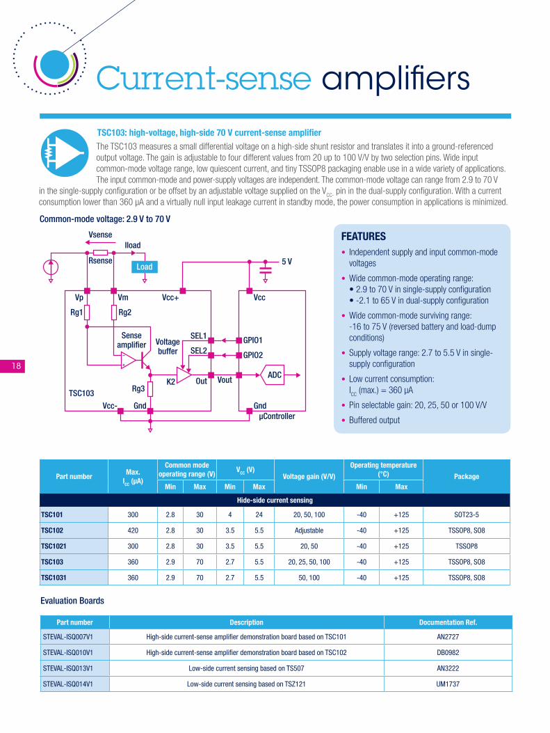
Current-sense amplifiers
Rsense
Iload
+
-
Rg2Rg1
TSC103 Rg3K2
Gnd GndµController
VmVp
Senseamplifier Voltage
buffer
Vcc-
Vcc+
SEL1 GPIO1
GPIO2
Vout
SEL2
Out
Vcc
5 V
Vsense
Load
ADC
FEATURES• Independent supply and input common-mode
voltages
• Wide common-mode operating range: • 2.9 to 70 V in single-supply configuration • -2.1 to 65 V in dual-supply configuration
• Wide common-mode surviving range: -16 to 75 V (reversed battery and load-dump conditions)
• Supply voltage range: 2.7 to 5.5 V in single-supply configuration
• Low current consumption: ICC
(max.) = 360 μA
• Pin selectable gain: 20, 25, 50 or 100 V/V
• Buffered output
Common-mode voltage: 2.9 V to 70 V
TSC103: high-voltage, high-side 70 V current-sense amplifier
The TSC103 measures a small differential voltage on a high-side shunt resistor and translates it into a ground-referenced output voltage. The gain is adjustable to four different values from 20 up to 100 V/V by two selection pins. Wide input common-mode voltage range, low quiescent current, and tiny TSSOP8 packaging enable use in a wide variety of applications. The input common-mode and power-supply voltages are independent. The common-mode voltage can range from 2.9 to 70 V
in the single-supply configuration or be offset by an adjustable voltage supplied on the VCC-
pin in the dual-supply configuration. With a current consumption lower than 360 μA and a virtually null input leakage current in standby mode, the power consumption in applications is minimized.
Part numberMax.
ICC (µA)
Common mode operating range (V)
VCC (V)Voltage gain (V/V)
Operating temperature (°C) Package
Min Max Min Max Min Max
Hide-side current sensing
TSC101 300 2.8 30 4 24 20, 50, 100 -40 +125 SOT23-5
TSC102 420 2.8 30 3.5 5.5 Adjustable -40 +125 TSSOP8, SO8
TSC1021 300 2.8 30 3.5 5.5 20, 50 -40 +125 TSSOP8
TSC103 360 2.9 70 2.7 5.5 20, 25, 50, 100 -40 +125 TSSOP8, SO8
TSC1031 360 2.9 70 2.7 5.5 50, 100 -40 +125 TSSOP8, SO8
Evaluation Boards
Part number Description Documentation Ref.
STEVAL-ISQ007V1 High-side current-sense amplifier demonstration board based on TSC101 AN2727
STEVAL-ISQ010V1 High-side current-sense amplifier demonstration board based on TSC102 DB0982
STEVAL-ISQ013V1 Low-side current sensing based on TS507 AN3222
STEVAL-ISQ014V1 Low-side current sensing based on TSZ121 UM1737

19
DC-DC convertersCONVERSION FROM CAR BATTERY - SYNCHRONOUSA6985F, A6986F and A6986: 38 V 0.5, 1.5 and 2A synchronous step-down switching regulators with 30 µA quiescent current The A6985F, A6986F and A6986 are step-down monolithic converters with synchronous rectification capable of 0.5, 1.5 and 2 A output current respectively. The output voltage adjustability ranges from 0.85 V to V
IN. The PMOS high side allows for
true 100% duty cycle capability and the wide input voltage range meet the cold crank and load dump needs for automotive systems. The “Low Consumption Mode” (LCM) is designed for applications active during car parking, so it maximizes the efficiency at light-load with controlled output voltage ripple. The “Low Noise Mode” (LNM) makes the switching frequency constant and minimizes the output voltage ripple overload current range, meeting low-noise requirements for applications such as car audio systems. The output voltage supervisor manages the reset phase for any digital load (MCU, FPGA). The RST open collector output can also implement output voltage sequencing during the power-up phase. The synchronous rectification, designed for high efficiency at medium to heavy loads, and the high switching frequency capability make the size of the application compact. Pulse-by-pulse current sensing on both power elements implements an effective constant current protection. The thermally performant HTSSOP 16 package allows for a typical junction to ambient resistance of 40 °C/W.
FEATURES• Input voltage: 4 to 38 V
• Output voltage: Fixed output voltage : 3.3 and 5 V or adjustable from 0.85 V to V
IN
• Output current: • 2 A for the A6986 • 1.5 A for the A6986F • 0.5 A for the A6985F
• Adjustable switching frequency (250 kHz – 2 MHz) + Sync. capability
• Synchronous rectification
• PMOS high-side for 100 % duty cycle
• Low minimum tON
(80 ns for A6985F/6F/6H)
• Dynamically adjustable skip current level in LCM (A6985F/6F/6H)
• Low Consumption Mode (IQ = 30 μA) or Low Noise Mode
• Inhibit & low shut-down current (8 μA)
• Power Good with adj. delay (embedded voltage supervisor to reset MCU)
• Adjustable soft start
• VBIAS to improve efficiency at light loads
• Ceramic COUT
allowed
• Over-current, over-voltage, and thermal protections
• HTSSOP16 package
Typical A6986F application diagram
VIN
PGND
PGND
MLF
VCC
SS/INH
DELAY
FSW SGND
signal GND
220p
75k
6.8uH
1MuC RST
VOUT
GND
20uF
PWR gnd
PWR gnd
10nF
68nF
470nF
10uF 1uF
EP SYNCH
COMP
FB
LX
LX
VBIAS
RST
A6986F

20
Part number VIN (V) VOUT (V) IOUT (A) Frequency IQ (µA) Other features Package
A6986
4 to 38
Adj. (0.85 - VIN) 2250 kHz to
2 MHz30
Synchronization, Adj. fSW, Adj. Soft-Start, Adj. reset, LNM/LCM
HTSSOP16
A6986FAdj. (0.85 - V
IN) 5
3.31.5
250 kHz to 2 MHz
30Synchronization, Adj. fSW, Adj. Soft-Start, Adj. reset,
LNM/LCM, Adj. ISKIP
HTSSOP16
A6985FAdj. (0.85 - VIN)
5 3.3
0.5250 kHz to
2 MHz30
Synchronization, Adj. fSW, Adj. Soft-Start, Adj. reset, LNM/LCM, Adj. ISKIP
HTSSOP16
A6984 4.5 to 36Adj. (0.9 - VIN)
3.30.4
250 kHz to 600 kHz
80 Adj. fSW, Internal Soft-Start, PGOOD, LNM/LCMQFN10
(4x4 mm with wettable flanks)
Evaluation Boards
Part number Description Documentation Ref.
STEVAL-ISA158V1 38 V, 2 A synchronous step-down switching regulator evaluation board based on A6986 DB2477
STEVAL-ISA185V1 38 V, 0.5 A synchronous step-down switching regulator evaluation board based on A6985F3V3 DB2814
STEVAL-ISA186V1 38 V, 0.5 A synchronous step-down switching regulator evaluation board based on A6985F5V DB2820
STEVAL-ISA187V1 38 V, 0.5 A synchronous step-down switching regulator evaluation board based on A6985F DB2823
STEVAL-ISA188V1 38 V, 1.5 A synchronous step-down switching regulator evaluation board based on A6986F3V3 DB2829
STEVAL-ISA189V1 38 V, 1.5 A synchronous step-down switching regulator evaluation board based on A6986F5V DB2831
STEVAL-ISA190V1 38 V, 1.5 A synchronous step-down switching regulator evaluation board based on A6986F DB2932
STEVAL-ISA200V1 High-efficiency synchronous step-down regulator based on A6984 DB3249
0.001 0.0120
30
40
50
60
70
80
0.1
A6986F VIN =13.5 VOUT = 3V3 VBIAS ISKIPL
A6986F VIN =13.5 VOUT = 3V3 NOVBIAS ISKIPH
A6986F VIN =13.5 VOUT = 3V3 NOVBIAS ISKIPL
A6986F VIN =13.5 VOUT = 3V3 VBIAS ISKIPH
A6986F VIN =13.5 VOUT = 3V3 VBIAS NOISKIP
A6986F VIN =13.5 VOUT = 3V3 NOVBIAS NOISKIP
Light-load efficiency A6986F5V at different ISKIP VIN = 13.5 V, VOUT = 5 V, fSW = 500 kHz
0 0.2
95
90
85
80
75
70
65
600.4 0.6 0.8 1 1.2 1.4 1.6
A6986F VIN =13.5 VOUT = 5 V VBIAS ISKIPL
A6986F VIN =13.5 VOUT = 5 V NOVBIAS ISKIPH
A6986F VIN =13.5 VOUT = 5 V NOVBIAS ISKIPL
A6986F VIN =13.5 VOUT = 5 V VBIAS ISKIPH
A6986F VIN =13.5 VOUT = 5 V NOVBIAS NOISKIP
A6986F VIN =13.5 VOUT = 5 V VBIAS NOISKIP
Efficiency curves for A6986F VIN = 13.5 V, VOUT = 5 V, fSW = 500 kHz

21
CONVERSION FROM CAR BATTERY - ASYNCHRONOUS
A7985A/6A: 2 A and 3 A step-down switching regulator for automotive applications
The A7986A is a step-down switching regulator with a 3.7 A (min.) current limited embedded power MOSFET, so it is able to deliver up to 3 A current to the load depending on application conditions. The input voltage can range from 4.5 to 38 V, while the
output voltage can be set starting from 0.6 V to VIN. Requiring a minimum set of external components, the device includes an internal 250 kHz
switching frequency oscillator that can be externally adjusted up to 1 MHz. The HSOP8 package with exposed pad allows for a junction to ambient resistance of 40 °C/W.
FEATURES• Output current: 3 A DC
• Input voltage : 4.5 to 38 V
• Output voltage adjustable from 0.6 V
A7986A buck topology application circuit
505560657075808590
0 0.5 1 1.5 2 2.5 3
Effic
ienc
y %
Output current [A]
12V18V24V
50.5
1
1.5
2
2.5
10 15 20 25 30 35
I º [A]
Vin [V]
Efficiency vs output current VOUT = 5 V
Maximum output current in Buck-Boost topology with A7986A, VOUT = 12 V
VINVIN
GNDGND
VOUT
GNDGND
SYNCSYNC
OUTOUT11
VCCVCC88
FSWFSW66
GNDGND99
ENEN33
COMPCOMP44
GNDGND77
FBFB55
SYNCSYNC22
• 250 kHz switching frequency, programmable up to 1 MHz
• Internal soft-start and enable pin
• Low dropout operation: 100% duty cycle
• Voltage feed-forward
• Zero- load current operation
• Over-current and thermal protection
• HSOP8 package

22
Typical A7986A positive buck-boost topology application
Part number VIN (V) VOUT (V) IOUT (A) Frequency Other features Package
A5970AD
4 to 36
Adj. (1.235 to VIN) 1 500 kHz Synchronization, VREF SO8
A5970D Adj. (1.235 to VIN) 1 250 kHz Synchronization, VREF SO8
A5972D Adj. (1.235 to VIN) 1.5 250 kHz Synchronization, VREF SO8
A5973AD Adj. (1.235 to VIN) 1.5 500 kHz Synchronization, VREF HSOP8
A5973D Adj. (1.235 to 35) 2 250 kHz Synchronization, VREF HSOP8
B5973D Adj. (1.235 to 35) 2 250 kHz Synchronization, VREF, Burn-in HSOP8
A5974AD Adj. (1.235 to 35) 2 500 kHz Synchronization, VREF HSOP8
A5974D Adj. (1.235 to 35) 2.5 250 kHz Synchronization, VREF HSOP8
A5975AD Adj. (1.235 to 35) 2.5 500 kHz Synchronization, VREF HSOP8
A5975D Adj. (1.235 to 35) 3 250 kHz Synchronization, VREF HSOP8
A6902D 8 to 36 Adj. (1.235 to 35) 1 250 kHz Synchronization, VREF, constant current with HS Sense SO8
A7985A4.5 to 38
Adj. (0.6 to 38) 2250 kHz to
1 MHzSynchronization, adj. fSW, Internal Soft-Start HSOP8
A7986A Adj. (0.6 to 38) 3250 kHz to
1 MHzSynchronization, adj. fSW, Internal Soft-Start HSOP8
A7987L (*) 4.5 to 61 Adj. (0.8 to VIN) 2250 kHz to 1.5 MHz
Synchronization, adj. fSW, Power Good signal, adj. soft-start, adj. current limit
HTSSOP16
A7987 (*) 4.5 to 61 Adj. (0.8 to VIN) 3250 kHz to 1.5 MHz
Synchronization, adj. fSW, Power Good signal, adj. SS, adj. current limit
HTSSOP16
(*): Products in development
Evaluation Boards
Part number Description Documentation Ref.
STEVAL-ISA088V1 1 A step down switching regulator (VIN =4 to 36 V, VOUT = 1.235 V to VIN) based on A5970D DB1265
STEVAL-ISA089V1 1.5 A step down switching regulator (VIN =4 to 36 V, VOUT = 1.235 V to VIN) based on A5972D DB1267
STEVAL-ISA106V1 1.5 A step-down switching regulator based on the A5973AD DB1716
STEVAL-ISA101V1 2 A DC step-down switching regulator with 4 to 36 V input voltage range based on the A5973D DB1663
STEVAL-ISA098V1 2 A step-down switching demonstration board based on the A7985A in HSOP8 package DB1621
STEVAL-ISA100V1 3 A step-down switching demonstration board based on the A7986A in HSOP8 package DB1623
STEVAL-ISA155V1 1 A constant current battery charger evaluation board based on the A6902D DB2340
STEVAL-ISA198V1 2 A step down DC - DC switching regulator (VIN = 4.5 to 60 V) based on the A7987L DB3109
STEVAL-ISA152V1 3.3 V / 3 A high efficiency step down DC-DC converter (VIN= 4.5 to 60 V) based on the A7987 DB2108
8VCC
7GND
FSW 6FB 5
1
2
3
4
OUT
SYNC
EN
COMP9TP
A7986A
VIN VOUT
C1
C4R4
C5
R2 2.49k
R1 47k
L1 15µH
D1C2 47µF
D2 STPS3L40U
M1
R5
R3 220
C3 2.2nF
C6
GND GND
R8
470pF
1.5k 100nF
0.1µF
10µF
1k
110k
STPS3L40U
STN3NF06L

23
POST-REGULATION
AST1S31HF: Up to 4 V, 3 A step-down 2.3 MHz switching regulator for automotive applications
The AST1S31HF is an internally compensated 2.3 MHz fixed frequency PWM synchronous stepdown regulator. The AST1S31HF operates from 2.8 to 4 V input, while it regulates an output voltage as low as 0.8 V and up to V
IN. The AST1S31HF device
integrates a 70 mΩ high-side switch and a 55 mΩ synchronous rectifier allowing very high efficiency with very low output voltages. The peak current mode control with internal compensation deliver a very compact solution with a minimum component count. The AST1S31HF is available in a 3 x 3 mm, 8-lead VFDFPN package.
FEATURES• Input voltage: 2.8 to 4 V
• Output voltage: 0.8 V to VIN
• Output current: 3 A
• Switching frequency: • 1.5 MHz (AST1S31) • 2.3 MHz (AST1S31HF)
• Synchronous rectification
• (HS: 60 mΩ; LS: 45 mΩ)
• Internal compensation
• Power Good signal
• Enable pin
• Internal Soft Start
• Ceramic COUT
allowed
• Over-current and thermal protections
• Packages: 8-lead DFN (3x3 mm)
-0.6
-0.4
-0.2
0
0.2
0.4
0.6
0 0.5 1 1.5 2 2.5 3
Load
regu
latio
n [%
]
Output current [A]
Vout = 1.8V
Vout = 1.2V
0
10
20
30
40
50
60
70
80
90
100
0 0.5 1 1.5 2 2.5 3
Effic
ienc
y [%
]
Output current [A]
Vout = 1.2V
Vout = 1.8V
Vout = 2.5V
Efficiency curves VIN = 3.3 V
Load regulation VIN = 3.3 V
Part number VIN (V) VOUT (V) IOUT (A) Frequency Iq Package Topology Other Features
AST1S31 2.8 to 4 0.8 to VIN 3 1.5 MHz 630 µADFN8
3 x 3 mmMonolithic
synchronousInternal comp, Soft-start,
Power Good
AST1S31HF 2.8 to 4 0.8 to VIN 3 2.3 MHz 630 µADFN8
3 x 3 mmMonolithic
synchronousInternal comp, Soft-start,
Power Good
A6727 5 to 12 0.8 to VIN > 6 300 kHz 6 mA SO8Synchronous
controllerAdj. OCB
Evaluation Boards
Part number Description Documentation Ref.
STEVAL-ISA069V1 3 A / 1.5 MHz step-down synchronous switching regulator based on the AST1S31 in 3x3 mm DFN package DB1572
STEVAL-ISA160V1 3 A / 2.3 MHz step-down synchronous switching regulator based on the AST1S31HF in 3x3 mm DFN package DB2858

24
LED Drivers
STAP16DPS05 block schematic
LED ARRAY DRIVERSSTAP16DPS05: 16-bit constant LED driver with output error detection and auto power-saving The STAP16DPS05 is a monolithic, low voltage, low current power 16-bit shift register designed for LED panel displays. The device contains a 16-bit serial-in, parallel-out shift register that feeds a 16-bit D-type storage register. In the output stage, sixteen regulated current sources are designed to provide 5 to 100 mA constant current to drive the LEDs.
FEATURES• Power supply voltage: 3 to 5.5 V
• 16 constant current output channels
• Adjustable output current through external resistor
• Short and open output error detection
• Serial data In/parallel data OUT
• 3.3 V micro driver-able
• Output current: 5 to 100 mA
• Auto power-saving
• Max. clock frequency: 30 MHz
• 20 V current generator rated voltage
• Thermal shutdown for over temperature protection
• ESD protection: 2.0 kV (HBM)
MAIN APPLICATIONS
Current ref
UVLOand POR
16 o
utpu
t cha
nnel
s
Thermalshutdown
SDI
SD0
CLKLE/DM1
VDOGND
R-EXT
OUT0OUT1
OUT2
OUT14
OUT15
Errordetection
Turn ON/OFF
OE/DM2
Control logic and data registers
Car exterior / interior lighting
Car rear light Clusters/ Instrumentation
Dashboard and Infotainment backlighting

2525
Part numberNb. of
channelsVIN (V) VOUT (V)
LED current
per channel
(mA)
Special featuresAuto
Power saving
Package
ALED1262XT 12 5.5 to 38 0 to 19 6 – 6012-channel LED drivers with open detection, 7-bit
local dimming brightness control, configurable bus-driven and stand-alone operation mode
NoTSSOP24
Exposed pad
ALED1642GWXTTR 16 3 to 5.5 0 to 20 3 – 40
7-bit current programmability, 12/16-bit grayscale control for brightness adjustment,
current setting through external resistor, programmable turn on/off, auto wake-up mode, open/shorted LED & temperature fault detection modes. Up to 30 MHz (max.) clock frequency
YesTSSOP14
Exposed pad
ALED8102S 8 3 to 5.5 0 to 20 5 – 100
8-channel LED drivers with constant current output channels up to 100 mA, controlled by
four switch inputs for local dimming and output enable pin for global dimming.
No TSSOP16
STAP08DP05XTTR 8 3 to 5.5 0 to 20 5 – 100 Short, open line & thermal shutdown protections. Output current adjustment through external
resistor. Serial data In. Up to 30 MHz (max.) clock frequency
NoTSSOP16
Exposed PAD
STAP16DPPS05XTTR 16 3 to 5.5 0 to 20 3 - 40 Yes TSSOP24 Exposed padSTAP16DPS05XTTR 16 3 to 5.5 0 to 20 5 – 100 Yes
Evaluation Boards
Part number Description Documentation Ref.
STEVAL-LLL002V1 LED driver for automotive rear lights with animations based on ALED1262 and STM8A DB3472
STEVAL-ILL073V1 RGB LED driver for automotive lighting based on ALED1642GW and STM8A UM2017
STEVAL-ILL058V1 High-brightness LED array driver with diagnostics based on STAP08DP05 and STM8AF DB2222
STEVAL-ILL060V1 High-brightness LED array driver with diagnostics based on the STAP16DPPS05 and STM8A ULM1774
STEVAL-ILL059V1 High-brightness LED array driver with diagnostics based on the STAP16DPS05 and STM8A DB2220

26
LED ROW DRIVERS
ALED7707: 6-row 85 mA LED driver with boost regulator for LCD panel backlights
The ALED7707 consists of an automotive-grade (AEC Q100 compliant) monolithic boost converter and six controlled current generators (rows) specifically designed to supply LED arrays used in the backlighting of LCD panels. The device can manage an
output voltage up to 36 V (i.e.: 10 white LEDs per row). The generators can be externally programmed to sink up to 85 mA and can be dimmed via a PWM signal (1% dimming duty cycle at 1 kHz can be managed). The device can detect and manage the open and shorted LED faults and to leave unused rows floating. Basic protections (output overvoltage, internal MOSFET overcurrent and thermal shutdown) are provided.
FEATURES• Rail-to-rail input and output
• Wide supply voltage: 4 to 16 V
• Gain bandwidth product: 16 MHz (typ.) at 16 V
• Low power consumption: 2.8 mA (typ.) at 16 V
• Slew rate: 27 V/μs
• Stable when used in gain configuration
• Low input bias current: 10 pA (typ.)
• High tolerance to ESD: 4 kV (HBM)
VIN
ALED7707
MAIN APPLICATIONS
Part numberNb. of rows
VIN (V)Max
VOUT (V)
Max LED currentper row
Special featuresSwitchingfrequency
Package
ALED6001 1 5.5 to 36 60Defined
by system design
PWM-dimming, integrated boost controller, buck-boost & SEPIC topologies supported, shutdown current < 10 µA, external
synchronization for multi-device applications, overcurrent protection, thermal shutdown with auto restart, output short detection, LED
constant current loop control, LED overcurrent protection
100 kHzto 1 MHz
TSSOP16Exposed pad
ALED7707 6 4.55 to 36 36 85 mA
External synchronization for multi-device applications, pulse skip power-saving mode at light load, programmable soft-start,
programmable OVP protection, thermal shutdown, row disable option, less than 10 µs (min.) dimming on-time, ±3% current matching
between rows, LED failure (open and short-circuit) detection.
250 kHzto 1 MHz
QFN24 (5x5 mm)
Evaluation Boards
Part number Special features Documentation Ref.
STEVAL-ILL048V1 Single-channel LED driver for day-time running lights (DTRL) and front lights based on ALED6001 and STM32F103C6T6DB1900AN4549
STEVAL-ILL049V12 LED driver based on the LED6001 + 9-LED board with NTC sensor DB2205
STEVAL-ILL072V1 Single-channel, 1 A LED driver with boost controller for interior/exterior lights based on the ALED6001 DB2608
STEVAL-ILL067V1Six-channel ALED7707-based LED driver with embedded boost converter for automotive interior lighting and TFT
backlightingDB2607
Car exterior / interior lighting
Dashboard and Infotainment backlighting

27
Linear Regulators (LDO)
Output noise voltage vs. frequency VOUT = 5 V
PPAK
DFN6 (wettable flank)
Quiescent current vs temperature VIN = 38 V, IOUT = 0 mA
LDO CONVERSION FROM CAR BATTERIESLDO40L: 38 V low-dropout regulator with 45 μA quiescent current The LDO40L is a 400 mA LDO regulator designed for use in severe automotive environments. Its low quiescent current (45 μA) makes it suitable for applications permanently connected to the car battery. This feature is especially critical when electronic modules remain in active mode when the ignition is switched off. The LDO40L embeds protection functions, such as current
limit and thermal shutdown, and is available in DFN6 (3x3 mm) with wettable flanks and PPAK packages.
FEATURES• Low quiescent current: 45 μA (typ.)
at no load
• Wide input voltage operating range: 5 to 38 V
• Output current: up to 400 mA
• Output voltage options: Adj, 3.3 V, 5.0 V
• High PSRR: 73 dB @ 1 kHz
• Very low noise: 20 μVrms/VOUT
• Protection features: Current limitation (OCP) and thermal shutdown (OTP)
• Operating temperature range : -40 to +125 °C
• Packages: PPAK and DFN6 (3x3 mm with wettable flanks)
0.0
0.5
1.0
1.5
2.0
2.5
3.0
3.5
4.0
4.5
10 100 1000 10000 100000
eN [u
V/SQ
RT(H
z)]
f [Hz]
0
10
20
30
40
50
60
70
80
‐60 ‐40 ‐20 0 20 40 60 80 100 120 140
Quie
scen
t cur
rent
(µA)
Temperature (°C)

28
Part number Op VIN (V)AMR VIN
(V)VOUT (V) IOUT (mA)
Drop-out voltage
IQ
PSRR @ 1 kHz (dB)
Output noise10 Hz to 100
kHzPackage Other features
LM2931 3.25 to 26
-15 (-50 t<100ms) to 40 (60 t<100ms)
3.3 or 5 100 90 mV at 10 mA
2.5 mA
80 330 μV DPAK
Load dump protection up to 60 V. Reverse
battery protection up to -50 V.OCP, OTP.
LFXX 2.5 to 16 401.8, 2.5, 3.3, 5.0, 8.0, 8.5
500 400 mV at 500 mA
500 µA
77 50 μV DPAK and PPAK
Inhibit pin.Only 2.2 µF for
stability.Input OVP, OCP and
OTP
LDO40L (*) 5 to 38 403.3, 5, adj (2.5 to 11)
400 140 mV at 400 mA
45 µA 73 20 μVPPAK and DFN6 (3x3
mm with wettable flanks)
Enable pin, low quiescent current, low
noise.OCP and OTP.
LDO40M (*) 5 to 38 403.3, 5, adj (2.5 to 11)
800320 mV at 800 mA
45 µA 73 20 μVPPAK and DFN6 (3x3
mm with wettable flanks)
Enable pin, l quiescent current, low noise.
OCP and OTP.
(*): Products in development

29
LDO POST-REGULATION
LD39100: 1 A small package and low quiescent current voltage regulator for all needs
The LD39100 provides 1 A maximum current with an input voltage range from 1.5 to 5.5 V and a typical dropout voltage of 200 mV. The device is stable with ceramic capacitors on the input and output. The ultra-low dropout voltage, low quiescent
current and low-noise features make it the perfect choice for secondary regulation in automotive environments. Power supply rejection is 65 dB at low frequency and starts to roll off at 10 kHz. The enable logic control function puts the LD39100 in shutdown mode, allowing a total current consumption lower than 1 µA. The device also includes short-circuit constant current limiting and thermal protection. The LD39100 is available in a DFN6 (3x3 mm) package with wettable flanks.
FEATURES• Input voltage: 1.5 to 5.5 V
• Ultra-low dropout voltage (200 mV (typ.) at 1 A load)
• Very low-noise with no bypass capacitor (30 µVrms at V
OUT = 0.8 V)
• Very low quiescent current (20 µA (typ.) at no load, 200 µA (typ.) at 1 A load, 1 µA (max.) in off mode)
• Output voltage tolerance: ±2.0 % at 25 °C
• 1 A guaranteed output current
• Power good signal
• Stable with ceramic capacitors (C
OUT) = 1 µF
• Internal current (OCP) and thermal limit (OTP)
• ESD protection: 4 kV (HBM)
• DFN6 (3x3 mm) package
0
10
20
30
40
50
60
70
80
90
0 20 40 60 80 100
PSRR
[dB]
Frequency [kHz]
IOUT=10mA
IOUT=100mA
0.0
0.5
1.0
1.5
2.0
2.5
1.E+01 1.E+02 1.E+03 1.E+04 1.E+05
en [u
V/SQ
RT(H
z)]
f [Hz]
AP - IOUT = 100mA
AP - IOUT = 10mA
AP - IOUT = 1mA
AP - IOUT = 0A
Output noise voltage vs. frequency
Supply voltage rejection vs freq. (VOUT = 2.5 V)
DFN6 (3x3 mm)

30 GND
OFF ONC
ADJ
PG
V
CR 1
R 2
LD39100
6
1
2
5
4
3VIN
IN
V
EN
IN
VOUTOUT
OUT
VIN
GND
V
ENOFF ON
CIN
IN PG
VOUT
OUT
OUT
V
C
LD39100
NC
6
1
2
5
4
3
LD39100 application diagram (fixed version)
LD39100 application diagram (adjustable version)

31
LDK130: 300 mA SOT-23 cost effective, low noise voltage regulator
The LDK130 low-dropout voltage regulator provides 300 mA of maximum current from an input supply voltage in the range of 1.9 to 5.5 V, with a typical dropout voltage of 100 mV. It is stabilized with a ceramic capacitor on the output.The very low-dropout voltage, low quiescent current and low noise features make it suitable for automotive post-regulation. An enable logic control function puts the LDK130 in shutdown mode allowing a total current consumption lower than 1 μA. The device also includes short-circuit constant current limiting and thermal protection. The SOT23 package is the perfect choice for a cost-sensitive applications.
FEATURES• Input voltage: 1.9 to 5.5 V
• Very-low dropout voltage: 100 mV (typ.) at 100 mA load
• Low quiescent current: 30 µA (typ.) at no load, 1 µA (max.) in off mode
• Low-noise
• Output voltage tolerance: ±2.0 % at 25 °C
• 300 mA guaranteed output current
• Stable with ceramic capacitors (C
OUT ) = 1 µF
• Internal current (OCP) and thermal limit (OTP)
• SOT23-5L package
0
10
20
30
40
50
60
70
80
000001000010001001
SVR
[dB]
Frequency [Hz]
Cbyp=10nF
No Cbyp
0
50
100
150
200
250
300
-50 -25 0 25 50 75 100 125 150
Drop
out V
olta
ge [m
V]
Temperature [ °C]
Iout=100mA
Dropout voltage vs. temperature
Supply voltage rejection vs freq. VOUT = 2.5 V

32
VININ
GND
V
ENCIN
V
COUT
OFF
ON
1µF 1µFBYP
CBYP
VOUT
OUT
LDK130 typical application diagram
Part numberOperating
VIN
(V)
AMR VIN (V)
VOUT
(V)IOUT
Drop-out
voltageIq
PSRR @1kHz
[dB]
Output noise
10Hz – 100kHz
Package Other features
L4931 2 to 20 20 2.7 or 3.3 250 mA400 mV at 250 mA
600 µA 71 50 µV SO8Inhibit pin, 2.2µF small output capacitor.
OCP and OTP.
LD1086 2.85 to 30 30 Adj. from 1.25 1.5 A1.3 V at 1.5 A
5 mA 680.003% of
VOUT
TO-220 and DPAK
±1% output tolerance @ 25°C. ±2% tolerance full temp range.
OCP and OTP.
LDS3985 2.5 to 6 6 Fixed: 3.3, 1.8 300 mA150 mV at 300 mA
85 µA 55 30 µVDFN6
(3x3 mm)Enable pin.
OCP and OTP.
LD39100 1.5 to 5.5 7Adj. from 0.8
Fixed: 1.2, 1.8, 3.3(*)
1 A200 mV at
1 A25 µA 70 30 µV
DFN6 (3x3 mm)Wettable
flanks
Enable pin, Power Good output.OCP and OTP.
LDK130 1.9 to 5.5 7Fixed: 1.5,
1.8, 2.8, 3.3.(*)
300 mA100 mV at 100 mA
35 µA 60
Fixed: 50 µV
Adj: 130 µV
SOT23-5LEnable pin.
OCP and OTP.
LD39130S (**) 1.4 to 5.5 7Adj. from 0.8 Fixed: 2.5, 3.3
(*)300 mA
300 mV at 300 mA
1 µA 70 38 µV
DFN6 (2x2 mm)Wettable
flanks
Enable pin, Green mode for ultra-low consumption.
2% output precision at 3T.OCP and OTP.
LD59150 (**)0.8 to 5.5 & 2.7 to 5.5
6Adj. from 0.8
to 3.61.5 A
65 mV at 1.5 A
1 mA 60 25 µV
DFN10 (3x3 mm)Wettable
flanks
Dual supply pin, enable pin, programmable soft-start, power good
output.OCP and OTP.
LDLN050 (**) 2.7 to 6.5 7 Fixed: 3.3(*) 500 mA280 at
500 mA45 µA 68 11 µV
DFN8 (3x3 mm)Wettable
flanks
Enable pin, Ultra low noise.OCP and OTP.
(*): Other fixed versions may be available upon request. (**): Products in development

33
Logic ICs The Automotive-grade logic ICs offer a range of products including counters/encoders/decoders, gates, flip-flop/registers and buffer drivers, that fulfill all test and quality requirements for AEC-Q100 qualification in both highly reliable standard SO and TSSOP packages.
Commercial Product Function Packages
74LCX125YMTR74LCX125YTTR
Quad Bus Buffer (3-State) SO14, TSSOP14
74VHC14YMTR74VHC14YTTR
Hex Schmitt Inverter SO14, TSSOP14
74LCX07YMTR74LCX07YTTR
Hex Buffer SO14, TSSOP14
74LCX00YMTR74LCX00YTTR
Quad 2-Input NAND Gate SO14, TSSOP14
HCF40106YM013TR Hex Schmitt Trigger SO14
HCF4010YM013TR Hex Buffer/Converters non Inverting SO16
HCF4013YM013TR Dual D Flip-Flop SO14
HCF4021YM013TR 8-Stage Static Shift Register SO16
HCF4051YM013TR Single 8-channel Analog Mux/Demux SO16
HCF4060YM013TR 14-stage counter/Driver AND Oscillator SO16
HCF4069YUM013TR Hex Inverter SO14
HCF4070YM013TR Quad Exclusive OR Gate SO14
HCF4093YM013TR Quad 2-Input NAND Schmitt Trigger SO14
HCF4094YM013TR 8-Stage Shift-AND-Store Bus Register SO16
M74HC4851YRM13TRM74HC4851YTTR
Single 8-channel Analog Mux/Demux SO16, TSSOP16
M74HC4852YRM13TR Dual 4-channel Analog Mux/Demux SO16
M74HC04YRM13TRM74HC04YTTR
Hex Inverter SO14, TSSOP14
M74HC08YRM13TRM74HC08YTTR
Quad 2-Input AND Gate SO14, TSSOP14
M74HC126YRM13TRM74HC126YTTR
Quad Bus Buffer (3-State) SO14, TSSOP14
M74HC132YRM13TRM74HC132YTTR
Quad 2-Input Schmitt NAND Gate SO14, TSSOP14
M74HC14YRM13TRM74HC14YTTR
Hex Schmitt Inverter SO14, TSSOP14
M74HC151YRM13TRM74HC151YTTR
8-channel Multiplexer SO16, TSSOP16
M74HC259YRM13TRM74HC259YTTR
8-bit Addressable Latch SO16, TSSOP16
M74HC280YRM13TR 9-bit Parity Generator SO14
M74HC4060YRM13TRM74HC4060YTTR
14-stage Binary Counter/Oscillator SO16, TSSOP16
M74HC4094YRM13TRM74HC4094YTTR
8-bit SIPO Shift Register Latch (3-State) SO16, TSSOP16
M74HC595YRM13TRM74HC595YTTR
8-bit Shift Register Output Latch (3-State) SO16, TSSOP16
M74HC365YRM13TRM74HC365YTTR
Hex Bus Buffer (3-State) SO16, TSSOP16

34
Voltage referencesSHUNT VOLTAGE REFERENCES
TL1431: adjustable precision voltage reference
The TL1431 is a programmable shunt voltage reference with guaranteed temperature stability over the entire operating temperature range. The output voltage may be set to any value between 2.5 and 36 V with two external resistors. The TL1431
operates with a wide current range from 1 to 100 mA with a typical dynamic impedance of 0.2 Ω.
-40 -20 0 20 40 60 80 100 1202.486
2.488
2.490
2.492
2.494
2.496
2.498
2.500
IK =10 mAV KA =V REF =2.5 V
See figure 1
Refe
renc
e vo
ltage
(V)
Temperature (°C)
0 1 2 3 4 50
2
4
6
T AMB =+25°CSee figure 6
Output voltage
Current step: 1 mA
Volta
ge (V
)
Time (µs)
Reference voltage vs. temperature Pulse response for Ik = 1 mA
FEATURES• Adjustable output voltage: V
REF to 36 V
• Sink current capability: 1 to 100 mA
• Typical output impedance: 0.22 Ω
• 0.4 % and 0.25 % voltage precision
• Operating temperature range: -40 to +125 °C
Part number AdjustableVREF
(V)
ReferenceInput voltage
(V)
Initial accuracy
( ± )
Temperature coefficient max
ppm / °C
Sink current range
Operating temperature range
Package
TL431AIYDT
Yes
2.5 to 36 2.5
1 %± 70
1 mA to 100 mA
-40 to +125 °C
SO8TL431IYDT 2 %
TL1431AIYDT 0.25 %± 90
TL1431IYDT 0.4 %
TS431IYLT
1.24 to 6 1.24
2 %
± 100 60 µA to 30 mA SOT23-5LTS431AIYLT 1 %
TS431BIYLT 0.5 %

35
Watchdog, reset and supervisor ICs
STWD100
Reset & Timer
CPU Instruction 1Instruction 2...Instruction CLRWDT.........Instruction CLRWDT.........
PROGRAM
Reset
STWD100 system integration
STWD100: watchdog timer circuit for automotive applications
The STWD100 watchdog timer circuits are self-contained devices which prevent system failures caused by certain types of hardware errors (including non-responding peripherals and bus contention) or software errors (such as a bad code jump or code stuck in loop). A watchdog input (WDI) signal periodically resets the internal watchdog timer within a specified timeout period. If the system fails, the watchdog timer is not reset, a system alert is generated and the watchdog output is asserted. The small
SOT23-5 package ensures a small board impact area and has a low current consumption of only a few µA.
FEATURES• Current consumption 13 µA (typ.)
• Supply voltage: 2.7 to 5.5 V
• Available watchdog timeout periods are 3.4 ms, 6.3 ms, 102 ms, and 1.6 s
• Chip enable input
• Open-drain or push-pull WDO output
• Operating temperature range: - 40 to +125 °C
• Package: SOT23-5
• ESD performance : 2 kV (HBM) and 1 kV (CDM)
MAIN APPLICATIONS
Uninterruptible power supply
Alarm systems
Part number Watchdog SupervisorManualresetinput
VDD
(V)ICC
(µA)
Watchdog TimeoutPeriod
Output typeReset
Pulse widthPackage
STWD100YNWWY3F
Yes
No
No 2.7 to 5.5 13
6.3 ms
Open-drain (**)
NA
SOT23-5
STWD100YNYWY3F 1.6 s
STWD100YNPWY3F 3.4 ms
STWD100YNXWY3F 102 ms
STM6321Yx (*) No
1.2 to 5.5 3 1.6 sOpen-drainOr push-pull
1.4 up to240 ms
STM6322Yx (*)Yes
From 1.95 upto 4.746 V
Yes
(*): Eligible for Automotive-grade qualification (**) Push-pull version eligible for Automotive-grade qualification

36
Current sensing for 48 V batteries
Introduction
General Overview This function is realized using a TSC1031IYDT/PT high-side current-sense amplifier (Figure 1) which ensures a precise current measurement.
Figure 1 : General system overview
APPLICATION NOTE AN4909 SUMMARY
−
+
−
+
STTS751Thermal Sensor
Over current protection
Current sensing
Rshunt
Power NMOS
Freewheel diode
Microcontroller
Comparator
HCF4013YM013TRTS3021IYLT
TSC1031YPT
D-latch
VCC
Ref
STPS41H100CGY
STM8L
STH275M8F7-6AG
Load
VCC
VCC
VCC48V12V
Gate driver
L6491DTR
Standard automotive protections are designed to immediately cut off current to the load when overcurrent, short-circuit, or overtemperature events are detected. Due to the growing demand for increased energy efficiency and less pollutant emissions, certain automotive platforms are adding a second 48 V battery which requires an electronic adaptation to the higher supply voltage range.
This application note describes a simple way to protect against ground loss or offset, voltage peaks, reverse or disconnected battery, and load dumps for 48 V battery applications.
Designed with AEC-Q100 compliant components already in mass-production, this intelligent power switch precisely measures the current load and quickly disconnects the power when a system fault occurs.
This application note covers basic system considerations including precision, speed and design architecture.
Figure 2 describes the maximum guaranteed error, which can happen on the output of the TSC1031 at 25°C and for over-temperature conditions The current measurement is extremely important, firstly to control the current flowing into the load and also to be able to take a decision in case of a default like a short circuit or over current event. This function is realized thanks to the high side current sensing TSC1031IYDT/PT which allow a precise measurement. The figure describes the maximum guaranteed error, which can happen on the output of the TSC1031 at 25°C and over temperature

3737
Figure 2 : Maximum output voltage error of the TSC1031
VSense (mV)5 15
-25
-20
-15
-10
-5
0
5
10
15
20
25
25 35 45 55 65 75 85 95
Guaranteed accuracy over temperature Guaranteed accuracy @ 25°C
The N-channel Power MOSFET is a key component as it helps control the load current and also protect the application when a fault is detected. In addition being able to sustain the high 48V voltage range as well as load dumps, its RDS(ON) must be as low as possible in order to limit power dissipation. The STH275N8F7-6AG is an 80V STripFET F7 Power MOSFET with a maximum RDS(ON) of 2.1 mΩ at 25 °C.
When a short-circuit or over-current event is detected, the application must be switched off as quickly as possible. Moreover after such an event, the application must not restart by itself and must remain switched off until a manual reset is applied.
When using a TS3021Y high-speed comparator with an HCF4013 dual-D flip-flop to realize a latch function, it takes less than 9 µs to switch off the Power NMOS when an over-current event is detected in the load.
In the particular case of this application, an STTS751 thermal sensor is used to control the MOS temperature in order to protect the PCB when it exceeds 125 °C.
Moreover, an STM8L microcontroller is used to generate a configurable PWM in order to drive the gate of the power NMOS by analyzing the data coming from the current sensor. In case of overheating, it is also able to stop the system by opening the NMOS and can generate an alarm when an over-current event occurs.

38
eDesignSuiteADVANCED SIMULATION TOOL FOR DESIGN COMMUNITYST’s eDesignSuite is a smart simulation tool that greatly simplifies the task of engineers working on various application types. This platform helps to select the best product for your application and speeds -up the design-in!To use the eDesignSuite, you must first register on MyST at https://my.st.com/analogsimulator/
Get the suggested schematics
Get the Bill Of Material (BOM)
Get the different charts depending on the selected product (waveforms, efficiency, gain, phase …) in order to analyze your filter easily
Select • Power Conversion module • Signal Conditioning module
• Select the type of product family • Power Supply and Battery Charger for a Power Conversion module • Active analog, comparators or low side current sensing for a Signal Conditioning module
Adjust your choice with different parameters (stability, efficiency, center frequency, bandwidth …)
STEP 1
STEP 2
STEP 3
…you can then
• Access the Datasheet• Access the Product folder• Save and export a PSPICE model

39
Mobile appsST VOLTAGE REGULATORS APPThe ST Vreg app (ST-VREG-FINDER) is a free all-in-one smart selector for smartphones and tablets.You can select the products that fit your application needs from among our Linear and switching voltage regulators and Voltage reference portfolios.The app includes a parametric search engine and a browser by product family, for easy sorting and filtering. Once you have made your selection, share the relevant documentation by mail or social media, check the availability of samples and order them in few clicks!
ST OP AMPS APPThe ST Op Amps app (ST-OPAMPS-APP) is a free all-in-one design toolkit and smart selector for smartphones and tablets.You can select the best product from among our operational amplifier, comparator, current-sensing, power and high-speed amplifier portfolios for your application.Sort, compare and filter electrical parameters or use the smart component value calculator with interactive schematics. Search using the competitor cross-reference tool and access 3D.
DOWNLOAD FROM THE APP STORE OR GOOGLE PLAY
DOWNLOAD FROM THE APP STORE OR GOOGLE PLAY
The ST Vreg Finder is available on Google Play and App Storewww.st.com/vreg-finder
The ST Op Amps App is available on Google Play and App Storewww.st.com/opamps-app

© STMicroelectronics - May 2018 - Printed in United Kingdom - All rights reservedThe STMicroelectronics corporate logo is a registered trademark of the STMicroelectronics group of companies
All other names are the property of their respective owners
For more information on ST products and solutions, visit www.st.comOrder code: BRAUTOICS0518