Authentication and Obfuscation of Digital Signal Processing ...
202
Authentication and Obfuscation of Digital Signal Processing Integrated Circuits A DISSERTATION SUBMITTED TO THE FACULTY OF THE GRADUATE SCHOOL OF THE UNIVERSITY OF MINNESOTA BY Yingjie Lao IN PARTIAL FULFILLMENT OF THE REQUIREMENTS FOR THE DEGREE OF Doctor of Philosophy Advisor: Keshab K. Parhi July, 2015
Transcript of Authentication and Obfuscation of Digital Signal Processing ...
Authentication and Obfuscation of Digital SignalProcessing Integrated Circuits
A DISSERTATION
SUBMITTED TO THE FACULTY OF THE GRADUATE SCHOOL
OF THE UNIVERSITY OF MINNESOTA
BY
Yingjie Lao
IN PARTIAL FULFILLMENT OF THE REQUIREMENTS
FOR THE DEGREE OF
Doctor of Philosophy
Advisor: Keshab K. Parhi
July, 2015

c© Yingjie Lao 2015
ALL RIGHTS RESERVED

Acknowledgements
First and foremost, I want to thank my advisor Prof. Keshab K. Parhi, for his
continuing and fatherly encouragement, tremendous guidance, and financial support
throughout my entire Ph.D. study at the University of Minnesota. Throughout the
five years that he has been my advisor, he has served as an incredible inspiration and
talented mentor in my educational and career development. He also gives me a lot of
guidance and advice on my career development. As a student of him, I not only have
developed expertise in several areas, but also have learned some important skills in
research.
I also would like to thank Prof. Chris Kim, Prof. Marc Riedel, and Prof. Yousef Saad
at the University of Minnesota, for their support as members of my Ph.D. committee
and kind help throughout my graduate study.
My sincere thank also goes to my research group. I am grateful to Weikang Qian,
Manohar Ayinala, Qianying Tang, Saroj Satapathy at the University of Minnesota,
for their collaborations and valuable feedback to my research. I also would like to
thank Renfei Liu, Te-Lung Kung, Zisheng Zhang, Yin Liu, Sohini Roychowdhury, Sayed
Ahmad Salehi, Bo Yuan, Tingting Xu, Jieming Yin, Cong Ma, and Yang Su, for their
support in my Ph.D. life.
Last but not the least, I am forever grateful to my mother Yuanfeng Xu, my father
Youhong Lao, my mother in law Yajun Di, and my father in law Guolin Yang. Without
their support, I would not have earned my Ph.D. degree. I would like to express my
i

dearest thanks to my wife Yuzhe Yang who has always been extremely understanding
and supportive during my studies, and to my little daughter Clover for bringing so much
happiness and joy into our life. My career and life are more meaningful because of the
love and care that I have been privileged to receive from my whole family.
ii

Dedication
To my wife, Yuzhe, and my daughter, Clover, for their endless love.
iii
Abstract
As electronic devices become increasingly interconnected and pervasive in people’s
lives, security, trustworthy computing, and intellectual property (IP) protection have
notably emerged as important challenges for the next decade. The assumption that
hardware is trustworthy and that security effort should only be focused on networks
and software is no longer valid given globalization of integrated circuits and systems
design and fabrication. In 2011, the Semiconductor Industry Association pegged the
cost of electronics counterfeiting at US $7.5 billion per year in lost revenue and tied
it to the loss of 11, 000 U.S. jobs [1]. From a national defense perspective, unsecured
devices can be compromised by the enemy, putting military personnel and equipment
in danger. Therefore, securing integrated circuit (IC) chips, in other words, hardware
security, is extremely important.
This dissertation considers the design of highly secure digital signal processing cir-
cuits by employing both authentication-based and obfuscation-based approaches. In the
first part of the dissertation, we focus on one emerging authentication-based solution:
Physical Unclonable Function (PUF). We present novel reconfigurable PUF designs
which could simultaneously achieve better reliability and security. We also present a
systematic statistical analysis to quantitatively evaluate the performances of various
multiplexer (MUX)-based PUFs. The statistical analysis results can be used to pre-
dict the relative advantages of various MUX-based PUF designs. These results can be
used by the designer to choose a proper type of PUF or appropriate design parameters
for a certain PUF based on the requirements of a specific application. Furthermore, a
lightweight PUF-based local authentication scheme is also proposed, which eliminates
the use of error correcting codes.
iv

In the next part of the dissertation, we consider another hardware protection method:
obfuscation. Hardware obfuscation is a technique by which the description or the struc-
ture of electronic hardware is modified to intentionally conceal its functionality, which
makes it significantly more difficult to reverse engineer. Unlike these prior works, We s-
tart to look at Digital Signal Processing (DSP) circuits. In the literature, security aspect
of DSP circuits has only attracted little attention. However, high-level transformations
of DSP circuit are intrinsically suitable for hardware obfuscation, as these techniques
only alter the structure of a circuit, while maintaining the original functionality. Based
on this finding, we present a novel design methodology for obfuscated DSP circuit-
s by hiding functionality via high-level transformations. The key idea is to generate
meaningful and non-meaningful design variations by using high-level transformations.
In the final part of the dissertation, we consider the design and analysis of True
Random Number Generator (TRNG), which is also an important topic in hardware se-
curity. We examine the modeling and statistical aspects of the proposed TRNG circuit.
According to our model, we show that the performance of the beat-frequency detector
based TRNG can be improved by appropriately adjusting design parameters. Motivat-
ed by the our analysis, we propose several alternate BFD-TRNG designs which could
achieve improved performance. Various post-processing methods which are specific to
the proposed designs are also studied.
v

Contents
Acknowledgements i
Dedication iii
Abstract iv
List of Tables xii
List of Figures xiv
1 Introduction 1
1.1 Introduction . . . . . . . . . . . . . . . . . . . . . . . . . . . . . . . . . . 1
1.2 Summary of Contributions . . . . . . . . . . . . . . . . . . . . . . . . . . 3
1.2.1 Authentication . . . . . . . . . . . . . . . . . . . . . . . . . . . . 3
1.2.2 Obfuscation . . . . . . . . . . . . . . . . . . . . . . . . . . . . . . 5
1.2.3 True Random Number Generator . . . . . . . . . . . . . . . . . . 6
1.3 Outline of the Dissertation . . . . . . . . . . . . . . . . . . . . . . . . . . 7
2 Novel Reconfigurable Silicon Physical Unclonable Functions 9
2.1 Introduction . . . . . . . . . . . . . . . . . . . . . . . . . . . . . . . . . . 9
2.2 Background . . . . . . . . . . . . . . . . . . . . . . . . . . . . . . . . . . 11
2.2.1 Silicon Physical Unclonable Function . . . . . . . . . . . . . . . . 11
vi

2.2.2 Feed-Forward Structure . . . . . . . . . . . . . . . . . . . . . . . 12
2.2.3 Reconfigurable PUF . . . . . . . . . . . . . . . . . . . . . . . . . 13
2.2.4 PUF-based Key Generation and Authentication . . . . . . . . . . 15
2.3 Methodology . . . . . . . . . . . . . . . . . . . . . . . . . . . . . . . . . 16
2.3.1 PUF Model . . . . . . . . . . . . . . . . . . . . . . . . . . . . . . 16
2.3.2 Simulation Model . . . . . . . . . . . . . . . . . . . . . . . . . . . 18
2.4 Novel Reconfigurable PUFs . . . . . . . . . . . . . . . . . . . . . . . . . 19
2.4.1 Reconfigurable Challenge and/or Response Structure . . . . . . . 19
2.4.2 Reconfigurable Circuit Structure . . . . . . . . . . . . . . . . . . 26
2.5 Experimental Results . . . . . . . . . . . . . . . . . . . . . . . . . . . . . 29
2.6 Conclusion . . . . . . . . . . . . . . . . . . . . . . . . . . . . . . . . . . 33
3 Statistical Analysis of MUX-based Physical Unclonable Functions 34
3.1 Introduction . . . . . . . . . . . . . . . . . . . . . . . . . . . . . . . . . . 34
3.2 Modified Feed-Forward MUX PUFs . . . . . . . . . . . . . . . . . . . . 37
3.2.1 Modified Feed-Forward Path . . . . . . . . . . . . . . . . . . . . 37
3.2.2 Different Types of Modified Feed-Forward MUX PUFs . . . . . . 38
3.3 Definition of PUF Performance . . . . . . . . . . . . . . . . . . . . . . . 39
3.3.1 Reliability . . . . . . . . . . . . . . . . . . . . . . . . . . . . . . . 39
3.3.2 Uniqueness . . . . . . . . . . . . . . . . . . . . . . . . . . . . . . 40
3.3.3 Randomness . . . . . . . . . . . . . . . . . . . . . . . . . . . . . 41
3.4 Performance Analysis of the Original MUX PUF . . . . . . . . . . . . . 41
3.4.1 Physical Component Modeling of MUX-based PUFs . . . . . . . 41
3.4.2 Probability Distribution of Output Delay Difference . . . . . . . 43
3.4.3 Effect of Number of Stages . . . . . . . . . . . . . . . . . . . . . 45
3.4.4 Statistical Properties of the Original MUX PUF . . . . . . . . . 45
3.4.5 Design Example . . . . . . . . . . . . . . . . . . . . . . . . . . . 50
vii

3.5 Performance Analysis of Feed-Forward MUX PUFs and MUX/DeMUX
PUF . . . . . . . . . . . . . . . . . . . . . . . . . . . . . . . . . . . . . . 51
3.5.1 Statistical Properties of Feed-Forward MUX PUF . . . . . . . . 52
3.5.2 Statistical Properties of Modified Feed-Forward MUX PUF . . . 53
3.5.3 Statistical Properties of Different Types of Modified Feed-forward
MUX PUFs . . . . . . . . . . . . . . . . . . . . . . . . . . . . . . 59
3.5.4 Statistical Properties of MUX/DeMUX PUF . . . . . . . . . . . 62
3.6 Performance Comparison of Various MUX-based PUFs . . . . . . . . . . 64
3.7 Experiments . . . . . . . . . . . . . . . . . . . . . . . . . . . . . . . . . . 65
3.7.1 Experimental Setup . . . . . . . . . . . . . . . . . . . . . . . . . 65
3.7.2 Results . . . . . . . . . . . . . . . . . . . . . . . . . . . . . . . . 65
3.7.3 Discussion . . . . . . . . . . . . . . . . . . . . . . . . . . . . . . . 67
3.8 Conclusion . . . . . . . . . . . . . . . . . . . . . . . . . . . . . . . . . . 67
4 Lightweight, Secure, and Reliable PUF-based Local Authentication
with Self-Correction 69
4.1 Introduction . . . . . . . . . . . . . . . . . . . . . . . . . . . . . . . . . . 69
4.2 Background . . . . . . . . . . . . . . . . . . . . . . . . . . . . . . . . . . 70
4.2.1 PUF-based Authentication . . . . . . . . . . . . . . . . . . . . . 70
4.2.2 Error Correction . . . . . . . . . . . . . . . . . . . . . . . . . . . 72
4.3 Two-Level FSM Architecture . . . . . . . . . . . . . . . . . . . . . . . . 74
4.4 Error Correction based on the Two-Level FSM . . . . . . . . . . . . . . 78
4.4.1 Self-Correcting Functionality . . . . . . . . . . . . . . . . . . . . 78
4.4.2 Advantages . . . . . . . . . . . . . . . . . . . . . . . . . . . . . . 81
4.5 Other Applications . . . . . . . . . . . . . . . . . . . . . . . . . . . . . . 83
4.5.1 Two-Factor Authentication . . . . . . . . . . . . . . . . . . . . . 84
4.5.2 Signature Generation . . . . . . . . . . . . . . . . . . . . . . . . 84
4.5.3 Obfuscation . . . . . . . . . . . . . . . . . . . . . . . . . . . . . . 86
viii

4.5.4 Correcting Other Errors . . . . . . . . . . . . . . . . . . . . . . . 87
4.6 Hardware Implementation . . . . . . . . . . . . . . . . . . . . . . . . . . 87
4.6.1 Area and Power . . . . . . . . . . . . . . . . . . . . . . . . . . . 87
4.6.2 Comparison to BCH Codes . . . . . . . . . . . . . . . . . . . . . 90
4.7 Conclusion . . . . . . . . . . . . . . . . . . . . . . . . . . . . . . . . . . 92
5 Obfuscating DSP Circuits via High-Level Transformations 93
5.1 Introduction . . . . . . . . . . . . . . . . . . . . . . . . . . . . . . . . . . 93
5.2 Hiding Functionality by High-Level Transformations . . . . . . . . . . . 95
5.3 Obfuscated Design via High-Level Transformations . . . . . . . . . . . . 101
5.3.1 Secure Switch Design . . . . . . . . . . . . . . . . . . . . . . . . 101
5.3.2 Reconfigurable Switch Design . . . . . . . . . . . . . . . . . . . . 102
5.4 Generation of Variation Modes . . . . . . . . . . . . . . . . . . . . . . . 104
5.4.1 Security Perspective of Variation Modes . . . . . . . . . . . . . . 104
5.4.2 A Case Study: Hierarchical Contiguous Folding Algorithm . . . . 106
5.5 Design Flow of the Proposed DSP Circuit Obfuscation Approach . . . . 108
5.5.1 Design Methodology . . . . . . . . . . . . . . . . . . . . . . . . . 108
5.5.2 Architecture of the Obfuscated DSP Circuits . . . . . . . . . . . 109
5.6 Security and Resiliency against Attacks . . . . . . . . . . . . . . . . . . 110
5.6.1 Attacks and Countermeasures . . . . . . . . . . . . . . . . . . . . 110
5.6.2 Measure of Obfuscation Degree . . . . . . . . . . . . . . . . . . . 112
5.6.3 Improving the Security by Key Encoding . . . . . . . . . . . . . 114
5.6.4 Security Properties . . . . . . . . . . . . . . . . . . . . . . . . . . 114
5.7 Evaluation of the Proposed Methodology . . . . . . . . . . . . . . . . . 115
5.7.1 Overhead Impact . . . . . . . . . . . . . . . . . . . . . . . . . . . 115
5.7.2 Overhead Reduction . . . . . . . . . . . . . . . . . . . . . . . . . 123
5.8 Comparison to existing obfuscation methods . . . . . . . . . . . . . . . . 124
5.9 Conclusion and Future Work . . . . . . . . . . . . . . . . . . . . . . . . 125
ix

6 Beat Frequency Detector based True Random Number Generators:
Statistical Modeling and Analysis 127
6.1 Introduction . . . . . . . . . . . . . . . . . . . . . . . . . . . . . . . . . . 127
6.2 Beat Frequency Detector based TRNG . . . . . . . . . . . . . . . . . . . 129
6.3 Physical Component Modeling of RO TRNGs . . . . . . . . . . . . . . . 131
6.4 Statistical Analysis of BFD-TRNG . . . . . . . . . . . . . . . . . . . . . 133
6.4.1 BFD Model . . . . . . . . . . . . . . . . . . . . . . . . . . . . . . 133
6.4.2 Effect of Counter Value . . . . . . . . . . . . . . . . . . . . . . . 134
6.4.3 Bounds on Bias of Each Bit . . . . . . . . . . . . . . . . . . . . . 139
6.4.4 Post-Processing . . . . . . . . . . . . . . . . . . . . . . . . . . . . 145
6.4.5 Online Test and Feedback Control . . . . . . . . . . . . . . . . . 147
6.5 Alternate BFD-TRNG Architectures . . . . . . . . . . . . . . . . . . . . 148
6.5.1 Parallel Structure . . . . . . . . . . . . . . . . . . . . . . . . . . . 148
6.5.2 Cascade Structure . . . . . . . . . . . . . . . . . . . . . . . . . . 149
6.5.3 Parallel-Cascade Structure . . . . . . . . . . . . . . . . . . . . . 151
6.6 Comparison with Other Existing ROSC based TRNGs . . . . . . . . . . 153
6.6.1 Two-Oscillator TRNG . . . . . . . . . . . . . . . . . . . . . . . . 153
6.6.2 ROSC TRNG with XOR Tree . . . . . . . . . . . . . . . . . . . . 154
6.6.3 Comparison . . . . . . . . . . . . . . . . . . . . . . . . . . . . . . 156
6.7 Conclusion and Future Work . . . . . . . . . . . . . . . . . . . . . . . . 160
7 Conclusion and Future Directions 161
7.1 Conclusion . . . . . . . . . . . . . . . . . . . . . . . . . . . . . . . . . . 161
7.2 Future Directions . . . . . . . . . . . . . . . . . . . . . . . . . . . . . . . 162
7.2.1 Evaluate and Attack PUFs . . . . . . . . . . . . . . . . . . . . . 162
7.2.2 Obfuscation CAD Tool . . . . . . . . . . . . . . . . . . . . . . . . 163
7.2.3 DSP Circuit Reverse Engineering . . . . . . . . . . . . . . . . . . 164
7.2.4 Security in Emerging Technologies based Computing Systems . . 165
x

References 167
xi

List of Tables
2.1 Simulation Results: Variations . . . . . . . . . . . . . . . . . . . . . . . . . 32
2.2 Simulation Results: Reconfigurability . . . . . . . . . . . . . . . . . . . . . 33
3.1 Notation Used in the Chapter . . . . . . . . . . . . . . . . . . . . . . . . . 39
3.2 Predicted Performance of the Original MUX PUFs for Different Number of
Stages (N) Obtained by Statistical Analysis Using the Model Derived from Ex-
perimental Results with N=100. . . . . . . . . . . . . . . . . . . . . . . . . 51
3.3 Performances of Different Feed-Forward MUX PUFs . . . . . . . . . . . . . . 54
3.4 Theoretical Performance Indicators Comparison . . . . . . . . . . . . . . . . 64
3.5 Results of Inter-Chip and Intra-Chip Variations for 100-Stage PUFs . . . . . . 66
3.6 Results of Performance Indicators for 100-Stage PUFs . . . . . . . . . . . . . 67
4.1 Key Values Can Successfully Authenticate the Corresponding PUF Response . 76
4.2 Key Values Can Successfully Authenticate the Corresponding PUF Response
with Self-Correction . . . . . . . . . . . . . . . . . . . . . . . . . . . . . . 80
4.3 Key Values Can Successfully Authenticate the Corresponding PUF Response
with Self-Correction . . . . . . . . . . . . . . . . . . . . . . . . . . . . . . 81
4.4 Area (Gate Count) of the Proposed Self-Correcting FSM that Can Correct m
Bits of an N -Bit PUF Response . . . . . . . . . . . . . . . . . . . . . . . . 88
4.5 Power (μW ) of the Proposed Self-Correcting FSM that Can Correct m Bits of
an N -Bit PUF Response . . . . . . . . . . . . . . . . . . . . . . . . . . . . 88
4.6 Area (gate count) of the BCH Codes . . . . . . . . . . . . . . . . . . . . . . 90
xii

4.7 Power (μW ) of the BCH Codes . . . . . . . . . . . . . . . . . . . . . . . . 91
5.1 Switch Configurations . . . . . . . . . . . . . . . . . . . . . . . . . . . . . 104
5.2 Switch Configurations Example . . . . . . . . . . . . . . . . . . . . . . . . 117
5.3 Overhead (%) of the (3l)th-order IIR Filter Benchmark . . . . . . . . . . . . 118
5.4 Overhead (%) of the (12l)-Tap FIR Filter Benchmark . . . . . . . . . . . . . 118
6.1 The Probability of ”1” Occurrence p1 for Each Bit . . . . . . . . . . . . . . . 140
6.2 Bias ε for Each Bit under Different σG in the Worst Case . . . . . . . . . . . 142
6.3 Comparison of Block-Wise XOR and Von Neumann Corrector . . . . . . . . . 145
6.4 Number of Bits per Sample for Different σG in the Worst Case . . . . . . . . 146
6.5 Correlation Coefficients of Each Bit among the Outputs for a 4-Parallel Structure149
6.6 Correlation Coefficients of Each Bit among the Outputs for a 4-Parallel-Cascade
Structure . . . . . . . . . . . . . . . . . . . . . . . . . . . . . . . . . . . . 152
6.7 Comparison of σ2acc for Different ROSC based TRNG Designs . . . . . . . . . 158
6.8 Summary of Different ROSC based TRNG Designs . . . . . . . . . . . . . . 159
6.9 Area and Power Consumptions for ROSC based TRNG Components . . . . . 159
6.10 Cost for Different ROSC based TRNG Designs . . . . . . . . . . . . . . . . 159
xiii

List of Figures
2.1 Silicon MUX physical unclonable function. . . . . . . . . . . . . . . . . . . . 13
2.2 Feed-forward silicon MUX PUF structure. . . . . . . . . . . . . . . . . . . . 13
2.3 Reconfigurable challenge and response PUF structure. . . . . . . . . . . . . . 20
2.4 Challenge XOR PUF structure. . . . . . . . . . . . . . . . . . . . . . . . . 21
2.5 PUF structure of using LFSR to configure the challenge. . . . . . . . . . . . 22
2.6 Two parallel MUX PUF structure. . . . . . . . . . . . . . . . . . . . . . . . 24
2.7 MUX PUF structure of output recombination. . . . . . . . . . . . . . . . . . 25
2.8 Feed-forward MUX PUF overlap structure. . . . . . . . . . . . . . . . . . . 27
2.9 Feed-forward MUX PUF cascade structure. . . . . . . . . . . . . . . . . . . 27
2.10 Feed-forward MUX PUF separate structure. . . . . . . . . . . . . . . . . . . 27
2.11 Logic-reconfigurable feed-forward MUX PUF. . . . . . . . . . . . . . . . . . 28
2.12 MUX and DeMUX PUF structure. . . . . . . . . . . . . . . . . . . . . . . . 29
3.1 Modified feed-forward MUX PUF structure. . . . . . . . . . . . . . . . . . . 37
3.2 Modified feed-forward MUX PUF overlap structure. . . . . . . . . . . . . . . 38
3.3 Modified feed-forward MUX PUF cascade structure. . . . . . . . . . . . . . . 38
3.4 Modified feed-forward MUX PUF separate structure. . . . . . . . . . . . . . 38
3.5 Scatter plot of outputs. . . . . . . . . . . . . . . . . . . . . . . . . . . . . . 44
3.6 Gaussian fit curve of delay difference distribution. . . . . . . . . . . . . . . . 44
3.7 Gaussian fit curve of inter-chip variation distribution. . . . . . . . . . . . . . 49
3.8 Stage variation probability of the ending stage of the second feed-forward arbiter. 61
xiv

4.1 PUF-based local authentication. . . . . . . . . . . . . . . . . . . . . . . . . 72
4.2 Two-level FSM. . . . . . . . . . . . . . . . . . . . . . . . . . . . . . . . . 74
4.3 A 3-bit example of the two-level FSM. . . . . . . . . . . . . . . . . . . . . . 75
4.4 Two-level FSM that also has a lock or alarm state. . . . . . . . . . . . . . . 76
4.5 Typical design flow of a PUF-based local authentication system. . . . . . . . . 78
4.6 Two-level FSM can fix up to m-bit intra-chip errors (i.e., 1 ≤ HD ≤ m bit). . 79
4.7 A simplified 3-bit example for the proposed scheme. . . . . . . . . . . . . . . 80
4.8 Only the output function of the FSM needs to be redesigned after adding the
self-correcting functionality. . . . . . . . . . . . . . . . . . . . . . . . . . . 82
4.9 Reliable signature generation by utilizing the self-correcting FSM. . . . . . . . 85
4.10 Architecture with authentication and obfuscation. . . . . . . . . . . . . . . . 86
4.11 Area (gate count) for different bit-length N without self-correction and with 2
bits error correction. . . . . . . . . . . . . . . . . . . . . . . . . . . . . . . 89
4.12 Normalized area (gate count) for different m (N = 64). . . . . . . . . . . . . 89
4.13 Normalized area overheads of introducing 4 bits error correcting functionality
for the proposed self-correcting FSM and the BCH codes. . . . . . . . . . . . 92
4.14 Normalized power overheads of introducing 4 bits error correcting functionality
for the proposed self-correcting FSM and the BCH codes. . . . . . . . . . . . 92
5.1 A 3rd-order IIR filter. . . . . . . . . . . . . . . . . . . . . . . . . . . . . . 97
5.2 A folded structure of the 3rd-order IIR filter in Fig. 1. The switch instance ”i”
corresponds to clock cycle 4l + i. . . . . . . . . . . . . . . . . . . . . . . . . 98
5.3 A folded structure of the 3rd-order IIR filter with invisible switches. . . . . . . 98
5.4 Another 3rd-order IIR filter. . . . . . . . . . . . . . . . . . . . . . . . . . . 99
5.5 A folded structure of the 3rd-order IIR filter in Figure 5.4. The switch instance
”i” corresponds to clock cycle 4l + i. . . . . . . . . . . . . . . . . . . . . . . 99
5.6 Another folded structure of the 3rd-order IIR filter in Figure 5.4. The switch
instance ”i” corresponds to clock cycle 3l + i. . . . . . . . . . . . . . . . . . 100
xv

5.7 An obfuscated structure, which can be configurable as a 3rd-order IIR filter
shown in either Figure 5.1 or Figure 5.4. . . . . . . . . . . . . . . . . . . . . 101
5.8 Switch implementation. . . . . . . . . . . . . . . . . . . . . . . . . . . . . 101
5.9 The complete reconfigurable switch design. . . . . . . . . . . . . . . . . . . . 103
5.10 Configuration key containing an initialization key and a configure data. . . . . 103
5.11 (a) A DSP data-flow graph containing M cascaded stages. Block Algi represents
i-th stage of the cascade. (b) A folded architecture where M stages are folded
to same hardware. DF represents the number of folded delays. . . . . . . . . 106
5.12 Relationship between the obfuscated design and the original design. . . . . . . 110
5.13 Architecture of the proposed obfuscated DSP circuit. . . . . . . . . . . . . . 111
5.14 Key encoding. . . . . . . . . . . . . . . . . . . . . . . . . . . . . . . . . . 114
5.15 The obfuscated design of the original 18th-order IIR filter. . . . . . . . . . . . 117
5.16 Normalized power consumption for different meaningful modes (%) of the (3l)th-
order IIR filter benchmark (normalized to the power consumption when consid-
ering l is a variable). . . . . . . . . . . . . . . . . . . . . . . . . . . . . . . 120
5.17 Normalized area and power cost for different numbers of meaningful modes. . . 121
5.18 Normalized area and power cost for different numbers of non-meaningful modes. 122
5.19 State registers sharing. . . . . . . . . . . . . . . . . . . . . . . . . . . . . . 124
6.1 Two-oscillator TRNG. . . . . . . . . . . . . . . . . . . . . . . . . . . . . . 130
6.2 BFD-TRNG: (a) basic principle, (b) die microphotograph in 65nm. . . . . . . 131
6.3 Counter value distribution (Δμ = 0.28%, σ = 0.0006). . . . . . . . . . . . . . 134
6.4 Counter value distribution (Δμ = 0.4%, σ = 0.0006). . . . . . . . . . . . . . 135
6.5 Counter value distribution (Δμ = 0.28%, σ = 0.0012). . . . . . . . . . . . . . 137
6.6 The relationship between the dynamic range of counter values and Δμ (σ =
0.0006%). . . . . . . . . . . . . . . . . . . . . . . . . . . . . . . . . . . . . 138
6.7 The relationship between the dynamic range of counter values and σ (Δμ = 0.28%).138
6.8 Counter value distribution (Δμ = 0.391% and σ = 0.0009). . . . . . . . . . . 140
6.9 The biasedness of b3 for different counter values. . . . . . . . . . . . . . . . . 141
xvi

6.10 The relation between the number of unbiased bits and the value of σG. . . . . 143
6.11 Values of Equations (6.13) and (6.14) for different Δμ’s (σ = 0.0006). . . . . . 144
6.12 An M-parallel TRNG structure. . . . . . . . . . . . . . . . . . . . . . . . . 149
6.13 A cascade TRNG structure. . . . . . . . . . . . . . . . . . . . . . . . . . . 150
6.14 Counter values of the original BFD-TRNG (top figure) and the cascade structure
(bottom figure). . . . . . . . . . . . . . . . . . . . . . . . . . . . . . . . . 150
6.15 A 4-parallel-cascade structure. . . . . . . . . . . . . . . . . . . . . . . . . . 152
6.16 ROSC TRNG with XOR tree. . . . . . . . . . . . . . . . . . . . . . . . . . 155
6.17 Enhanced ROSC TRNG with XOR tree. . . . . . . . . . . . . . . . . . . . . 156
xvii

Chapter 1
Introduction
1.1 Introduction
Hardware security - whether for attack or defense - differs from software, network,
and data security in that attackers may find ways to physically tamper with devices
without leaving a trace, misleading the user to believe that the hardware device is
authentic and trustworthy. The fact that computing devices are becoming distributed,
unsupervised, and physically exposed, obviously aggravates the problem of hardware
security. General speaking, hardware security has emerged as an important field of
study aimed at addressing critical hardware-based security challenges, which include:
a) protect intellectual property from piracy,
b) prevent unauthorized access,
c) protect secrets from being stolen,
d) prevent fraud.
However, hardware security is very challenging. Due to the fact that adversary
can physically tamper with the device, there are massive, various types of post-silicon
attacking methods available, which include side-channel attacks, software attacks, fault
1

2
generation, microprobing, reverse engineering, and so forth. Especially, invasive and
semi-invasive attacking methods provide more tools for the adversary to compromise
the devices. For example, the side-channel attacks, information is gained from the
hardware implementation rather than from the weakness of certain algorithm. In order
to design secure ICs, we need to take all of these attacking methods into considerations.
Furthermore, the advent of new attack modes, illegal recycling, and hard-to-detect
Trojans make hardware protection an increasingly challenging task.
Moreover, industry business model has shifted from vertical to horizontal, as IC
design and fabrication process becomes globalized. With the increasing complexity and
cost of modern design and fabrication, many designs involves a number of Intellectual
Property (IP) resellers, system on a chip (SOC) design houses, and fabrication houses
that span multiple countries. Many critical hardware components are manufactured in
foundries that are located in countries where the cost to build and run a foundry is
competitive. ICs that are outsourced for fabrication are especially vulnerable to piracy
from overproduction. For example, it is conceivable that a dishonest manufacturing
plant could create more chips than ordered and sell the additional chips at a lower cost,
subverting the profits of the legitimate owner.
There is no static definition of ”security” in hardware. The security is dependent on
the potential profit that an adversary can earn and the corresponding cost to compromise
a device. Nothing is 100% secure. Given enough time, motivation, resources, an attacker
can break any system. Therefore, what we can do to improve the security is essentially
to increase the cost for an adversary. So the question is: what we can do to increase
the attacking cost for the adversary?
The design of secure hardware ICs requires novel approaches for authentication that
are ideally based on multiple factors that is difficult to compromise. Equally important
is the need for protecting intellectual property and design of integrated circuits that
are harder to reverse engineer. In general, hardware protection methods can be broadly
classified as authentication-based approaches and obfuscation-based approaches. Another

3
important field of hardware security is True Random Number Generator (TRNG), which
is a critical building block in systems that require high levels of security as it provides a
unique and unpredictable sequence of bits for encrypting messages or providing secrets
for other cryptographic applications.
1.2 Summary of Contributions
1.2.1 Authentication
Traditionally, secret keys, which are used as unique identifiers for devices, are em-
bedded into ICs in a ROM immediately after manufacturing process. Unfortunately,
digital keys stored in a non-volatile memory are vulnerable to physical attacks. Sever-
al invasive and semi-invasive physical tampering methods have been developed; these
include techniques such as reverse engineering, micro-probing (access to the silicon to
manipulate the internals of system), and power analysis (predict the secret keys from
power consumption analysis). These approaches have made it possible to learn the
ROM-based keys through attacks and compromise systems by using the keys from the
counterfeit copies. The fact that the devices should be inexpensive, mobile, and cross-
linked obviously aggravates the problem.
Physical Unclonable Function (PUF) is one emerging security primitive, which has
successfully addressed the problems faced by traditional ROM-based authentication
techniques. Contrary to standard digital systems, PUFs extract secrets from complex
properties of a physical material rather than storing them in a non-volatile memory.
PUFs are compact circuits that exploit inherent manufacturing process variations to
generate an output response that is unique to each chip. Analogous to human finger-
print, PUFs are powerful tools for authentication and cryptographic applications.
Given the advantages of PUFs, we are interested in how we can enhance the security
and reliability. A good PUF should be nearly impossible to predict, clone, or duplicate.
When a PUF is provided with an input (or challenge), the output (or response) should

4
satisfy the following three properties: (i) unique output due to chip-to-chip variation,
(ii) random output that is impossible or difficult to model, and (iii) reliable output that
is consistent across temperature, voltage and aging conditions. In this dissertation, I
explore the multiplexer(MUX)-based PUFs in depth - both the practical implications
and the theoretical underpinnings.
On the practical front, we propose several novel reconfigurable PUF architectures,
where the challenge-response pairs are updatable. It is shown that these novel re-
configurable PUFs can embed more non-linearity into the challenge-response mapping
functions and lead to more secure PUFs without degrading reliability and robustness.
We also develop a novel modified feed-forward PUF structure to improve the reliability
of PUFs, while maintaining the same level of security. Unlike the standard feed-forward
PUF, the output of a feed-forward arbiter from an intermediate stage is input as the
challenge bit to two consecutive MUX stages in the modified feed-forward PUF struc-
ture. The non-linearity provided by multiple feed-forward paths in our design makes it
difficult for attackers to predict the PUF behavior. PUF chips are fabricated in 32nm
SOI IBM process that can be reconfigured as simple MUX PUF, feed-forward MUX
PUF, and modified feed-forward MUX PUF. Our experimental results show that us-
ing the proposed modified feed-forward path can achieve significantly better reliability
than using standard feed-forward path. Moreover, another contribution is the design
of a novel two-arbiter PUF structure. Redundancy is introduced to the response to
improve the reliability. These proposed PUF designs are extremely suitable for applica-
tions that mandate lightweight and cost-effective hardware with very secure and reliable
authentication.
On the theoretical front, we present a systematic statistical analysis to quantita-
tively evaluate the performances of various MUX-based PUFs for the first time in the
literature. The proposed statistical analysis approach is conceptually very general. The
statistical analysis results can be used to predict the relative advantages of various
MUX-based PUF designs. These results can be used by the designer to choose a proper

5
type of PUF or appropriate design parameters for a certain PUF based on the require-
ments of a specific application. This eliminates the need for fabrication and testing of
many PUFs for selecting an appropriate PUF.
We also propose a novel lightweight PUF-based local authentication scheme. One
major issue for PUF-based local authentication is the robustness of the system, since
environmental variations (e.g., temperature, voltage and aging variations) will affect
the PUF response. In a server-based remote authentication system, this issue can be
easily resolved by tolerating certain number of bit errors. For example, the server could
authenticate a PUF response whose Hamming distance (HD) to the desired response
is less than a certain threshold. However, this cannot be used in a local authentica-
tion scheme due to the high overhead. Additionally, it is not feasible to store a large
amount of CRPs on chip. Error correcting codes such as BCH codes and fuzzy extrac-
tors have been incorporated into PUF-based authentication protocols to improve their
robustness, which could also be used in local authentication. However, the use of error
correcting techniques significantly increases the cost and design complexity. The pro-
posed novel lightweight finite-state machine (FSM) based local authentication scheme
could overcome these problems. The advantage is the inherent redundancy built in-
to the self-correcting FSM by contiguously entering the authentication key twice that
eliminates the need for an error correcting code.
1.2.2 Obfuscation
Digital Signal Processing (DSP) plays a critical role in numerous applications such as
video compression, portable systems/computers, multimedia, wired and wireless com-
munications, speech processing, and biomedical signal processing. However, the security
aspect for DSP applications has only attracted little attention in the literature. While
PUFs can be used as authentication-based methods to improve the security of DSP cir-
cuits, obfuscation-based approaches are also obliged to protect the intellectual property.
Design obfuscation is a technique that transforms an application or a design into one

6
that is functionally equivalent to the original but is significantly more difficult to reverse
engineer.
In this dissertation, we propose a novel design methodology for obfuscated DSP
circuits by hiding functionality via high-level transformations. The DSP circuits are
obfuscated by introducing a finite-state machine (FSM) whose state is controlled by a
key. The FSM enables a reconfigurator that configures the functionality mode of the
DSP circuit. High-level transformations lead to many equivalent circuits and all these
create ambiguity in the structural level. High-level transformations also allow design of
circuits using same datapath but different control-flows. Different variation modes can
be inserted into the DSP circuits for obfuscation. While some modes generate outputs
that are functionally incorrect, these may represent correct outputs under different
situations, since the output is meaningful from a signal processing point of view. Other
modes would lead to non-meaningful outputs. The initialization key and the configure
data must be known for the circuit to work properly. Consequently, the proposed design
methodology generates a both structurally and functionally obfuscated DSP circuit.
While high-level transformations have been exploited for area-speed-power tradeoffs, our
work is the first work to exploit the security perspective of high-level transformations.
1.2.3 True Random Number Generator
Another important field of hardware security is True Random Number Generator
(TRNG), which is a critical building block in systems that require high levels of security
as it provides a unique and unpredictable sequence of bits for encrypting messages
or providing secrets (e.g., the challenges for a PUF) for cryptographic applications.
Similar to PUFs, TRNGs also extract randomness from physical phenomena. However,
manufacturing process variations are key to generating unique signatures in PUFs, while
environmental variations are key to creating truly random outputs in TRNGs.
Evaluating TRNGs is a difficult task. Clearly, it should not be limited to testing the
TRNG output bitstream. One important requirement in TRNG security evaluation is
7
the existence of a mathematical model of the physical noise source and the statistical
properties of the digitized noise derived from it. However, creating a model of a TRNG
is difficult as the model parameters are unknown. Thus, it is impossible to predict
performance of new TRNG designs as their models cannot be created. Furthermore, it
can be argued that TRNG performance can only be measured from fabricated chips.
Therefore, how good a new TRNG design can only be determined by measurements
from a fabricated design. We are interested in exploiting the synergy between a model
and the measurements of the real device. We present a rigorous analysis of the so-called
beat-frequency detector TRNG (BFD-TRNG). The key contribution of the proposed
approach lies in fitting the model to measured data, and the ability to use the model to
predict performance of BFD-TRNGs that have not been fabricated. Motivated by the
statistical analysis results, we propose several novel BFD-TRNG architectures, which
could achieve further improved performances.
1.3 Outline of the Dissertation
The dissertation is outlined as follows. Physical Unclonable Function (PUF) is
introduced in Chapter 2. Afterwards, we introduce several novel reconfigurable PUF
structures which could achieve better security. The key idea in our method is that the
challenge-response pairs can be updatable by pre-processing the challenge and response,
or altering the PUF circuit, without leaking security information to the adversary. Then
the methodology to simulate PUFs is described.
Chapter 3 introduces the design of a novel modified feed-forward PUF structure to
improve the reliability of PUFs, while maintaining the same level of security. Then a
systematic statistical analysis of various MUX-based PUFs is presented.
Chapter 4 introduces the idea of PUF-based local authentication. Afterwards, a
two-level finite-state machine (FSM) is proposed to correct erroneous bits generated by
environmental variations.

8
In Chapter 5, we introduce the concept of hardware obfuscation. Afterwards, a novel
design methodology for obfuscated DSP circuits by hiding functionality via high-level
transformations is presented
Chapter 6 introduces the a novel BFD-TRNG design. The statistical modeling of
the BFD-TRNG is discussed.
Finally, Chapter 7 concludes with a summary of total contributions of this disserta-
tion and future research directions.

Chapter 2
Novel Reconfigurable Silicon
Physical Unclonable Functions
2.1 Introduction
In today’s world, as electronic devices become increasingly interconnected and per-
vasive in people’s lives, security, trustworthy computing, and privacy protection have
emerged over the past decade as hardware design objectives of great significance. It is
demanded that semiconductor devices be resistant not only to computational attack-
s, but also to physical attacks. Traditionally, secret keys, which are used as unique
identifiers, are embedded into integrated circuits (ICs) in a ROM immediately after
manufacturing. Unfortunately, digital keys stored in a non-volatile memory are vulner-
able to physical attacks. Several invasive and semi-invasive physical tampering methods
have been developed; these include techniques such as micro-probing (access to the sili-
con to manipulate the internals of system), power analysis (predict the secret keys from
power consumption analysis) and so forth. These approaches have made it possible to
9

10
learn the ROM-based keys through attacks and compromise systems by using counter-
feit copies of the secret information. The fact that the devices should be inexpensive,
mobile, and cross-linked obviously aggravates the problem.
The described problem has become more intense recently, and this motivated the
idea of using intrinsic random features of physical objects for identification and authen-
tication. The concept of physical unclonable function (PUF) proposed in [2, 3, 4] has
successfully addressed the problems faced by traditional techniques. A PUF is a function
that exploits the unique intrinsic uncontrollable physical features by process variations
during manufacturing. Signatures generated by PUFs are determined by device manu-
facturing variations and the so-called external challenges. Contrary to standard digital
systems, physical unclonable functions enable significantly higher secure authentication
by extracting secrets from complex properties of a physical material rather than storing
them in non-volatile memory. Due to the uncontrollable random components, PUFs are
easy to measure but almost impossible to clone, predict, or reproduce. Furthermore, it
is infeasible for an adversary to mount an attack to counterfeit the secret information
without changing the physical randomness. Taking coating PUF as an example, which
is a function built in the top layer of an IC by filling the space between and above
the comb structure with an opaque material and randomly doping with dielectric par-
ticles, any physical attack on a coating PUF would damage the protective coating and
destroy the cryptographic key. Based on these advantages, PUFs can efficiently and
reliably generate volatile secret keys for cryptographic operations and enable low-cost
authentication of ICs.
The first PUF in the literature is the optical PUF [2], which utilizes the randomness
in the placement of the light scattering particles and the complexity of the interaction
between the laser and the particles. After that, several PUF hardware structures have
been proposed [3, 4, 5, 6, 7]. Most PUFs are built on conventional silicon techniques
so that they do not require any special fabrication and can be easily integrated into
IC chips, except a few types such as coating PUF and magnetic PUF. Among these
11
PUFs, silicon PUFs are of the most interest, as these exploit manufacturing variability
of nanoscale silicon structure to generate a unique challenge-response mapping for each
IC. These unique properties of each IC are easy to measure through the circuits but
hard to copy without changing the challenge-response pairs (CRPs).
The delay-based silicon PUFs in previous work have always considered a static
challenge-response behavior. In those protocols, PUFs should always generate the same
or error tolerated response to a randomly selected challenge. Unfortunately, recent
analysis has demonstrated that those PUF structures are vulnerable to several securi-
ty attacks including emulation, replay (man-in-the-middle attack), reverse engineering
and modeling attack [8]. Moreover, updatable cryptographic keys are very attractive in
some applications [9]. Therefore, a dynamic PUF that can alter the CRPs every time
the data is modified to prevent the hidden information leaked out is very desirable.
In this chapter, we mainly focus on the design of reconfigurable silicon PUFs and
their analysis. We propose several novel reconfigurable PUFs and discuss their perfor-
mance. We also examine the reliability and the security of different PUF structures.
The key idea in our approach is that we try to make CRPs updatable. By doing this,
the challenge-response behavior of a PUF can be altered to generate a more secure
hardware system. Furthermore, we discuss the techniques to improve the reliability of
silicon PUFs.
2.2 Background
2.2.1 Silicon Physical Unclonable Function
There are several subtypes of PUFs, each with its own applications and security fea-
tures. A major type is the so-called silicon PUFs, which exploit the delay variations of
CMOS logic components to generate a unique signature for each IC. Silicon PUFs can be
integrated into chips very conveniently since there are implemented with standard dig-
ital logic and without any special fabrication. There are two main types of delay-based

12
silicon PUFs: Ring Oscillator (RO) PUF [3] and Multiplexor (MUX) PUF [10]. How-
ever, MUX PUF has better performance than RO PUF from the security perspective,
as the frequencies of the ring oscillators can be relatively easily evaluated by attackers;
moreover, a MUX PUF is more suitable for resource-constrained applications. Instead
of duplicating the hardware N times, we can use N different challenges to obtain a N-bit
long response in a MUX PUF, as illustrated in Figure 2.1. Each challenge creates two
paths through the circuit that are excited simultaneously. The output is generated by
the delay difference between the two paths. The silicon MUX PUF consists of N stages
MUXs and one arbiter which connects the final stage of the two paths. MUXs in each
stage act as a switch to either cross or straight propagate the rising edge signals, based
on the corresponding challenge bit. Each MUX should be designed equivalently, while
the variations will be introduced only during the manufacturing process. For transis-
tors, manufacturing randomness exists due to variations in transistor length, width, gate
oxide thickness, doping concentration density, metal width, metal thickness, and ILD
(interlevel dielectric) thickness, etc [11]. These manufacturing variations show a signif-
icant amount of variability, which are sufficient to generate unique challenge-response
pairs for each IC by comparing the delays of two paths. Finally, the arbiter (always
simply a D filp-flop) translates the analog timing difference into a digital value. For
instance, if the rising edge signal arrives at the above input of the arbiter earlier than
the signal arriving at the bottom input, the output will be one, otherwise if the bottom
path is fast, the output will be zero otherwise. The output response depends on the
applied challenge bits and will be permanent for each IC or only vary in a small range
under different environmental conditions.
2.2.2 Feed-Forward Structure
Later on, in order to improving the security of silicon PUF, a feed-forward structure
has been proposed in [12] to prevent attacks by linear modeling. Figure 2.2 shows one

13
Figure 2.1: Silicon MUX physical unclonable function.
basic structure of feed-forward MUX PUF, which uses the racing result of an interme-
diate stage as the select signal for a block of MUXs in a later stage. This structure
provides nonlinearity to the arbiter-PUF, which increases the complexity for numerical
modeling attacks. However, the reliability of the PUF has been degraded in this feed-
forward structure since an error in the output of an internal feed-forward arbiter caused
by environmental variation can increase the noise probability in the final response.
Figure 2.2: Feed-forward silicon MUX PUF structure.
2.2.3 Reconfigurable PUF
Recently, in order to satisfy the needs of updatable keys for PUF-based authenti-
cation systems, reconfigurable PUFs have emerged as a new class of PUFs. A good
example is the protection of sensitive data in untrusted non-volatile storage. The confi-
dentiality and integrity of such data can be protected with an encryption and authenti-
cation algorithm respectively, but a refresh mechanism is needed to protect the system
from the replay of old versions of the data. One possible solution is to alter the key

14
material of the protection scheme every time that data is modified, which leads to the
use of reconfigurable PUFs. A reconfigurable PUF has the properties that it could
preserve the properties of original PUF but have unpredictable challenge-response be-
haviors after every reconfiguration. The first reconfigurable PUF [10] was presented in
2004, which is an arbiter PUF built with floating gate transistors. It was also shown
that the reconfigurability for a PUF is a very desirable characteristic.
Recently, two types of reconfigurable PUFs have been proposed in [13]: reconfig-
urable optical PUF and phase change memory based reconfigurable PUF. These two
types of PUF can be updated and can inherit the properties of the original PUF. How-
ever, these PUFs have certain limitations and constraints in practical use; for instance,
the reconfigurable optical PUF needs a special material, which is not as widely used as
silicon PUFs in industry.
Several implementations of reconfigurable silicon PUFs have also been published [9,
14, 15, 16]. However, all of these efforts are based on the reconfigurability of FPGA,
and most of them are built on the Ring Oscillator PUF. In these existing FPGA-based
solutions, many assumptions are required as significant amount of information regarding
the underlying VLSI layout of the reconfigurable fabric is lost. Moreover, many PUF
designs require a symmetrical routing that is difficult to implement on a FPGA platform
as a designer can only manipulate the higher level design blocks such as the LUTs, the
memory blocks, and the connection matrices. Additionally, it is possible to undo the
reconfigurations of contemporary FPGAs, which makes the reconfigurable PUF more
vulnerable to attacks.
Therefore, non-FPGA based architectures for reconfigurable silicon PUF are very
desirable. Our major contribution is to present several novel structures of silicon PUFs
which can be implemented on non-reconfigurable hardware, that is which can be de-
signed at transistor level and fabricated and integrated into chips. Moreover, we also
address the security and the reliability perspectives of the reconfigurable PUFs.
15
2.2.4 PUF-based Key Generation and Authentication
Due to its complex and disordered structure, a PUF can avoid some of the shortcom-
ings associated with digital keys. For example, it is usually harder to read out, predict,
or derive its responses than to obtain the values of digital keys stored in non-volatile
memory. This fact has been exploited for various PUF-based security protocols. Promi-
nent examples include schemes for identification and authentication [2, 3], key exchange
or digital rights management purposes [4]. PUFs are often assumed to be evaluated on
a challenge c which is sent to the device. Upon receiving c, the response is computed as
r = PUF (c) and is assumed to be unpredictable to anyone without access to the device.
Schemes exist for use in different contexts (e.g., for protection of intellectual property
and authentication), where the inability to clone the function improves the properties
of a solution.
Although PUF-based authentication system is an efficient and powerful solution for
counterfeit IC prevention, this technique also suffers from several security drawbacks.
In a PUF-based authentication system, the challenge-response pairs of an authentic
IC are stored in the database of a trusted party. To check the authenticity of an IC
later, the chip needs to communicate with the trusted party, thus revealing a security
loophole to the adversary. Then the system can be compromised by some modeling
attack method when multiple CRPs are obtained by attackers. One possible solution
that still hasn’t been investigated is a novel PUF-based self-authenticated system, which
can avoid communications between the chip and server. As only one challenge-response
pairs will be needed in this kind of authentication protocol, therefore, the system would
be resistant to software model building attacks.
From another point of view, if the adversary is unable to create the model of the
underlying PUF or successfully predict the response for a challenge even with a large
number of CRPs, the authentication protocol could also remain strong and secure. Re-
configurable PUFs could be a suitable solution for this problem. In these reconfigurable

16
PUF-based systems, the response will be computed as r = PUFd(c), where d is the
configure data. Therefore, the PUF model will be hard to model, as the PUF mapping
function is not deterministic but varies according to the configure data. Furthermore, the
reconfigurability also enables systems to use multiple CRPs for authentication, which
can increase the reliability and security.
2.3 Methodology
2.3.1 PUF Model
As shown in Figure 2.1, a MUX PUF consists of a sequence of N-stage MUXs and
an arbiter. The rising edge signal will excite the two parallel paths simultaneously.
The actual propagated paths will be determined by the external applied challenge bits.
After the last stage, the arbiter will generate the output bit by comparing the arrival
time of the two different paths. It has become standard to model the MUX PUF
via an additive linear delay model. According to the efforts in the field of Statistical
Static Timing Analysis (SSTA) [11], the manufacturing process parameter variations
for transistors can be modeled by a Gaussian distribution. Therefore, the variations of
delay will be also approximately Gaussian.
Process variations can be classified as follows: inter-die variations are the variations
form die to die, while intra-die variations correspond to variability within a single chip.
Inter-die variations affect all the devices on the same chip similarly, while intra-die
variations affect different devices differently on the same chip. A very widely used model
for delay spatial correlation is the ”Grid model” [11], which assume perfect correlations
among the devices in the same grid, high correlations among those in nearby grids and
low or zero correlations in faraway grids, since devices close to each other are more likely
to have more similar characteristics than those placed far away.
Additionally, experimental results have already shown that the inter-chip variation
across the wafers is similar to that within a single wafer. Thus, inter-chip variation is not

17
strongly dependent on the location of dies on wafers. Moreover, the output of the arbiter
in silicon PUF is only based on the difference of two selected paths. Therefore, these
die-to-die, wafer-to-wafer, and lot-to-lot manufacturing variations will have minimum
effect on the output response of the silicon PUF.
For simplicity, as every MUX is design equivalently, we can model the delay of each
single MUX an i.i.d. random variable Di, which follows N(μ, σ2); therefore, the total
delay of the N stages will be N(Nμ,Nσ2). Since the output of arbiter only depends on
the delay difference between the two paths, thus the time difference will also follow a
Gaussian distribution Δ ∼ N(0, 2Nσ2).
We denote the delay in the top path of the i-th stage as Dti, the delay in the bottom
path of the i-th stage as Dbi, and the challenge bit for each stage as Ci. Thus the delay
difference of the i-th stage will be:
Dti −Dbi ∼ N(0, 2σ2)
Then if the challenge is 0, then the delay difference added into the whole path will
be Dti − Dbi, otherwise, if the challenge bit for the i-th stage is 1, the additive delay
difference will be Dbi −Dti. It can be expressed as:
Δi = (−1)Ci(Dti −Dbi) ∼ N(0, 2σ2)
As a result, the final arrival time difference into the arbiter is:
Δz =
N∑i=1
(−1)Ci(Dti −Dbi) ∼ N(0, 2Nσ2)
Thus, the final output bit is:
r = sign(Δz)
where we make technical convention of saying that r = sign(a) = 0 when a < 0,
and r = sign(a) = 1 when a ≥ 0.

18
2.3.2 Simulation Model
In our experiment, we use simulation method to test and analyze the efficiency of
PUFs instead of real fabrication in our experiment. There are several advantages of using
simulation method: First, fabrication is expensive. Second, a good simulation method
can be used as a pre-fabrication test, which can predict the performance of a new PUF
design. Moreover, we can analyze all the possible performance and characteristics of the
PUFs by setting different environmental conditions. Additionally, it is also convenient
to follow the shrinking of technology scale.
In our simulation, we apply the Gaussian model which has already been described
above for manufacturing process variations. We set up the process parameters and
their max percentages of deviations based on the predictions from [17, 18]. For spatial
correlation, we assume perfect spatial correlation in one MUX. The process variations
will have the same effect on the PMOS and NMOS devices in each MUX, while the
parameters among the different stages of MUXs have no correlation.
In our simulation result, the total delay deviation of 100 stages is ≤ ±0.4%. Since
σz/μz =√
(1/N)(σ/μ)
and μz increases linearly with N, we can conclude that our result conforms with other
published result of 65nm technology, according to the experimental results in [9] that
3σ/μ ≈ 5% for a single stage of MUXs. Furthermore, our simulation result of inter-chip
variation a Hamming distance from 22 to 59 bits for a total of 100 stages, while the
intra-chip variation is 5.8 bits on average, with a maximum value 13 bits. These results
are also in agreement with published results for fabricated chips. Thus, we believe
that our simulation delay model is consistent with the industrial manufacturing process
variations.

19
2.4 Novel Reconfigurable PUFs
In order to add reconfigurable property into general MUX based silicon PUFs, we
must make the challenge-response pairs (CRPs) reconfigurable, which can be used to
update the identification database. The methods can be classified into two categories:
(a) Make the challenge-response pairs reconfigurable directly, by adding some extra
circuits into the structure, but without configuring the main PUF circuit. This
can be achieved by utilizing some techniques to pre-process the challenge before
applying to PUF or pre-process the response before using it for authentication.
(b) Make the PUF circuit reconfigurable, therefore the challenge-response pairs will
be reconfigurable as well.
We propose several novel non-FPGA reconfigurable PUFs implementations for the above
two categories, which would be more suitable for practical use comparing with FPGA-
based techniques. Furthermore, we address the reliability and the security of the PUF
performance, as some information of the hidden secrets that an adversary can take
advantage may leak out during reconfigurations.
2.4.1 Reconfigurable Challenge and/or Response Structure
The reconfigurable structures of PUFs are built on the prior work in Physical Un-
clonable Function, which can also be applied to various types of silicon PUFs as well
as other challenge-response based PUFs. Our goal is to develop a reconfigurable PUF
which is a PUF with a mechanism to transform it into a new PUF with a new unpre-
dictable and uncontrollable challenge-response behavior, even if the challenge-response
behavior of the original PUF is already known. Additionally, the new PUF inherits all
the security properties of the original one.
An early reconfigurable design PUF [10] in the literature treated some challenge
bits as configure data. As an example, the last 10 bits of a 100-bit challenge can be

20
fixed as configure data, leaving only 90 bits for actual challenge. When a user wants to
update the CRPs, just apply another 10-bit stream to the last 10 stages of the PUF.
However, it is very clear that the reconfigured PUF will be have high correlation and will
be vulnerable to attacks, as this method is similar to adding a certain time difference
between the two paths or introducing an interval between the two rising edge signals.
Even worse, the performance of the PUF will be greatly degraded, if the cumulative
variations in the last 10 stages are relatively large. Due to these disadvantages, this
architecture of reconfigurable PUFs cannot generate unpredictable challenge-response
behaviors.
Intuitively, adding reconfigurable elements before the challenges are applied to the
PUF can definitely make the PUF reconfigurable. At the same time, the performance
of original PUF will be preserved. The main structure of this type of reconfigurable
PUF is shown in Figure 2.3.
Figure 2.3: Reconfigurable challenge and response PUF structure.
Challenge XOR and LFSR
We start from some very simple implementation of reconfigurable circuits to examine
the properties of MUX-based silicon PUF. Pre-process the challenge bits before applying
to the MUXs by exclusive-or operations with one certain bit stream is a very simple
method to reconfigure the challenge, as in Figure 2.4. To reconfigure this circuit, we

21
can just XOR the challenge bits with a different bit stream. This is similar to applying
a different challenge to the MUXs; thus, we can expect that the characteristics and
performance will remain the same as the original MUX PUF.
Figure 2.4: Challenge XOR PUF structure.
However, this structure will not be reliable, since the correlation would be extreme-
ly high between the reconfigured challenge-response pairs. We can adopt other more
complex and secure circuits as the reconfigurable element, such as reconfigurable linear
feedback shift register (LFSR). Such a structure is shown in Figure 2.5. LFSR is an
important part of sequence cipher and be used to generate pseudo-random key stream.
In past years, several designs of reconfigurable linear feedback shift register have been
published in [19, 20]. A designer can apply various random patterns generated using
different seeds to the IC, or alter the generating polynomial. Furthermore, the length of
signatures can also be changed by applying different patterns. Such capability makes it
extremely difficult for adversaries to obtain PUF signature. It is important to point out
that we can improve the security of the PUF system, by benefiting from the property
of the LFSR in cryptography.
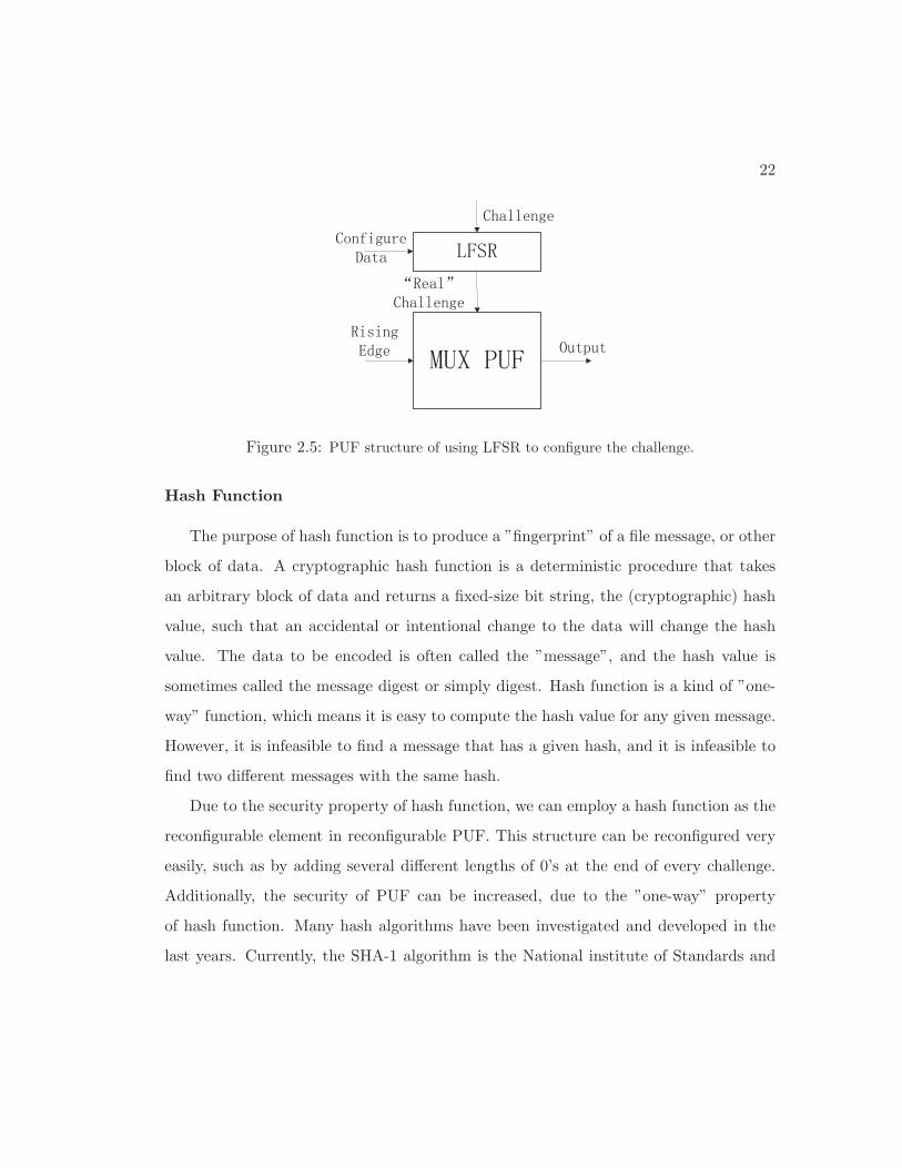
22
Figure 2.5: PUF structure of using LFSR to configure the challenge.
Hash Function
The purpose of hash function is to produce a ”fingerprint” of a file message, or other
block of data. A cryptographic hash function is a deterministic procedure that takes
an arbitrary block of data and returns a fixed-size bit string, the (cryptographic) hash
value, such that an accidental or intentional change to the data will change the hash
value. The data to be encoded is often called the ”message”, and the hash value is
sometimes called the message digest or simply digest. Hash function is a kind of ”one-
way” function, which means it is easy to compute the hash value for any given message.
However, it is infeasible to find a message that has a given hash, and it is infeasible to
find two different messages with the same hash.
Due to the security property of hash function, we can employ a hash function as the
reconfigurable element in reconfigurable PUF. This structure can be reconfigured very
easily, such as by adding several different lengths of 0’s at the end of every challenge.
Additionally, the security of PUF can be increased, due to the ”one-way” property
of hash function. Many hash algorithms have been investigated and developed in the
last years. Currently, the SHA-1 algorithm is the National institute of Standards and

23
technology (NIST) secure hash standard. Several hash function unit architectures have
been published in past years [21].
This structure has already been named as Control Physical Unclonable Function in
[22], which was described as using a strong PUF as a building block, but adding control
logic to prevent challenges from being applied freely to the PUF and hinder direct read
out of the response. Instead of performing a simple hash before the challenges are
applied to the PUF, we can consider adding another control logic, which would make
the CRPs updatable. We propose several reconfiguration methods:
(a) Adding different bit streams into the challenges, e.g., adding different numbers of
0’s at the end of the challenges.
(b) Reordering the challenge stream by certain rules.
(c) Reconfiguring the hash function, by using the reconfigurability of these reconfig-
urable Hash Function implementations.
Due to the property of hash function, it is extremely hard for adversary to model
the PUF, even after we configure it several times, as each output of the hash function
is unpredictable.
Output Recombination
Another idea is to add extra reconfigurable element to pre-process the output of
the arbiter before using it as an authentication key. One simple example is to use two
parallel MUX PUFs to update the CRPs, as shown in Figure 2.6. In this case, 4 paths
are selected by challenges through which the signal (rising edge) will propagate. Then
we can select two of the four paths using the configuration data and forward to the
arbiter to generate the response. We will have total 12 possible combinations if we
use a 2 level parallel structure. Therefore, we can reconfigurable this architecture 12
times. However, there will be very high correlation between some of these 12 different

24
possible combinations. For example, if we know that path 1 is faster than path 2, and
path 2 is faster than path 3, we can know definitely that path 1 will be faster than
path 3. Therefore, there should be some constraint for the reconfiguration, and the
total possible reconfigurations will decrease. Actually, there are N ! possible cases for
ordering N paths based on their arrival time. Therefore, log2(N !) independent bits can
be produced by N paths.
Figure 2.6: Two parallel MUX PUF structure.
However, there will be a problem by employing this structure, since the pre-processing
component after the last stage also has variations, which will affect the performance of
the PUF. To solve this problem, we can pre-process the data after the arbiters, as in
structure of Figure 2.7.
If we use N MUX-based PUF circuits, we will need 2N-1 arbiters, while we only
compare the neighbor paths. This is a concept borrowed from ring oscillator PUF
which could ensure there will be no correlation between the output bits of the arbiters,
as the comparison pairs are non-cyclic. If we want to achieve the bits’ entropy limit, we
need to choose the output comparison pairs adaptively, which would increase the design
complexity and fabrication area significantly.

25
Figure 2.7: MUX PUF structure of output recombination.

26
2.4.2 Reconfigurable Circuit Structure
Instead of only making the CRPs reconfigurable by processing the challenge and
response directly, we can reconfigure the main circuit to update the challenge-response
behavior. This kind of reconfigurable PUFs will have better performance from security
perspective, since after reconfiguration, it leads to a different PUF circuit, while the
previous method only changes the CRPs.
The most important thing in these structures is that, we must ensure the extra
circuit will not affect the PUF performance, or more generally, the extra circuit will
have identical effect on the delay of different paths statistically.
Reconfigure Feed-Forward PUF
It has been shown that the security of the MUX PUF in Figure 2.2 can be improved
by adding feed-forward arbiters to it [12]. However, in previous literature, how to choose
the feed-forward startpoints and endpoints, or how many paths (sometimes referred as
feed-forward loop in the literature [8]) are chosen for feed-forward purpose have not been
clearly presented. One constraint is trivial: the signal produced by the feed-forward
arbiter should arrive earlier than the two signals propagating through the MUX paths.
Therefore, we should ensure that the feed-forward path has at least 3-5 stages between
the input and output of the feed-forward arbiter. We denote the stages from the input
of a feed-forward arbiter to the output of the feed-forward arbiter as a feed-forward
loop. We consider the following three feed-forward structures:
(a) Feed-forward Overlap (FFO): This structure has at least one stage overlap between
two feed-forward paths.
(b) Feed-forward Cascade (FFC): In this structure, the endpoint of a feed-forward
path will be the starting stage of another feed-forward path.
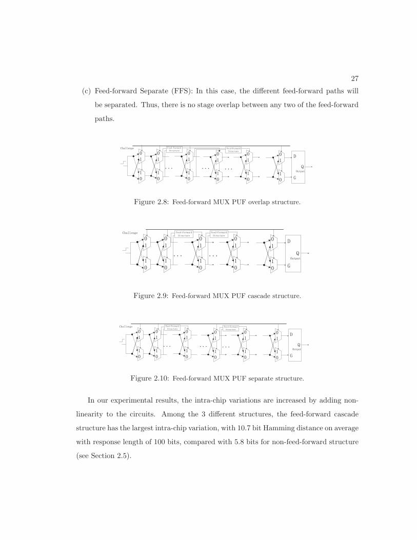
27
(c) Feed-forward Separate (FFS): In this case, the different feed-forward paths will
be separated. Thus, there is no stage overlap between any two of the feed-forward
paths.
Figure 2.8: Feed-forward MUX PUF overlap structure.
Figure 2.9: Feed-forward MUX PUF cascade structure.
Figure 2.10: Feed-forward MUX PUF separate structure.
In our experimental results, the intra-chip variations are increased by adding non-
linearity to the circuits. Among the 3 different structures, the feed-forward cascade
structure has the largest intra-chip variation, with 10.7 bit Hamming distance on average
with response length of 100 bits, compared with 5.8 bits for non-feed-forward structure
(see Section 2.5).

28
By utilizing this property, we propose the Reconfigurable Feed-forward MUX PUF
structure. A basic example that combines overlap and separate approaches is shown
in Figure 2.11. The structure can be configured among the 3 different structures ((a)
overlap, (b) cascade, (c) separate), which will make the PUF model more complex. By
configuring the PUF, the mathematical model for the PUF will be altered. This makes it
infeasible for attackers to break the PUF by only using one single uniform linear model.
The delay of MUXs connected after the feed-forward structure (normally just an arbiter)
may also affect the delay difference of the two paths. However, this time difference could
add into the total path delay difference both positively and negatively, depending on
the select signal. Therefore, the effect of these MUXs would be statistically equivalent
to the two paths of original MUX PUF, even if the delay of the added two MUXs vary
quite significantly. From above, we conclude that the MUX based PUF will be more
secure when feed-forward arbiter is reconfigurable.
Figure 2.11: Logic-reconfigurable feed-forward MUX PUF.
DeMUX and MUX PUF
The function of MUX is multiplexing; it selects one of many input signals and
forwards the selected signal into a single line. The DeMUX is a device that takes a single
input signal and distributes it over multiple output signals. Using DeMUX enables us
to select the direction of the propagating signal, and makes the PUF reconfigurable.

29
The select signal applied to the DeMUX can also be regarded as the challenge, which
would be similar to the structure of reconfigurable feed-forward PUF.
A basic reconfigurable structure is shown in Figure 2.12. Instead of propagating the
rising edge signal successively, we can choose to skip some stages by adding DeMUX
components, which could make the challenge-response behavior reconfigurable and hard
to predict. This structure will be harder for attackers to model than the silicon PUF
only based on MUX.
Figure 2.12: MUX and DeMUX PUF structure.
2.5 Experimental Results
All of our experiments are carried out using SPICE simulations on a 65-nm technolo-
gy process. We use Monte Carlo method to simulate the effect of process variations and
environmental variations. In our simulation, we set up the transistor parameters and
process variations based on a major industrial standard model. Each proposed structure
has been simulated over at least 20 Monte Carlo runs in SPICE. The simulated MUX
based Physically Unclonable Functions all have 100 stages. Accordingly, we need to
apply a 100-bit challenge to the PUF to produce a 1-bit response, and we apply 100
different challenges to generate the final 100-bit digital signature for each IC.
Measuring inter-chip variations: The inter-chip variations were determined by
comparing the digital signature of each IC to each other and calculate the Hamming
Distance between the two signatures. Since we had 20 chip instances, we had 20*19/2,
30
i.e., 190 possible digital signature comparisons. We use the maximum and the minimum
of these numbers as measures of the inter-chip variation.
Measuring intra-chip variations: The intra-chip variations were determined by
comparing the digital signal processing of the same IC under different environmental
conditions. In our case, we use temperature as the primary factor. We also simulated
the intra-chip variations under different voltages, from 1V to 1.2V . However, it is
shown that the intra-chip variations introduced by different temperatures from 0oC to
100oC were more significant compared to the intra-chip variations caused by voltage
variations. The digital signatures of the PUF at 0oC, 20oC, 40oC, 80oC, 100oC were
obtained; however, we only present the comparisons of Hamming Distance between 0oC
and 100oC, as those exhibit the largest variations. We simulated 10 different CRPs for
each IC, and simulated 20 different IC instances. Therefore we have 200 comparisons
in total. We provide the maximum and the average of the Hamming distances for the
intra-chip variations.
Simulation circuit structures: As presented in the previous section, we simulated
the digital signature for each proposed Physical Unclonable Function structure. We
add 10 feed-forward arbiters for each feed-forward PUF. For instance, the feed-forward
arbiters are from stage 1 to stage 11, from stage 11 to stage 21 ... from stage 91 to
stage 100 in a feed-forward cascade structure. The feed-forward arbiters are from stage
1 to stage 7, from stage 11 to stage 17 ... from stage 91 to stage 97 in feed-forward
overlap structure. In a feed-forward cascade structure, the feed-forward arbiters are
from stage 1 to stage 51, from stage 6 to stage 56 ... from stage 46 to stage 96.
For the reconfigurable feed-forward structure, we also add 10 such arbiters and MUX
structures into the original PUF circuit, which can switch among the 3 different feed-
forward structures. Moreover, we also simulated 10 DeMUX components in the MUX
and DeMUX PUF, the inputs and the outputs of the DeMUXs are from stage 3 to
stage 8, from stage 13 to stage 18 ... from stage 93 to stage 98. Finally, we simulated
20 parallel MUX PUFs for the output recombination structure. Therefore, we have 40

31
paths in total, and we derived the digital signature by comparing adjacent paths. In
other words, the delay of the first path was compared with that of the second path,
which is the same as a single PUF. The delay of the second path was compared with
that of the third path, and so on. Finally, the delay of the 39th path was compared
with that of the 40th path. Therefore, except for the first and the last paths, each path
was compared to two other paths.
Measuring reconfigurability: We randomly choose the configure data of the
different structures, and then fix the configure data when examining the inter-chip
variations and the intra-chip variations. However, when we add the reconfigurable
components into the circuits, the challenge-bit lengths are decreased; therefore, we
need to adjust the challenge bits when simulating these reconfigurable structures. To
test the reconfigurability, we simply fix the challenge bits, but change the configure
data to compare the digital signatures. All the simulations were carried out under the
environmental condition of 25oC and 1.1V .
Table 2.1 presents the inter-chip variations and intra-chip variations for different
MUX Physical Unclonable Function structures. First, it can be observed that the min-
imum inter-chip variation is larger than the maximum intra-chip variation for all of the
simulated structures. Thus, we can conclude that the variations caused by the random-
ness in manufacturing process are more significant than the variations under different
environmental conditions. Therefore, these PUFs can be used as reliable secret keys
with some error correcting techniques. Second, it can also be observed that by adding
feed-forward arbiters into the MUX PUF circuit, the inter-chip variations and intra-chip
variations are both increased, since the noise can have influence on the select signals
of some intermediate stages. By comparing the inter-chip variations and the intra-chip
variations, we conclude the feed-forward separate structure is the most reliable struc-
ture while the feed-forward cascade is the least reliable one among the 3 feed-forward
structures. The reconfigurable feed-forward structure has very close performance to
the 3 types of feed-forward structures, since its functionality is switching among the 3.

32
Moreover, the reconfigurable DeMUX and MUX PUF has similar inter-chip variation as
the non-feed-forward structure, but the intra-chip variation is increased, as the number
of stages is reduced by some configurations. Therefore, the reliability of this structure
is decreased.
Table 2.1: Simulation Results: VariationsInter-chip Variation Intra-chip Variation
Structures Max Min Max AvgNon-feed-forward 59 22 13 5.8
Feed-forward Overlap 66 27 15 8.7Feed-forward Cascade 64 25 20 10.7Feed-forward Separate 65 26 17 9.9
Reconfigurable Feed-forward 65 25 19 10.3MUX and DeMUX 57 23 16 7.1
Table 2.2 shows the reconfigurability of each reconfigurable structure. It can be seen
that the output recombination structure has the best reconfigurability, that is, by fixing
the challenge bits and only changing the configure data, the digital signature would
vary most significantly. In our simulation result, the average variation is 38.7 bits. The
MUX and DeMUX PUF exhibits the least reconfigurability; that is because the func-
tion of the DeMUX is only to determine whether to skip some stages or not. When the
process variations of other stages are relatively large, the difference of digital signatures
with two different configure data may only vary a little bit. For output recombination
structure, it is similar to comparing different paths with different configurations, so its
performance is close to the inter-chip variation of the non-feed-forward MUX PUF. It
also can be observed that although the challenge hash structure and the challenge LFSR
structure both pre-process the challenge before it is applied to the circuit, their recon-
figurability still have some difference. As the challenge LFSR appears to have better
reconfigurability, we can conclude that the number generated by the LFSR in our case
may have better randomness than that of the Hash Function. Finally, the proposed
reconfigurable feed-forward MUX PUF has the average Hamming distance 32.4 bits by

33
different configurations, which will be sufficient to be used as a secure and reliable secret
key storage method, considering its complex and nonlinear functionality.
Table 2.2: Simulation Results: ReconfigurabilityVariation
Structures Max Avg MinChallenge LFSR 44 34.6 28Challenge Hash 42 28.3 19
Output recombination 57 38.9 25Reconfigurable Feed-forward 47 32.4 22
MUX and DeMUX 33 24.7 13
Overall, all the proposed reconfigurable structures have considerable reconfigurabili-
ty, and can be used for reliable authentication and identification within certain error tol-
erance, as the minimum of the inter-chip variations would be larger than the maximum
intra-chip variation. The output recombination structure has the best reconfigurable
ability; however, we consider the reconfigurable feed-forward MUX PUF to have the
best performance due to its security, as it is extremely hard to be modeled by certain
linear modeling methods.
2.6 Conclusion
We have presented several reconfigurable silicon MUX Physical Unclonable Function-
s based on two major approaches and demonstrated their effectiveness by experimental
results via inter-chip variation and intra-chip variation. We also have discussed the
reliability perspective of PUFs and proposed several methods to increase the security.

Chapter 3
Statistical Analysis of
MUX-based Physical Unclonable
Functions
3.1 Introduction
Physical Unclonable Functions (PUFs) [2, 22, 4] are novel security primitives which
store secret keys in physical objects by exploiting the uncontrollable randomness due
to manufacturing process variations. PUFs generate signatures based on the unique
intrinsic uncontrollable physical features, which can then be used for hardware authen-
tication or the generation of secret keys. Contrary to standard digital systems, PUFs
extract secrets from complex properties of a physical material rather than storing them
in a non-volatile memory. It is nearly impossible to predict, clone or duplicate PUFs.
Furthermore, an adversary cannot easily mount an attack to counterfeit the secret infor-
mation without changing the physical randomness. Based on these advantages, PUFs
can efficiently and reliably generate volatile secret keys for cryptographic operations
and enable lightweight and cost-effective authentication of ICs.
34

35
The performance of a PUF depends on both process variations and environmental
conditions. Designing a PUF that is close to truly random in nature and that can
operate reliably over a wide range of operating conditions is still a challenge. Some
metrics have been introduced to evaluate the performances of PUFs by analyzing the
outputs of PUF instances. These considered metrics include reliability, uniqueness, and
randomness. PUF reliability captures how efficient a PUF is in reproducing the response
bits of an IC chip. When the same challenge is applied repetitively to a MUX-based
PUF, the responses are expected to be identical. Uniqueness represents the ability of
a PUF to uniquely distinguish a particular chip among a group of chips of the same
type. When the same challenge sets are applied to different PUFs, the output responses
are expected to be different. Ideally, the Hamming distances between the responses
of different PUFs should be 50%. Randomness indicates the unbiasedness of the PUF
response. However, these metrics need to be characterized over a large population
of chips to validate the effectiveness of PUFs. This can involve a long and costly chip
manufacturing process followed by many measurements after the circuits are fabricated.
Furthermore, since the manufacturing process variation and the environmental variation
are uncontrollable, it is hard to get a very accurate estimation of the performance during
the design stage. Note that security is another performance metric of PUFs, which is
not addressed in this chapter. A PUF is more secure, if an adversary finds it harder to
break in.
Knowledge about the circuit-level behavior such as process variation pattern, varia-
tion of circuit parameters (e.g., delay, threshold voltage) over changing operating condi-
tions could help designers to predict the performance comparisons among different PUF
designs. Conducting the performance comparison among detailed PUF designs before
fabrication would guarantee robust on-chip PUF performance. Monte-Carlo simulations
of netlists that take process and environment variations into account can be used for
this purpose. These simulations can provide approximate results, which can be used as

36
indicators of the true performances of different PUFs. An alternate approach to evalu-
ate the performance of the PUFs is by modeling the physical components of PUFs in a
statistical manner. A number of such efforts have been developed in the literature. Sta-
tistical analysis on Coating PUF has been presented in [23]. In [24], entropy analysis of
Optical PUF has been discussed. The statistical models of Ring Oscillator PUF [25, 26]
and MUX PUFs [27, 28, 29] have also been studied in the literature. Additionally, the
work in [30] relates the statistical analysis of PUFs to circuit-level optimization and
architecture-level optimization, which leads to interesting results that could improve
the design and implementation of reliable and efficient PUFs.
The objective of this chapter is to theoretically compare the performances of different
MUX-based PUFs to predict the relative advantages of various MUX-based PUF de-
signs. In previous works, such as the efforts in [27, 28, 29], only the statistical modeling
with respect to the input-output mappings of PUF structures was presented. However,
theoretical performances of PUFs based on these models were not studied. Additionally,
there seems little consensus about which PUF is more suitable for a specific application
or a particular device in the existing literature. The work presented in this chapter
differs from existing efforts in several respects. First, to the best of our knowledge, this
work, for the first time, presents a systematic statistical analysis of the performances of
various MUX-based PUFs. These include the original MUX PUF, feed-forward MUX
PUFs, and multiplexer-demultiplexer (MUX/DeMUX) PUF. Moreover, the focus of
our work is on the comparison of performance of various MUX PUFs, which could help
the designer to select an appropriate PUF during the design stage. Finally, instead of
only modeling the structures of various MUX-based PUFs, statistical analysis is per-
formed to provide a deeper insight into the nature of these PUFs. Equations about the
PUF performances are derived; these equations allow the designer to estimate the PUF
performance metrics theoretically. In addition, we also introduce a class of modified
feed-forward MUX PUFs obtained by modifying the standard feed-forward path. These

37
structures are also analyzed statistically. It is shown that the modified feed-forward
MUX PUFs have less intra-chip variations than standard feed-forward MUX PUFs.
3.2 Modified Feed-Forward MUX PUFs
3.2.1 Modified Feed-Forward Path
In this section, we propose a novel modified feed-forward MUX PUF structure shown
in Figure 3.1, which is motivated by our statistical analysis results. In this structure,
the output of a feed-forward arbiter from an intermediate stage is input as the challenge
bit to two consecutive late MUX stages. By employing this modified feed-forward path,
the reliability of the feed-forward PUF structure can be improved, while the same level
of security will be retained. This structure is analyzed statistically in this chapter.
0
0 0
1 1
0
1 1
0
0
1
1
. . .
FF Arbiter0
0
1
1
ArbiterOutput
. . .
0
0
1
1
Figure 3.1: Modified feed-forward MUX PUF structure.
The complexity of the modified feed-forward MUX PUFs can be further improved
by using several modified feed-forward paths in a PUF circuit. Note that if we want
to maintain the length of challenge bits as N , we need to increase the number of MUX
stages to N + 2M for the modified feed-forward structure, compared to N +M of the
standard feed-forward PUF, where M represents the number of feed-forward paths.
Additionally, the design overhead will also include M arbiters for both the standard
feed-forward MUX PUF and the modified feed-forward MUX PUF.

38
3.2.2 Different Types of Modified Feed-Forward MUX PUFs
Similar to the three types of the standard feed-forward MUX PUFs as discussed
in Chapter 2, the modified feed-forward MUX PUFs can also be classified as Modified
Feed-Forward Overlap (MFFO), Modified Feed-Forward Cascade (MFFC), and Modified
Feed-Forward Separate (MFFS) as shown in Figure 3.2, Figure 3.3, and Figure 3.4,
respectively.
0
0 0
1 1
0
1 1
0
0
1
1
. . .
Challenge FF Arbiter0
0
1
1
ArbiterOutput
. . .
0
0
1
1
FF Arbiter0
0
1
1
. . . . . .
0
0
1
1
0
0
1
1
Figure 3.2: Modified feed-forward MUX PUF overlap structure.
0
0 0
1 1
0
1 1
0
0
1
1
. . .
Challenge FF Arbiter0
0
1
1
ArbiterOutput
. . .
0
0
1
1
FF Arbiter
. . .
0
0
1
1
0
0
1
1
Figure 3.3: Modified feed-forward MUX PUF cascade structure.
0
0 0
1 1
0
1 1
0
0
1
1
. . .
Challenge FF Arbiter0
0
1
1
ArbiterOutput
. . .
0
0
1
1
FF Arbiter0
0
1
1
. . . . . .
0
0
1
1
0
0
1
1
Figure 3.4: Modified feed-forward MUX PUF separate structure.
These three different structures also have different inter-chip and intra-chip behav-
iors, which are analyzed in Section 3.5. Additionally, the modified feed-forward paths
can also be used in the Logic-Reconfigurable Feed-forward MUX PUF as presented in
Section 2.4.2 to improve the reliability while retaining the high security.

39
3.3 Definition of PUF Performance
As discussed in Section 3.1, Monte-Carlo simulation can be used to provide per-
formance indicators for different PUF designs. For example, by simulating the three
feed-forward MUX PUF structures with the same parameter variations and environmen-
tal conditions, we were able to conclude in [31, 32] that the FFO structure is the most
reliable among the three feed-forward structures. We focus on analyzing the quantita-
tive performance of various MUX-based PUFs through statistical modeling of the delay
variations and environmental variations. Performance indicators ranging from 0 to 1
with 1 representing the best performance are generated through a theoretical analysis.
The notations used in this chapter are listed in Table 3.1.
Table 3.1: Notation Used in the ChapterNotation Explanation
N Number of MUX stages in a PUF instanceM Number of feed-forward pathsL Length of a responseCi Challenge bit of the i-th MUX stageDt
i Delay of the top element of the i-th MUX stageDb
i Delay of the bottom element of the i-th MUX stageΔi Delay difference between top and bottom elements of the i-th MUX stage
ΔArb Skew effect of the arbiterrN Delay difference of N stagesR Response
In this section, we introduce three PUF metrics to quantify the performance of
MUX-based PUFs. The relative performance behaviors of the PUF structures are the
main concern of this chapter rather than the absolute value of each indicator.
3.3.1 Reliability
Intra-chip variation is a measure of the reliability of PUF, which is determined
by comparing the digital signatures of the PUF to the same challenge under different
environmental conditions.
40
Let Pintra represent the probability that a certain bit of a response will flip when
applying a randomly selected challenge multiple times. All the bits of a PUF response
have the same value of Pintra, since each bit is generated independently by a same PUF
instance (i.e., the effects of manufacturing process variation and environmental variation
for all the bits are the same). As a result, Pintra can be used to represent the intra-chip
variation for the entire L-bit response. In particular, the average Hamming distance
(HD) between the responses is used to measure the intra-chip variations of MUX-based
PUFs. The Pintra and the averaged HD are described by:
E(HDintra) = Pintra = E
(1
m
m∑i=1
HD(R,R′)
L× 100%
), (3.1)
wherem is the number of HD comparisons, and R and R′ represent two measurements of
the PUF response under different conditions. The expected value of HDintra is equal to
Pintra. If the responses are sampled sufficient number of times, the averaged intra-chip
variation would be close to the value of Pintra.
As smaller intra-chip variation means better reliability, the reliability indicator is
defined as
Reliability = 1− Pintra. (3.2)
3.3.2 Uniqueness
Inter-chip variation is a measure of the uniqueness of PUF, which is determined
by comparing the digital signature of a PUF to that of another. Similarly, we can also
define Pinter as the probability that the bits generated by the same challenge for different
PUF instances are different. Since uniqueness is a measure of inter-chip performance,
all possible chip-combinations should be considered. Therefore, the average inter-chip

41
HD of K PUFs can be described as:
E(HDinter) = Pinter
=E
⎛⎝ 2
(K − 1)K
K−1∑i=1
K∑j=i+1
HD(R(i), R(j))
L× 100%
⎞⎠ . (3.3)
It can also be seen that Pinter represents the expected value of the inter-chip variation.
Since Pinter = 50% represents the best uniqueness for a PUF, the uniqueness indicator
can be defined by:
Uniqueness = 1− |2Pinter − 1|. (3.4)
3.3.3 Randomness
AMUX-based PUF is expected ideally to produce unbiased 0’s and 1’s. Randomness
represents the ability of the PUF to output 0 and 1 response with equal probability.
One measurement of the randomness can be expressed as:
Randomness = 1− |2P (R = 1)− 1|. (3.5)
Therefore, a randomness of 1 indicates unbiased PUF responses.
3.4 Performance Analysis of the Original MUX PUF
3.4.1 Physical Component Modeling of MUX-based PUFs
As shown in Figure 2.1, a MUX PUF consists of a sequence of MUXs and an arbiter.
The rising edge signal excites the two paths at the first stage simultaneously. The actual
propagated paths are determined by the external challenge bits. After the last stage, the
arbiter will generate the output bit by comparing the arrival time of the two paths at
its input. It has become standard to model the MUX PUF via an additive linear delay
model [27, 28]. According to the efforts in the field of statistical static timing analysis
(SSTA) [11], the manufacturing process variations for the parameters of transistors can

42
be modeled as Gaussian distributions. As a result, the variations of the delays will also
be approximately Gaussian.
Process variations are classified as follows: inter-die variations are the variations
from die to die, while intra-die variations correspond to variability within a single chip.
Inter-die variations affect all devices on the same chip similarly, while intra-die variations
affect different devices differently on the same chip. A very widely used model for delay
spatial correlation is the ”grid model” [11], which assumes perfect correlations among
the devices in the same grid, high correlations among those in nearby grids, and low or
zero correlations in faraway grids, since devices close to each other are more likely to
have similar characteristics than those placed far away.
Additionally, experimental results in [10] have already shown that the inter-chip
variation for MUX PUF across the wafers is similar to that within a single wafer, as
the output of the arbiter in silicon MUX PUF is only based on the difference of two
selected paths. Therefore, these die-to-die, wafer-to-wafer, and lot-to-lot manufacturing
variations will have minimum effect on the output response.
Based on the facts discussed above, for simplicity, we can model the delay of each sin-
gle MUX as an independent identically distributed (i.i.d.) random variable Di, modeled
by a Gaussian random variable N(μ, σ2), where μ represents the mean and σ represents
the standard deviation of the delay of each MUX. Therefore, the total delay of the N
stages is modeled by N(Nμ,Nσ2). The delay difference between top and bottom MUXs
of the i-th stage will also follow a Gaussian distribution, and can be expressed as:
Δi = Dti −Db
i ∼ N(0, 2σ2). (3.6)
For the original MUX PUF, the response is dependent on the delay difference of the
two selected paths. The sign of the delay difference of each stage is determined by the
external challenge bits. Consequently, the delay difference after the last stage can be
modeled as
rN =
N∑i=1
(−1)C′iΔi, (3.7)

43
where C ′i = ⊕N
j=i+1Cj and C ′N = 0. The output bit is generated by
R = sign(rN ) =
⎧⎪⎨⎪⎩1, rN ≥ 0
0, rN < 0
. (3.8)
It can be seen that the original MUX PUF forms an additive linear model.
In a real PUF circuit, the arbiter would not be ideal. The skew effect of the arbiters
also affects the performance of MUX-based PUFs by reducing the uniqueness, producing
a biased response, and even degrading the security. If we assume that the threshold of
the arbiter is ΔArb, the response is given by
R = sign(rN ) =
⎧⎪⎨⎪⎩1, rN ≥ ΔArb
0, rN < ΔArb
, (3.9)
since the arbiter is preset to 0 and requires a setup time constraint to switch to 1.
3.4.2 Probability Distribution of Output Delay Difference
Figure 3.5 shows a scatter plot of output samples from the simulations of 100-stage
original MUX PUFs. Note that there are overlaps between the regions of output 1’s
and output 0’s, which makes it difficult to estimate ΔArb accurately. This could be
because the measured delay differences (measured for each path at the 50% point in the
transition) and the actual delay differences that the arbiter operates at are different.
Since the delay difference can be modeled by N(0, 2Nσ2), we fit a Gaussian distribution
to the delay differences, as shown in Figure 3.6. The standard deviation√2Nσ2 of the
generated Gaussian distribution is 5.2936 × 10⁻¹¹. It can be seen that the skew effect
of the arbiter leads to biased outputs with 32.8% 1’s and 67.2% 0’s.
Moreover, the average of the total delay of one path is 1.2667 × 10⁻⁸s in our sim-
ulation results. Therefore, the percent of delay deviation of 100 stages is about 0.4%
(i.e.,5.2936×10−11
1.2667×10⁻⁸ ), which conforms with other published results of 65nm technology (e.g.,
[9]).

44
Delay Differences (s) Delay Difference (s)
Out
put
Figure 3.5: Scatter plot of outputs.
32.8%output = 132.8%
output = 067.2%
Delay Difference (s)
Gau
ssia
n Fi
t Pro
b
Figure 3.6: Gaussian fit curve of delay difference distribution.

45
3.4.3 Effect of Number of Stages
The probability that the output is equal to 1 can be derived as:
P (R = 1) = P (
N∑i=1
(−1)C′iΔi ≥ ΔArb)
=
∫ ∞
ΔArb
1√2πN2σ2
exp(−x2
2N2σ2)dx
=1
2− 1
2erf(
ΔArb√2N2σ2
). (3.10)
It can be seen that P (R = 1) is also dependent on the number of stages in a MUX
PUF. If we only consider the number of stages N as a variable, the above equation can
be rewritten as
P (R = 1) =1
2− 1
2erf(
K√N
), (3.11)
where K is a constant and is equal to ΔArb√4σ2
. Thus, although the value of ΔArb is unclear,
we can still estimate the K based on the experimental results:
K =√N × erfinv(1− 2P (R = 1)). (3.12)
In our simulations, the 50-stage MUX PUF structure is only able to generate 1’s
with probability 25.6%, which is very close to the value of P (R = 1) = 26.4% that is
calculated theoretically from Equation (3.11).
3.4.4 Statistical Properties of the Original MUX PUF
Reliability
In order to analyze the reliability, we need to consider the effect of environmental
noise. As a usual practice, we assume that the noise ni of the i-th stage follows a
zero-mean Gaussian distribution with variance σ2n. Then, Pintra can be described as:
Pintra =P [sign(
N∑i=1
(−1)C′iΔi +
N∑i=1
ni) �= sign(
N∑i=1
(−1)C′iΔi +
N∑i=1
n′i)], (3.13)

46
where ni and n′i represent the noise under different environmental conditions. As each
individual stage follows the zero-mean i.i.d. Gaussian distribution, then the intra-chip
variation probability is equivalent to a single stage intra-chip variation probability:
Pintra = P [sign(si + ni) �= sign(si + n′i)] (3.14)
where si = (−1)Ci(Dti −Db
i ) has a variance that is equal to 2σ2.
As manufacturing process variation and environmental noise of the delay difference
both follow zero-mean Gaussian distribution, their probability density functions (PDF)
are given by:
fs(s) =1√2πσ2
s
exp(− s2
2σ2s
), fn(n) =1√2πσ2
n
exp(− n2
2σ2n
). (3.15)
Note that σ2s = 2σ2 in Equation (3.6). Pintra of an original MUX PUF can be calculated
as
Pintra =P [sign(si + ni) �= sign(si + n′i)]
=4
∫ ∞
0
1√2πσ2
s
exp(− s2
2σ2s
)
∫ −s
−∞1√2πσ2
n
exp(− n2
2σ2n
)dn
∫ ∞
−s
1√2πσ2
n
exp(− n′2
2σ2n
)dn′ds
=4
∫ ∞
0
1√2πσ2
s
exp(− s2
2σ2s
)(1
4− 1
4erf2(
s√2σ2
n
))ds
=
∫ ∞
0
1√2πσ2
s
exp(− s2
2σ2s
)ds−∫ ∞
0
1√2πσ2
s
exp(− s2
2σ2s
)erf2(s√2σ2
n
)ds
=1
2− 1
πarctan(
√σ4s
2σ2sσ
2n + σ4
n
), (3.16)
where the first of the two integrals in the fourth line represents integrating just a Gaus-
sian over half of the space, and the second is a known definite integral [33].
It can be seen that by increasing the ratio of manufacturing process variation to
environmental variation, the intra-chip variation can be reduced to close to 0.
If we consider the Pintra of the PUF response with a given challenge, the conditional
probability can be derived as
P [sign(si + ni) �= sign(si + n′i)|si] =
1
2− 1
2erf2(
|si|√2σ2
n
). (3.17)

47
The reliability for a certain challenge-response pair is greatly dependent on the manu-
facturing process variation between the two generated paths. If a challenge selects two
paths with rN ≈ 0, the variation is large, since the above equation achieves maximum
at si = 0. Otherwise, if |rN | is relatively large, the manufacturing process variation
would be the primary factor to determine the output and the noise would hardly flip
the response.
However, if we take the skew effect of non-ideal arbiters into consideration, the
intra-chip variation behaviors would also be dependent on the number of stages and the
performance of the arbiter. The response then can be described as sign(∑N
i=1(si+ni)−ΔArb). Therefore, Pintra is given by
P [sign(N∑i=1
(si + ni)−ΔArb) �= sign(
N∑i=1
(si + n′i)−ΔArb)]. (3.18)
If we combine∑N
i=1 si and ΔArb as a variable X ∼ (ΔArb, Nσ2s), Pintra can be
expressed as P [sign(x+n) �= sign(x+n′)], where x ∼ N(−ΔArb√N
, σ2s) and n ∼ N(0, σ2
n).
Therefore, according to Equation (3.18), the intra-chip variation probability decreases
with the increase of ΔArb. Intuitively we would expect this as when ΔArb is relatively
large and the number of stages is small,∑N
i=1(si + ni) will have a high probability of
unaltered sign() value. However, if the number of stages is relatively large that ΔArb√N
approaches to 0, Pintra will be reduced to Equation (3.16).

48
A closed-from expression for Pintra (i.e., Equation (3.18)) does not exist, but we can
derive the expression by using a first-order approximation of the exponential function:
P [sign(
N∑i=1
(si + ni)−ΔArb) �= sign(
N∑i=1
(si + n′i)−ΔArb)]
=2
∫ ∞
−∞1√2πσ2
s
exp(− s2
2σ2s
)(1
4− 1
4erf2(
|s− Δarb√N|√
2σ2n
))ds
=2
∫ ∞
−∞1√2πσ2
s
exp(−(x+ Δarb√
N)2
2σ2s
)(1
4− 1
4erf2(
|x|√2σ2
n
))dx
≈2
∫ ∞
−∞1√2πσ2
s
exp(− x2
2σ2s
)(1− ΔArb
σ2s
√N
x)(1
4− 1
4erf2(
|x|√2σ2
n
))dx
=1
2− 1
πarctan(
√σ4s
2σ2sσ
2n + σ4
n
)− 4ΔArb
σ2s
√N
∫ ∞
0
x√2πσ2
s
exp(− x2
2σ2s
)(1
4− 1
4erf2(
x√2σ2
n
))dx
=1
2− 1
πarctan(
√σ4s
2σ2sσ
2n + σ4
n
)− ΔArb√2πNσ2
s
(1− 2
π
√σ2s
σ2s + σ2
n
arctan(
√σ2s
σ2s + σ2
n
)
)
(3.19)
It can be seen that Pintra increases with the number of stages, since
2
π
√σ2s
σ2s + σ2
n
arctan(
√σ2s
σ2s + σ2
n
)) < 1. (3.20)
Additionally, the term of√
σ2s
σ2s+σ2
nis close to 1, while the ratio of σs
σnis relatively large.
As a result,(1− 2
π
√σ2s
σ2s+σ2
narctan(
√σ2s
σ2s+σ2
n))will be close to 0. Therefore, in this case,
the number of the stages only has a minor influence on the intra-chip variation of the
original MUX PUF.
Conclusion 1: The reliability indicator of an original MUX PUF is
Reliability = 1− Pintra
=1
2+
1
πarctan(
√σ4s
2σ2sσ
2n + σ4
n
) +ΔArb√2πNσ2
s
(1− 2
π
√σ2s
σ2s + σ2
n
arctan(
√σ2s
σ2s + σ2
n
)
)
(3.21)

49
where σs is the standard deviation of manufacturing process variation for a single stage,
σn is the standard deviation of environmental noise, ΔArb is the skew effect of the ar-
biter, and N is the number of stages in an original MUX PUF. �
Uniqueness
In order to compute inter-chip variation based on the same mathematical model,
we need to compare the responses of different PUFs. The Gaussian fit curve for the
inter-chip variations of the 100-stage MUX PUF is shown in Figure 3.7. The average of
the inter-chip variation is 43.2%.
Gau
ssia
n Fi
t Pro
b
Inter-Chip Variation (%)
Figure 3.7: Gaussian fit curve of inter-chip variation distribution.
Theoretically, if the PUFs are uncorrelated, the expected inter-chip variation of the
original MUX PUF is simply given by
Pinter = 2P (R = 1)(1− P (R = 1))
=1
2− 1
2erf2(
K√N
), (3.22)

50
where K = ΔArb√4σ2
= ΔArb√2σ2
s
. Therefore, the value of uniqueness indicator can be expressed
as
Uniqueness =1− |2Pinter − 1| = 4P (R = 1)(1− P (R = 1))
=1− erf2(ΔArb√2Nσ2
s
). (3.23)
According to the value of P (R = 1), we could expect the average of the inter-
chip variation to be 2 × 0.328 × (1 − 0.328) = 44%, which is also consistent with our
experimental results.
Randomness
Similarly, according to Equation (3.10) in Section 3.4.3, the randomness of an orig-
inal MUX PUF is
Randomness = 1− |2P (R = 1)− 1| = 1− erf(ΔArb√2Nσ2
s
). (3.24)
3.4.5 Design Example
The above equations are useful for designing a PUF that could meet the specific
application requirement. Consider the scenario that the PUF designer has fabricated
a PUF and tested its performance. However, the designer found the performance of
the current PUF cannot satisfy the application requirement. Instead of fabricating a
large number of different PUF designs, the designer could utilize the statistical analysis
results to predict the performances of other PUF designs theoretically, since some of
the parameters can be calculated from the results of the current PUF. For example,
if we fabricate a 100-stage original MUX PUF which has the performance similar to
our experimental results, we can calculate the value of K by Equation (3.12) based on
the performance of the 100-stage MUX PUF. We can then substitute different values
of N to predict the performances of the original MUX PUFs for different numbers of
stages. For the intra-chip variation, we can obtain the relations among σs, σn, and ΔArb
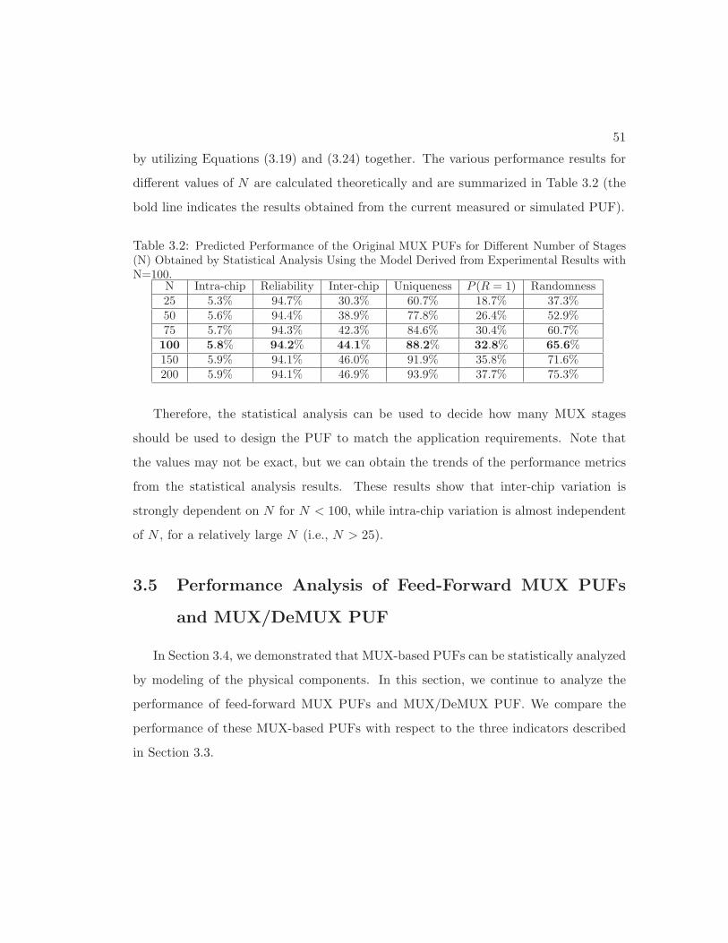
51
by utilizing Equations (3.19) and (3.24) together. The various performance results for
different values of N are calculated theoretically and are summarized in Table 3.2 (the
bold line indicates the results obtained from the current measured or simulated PUF).
Table 3.2: Predicted Performance of the Original MUX PUFs for Different Number of Stages(N) Obtained by Statistical Analysis Using the Model Derived from Experimental Results withN=100.
N Intra-chip Reliability Inter-chip Uniqueness P (R = 1) Randomness25 5.3% 94.7% 30.3% 60.7% 18.7% 37.3%50 5.6% 94.4% 38.9% 77.8% 26.4% 52.9%75 5.7% 94.3% 42.3% 84.6% 30.4% 60.7%100 5.8% 94.2% 44.1% 88.2% 32.8% 65.6%150 5.9% 94.1% 46.0% 91.9% 35.8% 71.6%200 5.9% 94.1% 46.9% 93.9% 37.7% 75.3%
Therefore, the statistical analysis can be used to decide how many MUX stages
should be used to design the PUF to match the application requirements. Note that
the values may not be exact, but we can obtain the trends of the performance metrics
from the statistical analysis results. These results show that inter-chip variation is
strongly dependent on N for N < 100, while intra-chip variation is almost independent
of N , for a relatively large N (i.e., N > 25).
3.5 Performance Analysis of Feed-Forward MUX PUFs
and MUX/DeMUX PUF
In Section 3.4, we demonstrated that MUX-based PUFs can be statistically analyzed
by modeling of the physical components. In this section, we continue to analyze the
performance of feed-forward MUX PUFs and MUX/DeMUX PUF. We compare the
performance of these MUX-based PUFs with respect to the three indicators described
in Section 3.3.

52
3.5.1 Statistical Properties of Feed-Forward MUX PUF
Reliability
As shown in Figure 2.2, some of the challenge bits of a feed-forward MUX PUF will
be the intermediate stage arbiter outputs instead of the external bits in a feed-forward
MUX PUF. For instance, if there is only one feed-forward path in a MUX PUF, which
is from the a-th stage to the b-th stage, the time difference of the b-th stage could be
expressed as:
Δb = (−1)sign(ra)(Dtb −Db
b). (3.25)
It can be expected intuitively that the intra-chip variation will be greatly dependen-
t on the location of the ending stage of the feed-forward path. If the challenge of
the last stage flips, the output bit will be sign(−∑N−1i=1 (−1)C
′iΔi + ΔN ) compared to
sign(∑N−1
i=1 (−1)C′iΔi +ΔN ) while there is no error. We can also illustrate this charac-
teristic of the feed-forward PUF mathematically. As an example, if the challenge of the
k-th stage flips in an N -stage structure, the probability that the output bit will change,
Pe, is given by (without considering noise):
Pe =P [sign(
k−1∑i=1
(−1)C′iΔi +
N∑i=k
(−1)C′iΔi) �= sign(−
k−1∑i=1
(−1)C′iΔi +
N∑i=k
(−1)C′iΔi)]
=2
∫ ∞
0
1√2π(N − k + 1)σ2
s
exp(− s2
2(N − k + 1)σ2s
)
(1−∫ s
−s
1√2π(k − 1)σ2
s
exp(− w2
2(k − 1)σ2s
))dwds
=2
∫ ∞
0
1√2π(N − k + 1)σ2
s
exp(− s2
2(N − k + 1)σ2s
)(1− erf(s√
2π(k − 1)σ2s
))ds
=1− 2
πarctan(
√N − k + 1
k − 1)
=2
πarctan(
√k − 1
N − k + 1) (3.26)
where the second integral in the third line is also a known definite integral in [33].

53
It can be seen that the probability Pe increases with k. Obviously, the problem for
this structure is that if the ending stage of a feed-forward path is close to the last stage,
the reliability of the PUF will be degraded significantly. If k = N , i.e., the ending stage
of the feed-forward path is the last stage, Pe will be 2πarctan(
√N − 1), which is close
to 1.
Therefore, Pintra of this feed-forward MUX PUF with single feed-forward path can
be described as
(1− P1)P1 + P12
πarctan(
√k − 1
N − k + 1), (3.27)
where P1 is equal to Pintra of the original MUX PUF. Note that, for simplicity, the
following analysis on reliability will focus on the case without considering the skew
effect of arbiters (i.e., P1 represents Equation (3.16) instead of Equation (3.19)), since
the number of stages and the skew effect do not have a significant impact on intra-chip
variation, as described in Section 3.4. Additionally, there could be a number of feed-
forward paths in one PUF design. In these PUFs, if the ending stage of a feed-forward
path is close to the last stage, the reliability of the PUF will be degraded significantly.
3.5.2 Statistical Properties of Modified Feed-Forward MUX PUF
Motivated by this analysis, we propose the modified feed-forward MUX PUF struc-
ture shown in Figure 3.1, which is presented in Section 3.2. The modified feed-forward
path mitigates the effect of the locations of feed-forward paths. In this structure, the
modified feed-forward path only affects the delay difference of one stage. For example,
if the two consecutive ending stages of a feed-forward path are the k-th and (k + 1)-th
stages respectively, we can derive C ′ for the modified feed-forward MUX PUF as follows:
C ′k−1 = ⊕N
j=k+2Cj ⊕ Ck ⊕ Ck+1, (3.28)
C ′k = ⊕N
j=k+2Cj ⊕ Ck+1, (3.29)

54
C ′k+1 = ⊕N
j=k+2Cj . (3.30)
Since Ck = Ck+1 in this structure, the modified feed-forward path will only affect the
value of C ′k.
As a result, by employing this modified feed-forward path, only one stage will be
affected by each feed-forward arbiter. Thus, this structure will have lower intra-chip
variation, compared to the standard feed-forward MUX PUF. However, the nonlinearity
of mathematical models for the modified feed-forward MUX PUF and the standard feed-
forward MUX PUF are similar, except the challenge mapping C ′i. Therefore, we can
conclude that one benefit of using the proposed modified feed-forward path is that the
reliability of the feed-forward MUX PUF can be improved. Furthermore, the modified
feed-forward path can lead to higher security, as the degree of nonlinearity can be
increased without significant increase of intra-chip variation.
The designer can predict the performances of different implementations of the feed-
forward MUX PUFs based on above statistical analysis results. For example, we consider
the 100-stage feed-forward MUX PUFs with one feed-forward path (assuming that the
feed-forward path starts from the output of the 20th stage, and the ends at the k-th
stage). If error occurs in the feed-forward path, the probabilities that the output bit will
change Pe and the intra-chip variation probabilities, Pintra, are summarized in Table 3.3
(P1 is equal to 5.8% in our experimental results). Note that the probabilities of errors
in the feed-forward paths are the same for all the feed-forward MUX PUFs with single
feed-forward path, since there is no feed-forward path in previous stages.
Table 3.3: Performances of Different Feed-Forward MUX PUFsStandard Feed-Forward MUX PUF Modified Feed-Forward MUX PUF
k 50 70 90 50 70 90Pe 49.4% 62.4% 78.5% 6.4% 6.4% 6.4%
Pintra 8.33% 9.09% 10.02% 5.83% 5.83% 5.83%

55
It can be seen that the modified feed-forward path can reduce the intra-chip varia-
tion of the feed-forward MUX PUF. Compared to the original MUX PUF, the intra-chip
variation of the modified feed-forward MUX PUF with single feed-forward path is only
increased very slightly. Based on Table 3.3, it can also be concluded that if the de-
signer want to design a standard feed-forward MUX PUF, the designer could adjust
the locations of the feed-forward paths according to the particular design performance
requirement.
Reliability
In this structure, the delay difference of the ending stage of the first feed-forward
path (from stage a to stage b) will be (−1)C′b+1(Dt
b−Dbb) with probability 1−P1, and will
be −(−1)C′b+1(Dt
b−Dbb) with probability P1. We define the stage variation probability as
the probability that the sign of the delay difference for each stage changes from positive
to negative or vice versa. Note that the stage variation probability is a good indicator of
the effect of the noise at each MUX stage. The greater the stage variation probability,
the less reliable the response. It is obvious that for the MUX PUF, the stage variation
probability for each stage is equal to the intra-chip variation probability Pintra = P1.
For the modified feed-forward structure, the stage variation probability for the stage
whose select signal is from the first feed-forward arbiter can be calculated as
P [sign(si + ni)sign(sb + nb) �= sign(si + n′i)sign(sb + n′
b)]
=2(1− P1)P1 =1
2− 2
π2arctan2(
√σ4s
2σ2sσ
2n + σ4
n
). (3.31)

56
Since arctan(√
σ4s
2σ2sσ
2n+σ4
n) ≤ π
2 , we can conclude that
1
2− 2
π2arctan2(
√σ4s
2σ2sσ
2n + σ4
n
)
=1
2− 2
πarctan(
√σ4s
2σ2sσ
2n + σ4
n
)1
πarctan(
√σ4s
2σ2sσ
2n + σ4
n
)
≥1
2− 1
πarctan(
√σ4s
2σ2sσ
2n + σ4
n
). (3.32)
Therefore, it can be concluded that the stage variation probability is increased by intro-
ducing feed-forward arbiters. This is similar to the scenario where the environmental
noise can cause large variations of the time difference to the ending stages of feed-
forward paths. The intra-chip variation probability of a feed-forward MUX PUF can
be expressed as
Pintra =1
2− 1
πarctan(
√σ4s
2σ2s σ
2 + σ4), (3.33)
where σ2 = σ2n + 1
N
∑Mk=1 σ
′2k , and M is the number of feed-forward paths and σ′
k is
the additional deviation introduced by the feed-forward paths. The value of σ′k for
each feed-forward path is different, which is dependent on the noise in previous stages.
Therefore, unlike the original MUX PUF, the feed-forward MUX PUF structure has
large number of variants. The differences in both the number and the locations of the
feed-forward paths result in different mathematical models, which will lead to different
values of Pintra.
Conclusion 2: Although a general expression cannot be derived for Pintra of the
modified feed-forward MUX PUF, we can still conclude from Equation (3.33) and Ta-
ble 3.3 that
Pintra(feed-forward MUX PUF)
>Pintra(modified feed-forward MUX PUF)
>Pintra(original MUX PUF). (3.34)

57
Thus, the modified feed-forward MUX PUF has lower value of the reliability indicator
than the original MUX PUF, since Reliability = 1 − Pintra. If we take skew effect of
the arbiter into consideration, the same conclusion above can also be reached, since the
feed-forward PUF has larger stage variations (assuming all other parameters to be the
same). �
Uniqueness
If we still assume that the arbiters are ideal, the inter-chip variation will not be
affected by the modified feed-forward paths. The delay differences of the ending stages
of feed-forward paths still follow a zero-mean Gaussian distribution. Thus, the mean of
total time difference of the two generated paths is 0. Since the manufacturing process
variations are uncorrelated for different PUFs, Pinter will remain 50% for the modified
feed-forward MUX PUFs.
However, if we consider the skew effect of arbiters, the inter-chip variation behaviors
would be different for the original MUX PUFs and the feed-forward MUX PUFs. We
consider the Gaussian random variable Y that follows the distribution N(0, Nσ2s +∑N
i=1 σ2ni). Without loss of generality, we assume ΔArb ≥ 0. Thus, the probability that
the PUF output is 1 is given by:
P (R = 1) = P (Y > ΔArb)
=1
2− 1
2erf(
ΔArb√2Nσ2
s + 2∑N
i=1 σ2ni
). (3.35)
If we consider two variables Y and Y ′, where Y ′ has larger stage variations (i.e.,
larger∑N
i=1 σ2ni), we can obtain the relation that P (Y > ΔArb) < P (Y ′ > ΔArb) <
12
from Equation (3.35). In this case, Pinter for the two different PUFs are 2P (Y >
ΔArb)(1− P (Y > ΔArb)) and 2P (Y ′ > ΔArb)(1− P (Y ′ > ΔArb)), respectively. We can
58
show that
2P (Y > ΔArb)(1− P (Y > ΔArb))− 2P (Y ′ > ΔArb)(1− P (Y ′ > ΔArb))
=2(P (Y > ΔArb)− P (Y ′ > ΔArb))(1− P (Y > ΔArb)− P (Y ′ > ΔArb))
<0. (3.36)
Thus we conclude that the PUF structure with larger stage variations has a larger inter-
chip variation. In particular, we can conclude that the modified feed-forward MUX PUF
has a greater inter-chip variation probability Pinter than the original MUX PUF, since
the stage variation probability for a modified feed-forward MUX PUF is larger.
Conclusion 3: The values of Pintra and Pinter of a modified feed-forward MUX
PUF are both greater than those of the original MUX PUF. Therefore, it can be con-
cluded that the feed-forward MUX PUF has higher uniqueness than the original MUX
PUF, as Pinter of the modified feed-forward MUX PUF is closer to 12 . �
Randomness
If we still consider the variable Y , we can get P (R = 1) = P (Y > ΔArb) while
taking the skew effect of the arbiters into consideration. Since P (Y > ΔArb) <12 , we
can obtain the expression for the randomness as
Randomness = 1− |2P (R = 1)− 1| = 2P (Y > ΔArb). (3.37)
Therefore, we can also conclude that the modified feed-forward MUX PUF has better
randomness than the original MUX PUF, as the value of P (Y > ΔArb) for the modified
feed-forward MUX PUF is greater.

59
3.5.3 Statistical Properties of Different Types of Modified Feed-forward
MUX PUFs
As discussed in Section 3.2, modified feed-forward MUX PUFs can be classified into
three different structures, which have different inter-chip and intra-chip characteristics.
We examine the relations of these structures statistically in this subsection.
Reliability
From Conclusion 2, the stage variation probability of the ending stage of the first
modified feed-forward path is given by
P2 = (1− P1)P1 + P1(1− P1) > P1. (3.38)
Similarly, the stage variation probability of the ending stage of the second modified
feed-forward path can be written as
P3 = (1− P2)P1 + P2(1− P1). (3.39)
Generally speaking, if we have the stage variation probability for the ending stages
of the first m modified feed-forward paths and P1 < P2 < ... < Pm, then the stage
variation probability for the ending stage of the (m+ 1)-th modified feed-forward path
is given by
Pm+1 = (1− Pm)P1 + (1− P1)Pm > Pm. (3.40)
This can be proved as follows:
Pm+1 − Pm =(1− Pm)P1 + (1− P1)Pm − (1− Pm−1)P1 − (1− P1)Pm−1
=(Pm−1 − Pm)P1 + (1− P1)(Pm − Pm−1)
=(Pm − Pm−1)(1− 2P1). (3.41)
As we have already shown that P1 < 12 and we have Pm > Pm−1, therefore, we can
conclude that Pm+1 > Pm.

60
Conclusion 4: In a modified feed-forward MUX PUF structure, the stage variation
probability of the ending stage of a modified feed-forward path is greater than those of
previous modified feed-forward paths.
It can be expected that the stage variation probability of a modified feed-forward
overlap structure is less than the separate or cascade structure, since there is no feed-
forward arbiter in previous path for any of the modified feed-forward paths in the overlap
structure. We can show this property by combining the feed-forward paths and other
stages together. The stage variation probability of the first feed-forward arbiter is equal
to P1, since there is no feed-forward path involved. Then, the stage variation probability
of the second feed-forward arbiter is given by (assuming there are K2 stages before the
second feed-forward path and the b-th stage is the ending stage of the first feed-forward
path):
P2 = P [sign(
K2∑i=1,i �=b
si + sb +
K2∑i=1
ni) �= sign(
K2∑i=1,i �=b
si + xb +
K2∑i=1
n′i)] (3.42)
where xb = sb, with probability 1− P1, and xb = −sb, with probability P1.
In the expression above, we have∑K2
i=1,i �=b si ∼ N(0, (K2 − 1)σ2s), sb ∼ N(0, σ2
s)
and∑K2
i=1 ni ∼ N(0,K2σ2n). This involves triple integrals over Gaussian distributions
and does not have a closed-form expression. Therefore, we use Monte-Carlo simulation
method to examine the performance. Figure 3.8 shows the stage variation probabilities
of the second feed-forward arbiter for different K2.
It can be observed from Figure 3.8 that the stage variation probability is decreased
with the increase of K2, since the error in feed-forward path is more likely to be averaged
out by more stages. For the third feed-forward arbiter, the stage variation probability
is
P3 = P [sign(
K3∑i=1,i �=b,d
si+ sb+ sd+
K3∑i=1
ni) �= sign(
K3∑i=1,i �=b,d
si+xb+xd+
K3∑i=1
n′i)] (3.43)

61
P
5 10 15 200.02
0.04
0.06
0.08
0.1
0.12
0.14
0.16
0.18
K2
σs/σn=2σs/σn=5σs/σn=10
2
Figure 3.8: Stage variation probability of the ending stage of the second feed-forward arbiter.
where xb = sb, with probability 1 − P1, and xb = −sb, with probability P1; xd = sd,
with probability 1 − P2, and xd = −sd, with probability P2. We can find that P3 also
decreases with K3.
In the modified feed-forward separate structure, Ki is greater than the corresponding
Ki in the cascade structure. Therefore, the stage variations of the ending stages of feed-
forward paths in the cascade structure are larger. Furthermore, large stage variation
probability in previous path is more likely to lead to a large stage variation probability
of the following feed-forward arbiters. As a result, we can conclude that the modified
feed-forward separate structure is more reliable than the modified feed-forward cascade
structure.
Conclusion 5: Based on the stage variation properties, we conclude that Pintra of
the three structures satisfy
Pintra(MFFO) < Pintra(MFFS) < Pintra(MFFC). (3.44)
The MFFO structure has the best reliability, while the MFFC structure is the least
reliable. Note that the above statistical analysis approach can also be applied to the
three different types of standard feed-forward MUX PUFs. These feed-forward MUX

62
PUFs exhibit similar characteristics as the modified feed-forward MUX PUFs. �
Uniqueness
According to the derivation in Section 3.5.2, the MFFC structure has the largest
stage variation probability and, thus, has the best uniqueness, while the MFFO has
the lowest value of the uniqueness indicator among the three modified feed-forward
structures.
Randomness
Similarly, as discussed in Section 3.5.2, the randomness of the three structures satisfy
the relation:
Randomness(MFFC)
>Randomness(MFFS)
>Randomness(MFFO). (3.45)
3.5.4 Statistical Properties of MUX/DeMUX PUF
Reliability
The analysis of the MUX/DeMUX PUF is similar to the feed-forward structure. If
the select signal of a DeMUX flips, the intra-chip variation of the response is given by

63
(assuming the DeMUX acts as skipping K stages, while there are N stages in total):
P [sign(
N∑si + ni) �= sign(
N−K∑si + ni)]
=2
∫ ∞
0
1√2π(N −K)(σ2
s + σ2n)
exp(− x2
2(N −K)(σ2s + σ2
n))
∫ −x
−∞1√
2πK(σ2s + σ2
n)2exp(− y2
2K(σ2s + σ2
n))dydx
=2
∫ ∞
0
1√2π(N −K)(σ2
s + σ2n)
exp(− x2
2(N −K)(σ2s + σ2
n))
(1
2− 1
2erf(
x√2K(σ2
s + σ2n)
))dx
=1
2− 1
πarctan(
√N −K
K). (3.46)
It can be seen that the probability P [sign(∑N si + ni) �= sign(
∑N−K si + ni)]
increases with K.
If we also employ feed-forward path to generate the select signal of the DeMUXs,
then Pintra of the MUX/DeMUX PUF with a single feed-forward path can be expressed
as
Pintra = (1− P1)P1 + P1 ×(1
2− 1
πarctan(
√N −K
K)
), (3.47)
where P1 = 12 − 1
πarctan(√
σ4s
2σ2sσ
2n+σ4
n), which is equal to Pintra of the original MUX
PUF. If N−KK < σ4
s2σ2
sσ2n+σ4
n, Pintra of MUX/DeMUX PUF will be greater than Pintra of
the original MUX PUF. Therefore, similar to the feed-forward MUX PUF, the intra-chip
variation of the MUX/DeMUX PUF will also depend on the number and the locations
of the signal propagation paths.
Uniqueness
As shown in Section 3.4, the greater of the number of stages in the original MUX
PUF, the less biased the output will be. Therefore, the MUX/DeMUX PUF will have
less uniqueness, as some stages will be skipped under certain configurations. In other

64
words, Pinter of the MUX/DeMUX PUF is expected to be smaller than the Pinter of the
original MUX PUF, if their total numbers of stages are the same.
Randomness
Since the output will be more biased, we can conclude that the randomness will also
be degraded by introducing DeMUXs into the original MUX PUF.
3.6 Performance Comparison of Various MUX-based PUFs
Based on the statistical analysis results, the performance comparisons of the MUX-
based PUFs are summarized in Table 3.4.
Table 3.4: Theoretical Performance Indicators ComparisonIndicator Expression Relation
Reliability 1− Pintra original MUX > MFFO > MFFS > MFFC
Uniqueness 1− |2Pinter − 1| MFFC > MFFS > MFFO > original MUX > MUX/DeMUX
Randomness 1− |2P (R = 1)− 1| MFFC > MFFS > MFFO > original MUX > MUX/DeMUX
These analysis results enable deeper understandings of the MUX-based PUFs, which
could be exploited to improve the performance during PUF design. A number of claims
are listed below:
(a) In a MUX PUF, if we increase the number of stages, uniqueness and randomness
will improve while reliability will be degraded.
(b) Smaller skew of the arbiter will lead to higher uniqueness and randomness.
(c) The stage variation probability will increase with the number of previous feed-
forward paths in a feed-forward structure, as the error in previous path would
propagate to later stages.
(d) When designing the feed-forward PUF, an appropriate tradeoff point should be
achieved based on the particular application and the performance requirement.
65
Designer should be careful in selecting the type, the number, and the locations of
feed-forward paths.
(e) The number and the locations of the paths in theMUX/DeMUX PUF also provide
a tradeoff between reliability and uniqueness.
3.7 Experiments
3.7.1 Experimental Setup
Experiments were carried out by SPICE simulations on a 65-nm technology pro-
cess. We use the Monte-Carlo method to simulate the effect of process variations and
environmental variations. In our simulation, we set up the transistor parameters and
process variations based on a major industrial standard model, according to the findings
in the area of statistical static timing analysis [11, 34]. All of the simulated MUX-based
PUFs have 100 MUX stages. We placed 10 feed-forward paths regularly on the MUX
stages for each PUF structure with feed-forward paths and 10 DeMUXs regularly for
MUX/DeMUX PUFs. We generated 100-bit responses for measurement in our experi-
ments. All the structures were tested by at least 1000 Monte-Carlo runs.
The inter-chip variations and the intra-chip variations are computed according to
the Hamming distances obtained for different chips and the same chip under different
readouts, respectively. Part of these results have already been presented in [31, 32].
The randomness values are calculated based on the total numbers of 0’s and 1’s for each
MUX-based PUF structure.
3.7.2 Results
Table 3.5 presents the results of inter-chip variations, intra-chip variations, and the
percentage of 1’s in the response., while Table 3.6 presents the results of the three per-
formance indicators: reliability, uniqueness, and randomness. First, it can be observed

66
that the minimum inter-chip variation is larger than the maximum intra-chip variation
for all of the simulated structures. Thus, we can conclude that the variations caused
by the randomness in manufacturing process are more significant than the variations
under different environmental conditions. Therefore, these PUFs can be used as reliable
secret keys with some error correcting techniques. Second, it can also be observed that
by adding feed-forward arbiters into the MUX PUF circuit, the inter-chip variations
and intra-chip variations are both increased, since the noise influences the select sig-
nals of some of the intermediate stages. Furthermore, it can be seen that the modified
feed-forward structures lead to better reliability than the standard feed-forward MUX
PUFs. Compared to the original MUX PUF, the intra-chip variation of the standard
feed-forward MUX PUF is increased by 68% on average. But the intra-chip variation of
the modified feed-forward MUX PUF is only increased by 17% on average, which is only
14 of the standard feed-forward PUFs. Therefore, we can conclude that the reliability is
improved by adopting the proposed modified feed-forward path. Finally, it can also be
observed that the randomness is improved by introducing feed-forward paths into the
original MUX PUF.
Table 3.5: Results of Inter-Chip and Intra-Chip Variations for 100-Stage PUFs
StructuresInter-Chip Variation Intra-Chip Variation
P (R = 1)Max Min Max Avg
Original MUX 59% 22% 13% 5.8% 32.8%Feed-forward Overlap 66% 27% 15% 8.7% 38.8%Feed-forward Cascade 64% 25% 20% 10.7% 42.1%Feed-forward Separate 65% 26% 17% 9.9% 40.3%
Modified Feed-forward Overlap 61% 25% 14% 6.6% 37.3%Modified Feed-forward Cascade 64% 25% 15% 7.0% 39.9%Modified Feed-forward Separate 61% 27% 15% 6.9% 38.4%
MUX/DeMUX 57% 23% 16% 7.1% 29.9%

67
Table 3.6: Results of Performance Indicators for 100-Stage PUFsStructures Reliability Uniqueness Randomness
Original MUX 94.2% 88.2% 65.6%Feed-forward Overlap 91.3% 95.0% 77.6%Feed-forward Cascade 89.3% 97.5% 84.2%Feed-forward Separate 90.1% 96.2% 80.6%
Modified Feed-forward Overlap 93.4% 93.5% 74.6%Modified Feed-forward Cascade 93.0% 95.9% 79.8%Modified Feed-forward Separate 93.1% 94.6% 76.8%
MUX/DeMUX 92.9% 83.8% 59.8%
3.7.3 Discussion
By comparing the experimental results presented in Table 3.5 and Table 3.6, it can
be concluded that the relations between the performances of different types of MUX-
based PUFs are consistent with the theoretical results shown in Table 3.4. Note that the
value of P (R = 1) which is more close to 0.5 indicates better randomness. It can also be
observed from Table 3.5 and Table 3.6 that the feed-forward separate structure is the
most reliable structure while the feed-forward cascade is the least reliable one among
the three feed-forward structures. Moreover, the MUX/DeMUX PUF has relatively low
inter-chip variations; as a result, the uniqueness of this structure is decreased.
These experimental results validate the correctness of our statistical analysis. Over-
all, all the MUX-based PUF structures can be used as reliable secret keys for authen-
tication and identification within certain error tolerance, as the PUFs exhibit sufficient
gaps between the minimum of the inter-chip variations and the maximum of intra-chip
variations.
3.8 Conclusion
We have presented a systematic statistical approach to quantitatively evaluate var-
ious types of MUX-based PUFs. We defined three performance indicators - reliability,
uniqueness, and randomness - to compare the performances of these MUX-based PUFs.

68
These indicators are also validated by the corresponding simulation results. The exper-
imental results show that the proposed statistical analysis approach effectively reflects
the characteristics of various PUF designs. We have also proposed a novel modified
feed-forward MUX PUF structure, which has better reliability than the standard feed-
forward MUX PUF.

Chapter 4
Lightweight, Secure, and Reliable
PUF-based Local Authentication
with Self-Correction
4.1 Introduction
As we discussed in previous chapters, Physical Unclonable Function (PUF) is a pow-
erful tool for chip authentication and cryptographic applications [2, 22]. Unfortunately,
PUFs are noisy in nature. The response of a PUF would be affected by intra-chip
variation sources such as temperature changes, voltage drifts, and aging effects. The
reported PUFs in the literature, such as optical PUF [35], multiplexer PUF [10], ring
oscillator PUF [22], butterfly PUF [36], SRAM PUF [16], and sensor PUF [37], are
not 100% stable. However, cryptography in general relies on the existence of precisely
reproducible keys. As a result, it is clear that the plain PUF responses are not suitable
as cryptographic keys. One solution to this problem is to add a stage to correct the
errors after collecting the PUF response based on error correcting codes (ECC) such as
Bose-Chaudhuri-Hochquenghem (BCH) codes [38, 39] or fuzzy extractors [40, 41]. In
69

70
order to obtain reliable responses from PUFs, while still keeping PUFs attractive for
low-cost hardware applications, the error correction technique must be implemented in
hardware as well. Moreover, its implementation should be area-efficient; otherwise, it
will defeat the purpose of using PUFs in lightweight hardware devices.
This chapter presents a two-level finite-state machine (FSM) architecture which can
be used to authenticate a chip. Besides, a novel self-correcting approach is also proposed
based on the two-level FSM which eliminates the use of high overhead error correcting
techniques. In the literature, FSM-based techniques have been incorporated into a
number of works on hardware device protection, which include active metering [42],
remote IC activation [43], FPGA IP binding [44], and obfuscation [45, 46]. The major
advantage of using FSM is that it is not extractable from the synthesized design. Thus,
even for an adversary who has access to the synthesized hardware IP, extracting or
changing the FSM would need an effort equivalent to redoing all the stages of design
and implementation [47]. By utilizing the benefit of FSM, our proposed approach can
achieve a lightweight, secure and reliable authentication scheme. Different from previous
works, we incorporate self-correction into the FSM, which could eliminate the use of
high-overhead error correcting methods. This work perhaps is the first work to develop
an error correcting method that is tailored for PUF-based local authentication. In fact,
the BCH codes are usually used in storage devices and communication systems [48], and
the first fuzzy extractor construction is aimed at biometric applications [49].
4.2 Background
4.2.1 PUF-based Authentication
Remote Authentication
As the PUF response is unique and unpredictable for each IC, it is straightforward
to use PUF for IC authentication. In the literature, authentication using PUF response

71
bits as secret keys has been explored in many previous works [38, 39, 50, 51]. Most
of the existing PUF-based authentication schemes are remote authentications, which
involve a device and a trusted party or so-called server. A communication link should
be established between the server and the devices. During the enrollment phase, the
trusted party applies randomly chosen challenges to the device to collect unpredictable
responses. Then, the trusted party stores these CRPs in a database for future authen-
tication operations. Later, if a device initiates an authentication request, the trusted
party will send a challenge to the device and obtain the PUF response through the
communication link. The device will be considered as authentic only if the response is
the same as the previously recorded one or only vary in a predefined range. However,
remote authentication schemes suffer from man-in-the-middle attacks. The adversary
will be able to perform modeling attacks to create a software program after collecting
a set of CRPs.
Local Authentication
The problem can be resolved by using a local authentication scheme, as CRPs will
not be transmitted through a communication link. Local authentication can be used to
verify that each component inside a system is authentic and has not been tampered with.
Local authentication is applicable to different layers of the design hierarchy: for instance,
a controller can authenticate each IC in a system, an IC can authenticate each IP block,
an IP can authenticate each functional unit, and so on. Moreover, local authentication
is particularly useful in the applications where the communication link between the
server and the device cannot be established or the server is not available. Note that
local authentication scheme can also achieve IC metering [42] and IP binding [44].
Figure 4.1 illustrates the basic process of PUF-based local authentication. Unlike the
remote authentication that authenticated CRPs are kept on a trusted server, secret
information has to be stored on chip in a local authentication scheme. For example,
after fabrication, an authenticated response for a given challenge can be programmed
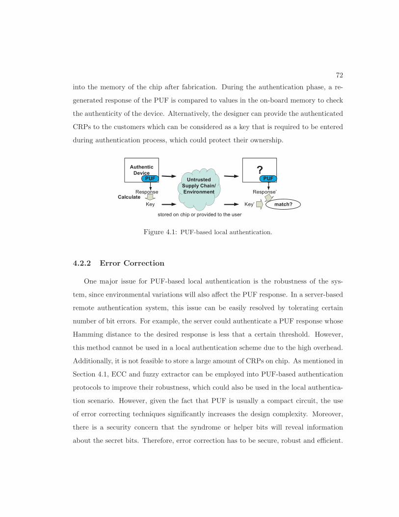
72
into the memory of the chip after fabrication. During the authentication phase, a re-
generated response of the PUF is compared to values in the on-board memory to check
the authenticity of the device. Alternatively, the designer can provide the authenticated
CRPs to the customers which can be considered as a key that is required to be entered
during authentication process, which could protect their ownership.
Authentic Device
Untrusted Supply Chain/Environment
PUF PUF
Key Key’
Response Response’ns
match?Calculate
?
stored on chip or provided to the user
Figure 4.1: PUF-based local authentication.
4.2.2 Error Correction
One major issue for PUF-based local authentication is the robustness of the sys-
tem, since environmental variations will also affect the PUF response. In a server-based
remote authentication system, this issue can be easily resolved by tolerating certain
number of bit errors. For example, the server could authenticate a PUF response whose
Hamming distance to the desired response is less that a certain threshold. However,
this method cannot be used in a local authentication scheme due to the high overhead.
Additionally, it is not feasible to store a large amount of CRPs on chip. As mentioned in
Section 4.1, ECC and fuzzy extractor can be employed into PUF-based authentication
protocols to improve their robustness, which could also be used in the local authentica-
tion scenario. However, given the fact that PUF is usually a compact circuit, the use
of error correcting techniques significantly increases the design complexity. Moreover,
there is a security concern that the syndrome or helper bits will reveal information
about the secret bits. Therefore, error correction has to be secure, robust and efficient.

73
In a typical error correction setting for PUF, during an initialization phase, a PUF
response is generated and the error correcting syndrome is computed based on this
response. The syndrome or helper data is public information which is later sent to the
PUF along with the challenges to perform correction on response bits. Equivalently, the
syndrome can be stored locally on chip. To re-generate the same PUF output, the PUF
first produces a response from the circuit. Then, the PUF uses the syndrome from the
initialization step to correct any errors in the circuit output. In this way, the PUF can
consistently reproduce the output from the initialization step if the device is authentic.
However, in most of previous works on correcting PUF responses, the area complex-
ities of the ECCs or the fuzzy extractors were not considered and there was no detailed
explanation on how to choose the algorithm and the parameters [38, 39]. In fact, the
implementation costs and hardware overheads of the commonly used ECCs are relative-
ly high, compared to the PUF circuit [52]. Besides of using ECC or fuzzy extractor,
other error correcting methods have also been exploited in the literature. The method
of utilizing majority voting on reducing errors has been demonstrated in [53]. The use
of repetition codes along with conventional syndrome generation using XOR masking
has been proposed for PUFs in [41]. Soft-decision encoders and decoders have also been
employed to correct PUF response errors [54]. However, the hardware implementations
of these methods have been only based on FPGAs and the area complexities have not
been addressed [53, 41, 54, 55]. Furthermore, authentications using pattern matching
algorithms [52, 51] need to maintain a database to store pattern information, which are
also not suitable for local authentication. In contrast to the above works, this chapter
proposes a novel secure, reliable and efficient error correcting method which can be used
for PUF-based local authentication.

74
4.3 Two-Level FSM Architecture
This section presents a basic two-level FSM scheme which could be used for PUF-
based authentication, IP binding, and IC metering. The general concept is illustrated in
the state transition graph (STG) of Figure 4.2. The PUF response and an authentication
key (i.e., Key in Figure 4.2) are used to determine the state of the FSM. The PUF
response is the input of the first level FSM, while key is the input of the second level
FSM. The first level FSM is designed to transit to a unique intermediate state for each
unique PUF response. Only if the actual PUF response is the same as the desired
PUF response, the FSM will enter into the correct intermediate state. Furthermore,
only one key value will transit the second level FSM from a certain intermediate state
to the desired state (i.e., Auth in Figure 4.2). The desired state then can be used to
authenticate the circuit or activate the correct functionality of certain blocks. Basically,
this architecture generates unique mapping pairs between PUF response and key, i.e.,
(Ri,Ki).
Auth.
Key
S0
K1S2
S1
Si
KKKKKKK1
AA
R1
S2N
R2
Ri
R2N
K2
Ki
K2NInitial
PUF Response
Figure 4.2: Two-level FSM.
It is important to note that (Ri,Ki) can be arbitrarily designed. Thus, all such
possible pairs are only known to the designer. For an N -bit PUF response, there will be
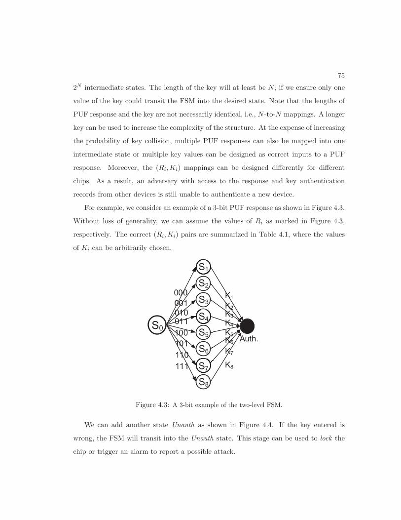
75
2N intermediate states. The length of the key will at least be N , if we ensure only one
value of the key could transit the FSM into the desired state. Note that the lengths of
PUF response and the key are not necessarily identical, i.e., N -to-N mappings. A longer
key can be used to increase the complexity of the structure. At the expense of increasing
the probability of key collision, multiple PUF responses can also be mapped into one
intermediate state or multiple key values can be designed as correct inputs to a PUF
response. Moreover, the (Ri,Ki) mappings can be designed differently for different
chips. As a result, an adversary with access to the response and key authentication
records from other devices is still unable to authenticate a new device.
For example, we consider an example of a 3-bit PUF response as shown in Figure 4.3.
Without loss of generality, we can assume the values of Ri as marked in Figure 4.3,
respectively. The correct (Ri,Ki) pairs are summarized in Table 4.1, where the values
of Ki can be arbitrarily chosen.
S3000001010011100101110111
K2
K1
K5K6
K7
K8
Auth.
S7
S4
S1
S0
S2
S5
S6
S8
K3K4
Figure 4.3: A 3-bit example of the two-level FSM.
We can add another state Unauth as shown in Figure 4.4. If the key entered is
wrong, the FSM will transit into the Unauth state. This stage can be used to lock the
chip or trigger an alarm to report a possible attack.

76
Table 4.1: Key Values Can Successfully Authenticate the Corresponding PUF ResponseRi correct Ki
000 K1
001 K2
010 K3
011 K4
100 K5
101 K6
110 K7
111 K8
Auth.
Unauth.
Key
S0
K1≠K1
S2
S1
Si
≠KKK1
KKKKKKK1
U
R1
S2N
R2
Ri
R2N
K2
Ki
K2N
≠K2
≠K2N
≠KiInitial
PUF Response
Figure 4.4: Two-level FSM that also has a lock or alarm state.

77
The global flow of the local authentication scheme by utilizing the proposed tech-
nique is shown in Figure 4.5. For example, Company X designs the circuit and integrates
a PUF and the self-correcting FSM into the design. The (Ri,Ki) pairs are designed at
this stage. After that, Company X sends the detailed manufacturable design specifica-
tions to Foundry Y who makes the mask and manufactures multiple chips implementing
this design. Each chip will be uniquely locked after fabrication due to the inter-chip
variations of the PUFs. For each chip, the PUF response needs to be tested, which can
be conducted by either Foundry Y or Company X if Foundry Y sends the manufactured
chips back to Company X. If the tests are done by Foundry Y, the PUF responses should
be sent back to Company X. According to the PUF response (which will be considered
as the desired PUF response for the authentication phase), only Company X has knowl-
edge of calculating the key for entering into the correct authenticated state. The key
could be programmed by another honest vendor after the chips have been fabricated or
sold to the customer, i.e., Company Z. Therefore, the correct key is a strong proof of
ownership. At the beginning of the authentication phase, the FSM enters into an inter-
mediate state based on the variability-induced response of PUF, as shown in Figure 4.6.
Only Company Z, who has the possession of the correct key, can authenticate the chip.
The global flow can also prevent the ICs piracy from overbuilding, as modern chip
designs are usually outsourced for fabrication. For example, it is conceivable that a
dishonest manufacturing plant could create more chips than ordered and sell the addi-
tional chips at a lower cost, subverting the profits of the legitimate owner. However, by
employing the proposed two-level FSM, over-produced chips that without the correct
keys cannot function properly, since the manufacturing plant (Foundry Y, for example)
does not know the correct (Ri,Ki) pairs.

78
X SemiconductorIC & PUF Design
Manufacture chips
Test PUF, calculate Key for each chip
Chip Authentication
Y Foundries
X Semiconductor
Z Systems, Inc
Figure 4.5: Typical design flow of a PUF-based local authentication system.
4.4 Error Correction based on the Two-Level FSM
4.4.1 Self-Correcting Functionality
We propose a novel FSM structure which not only has the capability for PUF-based
authentication, but also could correct certain number of PUF response bit errors, caused
due to environmental variations, to improve the robustness.
The two-level FSM structure presented in Section 4.3 can be extended to incor-
porate the error correcting functionality by allowing a second key attempt, as shown
in Figure 4.6. For instance, in the conventional two-level FSM authentication scheme,
if the PUF response varies due to environmental noise, the FSM will enter into a dif-
ferent intermediate state and the device cannot be authenticated with the correct key.
The problem can be solved by introducing a pathway from intermediate state S′i to the
authenticated state, where S′i represent a state whose Hamming distance of the corre-
sponding PUF response to the correct PUF response is less than or equal to m bits.
Note that S′i and Sj as shown in Figure 4.6 may represent multiple candidate states. If
the PUF response varies within m bits in the first level of the FSM structure, the second
attempt of the correct key Ki will bring the FSM back into the desired intermediate

79
state Si. The advantage of the proposed approach is the inherent redundancy built into
the self-correcting FSM by contiguously entering the key twice that eliminates the need
for an extra error correcting code. We can also design a scheme that the key will always
be internally entered to the FSM twice.
Si
HD=0 Ki
Ki
≠KiKi
HD: Hamming Distance between Actural PUF Response Ri and Correct Response
SiAuth.
Unauth.
S0
Sj
′
KeyPUF Response
1 HD m
HD>m
Figure 4.6: Two-level FSM can fix up to m-bit intra-chip errors (i.e., 1 ≤ HD ≤ m bit).
A 3-bit example of such a structure is shown in Figure 4.7. For example, if the
response of the PUF has been tested to be 010 during the enrollment phase, the designer
can calculate the correct key as K3. However, during the authentication phase, the PUF
response may vary 1 bit due to environmental variations, e.g., 000 instead of 010. In the
proposed structure, the FSM could transit into the desired black state S3 from the grey
state S1 by entering the correct key K3 for the first time. Then, if the authenticated user
enters K3 once more, the FSM will transit to the authenticated state. For other PUF
responses that have Hamming distances of 2 or greater, K3 would not be able to bring
the FSM back into the authenticated state. Note that only the edges associated with
K3 are shown in the STG, while other edges are omitted in Figure 4.7. The complete
next state table of the FSM design is presented in Table 4.2.
Similar to error correcting codes or fuzzy extractor, adding the error correcting
functionality will degrade the level of security. The probability for the adversary to

80
S3000001010011100101110111
K3
K3
K3
K3
K3
K3
K3
K3
Auth.
Unauth.S7
S4
S1
S0
S2
KKKKKS5
KS6
S8
Figure 4.7: A simplified 3-bit example for the proposed scheme.
Table 4.2: Key Values Can Successfully Authenticate the Corresponding PUF Response withSelf-CorrectionPresent State Next State
K1 K2 K3 K4 K5 K6 K7 K8
S0 S1 S2 S3 S4 S5 S6 S7 S8
S1 Auth S2 S3 Unauth S5 Unauth Unauth Unauth
S2 S1 Auth Unauth S4 Unauth S6 Unauth Unauth
S3 S1 Unauth Auth S4 Unauth Unauth S7 Unauth
S4 Unauth S2 S3 Auth Unauth Unauth Unauth S8
S5 S1 Unauth Unauth Unauth Auth S6 S7 Unauth
S6 Unauth S2 Unauth Unauth S5 Auth Unauth S8
S7 Unauth Unauth S3 Unauth S5 Unauth Auth S8
S8 Unauth Unauth Unauth S4 Unauth S6 S7 Auth
Auth Auth Auth Auth Auth Auth Auth Auth Auth
Unauth Unauth Unauth Unauth Unauth Unauth Unauth Unauth Unauth

81
guess the key value for a given PUF response will increase from 12N
to 1+N2N
, if one bit
error can be corrected for an N -bit PUF response. More generally, for m bits correction
in anN -bit PUF response, 1+∑m
i=1
(Nm
)key values can bring a certain intermediate state
to the correct Auth state, while there are 2N possible key values in total. In the example
of Figure 4.7, 4 out of 8 possible key values can authenticate the corresponding PUF
response. The details of successful key values that can authenticate the corresponding
PUF response are presented in Table 4.3. For example, besides K3, another three key
values K1, K4, K7 can also authenticate the PUF response 010. However, when N is
large (e.g., N = 256), the value of 1+N2N
will still be very small for a 1-bit correction
scheme. Furthermore, a requirement for a practical PUF is that the PUF responses
should have a large inter-chip variation (50% Hamming distance ideally) so that even
in the presence of noise it is possible to distinguish responses originating from different
devices. Therefore, key collision of the proposed self-correcting approach would not be
an issue for PUF-based authentication. A set of distinguishable keys can be obtained
for different chips even if the (Ri,Ki) pairs are designed equivalently. Moreover, as
discussed in Section 4.3, we can increase the length of key to improve the security.
Table 4.3: Key Values Can Successfully Authenticate the Corresponding PUF Response withSelf-Correction
Ri correct Ki other successful Ki
000 K1 K2, K3, K5
001 K2 K1, K4, K6
010 K3 K1, K4, K7
011 K4 K2, K3, K8
100 K5 K1, K6, K7
101 K6 K2, K5, K8
110 K7 K3, K5, K8
111 K8 K4, K6, K7
4.4.2 Advantages
Generally speaking, if we want to correct up to m bits of an N -bit PUF response,∑mi=1
(Nm
)extra transition edges need to be inserted for each intermediate state in the

82
state transition graph of the conventional two-level FSM. A FSM is usually defined by
a 6-tuple (I,O, S, S0, F,G), where S is a finite set of internal states, I and O represent
finite set of inputs and outputs of the FSM, respectively, F is the next-state function,
G is the output function, and S0 is the initial state. However, the extra transition
edges introduced by the error correcting functionality only affect the next state logic
of the FSM, while the output logic and the size of state registers remain the same, as
shown in Figure 4.8. As a result, we can expect the extra design complexity would be
relatively small for the self-correcting FSM structure, which only involves an N -to-N
combinational logic synthesis. Furthermore, although there are 2N intermediate states
in the proposed two-level FSM, the state registers only need to store N +1 bits in total
(including S0, Auth, and Unauth). For examples, when N = 3 as shown in Figure 4.7,
only a 4-bit state registers are required, as there are 11 states in the design. Therefore,
the proposed self-correcting FSM scheme could enable lightweight yet reliable PUF-
based authentication.
Next State Logic
Output Logic
State RegistersClock
Next StatePresent State
Input
Output
Only the next state logic needs to be redesigned
Figure 4.8: Only the output function of the FSM needs to be redesigned after adding theself-correcting functionality.
Another advantage is that the proposed scheme is more secure, compared to ECC
or fuzzy extractor. For example, in the applications of ECC, when testing a PUF
response, an error correcting syndrome (helper data, if for a fuzzy extractor) for that
response is also computed and saved for later use. The syndrome is information that
allows for correcting bit-flips in regenerated PUF outputs. The generated syndrome

83
is public information and can be stored anywhere (on-chip, off-chip, or remotely on a
server). Clearly, the syndrome reveals information about the PUF response. In general,
given the b-bit syndrome, attackers can learn at most b bits of the N -bit PUF response,
where b is less than N and is dependent on the specific parameters of the employed ECC.
The soft-decision syndrome coding scheme proposed in [54] could limit the amount of
leaked information to improve the security of PUF-based authentication. However, the
generated syndrome is still associated with the PUF response.
As opposed to these prior works, the key in our proposed self-correcting FSM is
not public that only the designer or the authenticated users have the knowledge of the
correct key. Furthermore, the fact that the PUF response and authentication key pairs
(Ri,Ki) can be arbitrarily designed, which are not based on any algorithm such as ECC
or fuzzy extractor, also enhances the security. In other words, even if the adversary
knows the PUF response (or key) in a (Ri,Ki) pair, it is still infeasible to guess the
corresponding key (or PUF response). Another advantage is that the successful key
values are not close, i.e., Hamming distance is less than a certain threshold. For example,
even for two pairs (Ri,Ki) and (Rj ,Kj) that the Hamming distance of the two PUF
responses Ri and Rj is only 1, the Hamming distance of the two keys Ki and Kj could
be very large. Additionally, along with the fact as discussed above that extraction of
the corresponding STG of the FSM is a computationally intractable task, the proposed
scheme could achieve a very high level of security.
4.5 Other Applications
In fact, the proposed self-correcting two-level FSM can be extended for other appli-
cations. In this section, we discuss a number of other possible applications.

84
4.5.1 Two-Factor Authentication
The proposed self-correcting two-level FSM can also be used for the so-called two-
factor authentication [56]. The challenge of a PUF is combined with the key to achieve
stronger hardware protection. The authenticated device, correct PUF challenge, and
correct key are required for the two-factor authentication. In other words, the (Ri,Ki)
pair is extended to (Ci, Ri,Ki). The state of the proposed two-level FSM is determined
by Ri and Ki, while Ri can be calculated by the challenge Ci for a given PUF. However,
PUF is a one-way function in the sense that it is hard to reconstruct the challenge
from the response. Therefore, even if the adversary knows the desired (Ri,Ki) pair,
it is still infeasible for the adversary to compromise the device without knowing the
correct challenge. Additionally, as described in Section 4.3, the (Ri,Ki) pairs can be
designed differently for different devices. As a result, (Ci, Ri) and (Ri,Ki) pairs will be
unique for each chip. The security can be greatly improved by the proposed two-factor
authentication. The security properties are summarized below:
(a) The device cannot be duplicated.
(b) The user is unable to authenticate without the device.
(c) The device cannot be used by someone else to successfully authenticate as the
user without the correct key.
(d) An adversary with access to the response and key authentication records from
other devices is still unable to authenticate a new device without the correct
challenge.
(e) The device does not need to store any information.
4.5.2 Signature Generation
The proposed self-correcting FSM architecture can also be utilized for reliable sig-
nature generation. The FSM can be modified as shown in Figure 4.9 to regenerate

85
the same PUF output, which would be more straightforward from the error correction
aspect. Instead of having two states (i.e., Auth and Unauth) at the last stage, the FSM
structure can be extended to enable an N -bit output by adding extra 2N output states
(OSs) at the last stage. Note that OS′i and OSj may represent multiple states, while
R′i and Rj may represent multiple incorrect PUF responses. Each output state OSi will
generate a unique output Ri, which corresponds to the desired PUF response. For ex-
ample, if the actual PUF response R′i vary within a tolerated range as the correct PUF
response Ri, the FSM will enter into an intermediate state S′i. By adding the transition
edges of the proposed self-correcting functionality into the STG, the FSM could transit
to the desired intermediate state Si by entering the correct key Ki for the first time.
When entering Ki the second time, the FSM will transit into OSi and the correct PUF
response Ri will be generated. Key values other than Ki cannot bring the FSM to the
last stage of the FSM from state Si. As a result, the same PUF response cannot be
regenerated. In this case, the key value can be made public which will be similar to the
functionality of syndrome in ECC or helper data in fuzzy extractor. As mentioned in
Section 4.4, it is still infeasible to predict the corresponding PUF response even if the
adversary knows the key value.
Si
HD=0 Ki
Ki
Ki
HD>m
1 HD m SiS0
Sj
′
KeyPUF Response
i
Kjjjj
′
Ri
RiRR
RjRR
′
OSi
Output
OSi
OSj
′
Figure 4.9: Reliable signature generation by utilizing the self-correcting FSM.
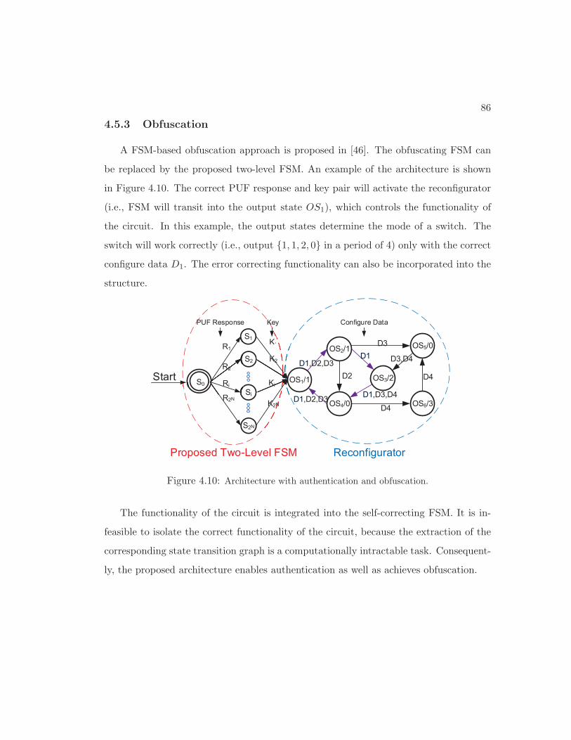
86
4.5.3 Obfuscation
A FSM-based obfuscation approach is proposed in [46]. The obfuscating FSM can
be replaced by the proposed two-level FSM. An example of the architecture is shown
in Figure 4.10. The correct PUF response and key pair will activate the reconfigurator
(i.e., FSM will transit into the output state OS1), which controls the functionality of
the circuit. In this example, the output states determine the mode of a switch. The
switch will work correctly (i.e., output {1, 1, 2, 0} in a period of 4) only with the correct
configure data D1. The error correcting functionality can also be incorporated into the
structure.
Proposed Two-Level FSM Reconfigurator
D1,D2,D3D1
D1,D3,D4D1,D2,D3
D2 D4
D4
D3
D3,D4
Key
S0
K1
S2
S1
Si
K1R1
S2N
R2
Ri
R2N
K2
Ki
K2N
PUF Response
Start OS1/1
OS2/1
OS4/0
OS3/2
OS6/3
OS5/0
Configure Data
Figure 4.10: Architecture with authentication and obfuscation.
The functionality of the circuit is integrated into the self-correcting FSM. It is in-
feasible to isolate the correct functionality of the circuit, because the extraction of the
corresponding state transition graph is a computationally intractable task. Consequent-
ly, the proposed architecture enables authentication as well as achieves obfuscation.

87
4.5.4 Correcting Other Errors
Although the proposed design of self-correcting two-level FSM is tailored for PUF-
based local authentication, this technique is not limited to correcting PUF response
errors. For example, the two-level FSM can be used for correcting communication
errors, where the key in our design will be treated as the syndrome in an ECC. The
proposed FSM architecture is also applicable to authentication for the Internet of Things
(IoT), where security is an important concern. As discussed in Section 4.4, the proposed
error correcting method could achieve higher security than the commonly used ECC or
fuzzy extractor, as syndrome will leak information of the secret bits to the adversary,
while (Ri,Ki) pairs in the two-level FSM can be arbitrarily chosen.
4.6 Hardware Implementation
In this section, we present the performance of the proposed two-level self-correcting
FSM. All the circuits are synthesized using Synopsys Design Compiler with optimization
parameters set for minimum area and mapped to a 65 nm standard cell library. Note
that we use a same bit-length for the PUF response and key in our implementations.
We first examine the performance with respect to the PUF response bit-length N , and
the number of tolerated error bits m. Then we compare the proposed error correcting
technique to one commonly used ECC for PUF-based authentication, i.e., the BCH
codes.
4.6.1 Area and Power
Table 4.4 and Table 4.5 show the area and power consumptions of the FSM as shown
in Figure 4.6, respectively, for different design parameters (i.e., N and m). Note that
when m = 0, the implemented structure is reduced to the FSM without self-correction
as shown in Figure 4.4. The results include average area and power overheads over a
number of different implementations, where the PUF response and key value mappings

88
are randomly designed (include both simple bitwise comparison and highly random
perturbation).
Table 4.4: Area (Gate Count) of the Proposed Self-Correcting FSM that Can Correct m Bitsof an N -Bit PUF Response
mN
4 8 16 32 64 128
0 70 114 197 367 709 13991 85 134 235 470 919 18102 147 265 507 985 19093 281 514 994 19634 519 1009 20315 534 1018 20426 537 1038 20497 541 1045 2061
Table 4.5: Power (μW ) of the Proposed Self-Correcting FSM that Can Correct m Bits of anN -Bit PUF Response
mN
4 8 16 32 64 128
0 0.60 0.95 1.66 3.03 5.79 11.441 0.63 1.00 1.91 3.61 6.83 13.472 1.12 2.08 3.80 7.47 14.553 2.11 3.87 7.61 15.144 3.93 7.87 15.585 3.97 8.01 15.866 4.07 8.19 16.027 4.13 8.28 16.16
As expected, the area and power consumptions are not very significant. For example,
the area of the proposed FSM for a 128-bit PUF response with 7 bits error correction
is only equivalent to 2061 NAND2 gates, while the power consumption is about 16μW .
As expected, the area and power consumptions are not very significant. For example,
the area of the proposed FSM for a 128-bit PUF response with 7 bits error correction
is only equivalent to 2061 NAND2 gates, while the power consumption is about 16μW .
This can be compared to 1399 gates and 11μW with no error correction for a 128-bit
PUF response.
For better illustrations, we plot the gate counts for m = 0 (without self-correction)
and m = 2 (with 2 bits error correction) as shown in Figure 4.11. It can be observed

89
that when the bit-length N is doubled, the area is also almost doubled for a fixed m.
The power consumption exhibits a similar trend.
0200400600800
100012001400160018002000
8 16 32 64 128
Gat
e C
ount
N
2 bits errorcorrectionno correction
Figure 4.11: Area (gate count) for different bit-length N without self-correction and with 2bits error correction.
We also plot the gate counts for different m for N = 64 as shown in Figure 4.12,
which is normalized to the gate count of the FSM when m = 0 and N = 64. It can
be seen that the overhead is about 30% for adding 1-bit error correcting functionality
into the conventional two-level FSM. However, as m increases, the additional overhead
in area or power consumption becomes less and less. For example, the overhead is 47%
when m = 7, while the overhead is already 39% when m = 2. Therefore, we can expect
that overhead of the proposed self-correcting FSM would be reasonable even for a large
m. Note that we can draw similar conclusions for area and power consumptions of the
FSM with other values of N , as shown in Table 4.4 and Table 4.5.
4.6.2 Comparison to BCH Codes
As illustrated in Section 4.2, the hardware implementation of the error correcting
techniques in prior works on PUF-based authentication were either not considered or
only implemented on FPGAs. However, error correcting techniques that incur relative-
ly large overhead, compared to PUF circuit, would not be suitable for lightweight and
low-cost devices. Furthermore, to the best of our knowledge, there is no other work on

90
1
1.1
1.2
1.3
1.4
1.5
0 1 2 3 4 5 6 7
Nor
mal
ized
Gat
e C
ount
m
Figure 4.12: Normalized area (gate count) for different m (N = 64).
efficient hardware implementation of error correcting method that is particularly well
suited for PUF-based authentication in the literature. As a result, it is important to ex-
amine the performance comparison with other state-of-the-art low-cost error correcting
techniques. In order to achieve fair comparison, we also synthesized comparable BCH
decoders using the same 65 nm standard cell library. The area and power consumptions
for different parameters are presented in Table 4.6 and Table 4.7, respectively. Note
that the values of N are chosen to 1 less than 2n, as that is the highest value permitted
in the finite field of 2n.
Table 4.6: Area (gate count) of the BCH Codes
mN
31 63 127
1 1031 1370 17602 1816 2410 30923 2612 3460 44354 3419 4519 57895 4231 5580 71536 5039 6646 85277 5854 7720 9908
It can be seen from our experimental results that the proposed self-correcting FSM
consumes about 2× to 10× less area and about 20× to 100× less power than the BCH
codes. Therefore, it can be concluded that the cost of correcting PUF response can be

91
Table 4.7: Power (μW ) of the BCH Codes
mN
31 63 127
1 181.67 228.86 286.602 319.54 401.99 503.073 458.77 576.39 721.184 598.77 751.31 940.615 739.70 926.44 1161.156 881.98 1102.21 1382.337 1024.90 1238.89 1604.58
significantly reduced by the proposed approach. Particularly, the power consumption
can be reduced to 1% ∼ 5% of the BCH codes. Additionally, as discussed above, the
extra overhead of the proposed self-correcting FSM will be small for a large number of
tolerated error bits m. However, for the BCH codes, it can be observed from Table 4.6
and Table 4.7 that both the area and power consumptions increase linearly with the
number of tolerated error bits, which is also consistent with the results in [57]. Therefore,
we can expect that the area consumption of the proposed method will be significantly
less than the BCH codes for a large m.
Furthermore, it is important to note that the proposed FSM architecture not only
corrects the errors, but also has the capability for PUF-based authentication. If we only
consider the design complexity for the error correcting functionality itself, the proposed
approach would be much more lightweight and low-cost compared to the BCH codes.
For example, we consider the overhead of introducing 4 bits error correcting functional-
ity to the two-level FSM without error correction. The area and power overhead results
for both the proposed self-correction FSM and the BCH codes are normalized to the
cost of the two-level FSM without error correction, as shown in Figure 4.13 and Fig-
ure 4.14, respectively. It can be seen that the normalized overheads of the BCH codes
are significantly greater than those of the proposed self-correcting FSM. For instance,
when N = 128 and m = 4, the normalized area overhead for the proposed self-correcting

92
FSM is 9× less than the BCH codes, while the normalized power overhead for the pro-
posed self-correcting FSM is 167× less than the BCH codes. It can also be observed
that the overhead incurred by BCH codes will decrease as N increases. However, the
length of PUF response used for authentication is usually relatively small (N ≤ 256).
Therefore, it can be concluded that the overhead of the proposed self-correcting FSM
is significantly less than the BCH codes for the PUF-based authentication.
0123456789
10
32 64 128
Nor
mal
ized
Are
a
N
Proposed Self-Correcting FSM
BCH Codes
Ove
rhea
d Fa
ctor
Figure 4.13: Normalized area overheads of introducing 4 bits error correcting functionality forthe proposed self-correcting FSM and the BCH codes.
020406080
100120140
32 64 128
Nor
mal
ized
Pow
er
Ove
rhea
d Fa
ctor
N
Proposed Self-Correcting FSM
BCH Codes
Figure 4.14: Normalized power overheads of introducing 4 bits error correcting functionalityfor the proposed self-correcting FSM and the BCH codes.

93
4.7 Conclusion
This chapter has presented a novel two-level self-correcting FSM, which can be used
for PUF-based authentication while tolerating a certain number of bit errors that are
generated by environmental variations. The applications of the proposed method for
local authentication and reliable signature generation have also been discussed. The
performances of the proposed two-level self-correcting FSM with respect to the PUF
response bit-length and the number of tolerated error bits have been studied. We have
also shown that the proposed technique achieves significantly lower cost than the error
correcting methods that are previously used for PUF-based authentication.

Chapter 5
Obfuscating DSP Circuits via
High-Level Transformations
5.1 Introduction
Digital Signal Processing (DSP) plays a critical role in numerous applications such as
video compression, portable systems/computers, multimedia, wired and wireless com-
munications, speech processing, and biomedical signal processing. However, as electron-
ic devices become increasingly interconnected and pervasive in people’s lives, security,
trustworthy computing, and privacy protection have emerged as important challenges
for the next decade. Therefore, DSP system designers have to pay more attention to
the security perspective of DSP circuits, since the adversary can easily learn the func-
tionality using massive attacking methods.
The problem of hardware security is a serious concern that has led to a lot of work on
hardware prevention of piracy and intellectual property (IP), which can be broadly clas-
sified into two main categories: 1) authentication-based approach, and 2) obfuscation-
based approach. The authentication-based approaches include physical unclonable func-
tions (PUFs) based authentication [38], digital watermarking [58, 59, 60, 61], key-locking
94

95
scheme [62, 63], and hardware metering [42]. The focus of this chapter is on obfuscation,
which is a technique that transforms an application or a design into one that is func-
tionally equivalent to the original but is significantly more difficult to reverse engineer.
Some hardware protection methods are achieved by altering the human readability of
the hardware description language (HDL) code, or by encrypting the source code based
on cryptographic techniques [64]. Recently, a number of hardware obfuscation schemes
have been proposed that modify the finite-state machine (FSM) representations to ob-
fuscate the circuits [65, 66, 45].
However, to the best of our knowledge, no obfuscation-based IP protection approach
has been proposed specifically for DSP circuits in the literature. Our work, for the first
time, presents design of obfuscated DSP circuits via high-level transformations that are
harder to reverse engineer. From this standpoint of view, a DSP circuit is more secure,
if it is harder for the adversary to discover its functionality even if the adversary can
physically tamper the device. In other words, a high level of security is achieved if the
functionality of a DSP circuit is designed to be hidden from the adversary.
The key contribution of this chapter is a novel approach to design obfuscated DSP
circuits by high-level transformations during the design stage. The DSP circuits are
obfuscated by introducing a finite-state machine (FSM) whose state is controlled by a
key. The FSM enables a reconfigurator that configures the functionality mode of the
DSP circuit. High-level transformations lead to many equivalent circuits and all these
create ambiguity in the structural level. High-level transformations also allow design of
circuits using same datapath but different control circuits. Different variation modes can
be inserted into the DSP circuits for obfuscation. While some modes generate outputs
that are functionally incorrect, these may represent correct outputs under different
situations, since the output is meaningful from a signal processing point of view. Other
modes would lead to non-meaningful outputs. The initialization key and the configure
data must be known for the circuit to work properly. Consequently, the proposed

96
design methodology leads to a DSP circuit that is both structurally and functionally
obfuscated.
Furthermore, the approach presented in the chapter will prevent piracy from over-
production and mask theft, because the manufacturer would not have access to either
the initialization key or the configure data. These keys could be programmed by anoth-
er honest vendor after the chips have been fabricated or provided to the customers by
the designer. Therefore, overproduced chips without the correct keys cannot function
properly.
5.2 Hiding Functionality by High-Level Transformations
High-level transformations [67] have been known for a long time and have been used
in a wide range of applications, such as pipelining [68], interleaving [68], folding [69],
unfolding [70] and look-ahead transformations (e.g., quantizer loops [71], multiplexer
loops [72, 73], relaxed look-ahead [74], annihilation reordering look-ahead [75]), and
have been used in synthesis of DSP systems [76]. These techniques can be applied at
the algorithm or the architecture level to achieve a tradeoff among different metrics
of performance, such as area, speed, and power [77]. However, the use of high-level
transformations from a security perspective has not been studied before. High-level
transformations alter the structure of a DSP circuit, while maintaining the original
functionality. These transformations may lead to architectures whose functionalities
are not obvious. Take an extreme case for example, many filters can be folded into one
multiply-accumulator (MAC), but their functionalities are not the same. In other words,
one MAC with proper switches can implement many different digital filters. Therefore,
we can conclude that high-level transformations naturally provide a means to obfuscate
DSP circuits both structurally and functionally. Structural obfuscation and functional
obfuscation are defined as follows:

97
(a) Structural Obfuscation: any algorithm can be implemented by a family of architec-
tures by using high-level transformations. These architectures enable structural
obfuscation where the functionalities of the algorithms can be hidden. This can
be considered as a ”passive” model from attacker’s perspective.
(b) Functional Obfuscation: this is realized by encrypting the normal functionality of
a DSP circuit with one or more sets of keys. The DSP circuit cannot function
correctly without the keys. This corresponds to an ”active” model from attacker’s
perspective.
Folding is such an example of high-level transformation which could be utilized to
achieve design obfuscation. The folding transformation generates folded variants based
on the folding set, which is the reverse of the unfolding transformation [70]. The choice
of folding set is critical to the performance of the folded structure, since an appro-
priate choice of folding order can lead to an architecture with lower area and power.
Folding sets can be designed intuitively to meet the performance requirements or can
be obtained from a high-level synthesis system [76]. The details and other examples
(e.g., interleaving) of how to hide the functionalities of DSP circuits by high-level trans-
formations are described in [78, 79]. We can observe that: 1) Circuits with different
functionalities can have a similar structure, and circuits with the same functionality may
have very different structures; 2) Structural obfuscation can be achieved by high-level
transformations; 3) If the switch instances are invisible to the adversary, then the DSP
systems will be harder to reverse engineer, since the functionality of a DSP circuit is
not obvious due to obfuscation achieved by high-level transformations. As a result, the
adversary who only has knowledge of the structural information but lacks knowledge of
the switch instances cannot easily discover the functionality of a DSP circuit.
As an example, we consider a 3rd-order IIR digital filter given by transfer function
H(z) = 1+m2z−1+m3z−2
1−m0z−2−m1z−3 , as shown in Figure 5.1. The coefficients mi correspond to the
multiplication Mi. We assume the availability of one 1-stage pipelined adder and one
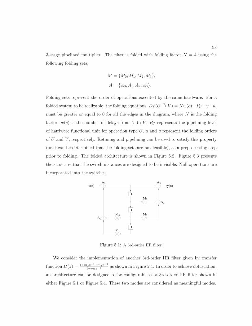
98
3-stage pipelined multiplier. The filter is folded with folding factor N = 4 using the
following folding sets:
M = {M0,M1,M2,M3},A = {A0, A1, A2, A3}.
Folding sets represent the order of operations executed by the same hardware. For a
folded system to be realizable, the folding equations, DF (Ue→ V ) = Nw(e)−PU+v−u,
must be greater or equal to 0 for all the edges in the diagram, where N is the folding
factor, w(e) is the number of delays from U to V , PU represents the pipelining level
of hardware functional unit for operation type U , u and v represent the folding orders
of U and V , respectively. Retiming and pipelining can be used to satisfy this property
(or it can be determined that the folding sets are not feasible), as a preprocessing step
prior to folding. The folded architecture is shown in Figure 5.2. Figure 5.3 presents
the structure that the switch instances are designed to be invisible. Null operations are
incorporated into the switches.
D
D
D
u(n) y(n)
M0
M1
M2
M3
A2
A3A1
A0
Figure 5.1: A 3rd-order IIR filter.
We consider the implementation of another 3rd-order IIR filter given by transfer
function H(z) = 1+m2z−1+m3z−2
1−m1z−3 as shown in Figure 5.4. In order to achieve obfuscation,
an architecture can be designed to be configurable as a 3rd-order IIR filter shown in
either Figure 5.1 or Figure 5.4. These two modes are considered as meaningful modes.

99
{0}
3D D D D 3D 2DD
y(n)
u(n){1}
{3}{0,2}
{1}
{1,3}{2}
{3}
{0}{0,2}
Figure 5.2: A folded structure of the 3rd-order IIR filter in Fig. 1. The switch instance ”i”corresponds to clock cycle 4l + i.
3D D D D 3D 2DD
y(n)
u(n) Ø
ØØ
Figure 5.3: A folded structure of the 3rd-order IIR filter with invisible switches.

100
In fact, a folded architecture of Figure 5.4 using the following folding sets can be
obtained by assigning different switch instances to the structure in Figure 5.3, which is
shown in Figure 5.5.
M = {∅,M1,M2,M3},A = {∅, A1, A2, A3}.
The folding factor is 4, while there are only 3 multipliers and 3 adders in the DSP
circuit. Therefore, if we consider the functionality of Figure 5.4 as the desired mode,
one computation cycle is wasted every 4 cycles. The latency will also be increased. Note
that we could use clock gating techniques to reduce the power for the null operation
cycles.
D
D
D
u(n) y(n)
M1
M2
M3
A3
A2A1
Figure 5.4: Another 3rd-order IIR filter.
3D D D D 3D 2DD
y(n)
u(n) Ø
ØØ{1}
{3}{0}
{2}
{0}
{0}{1}{2} {3}
{3}{1,2}
{0}
Figure 5.5: A folded structure of the 3rd-order IIR filter in Figure 5.4. The switch instance”i” corresponds to clock cycle 4l + i.

101
However, we can extend the periodicity of the switches to overcome the hardware
underutilization. For instance, we can fold the 3rd-order IIR filter in Figure 5.4 by
folding factor 3 with the folding sets:
M = {M3,M1,M2},A = {A2, A1, A3}.
The folded structure is shown in Figure 5.6. We can accommodate the two meaning-
ful modes with no increase in latency for the second mode by extending the periodicity
of the switches to the least common multiple of the folding factors of the two modes
(i.e., lcm(3,4)=12). Similar extensions of switch periods have been considered in de-
sign of digit-serial DSP architectures [80]. For example, switch instance 4l + i can be
rewritten as 12l+ i, 12l+4+ i, and 12l+8+ i, for i ranging from 0 to 3, in Figure 5.2;
while switch instance 3l + i can be rewritten as 12l + i, 12l + 3 + i, 12l + 6 + i, and
12l + 9 + i, for i ranging from 0 to 2, in Figure 5.6. As a result, for each meaningful
mode as the desired mode, the latency remains the same as the original folded struc-
ture. This is achieved by increasing the complexity of the switch and the expense of
hardware overhead associated with this step. The final obfuscated architecture for these
two meaningful modes is shown in Figure 5.7. The switch instances are obfuscated and
the two correct configurations of the switches correspond to two meaningful modes.
3D D D D 3D2D
y(n)
u(n)
{1}
{0}{2}
{1}{2} {0}
{0}
{1}
{2}
{1}
Figure 5.6: Another folded structure of the 3rd-order IIR filter in Figure 5.4. The switchinstance ”i” corresponds to clock cycle 3l + i.

102
3D D D D 3D 2DD
y(n)
u(n) Ø
ØØ
D
Figure 5.7: An obfuscated structure, which can be configurable as a 3rd-order IIR filter shownin either Figure 5.1 or Figure 5.4.
5.3 Obfuscated Design via High-Level Transformations
5.3.1 Secure Switch Design
From Section 5.2, it can be seen that the DSP circuits can be obfuscated via high-
level transformations by appropriately designing the switches in a secure manner. The
switches generated by high-level transformations are periodic N-to-1 switches. These
switches can be implemented as multiplexers (MUXs), whose control signals are obtained
from ring counters (as shown in Figure 5.8). Thus, the security of the switch relies upon
design of the ring counters such that the outputs of the ring counters can be obfuscated.
MUX
.
.
.
controlsignal
ringcounter
connection 1connection 2connection 3
connection k
connection 1connection 2connection 3
connection k
.
.
....
Figure 5.8: Switch implementation.
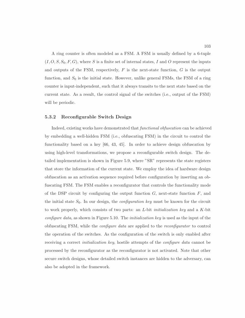
103
A ring counter is often modeled as a FSM. A FSM is usually defined by a 6-tuple
(I,O, S, S0, F,G), where S is a finite set of internal states, I and O represent the inputs
and outputs of the FSM, respectively, F is the next-state function, G is the output
function, and S0 is the initial state. However, unlike general FSMs, the FSM of a ring
counter is input-independent, such that it always transits to the next state based on the
current state. As a result, the control signal of the switches (i.e., output of the FSM)
will be periodic.
5.3.2 Reconfigurable Switch Design
Indeed, existing works have demonstrated that functional obfuscation can be achieved
by embedding a well-hidden FSM (i.e., obfuscating FSM) in the circuit to control the
functionality based on a key [66, 43, 45]. In order to achieve design obfuscation by
using high-level transformations, we propose a reconfigurable switch design. The de-
tailed implementation is shown in Figure 5.9, where ”SR” represents the state registers
that store the information of the current state. We employ the idea of hardware design
obfuscation as an activation sequence required before configuration by inserting an ob-
fuscating FSM. The FSM enables a reconfigurator that controls the functionality mode
of the DSP circuit by configuring the output function G, next-state function F , and
the initial state S0. In our design, the configuration key must be known for the circuit
to work properly, which consists of two parts: an L-bit initialization key and a K-bit
configure data, as shown in Figure 5.10. The initialization key is used as the input of the
obfuscating FSM, while the configure data are applied to the reconfigurator to control
the operation of the switches. As the configuration of the switch is only enabled after
receiving a correct initialization key, hostile attempts of the configure data cannot be
processed by the reconfigurator as the reconfigurator is not activated. Note that other
secure switch designs, whose detailed switch instances are hidden to the adversary, can
also be adopted in the framework.

104
F
G
SRclk
Reconfigurator
reset
resetstate
MUX
.
.
.
controlsignal
connection 1connection 2
connection kObfuscating
FSMconfigurationkey
(switch instances)
ring counterFSM
Figure 5.9: The complete reconfigurable switch design.
configuration key
(L+K)-bit
initialization key (L)-bit
configure data (K)-bit
Figure 5.10: Configuration key containing an initialization key and a configure data.

105
The number of possible variations of ring counters is limited by the length of the
configure data, K. We can create M variation modes of the original circuits that have
different functionalities, while log2M should be less than or equal to the length of config-
ure data, K. Different configure data can be mapped into the same mode. An example
of the mapping between the configure data and the associated modes is illustrated in
Table 5.1. Note that this only involves simple combinational logic synthesis.
Table 5.1: Switch ConfigurationsMode Configure Data1 data1, data22 data3... ..., ...M data{2K−1}, data{2K}
5.4 Generation of Variation Modes
5.4.1 Security Perspective of Variation Modes
The cost for an adversary to find the correct key of an obfuscated DSP circuit by
adopting the proposed architecture is not only dependent on the length of the configu-
ration key (L +K), but also on the number of required input-vectors for learning the
functionality of each variation mode (note that in this chapter, the inputs represent
the original inputs of the DSP circuits, while the key represents the data to control
the switches). For a certain variation mode, the adversary attempts to attack the D-
SP circuit by generating input-vectors until the functionality could be discovered. The
most intuitive way to mask the desired functionality is to modify the switch instances
arbitrarily. However, the functionality of the resulting structure may not be meaning-
ful from a signal processing point of view, which would be easier for the adversary to
distinguish whether the circuit is operating correctly. The numbers of required input-
vectors for these non-meaningful variation modes would be less than the numbers of
required input-vectors for meaningful variation modes. If one mode of a DSP circuit is

106
obfuscated to output a large portion of invalid values, the adversary can figure out this
mode is non-meaningful with a relatively small number of input-vectors.
The challenge of this problem is how to generate meaningful variation modes from
a signal processing point of view such that the DSP circuit can also be operated in a
reconfigurable manner. Most often, we perform a high-level transformation based on
the design requirements and constraints by taking an existing design and generating the
resulting design during high-level synthesis stage. We may continue to add variation
modes into the design, as discussed in Section 5.2. Some of the variation modes may
correspond to meaningful modes (e.g., different order filters or filters of same order with
different coefficients) which can be exploited for different applications, while others
correspond to non-meaningful modes.
Design of obfuscated DSP circuits requires extra efforts during the design phase.
In fact, variations of the algorithm (e.g., different folding sets) can also be utilized to
produce several obfuscated versions. Therefore, it is possible to generate meaningful
variation modes simultaneously with the high-level transformation during design stage
instead of modifying the switch instances after performing high-level transformations.
As a result, the variations of the structures are indeed obtained from the variations of the
selected algorithm. Furthermore, the secure switches can also be designed systematically
based on the variations of algorithms. Using this approach, the extra design efforts can
be reduced, while reconfigurable design with a number of different meaningful modes is
ensured.
Note that meaningful modes are not mandatory for the proposed obfuscated design.
While meaningful modes achieve higher security, obfuscation only with non-meaningful
modes could also attain considerable protection of the DSP circuit against reverse en-
gineering.

107
5.4.2 A Case Study: Hierarchical Contiguous Folding Algorithm
The variation modes are generated based on the selected transformation algorithm,
which are different for various high-level transformations. It is difficult to cover very
large number of existing high-level transformations in this chapter. We just present
an example to demonstrate how to generate variation modes. The proposed design
methodology can also be extended to other high-level transformations.
Hierarchical folding approach is a novel folding technique that combines folding of
M cascaded stages to one hardware block, and folding N operations inside each section
to a hardware functional unit, as shown in Figure 5.11. Two hierarchical folding algo-
rithms are presented in [78], which include hierarchical interleaved folding (HIF) and
hierarchical contiguous folding (HCF). In this section, we only address hierarchical con-
tiguous folding, while it is also applicable to hierarchical interleaved folding. Hierarchical
contiguous folding transformation executes all operations of one section before starting
execution of operations of next section. Reader is referred [78] for further details.
Alg1Alg0 AlgM-1Alg2u(n) y(n)...
(a) Unfolded structure
Algu(n)
(b) Folding
Same structure as M-interleaved, replace eachdelay by M delays of Algi
DF
Figure 5.11: (a) A DSP data-flow graph containing M cascaded stages. Block Algi representsi-th stage of the cascade. (b) A folded architecture where M stages are folded to same hardware.DF represents the number of folded delays.
Hierarchical contiguous folding transformation executes all operations of one section
before starting execution of operations of next section. The folding sets are described
as follows:
{X00 , X
01 , ...X
0N−1, X
10 , X
11 , ...X
1N−1, ..., X
M−10 , XM−1
1 , ...XM−1N−1 }, (5.1)

108
The operation Xji , i.e., the i-th operation of j-th block, will be executed at time Nj+ i.
The operations in a later section will be executed only after all the operations from the
previous section are completed. The algorithm is described below:
Hierarchical Contiguous Folding (HCF) Algorithm
1. Fold Algi by factor NM , with the folding set
{X0, X1, ...XN−1, ∅, ∅, ...∅}, where the number of null operations corresponds to
(NM −N).
2. Replace each switch s by s,s+N ,s+ 2N ,...s+ (M − 1)N .
3. Compute DF (Algj e→ Algj+1), for j = 0, 1, 2...M − 2, and use these folded edges
to replace the external inputs.
We propose an algorithm for obfuscation that generates variation modes by vary-
ing the number of sections in the cascade structure based on the HCF algorithm. For
example, if the number of sections for a DSP system is l, then the algorithm can be
described as below (the total number of operations is still NM , where M ≥ l).
Design Obfuscation Algorithm based on the HCF Algorithm
1. Fold Algi by factor NM , with the folding set
{X0, X1, ...XN−1, ∅, ∅, ...∅}, where the number of null operations corresponds to
(NM −N).
2. Replace each switch s by s,s+N ,s+ 2N ,...s+ (l− 1)N , and set switch instances
from lN to MN − 1 to null operations.
3. Compute DF (Algj e→ Algj+1), for j = 0, 1, 2...l− 2, and use these folded edges to
replace the external inputs.

109
If l = M , this algorithm reduces to the hierarchical contiguous folding algorithm.
From this algorithm, we can generate M meaningful modes correspond to l = 1, 2, ...,M .
Furthermore, the reconfigurator can also be designed based on the variations of the HCF
algorithm, which is a simple 2K-to-M combinational logic design problem. Note that
this algorithm can be easily extended to other types of DSP systems where the sub-
circuits are not directly connected.
5.5 Design Flow of the Proposed DSP Circuit Obfuscation
Approach
5.5.1 Design Methodology
In this section, we propose a novel DSP hardware protection methodology through
obfuscation by hiding functionality via high-level transformations. This approach helps
the designer to protect the DSP design against piracy. The detailed design flow is
described below:
Step 1: DSP algorithm. This step generates the DSP algorithm based on the
DSP application.
Step 2: High-level transformation selection. Based on the specific application,
appropriate high-level transformation should be chosen according to the performance
requirement (e.g., area, speed, power or energy).
Step 3: Obfuscation via high-level transformation. Selected high-level trans-
formations are applied simultaneously with obfuscation where variation modes, and
different configurations of the switch instances are designed.
Step 4: Secure switch design. The secure switch is designed based on the
variations of high-level transformations. Note that different configure data could be
mapped into the same mode, which only involves simple combinational logic synthesis.

110
Step 5: Two-level FSM generation. The reconfigurator and the obfuscating
FSM are incorporated into the DSP design as shown in Figure 5.9. The configuration
key is generated at this step.
Step 6: Design specification. This step includes the HDL and netlist generation
and synthesis of the DSP system.
After these design steps, designer sends the obfuscated design to the foundry that
manufactures the DSP circuit. By using the proposed design methodology, the manu-
facturer will not gain access to the desired functionality or the configuration key. Unau-
thorized copies of the obfuscated DSP circuits would provide little information to the
adversary. The relationship between the obfuscated design and the original design via
high-level transformation is illustrated in Figure 5.12. The only difference between the
obfuscated design and the original design via high-level transformation is the control of
the DSP circuit. The main datapath is unaltered. As a result, the critical path would
not increase for the obfuscated design. Furthermore, the proposed design methodology
does not require significant changes to established verification and testing flows. In fact,
the obfuscated DSP circuit with the correct key behaves just like the original circuit.
5.5.2 Architecture of the Obfuscated DSP Circuits
The complete system of the proposed obfuscated DSP circuit is illustrated in Fig-
ure 5.13. The reconfigurator will be enabled only by the correct initialization key. Only
the correct configure data leads to the desired design. A wrong configure data activates
an obfuscated mode (either a meaningful or non-meaningful). The obfuscating FSM
and a portion of non-meaningful variation modes (i.e., we denote as alarm modes) can
both be utilized for security check purpose. For example, some undesired modes in
Table 5.1 can be designed as alarm modes by adding another output signal to the com-
binational logic. We can improve the security by mapping a larger number of configure
data to this alarm mode, while keeping the portion of functional configure data to be

111
Datapath
DSPAlgorithm/Application
Control
Datapath
Control
ReconfiguratorObfuscating FSM
Design via High-Level
Transformation
ObfuscatedDesign via High-
LevelTransformation
Figure 5.12: Relationship between the obfuscated design and the original design.
relatively small. If the circuit continuously receives wrong initialization key or configure
data whose number exceeds the pre-defined threshold, the adversary is prevented from
further attempts of the configuration key by a denial of use block.
5.6 Security and Resiliency against Attacks
5.6.1 Attacks and Countermeasures
The goal of the proposed methodology is to ensure the designer’s intellectual proper-
ty would not be stolen against reverse engineering. Generally speaking, a hacker trying
to determine the functionality of a DSP circuit can resort to either of the following ways:
1) structural analysis of the netlist to identify and isolate the original design from the
obfuscated design or 2) simulation-based reverse engineering to determine functionality
of the design.

112
DSPAlgorithm/Application
Desired Design
MeaningfulObfuscated
DesignsNon-Meaningful
ObfuscatedDesigns
Obfuscated DesignsObtained by High-
Level Transformations
Correct?
Retry
RetryAttemptsExceeds
Threshold
Correct?
Denial ofUse
YesYes
YesNo
No
No
Initializationkey
Configuredata
YesEnterAlarmModes
ExceedsThreshold
Figure 5.13: Architecture of the proposed obfuscated DSP circuit.
Our proposed obfuscation methodology protects the hardware against the first type
of attack (i.e., structural analysis) from two perspectives: 1) structural obfuscation by
high-level transformation, and 2) integration with obfuscation modes. As presented in
Section 5.2, high-level transformations lead to structural obfuscation at the HDL level or
gate-level netlist. Without knowing the correct configuration of the switches, it is hard
for the adversary to learn the functionality of the original design. Furthermore, although
the obfuscating FSMs could be isolated, the obfuscation of configuration switches cannot
be separated from the original functionalities. Since the obfuscation variation modes are
integrated to the reconfigurator in the synthesized DSP circuit, the adversary cannot
remove the design obfuscation achieved by high-level transformations. Additionally,
meaningful variation modes also create ambiguity when the adversary performs the
structural analysis attacks.
For a simulation-based approach where random key vectors are sequentially applied
to take the circuit to the correct mode, the probability of discovering the configuration

113
key sequence is 12L+K for a circuit with a length-(L + K) configuration key sequence.
For example, the probability is only 5.4 × 10⁻²⁰ for a circuit with a length L = 32
initialization key sequence and a length K = 32 configure data sequence.
Moreover, the cost of the simulation based attack approach is also dependent on
the size of inputs. Various input patterns need to be tested to determine the complete
functionality of a DSP circuit. In practice, most DSP circuits will have considerable size
of inputs and the length of configuration keys can be made larger. Therefore, brute-
force attack for learning the key sequences and input/output patterns is computationally
infeasible.
5.6.2 Measure of Obfuscation Degree
Structural Obfuscation Degree (SOD)
Manual attacks can be performed by visual inspection and structural analysis. In
these types of manual attacks, the adversary has to analyze the RTL or gate-level
structure as well as the layouts. This is a weak attack, as the adversary has very little
chance of figuring out the obfuscation scheme for large DSP circuits.
The obfuscation degree of the structural obfuscation is dependent on the number
of independent switches (Ns), the period of switch instances after high-level transfor-
mations (P ), and the number of connections for each independent switch (Cm). To
estimate the obfuscation degree against these manual attacks, we propose a metric
called Structural Obfuscation Degree (SOD):
SOD =
Ns∏m=1
(Cm + 1)P , (5.2)
where the additional ”1” corresponds to the null operation. Note that a higher SOD
value implies better obfuscation, as the SOD value indicates the number of possible
functionalities generated by the combinations of these switches. A circuit is more secure,
if there is more ambiguity in the structure. For example, the SOD value of the structure

114
in Figure 5.3 can be calculated as 34 × 44 × 54 = 12, 960, 000 (excluding the output
switch), which is already very large.
For a small sub-circuit with a small SOD value, it may be feasible to figure out
the original functionality from the obfuscated design, as the number of combinations
is small and most of these combinations may result in non-meaningful functionalities.
However, the structure of a DSP circuit after high-level transformations usually has a
larger SOD value (as illustrated by the example above). Thus, it will be extremely hard
to distinguish the original functionality from other possible functionalities of these DSP
circuits.
Functional Obfuscation Degree (FOD)
The proposed methodology also achieves functional obfuscation by encrypting the
correct functionality with a key sequence. The cost for an adversary to discover the
correct key is dependent on the bit-length of the key (L+K), the number of meaningful
modes (Nm), the number of non-meaningful modes (Nn), and the size of input bits
(NI). To estimate the obfuscation degree against simulation based attacks, we propose
a metric denoted as Functional Obfuscation Degree (FOD):
FOD = f(NI)2L[Nm + αNn + β(2K −Nm −Nn)], (5.3)
where f(NI) represents the input cost coefficient that is the number of input vectors
required for learning the functionality of the DSP circuit, which is proportional to NI ;
and α, β represent the cost coefficients of learning a new non-meaningful variation
mode and learning a previously known mode compared to learning a new meaningful
mode, respectively. These coefficients are dependent on the particular applications. As
discussed in Section 5.4.1, it can be expected that they would follow the relation that
0 < β < α < 1. Future work will be directed towards validating the values of α and β
through experimental results. The higher the FOD value, more secure the obfuscated

115
design. Note that in practice, the computation cycles and the clock periods of the DSP
circuits would also affect the cost of simulation based attacks.
5.6.3 Improving the Security by Key Encoding
In the proposed obfuscation scheme, the key consists of two parts: initialization
key and configure data. However, in the scenario that the adversary has found a key
that can successfully pass the initialization but is still in an incorrect configuration, the
adversary will only try different configure data while fixing the initialization key. This
could weaken the scheme. An encoder could be added to improve the security of the
system, as shown in Figure 5.14. The encoder could be a Hash function, a linear feedback
shift register (LFSR), or a Physical Unclonable Fcuntion (PUF). By incorporating the
encoder, the user key and the configuration key are no longer bit-to-bit mapped.
user key(L+K)-bit
initialization key(L)-bit
configure data(K)-bit
Encoder
Figure 5.14: Key encoding.
Moreover, if we use a PUF as the encoder, key collisions could also be avoided in
different chips. PUFs can be used to give unique user keys for different DSP circuits
even though they are all obfuscated with the same configuration key.
5.6.4 Security Properties
The main objective of our work is to protect DSP circuits against reverse engineering.
The obfuscated DSP circuits will only operate in the desired mode with a negligible
probability that others would be able to find. Thus, the correct functionality is hidden
to the adversary even when the adversary can access the DSP circuits. Moreover, the
proposed obfuscating scheme also satisfies a set of following properties to ensure security
and resiliency against attacks:
116
(a) Unobtrusiveness: The obfuscation is invisible to the functional DSP circuits. Its
presence would not interfere with regular operation of the design.
(b) Unambiguity: The probability of finding the correct key for a DSP circuit is low
by employing our proposed obfuscation scheme. The chance for an adversary to
enter a DSP circuit into the correct mode by random guessing is 12L+K , which will
be negligible when the bit-length of the key is long. Therefore, the correct key is
a strong proof of ownership.
(c) Robustness: Since the obfuscation modes are generated along with the high-level
transformation design phase, all the stages after this phase in the high-level syn-
thesis flow would contain the obfuscation. The embedded obfuscation is extremely
difficult to remove, since the variation modes are integrated to the switches. More-
over, we could combine PUFs to ensure that the keys of different DSP circuit
designers would not collide.
(d) Universality: The proposed obfuscating methodology can be used for all common
DSP designs. In this chapter, we have only described a few examples of high-
level transformations for hardware obfuscation. However, other types of high-level
transformations and other transformation algorithms can also be used to achieve
hardware obfuscation.
5.7 Evaluation of the Proposed Methodology
5.7.1 Overhead Impact
Component overhead of the proposed obfuscation design includes: (a) additional
control logic of switches, (b) reconfigurator, and (c) obfuscating FSM. These additional
circuits only affect the switches of an obfuscated DSP circuit, while the main datapath
stays the same as the original design, as shown in Figure 5.12. In this section, we
present the area overhead results of the proposed obfuscating methodology for two

117
DSP benchmark circuits: (3l)th-order IIR filter and (12l)-tap FIR filter. All circuits
were synthesized using Synopsys Design Compiler with optimization parameters set for
minimum area and mapped to a 65 nm standard cell library. We employ the design
obfuscation algorithm based on the HCF algorithm to obfuscate the circuits. In our
experiments, the (3l)th-order IIR filter is folded to 1 multiplier and 1 adder, while the
(12l)-tap FIR filter is folded to 3 multiply-accumulators.
We take the (3l)th-order IIR filter benchmark as an example to illustrate the obfus-
cated design approach. Here, one section of the (3l)th-order IIR filter is a 3rd-order IIR
filter as shown in Figure 5.1. We assume the desired functionality is an 18th-order IIR
filter realized as a cascade of six 3rd-order IIR filters. In our experiment, the proposed
design obfuscation algorithm based on the HCF algorithm is applied to the original 18th-
order IIR filter to obfuscate this DSP circuit. In order to generate 8 meaningful variation
modes, the parameters M = 8 and N = 4 are used to the structure with 6 sections of
3rd-order IIR filter (i.e., the original 18th-order IIR filter) and 2 additional sections of
null operations. The switch instances of this folded design are periodic with period 32.
The 8 meaningful modes correspond to (3l)th-order IIR filter where l = 1, 2, ..., 8, re-
spectively. 8 non-meaningful variation modes are also incorporated. Each secure switch
is controlled by the reconfigurator independently. Figure 5.15 shows an example of the
switch connected to the input of the multiplier in the obfuscated design. This switch has
5 possible input paths, as the null operations are also integrated to the switches. Based
on the algorithm, the control signals of this switch within one period for the intended
mode should be
(3, 1, 4, 2, 3, 1, 4, 2, 3, 1, 4, 2, 3, 1, 4, 2, 3, 1, 4, 2, 3, 1, 4, 2, 0, 0, 0, 0, 0, 0, 0, 0).
For other generated meaningful variation modes whose functionalities are (3l)th-order
IIR filters, the control signals should be periodic with a length-32 sequence that consists
of l (3,4,1,2) in the beginning and 8− l (0,0,0,0) in the end.

118
3D D D 29D 3D 30DD
y(n)
u(n)
Ø
Ø
ØMUX
01234
control signal
28D
Figure 5.15: The obfuscated design of the original 18th-order IIR filter.
In our experiment, 8 non-meaningful variation modes are also incorporated. As a
result, the bit-length of the configure data is at least 4, since the number of variation
modes Nm +Nn should be less than 2K . For instance, a simple design example of the
reconfigurator with configure data K = 4 is presented in Table 5.2. Note that multiple
configure data can be mapped to the same mode, if we increase K.
Table 5.2: Switch Configurations ExampleMode Configure Data Functionality1 0000 3rd-order IIR filter2 0001 6th-order IIR filter3 0010 9th-order IIR filter4 0011 12th-order IIR filter5 0100 15th-order IIR filter6 0101 18th-order IIR filter7 0110 21st-order IIR filter8 0111 24th-order IIR filter9 1000 non-meaningful10 1001 non-meaningful11 1010 non-meaningful12 1011 non-meaningful13 1100 non-meaningful14 1101 non-meaningful15 1110 non-meaningful16 1111 non-meaningful
An obfuscating FSM is also added into the secure switch design to provide the
second-level protection of the obfuscated DSP circuit. The number of the states of the

119
obfuscating FSM should be less than or equal to 2L, where L is the length of initialization
key.
Area Overhead
We present the area overhead for the two DSP circuit benchmarks as shown in Ta-
ble 5.3 and Table 5.4, respectively. Note that the overhead percentages presented in
Tables 5.3 and 5.4 are computed based on the folded designs instead of the original
circuits. The results include average area overheads over a number of different imple-
mentations. For certain lengths of initialization key and configure data, the patterns
of the state transition graph in the design of obfuscating FSM and the input-output
mappings in the design of reconfigurator would also affect the design overhead of the
proposed obfuscated DSP circuit.
Table 5.3: Overhead (%) of the (3l)th-order IIR Filter Benchmark
LK
4 8 16 32 64
4 3.8 4.0 4.3 4.8 5.98 4.9 5.0 5.4 5.9 6.916 6.6 6.7 7.0 7.6 8.732 9.7 9.8 10.2 10.8 11.964 15.4 15.7 16.0 16.6 17.7
Table 5.4: Overhead (%) of the (12l)-Tap FIR Filter Benchmark
LK
4 8 16 32 64
4 1.6 1.7 1.8 1.9 2.18 2.0 2.1 2.2 2.4 2.516 2.8 2.9 3.0 3.2 3.532 4.1 4.2 4.3 4.4 4.764 6.6 6.7 6.8 6.9 7.1
It can be seen from Tables 5.3 and 5.4 that the overall overhead is about 17.7% for
the (3l)th-order IIR filter with a 128-bit (64+64) configuration key, while the overhead
is only about 7.1% for the (12l)-tap FIR filter also with a 128-bit configuration key.
However, a strong obfuscation is achieved, as the chance for an adversary to enter the

120
DSP circuit into the desired mode is only 12L+K = 1
2128= 2.94× 10−39. Note that these
two DSP circuit benchmarks are both small circuits. In practice, as the DSP circuits are
more complex, the overhead percentage would be even smaller under the assumption
that we want to create a certain degree of obfuscation (i.e., maintain an approximately
same number of switches to obfuscate, even though there are more switches).
Moreover, when we compare the effects between L and K, it can be seen that the
overhead increases more significantly with the increase of L. For the (3l)th-order IIR
filter example, the overhead is 3.8% when L = 4 and K = 4. If we fix K = 4, the
overhead is 15.4% when L = 64, which is increased by 305%. However, if we fix L = 4,
the overhead is only increased by 55% when K = 64. Thus, in order to achieve lower
overhead, we should employ a longer configure data in designing obfuscated DSP circuits
when the total length of the configuration key is bounded. Indeed, this is another
advantage of our proposed methodology, as obfuscating DSP circuits through secure
switches incur smaller overhead, compared to the methods only based on obfuscating
FSMs.
Timing Overhead
As the main datapath in the obfuscated design stays unaltered as the original design
via high-level transformations, the critical path will not be increased. The obfuscating
FSM and the reconfigurator can be pipelined such that the critical path is only depen-
dent on the main datapath.
There can be a degradation of the performance with respect to latency if null oper-
ations are inserted into the obfuscated design. However, obfuscation does not require
introduction of null operations. The parameters of an obfuscated design should be
selected based on the application requirements and constraints. In addition, at the ex-
pense of the control complexity, the latency of the obfuscated design can be guaranteed
to be the same as the original design by expanding the periodicity of the switches as
discussed in Section 5.2.

121
Power and Energy Overhead
We present the power consumptions for different meaningful modes of the (3l)th-
order IIR filter benchmark in Figure 5.16.
0
0.2
0.4
0.6
0.8
1
1.2
1 2 3 4 5 6 7 8
Nor
mal
ized
Pow
er
The Value of
Figure 5.16: Normalized power consumption for different meaningful modes (%) of the (3l)th-order IIR filter benchmark (normalized to the power consumption when considering l is a vari-able).
When comparing the obfuscated design to the original folded design without these
additional circuits (i.e., folded design of the 18th-order IIR filter), the power is only
slightly increased by 1.1%. As a result, if we compare the obfuscated design running in
the desired mode and the folded design, the power overhead is 3.9%. Additionally, if an
obfuscated DSP circuit is designed with no increase of latency as presented in Section
5.2, the energy overhead will also be small.
Number of Meaningful Modes
As we pointed out above, the number of modes is bounded by 2K . Additionally, if
we apply the design obfuscation algorithm based on the HCF algorithm, the number of
meaningful modes is also limited by the selected number of sections of the DSP circuits.
For instance, we could only implement at most 8 meaningful modes by choosing the
parameter M = 8 in the (3l)th-order IIR filter benchmark example. Recall that the
hierarchical folding algorithms are not only limited to cascade systems whose sections
have very similar structure, but can also be extended to other types of DSP systems

122
where the sub-circuits are not directly connected. In general, the maximum number
of meaningful modes is dependent on the sum of the number of sub-circuits and the
number of inserted null sections.
Therefore, in order to increase the number of meaningful modes, we need to add more
null sections. We still use the 18th-order IIR filter as an example. If we fold the 18th-
order IIR filter directly without any null section, we could only implement 6 meaningful
variation modes in the obfuscated design, i.e., 3rd-order, 6th-order, 9th-order, 12th-
order, 15th-order, and 18th-order IIR filter. If we want to further increase the number
of meaningful modes, we have to insert null operations into the original circuit, but
at the price of additional power consumption and computation cycles. Consequently,
the area and power of the folded design will also increase. Note that the length of
configure data K should be always greater than or equal to log2(number of modes).
In our experiments, we set K = 16 to ensure all the possible meaningful modes can
be realized. The measurements of the area and power for the (3l)th-order IIR filter
benchmark are shown in Figure 5.17.
Figure 5.17: Normalized area and power cost for different numbers of meaningful modes.
From Figure 5.17, it can be seen that area and power do not increase very signif-
icantly with the increase of the number of meaningful modes (e.g., for the obfuscated

123
circuit with 32 meaningful modes, the area and the power area are increased by 48% and
19%, respectively, compared to the example with 6 meaningful modes). Therefore, in
the proposed methodology, we can increase the number of meaningful modes to improve
the security while maintaining relatively low power and area overheads.
Number of Non-Meaningful Modes
As discussed above, if the number of meaningful modes increases to a value that the
total number of modes is greater than 2K , we need to increase the length of configure data
as well to realize all the possible meaningful variation modes. In this scenario, however,
there is another feasible solution that is to reduce the number of non-meaningful modes,
if we want to maintain the same length of configure data.
We present the experimental results of the normalized area and power for different
numbers of non-meaningful modes in Figure 5.18. All of the results are based on the
(3l)th-order IIR filter benchmark with 8 meaningful modes and K = 16.
Figure 5.18: Normalized area and power cost for different numbers of non-meaningful modes.
Furthermore, since the latency is not affected by the obfuscating FSM and the recon-
figurator, the performance of energy has the same trends as the power with the increase
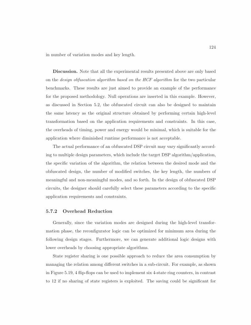
124
in number of variation modes and key length.
Discussion. Note that all the experimental results presented above are only based
on the design obfuscation algorithm based on the HCF algorithm for the two particular
benchmarks. These results are just aimed to provide an example of the performance
for the proposed methodology. Null operations are inserted in this example. However,
as discussed in Section 5.2, the obfuscated circuit can also be designed to maintain
the same latency as the original structure obtained by performing certain high-level
transformation based on the application requirements and constraints. In this case,
the overheads of timing, power and energy would be minimal, which is suitable for the
application where diminished runtime performance is not acceptable.
The actual performance of an obfuscated DSP circuit may vary significantly accord-
ing to multiple design parameters, which include the target DSP algorithm/application,
the specific variation of the algorithm, the relation between the desired mode and the
obfuscated design, the number of modified switches, the key length, the numbers of
meaningful and non-meaningful modes, and so forth. In the design of obfuscated DSP
circuits, the designer should carefully select these parameters according to the specific
application requirements and constraints.
5.7.2 Overhead Reduction
Generally, since the variation modes are designed during the high-level transfor-
mation phase, the reconfigurator logic can be optimized for minimum area during the
following design stages. Furthermore, we can generate additional logic designs with
lower overheads by choosing appropriate algorithms.
State register sharing is one possible approach to reduce the area consumption by
managing the relation among different switches in a sub-circuit. For example, as shown
in Figure 5.19, 4 flip-flops can be used to implement six 4-state ring counters, in contrast
to 12 if no sharing of state registers is exploited. The saving could be significant for

125
a large circuit. In Figure 5.19, the registers marked in bold represent the active state
registers for corresponding ring counters.
S0 S1 S2 S3R3 R1 R0
S1 S3 S0 S2R3 R2 R0
S3 S2 S1 S0R3 R2 R1 R0
S2 S0 S3 S1R2 R1 R0
S1 S0 S2 S3R2 R0
S1 S3 S2 S0R3 R1 R0
msb
R3 R2 R1 R0
Clock 0
Clock 1
Clock 2
Clock 3
0 0 1 1
0 1 0 1
1 1 0 0
1 0 1 0
R3 R1
R2
R1
R3
R2
Figure 5.19: State registers sharing.
Furthermore, exploiting the relation among the state registers is more effective than
managing the output function or the next-state function to control the relations among
different switches in a sub-circuit. However, note that by using these design optimization
techniques, the structural obfuscation degree (SOD) will be degraded, as the number of
independent switches (Ns) is decreased.
5.8 Comparison to existing obfuscation methods
As our work is the first attempt to develop a methodology to obfuscate DSP cir-
cuits by utilizing high-level transformations, it is hard to compare with other existing
obfuscation methods which are general to a wide variety of designs. Therefore, we have
introduced two metrics to analyze the security, which are discussed in Section 5.6.

126
Most of the hardware obfuscation techniques in the literature can also be applied to
DSP circuits. However, the use of high-level transformations from a security perspec-
tive has not been incorporated into any of these prior hardware obfuscation techniques.
Moreover, other circuit locking techniques only achieve protection at one-level (i.e., en-
crypt the normal functionality by a key), while our proposed methodology provides a
two-level protection (i.e., structural obfuscation and functional obfuscation). The main
advantage of the proposed methodology is the generation of meaningful variation modes
from a signal processing point of view, since the meaningful modes create ambiguity to
the adversary such that it is hard for the adversary to distinguish the desired func-
tionality from other variation modes. Other existing methods, such as [62, 61], are not
specific to DSP circuits, which would not be able to ensure meaningful variation modes
from a signal processing point of view. Moreover, meaningful variation modes enable
our proposed design methodology to be adaptable to reconfigurable applications.
Finally, when considering the metrics of the design performance, our proposed
methodology is also superior. While our proposed approach only alters the logic of
switches, most of the existing methods are based on explicit FSM modifications (e.g.,
the technique proposed in [45]), which are not scalable since the construction of the
FSM is not practical for even moderate-sized circuits, not to mention that the number
of added obfuscation states can be relatively large as compared to the original FSM. In
our proposed methodology, area consumption is slightly increased due to the increased
cost of the control logic for the obfuscated switches.
5.9 Conclusion and Future Work
This chapter presents a novel low-overhead solution to design DSP circuits that
are obfuscated both structurally and functionally by utilizing high-level transformation
techniques. It is shown that verifying the equivalence of digital signal processing cir-
cuits by employing high-level transformations will be harder if some switches can be

127
designed in such a way that are difficult to trace. A secure reconfigurable switch design
is incorporated into the proposed design scheme to improve the security. A complete
design flow is presented. In the proposed obfuscation methodology, the variation modes
and the additional obfuscating circuits could also be designed systematically based on
the high-level transformations. Compared to other existing obfuscation methods, an-
other advantage of the proposed methodology is the generation of meaningful variation
modes from a signal processing point of view, since the meaningful modes create ambi-
guity to the adversary such that it is hard for the adversary to distinguish the correct
functionality from other variation modes. Experimental results have demonstrated the
effectiveness of the proposed methodology.

Chapter 6
Beat Frequency Detector based
True Random Number
Generators: Statistical Modeling
and Analysis
6.1 Introduction
The security of most cryptographic systems relies on unpredictability and irrepro-
ducibility of digital key-streams that are used for encryption and/or signing of confi-
dential information. These key-streams are generated by random number generators
(RNG), which can be further classified into two categories: true random number gen-
erators (TRNG) and pseudo random number generators (PRNG). The key difference
between TRNG and PRNG lies in the entropy source component. A TRNG derives ran-
domness from an analog physical process (electronic thermal noise, radioactive decay,
etc.), while a PRNG relies on computational complexity, whose outputs are completely
determined by the seed. TRNGs are used for authentication and encryption purposes
128

129
in systems requiring a high level of security. On-chip TRNGs typically harvest random-
ness from a circuit that converts transistor level noise such as random telegraph noise
(RTN), flicker noise and thermal noise [81, 82, 83, 84, 85, 86, 87] into a voltage or delay
signal.
A source of randomness commonly used in FPGA and ASIC implementations of
TRNGs is the unpredictability of signal propagation time across logic gates. This un-
predictability is typically accumulated in so-called ring oscillators (ROSCs), consisting
of a series of inverters or delay elements connected in a ring. The phase jitter of a
ring oscillator is then extracted by another ring oscillator or by an external clock signal.
Ring oscillators and the underlying physical phenomena have been widely studied in the
literature as building blocks for many on-chip TRNGs [88, 89, 90, 91, 92, 93, 94, 95].
One major advantage of these TRNG designs is that no analog component is required,
while conventional delay based TRNGs typically involve extensive analog components
for amplifying the device noise [96], which makes them less suitable for practical TRNG
devices.
Evaluating TRNGs is a difficult task. Clearly, it should not be limited to testing the
TRNG output bitstream. The physical characteristics of the source of randomness and
the randomness extraction method determine the principal parameters of the generated
bit stream: the bias of the output bit stream, correlation between subsequent bits,
visible patterns, etc. While some of the non-randomness can be corrected by efficient
post-processing, it is better if the generator inherently produces a good quality random
bitstream. Furthermore, passing NIST [97] or DIEHARD [98] tests does not guarantee
a TRNG, as these tests were originally designed to check the performance of PRNGs.
One important requirement in TRNG security evaluation is the existence of a math-
ematical model of the physical noise source and the statistical properties of the digitized
noise derived from it [99]. If a stochastic model of the physical randomness source is
available, it can be used in combination with the raw signal to estimate the entropy and
the bias depending on the random input variables and the TRNG principle. Therefore,

130
in order to provide a proof of security for a TRNG, an analysis of the statistical property
of the underlying mathematical model is needed. However, creating a model of a TRNG
is difficult as the model parameters are unknown. Thus, it is impossible to predict per-
formance of new TRNG designs as their models cannot be created. On the other hand,
it can be argued that TRNG performance can only be measured from fabricated chips.
Therefore, how good a new TRNG design can only be determined by measurements
from a fabricated design. This chapter exploits the synergy between a model and the
measurements of the real device. A new ROSC based BFD-TRNG was fabricated and
tested [100]. Based on NIST tests, this TRNG was demonstrated to be an effective
TRNG. Our work, for the first time, presents a model of this BFD-TRNG. The model
parameters are derived by fitting the data measured from the fabricated device. Based
on this created model, a rigorous analysis of the BFD-TRNG is presented. Further-
more, several new BFD-TRNG architectures are proposed and their performances are
predicted based on the proposed model.
6.2 Beat Frequency Detector based TRNG
The oscillator sampling method extracts randomness from phase noise in free-running
oscillators [88, 89, 92]. An example of this technique is shown in Figure 6.1, where the
output of a fast oscillator is sampled on the rising edge of a slower ring oscillator us-
ing a D flip-flop (DFF). Note that the design parameters for the inverters of the two
ROSCs are not necessarily the same. The timing fluctuations of the edges of the slow
signal relative to the fast oscillator is the source of the randomness in the ROSC based
TRNG. Oscillator jitter causes uncertainty in the exact sample values, ideally producing
a random bit for each sample. Additionally, randomness can be artificially enhanced by
carefully selecting the ratio of the fast and slow oscillator frequencies. Periods of these
oscillations vary from cycle to cycle causing jitter in the rising and falling edges. The
goal is to sample the signal at a point in time that is in close proximity of a transition

131
zone thereby making sampled value unpredictable. In order to accumulate sufficient jit-
ter when the fast ring oscillator is sampled, a large ratio of the fast and slow oscillator
frequencies is usually desired. Note that the slow oscillator can also be substituted by
an external clock, such as in the IBM M -parallel structure [101].
DFFD Q
B
A
Figure 6.1: Two-oscillator TRNG.
Built on the prior work of ROSC based TRNGs, we have proposed a novel TRNG
design to harvest randomness from jitter variation based on the beat frequency detector
(BFD) [100]. A beat frequency detector captures the frequency difference between the
two ROSCs [102] with a very high resolution, which was originally used to measure
frequency degradation of digital circuits. As shown in Figure 6.2, the ROSC A is
continuously sampled by a ROSC B whose frequency is slightly different from ROSC
A. The output of the DFF exhibits the beat frequency Δf , which is determined by
the frequency difference of the two ROSCs. A counter measures the beat frequency
with ROSC B as the clock. The counter output increments every ROSC period until
it reaches the beat frequency interval after which the count is sampled and reset. The
mean of the frequency difference of the two ROSCs is caused by manufacturing process
variations, and can be further adjusted by trimming capacitors associated with the ring
oscillators [100]. The output count will fluctuate due to the random jitter in the circuit.
Under the presented setting, we can generate approximately 3.25 bits per sample by
using first 3 least significant bits (LSBs) directly and processing the 4th LSB with the
von Neumann corrector [103].

132
DFF
Cou
nter
Res
etD Q
B
A C
fA
fB
AB
C
N
N
(a) (b)
ROSC A
ROSC BBFD &
CounterScan out
52μm
96μm
124μm
DCAP
DCAP
Figure 6.2: BFD-TRNG: (a) basic principle, (b) die microphotograph in 65nm.
Overall, there are a number of circuit level advantages of the BFD-TRNG compared
to other existing ROSC based TRNGs [100]:
1. Higher tolerance to temperature or voltage drifts.
2. Fully digital operation.
3. Increased number of random bits per sample.
4. Reduced sampling time.
5. Minimal calibration, i.e., one-time calibration of the average count during start
up is needed.
6.3 Physical Component Modeling of RO TRNGs
As discussed above, the statistical tests such as NIST and DIEHARD are designed to
check the performance of PRNGs. The core of a TRNG is its randomness source, which
usually generates a time-continuous analog signal that is digitized by certain harvest
mechanism. In order to validate a TRNG, characterization of the randomness source

133
and the harvest mechanism are needed. In this section, we investigate the statistical
properties of the BFD-TRNG.
The randomness source of the ring oscillator based TRNGs is the timing jitter in
each ROSC, which is a stochastic phenomenon caused by internal random noise such
as thermal, shot, and random telegraph noise in the transistors of a ring oscillator.
Jitter can be considered as a short-term variation of a digital signal from their ideal
position in time. The size of the jitter is determined by the properties of the hardware
device and the operating environment. In these ROSC based TRNG designs, two or
more oscillators are combined to produce a random bitstream. This jitter will create an
accumulated phase drift in each ring so that the transition region in the sampling period
is assumed to be unpredictable. In the literature, several studies of the jitter in ring
oscillators have been presented [104, 105, 106, 107, 108, 109, 110]. More precisely, the
jitter model should incorporate a Gaussian variable, 1/f noise, and a coupling sinusoidal
signals [89]. However, existing works [105, 106] report that the durations between the
transition times appear in many cases to be independent and identically distributed
Gaussian, as it is the most dominant component. This allows us to create simple model
for ROSC based TRNGs by characterizing the jitter as a Gaussian random variable with
zero mean. Moreover, there are two major reasons that we do not consider Random
Telegraph Noise (RTN) as the major random noise source: First, due to the averaging
effect, the RTN induced jitter is much smaller than that on a single transistor. Second,
the occurrence of RTN with large amplitude and high frequency is rare [81, 111].
A ROSC consists of an odd number of inverters connected together in a ring configu-
ration. This causes the output of the oscillator to change with a period of approximately
2kD, where k is the number of inverters in a ROSC andD is the delay of a single inverter.
If we consider the delay of each inverter as a Gaussian random variable Di ∼ N(μi, σ2i ),
a period of the ROSC can be written as
T = 2k∑
i=1
Di ∼ N(μ, σ2), (6.1)

134
which is also a Gaussian random variable. For simplicity, we directly consider a period
of the ROSC as a Gaussian random variable in this chapter. Periods vary from cycle
to cycle causing jitter in the rising and falling edges. Note that this model can incor-
porate different operating conditions (e.g., temperature, supply voltage) by modifying
σ accordingly.
6.4 Statistical Analysis of BFD-TRNG
Based on the illustrated model above, this section presents a comprehensive statis-
tical analysis to help resolve some important BFD-TRNG design issues:
(a) How much of the frequency difference is required to produce sufficient random
numbers?
(b) How many bits of the counter value can be used?
(c) How can the TRNG performance be further improved?
6.4.1 BFD Model
As shown in Figure 6.2, the BFD-TRNG consists of two ROSCs whose frequencies
are slightly different. The period of the two ROSCs can be modeled as TA ∼ N(μA, σ2A)
and TB ∼ N(μB, σ2B), respectively. Note that the two ring oscillators are implemented
identical, therefore their free-running frequencies are very close but not identical due to
the process variation. To prevent injection locking phenomenon or any other unintended
coupling between the two ROSCs, we separated the frequencies of the two ROSCs
using trimming capacitors prior to the testing. Experimental data showed no signs
of correlation between the ROSC frequencies [100]. An output will be generated once
the beat frequency is obtained, i.e., the faster ROSC completes one more cycle than
the slower ROSC. The output will be the number of cycles completed by ROSC B at
this moment. Without loss of generality, we always assume ROSC A is faster than

135
ROSC B in this chapter, i.e., μA < μB. Since the inverters in ROSC A and ROSC
B are almost equivalently designed with only slight frequency difference and operated
under the same environmental condition, we can assume σ = σA = σB. Therefore, the
probability density function (pdf) of the counter value N can be expressed as
pdf(N) = {min N :N∑i=1
TAi <
N−1∑i=1
TBi} = {min N : TAN <
N−1∑i=1
(TBi − TAi)}. (6.2)
However, the N in Equation (6.2) does not have a standard probability density function.
Instead, we perform Monte Carlo simulations to study the statistical properties of this
model. Model parameters extracted from experimental measurements in [100] imply
ΔμμB
= μB−μAμB
= 0.28% and σA = σB = 0.0006. Note that in this chapter, without loss
of generality, we always assume the mean of the clock signal of the DFF to be 1 (i.e.,
μB = 1). Therefore, Δμ = 0.0028 and μA = 0.9972 in this setup. The distribution of
the counter values is shown in Figure 6.3.
330 340 350 360 370 380 3900
1000
2000
3000
4000
5000
6000
7000
8000
Counter Value
Figure 6.3: Counter value distribution (Δμ = 0.28%, σ = 0.0006).
6.4.2 Effect of Counter Value
Mean of Counter Value
It can be seen from Figure 6.3 that the mean of the counter values is close to
1Δμ = 357. We repeat the simulation with Δμ = 0.4% as shown in Figure 6.4. The
mean is also close to 1Δμ = 250. Thus, we observe that the mean of counter values is
inversely proportional to the value of Δμ.

136
235 240 245 250 255 260 2650
2000
4000
6000
8000
10000
12000
14000
Counter Value
Figure 6.4: Counter value distribution (Δμ = 0.4%, σ = 0.0006).
This property can also be derived by mathematically. Since Equation (6.2) does
not have a closed-form expression, we consider a simpler case: TA and TB remain
unchanged during one measurement time. In fact, this is the original function of a beat
frequency detector, i.e., to measure the frequency difference of ROSC A and ROSC B.
In this case, Equation (6.2) can be simplified to
N = {min N : |N − NTB
TA| ≥ 1}. (6.3)
By solving the equation, we can get
N = � TB
|TB − TA| �. (6.4)
There is one trivial observation that |TB − TA| cannot be very small; otherwise,
the counter value will be very large (i.e., only one counter value can be obtained in very
large number of cycles). If we consider TA and TB as the average periods of N cycles,
these can be characterized as Gaussian random variables∑N
i=1 TAi
N ∼ N(1−Δμ, σ2
N ) and∑N
i=1 TBi
N ∼ N(1, σ2
N ), respectively. Thus,
TB
TB − TA∼ N(1, σ
2
N )
N(Δμ, 2σ2
N ), (6.5)

137
which can be described as a ratio of two Gaussian random variables. We can approxi-
mate the expected value of TBTB−TA by a second order Taylor expansion [112]:
E(TB
TB − TA) ≈ E(TB)
E(TB − TA)− Cov(TB, TB − TA)
E2(TB − TA)+
V ar(TB − TA)E(TB)
E3(TB − TA)
=1
Δμ−
σ2
N
Δμ2+
2σ2
N
Δμ3
=1
Δμ+
1
N
σ2
Δμ2(2
Δμ− 1). (6.6)
Based on the assumption that TA and TB are uncorrelated, we can obtain that
Cov(TB, TB − TA) = V ar(TB) = σ2. For the parameters Δμ = 0.28%, σ = 0.0006,
the above equation will equal to
1
Δμ+
1
N
σ2
Δμ2(2
Δμ− 1) = 357.14 +
32.75
N. (6.7)
It can be seen from Figure 6.3 that 330 < N < 390. Consequently, the second term
of Equation (6.7) (i.e., 32.75N ) is less than 0.1. Consequently, the mean of counter values
is approximately 1Δμ ≈ 357 in this case.
Typically, the second term of Equation (6.7) will be relatively small compared to
1Δμ , since Δμ is a very small number and σ2
Δμ2 is generally less than 1.
As a result, we can conclude
E(N) ≈ 1
Δμ. (6.8)
Thus, in contrast to the original function of the BFD, i.e., to measure the slight
frequency difference of two signals, we should set up an appropriate frequency difference
for the two ROSCs. In other words, trimming capacitors should be used to set an
appropriate Δμ for the two ROSCs, instead of equalizing their frequencies or making
the frequency differences as small as possible. Therefore, we mainly harvest randomness
from the jitter noise instead of the metastability in our design, as the random numbers
are generated from the delay difference variations of the two ROSCs, instead of from
sampling one ROSC with another ROSC. Note that our current test chips provide a

138
frequency trimming resolution of 0.1%, this can be further reduced with more trimming
capacitor bank controls.
Dynamic Range of Counter Value
The randomness of the BFD-TRNG comes from the counter values. If the dynam-
ic range is larger, we could use more bits of the counter value as random numbers.
Therefore, it is important to examine the statistics of the dynamic range of the counter
values. We attempt to use a Gaussian distribution to fit the counter values from ex-
perimental measurements and consider 6σG as the dynamic range based on the fitting
result N(μG, σ2G). An example is shown in Figure 6.3, with parameters Δμ = 0.28%,
σ = 0.0006. It is shown that the distribution of the counter values is close to a Gaussian
distribution. In this case, the dynamic range 6σG is equal to 34.6.
We repeat the simulation for different parameters as shown in Figure 6.4 and Fig-
ure 6.5, whose dynamic ranges are 20.3 and 68.9, respectively. The relationship between
the dynamic range of counter values and Δμ is shown in Figure 6.6, where the mean of
counter values is equal to 1Δμ . It can be seen that the dynamic range of counter values
will increase with the increase of σ, while it will decrease with the increase of Δμ. This
observation is also conformed from our measured chip data [100]. Moreover, it can be
seen that only slight change of Δμ will affect the counter values significantly.
300 320 340 360 380 400 4200
500
1000
1500
2000
2500
3000
3500
4000
Counter Value
Figure 6.5: Counter value distribution (Δμ = 0.28%, σ = 0.0012).

139
100 200 300 400 500 600 700 800 900 10000
20
40
60
80
100
120
140
160
180
Mean (Counter Value)
Dyn
amic
Ran
ge (C
ount
er V
alue
)
Figure 6.6: The relationship between the dynamic range of counter values and Δμ (σ =0.0006%).
0 0.5 1 1.5 2 2.5 3x 10⁻³
020406080
100120140160180200
sigma
Dyn
amic
Ran
ge (C
ount
er V
alue
)
Figure 6.7: The relationship between the dynamic range of counter values and σ (Δμ = 0.28%).

140
We can also examine the variance of counter values by a second order Taylor expan-
sion [112]:
V ar(TB
TB − TA) ≈ E2(TB)
E2(TB − TA)(V ar(TB)
E2(TB)− 2
Cov(TB, TB − TA)
E(TB)E(TB − TA)+
2V ar(TB − TA)
E2(TB − TA))
=1
Δμ2(σ2
N− 2σ2
NΔμ+
2σ2
NΔμ2)
=σ2
NΔμ2(1− 2
Δμ+
2
Δμ2). (6.9)
Since we have demonstrated that the expected value of N is approximately 1Δμ and
Δμ is a very small value, we can further approximate the above equation as
V ar(TB
TB − TA) ≈ σ2
NΔμ2(1− 2
Δμ+
2
Δμ2)
≈ σ2
Δμ
(2(
1
Δμ− 1
2)2 +
1
2
)
≈ 2σ2
Δμ3. (6.10)
Consequently, we can obtain
σG ≈√
V ar(TB
TB − TA) ≈
√2σ
Δμ32
. (6.11)
Thus, we can conclude that the dynamic range of counter values increases linearly
with σ and is inversely proportional to Δμ32 .
6.4.3 Bounds on Bias of Each Bit
According to the NIST test, the probability of ”1” occurrence, p1, should satisfy
49.91% ≤ p1 ≤ 50.09% to pass the frequency test of NIST tests [97]. For any bit of
the counter values, if the probability of ”1” occurrence is within the acceptance range
[49.91%, 50.09%], then this bit might be used as random numbers directly. Otherwise,
certain techniques are required to post-process the bit. Note that we only consider the
biasedness metric in our simulation, as other metrics are completely dependent on the
performance of the employed pseudo random number generator for simulation. The p1

141
of each bit for the distribution in Figure 6.3 is presented in the second row of Table 6.1.
Since the counter values are less than 512 in our setup, we only need to consider the
first 9 LSBs. It can be seen that the first 3 LSBs are within the acceptance range. In
fact, our chip experimental results show that all of the first 3 LSBs can pass the NIST
test individually or collectively after serializing them.
Table 6.1: The Probability of ”1” Occurrence p1 for Each BitDistribution p1(b8) p1(b7) p1(b6) p1(b5) p1(b4) p1(b3) p1(b2) p1(b1) p1(b0)Figure 6.3 1 0 1 0.8384 0.1979 0.4564 0.5003 0.4991 0.4995Figure 6.8 0.5173 0.4827 0.4827 0.4827 0.4838 0.4991 0.4998 0.5007 0.5005
We also present the value of p1 of each bit for the distribution as shown in Figure 6.8
with parameters Δμ = 0.391% and σ = 0.0009 in Table 6.1. The dynamic range 6σG is
30.2 which is less than the dynamic range of the distribution in Figure 6.3. However,
the first 4 LSBs are within the acceptance range. Furthermore, the higher bits are
also less biased compared to counter values in Figure 6.3. Therefore, the counter values
in Figure 6.8 have better randomness than the counter values in Figure 6.3, even though
the dynamic range of the counter values in Figure 6.8 is smaller.
230 235 240 245 250 255 260 265 270 275 2800
1000
2000
3000
4000
5000
6000
7000
8000
Counter Value
Figure 6.8: Counter value distribution (Δμ = 0.391% and σ = 0.0009).
As a result, we can conclude that the number of bits that we can use is not only
dependent on the dynamic range, but also dependent on the mean of the counter values.
For example, we consider the two cases as shown in Figure 6.9. The counter values in
the top and the bottom panels of Figure 6.9 have the same dynamic range. However,

142
the mean of counter values in the top panel is 15.5, which is just at the boundary of
b3 = 0 and b3 = 1. As a result, the expected bias ε will be 0, where ε is defined as
ε = |0.5−p1|. For the counter values in the bottom panel whose mean is 19.5, p1 = 0.11.
Thus, the bias is |0.5− p1| = 0.39. This is because the mean of the counter values is in
the middle of the region where b3 = 0.
b3 0 1 0 1 0
0 5 10 15 20 25 30 35 400
0.1
0.2
Counter Value
Dis
tribu
tion
0 5 10 15 20 25 30 35 400
0.1
0.2
Counter Value
Dis
tribu
tion
Figure 6.9: The biasedness of b3 for different counter values.
For a certain dynamic range of counter values, in the best case, E(N) = 2km−0.5 for
bk (m is an integer), which leads to ε = 0. In the worst case, E(N) = 2km+2k−1− 0.5,
which generates the largest bias ε. Ideally, we can extract more randomness from the
counter values by carefully adjusting the mean. However, in order to ensure the quality
of each bit when taking noise and operating environmental change into consideration,
we have to consider the bias in the worst case. Table 6.2 presents the corresponding
bias ε for each bit under different σG in the worst case.
It can be seen from Table 6.2 that the first LSB is guaranteed to be unbiased if
the dynamic range of counter values is greater than 6σG = 12. Furthermore, if the
dynamic range is greater than 30, the first 3 LSBs might be used as random numbers
without any post-processing. As a result, we have to ensure at least a dynamic range
of 30 for the BFD-TRNG [100], if we output the first 3 LSBs directly. In addition, we

143
Table 6.2: Bias ε for Each Bit under Different σG in the Worst CaseσG ε(b8) ε(b7) ε(b6) ε(b5) ε(b4) ε(b3) ε(b2) ε(b1) ε(b0)1 0.5 0.5 0.5 0.5 0.5 0.4999 0.4545 0.1854 0.00462 0.5 0.5 0.5 0.5 0.4999 0.4545 0.1854 0.0046 03 0.5 0.5 0.5 0.5 0.4923 0.3176 0.0397 0 04 0.5 0.5 0.5 0.4999 0.4545 0.1854 0.0046 0 05 0.5 0.5 0.5 0.4986 0.3904 0.0926 0.0003 0 06 0.5 0.5 0.5 0.4923 0.3176 0.0397 0 0 07 0.5 0.5 0.5 0.4777 0.2475 0.0146 0 0 08 0.5 0.5 0.4999 0.4545 0.1854 0.0046 0 0 09 0.5 0.5 0.4996 0.4246 0.1336 0.0012 0 0 010 0.5 0.5 0.4986 0.3904 0.0926 0.0003 0 0 011 0.5 0.5 0.4964 0.3542 0.0618 0.0001 0 0 012 0.5 0.5 0.4923 0.3176 0.0397 0 0 0 013 0.5 0.5 0.4862 0.2816 0.0245 0 0 0 014 0.5 0.4999 0.4777 0.2475 0.0146 0 0 0 015 0.5 0.4999 0.4671 0.2153 0.0083 0 0 0 0
cannot use b4 to b8 directly while the dynamic range is less than 90. Since the dynamic
range increases with the increase of the mean of the counter values, we have to set an
appropriate Δμ to attain sufficient randomness of the TRNG design.
Figure 6.10 shows the relationship between the number of bits that we can output
directly and the dynamic range. The number of unbiased bits can be expressed by
fitting the curve perfectly as
number of unbiased bits = log2 4023
+ log2σG� = log2 4023
+ log2σ − 3
2log2Δμ+
1
2�.
(6.12)
Therefore, we can conclude that the number of bits that we can use is logarithmically
proportional to the dynamic range of the counter values.
Summary
The observations are summarized below.
1. The mean of the counter values is inversely proportional to Δμ.
2. The dynamic range of counter values is inversely proportional to Δμ32 and is
proportional to σ.

144
0 5 10 15 20 25 3000.5
11.5
22.5
33.5
44.5
5
sigmaG
Num
ber o
f Unb
iase
d Bi
ts
Figure 6.10: The relation between the number of unbiased bits and the value of σG.
3. The sampling rate is inversely proportional to the mean of counter values.
4. The number of unbiased bits is logarithmically proportional to the dynamic range
of counter values; thus, it is inversely logarithmically proportional to Δμ32 .
5. The sampling rate is proportional to Δμ.
As we are only able to control the value of Δμ, we should set an appropriate Δμ
to achieve better throughput. Note that a higher σ can be obtained by appropriately
sizing the transistor and choosing number of stage in the ROSCs, but this is out of
the scope of this chapter. For post-fabrication throughput optimization, we are able to
achieve better throughput with the following two methods based on Δμ controlling.
(a) Use a higher Δμ (i.e., lower counter values), which could improve the sampling
rate. But we may only be able to use limited number of bits from each counter
value as random numbers.
(b) Use a lower Δμ (i.e., higher counter values). The sampling rate is reduced. But
we can use more bits from the counter values as random numbers. Moreover, we
can further post-process the higher bits of the counter values to generate more
bits.
Based on the summary above, we can obtain the relationship between the throughput
(i.e., rate × number of unbiased bits) of the BFD based design and parameters Δμ, σ

145
as below:
throughput ∝ Δμ log2 4023
+ log2σG� ≈ Δμ log2 4023
+ log2σ − 3
2log2Δμ+
1
2�. (6.13)
If we consider Equation (6.13) without the floor function as
throughput ∝ Δμ(log240
23+ log2σ − 3
2log2Δμ+
1
2). (6.14)
Equation (6.14) achieves maximum value at
Δμ = 2(23log2
40√2σ
23− 1
ln2). (6.15)
For example, the values of Equations (6.13) and (6.14) are shown in Figure 6.11 when
σ = 0.0006.
100 200 300 400 500 600 700 800 900 10000
0.005
0.01
Mean (Counter Value)
Valu
e of
Equ
atio
n (1
3)
100 200 300 400 500 600 700 800 900 10000
0.005
0.01
Mean (Counter Value)
Valu
e of
Equ
atio
n (1
4)
Figure 6.11: Values of Equations (6.13) and (6.14) for different Δμ’s (σ = 0.0006).
It can be seen from the top panel of Figure 6.11 that the BFD-TRNG achieves the
best throughput when Δμ = 0.0050 (2 bits can be used as random numbers), while the
maximum value of Equation (6.14) is achieved at Δμ = 2(23log2
40√2σ
23− 1
ln2) = 0.004768 as
shown in the bottom panel. Therefore, in this case, we can adjust the Δμ such that
the mean of the counter values is about 200 to achieve higher throughput. Generally,
the Δμ should be adjusted according to the environmental noise σ based on Equation
(6.15).
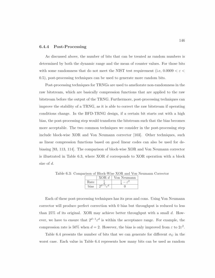
146
6.4.4 Post-Processing
As discussed above, the number of bits that can be treated as random numbers is
determined by both the dynamic range and the mean of counter values. For those bits
with some randomness that do not meet the NIST test requirement (i.e, 0.0009 < ε <
0.5), post-processing techniques can be used to generate more random bits.
Post-processing techniques for TRNGs are used to ameliorate non-randomness in the
raw bitstream, which are basically compression functions that are applied to the raw
bitstream before the output of the TRNG. Furthermore, post-processing techniques can
improve the stability of a TRNG, as it is able to correct the raw bitstream if operating
conditions change. In the BFD-TRNG design, if a certain bit starts out with a high
bias, the post-processing step would transform the bitstream such that the bias becomes
more acceptable. The two common techniques we consider in the post-processing step
include block-wise XOR and Von Neumann corrector [103]. Other techniques, such
as linear compression functions based on good linear codes can also be used for de-
biasing [93, 113, 114]. The comparison of block-wise XOR and Von Neumann corrector
is illustrated in Table 6.3, where XOR d corresponds to XOR operation with a block
size of d.
Table 6.3: Comparison of Block-Wise XOR and Von Neumann CorrectorXOR d Von Neumann
Rate 1d
14 − ε2
bias 2d−1εd 0
Each of these post-processing techniques has its pros and cons. Using Von Neumann
corrector will produce perfect correction with 0 bias but throughput is reduced to less
than 25% of its original. XOR may achieve better throughput with a small d. How-
ever, we have to ensure that 2d−1εd is within the acceptance range. For example, the
compression rate is 50% when d = 2. However, the bias is only improved from ε to 2ε2.
Table 6.4 presents the number of bits that we can generate for different σG in the
worst case. Each value in Table 6.4 represents how many bits can be used as random

147
numbers for a certain counter value. For example, if a bit has a bias ε < 0.0009, the
bit can produce 1 random bit per sample. However, if the bias ε exceeds the threshold,
this bit of the counter value can be used to generate 1d random bit per sample by using
block-wise XOR or 14 − ε2 bit per sample by the Von Neumann corrector. Entropy
is essentially an upper bound on the number of bits that we can generate for a given
dynamic range. Note that the total entropy can be obtained by the sum of the entropy
for each individual bit, according to Table 6.2.
Table 6.4: Number of Bits per Sample for Different σG in the Worst CaseσG Von Neumann XOR Entropy1 0.51 0.64 2.172 1.51 1.64 3.173 2.41 2.4 3.754 2.51 2.64 4.175 3.34 3.29 4.496 3.41 3.4 4.757 3.46 3.61 4.978 3.51 3.64 5.179 3.55 3.7 5.3410 4.34 4.29 5.4911 4.37 4.3 5.6212 4.41 4.4 5.7513 4.43 4.42 5.8614 4.46 4.61 5.9715 4.49 4.63 6.07
It can be seen that the block-wise XOR and Von Neumann corrector have comparable
performances for the BFD-TRNG. However, for the bit with a small bias, XOR will be
more favored than Von Neumann corrector. As we always try to utilize the bits with
smaller biases, block-wise XOR could outperform Von Neumann corrector in general.
From the simulation results, besides the bits of counter values that we can output
directly, we may only be able to use 2 more bits by post-processing, as the rate will
be too low for the higher bits. According to Table 6.2, for example, we can use the
first 3 LSBs directly when σG = 7. If we only want to post-process the 4th LSB to
generate more bits, we can generate 3.5 bits per sample by XOR or approximately 3.25

148
bits per sample by Von Neumann corrector. Moreover, the output of block-wise XOR is
synchronous while the output of Von Neumann corrector is asynchronous. The challenge
of using block-wise XOR is that we need to determine the value of d for each bit based
on the dynamic range of the counter values.
6.4.5 Online Test and Feedback Control
Due to tolerances of the components, aging effects, a total breakdown of the noise
source or possible active attacks, the TRNG may output considerably weaker random
numbers. Online tests can be very useful for a TRNG to detect non-tolerable weaknesses
while the TRNG is in operation [115]. Based on our statistical analysis results, the
counter values can be easily used as a performance indicator. We can monitor the
counter values during operation. Note that we will monitor higher bits of the counter
value to achieve feedback control, while LSBs are used as random numbers. As a result,
the problem of output manipulation can be avoided. If the dynamic range or mean of
the counter values changes significantly, there is a high possibility of attack or significant
operating environmental change. In this case, TRNG should stop outputting random
numbers.
Furthermore, feedback control can be used to neutralize the environmental change
or aging effects. Trimming capacitors in ring oscillators can be adjusted adaptively to
keep the same value of Δμ based on our statistical analysis results. For example, we
can adjust the trimming capacitor according to the higher bits of the counter values,
while the lower bits are considered as random numbers.
Feedback control can also improve the efficiency of the BFD-TRNG:
(a) Based on the optimal relationship of Δμ and environmental noise σ as expressed
in Equation (6.15), we may adjust the trimming capacitor according to the distri-
bution of counter values during setup. For example, we can estimate the σ after
collecting a number of counter value samples based on Equation (6.11). Then

149
we will be able to determine whether the current Δμ is desired or it needs to be
adjusted.
(b) According to the dynamic range, the TRNG can decide the number of unbiased
bits that can be output directly in the worst case. Moreover, the type of post-
processing techniques can also be determined to extract random numbers from
higher bits of the counter values.
6.5 Alternate BFD-TRNG Architectures
Motivated by the statistical analysis results, in this section, we propose a number
of alternate BFD-TRNG designs, which can further improve the performances.
6.5.1 Parallel Structure
Parallelizability is also a desired metric of a TRNG. In fact, the BFD-TRNG is
notably easy to parallelize by adding as many extra ROSCs instead of 2 ROSCs to
generate multiple outputs, as shown in Figure 6.12. Our experimental results show
that the counter values of the two adjacent outputs are highly correlated. However,
the advantage of the BFD-TRNG is that we can consider bits of the counter values
individually. For example, the simulated correlation coefficients for a 4-parallel structure
are presented in Table 6.5. Note that the Δμ is assumed to be same for all the ROSC
pairs. According to NIST test, only the bitstreams with correlation coefficients less than
0.073 can pass the test [97]. It can be seen that the correlation coefficients of the counter
values of two adjacent outputs are large, i.e., around 0.5. However, the correlations of
the first 4 LSBs from two adjacent outputs are very small, while the counter values
and individual bits are not correlated for non-adjacent outputs. Therefore, it can be
concluded that the first 4 LSBs from the outputs in Figure 6.12 can still be used as
random numbers. In general, we can generate 3.25M bits per sample by using M + 1

150
ROSCs and M DFFs, since we can use the first 3 LSBs directly and generate 14 bits per
count by postprocessing the 4th LSB with Von Neumann corrector.
ROSC 1
ROSC 2
Output 1
ROSC 3
Output 2
ROSC M
ROSC M+1
Output M
......
......
DFFBeat
Frequency Counter
DFFBeat
Frequency Counter
DFFBeat
Frequency Counter
Figure 6.12: An M-parallel TRNG structure.
Table 6.5: Correlation Coefficients of Each Bit among the Outputs for a 4-Parallel StructureCorrelation Coefficients
Output (1,2) Output (2,3) Output (3,4) Output (1,3) Output (2,4) Output (1,4)
[b8 : b0] 0.4967 0.4970 0.4974 0.0018 -0.0006 -0.0007
b0 0.0005 0.0005 0.0008 -0.0003 0.0000 0.0009
b1 0.0003 0.0008 0.0016 -0.0006 -0.0004 -0.0018
b2 0.0010 0.0013 0.0005 0.0004 0.0001 -0.0016
b3 0.0027 0.0049 0.0023 0.0014 -0.0006 -0.0004
b4 0.1193 0.1177 0.1190 -0.0008 -0.0009 0.0002
b5 0.2974 0.2966 0.2971 0.0006 -0.0013 0.0001
b6 0.3023 0.2998 0.3001 0.0009 -0.0010 0.0001
b7 0.3023 0.2998 0.3001 0.0009 -0.0010 0.0001
b8 0.3023 0.2998 0.3001 0.0009 -0.0010 0.0001
6.5.2 Cascade Structure
A novel cascade structure which could achieve better randomness is shown in Fig-
ure 6.13. Note that ROSC B also connects to the clock signal of the counter (not shown
in Figure 6.13). The dynamic range of this cascade structure is higher than that of
the original BFD-TRNG. Figure 6.14 shows the counter value distributions of the orig-
inal BFD-TRNG and the cascade structure. Note that in our simulation, we set the
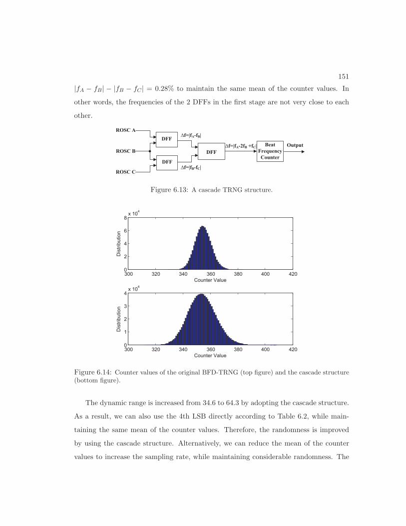
151
|fA − fB| − |fB − fC | = 0.28% to maintain the same mean of the counter values. In
other words, the frequencies of the 2 DFFs in the first stage are not very close to each
other.
DFF
DFF
DFF
ROSC A
ROSC B
ROSC C
Beat Frequency
Counter
Output
∆f=|fA-fB|
∆f=|fB-fC|
∆f=|fA-2fB +fC|
Figure 6.13: A cascade TRNG structure.
300 320 340 360 380 400 4200
2
4
6
8x 10⁴
Counter Value
Dis
tribu
tion
300 320 340 360 380 400 4200
1
2
3
4x 10⁴
Counter Value
Dis
tribu
tion
Figure 6.14: Counter values of the original BFD-TRNG (top figure) and the cascade structure(bottom figure).
The dynamic range is increased from 34.6 to 64.3 by adopting the cascade structure.
As a result, we can also use the 4th LSB directly according to Table 6.2, while main-
taining the same mean of the counter values. Therefore, the randomness is improved
by using the cascade structure. Alternatively, we can reduce the mean of the counter
values to increase the sampling rate, while maintaining considerable randomness. The

152
cascade structure will be extremely useful when the environmental noise is small. The
BFD-TRNG may even be adaptively configured between 3 ROSCs and 2 ROSCs. For
example, if the noise is relatively small, we could use 3 ROSCs as shown in Figure 6.13
to increase the dynamic range of counter values; otherwise, we could use 2 ROSCs as
shown in Figure 6.12 to output 2 bitstreams of random numbers. Furthermore, this cas-
cade structure provides higher flexibility for adjusting trimming capacitors associated
with the ring oscillators.
6.5.3 Parallel-Cascade Structure
We can also parallelize the cascade structure, which leads to the so-called parallel-
cascade structure of the BFD-TRNG. For example, a 4-parallel-cascade structure is
shown in Figure 6.15. Two adjacent outputs share two ring oscillators, while the outputs
that are separated from one output share one ring oscillator. We also need to examine
the correlation coefficients of the outputs to ensure the bits that are used as random
numbers are not correlated. The simulated correlation coefficients for the counter values
and the individual bits among different outputs are presented in Table 6.6. Note that we
set all the Δf ’s in Figure 6.15 as 0.0028. It can be seen that the correlation coefficients
for the first 4 LSBs between any two of the outputs are still very small and satisfy the
NIST criteria. The correlations of the counter values and higher bits (i.e., b4 to b8)
between two adjacent outputs are large, while the correlation coefficients of the counter
values and higher bits between the outputs 1 and 3 or the outputs 2 and 4 are smaller
but still exceed the threshold (i.e., 0.0073). The outputs 1 and 4 are not correlated
for both the counter values and the individual bits, since they do not share any ring
oscillator. Therefore, an M -parallel cascade structure can generate 4M bits per sample
by using (M + 2) ROSCs and (2M + 1) DFFs. Note that in order to generate 4 bits
from each output, we need to ensure the frequencies are either descending or ascending
from the first ROSC to the last ROSC, as Δf = ||fA−fB|−|fB−fC || = |fA−2fB+fC |only if fA > fB > fC or fA < fB < fC . Otherwise, Δf will equal to |fA − fC |, which

153
leads to the same dynamic range as the original BFD-TRNG. As a result, only 3.25 bits
can be obtained from each output in this case. However, there is a problem when M
is large that the frequency difference between the first ROSC and the last ROSC will
be fairly large if we want to generate 4 bits from each output, which may exceed the
capability of the trimming capacitors. Therefore, the frequencies need not necessarily
be set as either descending or ascending from the first ROSC to the last ROSC, which
leads to a parallel-cascade structure where some of the outputs can generate 4 bits each
and the others can generate 3.25 bits each. The performance is still improved.
DFF
DFF
DFF
ROSC A
ROSC B
ROSC C
Beat Frequency Counter
∆f=|fA-2fB +fC|
DFF
DFF
DFF
ROSC D
ROSC E
ROSC F
Beat Frequency Counter
∆f=|fD-2fE +fF|
DFF
DFFBeat
Frequency Counter
∆f=|fB-2fC +fD|
DFFBeat
Frequency Counter
∆f=|fC-2fD +fE|
Output 1
Output 2
Output 3
Output 4
Figure 6.15: A 4-parallel-cascade structure.
Table 6.6: Correlation Coefficients of Each Bit among the Outputs for a 4-Parallel-CascadeStructure
Correlation CoefficientsOutput (1,2) Output (2,3) Output (3,4) Output (1,3) Output (2,4) Output (1,4)
[b8 : b0] 0.6640 0.6634 0.6650 0.1666 0.1664 -0.0027
b0 0.0002 -0.0004 -0.0003 0.0001 0.0008 0.0000
b1 -0.0009 0.0012 0.0005 -0.0014 0.0005 -0.0003
b2 -0.0007 0.0011 -0.0007 -0.0006 0.0010 -0.0002
b3 -0.0029 -0.0015 -0.0023 0.0005 0.0006 -0.0004
b4 0.0377 0.0382 0.0388 0.0197 0.0181 -0.0001
b5 0.3539 0.3534 0.3542 0.1032 0.1013 0.0009
b6 0.1771 0.1673 0.1701 0.0163 0.0189 -0.0015
b7 0.1817 0.1721 0.1760 0.0145 0.0177 -0.0011
b8 0.1817 0.1721 0.1760 0.0145 0.0177 -0.0011

154
6.6 Comparison with Other Existing ROSC based TRNGs
Furthermore, by adopting the proposed statistical model, we could also analyze
prior ring oscillator based TRNG designs. In this section, we present the performance
comparisons of the BFD-TRNG with other existing ring oscillator based TRNGs.
6.6.1 Two-Oscillator TRNG
The most comprehensive model of a two-oscillator TRNG is presented in [109]. In
this section, we analyze the two-oscillator TRNG as shown in Figure 6.1 based on our
simple model, i.e., assume a Gaussian random variable for the period of a ring oscillator.
As discussed in Section 6.2, the frequency ratio between the two ROSCs plays a very
important role in the randomness of the output. Experimental results have shown that
the randomness is the worst when the fast oscillator frequency is an integer multiple of
half the slow oscillator frequency [104]. In practice, the ratio is often carefully selected
to achieve better randomness [92].
However, even if the TRNG design was originally designed to operate at a suitable
oscillator frequency/sampling frequency ratio, a change in environmental conditions or
worse adversarial influences may shift the frequency ratio to a weak operating point. It
is claimed that the amount of accumulated jitter 6σacc should be at least six times as
large as the period of the fast oscillator to attain sufficient randomness [116]:
6σacc ≥ 6μA, (6.16)
where σ2acc ≈ σ2
B+Lσ2A, since the randomness is generated from the timing fluctuations of
the edges of the slow signal relative to the fast oscillator. Let L represent the number of
periods ROSC A is completed before it is sampled. If we assume the design parameters
for the inverters of the two ROSCs are the same, σ2B will equal Lσ2
A, since the two
ROSCs accumulated approximately with the same amount of jitter. Consequently, the
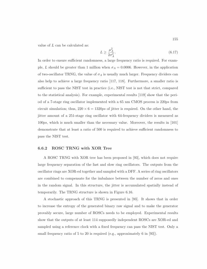
155
value of L can be calculated as:
L ≥ μ2A
2σ2A
. (6.17)
In order to ensure sufficient randomness, a large frequency ratio is required. For exam-
ple, L should be greater than 1 million when σA = 0.0006. However, in the application
of two-oscillator TRNG, the value of σA is usually much larger. Frequency dividers can
also help to achieve a large frequency ratio [117, 118]. Furthermore, a smaller ratio is
sufficient to pass the NIST test in practice (i.e., NIST test is not that strict, compared
to the statistical analysis). For example, experimental results [119] show that the peri-
od of a 7-stage ring oscillator implemented with a 65 nm CMOS process is 220ps from
circuit simulation; thus, 220× 6 = 1320ps of jitter is required. On the other hand, the
jitter amount of a 251-stage ring oscillator with 64-frequency dividers is measured as
100ps, which is much smaller than the necessary value. Moreover, the results in [101]
demonstrate that at least a ratio of 500 is required to achieve sufficient randomness to
pass the NIST test.
6.6.2 ROSC TRNG with XOR Tree
A ROSC TRNG with XOR tree has been proposed in [93], which does not require
large frequency separation of the fast and slow ring oscillators. The outputs from the
oscillator rings are XOR-ed together and sampled with a DFF. A series of ring oscillators
are combined to compensate for the imbalance between the number of zeros and ones
in the random signal. In this structure, the jitter is accumulated spatially instead of
temporarily. The TRNG structure is shown in Figure 6.16.
A stochastic approach of this TRNG is presented in [93]. It shows that in order
to increase the entropy of the generated binary raw signal and to make the generator
provably secure, large number of ROSCs needs to be employed. Experimental results
show that the outputs of at least 114 supposedly independent ROSCs are XOR-ed and
sampled using a reference clock with a fixed frequency can pass the NIST test. Only a
small frequency ratio of 5 to 20 is required (e.g., approximately 6 in [93]).

156
.
.
.DFF
D Q
Fs
.
.
.
Figure 6.16: ROSC TRNG with XOR tree.
However, some weakness of this TRNG design has been pointed out in [120]. The
main concern is that the XOR-tree and the sampling D flip-flop cannot handle the
high number of transitions from the oscillator rings. With many oscillator rings in
parallel, the number of transitions during a sampling period will be too high to meet
the setup/hold-time requirements. Experimental results show that approximately 50%
of the transitions get lost [121]. To cope with the problem with many transitions in the
sampling period, an enhanced TRNG based on the ROSCs has been proposed in [94] by
adding an extra DFF after each ring oscillator before the XOR gate Figure 6.17. This
TRNG design can generate desirable raw bitstream with a significantly reduced number
of ROSCs. Its outputs can pass the NIST and DIEHARD tests without postprocessing.
The mathematical models for the ROSC TRNG with XOR tree as shown in Fig-
ure 6.16 and the enhanced structure as shown in Figure 6.17 are the same [122]. Similar
to the two-oscillator based TRNG, the variance of the accumulated jitter of the ROSC
TRNG with XOR tree can be expressed as
σ2acc ≈ σ2
B +MLσ2A, (6.18)
where M is the number of ROSCs in parallel and L is the frequency ratio.

157
DFFD Q
Fs
DFFD Q
Fs
DFFD Q
Fs
.
.
.DFF
D Q
Fs
.
.
.
Figure 6.17: Enhanced ROSC TRNG with XOR tree.
The number of ROSCs can be reduced by using the enhanced ROSC TRNG with
XOR tree [94]. Experimental results in [94] show that 50 ROSCs in parallel are required
to achieve sufficient randomness to pass the NIST test. However, this TRNG design is
still not very efficient, since most of the ROSCs in this structure do not improve the
entropy of random numbers if their transition regions are not sampled.
6.6.3 Comparison
There are a number of advantages of the BFD-TRNG designs. First of all, the
random numbers of the BFD-TRNG are generated from counter values, which is a bet-
ter harvest mechanism that can utilize more of the entropy. The bits per sample can
be increased by post-processing or appropriately adjusting the counter values, while
other existing ROSC based TRNGs are only able to generate maximum 1 bit per sam-
ple. Moreover, we could also choose to post-process with the counter values instead of
individual bits.
Furthermore, other existing ROSC based TRNGs are sampled continuously. If the
accumulated jitter is not sufficient between consecutive samplings, these samples will

158
be correlated. However, for the BFD-TRNG, the counter will be reset after collecting
the data. As a result, the correlation between consecutive samples is reduced.
We continue to compare their performances according to evaluation metrics as below.
Randomness
In fact, the BFD-TRNG can be considered as a faster ROSC B that is sampled by
a slower ROSC with frequency |fA − fB|. Therefore, the variance of the accumulated
jitter between two consecutive samplings is
σ2acc ≈ 22σ2
B + Lσ2A, (6.19)
where L is equal to the counter value N in this case. This is similar to the sum of the
jitter in ROSC A and two times of the jitter in ROSC B. If we still assume the clock
signal is generated from a slower ROSC and the design parameters for the inverters in
the two ROSCs are the same (i.e., σ2B = Lσ2
A), the value of σ2acc for the BFD-TRNG is
σ2acc ≈ 5Lσ2
A. (6.20)
Similarly, the cascade structure as shown in Figure 6.13 can be considered as a faster
ROSC B which is sampled by a slower ROSC with frequency |fA − 2fB + fC |. In this
case, the accumulated jitter will be the sum of the jitter in ROSC A, the jitter in ROSC
C, and three times of the jitter in ROSC B. As a result, the value of σ2acc for the cascade
structure will be
σ2acc ≈ (1 + 1 + 32)Lσ2
A = 11Lσ2A. (6.21)
The value of σ2acc for each TRNG design is summarized in Table 6.7.
It can be seen that the BFD-TRNG has greater σ2acc per ROSC than prior ROSC
based TRNGs, which could lead to better randomness, as it accumulates a larger amount
of jitter before it is sampled. Moreover, it can be seen that the σ2acc of BFD-TRNG is

159
Table 6.7: Comparison of σ2acc for Different ROSC based TRNG Designs
σ2acc σ2
acc per ROSCTwo-Oscillator TRNG (Figure 6.1) 2Lσ2
A Lσ2A
ROSC TRNG with XOR tree (Figure 6.16, Figure 6.17) (M + 1)Lσ2A Lσ2
A
BFD-TRNG (Figure 6.2) 5Lσ2A 2.5Lσ2
A
M -parallel BFD-TRNG (Figure 6.12) 5MLσ2A
5MM+1Lσ
2A
Cascade BFD-TRNG (Figure 6.13) 11Lσ2A 3.67Lσ2
A
M -parallel Cascade BFD-TRNG (Figure 6.15) 11MLσ2A
11MM+2Lσ
2A
150% higher than the σ2acc of two-oscillator TRNG. The parallel, cascade, and parallel-
cascade structures of the BFD-TRNG can further improve the randomness. Note that
the σ2acc is just a rough estimate of the randomness when the TRNG is sampled.
Cost
We summarize the performance of different ROSC based TRNG designs in Table 6.8.
We measure the area and power consumptions for the 7-stage ROSC, DFF, and 10-bit
counter from the test chip in 65nm, as shown in Table 6.9. Consequently, the cost
comparisons (only considering the components) for different ROSC based TRNGs are
presented in Table 6.10. It can be seen that the BFD-TRNGs can generate more bits per
sample. Furthermore, the BFD-TRNGs have less cost per bit in general, compared to
prior ROSC based TRNG designs. We can further improve the performance by setting
an appropriate Δμ as discussed in Section 6.4. Moreover, the parallel and the parallel-
cascade structures of the BFD-TRNG can further reduce the cost per bit, as only one
extra ROSC is required for each extra output. When M is large, the costs of the parallel
and the parallel-cascade structures will be significantly less than prior existing ROSC
based TRNG designs.
We now compare the area and power performance of the M -parallel BFD-TRNG
and the 64-parallel IBM TRNG in [101]. Since the M -parallel BFD generates 3.25M
bits per count, for 64 parallel bits, M = 64/3.25 ≈ 20. With M = 64 for IBM TRNG
and M = 20 for BFD-TRNG, the (power)(sample period)/bit products for the two

160
designs are given by 522.2125 and 182.2308, respectively. The (area)(sample period)/bit
products for the two designs are give by 534.0625 and 285.0000, respectively. Thus, we
conclude that the M -parallel BFD-TRNG has approximately 3 times power advantage
and 2 times area advantage for a specified number of bits per same period, compared to
the IBM TRNGs. Similar calculations show that the power and area consumptions ofM -
parallel cascade BFD-TRNG are only 30.9% and 45.4% of the IBM TRNG, respectively.
However, we caution that the M -parallel and M -parallel-cascade BFD-TRNG results
are not based on actual measurements, but are predicted from models.
Table 6.8: Summary of Different ROSC based TRNG Designs
# Bits per Sample Sample Period Component
Two-Oscillator TRNG (Figure 6.1) 1 > 500 2 ROSCs, 1 DFF
M -parallel Two-Oscillator TRNG ([101]) M > 500 (M + 1) ROSCs, M DFFs
ROSC TRNG with XOR tree (Figure 6.16) 1 5 ∼ 20 115 ROSCs, 1 DFF†
Enhanced ROSC TRNG with XOR tree (Figure 6.17) 1 5 ∼ 20 51 ROSCs, 50 DFFs†
BFD-TRNG (Figure 6.2) 3.25 500 2 ROSCs, 1 DFF, 1 Counter
M -parallel BFD-TRNG (Figure 6.12) 3.25M 500 (M + 1) ROSCs, M DFFs, M Counters
Cascade BFD-TRNG (Figure 6.13) 4 500 3 ROSCs, 3 DFFs, 1 Counters
M -parallel Cascade BFD-TRNG (Figure 6.15) 4M 500 (M + 2) ROSCs, (2M + 1) DFFs, M Counters
† the cost of XOR is negligible
Table 6.9: Area and Power Consumptions for ROSC based TRNG ComponentsPower Normalized Power Area Normalized Area
ROSC 21.19μ 1 40× 10μ2 1DFF 0.61μ 0.0288 3× 7μ2 0.0525
Counter 2.24μ 0.1057 30× 10μ2 0.75
Table 6.10: Cost for Different ROSC based TRNG DesignsTotal Power (Power)(Sample Period)/Bit Total Area (Area)(Sample Period)/Bit
Two-Oscillator TRNG (Figure 6.1) 2.0288 > 1014.4 2.0525 > 1026.25
M -parallel Two-Oscillator TRNG ([101]) 1.0288M + 1 > 514.4 + 500/M 1.0525M + 1 > 526.25 + 500/M
ROSC TRNG with XOR tree (Figure 6.16) 115.0288 575.144 ∼ 2300.576 115.0525 575.2525 ∼ 2301.05
Enhanced ROSC TRNG with XOR tree (Figure 6.17) 52.44 262.2 ∼ 1048.8 52.625 263.125 ∼ 1052.5
BFD-TRNG (Figure 6.2) 2.1345 328.3846 2.8025 431.1538
M -parallel BFD-TRNG (Figure 6.12) 1.1345M + 1 174.5385 + 153.8461/M 1.8025M + 1 277.3077 + 153.8461/M
Cascade BFD-TRNG (Figure 6.13) 3.1921 399.0125 3.9075 488.4375
M -parallel Cascade BFD-TRNG (Figure 6.15) 1.1633M + 2.0288 145.4125 + 253.6/M 1.855M + 2.0525 231.85 + 256.5625/M

161
6.7 Conclusion and Future Work
This chapter has presented a comprehensive statistical analysis for BFD-TRNG.
The relationships of period difference of the two ROSCs, environmental noise and the
counter values have been investigated. Furthermore, how the counter values affect the
number of random bits per sample that we can use has also been examined. We have
concluded that an appropriate frequency difference of the two ROSCs should be set
based on the environmental noise to achieve higher throughput. Other aspects of the
BFD-TRNG design, such as post-processing techniques, have also been explored. Based
on statistical analysis results, we have proposed several alternate BFD-TRNG designs,
which include the parallel structure, the cascade structure, and the parallel-cascade
structure. These novel structures could achieve improved performances. Comparisons
of the BFD-TRNG with other existing ROSC based TRNGs have also been conducted.
We have shown that the BFD-TRNG designs have better performances from both the
randomness and the cost perspectives.

Chapter 7
Conclusion and Future Directions
7.1 Conclusion
This dissertation has considered the authentication and obfuscation of digital signal
processing integrated circuits. Furthermore, the design and analysis of True Random
Number Generator have also been discussed.
Several novel reconfigurable PUF structures have been proposed, where the challenge-
response pairs are updatable. We have shown that these novel reconfigurable PUFs can
embed more non-linearity of the challenge-response mapping functions and lead to more
secure PUFs without degrading reliability and robustness. One example of the recon-
figurable PUFs is the reconfigurable feed-forward MUX PUF, whose logic is updated
by adding reconfigurable feed-forward paths into a MUX PUF. We have also presented
a systematic statistical analysis to quantitatively evaluate the performances of various
MUX-based PUFs. Furthermore, we have also presented an approach to examine the
PUF structures theoretically. Our statistical analysis and our experimental results show
great consistency. Motivated by the statistical analysis results, we have proposed several
novel PUF structures with improved performance.
162

163
We are the first to tackle the problem of obfuscating DSP circuits. The synthesis
results for proposed methodology are convincing. The hardware cost is less than that
of conventional obfuscation methods which are not specific to DSP circuits. We believe
our work will lead to a number of interesting work in this new research field of exploiting
the high-level transformations for hardware security applications.
TRNG plays a significant role in cryptographic applications. However, the secondary
metrics of a TRNG are also very important, which include area, power, latency, and
so forth. We have presented an analysis of BFD-TRNG. We have shown that the
performance can be improved if we could appropriately choose the design parameters
of the BFD-TRNG.
7.2 Future Directions
7.2.1 Evaluate and Attack PUFs
Each PUF design has its own advantages and drawbacks. The performance of a PUF
depends on both process variations and environmental conditions. Some metrics have
been introduced to characterize the performances of PUFs by analyzing the outputs
of PUF instances, such as intra-chip variation, inter-chip variation, and randomness.
However, unclonability, the core property of Physical Unclonable Functions, is only
informally described in at most an ad-hoc manner at this moment. In order to make
strong claims on the security of PUFs and PUF applications, it is necessary to come up
with a formalized version of PUF performances.
Therefore, one promising research direction is to formalize the unclonability of PUFs,
which should include statistical unclonability and physical unclonability. By using sta-
tistical modeling, an adversary might be able to correctly predict the response for a
new challenge after collecting sufficient CRPs. My research suggests that the number
of unpredictable CRPs can be increased by introducing reconfigurability into the PUF.
However, it is still limited to an amount at best polynomial in the size of the PUF. To

164
assess the usefulness of a particular PUF in some applications, we believe it is worth
examining how many unpredictable response bits one can optimally obtain from a PUF
of a given size. For the practical properties, i.e., physical unclonability and tamper
evidence, it is more elusive to fit into a quantitative theoretical framework. It will be of
great interests to address the feasibility of physical tampering for different delay-based
PUFs. The statistical models of the delay and response variations under invasive and
semi-invasive attacking methods can also be further exploited.
Another exciting direction of future research is to study the attacking techniques.
In spite of the fact that various machine learning methods have already been applied
to attack different types of PUFs, methods that are suitable to break all the PUFs
remain unexploited. One promising approach is to develop an attacking technique that
does not any require prior knowledge of the PUF. It is reasonable to consider a PUF
as a black box, as an adversary cannot obtain the general model of the PUF even
with access to the PUF. The prediction of future responses will be only determined by
the collected challenge and response information. Future work can be directed towards
trying data-driven data mining techniques rather than employing arbitrary models based
on intuition, or even expert elicitation.
7.2.2 Obfuscation CAD Tool
As described by the Moore’s law, the number of transistors in an integrated cir-
cuit doubles approximately every two years. Today, some of the largest chips in the
world already contain more than one billion transistors. The design of such large-scale
circuits requires a considerable amount of work, which is far beyond the amount of hu-
man labor that a design team can afford. Indeed, many problems in circuit design are
computationally-intensive optimization problems. The great success of the semiconduc-
tor industry is predicated on computer-aided design (CAD) programs to perform many
routine tasks.
165
Within the new context of DSP circuit design obfuscation, future work can be di-
rected towards developing a CAD synthesis tool which can incorporate large number
of design obfuscation algorithms based on high-level transformations for DSP system
design. The algorithmic aspect of different high-level transformations for design ob-
fuscation need to be exploited. Each of those transformation techniques needs to be
examined from the perspectives of (i) the suitability for design obfuscation, (ii) the
generation of variation modes, and (iii) the performance tradeoff. Another exciting di-
rection for future research is the development of a design obfuscation methodology at the
behavioral level, for instance within the framework of hardware description languages
such as Verilog and VHDL.
7.2.3 DSP Circuit Reverse Engineering
There is a old Chinese sayings: know your opponent and yourself, emerge victorious
in every battle. When we are talking about security, we should always think from the
adversary’s perspective. To the best of my knowledge, attacking methods that target
DSP circuits are still very nascent. We can explore reverse engineering methods of DSP
circuits by utilizing frequency domain information. For example, assume we know the
device that we intend to attack implements an FIR filter design using windows, but
we have no idea about the detailed information of the filter. As far as we know, each
type of window used in the FIR filter design has distinct property in the frequency
domain. We can use the frequency domain information to determine the window type
according to the peak sidelobe amplitude and peak approximation error by collecting
a series of outputs. In addition, we can also estimate the cut-off frequency of the FIR
filter from the frequency domain information. Once we know the type of window, we
could estimate the filter order based on the filter properties such as approximate width
of mainlobe and transition bandwidth. Consequently, we can solve the linear equations
of the FIR filter system to obtain the filter coefficients and the actual order. Future

166
work can be directed towards generalizing the reverse engineering approach by utilizing
the frequency domain information to other types of digital signal processing circuits.
7.2.4 Security in Emerging Technologies based Computing Systems
With CMOS technology scaling down to deep nanometer realm, process variation has
become more and more pronounced. The increasing process variations lead to consider-
able uncertainty in circuit performance and large spread in chip speed. The imprecision
provided by the deeply downscaled nanometer CMOS technology no longer holds on the
widely accepted practice of designing circuits that operate on deterministic zeros and
ones. One interesting direction is to exploit the inherent randomness for cryptographic
purposes. A broad objective is to embed security and cryptographic primitives into
customized circuits with negligible overhead by making use of the inherent randomness.
For example, in the sub-threshold or near-threshold applications, soft errors can be di-
rectly used as PUF response and/or random numbers. The advantage is manifest in
the fact that this approach does not incur any overhead, since these soft errors are cre-
ated by voltage over-scaling for the low-power purpose that will be corrected by certain
compensation algorithm at a later stage.
At meanwhile, as the semiconductor industry contemplates the end of Moore’s Law,
there has been a groundswell of interest in technologies that offer a path to scale beyond
the limits of the current CMOS technology. Emerging technologies that might help ex-
tend the life of Moore’s Law, such as carbon nanotubes [123], nanowire arrays [124],
and molecular FETs [125], present both challenges and opportunities for digital cir-
cuit design. Most of these technologies are characterized by very high defect rates, as
well as large amounts of inherent randomness. For example, it is nearly impossible to
guarantee perfect alignment and accurate positioning of all carbon nanotubes at VLSI
scale. Mispositioned and misaligned carbon nanotubes can result in incorrect digital
logic functionality. Hardware security of emerging technologies can be a very important
research topic in the future. For example, future non-volatile memory systems, such

167
as phase change memory (PCM), spin torque transfer magnetoresistive RAM (STT-
MRAM), and resistive RAM (RRAM), typically have large number of intrinsic defects.
A non-volatile storage system includes solutions to mask intrinsic defects, read and era-
sure endurance and cell coupling problems. When used appropriately, such information
allows unique identification of non-volatile memory. Different technologies might to
be considered within an overall framework for security applications. Future work can
be directed towards developing a general method to inherently extract randomness on
non-volatile memory systems for security signature or random number applications.

References
[1] J. Villasenor and M. Tehranipoor. Chop-shop electronics. IEEE Spectrum,
50(10):41–45, 2013.
[2] R. Pappu, B. Recht, J. Taylor, and N. Gershenfeld. Physical one-way functions.
Science, 297(5589):2026–2030, 2002.
[3] B. Gassend, D. Clarke, M. Van Dijk, and S. Devadas. Silicon physical random
functions. In Proceedings of the 9th ACM Conference on Computer and Commu-
nications Security, 2002.
[4] B. Gassend, D. Clarke, M. Van Dijk, and S. Devadas. Controlled physical un-
clonable functions. In Proceedings of 18th Annual Computer Security Application
Conference, pages 149–160, 2002.
[5] S. Kumar, J. Guajardo, R. Maesyz, G. Schrijen, and P. Tuyls. Extended abstract:
The butterfly PUF protecting IP on every FPGA. In Proceedings of Hardware-
Oriented Security and Trust (HOST 2008), pages 67–70, 2008.
[6] R. Maes, P. Tuyls, and I. Verbauwhede. Intrinsic PUFs from flip-flops on reconfig-
urable devices. In Proceedings of 3rd Benelux Workshop Information and System
Security (WISSec 08), pages 63–80, 2008.
168

169
[7] D. E. Holcomb, W. P. Burleson, and K. Fu. Initial SRAM state as a fingerprint and
source of true random numbers. In Proceedings of Conference on RFID Security,
2007.
[8] U. Ruhrmair, F. Sehnke, J. Solter, G. Dror, S. Devadas, and J. Schmidhuber.
Modeling attacks on physical unclonable functions. In Proceedings of Conference
on RFID Security, pages 237–249, 2010.
[9] M. Majzoobi, F. Koushanfar, and M. Potkonjak. Techniques for design and imple-
mentation of secure reconfigurable PUFs. ACM Transactions on Reconfigurable
Technology and Systems, 2(1):1–33, 2009.
[10] D. Lim, J. W. Lee, B. Gassend, G. E. Suh, M. Van Dijk, and S. Devadas. Extract-
ing secret keys from integrated circuits. IEEE Transaction on Very Large Scale
Integration Systems, 13(10):1200–1205, 2005.
[11] H. Chang and S. Sapatnekar. Statistical timing analysis considering spatial cor-
relation in a pert-like traversal. In Proceedings of IEEE International Conference
Computer-Aided Design Integrated Circuits and Systems, pages 621–625, 2003.
[12] J.-W. Lee, D. Lim, B. Gassend, G. E. Suh, M. van Dijk, and S. Devadas. A tech-
nique to build a secret key in integrated circuits with identification and authenti-
cation applications. In Proceedings of IEEE International Conference Computer-
Aided Design Integrated Circuits and Systems, pages 621–625, 2003.
[13] K. Kursawe, AR. Sadeghi, D. Schellekens B. Skoric, and P. Tuyls. Reconfigurable
physical unclonable functions – enabling technology for tamper-resistant storage.
In Proceedings of 2nd IEEE International Workshop on Hardware-Oriented Secu-
rity and Trust(HOST), pages 22–29, 2009.
[14] S. Morozov, A. Maiti, and P. Schaumont. An analysis of delay based PUF imple-
mentations on FPGA. In Proceedings of 6th International Symposium on Applied

170
Reconfigurable Computing. LNCS, pages 382–387. Springer Berlin / Heidelber,
2010.
[15] D. Merli, F. Stumpf, and C. Eckert. Improving the quality of ring oscillator PUFs
on FPGAs. In Proceedings of the 5th Workshop on Embedded Systems Security,
pages 9:1–9:9, 2010.
[16] J. Guajardo, S. S. Kumar, G.-J. Schrijen, and P. Tuyls. FPGA intrinsic PUFs
and their use for IP protection. In Proceedings of Cryptographic Hardware and
Embedded Systems (CHES 2007), pages 10–13, 2007.
[17] J. Cong. Challenges and opportunities for design innovations in nanometer tech-
nologies. SRC Design Science Concept Paper, 1997.
[18] S. Nassif. Delay variability: Sources, impact and trends. In Solid-State Circuits
Conference, pages 368–369, 2000.
[19] L. Alaus, D. Noguet, and J. Palicot. A reconfigurable linear feedback shift register
operator for software defined radio terminal. In IEEE International Symposium
on Wireless Pervasive Computing, 2008.
[20] P. Kitsos, N. Sklavos, N. Zervas, and O. Koufopavlou. A reconfigurable linear
feedback shift register (LFSR) for the bluetooth system. In Proceedings of IEEE
International Conference on Electronics, Circuits and Systems (ICECS), pages
991–994, 2001.
[21] M. Zeghida, B. Bouallegue, A. Baganne, and M. Machhout. A reconfigurable
implementation of the new secure hash algorithm. In Proceedings of Second In-
ternational Conference on Availability, Reliability and Security (ARES), pages
281–285, 2007.

171
[22] B. Gassend, D. Clarke, M. Van Dijk, and S. Devadas. Silicon physical random
functions. In Proceedings of ACM Conference on Computer and Communications
Security, pages 148–160, 2002.
[23] B. Skoric, S. Maubach, T. Kevenaar, and P. Tuyls. Information-theoretic anal-
ysis of capacitive physical unclonable functions. Journal of Applied physics,
100(2):024902–024902, 2006.
[24] B. Skoric. On the entropy of keys derived from laser speckle; statistical properties
of gabor-transformed speckle. Journal of Optics A: Pure and Applied Optics,
10(5):055304, 2008.
[25] A. Maiti, J. Casarona, L. McHale, and P. Schaumont. A large scale characteriza-
tion of RO-PUF. In Proceedings of IEEE International Symposium on Hardware-
Oriented Security and Trust (HOST), pages 94–99, 2010.
[26] R. Maes, P. Tuyls, and I. Verbauwhede. Statistical analysis of silicon PUF re-
sponses for device identification. In Proceedings of SECSI Workshop, volume
2008, 2008.
[27] Z. Jouini, J. Danger, and L. Bossuet. Performance evaluation of physically un-
clonable function by delay statistics. In Proceedings of IEEE 9th International
New Circuits and Systems Conference (NEWCAS), pages 482–485, 2011.
[28] Z. Tariguliyev and B. Ors. Reliability and security of arbiter-based physical un-
clonable function circuits. International Journal of Communication Systems, 2012.
[29] Y. Hori, T. Yoshida, T. Katashita, and A. Satoh. Quantitative and statistical
performance evaluation of arbiter physical unclonable functions on FPGAs. In
Proceedings of International Conference on Reconfigurable Computing and FPGAs
(ReConFig), pages 298–303, 2010.

172
[30] I. Kim, A. Maiti, L. Nazhandali, P. Schaumont, V. Vivekraja, and H. Zhang.
From statistics to circuits: Foundations for future physical unclonable functions.
Towards Hardware-Intrinsic Security, pages 55–78, 2010.
[31] Y. Lao and K. K. Parhi. Novel reconfigurable silicon physical unclonable functions.
In Proceedings of Workshop on Foundations of Dependable and Secure Cyber-
Physical Systems (FDSCPS), pages 30–36, 2011.
[32] Y. Lao and K. K. Parhi. Reconfigurable architectures for silicon physical unclon-
able functions. In Proceedings of IEEE Int. Conference on Electro Information
Technology, 2011.
[33] Y. A. Prudnikov, A. P. Brychkov, and O. L. Marichev. Integrals and series, vol.
2: Special functions. Gordon and Breach Science Publ., 1990.
[34] H. Chang and S. Sapatnekar. Statistical timing analysis under spatial correlations.
IEEE Transactions on Computer-Aided Design of Integrated Circuits and Systems,
24(9):1467–1482, 2005.
[35] B. Skoric, G. J. Schrijen, W. Ophey, R. Wolters, N. Verhaegh, and J. van Geloven.
Experimental hardware for coating PUFs and optical PUFs. Springer-Verlag, page
ch. 15, 2007.
[36] S. S. Kumar, J. Guajardo, R. Maes, G.-J. Schrijen, and P. Tuyls. The butterfly
PUF protecting IP on every FPGA. In Proceedings of the IEEE International
Workshop on Hardware-Oriented Security and Trust, pages 67–70, 2008.
[37] K. Rosenfeld, E. Gavas, and R. Karri. Sensor physical unclonable functions. In
Proceeding of the IEEE International Symposium on Hardware-Oriented Security
and Trust, pages 112–117, 2010.

173
[38] G. E. Suh and S. Devadas. Physical unclonable functions for device authentication
and secret key generation. In Proceedings of the 44th annual Design Automation
Conference, pages 9–14, 2007.
[39] G. E. Suh, C. W. O’Donnell, I. Sachdev, and S. Devadas. Design and implemen-
tation of the AEGIS single-chip secure processor using physical random functions.
ACM SIGARCH Computer Architecture News, 33(2):25–36, 2005.
[40] Y. Dodis, L. Reyzin, and A. Smith. Fuzzy extractors: How to generate strong keys
from biometrics and other noisy data. In Proceedings of International Conference
of Theory and Applications of Cryptographic Techniques, pages 523–540, 2004.
[41] C. Bosch, J. Guajardo, A.-R. Sadeghi, J. Shokrollahi, and P. Tuyls. Efficient helper
data key extractor on FPGAs. In Proceedings of the Cryptographic Hardware and
Embedded Systems–CHES 2008, pages 181–197, 2008.
[42] Y. M. Alkabani and F. Koushanfar. Active hardware metering for intellectual
property protection and security. In Proceedings of the USENIX Security Sympo-
sium, pages 1–16, 2007.
[43] Y. Alkabani, F. Koushanfar, and M. Potkonjak. Remote activation of ICs for
piracy prevention and digital right management. In Proceedings of International
Conference on Computer-Aided Design (DAC), pages 674–677, 2007.
[44] J. Zhang, Y. Lin, Y. Lyu, G. Qu, R. C. Cheung, W. Che, Q. Zhou, and J. Bian. FP-
GA IP protection by binding finite state machine to physical unclonable function.
In 23rd International Conference on Field Programmable Logic and Applications
(FPL), pages 1–4, 2013.
[45] R. S. Chakraborty and S. Bhunia. HARPOON: an obfuscation-based SoC design
methodology for hardware protection. IEEE Transactions on Computer-Aided
Design of Integrated Circuits and Systems, 28(10):1493–1502, 2009.

174
[46] Y. Lao and K. K. Parhi. Protecting DSP circuits through obfuscation. In Pro-
ceedings of the IEEE International Symposium on Circuits and Systems (ISCAS),
pages 798–801, 2014.
[47] Y. Alkabani and F. Koushanfar. N-variant IC design: methodology and applica-
tions. In Proceedings of the 45th annual Design Automation Conference, pages
546–551, 2008.
[48] R. E. Blahut. Theory and practice of error control codes. Addison-Wesley, 1983.
[49] A. Juels and M. Wattenberg. A fuzzy commitment scheme. In Proceedings of
the 6th ACM conference on Computer and communications security, pages 28–36,
1999.
[50] P. Tuyls and B. Skoric. Strong authentication with PUFs. Security, Privacy and
Trust in Modern Data Management, 2007.
[51] M. Majzoobi, M. Rostami, F. Koushanfar, D. S. Wallach, and S. Devadas. Slen-
der PUF protocol: A lightweight, robust, and secure authentication by substring
matching. In IEEE Symposium on Security and Privacy Workshops (SPW), pages
33–44, 2012.
[52] Z. Paral and S. Devadas. Reliable and efficient PUF-based key generation us-
ing pattern matching. In IEEE International Symposium on Hardware-Oriented
Security and Trust (HOST), pages 128–133, 2011.
[53] M. Majzoobi, F. Koushanfar, and S. Devadas. FPGA PUF using programmable
delay lines. In IEEE International Workshop on Information Forensics and Se-
curity (WIFS), pages 1–6, 2010.
[54] S. Devadas and M. Yu. Secure and robust error correction for physical unclonable
functions. IEEE Design and Test of Computers, 27(1):48–65, 2010.
175
[55] M. D. Dailey. Authentication Schemes based on Physically Unclonable Functions.
PhD thesis, Worcester Polytechnic Institute, 2009.
[56] K. B. Frikken, M. Blanton, and M. J. Atallah. Robust authentication using phys-
ically unclonable functions. In Proceedings of Information Security Conference
(ISC), 2009.
[57] Y.-M. Lin, H.-C. Chang, and C.-Y. Lee. Improved high code-rate soft BCH de-
coder architectures with one extra error compensation. IEEE Transactions on
Very Large Scale Integration (VLSI) Systems, 21(11):2160–2164, 2013.
[58] A. Oliveira. Techniques for the creation of digital watermarks in sequential circuit
designs. IEEE Transactions on CAD of Integrated Circuits and Systems, pages
1101–1117, 2001.
[59] D. Kirovski, Y.-Y. Hwang, M. Potkonjak, and J. Cong. Intellectual property
protection by watermarking combinational logic synthesis solutions. In Proceedings
of International Conference on Computer Aided Design (ICCAD), pages 194–198,
1998.
[60] A. Kahng, J. Lach, W. Mangione-Smith, S. Mantik, I. Markov, M. Potkonjak,
P. Tucker, H. Wang, and G. Wolfe. Watermarking techniques for intellectual
property protection. In Proceedings of Design Automation Conference (DAC),
pages 776–781, 1998.
[61] F. Koushanfar and Y. Alkabani. Provably secure obfuscation of diverse watermark-
s for sequential circuits. In Proceedings of International Symposium on Hardware-
Oriented Security and Trust (HOST), pages 42–47, 2010.
[62] J. A. Roy, F. Koushanfar, and I. L. Markov. EPIC: Ending piracy of integrated
circuits. In Proceedings of Design, Automation and Test in Europe (DATE), 2008.
176
[63] W. Griffin, A. Raghunathan, and K. Roy. CLIP: Circuit level IC protection
through direct injection of process variations. IEEE Transactions on Very Large
Scale Integration (VLSI) Systems, 20(5):791–803, 2012.
[64] T. Batra. Methodology for protection and licensing of HDL IP. [Online].
http://www.design-reuse.com/articles/12745, 2005.
[65] R. S. Chakraborty and S. Bhunia. Hardware protection and authentication
through netlist level obfuscation. In Proceedings of International Conference on
Computer Aided Design ICCAD, pages 674–677, 2008.
[66] R. S. Chakraborty and S. Bhunia. RTL hardware IP protection using key-based
control and data flow obfuscation. In Proceedings of 23rd International Conference
on VLSI design, pages 405–410, 2010.
[67] K. K. Parhi. Algorithm transformation techniques for concurrent processors. Pro-
ceedings of the IEEE, 77(12):1879–1895, December 1989.
[68] K. K. Parhi and D. G. Messerschmitt. Pipeline interleaving and parallelism in
recursive digital filters, part I: Pipelining using scattered look-ahead and decom-
position. IEEE Transactions on VLSI systems, 37(7):1099–1117, 1989.
[69] K. K. Parhi, C.-Y. Wang, and A. P. Brown. Synthesis of control circuits in folded
pipelined DSP architectures. IEEE Journal of Solid State Circuits, 27(1):29–43,
1992.
[70] K. K. Parhi and D. G. Messerschmitt. Static rate-optimal scheduling of iterative
data flow programs via optimum unfolding. IEEE Transactions on Computers,
40(2):178–195, 1991.
[71] K. K. Parhi. Pipelining in algorithms with quantizer loops. IEEE Transactions
on Circuits and Systems, 38(7):745–754, July 1991.
177
[72] K. K. Parhi. Low-energy CSMT carry generators and binary adders. IEEE Trans-
actions on Very Large Scale Integration (VLSI) Systems, 7(4):450–462, December
1999.
[73] K. K. Parhi. Design of multigigabit multiplexer-loop-based decision feedback e-
qualizers. IEEE Transactions on Very Large Scale Integration (VLSI) Systems,
13(4):489–493, April 2005.
[74] N. R. Shanbhag and K. K. Parhi. Relaxed look-ahead pipelined LMS adaptive
filters and their application to ADPCM coder. IEEE Transactions on Circuits
and Systems-II: Analog and Digital Signal Processing, 40(12):753–766, December
1993.
[75] J. Ma, K. K. Parhi, and E. F. Deprettere. Annihilation-reordering look-ahead
pipelined CORDIC-based RLS adaptive filters and their application to adaptive
beamforming. IEEE Transactions on Signal Processing, 48(8):2414–2431, August
2000.
[76] C.-Y. Wang and K. K. Parhi. High-level DSP synthesis using concurrent trans-
formations, scheduling, and allocation. IEEE Transactions on Computer-Aided
Design of Integrated Circuits and Systems, 14(3):274–295, 1995.
[77] K. K. Parhi. VLSI Digital Signal Processing Systems: Design and Implementation.
John Wiley and Sons, 1999.
[78] K. K. Parhi. Hierarchical folding and synthesis of iterative data flow graphs. IEEE
Trans. Circuits and Systems-II: Transactions Briefs, 60(9):597–601, 2013.
[79] K. K. Parhi. Verifying equivalence of digital signal processing circuits. In Pro-
ceedings of Conference on Signals, Systems and Computers (ASILOMAR), pages
99–103, 2012.

178
[80] K. K. Parhi. A systematic approach for design of digit-serial signal processing
architectures. IEEE Transactions on Circuits and Systems, 38(4):358–375, 1991.
[81] R. Brederlow, R. Prakash, C. Paulus, and R. Thewes. A low-power true random
number generator using random telegraph noise of single oxide-traps. In IEEE
International on Solid-State Circuits Conference, pages 1666–1675, 2006.
[82] D. E. Holcomb, W. P. Burleson, and K. Fu. Initial SRAM state as a fingerprint and
source of true random numbers for RFID tags. In Proceedings of the Conference
on RFID Security, volume 7, 2007.
[83] C. Tokunaga, D. Blaauw, and T. Mudge. True random number generator with
a metastability-based quality control. IEEE Journal of Solid-State Circuits,
43(1):78–85, 2008.
[84] M. Majzoobi, F. Koushanfar, and S. Devadas. FPGA-based true random number
generation using circuit metastability with adaptive feedback control. In Crypto-
graphic Hardware and Embedded Systems (CHES), pages 17–32. 2011.
[85] S. Srinivasan, S. Mathew, R. Ramanarayanan, F. Sheikh, M. Anders, H. Kaul,
V. Erraguntla, R. Krishnamurthy, and G. Taylor. 2.4 GHz 7mW all-digital PVT-
variation tolerant true random number generator in 45nm CMOS. In Proceedings
of IEEE Symposium on VLSI Circuits (VLSIC), pages 203–204, 2010.
[86] K. Yang, D. Fick, M. B. Henry, Y. Lee, D. Blaauw, and D. Sylvester. A 23M-
b/s 23pJ/b fully synthesized true-random-number generator in 28nm and 65nm
CMOS. In Proceedings of IEEE International Solid-State Circuits Conference
Digest of Technical Papers, pages 280–281, 2014.
[87] M. T. Rahman, K. Xiao, D. Forte, X. Zhang, J. Shi, and M. Tehranipoor. TI-
TRNG: Technology independent true random number generator. In Proceedings

179
of the The 51st Annual Design Automation Conference on Design Automation
Conference, pages 1–6, 2014.
[88] C. S. Petrie and J. A. Connelly. A noise-based random bit generator IC for
applications in cryptography. In Proceedings of the IEEE International Symposium
on Circuits and Systems (ISCAS), volume 2, pages 197–200, 1998.
[89] C. S. Petrie and J. A. Connelly. A noise-based IC random number generator
for applications in cryptography. IEEE Transactions on Circuits and Systems I:
Fundamental Theory and Applications, 47(5):615–621, 2000.
[90] M. Epstein, L. Hars, R. Krasinski, M. Rosner, and H. Zheng. Design and imple-
mentation of a true random number generator based on digital circuit artifacts.
In Cryptographic Hardware and Embedded Systems (CHES), pages 152–165. 2003.
[91] H. Bock, M. Bucci, and R. Luzzi. An offset-compensated oscillator-based random
bit source for security applications. In Cryptographic Hardware and Embedded
Systems (CHES), pages 268–281. 2004.
[92] P. Kohlbrenner and K. Gaj. An embedded true random number generator for
FPGAs. In Proceedings of the 2004 ACM/SIGDA 12th international symposium
on Field Programmable Gate Arrays, pages 71–78, 2004.
[93] B. Sunar, W. J. Martin, and D. R. Stinson. A provably secure true random
number generator with built-in tolerance to active attacks. IEEE Transactions on
Computers, 56(1):109–119, 2007.
[94] K. Wold and C. H. Tan. Analysis and enhancement of random number genera-
tor in FPGA based on oscillator rings. International Journal of Reconfigurable
Computing, 2009:4, 2009.
[95] B. Valtchanov, V. Fischer, A. Aubert, and F. Bernard. TRNG based on the
coherent sampling. In CryptArchi, 2009.
180
[96] M. Bucci, L. Germani, R. Luzzi, A. Trifiletti, and M. Varanonuovo. A high-speed
oscillator-based truly random number source for cryptographic applications on a
smart card IC. IEEE Transactions on Computers, 52(4):403–409, 2003.
[97] A. Rukhin, J. Soto, J. Nechvatal, M. Smid, and E. Barker. A statistical test suite
for random and pseudorandom number generators for cryptographic applications.
Technical report, DTIC Document, 2001.
[98] G. Marsaglia. DIEHARD: a battery of tests of randomness. See http://stat. fsu.
edu/ geo/diehard. html, 1996.
[99] W. Killmann and W. Schindler. AIS 31: Functionality Classes and Evaluation
Methodology for True (Physical) Random Number Generators, Version 3.1. Bun-
desamt fur Sicherheit in der Informationstechnik (BSI), 2001.
[100] Q. Tang, B. Kim, Y. Lao, K. K. Parhi, and C. H. Kim. True random number
generator circuits based on single- and multi-phase beat frequency detection. In
Proceedings of IEEE Customs Integrated Circuits Conference, 2014.
[101] J. Liberty, A. Barrera, D. W. Boerstler, T. B. Chadwick, S. R. Cottier, H. P.
Hofstee, J. A. Rosser, and M. L. Tsai. True hardware random number generation
implemented in the 32-nm SOI POWER7+ processor. IBM Journal of Research
and Development, 57(6):4–1, 2013.
[102] T.-H. Kim, R. Persaud, and C. H. Kim. Silicon odometer: An on-chip reliability
monitor for measuring frequency degradation of digital circuits. IEEE Journal of
Solid-State Circuits, 43(4):874–880, 2008.
[103] J. Von Neumann. Various techniques used in connection with random digits.
Applied Math Series, 12(36-38):1, 1951.

181
[104] C. S. Petrie and J. A. Connelly. Modeling and simulation of oscillator-based
random number generators. In Proceedings of IEEE International Symposium on
Circuits and Systems, volume 4, pages 324–327, 1996.
[105] W. Schindler. A stochastical model and its analysis for a physical random number
generator presented at CHES 2002. In Cryptography and Coding, pages 276–289.
2003.
[106] B. J. Abcunas. Evaluation of random number generators on FPGAs. PhD thesis,
Worcester Polytechnic Institue, 2004.
[107] W. R. Coppock. A mathematical and physical analysis of circuit jitter with appli-
cation to cryptographic random bit generation. PhD thesis, Worcester Polytechnic
Institue, 2005.
[108] A. A. Abidi. Phase noise and jitter in cmos ring oscillators. IEEE Journal of
Solid-State Circuits, 41(8):1803–1816, 2006.
[109] M. Baudet, D. Lubicz, J.n Micolod, and A. Tassiaux. On the security of oscillator-
based random number generators. Journal of cryptology, 24(2):398–425, 2011.
[110] K. Wold. Security properties of a class of true random number generators in
programmable logic. PhD thesis, Gjovik University College, 2011.
[111] Q. Tang, X. Wang, J. Keane, and C. H. Kim. RTN induced frequency shift mea-
surements using a ring oscillator based circuit. In Symposium on VLSI Technology,
pages T188–T189, 2013.
[112] A. Stuart and J. K. Ord. Kendalls advanced theory of statistics. Vol. I. distribution
theory. Arnold, London, 1994.
[113] M. Dichtl. Bad and good ways of post-processing biased physical random numbers.
In Proceedings of Fast Software Encryption, pages 137–152, 2007.

182
[114] P. Lacharme. Post-processing functions for a biased physical random number
generator. In Proceedings of Fast Software Encryption, pages 334–342, 2008.
[115] W. Killmann and W. Schindler. A design for a physical RNG with robust entropy
estimators. In Cryptographic Hardware and Embedded Systems (CHES), pages
146–163. 2008.
[116] G. K. Balachandran and R. E. Barnett. A 440-nA true random number generator
for passive RFID tags. IEEE Transactions on Circuits and Systems I: Regular
Papers, 55(11):3723–3732, 2008.
[117] M. Bucci and R. Luzzi. Fully digital random bit generators for cryptograph-
ic applications. IEEE Transactions on Circuits and Systems I: Regular Papers,
55(3):861–875, 2008.
[118] V. Fischer, F. Bernard, N. Bochard, and M. Varchola. Enhancing security of ring
oscillator-based TRNG implemented in FPGA. In Proceedings of International
Conference on Field Programmable Logic and Applications, pages 245–250, 2008.
[119] T. Amaki, M. Hashimoto, and T. Onoye. Jitter amplifier for oscillator-based true
random number generator. IEICE Transcations on Fundamentals of Electronics,
Communications and Computer Sciences, 96(3):684–696, 2013.
[120] M. Dichtl and J. D. Golic. High-speed true random number generation with logic
gates only. Springer, 2007.
[121] V. Rozic and I. Verbauwhede. Random numbers generation: investigation of nar-
rowtransitions suppression on FPGA. In Proceedings of International Conference
on Field Programmable Logic and Applications, pages 699–702, 2009.
[122] N. Bochard, F. Bernard, and V. Fischer. Observing the randomness in RO-based
TRNG. In Proceedings of International Conference on Reconfigurable Computing
and FPGAs, pages 237–242, 2009.

183
[123] M. M. Shulaker, G. Hills, N. Patil, H. Wei, H.-Y. Chen, H.-S. Wong, and S. Mitra.
Carbon nanotube computer. Nature, 501(7468):526–530, 2013.
[124] J. Yao, H. Yan, S. Das, J. F. Klemic, J. C. Ellenbogen, and C. M. Lieber. Nanowire
nanocomputer as a finite-state machine. Proceedings of the National Academy of
Sciences, 111(7):2431–2435, 2014.
[125] H. Song, Y. Kim, Y. H. Jang, H. Jeong, M. A. Reed, and T. Lee. Observation of
molecular orbital gating. Nature, 462(7276):1039–1043, 2009.