Aug 23, ‘021Low-Power Design Minimum Dynamic Power Design of CMOS Circuits by Linear Program Using...
32
Aug 23, ‘02 1 Low-Power Design Minimum Dynamic Power Design of CMOS Circuits by Linear Program Using Reduced Constraint Set Vishwani D. Agrawal Agere Systems, Murray Hill, NJ 07974 USA [email protected] http://cm.bell-labs.com/cm/cs/who/va Bangalore, August 23, 2002 Research Collaborators: M. L. Bushnell, Rutgers University T. Raja, Rutgers University
-
date post
19-Dec-2015 -
Category
Documents
-
view
216 -
download
0
Transcript of Aug 23, ‘021Low-Power Design Minimum Dynamic Power Design of CMOS Circuits by Linear Program Using...

Aug 23, ‘02 1Low-Power Design
Minimum Dynamic Power Design of CMOS Circuits by Linear Program Using Reduced Constraint Set
Minimum Dynamic Power Design of CMOS Circuits by Linear Program Using Reduced Constraint Set
Vishwani D. AgrawalAgere Systems, Murray Hill, NJ 07974 USA
[email protected]://cm.bell-labs.com/cm/cs/who/va
Bangalore, August 23, 2002
Research Collaborators: M. L. Bushnell, Rutgers UniversityT. Raja, Rutgers University

Aug 23, ‘02 2Low-Power Design
Power in a CMOS GatePower in a CMOS GateVDD = 5VVDD = 5V
IDDIDD
GroundGround

Aug 23, ‘02 3Low-Power Design
MotivationMotivation• Low power applications
• Remote systems (e.g., satellite)
• Portable systems (e.g., mobile phone)
• Methods of low power design• Reduced supply voltage
• Adiabatic switching
• Clock suppression
• Logic design for reduced activity
• Reduce Hazards (40% in arithmetic logic)
• Software techniques
• Reference: Chandrakasan and Brodersen

Aug 23, ‘02 4Low-Power Design
Problem StatementProblem Statement
• Design a digital circuit for minimum transient energy consumption by eliminating hazards

Aug 23, ‘02 5Low-Power Design
Main Result: Theorem 1Main Result: Theorem 1
• For correct operation with minimum energy consumption, a Boolean gate must produce no more than one event per transition

Aug 23, ‘02 6Low-Power Design
• Given that events occur at the input of a gate (inertial delay = d ) at times t1
< . . . < tn , the number of events at the
gate output cannot exceed
Theorem 2Theorem 2
min ( min ( n n , 1 + ), 1 + )ttnn – t – t11
----------------dd
ttnn - t - t11 + d + d
tt11 t t22 t t33 t tnn t tnn + +
dd
timetime

Aug 23, ‘02 7Low-Power Design
Minimum Transient DesignMinimum Transient Design
• Minimum transient energy condition for a Boolean gate:
| t| tii - t - tjj | < d | < d
Where tWhere tii and t and tjj are arrival times of input are arrival times of input
events and d is the inertial delay of gateevents and d is the inertial delay of gate
Aug 23, ‘02 8Low-Power Design
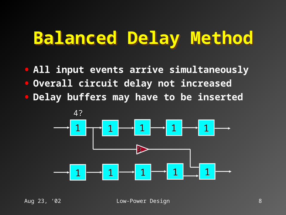
Balanced Delay MethodBalanced Delay Method
• All input events arrive simultaneously
• Overall circuit delay not increased
• Delay buffers may have to be inserted
11 111111 11
111111
33
11 11
4?4?

Aug 23, ‘02 9Low-Power Design
Hazard Filter MethodHazard Filter Method• Gate delay is made greater than maximum input path
delay difference
• No delay buffers needed (least transient energy)
• Overall circuit delay may increase
22 111111 11
22111111 11
1?1?3?3?

Aug 23, ‘02 10Low-Power Design
Linear ProgramLinear Program
• Variables: gate and buffer delays
• Objective: minimize number of buffers
• Subject to: overall circuit delay
• Subject to: minimum transient condition for multi-input gates
• AMPL, MINOS 5.5 (Fourer, Gay and Kernighan)

Limitation of this LPLimitation of this LP
• Constraints are written by path
enumeration.
• Since number of paths in a circuit is
exponential in circuit size, the formulation
is infeasible for large circuits.
• Example: c880 has 6.96M constraints.

New linear programming modelNew linear programming model
• Introduce two new variables per gate output:
• ti Earliest time of signal transition at gate i.
• Ti Latest time of signal transition at gate i.
t1, T1
tn, Tn
.
.
.
ti, Ti

Timing windowTiming window
Input signals transition within intervals [ ti , Ti ]
Output transition interval = [ t1 , Tn+d ]

New linear programNew linear program
• Gate variables d4..d12
• Buffer Variables d15..d29
• Corresponding window variables t4..t29 and T4..T29.

Gate constraints – multiple inputsGate constraints – multiple inputs
For Gate 7:
T7 > T5 + d7; t7 < t5 + d7; d7 > T7 - t7;
T7 > T6 + d7; t7 < t6 + d7;

Gate constraints – single inputGate constraints – single input
T16 + d19 = T19 ;
t16 + d19 = t19 ;
Buffer 19:

Overall delay constraintsOverall delay constraints
T11 < maxdelay
T12 < maxdelay

Validation of the modelValidation of the model
For Gate 6 (old model):
d1 + d3 – d2 < d6
d2 – d3 – d1 < d6

Validation of the modelValidation of the model
For Gate 6 (new model):
T6 > T2 + d6; t6 < t2 + d6; d6 > T6 - t6;
T6 > T3 + d6; t6 < t3 + d6; .. (Ineq. set A)

Validation of the modelValidation of the model
Buffer Constraints:
T2 = t2 = d2 ; T3 = t3 = d3 ; (Ineq. set B)
Substituting Ineq. set B in Ineq. set A
t6 – d2 < d6 ..( 1 )
t6 – d1 – d3< d6 ..( 2 )
d6 < T6 – d2 ..( 3 )
d6 < T6 – d1 – d3 ..( 4 )

Validation of the modelValidation of the modelAdding inequalities ( 1 ) and ( 4 )
d1 + d3 – d2 < T6 – t6
Adding inequalities ( 2 ) and ( 3 )
d2 - d3 – d1 < T6 – t6
• These are the same inequalities from the old model.
• Similar derivation can be done for maxdelay constraints too.
• Hence the new model constraints are equivalent to the old ones.

Why this model is superior?Why this model is superior?
• Path constraints from old model
4 × 4 × …4 = 4n
• Constraints from new model
15 × n = 15n
• Hence new constraint set is linear in size of circuit.

Comparison of constraint setsComparison of constraint sets
Number of gates in circuit
Nu
mb
er o
f co
nst
rain
ts
c880
3,611
6.96x10⁶

Results: Procedure outlineResults: Procedure outline
C++ Program
AMPL
Power Estimator
Combinational circuit netlist
Results
Constraint-set
Optimized delays

Results – 1 bit adderResults – 1 bit adder

Estimation of powerEstimation of power• Circuit is simulated by an event-driven
simulator for both optimized and un-optimized gate delays.
• All transitions at a gate are counted as Events[gate].
• Power consumed Events[gate] x # of fanouts.
• Reference: “Effects of delay model on peak power estimation of VLSI circuits,” Hsiao, et al. (ISLPED`97).

1-bit Adder: Transitions 1-bit Adder: Transitions
Nu
mb
er o
f tr
ansi
tion
s
Vector-pair in octal Vector-pair in octal
01 07 17 27 37 47 57 67 77 01 07 17 27 37 47 57 67 77
15
10
5
0
Avg =5.10 Avg =4.01
Unit-delays Optimized delays

Results: 1-bit adderResults: 1-bit adder
Colo
r co
des
for
num
ber
of
transi
tions

Results: 1-bit adderResults: 1-bit adder
Colo
r co
des
for
num
ber
of
transi
tions

Results: 1-bit adder
Simulated over all possible vector transitions
•Average power = optimized/unit delay = 244 / 308 = 0.792
•Peak power = optimized/unit delay = 6 / 10 = 0.60
Power Savings :
Peak = 40 %
Average = 21 %

Results: 4-bit ALUResults: 4-bit ALU
maxdelay Buffers inserted
7 5
10 2
12 1
15 0Simulation with 1,000 random vectors:
•Average power = optimized/unit delay = 2431 / 3060 = 0.794
•Peak power = optimized/unit delay = 28 / 42 = 0.66
Power Savings : Peak = 33 %, Average = 21 %

ConclusionConclusion• Obtained an LP constraint-set that is linear in the size of the
circuit. LP solution:
• Eliminates glitches at all gate outputs,
• Holds I/O delay within specification, and
• Combines path-balancing and hazard-filtering to minimize
the number of delay buffers.
• New LP produces results exactly identical to old LP requiring
exponential constraint-set.
• Results show peak power savings up to 40% and average
power savings up to 21%.