Audio Spectrum Analyzer Final Report - Harvey Mudd...
30
Audio Spectrum Analyzer Final Report Corey O’Connor Josh Smallman December 15, 2003
-
Upload
nguyenquynh -
Category
Documents
-
view
220 -
download
1
Transcript of Audio Spectrum Analyzer Final Report - Harvey Mudd...

Audio Spectrum AnalyzerFinal Report
Corey O’ConnorJosh Smallman
December 15, 2003

Abstract
Our final project was to build a simple audio spectrum analyzer. The device will take line-level stereo audio input and display the spectrum on a bank of LED arrays. There will beseven frequency bands for both the left and right channels for a total of 14 bands. The firstmajor element of our system is the input processing section. This section is responsible forsplitting the audio signal into the 14 bands with 7 parallel bandpass filters for each channel.This section then multiplexes the signals into a PIC through a set of logarithmic convertersfor sampling. The sampled values are then sent serially to the FPGA which drives a seriesof multiplexed LED arrays.
We successfully completed the PIC program, the input multiplexing, and the FPGA LEDdriver. We were unable to complete the bandpass filters for the input processing section.Instead we simplified the hardware to monitor amplitudes of 8 distinct stereo inputs. Wealso designed and built a custom PC board for our LED display.

Introduction
When working with audio it’s important to have good feedback. The frequency spectrumof an audio signal is useful for finding which component frequencies might be too loud ortoo soft to in order to get a properly equalized and balanced audio source.. Having a stand-alone system to display the spectrum from standard audio sources is a useful tool for anybodyworking with audio.
Our system is composed of an input processing section, a PIC for sampling, and an FPGAconfigured as an LED display controller. Our initial plan for the input processing sectionwould take a stereo input and first separate each channel into seven separate bands. Givena stereo signal this would of made a total of 14 bands. Each copy of the signal would havebeen processed by a set of bandpass filters and then logarithmic converters before beingsampled by the PIC. The logarithmic converters would have converted the AC signal intoa DC representation of the volume. Each channel would have had the same set of sevenbandpass filters which would have been configured with center frequencies approximatelyequal to: 60 Hz, 120 Hz, 400 Hz, 1 kHz, 2.5 kHz, 6.25 kHz, and 16 kHz.
The system we actually built was designed to handle 8 separate stereo inputs instead ofone input split into 7 frequency bands per channel. Instead of using logarithmic conversionto get the volume level we sampled the half-wave rectification to get the amplitude of thesignals.
The PIC microcontroller is used to sample from each input 30 times a second. This meansthe PIC would have sampled at 420 Hz in order to sample 14 inputs at the desired rate.Since we actually built the system to handle 8 stereo inputs this means the PIC must sampleat 480 Hz. The PIC is also responsible for controlling the multiplexing IC’s since there arenot enough physical connectors on the PIC’s A-to-D port to handle more than 8 inputs atonce. Once a given input has been sampled the value is sent over the serial line to the FPGA.The PIC samples to a 10 bit resolution, but only the top 8 bits are sent since this is moreconvenient and we only needed the top 4 bits for our bargraph-style display.
The FPGA is continuously multiplexing the LED arrays for the display where each LEDarray represents a value from the PIC. The LED arrays are driven in groups of two at atime: One array for the left channel, one for the right channel. After 8 FPGA clock cyclesthe next two LED arrays for the next two inputs are driven. This repeats indefinitely. Eachvalue received over the serial line is written into a register file containing the current valuesfor each input.
1

New Hardware
The PIC only has 8 analog inputs, and we needed 16. In order to sample from all 16 inputswe used two eight-channel analog multiplexers. These are essentially an SP8T solid stateswitch. The CS4051 set of chips implement this nicely for a cheap price. For our project weused the MC140551B (Which is equivalent to the CS4051). These worked well, except asside test revealed these are unsuitable for multiplexing the audio input directly. They had afrequency response that attenuated the higher frequencies significantly.
The bandpass filters were to be implemented using a set of active filters. We chose aresistor programmable universal filter IC. These are active filters that can operate as aseveral different types of filters. Exactly which filters an active filter IC implements dependslargely on the manufacturer. There are several varieties available, but we chose the MixedSignal Integration MSU2F. These are dual filter, switch-capacitor, resistor programmableIC’s. They can implement lowpass, highpass, bandpass and allpass among other things. Oneach IC, both filter’s center or cutoff frequency depends on the frequency of the clock inputtimes some multiplier.
The MSU2F promised to be an extremely flexible chip. With a clock programmablecenter frequency we could use a single IC to implement several different bandpass filters.Simply changing the input clock would change the center frequency. Sadly the datasheet wasinconsistent and very unclear. For instance, The symbol f0 is used to represent a constant,the input for a clock multiplier setting, and the center frequency. In fact the input voltagesfor the clock were specified as 0 to 2.5 volts for dual supply on the datasheet, but should havebeen specified as -2.5 to 2.5 volts. Even with tech support from Mixed Signal Interactionswe were unable to get the filters operating correctly. A better choice would have been to usethe LMF100 from National Semiconductor, or one of the many similar chips from MaximIC. The datasheets for both IC’s are very clear and helpful.
2

Schematics
Figure 1 shows the schematic for a multiplexing circuit containing 2 channels of 8 LEDarrays. Each single LED array consists of 10 LEDs, connected in a common-anode config-uration. Each LED is either on or off, depending on which pin is pulled high or low. Pins1-10 of the standard IDE ribbon cable connector control the value displayed on the left,while pins 31-40 control the right side. Each line is pulled through a 330 Ohm resistor toprevent too much current from flowing through the the LEDs. Pins 13-20 receive a one-coldsignal that ensures that only one PNP transistor is open, allowing only a single array fromeach side to be active at any moment in time. The base of each transistor is connected tothe FPGA through a 4.7K ohm resistor to limit the amount of current flowing into the basewhen we drive it low.
Figure 2 details the layout of the PCB we constructed that contains the circuit of Figure1. We used single-sided copper clad board and the Press-n-Peel resist transfer system inorder to construct the board. Since we used single-sided board, the red traces had to bemade manually with jumper wires.
Figure 3 shows the schematic of the circuit we breadboarded for the final demonstration.It shows the connection of 8 stereo line-level audio inputs to 2 8-channel analog multiplexers.The select controls of the multiplexers are set by 3 incoming data lines from PortB of thePIC. The outputs of each multiplexer run through a half-wave rectifier circuit in order toconvert the AC audio signal into a DC signal representing the amplitude of the signal,therefore giving some indication of the volume level of the audio input. The output of eachof the half-wave rectifiers are routed directly into A/D inputs 1 and 2 of the PIC, wherethey are sampled according to a reference voltage input obtained through a 1k potentiometerconnected to A/D input 3. The signal is also routed through a lowpass filter with a cutofffrequency at around 34 kHz. This eliminates any clock or multiplexer noise from the signal.The rest of the figure details the FPGA’s pin output connections to the 40-pin ribbon cablethat connects the breadboard to the LED Array PCB (Fig. 2)
3
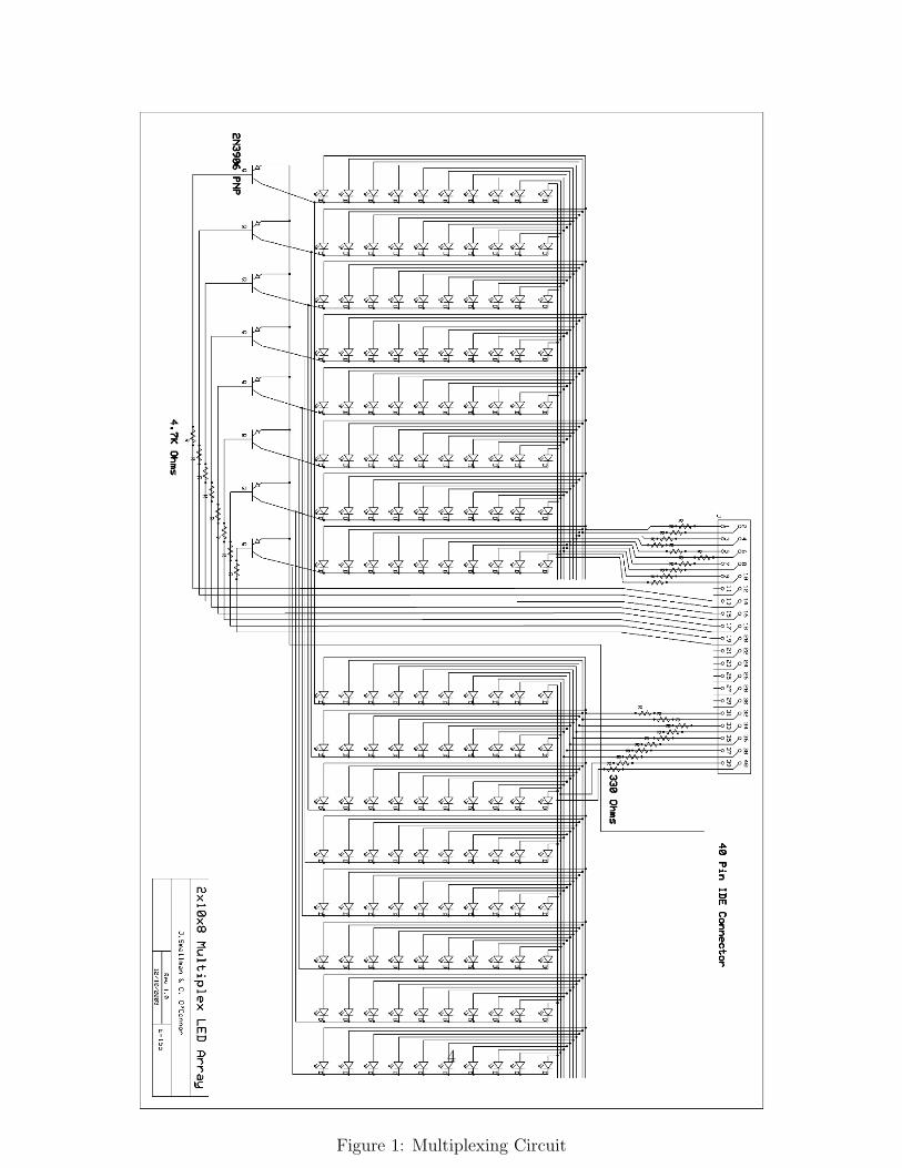
Figure 1: Multiplexing Circuit
4

Figure 2: PCB Circuit
5
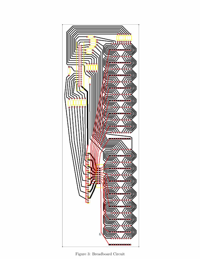
Figure 3: Breadboard Circuit
6

Microcontroller Design
The PIC is responsible for sampling the input signal and controlling the input multiplexing.Each frequency band is sampled 30 times a second. For 16 bands that requires the PIC tosample from the A/D input port 480 times a second. Running off a 1 MHz clock means thetime to sample each band can at most take about 520 instruction cycles.
On startup InitializeSampleTimer is called to set up the timer and CCP. The CCP isconfigured to interrupt whenever Timer 1 reaches a value of 520. Then the A/D module isinitialized. Then InitializeInputControl is called to set up the input multiplexers to start onthe first band of each channel. Once all this has been initialized the interrupts are enabled,the timer is started, then the A/D conversion is started.
The CCP interrupt writes the sampled data to the serial port and changes what pin theA/D samples from. Although our code checks to insure the A/D has completed successfully,the conversion should always be completed by the time the CCP interrupt fires. This waywe don’t need to use the A/D interrupt also. Every time the PIC is set to sample from theleft channel’s input the program calls NextBand to increment the output that controls theanalog multiplexers. Then the timer is reset and the A/D conversion is started again.
7

FPGA Design
The FPGA has two primary responsibilities in this design. It monitors an incoming serialdata line and a serial data clock input, grabbing 8 bit words and storing the top 4 bits intoone of 16 allocated registers. Its other function is to write the incoming data values to amultiplexed display consisting of 16 LED arrays.
The driver module consists of several sub-modules which perform its functionality. Themain module takes in a serial clock and serial data, and has 28 output pins. 10 pins controlthe the 10 LEDs in a single LED array via display output left/right, while an additional 8pins assigned to display select control transistors that activate a single pair of LED arrays.
In order to slow down the 1MHz clock to a reasonable refresh rate for the display, theclkDivideBy8 module takes the clk input and outputs a reduced clock signal that is used todrive the multiplexed arrays. It also creates a 3 on 1 off duty cycled display enable signal,which is used to reduce bleed through that is associated with multiplexed displays. TheDisplaySelectGen module takes the divided clock and generates a one-cold 8 bit signal thatindicates which of the 8 arrays is currently active.
Our GetSerialData module shifts in bits that come in over the serial data line as theserial clk wiggles asynchronously. The top 4 bits of the incoming word are assigned toserial data word, and every time 8 bits has been received, the serial data rx flag is raised toindicate that serial data word contains a valid value.
The synchro module takes the output of GetSerialData and synchronizes its signals beforepassing them on to the BandRegisters module. BandRegisters contains 2 arrays of 8 4-bitregisters, called L and R, which are used to store the 16 most recent data values receivedover the serial line. As each word comes into the module (after being synchronized) andthe serial data rxS flag is raised, BandRegisters updates the appropriate register and waitsfor the next word. Additionally, BandRegisters uses the one-cold display select signal todetermine which pair of LED arrays are currently active, and assigns current band out Rand current band out L the appropriate values extracted from the register array.
The two current band out L/R signals generated by BandRegisters are converted by twoincarnations of the BandLEDOutput module. The BandLEDOutput module takes the 4 bitinput and generates a 10-bit bargraph value, but with the applied 3 on 1 off duty cycle ofdisplay enable. That means that when display enable is low, BandLEDOutput will outputall 1’s, which turns off all 10 LED’s in an array. When display enable is high, it will outputthe converted value as determined by FourBitToBar, a simple module that performs theactual 4 to 10 bit conversion. The outputs of the two BandLedOutput modules directlydrive the 20 output pins of the FPGA.
8

display_select/8
GetSerialDataserial_data
serial_clk
BandLEDOutput
clkDivideBy8
FourBitToBar
BandLEDOutput
R1-R8L1-L8
DisplaySelectGen
display_output_left/10 display_output_right/10
Synchroserial_data_rx
serial_data_word/4
ChannelRegisters
serial_data_wordSserial_data_rxS
divided_clk
current_band_L/10 current_band_R/10display_enable
FourBitToBar
Figure 4: FPGA Block Diagram
9

Results
Our project resulted in the creation several components, which when put together form afunctional 16 channel audio analyzer and display.
Originally, we had planned on the input section composing of bandpass filters that woulddivide 1 stereo source into 14 signals, send each of the 14 signals through a logarithmicconverter to generate a voltage representing sound pressure, and finally multiplex the 14signals into 2 inputs on the PIC’s A/D. The first change we decided on was to increase thewidth of our analyzer to 8 channels per side instead of 7, since our analog multiplexer had 8inputs. Additionally, because we were unable to prototype a working bandpass filter circuit,we decided to input 8 distinct stereo signals into the system instead of generating the 16signals from a single pair. The final change from our original plan was in the use of a half-wave rectifier to convert the AC audio signal into a DC representation of volume. We foundthat multiplexing the logarithmic converters caused samples to bleed through to each other,because the setup time for the circuit was longer than our sample rate. By switching to ahalf wave rectifier, our value would vary linearly with the amplitude of the signal, instead ofthe logarithmic representation of sound pressure.
Our design for the PIC Microcontroller and FPGA remained in line with our originalplans, except for the expansion from 7 to 8 channels, since once the input is generated, howit is sampled, communicated, and displayed remains the same regardless of the nature ofthe data. The PIC controls the analog multiplexers, sampling each of the 8 stereo inputsthrough 2 of its A/D inputs, and sends the top 8 bits of the sample across the serial dataline. The FPGA receives the 8 bit words coming across the serial line, and stores the top 4bits in a register array. The FPGA also generates outputs to drive our custom made PCB,consisting of 16 multiplexed LED arrays and support resistors/transistors.
The most difficult challenges for this project were introduced by the analog circuits wewanted to use for signal preparation. We invested a significant portion of our effort (andbudget) into the bandpass filters, but eventually had to abandon their use as our deadlineapproached. Although we had identified the analog section as a risk, we took too long todecide that an alternative approach to the problem was necessary. In the future, we shouldensure that all serious risks are navigated and handled as soon as possible, and be willing toseek alternatives sooner.
Using the LMF100 active filter IC would have been a better choice than the MSU2F.The LMF100 is a well established chip, and many examples exist how to use the IC. Thedatasheet is also significantly better with long discussions on exactly how the IC should beconfigured and connected for best performance. However, a distributor, manufacturer ordatasheet for this IC was not located until after the MSU2F’s had already been purchasedand shipped.
10

References
1. Horowitz and Hill. the Art of Electronics Cambridge, United Kingdom: CambridgeUniversity Press, 1989
2. Mixed Signal Interaction MSU2F Active Filter IC, http://www.mix-sig.com/MSUF.pdf
3. National Semiconductor LMF100, http://www.swarthmore.edu/NatSci/echeeve1/Ref/DataSheet/LMF100.pdf
4. Motorola MC14051B, http://www.fe.up.pt/~victorm/DataSheet/CMOS/mc14051brev3.pdf
Parts List
2x [Analog Multiplexer] Motorola MC14051B. from MarVac, http://www.marvac.com.$3.20
8x [Analog Bandpass Filters] MSU2F. From Mixed Signal Interactions, (408)-434-6305$34.34
11
Appendices
PIC Microcontroller program: multi sampler.asm
; Author: Corey O’Connor ([email protected]) & Josh Smallman ([email protected])
; File: multi_sampler.asm
; 11/18/2003
; This program alternates between sampling from two A/D ports.
; The top 8-bits of the samples are then communicated over the serial line.
; Uses bits 0-2 of PortB to control two 8-input analog multiplexers, where the
; output of each is connected to A/D inputs 1 and 2. Vref is provided by I/O 3 of the A/D.
; Essentially, this program takes 8-bit samples from 16 different analog inputs and outputs
; them in order and repeatedly over the serial line.
LIST p=18F452
include "p18f452.inc"
SAMPLE_RATE EQU D’520’
LEFT_CHANNEL EQU 0
RIGHT_CHANNEL EQU 1
nextValueToSend RES 1
currentChannel RES 1
currentBand RES 1
org 0
bra start
; High priority interrupt vector
org 8
btfsc PIR1, CCP1IF
bra CCPInterrupt
retfie
CCPInterrupt
; Clear interrupt flag
bcf PIR1, CCP1IF
; Skip this if the A/D is incomplete
btfsc ADCON0, GO
12

bra CCPTimerReset
; Send the current value over the serial port
movff ADRESH, SSPBUF
; noop until the word is sent.
nop
nop
nop
nop
nop
nop
nop
nop
nop
nop
; Set the A/D to sample from the other channel
comf currentChannel
btfsc currentChannel, 0
bra SampleFromRight
; Sample from left channel
bcf ADCON0, CHS0
call NextBand
bra StartSampling
SampleFromRight
; Sample from right channel
bsf ADCON0, CHS0
StartSampling
; Start the sampling
bsf ADCON0, GO
CCPTimerReset
; Restart the timer
movlw high SAMPLE_RATE
movwf TMR1H
13

movlw low SAMPLE_RATE
movwf TMR1L
retfie
; start of the main program
start
; Initialize serial line
; Set port C for output
clrf TRISC
; Configure the serial port register
; Set bit 5: Enable
; Clear bit 4: clock idle state is low
; Clear bits 0-3: osc/4 clock
; Clear bits 6,7: Clear overflow and collision flags.
movlw B’00100000’
movwf SSPCON1
; Configure the serial port status
; Set bit 7: Master mode
; Set bit 6: Data transmitted on rising edge of SCK
movlw B’11000000’
movwf SSPSTAT
; Set current channel and band
movlw LEFT_CHANNEL
movwf currentChannel
movlw 0
movwf currentBand
; Initialize multiplexed input control
call InitializeInputControl, 1
; Initialize CCP and a timer to interrupt at the correct sampling rate
call InitializeSamplingTimer, 1
; Initialize A/D port
; Set pins 0 and 1 on porta for input
bsf TRISA, 0
bsf TRISA, 1
14

; Configure ADCON0
; clear bits 7-6: Set Tad to Fosc/4
; clear bits 5-3: Sampling AN0 (left channel)
; set bit 0: Turn on A/D module.
movlw B’00000001’
movwf ADCON0
; Configure ADCON1
; clear bit 7: Left justify result
; set bit 6: tad = Fosc/4
; clear bits 3-1: AN0 & AN1 as analog inputs, bit 0 high makes AN3 into VREF+
movlw B’01000001’
movwf ADCON1
; Start sampling
bsf ADCON0, GO
; Start the timer
bsf T1CON, 0
; Enable interrupts
bsf INTCON, GIE
bsf INTCON, PEIE
; Loop
end_loop
bra end_loop
InitializeInputControl
; Set current band of left and right channels to 0
; Reset the filters if nescessary
; Set port B for output
bcf TRISB, 0
bcf TRISB, 1
bcf TRISB, 2
movlw 0
movwf PORTB
return 1
15

InitializeSamplingTimer
; Initialize Timer 1
; Set bit 7
; Clear bits 4,5: 1:1 prescale
; Clear bit 1: Internal clock
; Don’t start the timer yet
movlw B’10000000’
movwf T1CON
; Initialize CCP
; Set bits 3-0 to 1010: Compare mode. Interrupt on match
movlw B’00001010’
movwf CCP1CON
; Set timer 1 as clock source for CCP1
bcf T3CON, 6
bcf T3CON, 3
; Set the compare value so the interrupt fires every 1200 instructions.
movlw high SAMPLE_RATE
movwf CCPR1H
movlw low SAMPLE_RATE
movwf CCPR1L
; Initialize interrupts
; Clear interrupt flag
bcf PIR1, CCP1IF
; Enable CCP compare interrupts
bsf PIE1, CCP1IE
return 1
NextBand
; Add one to currentChannel
incf currentBand
movff currentBand, PORTB
return 1
end
16

Main Verilog module: driver.v
// driver.v, a Display Driver for a custom Multiplexed LED Array PCB.
// Written by Corey O’Connor ([email protected]) & Josh Smallman ([email protected])
// 11/18/2003
// This module is used to receive a repeating series of 16 8-bit words via a serial interface.
// It displays the top 4 bits of each word in bargraph mode on one of 16 LED Arrays.
module driver(clk, reset,
serial_data, serial_clk,
display_select,
display_output_left, display_output_right);
input clk;
input reset;
input serial_clk;
input serial_data;
output [7:0] display_select; // one-cold controls which of the 8 pairs of LED Arrays are active via PNP Transistor
output [9:0] display_output_left; // 10-bit value that is written bitwise to the 10 LEDs in the currently active array.
output [9:0] display_output_right; // Since one array from each side is displayed at once, each side has its own 10 outputs.
wire divided_clk; // slow down the clock for a reasonable refresh rate
wire display_enable; // duty cycle (3 on 1 off) the display to reduce blur between multiplexed outputs.
wire [3:0] current_band_L, current_band_R;
wire [3:0] serial_data_word; // the word that just came in over the serial line
wire serial_data_rx; // indicates a complete word has been received
wire [3:0] serial_data_wordS; // holds synchronized complete word
wire serial_data_rxS; // holds synchronized serial_data_rx flag
/* filterDriver filterDriver(clk, reset, filter_clock);*/
// create the divided clock and display enable signals
clkDivideBy8 clkDivideBy8(clk, reset, divided_clk, display_enable);
// create the display_select signal
DisplaySelectGen DisplaySelectGen(clk, reset, divided_clk, display_select);
// shift in serial data from the serial line and put words into serial_data_word
// Also raises serial_data_rx flag
GetSerialData GetSerialData(serial_clk, reset, serial_data,
serial_data_word, serial_data_rx, clk);
17

// synchronize the serial data, since the serial_clk input is asynchronous
Synchro Synchro(clk, reset, serial_clk, serial_data_word, serial_data_rx,
serial_data_wordS, serial_data_rxS);
// stores incoming words in an array of registers, and outputs what 4 bit values should be
// displayed on the 2 currently active LED arrays.
BandRegisters ChannelRegisters(clk, reset,
divided_clk, display_select,
serial_data_rxS, serial_data_wordS,
current_band_L, current_band_R);
// convert the 4-bit output of BandRegisters to the 10-bit value we need for display on an LED array
BandLEDOutput leftChannelOutput(current_band_L,
display_enable,
display_output_left);
BandLEDOutput rightChannelOutput(current_band_R,
display_enable,
display_output_right);
endmodule
18

clkDivideBy8.v
// clkDivideBy8.v
// Written by Corey O’Connor ([email protected]) & Josh Smallman ([email protected])
// 11/18/2003
// Standard Clock divider, also creates an enable output with a duty cycle
// of 3 on 1 off.
module clkDivideBy8(clk,reset,out, enable);
input clk;
input reset;
output out;
output enable;
reg [1:0] state;
always @(posedge clk or posedge reset)
if (reset) state <= 2’b000;
//else if (state == 3’b111) state <= 3’b000;
else state <= state + 1;
assign out = ~state[1];
assign enable = state[0] | state[1];
endmodule
19

DisplaySelectGen.v
// DisplaySelectGen.v
// Written by Corey O’Connor ([email protected]) & Josh Smallman ([email protected])
// 11/18/2003
// Creates a one-cold 8 bit output that left shifts on positive edges of the shift input.
module DisplaySelectGen(clk,reset, shift, display_select);
input clk;
input reset;
input shift;
output [7:0] display_select;
reg [7:0] display_select;
always @(posedge reset or posedge shift)
begin
if(reset)
display_select <= 8’b11111110;
else if(shift)
display_select <= {display_select[6:0], display_select[7]};
end
endmodule
20

GetSerialData.v
// GetSerialData.v
// Written by Corey O’Connor ([email protected]) & Josh Smallman ([email protected])
// 11/18/2003
// This module shifts in serial data and stores each 8-bits as a word.
// Outputs top 4 bits of each incoming word.
// Also raises a flag when an entire 8-bit word has been captured.
module GetSerialData(serial_clk,reset,serial_data,serial_data_word,serial_data_rx, clk);
input clk;
input serial_clk;
input reset;
input serial_data;
output [3:0] serial_data_word;
output serial_data_rx;
reg [2:0] word_size; // counter for how big the word should be
reg [7:0] shiftreg; // stores each bit as it comes in
reg started; // ignore the high serial_clk input it goes down first
// and back up with a rising edge
always@(posedge reset or posedge serial_clk)
begin
if (reset)
begin
word_size <= 0;
shiftreg <= 0;
started <= 0;
end
else
begin
shiftreg <= {shiftreg[6:0],serial_data};
word_size <= word_size + 1;
started <=1;
end
end
// output the top 4 bits of the incoming word, and create the rx flag.
assign serial_data_word = shiftreg[7:4],
serial_data_rx = (word_size == 3’b000) & (started == 1);
endmodule
21

Synchro.v
// Synchro.v
// Written by Corey O’Connor ([email protected]) & Josh Smallman ([email protected])
// 11/18/2003
// Synchronizes the asynchronous serial_data_word and serial_data_rx inputs
// Outputs the synchronized signals.
module Synchro(clk,reset,serial_clk,serial_data_word,serial_data_rx,serial_data_wordS,
serial_data_rxS);
input clk;
input reset;
input serial_clk;
input [3:0] serial_data_word;
input serial_data_rx;
output [3:0] serial_data_wordS;
output serial_data_rxS;
reg [3:0] serial_data_wordS;
reg serial_data_rxS;
always@(posedge reset or posedge clk)
begin
if (reset)
begin
serial_data_wordS <= 4’b0;
serial_data_rxS <= 1’b0;
end
else
begin
if(serial_clk)
begin
serial_data_rxS <= serial_data_rxS ? 0 : serial_data_rx;
serial_data_wordS <= serial_data_word;
end
end
end
endmodule
22

BandRegisters.v
// BandRegisters.v
// Written by Corey O’Connor ([email protected]) & Josh Smallman ([email protected])
// 11/18/2003
// This module receives repeating loops of 16 4-bit words and stores them in one of
// sixteen 4-bit registers. It also outputs the two 4-bit words according to the
// one-cold encoding of the display_select input.
module BandRegisters(clk,reset,divided_clk,display_select,serial_data_rxS,
serial_data_wordS,current_band_out_L,current_band_out_R);
input clk;
input reset;
input divided_clk;
input [7:0] display_select; // one-cold encoding of which pair of LED arrays are active
input serial_data_rxS; // synchronized flag indicating complete word received
input [3:0] serial_data_wordS; // synchronized word received.
output [3:0] current_band_out_L; // the value to be displayed on the currently active left array
output [3:0] current_band_out_R; // the value to be displayed on the currently active right array
reg [3:0] R[0:7]; // array of 8 registers, each holding 4 bit value to be displayed on an LED array
reg [3:0] L[0:7]; // array for left side
reg [1:0] state; // state variable used to ensure proper serial word receipt and processing.
// this points to which register is next to be
// updated from the incoming word on the serial line
reg [3:0] current_serial_to_register;
always @(posedge reset or posedge clk)
begin
if(reset)
begin
// Set starting values, display ramp on board
state <= 2’b00;
current_serial_to_register <= 4’b0;
L[0] <= 4’b0001;
L[1] <= 4’b0010;
L[2] <= 4’b0011;
L[3] <= 4’b0100;
L[4] <= 4’b0101;
L[5] <= 4’b0110;
L[6] <= 4’b0111;
L[7] <= 4’b1000;
23

R[0] <= 4’b1001;
R[1] <= 4’b1010;
R[2] <= 4’b1011;
R[3] <= 4’b1100;
R[4] <= 4’b1101;
R[5] <= 4’b1110;
R[6] <= 4’b1111;
R[7] <= 4’b0000;
end
else
// this code ensures that each word that comes in over the serial line
// is only received once.
case(state)
2’b00: // starting state
begin
if(serial_data_rxS) // if we’ve received a word
begin
if(current_serial_to_register[0] == 0) // put the word into the right register
L[current_serial_to_register[3:1]] <= serial_data_wordS;
else
R[current_serial_to_register[3:1]] <= serial_data_wordS;
state <= 2’b01; // increment state
end
end
2’b01: // second state, just put word into register.
begin
// increment the pointer to the next register to be updated
current_serial_to_register <= current_serial_to_register + 1;
state <= 2’b10; // increment state
end
2’b10: // third state, stay in third state until serial_data_rxS flag goes back down.
if(serial_data_rxS)
state <= 2’b10;
else
state <= 2’b00;
endcase
end
// assign the value pointed to by display_select to the current_band_out outputs.
assign current_band_out_R = (display_select[0] == 0) ? R[0] : {4{1’bz}},
current_band_out_R = (display_select[1] == 0) ? R[1] : {4{1’bz}},
current_band_out_R = (display_select[2] == 0) ? R[2] : {4{1’bz}},
current_band_out_R = (display_select[3] == 0) ? R[3] : {4{1’bz}},
24
current_band_out_R = (display_select[4] == 0) ? R[4] : {4{1’bz}},
current_band_out_R = (display_select[5] == 0) ? R[5] : {4{1’bz}},
current_band_out_R = (display_select[6] == 0) ? R[6] : {4{1’bz}},
current_band_out_R = (display_select[7] == 0) ? R[7] : {4{1’bz}};
assign current_band_out_L = (display_select[0] == 0) ? L[0] : {4{1’bz}},
current_band_out_L = (display_select[1] == 0) ? L[1] : {4{1’bz}},
current_band_out_L = (display_select[2] == 0) ? L[2] : {4{1’bz}},
current_band_out_L = (display_select[3] == 0) ? L[3] : {4{1’bz}},
current_band_out_L = (display_select[4] == 0) ? L[4] : {4{1’bz}},
current_band_out_L = (display_select[5] == 0) ? L[5] : {4{1’bz}},
current_band_out_L = (display_select[6] == 0) ? L[6] : {4{1’bz}},
current_band_out_L = (display_select[7] == 0) ? L[7] : {4{1’bz}};
endmodule
25

BandLEDOutput.v
// BandLEDOutput.v,
// Written by Corey O’Connor ([email protected]) & Josh Smallman ([email protected])
// 11/18/2003
// This module takes a 2 4bit inputs and converts them to a 10 bit bargraph value
// All the work is done by the FourBitToBar module
module BandLEDOutput(current_band,display_enable,display_out);
input [3:0] current_band;
input display_enable;
output [9:0] display_out;
wire [9:0] converted_value;
FourBitToBar FourBitToBar(current_band, converted_value);
assign display_out = display_enable ? converted_value : {10{1’b1}};
endmodule
26

FourBitToBar.v
// FourBitToBar.v, a Display Driver for a custom Multiplexed LED Array PCB.
// Written by Corey O’Connor ([email protected]) & Josh Smallman ([email protected])
// 11/18/2003
// Takes a 4 bit input and outputs a bargraph encoded 10-bit value.
module FourBitToBar(data, bar_out);
input [3:0] data;
output [9:0] bar_out;
reg [9:0] bar_out;
parameter ZERO = {10{1’b1}};
parameter ONE = 10’b1111111110;
parameter TWO = 10’b1111111100;
parameter THREE = 10’b1111111000;
parameter FOUR = 10’b1111110000;
parameter FIVE = 10’b1111100000;
parameter SIX = 10’b1111000000;
parameter SEVEN = 10’b1110000000;
parameter EIGHT = 10’b1100000000;
parameter NINE = 10’b1000000000;
parameter TEN = 10’b0000000000;
always @(data)
case(data)
4’b0000: bar_out <= ZERO;
4’b0001: bar_out <= ONE;
4’b0010: bar_out <= ONE;
4’b0011: bar_out <= TWO;
4’b0100: bar_out <= THREE;
4’b0101: bar_out <= THREE;
4’b0110: bar_out <= FOUR;
4’b0111: bar_out <= FIVE;
4’b1000: bar_out <= FIVE;
4’b1001: bar_out <= SIX;
4’b1010: bar_out <= SEVEN;
4’b1011: bar_out <= SEVEN;
4’b1100: bar_out <= EIGHT;
4’b1101: bar_out <= NINE;
4’b1110: bar_out <= NINE;
4’b1111: bar_out <= TEN;
27

default: bar_out <= TEN;
endcase
endmodule
28