at90usb162
306
Features • High Performance, Low Power AVR ® 8-Bit Microcontroller • Advanced RISC Architecture – 125 Powerful Instructions – Most Single Clock Cycle Execution – 32 x 8 General Purpose Working Registers – Fully Static Operation – Up to 16 MIPS Throughput at 16 MHz • Non-volatile Program and Data Memories – 8K / 16K Bytes of In-System Self-Programmable Flash • Endurance: 10,000 Write/Erase Cycles – Optional Boot Code Section with Independent Lock Bits • USB boot-loader programmed by default in the factory • In-System Programming by on-chip Boot Program hardware-activated after reset • True Read-While-Write Operation – 512 Bytes EEPROM • Endurance: 100,000 Write/Erase Cycles – 512 Bytes Internal SRAM – Programming Lock for Software Security • USB 2.0 Full-speed Device Module with Interrupt on Transfer Completion – Complies fully with Universal Serial Bus Specification REV 2.0 – 48 MHz PLL for Full-speed Bus Operation : data transfer rates at 12 Mbit/s – Fully independant 176 bytes USB DPRAM for endpoint memory allocation – Endpoint 0 for Control Transfers: from 8 up to 64-bytes – 4 Programmable Endpoints: • IN or Out Directions • Bulk, Interrupt and IsochronousTransfers • Programmable maximum packet size from 8 to 64 bytes • Programmable single or double buffer – Suspend/Resume Interrupts – Microcontroller reset on USB Bus Reset without detach – USB Bus Disconnection on Microcontroller Request – USB pad multiplexed with PS/2 peripheral for single cable capability • Peripheral Features – PS/2 compliant pad – One 8-bit Timer/Counters with Separate Prescaler and Compare Mode (two 8-bit PWM channels) – One 16-bit Timer/Counter with Separate Prescaler, Compare and Capture Mode (three 8-bit PWM channels) – USART with SPI master only mode and hardware flow control (RTS/CTS) – Master/Slave SPI Serial Interface – Programmable Watchdog Timer with Separate On-chip Oscillator – On-chip Analog Comparator – Interrupt and Wake-up on Pin Change • On Chip Debug Interface (debugWIRE) • Special Microcontroller Features – Power-On Reset and Programmable Brown-out Detection – Internal Calibrated Oscillator – External and Internal Interrupt Sources 8-bit Microcontroller with 8/16K Bytes of ISP Flash and USB Controller AT90USB82 AT90USB162 7707D–AVR–07/08
Transcript of at90usb162

8-bit Microcontroller with 8/16K Bytes of ISP Flash and USB Controller
AT90USB82 AT90USB162
7707D–AVR–07/08
Features• High Performance, Low Power AVR® 8-Bit Microcontroller• Advanced RISC Architecture
– 125 Powerful Instructions – Most Single Clock Cycle Execution– 32 x 8 General Purpose Working Registers– Fully Static Operation– Up to 16 MIPS Throughput at 16 MHz
• Non-volatile Program and Data Memories– 8K / 16K Bytes of In-System Self-Programmable Flash
• Endurance: 10,000 Write/Erase Cycles– Optional Boot Code Section with Independent Lock Bits
• USB boot-loader programmed by default in the factory• In-System Programming by on-chip Boot Program hardware-activated after
reset• True Read-While-Write Operation
– 512 Bytes EEPROM• Endurance: 100,000 Write/Erase Cycles
– 512 Bytes Internal SRAM– Programming Lock for Software Security
• USB 2.0 Full-speed Device Module with Interrupt on Transfer Completion– Complies fully with Universal Serial Bus Specification REV 2.0– 48 MHz PLL for Full-speed Bus Operation : data transfer rates at 12 Mbit/s– Fully independant 176 bytes USB DPRAM for endpoint memory allocation– Endpoint 0 for Control Transfers: from 8 up to 64-bytes– 4 Programmable Endpoints:
• IN or Out Directions• Bulk, Interrupt and IsochronousTransfers• Programmable maximum packet size from 8 to 64 bytes• Programmable single or double buffer
– Suspend/Resume Interrupts– Microcontroller reset on USB Bus Reset without detach– USB Bus Disconnection on Microcontroller Request– USB pad multiplexed with PS/2 peripheral for single cable capability
• Peripheral Features– PS/2 compliant pad– One 8-bit Timer/Counters with Separate Prescaler and Compare Mode (two 8-bit
PWM channels)– One 16-bit Timer/Counter with Separate Prescaler, Compare and Capture Mode
(three 8-bit PWM channels)– USART with SPI master only mode and hardware flow control (RTS/CTS)– Master/Slave SPI Serial Interface– Programmable Watchdog Timer with Separate On-chip Oscillator– On-chip Analog Comparator– Interrupt and Wake-up on Pin Change
• On Chip Debug Interface (debugWIRE)• Special Microcontroller Features
– Power-On Reset and Programmable Brown-out Detection– Internal Calibrated Oscillator– External and Internal Interrupt Sources

– Five Sleep Modes: Idle, Power-save, Power-down, Standby, and Extended Standby• I/O and Packages
– 22 Programable I/O Lines– QFN32 (5x5mm) / TQFP32 packages
• Operating Voltages– 2.7 - 5.5V
• Operating temperature– Industrial (-40°C to +85°C)
• Maximum Frequency– 8 MHz at 2.7V - Industrial range– 16 MHz at 4.5V - Industrial range
27707D–AVR–07/08
AT90USB82/162

AT90USB82/162
1. Pin Configurations
Figure 1-1. Pinout AT90USB82/162
Note: The large center pad underneath the QFN packages is made of metal and must be connected to GND. It should be soldered or glued to the board to ensure good mechanical stability. If the center pad is left unconnected, the package might loosen from the board.
1.1 DisclaimerTypical values contained in this datasheet are based on simulations and characterization of other AVR microcontrollers manufactured on the same process technology. Min and Max values will be available after the device is characterized.
UV
CC
QFN32(PCINT11) PC2
(OC.0B / INT0) PD0
VCC
XTAL1
(IN
T5)
PD
4
(TX
D1
/ IN
T3)
PD
3
(XC
K /
PC
INT
12)
PD
5
PB3 (PDO / MISO / PCINT3)
GND(PC0) XTAL2
UG
ND
PB4 (T1 / PCINT4)
28 27 261234567
24232221201918
1211109 13 14 15
(AIN0 / INT1) PD1
816
17
PB6 (PCINT6)
D-
/ SD
ATA
D+
/ S
CK
2529303132
PB7 (PCINT7 / OC.0A / OC.1C)
PB5 (PCINT5)
PC7 (INT4 / ICP1 / CLKO)
PC6 (OC.1A / PCINT8)
Reset (PC1 / dW)
PC
5 (
PC
INT
9/ O
C.1
B)
PC
4 (P
CIN
T10
)U
CA
P
(RXD1 / AIN1 / INT2) PD2
(RT
S /
INT
6) P
D6
(CT
S /
HW
B /
T0
/ IN
T7)
PD
7
(SS
/ P
CIN
T0)
PB
0
(SC
LK /
PC
INT
1) P
B1
(PD
I / M
OS
I / P
CIN
T2)
PB
2
AV
CC
UV
CC
VQFP32(PCINT11) PC2
(OC.0B / INT0) PD0
VCC
XTAL1(I
NT
5) P
D4
(TX
D1
/ IN
T3)
PD
3
(XC
K /
PC
INT
12)
PD
5
PB3 (PDO / MISO / PCINT3)
GND(PC0) XTAL2
UG
ND
PB4 (T1 / PCINT4)
28 27 261234567
24232221201918
1211109 13 14 15
(AIN0 / INT1) PD1
816
17
PB6 (PCINT6)
D-
/ SD
ATA
D+
/ S
CK
2529303132
PB7 (PCINT7 / OC.0A / OC.1C)
PB5 (PCINT5)
PC7 (INT4 / ICP1 / CLKO)
PC6 (OC.1A / PCINT8)
Reset (PC1 / dW)
PC
5 (
PC
INT
9/ O
C.1
B)
PC
4 (P
CIN
T10
)U
CA
P
(RXD1 / AIN1 / INT2) PD2
(RT
S /
INT
6) P
D6
(CT
S /
HW
B /
T0
/ IN
T7)
PD
7
(SS
/ P
CIN
T0)
PB
0
(SC
LK /
PC
INT
1) P
B1
(PD
I / M
OS
I / P
CIN
T2)
PB
2
AV
CC
37707D–AVR–07/08

2. OverviewThe AT90USB82/162 is a low-power CMOS 8-bit microcontroller based on the AVR enhanced RISC architecture. By exe-cuting powerful instructions in a single clock cycle, the AT90USB82/162 achieves throughputs approaching 1 MIPS per MHz allowing the system designer to optimize power consumption versus processing speed.
2.1 Block Diagram
Figure 2-1. Block Diagram
The AVR core combines a rich instruction set with 32 general purpose working registers. All the 32 registers are directly connected to the Arithmetic Logic Unit (ALU), allowing two independent registers to be accessed in one single instruction executed in one clock cycle. The resulting
PROGRAMCOUNTER
STACKPOINTER
PROGRAMFLASH
MCU CONTROLREGISTER
SRAM
GENERALPURPOSE
REGISTERS
INSTRUCTIONREGISTER
TIMER/COUNTERS
INSTRUCTIONDECODER
DATA DIR.REG. PORTC
DATA REGISTERPORTC
INTERRUPTUNIT
EEPROM
USART1
STATUSREGISTER
Z
Y
X
ALU
PORTC DRIVERSPORTD DRIVERS PORTB DRIVERS
PC7 - PC0 PD7 - PD0
RE
SE
T
VCC
GND
XTA
L1
XTA
L2
CONTROLLINES
AN
AL
OG
CO
MP
AR
AT
OR
PB7 - PB0
D+/SCK
D-/SDATA
INTERNALOSCILLATOR
WATCHDOGTIMER
8-BIT DA TA BUS
USB
PS/2
TIMING ANDCONTROL
OSCILLATOR
CALIB. OSC
DATA DIR.REG. PORTB
DATA REGISTERPORTB
ON-CHIP DEBUG
Debug-Wire
PROGRAMMINGLOGIC
DATA DIR.REG. PORTD
DATA REGISTERPORTD
POR - BODRESET
PLL
+-
SPI
ON-CHIP3.3V
REGULATOR
UVcc
UCap
1uF
47707D–AVR–07/08
AT90USB82/162

AT90USB82/162
architecture is more code efficient while achieving throughputs up to ten times faster than con-ventional CISC microcontrollers.
The AT90USB82/162 provides the following features: 8K / 16K bytes of In-System Programma-ble Flash with Read-While-Write capabilities, 512 bytes EEPROM, 512 bytes SRAM, 22 general purpose I/O lines, 32 general purpose working registers, two flexible Timer/Counters with com-pare modes and PWM, one USART, a programmable Watchdog Timer with Internal Oscillator, an SPI serial port, debugWIRE interface, also used for accessing the On-chip Debug system and programming and five software selectable power saving modes. The Idle mode stops the CPU while allowing the SRAM, Timer/Counters, SPI port, and interrupt system to continue func-tioning. The Power-down mode saves the register contents but freezes the Oscillator, disabling all other chip functions until the next interrupt or Hardware Reset. In Standby mode, the Crys-tal/Resonator Oscillator is running while the rest of the device is sleeping. This allows very fast start-up combined with low power consumption. In Extended Standby mode, the main Oscillator continues to run.
The device is manufactured using Atmel’s high-density nonvolatile memory technology. The on-chip ISP Flash allows the program memory to be reprogrammed in-system through an SPI serial interface, by a conventional nonvolatile memory programmer, or by an on-chip Boot program running on the AVR core. The boot program can use any interface to download the application program in the application Flash memory. Software in the Boot Flash section will continue to run while the Application Flash section is updated, providing true Read-While-Write operation. By combining an 8-bit RISC CPU with In-System Self-Programmable Flash on a monolithic chip, the Atmel AT90USB82/162 is a powerful microcontroller that provides a highly flexible and cost effective solution to many embedded control applications.
The AT90USB82/162 AVR is supported with a full suite of program and system development tools including: C compilers, macro assemblers, program debugger/simulators, in-circuit emula-tors, and evaluation kits.
2.2 Pin Descriptions
2.2.1 VCCDigital supply voltage.
2.2.2 GNDGround.
2.2.3 Port B (PB7..PB0)Port B is an 8-bit bi-directional I/O port with internal pull-up resistors (selected for each bit). The Port B output buffers have symmetrical drive characteristics with both high sink and source capability. As inputs, Port B pins that are externally pulled low will source current if the pull-up resistors are activated. The Port B pins are tri-stated when a reset condition becomes active, even if the clock is not running.
Port B also serves the functions of various special features of the AT90USB82/162 as listed onpage 74.
57707D–AVR–07/08

2.2.4 Port C (PC7..PC0)Port C is an 8-bit bi-directional I/O port with internal pull-up resistors (selected for each bit). The Port C output buffers have symmetrical drive characteristics with both high sink and source capability. As inputs, Port C pins that are externally pulled low will source current if the pull-up resistors are activated. The Port C pins are tri-stated when a reset condition becomes active, even if the clock is not running.
Port C also serves the functions of various special features of the AT90USB82/162 as listed on page 76.
2.2.5 Port D (PD7..PD0)Port D serves as analog inputs to the analog comparator.
Port D also serves as an 8-bit bi-directional I/O port, if the analog comparator is not used (con-cerns PD2/PD1 pins). Port pins can provide internal pull-up resistors (selected for each bit). The Port D output buffers have symmetrical drive characteristics with both high sink and source capability. As inputs, Port D pins that are externally pulled low will source current if the pull-up resistors are activated. The Port D pins are tri-stated when a reset condition becomes active, even if the clock is not running.
2.2.6 D-/SDATAUSB Full Speed Negative Data Upstream Port / Data port for PS/2
2.2.7 D+/SCKUSB Full Speed Positive Data Upstream Port / Clock port for PS/2
2.2.8 UGNDUSB Ground.
2.2.9 UVCCUSB Pads Internal Regulator Input supply voltage.
2.2.10 UCAPUSB Pads Internal Regulator Output supply voltage. Should be connected to an external capac-itor (1µF).
2.2.11 RESET/PC1/dWReset input. A low level on this pin for longer than the minimum pulse length will generate a reset, even if the clock is not running. The minimum pulse length is given in Section 9.. Shorter pulses are not guaranteed to generate a reset. This pin alternatively serves as debugWire chan-nel or as generic I/O. The configuration depends on the fuses RSTDISBL and DWEN.
2.2.12 XTAL1Input to the inverting Oscillator amplifier and input to the internal clock operating circuit.
2.2.13 XTAL2/PC0Output from the inverting Oscillator amplifier if enabled by Fuse. Also serves as a generic I/O.
67707D–AVR–07/08
AT90USB82/162

AT90USB82/162
3. About Code Examples This documentation contains simple code examples that briefly show how to use various parts of the device. Be aware that not all C compiler vendors include bit definitions in the header files and interrupt handling in C is compiler dependent. Please confirm with the C compiler documen-tation for more details.
These code examples assume that the part specific header file is included before compilation. For I/O registers located in extended I/O map, "IN", "OUT", "SBIS", "SBIC", "CBI", and "SBI" instructions must be replaced with instructions that allow access to extended I/O. Typically "LDS" and "STS" combined with "SBRS", "SBRC", "SBR", and "CBR".
77707D–AVR–07/08

4. AVR CPU Core
4.1 IntroductionThis section discusses the AVR core architecture in general. The main function of the CPU core is to ensure correct program execution. The CPU must therefore be able to access memories, perform calculations, control peripherals, and handle interrupts.
4.2 Architectural Overview
Figure 4-1. Block Diagram of the AVR Architecture
In order to maximize performance and parallelism, the AVR uses a Harvard architecture – with separate memories and buses for program and data. Instructions in the program memory are executed with a single level pipelining. While one instruction is being executed, the next instruc-tion is pre-fetched from the program memory. This concept enables instructions to be executed in every clock cycle. The program memory is In-System Reprogrammable Flash memory.
FlashProgramMemory
InstructionRegister
InstructionDecoder
ProgramCounter
Control Lines
32 x 8GeneralPurpose
Registrers
ALU
Statusand Control
I/O Lines
EEPROM
Data Bus 8-bit
DataSRAM
Dire
ct A
ddre
ssin
g
Indi
rect
Add
ress
ing
InterruptUnit
SPIUnit
WatchdogTimer
AnalogComparator
I/O Module 2
I/O Module1
I/O Module n
87707D–AVR–07/08
AT90USB82/162

AT90USB82/162
The fast-access Register File contains 32 x 8-bit general purpose working registers with a single clock cycle access time. This allows single-cycle Arithmetic Logic Unit (ALU) operation. In a typ-ical ALU operation, two operands are output from the Register File, the operation is executed, and the result is stored back in the Register File – in one clock cycle.
Six of the 32 registers can be used as three 16-bit indirect address register pointers for Data Space addressing – enabling efficient address calculations. One of these address pointers can also be used as an address pointer for look up tables in Flash program memory. These added function registers are the 16-bit X-, Y-, and Z-register, described later in this section.
The ALU supports arithmetic and logic operations between registers or between a constant and a register. Single register operations can also be executed in the ALU. After an arithmetic opera-tion, the Status Register is updated to reflect information about the result of the operation.
Program flow is provided by conditional and unconditional jump and call instructions, able to directly address the whole address space. Most AVR instructions have a single 16-bit word for-mat. Every program memory address contains a 16- or 32-bit instruction.
Program Flash memory space is divided in two sections, the Boot Program section and the Application Program section. Both sections have dedicated Lock bits for write and read/write protection. The SPM instruction that writes into the Application Flash memory section must reside in the Boot Program section.
During interrupts and subroutine calls, the return address Program Counter (PC) is stored on the Stack. The Stack is effectively allocated in the general data SRAM, and consequently the Stack size is only limited by the total SRAM size and the usage of the SRAM. All user programs must initialize the SP in the Reset routine (before subroutines or interrupts are executed). The Stack Pointer (SP) is read/write accessible in the I/O space. The data SRAM can easily be accessed through the five different addressing modes supported in the AVR architecture.
The memory spaces in the AVR architecture are all linear and regular memory maps.
A flexible interrupt module has its control registers in the I/O space with an additional Global Interrupt Enable bit in the Status Register. All interrupts have a separate Interrupt Vector in the Interrupt Vector table. The interrupts have priority in accordance with their Interrupt Vector posi-tion. The lower the Interrupt Vector address, the higher the priority.
The I/O memory space contains 64 addresses for CPU peripheral functions as Control Regis-ters, SPI, and other I/O functions. The I/O Memory can be accessed directly, or as the Data Space locations following those of the Register File, 0x20 - 0x5F. In addition, the AT90USB82/162 has Extended I/O space from 0x60 - 0xFF in SRAM where only the ST/STS/STD and LD/LDS/LDD instructions can be used.
4.3 ALU – Arithmetic Logic UnitThe high-performance AVR ALU operates in direct connection with all the 32 general purpose working registers. Within a single clock cycle, arithmetic operations between general purpose registers or between a register and an immediate are executed. The ALU operations are divided into three main categories – arithmetic, logical, and bit-functions. See the “Instruction Set” sec-tion for a detailed description.
4.4 Status RegisterThe Status Register contains information about the result of the most recently executed arith-metic instruction. This information can be used for altering program flow in order to perform
97707D–AVR–07/08

conditional operations. Note that the Status Register is updated after all ALU operations, as specified in the Instruction Set Reference. This will in many cases remove the need for using the dedicated compare instructions, resulting in faster and more compact code.
The Status Register is not automatically stored when entering an interrupt routine and restored when returning from an interrupt. This must be handled by software.
The AVR Status Register – SREG – is defined as:
• Bit 7 – I: Global Interrupt EnableThe Global Interrupt Enable bit must be set for the interrupts to be enabled. The individual inter-rupt enable control is then performed in separate control registers. If the Global Interrupt Enable Register is cleared, none of the interrupts are enabled independent of the individual interrupt enable settings. The I-bit is cleared by hardware after an interrupt has occurred, and is set by the RETI instruction to enable subsequent interrupts. The I-bit can also be set and cleared by the application with the SEI and CLI instructions, as described in the instruction set reference.
• Bit 6 – T: Bit Copy StorageThe Bit Copy instructions BLD (Bit LoaD) and BST (Bit STore) use the T-bit as source or desti-nation for the operated bit. A bit from a register in the Register File can be copied into T by the BST instruction, and a bit in T can be copied into a bit in a register in the Register File by the BLD instruction.
• Bit 5 – H: Half Carry Flag The Half Carry Flag H indicates a Half Carry in some arithmetic operations. Half Carry Is useful in BCD arithmetic. See the “Instruction Set Description” for detailed information.
• Bit 4 – S: Sign Bit, S = N ⊕ VThe S-bit is always an exclusive or between the Negative Flag N and the Two’s Complement Overflow Flag V. See the “Instruction Set Description” for detailed information.
• Bit 3 – V: Two’s Complement Overflow FlagThe Two’s Complement Overflow Flag V supports two’s complement arithmetics. See the “Instruction Set Description” for detailed information.
• Bit 2 – N: Negative FlagThe Negative Flag N indicates a negative result in an arithmetic or logic operation. See the “Instruction Set Description” for detailed information.
• Bit 1 – Z: Zero FlagThe Zero Flag Z indicates a zero result in an arithmetic or logic operation. See the “Instruction Set Description” for detailed information.
• Bit 0 – C: Carry FlagThe Carry Flag C indicates a carry in an arithmetic or logic operation. See the “Instruction Set Description” for detailed information.
Bit 7 6 5 4 3 2 1 0
I T H S V N Z C SREG
Read/Write R/W R/W R/W R/W R/W R/W R/W R/W
Initial Value 0 0 0 0 0 0 0 0
107707D–AVR–07/08
AT90USB82/162

AT90USB82/162
4.5 General Purpose Register FileThe Register File is optimized for the AVR Enhanced RISC instruction set. In order to achieve the required performance and flexibility, the following input/output schemes are supported by the Register File:
• One 8-bit output operand and one 8-bit result input
• Two 8-bit output operands and one 8-bit result input
• Two 8-bit output operands and one 16-bit result input
• One 16-bit output operand and one 16-bit result input
Figure 4-2 shows the structure of the 32 general purpose working registers in the CPU.
Figure 4-2. AVR CPU General Purpose Working Registers
Most of the instructions operating on the Register File have direct access to all registers, and most of them are single cycle instructions.
As shown in Figure 4-2, each register is also assigned a data memory address, mapping them directly into the first 32 locations of the user Data Space. Although not being physically imple-mented as SRAM locations, this memory organization provides great flexibility in access of the registers, as the X-, Y- and Z-pointer registers can be set to index any register in the file.
4.5.1 The X-register, Y-register, and Z-registerThe registers R26..R31 have some added functions to their general purpose usage. These reg-isters are 16-bit address pointers for indirect addressing of the data space. The three indirect address registers X, Y, and Z are defined as described in Figure 4-3.
Figure 4-3. The X-, Y-, and Z-registers
7 0 Addr.
R0 0x00
R1 0x01
R2 0x02
…
R13 0x0D
General R14 0x0E
Purpose R15 0x0F
Working R16 0x10
Registers R17 0x11
…
R26 0x1A X-register Low Byte
R27 0x1B X-register High Byte
R28 0x1C Y-register Low Byte
R29 0x1D Y-register High Byte
R30 0x1E Z-register Low Byte
R31 0x1F Z-register High Byte
15 XH XL 0
X-register 7 0 7 0
R27 (0x1B) R26 (0x1A)
15 YH YL 0
117707D–AVR–07/08
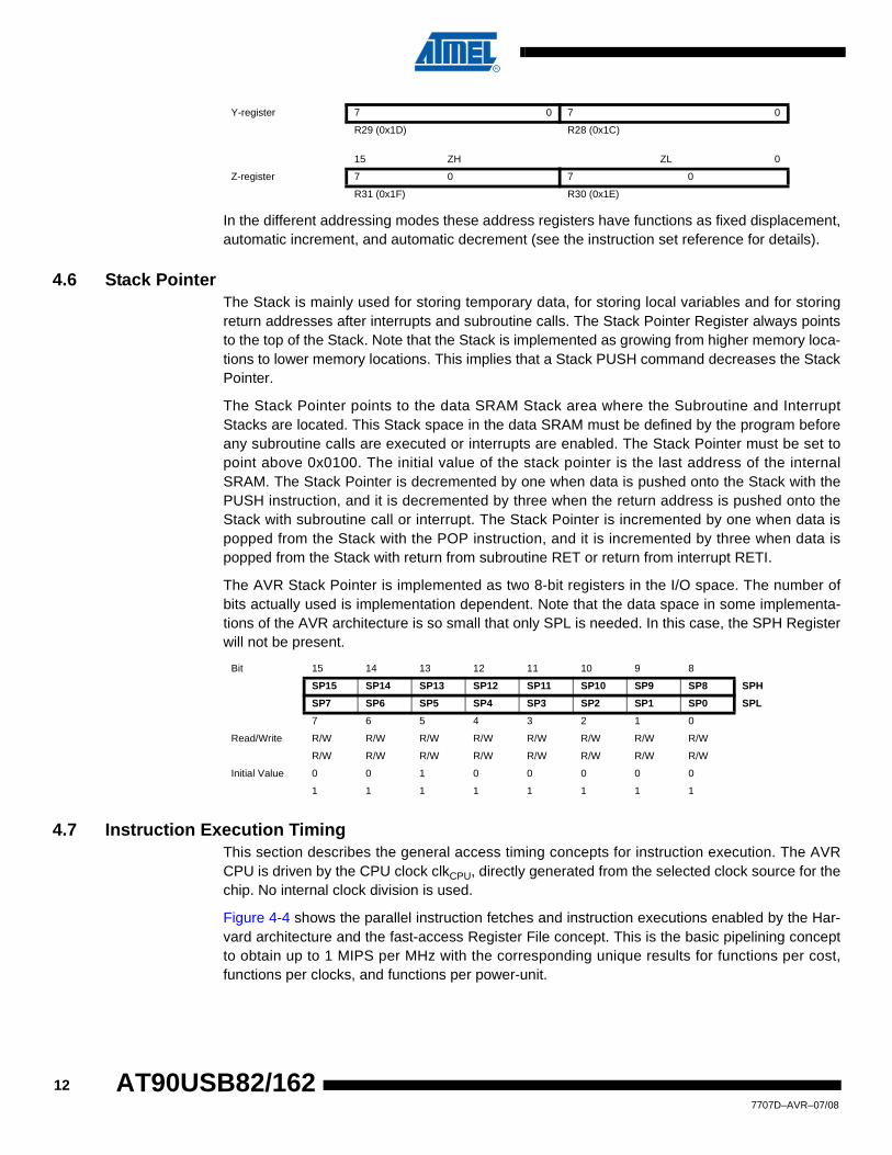
In the different addressing modes these address registers have functions as fixed displacement, automatic increment, and automatic decrement (see the instruction set reference for details).
4.6 Stack PointerThe Stack is mainly used for storing temporary data, for storing local variables and for storing return addresses after interrupts and subroutine calls. The Stack Pointer Register always points to the top of the Stack. Note that the Stack is implemented as growing from higher memory loca-tions to lower memory locations. This implies that a Stack PUSH command decreases the Stack Pointer.
The Stack Pointer points to the data SRAM Stack area where the Subroutine and Interrupt Stacks are located. This Stack space in the data SRAM must be defined by the program before any subroutine calls are executed or interrupts are enabled. The Stack Pointer must be set to point above 0x0100. The initial value of the stack pointer is the last address of the internal SRAM. The Stack Pointer is decremented by one when data is pushed onto the Stack with the PUSH instruction, and it is decremented by three when the return address is pushed onto the Stack with subroutine call or interrupt. The Stack Pointer is incremented by one when data is popped from the Stack with the POP instruction, and it is incremented by three when data is popped from the Stack with return from subroutine RET or return from interrupt RETI.
The AVR Stack Pointer is implemented as two 8-bit registers in the I/O space. The number of bits actually used is implementation dependent. Note that the data space in some implementa-tions of the AVR architecture is so small that only SPL is needed. In this case, the SPH Register will not be present.
4.7 Instruction Execution TimingThis section describes the general access timing concepts for instruction execution. The AVR CPU is driven by the CPU clock clkCPU, directly generated from the selected clock source for the chip. No internal clock division is used.
Figure 4-4 shows the parallel instruction fetches and instruction executions enabled by the Har-vard architecture and the fast-access Register File concept. This is the basic pipelining concept to obtain up to 1 MIPS per MHz with the corresponding unique results for functions per cost, functions per clocks, and functions per power-unit.
Y-register 7 0 7 0
R29 (0x1D) R28 (0x1C)
15 ZH ZL 0
Z-register 7 0 7 0
R31 (0x1F) R30 (0x1E)
Bit 15 14 13 12 11 10 9 8
SP15 SP14 SP13 SP12 SP11 SP10 SP9 SP8 SPH
SP7 SP6 SP5 SP4 SP3 SP2 SP1 SP0 SPL
7 6 5 4 3 2 1 0
Read/Write R/W R/W R/W R/W R/W R/W R/W R/W
R/W R/W R/W R/W R/W R/W R/W R/W
Initial Value 0 0 1 0 0 0 0 0
1 1 1 1 1 1 1 1
127707D–AVR–07/08
AT90USB82/162

AT90USB82/162
Figure 4-4. The Parallel Instruction Fetches and Instruction Executions
Figure 4-5 shows the internal timing concept for the Register File. In a single clock cycle an ALU operation using two register operands is executed, and the result is stored back to the destina-tion register.
Figure 4-5. Single Cycle ALU Operation
4.8 Reset and Interrupt HandlingThe AVR provides several different interrupt sources. These interrupts and the separate Reset Vector each have a separate program vector in the program memory space. All interrupts are assigned individual enable bits which must be written logic one together with the Global Interrupt Enable bit in the Status Register in order to enable the interrupt. Depending on the Program Counter value, interrupts may be automatically disabled when Boot Lock bits BLB02 or BLB12 are programmed. This feature improves software security. See the section “Memory Program-ming” on page 243 for details.
The lowest addresses in the program memory space are by default defined as the Reset and Interrupt Vectors. The complete list of vectors is shown in “Interrupts” on page 63. The list also determines the priority levels of the different interrupts. The lower the address the higher is the priority level. RESET has the highest priority, and next is INT0 – the External Interrupt Request 0. The Interrupt Vectors can be moved to the start of the Boot Flash section by setting the IVSEL bit in the MCU Control Register (MCUCR). Refer to “Interrupts” on page 63 for more information. The Reset Vector can also be moved to the start of the Boot Flash section by programming the BOOTRST Fuse, see “Memory Programming” on page 243.
When an interrupt occurs, the Global Interrupt Enable I-bit is cleared and all interrupts are dis-abled. The user software can write logic one to the I-bit to enable nested interrupts. All enabled interrupts can then interrupt the current interrupt routine. The I-bit is automatically set when a Return from Interrupt instruction – RETI – is executed.
clk
1st Instruction Fetch
1st Instruction Execute2nd Instruction Fetch
2nd Instruction Execute3rd Instruction Fetch
3rd Instruction Execute4th Instruction Fetch
T1 T2 T3 T4
CPU
Total Execution Time
Register Operands Fetch
ALU Operation Execute
Result Write Back
T1 T2 T3 T4
clkCPU
137707D–AVR–07/08
There are basically two types of interrupts. The first type is triggered by an event that sets the Interrupt Flag. For these interrupts, the Program Counter is vectored to the actual Interrupt Vec-tor in order to execute the interrupt handling routine, and hardware clears the corresponding Interrupt Flag. Interrupt Flags can also be cleared by writing a logic one to the flag bit position(s) to be cleared. If an interrupt condition occurs while the corresponding interrupt enable bit is cleared, the Interrupt Flag will be set and remembered until the interrupt is enabled, or the flag is cleared by software. Similarly, if one or more interrupt conditions occur while the Global Interrupt Enable bit is cleared, the corresponding Interrupt Flag(s) will be set and remembered until the Global Interrupt Enable bit is set, and will then be executed by order of priority.
The second type of interrupts will trigger as long as the interrupt condition is present. These interrupts do not necessarily have Interrupt Flags. If the interrupt condition disappears before the interrupt is enabled, the interrupt will not be triggered.
When the AVR exits from an interrupt, it will always return to the main program and execute one more instruction before any pending interrupt is served.
Note that the Status Register is not automatically stored when entering an interrupt routine, nor restored when returning from an interrupt routine. This must be handled by software.
When using the CLI instruction to disable interrupts, the interrupts will be immediately disabled. No interrupt will be executed after the CLI instruction, even if it occurs simultaneously with the CLI instruction. The following example shows how this can be used to avoid interrupts during the timed EEPROM write sequence..
When using the SEI instruction to enable interrupts, the instruction following SEI will be exe-cuted before any pending interrupts, as shown in this example.
Assembly Code Example
in r16, SREG ; store SREG value
cli ; disable interrupts during timed sequence
sbi EECR, EEMPE ; start EEPROM write
sbi EECR, EEPE
out SREG, r16 ; restore SREG value (I-bit)
C Code Example
char cSREG;
cSREG = SREG; /* store SREG value */
/* disable interrupts during timed sequence */
__disable_interrupt();
EECR |= (1<<EEMPE); /* start EEPROM write */
EECR |= (1<<EEPE);
SREG = cSREG; /* restore SREG value (I-bit) */
147707D–AVR–07/08
AT90USB82/162

AT90USB82/162
4.8.1 Interrupt Response TimeThe interrupt execution response for all the enabled AVR interrupts is five clock cycles minimum. After five clock cycles the program vector address for the actual interrupt handling routine is exe-cuted. During these five clock cycle period, the Program Counter is pushed onto the Stack. The vector is normally a jump to the interrupt routine, and this jump takes three clock cycles. If an interrupt occurs during execution of a multi-cycle instruction, this instruction is completed before the interrupt is served. If an interrupt occurs when the MCU is in sleep mode, the interrupt exe-cution response time is increased by five clock cycles. This increase comes in addition to the start-up time from the selected sleep mode.
A return from an interrupt handling routine takes three clock cycles. During these three clock cycles, the Program Counter (three bytes) is popped back from the Stack, the Stack Pointer is incremented by three, and the I-bit in SREG is set.
Assembly Code Example
sei ; set Global Interrupt Enable
sleep; enter sleep, waiting for interrupt
; note: will enter sleep before any pending
; interrupt(s)
C Code Example
__enable_interrupt(); /* set Global Interrupt Enable */
__sleep(); /* enter sleep, waiting for interrupt */
/* note: will enter sleep before any pending interrupt(s) */
157707D–AVR–07/08

5. AVR AT90USB82/162 MemoriesThis section describes the different memories in the AT90USB82/162. The AVR architecture has two main memory spaces, the Data Memory and the Program Memory space. In addition, the AT90USB82/162 features an EEPROM Memory for data storage. All three memory spaces are linear and regular.
5.1 In-System Reprogrammable Flash Program Memory The AT90USB82/162 contains 8K / 16K bytes On-chip In-System Reprogrammable Flash mem-ory for program storage. Since all AVR instructions are 16 or 32 bits wide, the Flash is organized as 4K x 16, 8K x 16. For software security, the Flash Program memory space is divided into two sections, Boot Program section and Application Program section.
The Flash memory has an endurance of at least 100,000 write/erase cycles. The AT90USB82/162 Program Counter (PC) is 16 bits wide, thus addressing the 8K / 16K program memory locations. The operation of Boot Program section and associated Boot Lock bits for software protection are described in detail in “Memory Programming” on page 243. “Memory Programming” on page 243 contains a detailed description on Flash data serial downloading using the SPI pins or the debugWIRE interface.
Constant tables can be allocated within the entire program memory address space (see the LPM – Load Program Memory instruction description and ELPM - Extended Load Program Memory instruction description).
Timing diagrams for instruction fetch and execution are presented in “Instruction Execution Tim-ing” on page 12.
167707D–AVR–07/08
AT90USB82/162

AT90USB82/162
Figure 5-1. Program Memory Map
5.2 SRAM Data MemoryFigure 5-2 shows how the AT90USB82/162 SRAM Memory is organized.
The AT90USB82/162 is a complex microcontroller with more peripheral units than can be sup-ported within the 64 location reserved in the Opcode for the IN and OUT instructions. For the Extended I/O space from $060 - $0FF in SRAM, only the ST/STS/STD and LD/LDS/LDD instruc-tions can be used.
The first 768 Data Memory locations address the Register File, the I/O Memory, Extended I/O Memory, and the internal data SRAM. The first 32 locations address the Register file, the next 64 location the standard I/O Memory, then 160 locations of Extended I/O memory, and the 512 locations of internal data SRAM.The five different addressing modes for the data memory cover: Direct, Indirect with Displacement, Indirect, Indirect with Pre-decrement, and Indirect with Post-increment. In the Register file, registers R26 to R31 feature the indirect addressing pointer registers.
The direct addressing reaches the entire data space.
The Indirect with Displacement mode reaches 63 address locations from the base address given by the Y- or Z-register.
When using register indirect addressing modes with automatic pre-decrement and post-incre-ment, the address registers X, Y, and Z are decremented or incremented.
0x00000
0x1FFF (8KBytes)0x3FFF (16KBytes)
Program Memory
Application Flash Section
Boot Flash Section
177707D–AVR–07/08
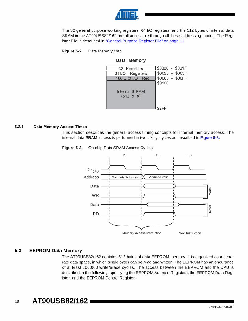
The 32 general purpose working registers, 64 I/O registers, and the 512 bytes of internal data SRAM in the AT90USB82/162 are all accessible through all these addressing modes. The Reg-ister File is described in “General Purpose Register File” on page 11.
Figure 5-2. Data Memory Map
5.2.1 Data Memory Access TimesThis section describes the general access timing concepts for internal memory access. The internal data SRAM access is performed in two clkCPU cycles as described in Figure 5-3.
Figure 5-3. On-chip Data SRAM Access Cycles
5.3 EEPROM Data MemoryThe AT90USB82/162 contains 512 bytes of data EEPROM memory. It is organized as a sepa-rate data space, in which single bytes can be read and written. The EEPROM has an endurance of at least 100,000 write/erase cycles. The access between the EEPROM and the CPU is described in the following, specifying the EEPROM Address Registers, the EEPROM Data Reg-ister, and the EEPROM Control Register.
32 Registers64 I/O Registers
Internal S RAM(512 x 8)
$0000 - $001F$0020 - $005F
$2FF
$0060 - $00FF
Data Memory
160 E xt I/O Reg.$0100
clk
WR
RD
Data
Data
Address Address valid
T1 T2 T3
Compute Address
Rea
dW
rite
CPU
Memory Access Instruction Next Instruction
187707D–AVR–07/08
AT90USB82/162

AT90USB82/162
For a detailed description of SPI, debugWIRE and Parallel data downloading to the EEPROM, see page 257, page 241, and page 246 respectively.
5.3.1 EEPROM Read/Write AccessThe EEPROM Access Registers are accessible in the I/O space.
The write access time for the EEPROM is given in Table 5-2. A self-timing function, however, lets the user software detect when the next byte can be written. If the user code contains instruc-tions that write the EEPROM, some precautions must be taken. In heavily filtered power supplies, VCC is likely to rise or fall slowly on power-up/down. This causes the device for some period of time to run at a voltage lower than specified as minimum for the clock frequency used. See “Preventing EEPROM Corruption” on page 23. for details on how to avoid problems in these situations.
In order to prevent unintentional EEPROM writes, a specific write procedure must be followed. Refer to the description of the EEPROM Control Register for details on this.
When the EEPROM is read, the CPU is halted for four clock cycles before the next instruction is executed. When the EEPROM is written, the CPU is halted for two clock cycles before the next instruction is executed.
5.3.2 The EEPROM Address Register – EEARH and EEARL
• Bits 15..12 – Res: Reserved BitsThese bits are reserved bits in the AT90USB82/162 and will always read as zero.
• Bits 11..0 – EEAR8..0: EEPROM AddressThe EEPROM Address Registers – EEARH and EEARL specify the EEPROM address in the 512 bytes EEPROM space. The EEPROM data bytes are addressed linearly between 0 and 512. The initial value of EEAR is undefined. A proper value must be written before the EEPROM may be accessed.
5.3.3 The EEPROM Data Register – EEDR
• Bits 7..0 – EEDR7.0: EEPROM DataFor the EEPROM write operation, the EEDR Register contains the data to be written to the EEPROM in the address given by the EEAR Register. For the EEPROM read operation, the EEDR contains the data read out from the EEPROM at the address given by EEAR.
Bit 15 14 13 12 11 10 9 8
– – – – EEAR11 EEAR10 EEAR9 EEAR8 EEARH
EEAR7 EEAR6 EEAR5 EEAR4 EEAR3 EEAR2 EEAR1 EEAR0 EEARL
7 6 5 4 3 2 1 0
Read/Write R R R R R/W R/W R/W R/W
R/W R/W R/W R/W R/W R/W R/W R/W
Initial Value 0 0 0 0 X X X X
X X X X X X X X
Bit 7 6 5 4 3 2 1 0
MSB LSB EEDR
Read/Write R/W R/W R/W R/W R/W R/W R/W R/W
Initial Value 0 0 0 0 0 0 0 0
197707D–AVR–07/08

5.3.4 The EEPROM Control Register – EECR
• Bits 7..6 – Res: Reserved BitsThese bits are reserved bits in the AT90USB82/162 and will always read as zero.
• Bits 5, 4 – EEPM1 and EEPM0: EEPROM Programming Mode BitsThe EEPROM Programming mode bit setting defines which programming action that will be trig-gered when writing EEPE. It is possible to program data in one atomic operation (erase the old value and program the new value) or to split the Erase and Write operations in two different operations. The Programming times for the different modes are shown in Table 5-1. While EEPE is set, any write to EEPMn will be ignored. During reset, the EEPMn bits will be reset to 0b00 unless the EEPROM is busy programming.
• Bit 3 – EERIE: EEPROM Ready Interrupt EnableWriting EERIE to one enables the EEPROM Ready Interrupt if the I bit in SREG is set. Writing EERIE to zero disables the interrupt. The EEPROM Ready interrupt generates a constant inter-rupt when EEPE is cleared.
• Bit 2 – EEMPE: EEPROM Master Programming EnableThe EEMPE bit determines whether setting EEPE to one causes the EEPROM to be written. When EEMPE is set, setting EEPE within four clock cycles will write data to the EEPROM at the selected address If EEMPE is zero, setting EEPE will have no effect. When EEMPE has been written to one by software, hardware clears the bit to zero after four clock cycles. See the description of the EEPE bit for an EEPROM write procedure.
• Bit 1 – EEPE: EEPROM Programming EnableThe EEPROM Write Enable Signal EEPE is the write strobe to the EEPROM. When address and data are correctly set up, the EEPE bit must be written to one to write the value into the EEPROM. The EEMPE bit must be written to one before a logical one is written to EEPE, other-wise no EEPROM write takes place. The following procedure should be followed when writing the EEPROM (the order of steps 3 and 4 is not essential):
1. Wait until EEPE becomes zero.
2. Wait until SELFPRGEN in SPMCSR becomes zero.
3. Write new EEPROM address to EEAR (optional).
Bit 7 6 5 4 3 2 1 0
– – EEPM1 EEPM0 EERIE EEMPE EEPE EERE EECR
Read/Write R R R/W R/W R/W R/W R/W R/W
Initial Value 0 0 X X 0 0 X 0
Table 5-1. EEPROM Mode Bits
EEPM1 EEPM0Programming
Time Operation
0 0 3.4 ms Erase and Write in one operation (Atomic Operation)
0 1 1.8 ms Erase Only
1 0 1.8 ms Write Only
1 1 – Reserved for future use
207707D–AVR–07/08
AT90USB82/162

AT90USB82/162
4. Write new EEPROM data to EEDR (optional).
5. Write a logical one to the EEMPE bit while writing a zero to EEPE in EECR.
6. Within four clock cycles after setting EEMPE, write a logical one to EEPE.
The EEPROM can not be programmed during a CPU write to the Flash memory. The software must check that the Flash programming is completed before initiating a new EEPROM write. Step 2 is only relevant if the software contains a Boot Loader allowing the CPU to program the Flash. If the Flash is never being updated by the CPU, step 2 can be omitted. See “Memory Pro-gramming” on page 243 for details about Boot programming.
Caution: An interrupt between step 5 and step 6 will make the write cycle fail, since the EEPROM Master Write Enable will time-out. If an interrupt routine accessing the EEPROM is interrupting another EEPROM access, the EEAR or EEDR Register will be modified, causing the interrupted EEPROM access to fail. It is recommended to have the Global Interrupt Flag cleared during all the steps to avoid these problems.
When the write access time has elapsed, the EEPE bit is cleared by hardware. The user soft-ware can poll this bit and wait for a zero before writing the next byte. When EEPE has been set, the CPU is halted for two cycles before the next instruction is executed.
• Bit 0 – EERE: EEPROM Read EnableThe EEPROM Read Enable Signal EERE is the read strobe to the EEPROM. When the correct address is set up in the EEAR Register, the EERE bit must be written to a logic one to trigger the EEPROM read. The EEPROM read access takes one instruction, and the requested data is available immediately. When the EEPROM is read, the CPU is halted for four cycles before the next instruction is executed.
The user should poll the EEPE bit before starting the read operation. If a write operation is in progress, it is neither possible to read the EEPROM, nor to change the EEAR Register.
The calibrated Oscillator is used to time the EEPROM accesses. Table 5-2 lists the typical pro-gramming time for EEPROM access from the CPU.
The following code examples show one assembly and one C function for writing to the EEPROM. The examples assume that interrupts are controlled (e.g. by disabling interrupts glo-bally) so that no interrupts will occur during execution of these functions. The examples also
Table 5-2. EEPROM Programming Time
Symbol Number of Calibrated RC Oscillator Cycles Typ Programming Time
EEPROM write (from CPU)
26,368 3.3 ms
217707D–AVR–07/08

assume that no Flash Boot Loader is present in the software. If such code is present, the EEPROM write function must also wait for any ongoing SPM command to finish.
Note: 1. See “About Code Examples” on page 7.
Assembly Code Example(1)
EEPROM_write:
; Wait for completion of previous write
sbic EECR,EEPE
rjmp EEPROM_write
; Set up address (r18:r17) in address register
out EEARH, r18
out EEARL, r17
; Write data (r16) to Data Register
out EEDR,r16
; Write logical one to EEMPE
sbi EECR,EEMPE
; Start eeprom write by setting EEPE
sbi EECR,EEPE
ret
C Code Example(1)
void EEPROM_write(unsigned int uiAddress, unsigned char ucData)
{
/* Wait for completion of previous write */
while(EECR & (1<<EEPE))
;
/* Set up address and Data Registers */
EEAR = uiAddress;
EEDR = ucData;
/* Write logical one to EEMPE */
EECR |= (1<<EEMPE);
/* Start eeprom write by setting EEPE */
EECR |= (1<<EEPE);
}
227707D–AVR–07/08
AT90USB82/162

AT90USB82/162
The next code examples show assembly and C functions for reading the EEPROM. The exam-ples assume that interrupts are controlled so that no interrupts will occur during execution of these functions.
Note: 1. See “About Code Examples” on page 7.
5.3.5 Preventing EEPROM CorruptionDuring periods of low VCC, the EEPROM data can be corrupted because the supply voltage is too low for the CPU and the EEPROM to operate properly. These issues are the same as for board level systems using EEPROM, and the same design solutions should be applied.
An EEPROM data corruption can be caused by two situations when the voltage is too low. First, a regular write sequence to the EEPROM requires a minimum voltage to operate correctly. Sec-ondly, the CPU itself can execute instructions incorrectly, if the supply voltage is too low.
EEPROM data corruption can easily be avoided by following this design recommendation:
Keep the AVR RESET active (low) during periods of insufficient power supply voltage. This can be done by enabling the internal Brown-out Detector (BOD). If the detection level of the internal BOD does not match the needed detection level, an external low VCC reset Protection circuit can
Assembly Code Example(1)
EEPROM_read:
; Wait for completion of previous write
sbic EECR,EEPE
rjmp EEPROM_read
; Set up address (r18:r17) in address register
out EEARH, r18
out EEARL, r17
; Start eeprom read by writing EERE
sbi EECR,EERE
; Read data from Data Register
in r16,EEDR
ret
C Code Example(1)
unsigned char EEPROM_read(unsigned int uiAddress)
{
/* Wait for completion of previous write */
while(EECR & (1<<EEPE))
;
/* Set up address register */
EEAR = uiAddress;
/* Start eeprom read by writing EERE */
EECR |= (1<<EERE);
/* Return data from Data Register */
return EEDR;
}
237707D–AVR–07/08

be used. If a reset occurs while a write operation is in progress, the write operation will be com-pleted provided that the power supply voltage is sufficient.
5.4 I/O MemoryThe I/O space definition of the AT90USB82/162 is shown in “Register Summary” on page 288.
All AT90USB82/162 I/Os and peripherals are placed in the I/O space. All I/O locations may be accessed by the LD/LDS/LDD and ST/STS/STD instructions, transferring data between the 32 general purpose working registers and the I/O space. I/O Registers within the address range 0x00 - 0x1F are directly bit-accessible using the SBI and CBI instructions. In these registers, the value of single bits can be checked by using the SBIS and SBIC instructions. Refer to the instruction set section for more details. When using the I/O specific commands IN and OUT, the I/O addresses 0x00 - 0x3F must be used. When addressing I/O Registers as data space using LD and ST instructions, 0x20 must be added to these addresses. The AT90USB82/162 is a complex microcontroller with more peripheral units than can be supported within the 64 location reserved in Opcode for the IN and OUT instructions. For the Extended I/O space from 0x60 - 0x1FF in SRAM, only the ST/STS/STD and LD/LDS/LDD instructions can be used.
For compatibility with future devices, reserved bits should be written to zero if accessed. Reserved I/O memory addresses should never be written.
Some of the Status Flags are cleared by writing a logical one to them. Note that, unlike most other AVRs, the CBI and SBI instructions will only operate on the specified bit, and can therefore be used on registers containing such Status Flags. The CBI and SBI instructions work with reg-isters 0x00 to 0x1F only.
The I/O and peripherals control registers are explained in later sections.
5.4.1 General Purpose I/O RegistersThe AT90USB82/162 contains three General Purpose I/O Registers. These registers can be used for storing any information, and they are particularly useful for storing global variables and Status Flags. General Purpose I/O Registers within the address range 0x00 - 0x1F are directly bit-accessible using the SBI, CBI, SBIS, and SBIC instructions.
5.4.2 General Purpose I/O Register 2 – GPIOR2
5.4.3 General Purpose I/O Register 1 – GPIOR1
5.4.4 General Purpose I/O Register 0 – GPIOR0
Bit 7 6 5 4 3 2 1 0
MSB LSB GPIOR2
Read/Write R/W R/W R/W R/W R/W R/W R/W R/W
Initial Value 0 0 0 0 0 0 0 0
Bit 7 6 5 4 3 2 1 0
MSB LSB GPIOR1
Read/Write R/W R/W R/W R/W R/W R/W R/W R/W
Initial Value 0 0 0 0 0 0 0 0
Bit 7 6 5 4 3 2 1 0
MSB LSB GPIOR0
Read/Write R/W R/W R/W R/W R/W R/W R/W R/W
Initial Value 0 0 0 0 0 0 0 0
247707D–AVR–07/08
AT90USB82/162

AT90USB82/162
6. System Clock and Clock Options
6.1 Clock Systems and their DistributionFigure 6-1 presents the principal clock systems in the AVR and their distribution. All of the clocks need not be active at a given time. In order to reduce power consumption, the clocks to modules not being used can be halted by using different sleep modes, as described in “Power Manage-ment and Sleep Modes” on page 41. The clock systems are detailed below.
Figure 6-1. Clock Distribution
6.1.1 CPU Clock – clkCPU
The CPU clock is routed to parts of the system concerned with operation of the AVR core. Examples of such modules are the General Purpose Register File, the Status Register and the data memory holding the Stack Pointer. Halting the CPU clock inhibits the core from performing general operations and calculations.
6.1.2 I/O Clock – clkI/O
The I/O clock is used by the majority of the I/O modules, like Timer/Counters, SPI, and USART. The I/O clock is also used by the External Interrupt module, but note that some external inter-rupts are detected by asynchronous logic, allowing such interrupts to be detected even if the I/O clock is halted.
6.1.3 Flash Clock – clkFLASH
The Flash clock controls operation of the Flash interface. The Flash clock is usually active simul-taneously with the CPU clock.
General I/OModules
CPU Core RAM
clkI/O AVR ClockControl Unit
clkCPU
Flash andEEPROM
clkFLASH
Source clock
Watchdog TimerReset Logic
ClockMultiplexer
Watchdog clock
Calibrated RCOscillator
CrystalOscillator
External Clock
System ClockPrescaler
ClockSwitch
WatchdogOscillator
USB
clkUSB (48MHz)
PLL ClockPrescaler
clkPllin (8MHz)
USB PLLX6
clkXTAL (2-16 MHz)
257707D–AVR–07/08

6.1.4 USB Clock – clkUSB
The USB is provided with a dedicated clock domain. This clock is generated with an on-chip PLL running at 48MHz. The PLL always multiply its input frequency by 6. Thus the PLL clock register should be programmed by software to generate a 8MHz clock on the PLL input.
6.2 Clock SwitchIn the AT90USB82/162 product, the Clock Multiplexer and the System Clock Prescaler can be modified by software.
6.2.1 Exemple of useThe modification can occur when the device enters in USB Suspend mode. It then switches from External Clock to Calibrated RC Oscillator in order to reduce consumption. In such a configura-tion, the External Clock is disabled.
The firmware can use the watchdog timer to be woken-up from power-down in order to check if there is an event on the application.
If an event occurs on the application or if the USB controller signals a non-idle state on the USB line (Resume for example), the firmware switches the Clock Multiplexer from the Calibrated RC Oscillator to the External Clock.
Figure 6-2. Example of clock switching with wake-up from USB Host
USB
CPU Clock
ExternalOscillator
RC oscillator
Ext RC Ext
non-Idle Idle (Suspend) non-Idle
3ms
resume
1
1 Resume from Host
watchdog wake-upfrom power-down
267707D–AVR–07/08
AT90USB82/162

AT90USB82/162
Figure 6-3. Example of clock switching with wake-up from Device
6.2.2 Clock switch Algorythm
6.2.2.1 Swith from external clock to RC clockif (Usb_suspend_detected()) // if (UDINT.SUSPI == 1)
{
Usb_ack_suspend(); // UDINT.SUSPI = 0;
Usb_freeze_clock(); // USBCON.FRZCLK = 1;
Disable_pll(); // PLLCSR.PLLE = 0;
Enable_RC_clock(); // CLKSEL0.RCE = 1;
while (!RC_clock_ready()); // while (CLKSTA.RCON != 1);
Select_RC_clock(); // CLKSEL0.CLKS = 0;
Disable_external_clock(); // CLKSEL0.EXTE = 0;
}
6.2.2.2 Switch from RC clock to external clockif (Usb_wake_up_detected()) // if (UDINT.WAKEUPI == 1)
{
Usb_ack_wake_up(); // UDINT.WAKEUPI = 0;
Enable_external_clock(); // CLKSEL0.EXTE = 1;
while (!External_clock_ready()); // while (CLKSTA.EXTON != 1);
Select_external_clock(); // CLKSEL0.CLKS = 1;
Enable_pll(); // PLLCSR.PLLE = 1;
Disable_RC_clock(); // CLKSEL0.RCE = 0;
while (!Pll_ready()); // while (PLLCSR.PLOCK != 1);
Usb_unfreeze_clock(); // USBCON.FRZCLK = 0;
}
6.2.3 Clock Selection Register 0 – CLKSEL0
USB
CPU Clock
ExternalOscillator
RC oscillator
Ext RC Ext
non-Idle Idle (Suspend) non-Idle
3ms
upstream-resume
2
2 Upstream Resume from device
watchdog wake-upfrom power-down
Bit 7 6 5 4 3 2 1 0
RCSUT1 RCSUT0 EXSUT1 EXSUT0 RCE EXTE - CLKS CLKSEL0
Read/Write R/W R/W R/W R/W R/W R/W R R/W
Initial Value 0 0 0 0 See Bit Description
277707D–AVR–07/08

• Bit 7-6 – RCSUT[1:0]: SUT for RC oscillatorThese 2 bits are the SUT value for the RC Oscillator. If the RC oscillator is selected by fuse bits, the SUT fuse are copied into these bits. A firmware change will not have any effect because this additionnal start-up time is only used after a reset and not after a clock switch.
• Bit 5-4 – EXSUT[1:0]: SUT for External Oscillator / Low Power OscillatorThese 2 bits are the SUT value for the External Oscillator / Low Power Oscillator. If the External oscillator / Low Power Oscillator is selected by fuse bits, the SUT fuse are copyed into these bits. The firmware can modify these bits by writing a new value. This value will be used at the next start of the External Oscillator / Low Power Oscillator.
• Bit 3 – RCE: Enable RC OscillatorThe RCE bit must be written to logic one to enable the RC Oscillator. The RCE bit must be writ-ten to logic zero to disable the RC Oscillator.
• Bit 2 – EXTE: Enable External Oscillator / Low Power OscillatorThe OSCE bit must be written to logic one to enable External Oscillator / Low Power Oscillator. The OSCE bit must be written to logic zero to disable the External Oscillator / Low Power Oscillator.
• Bit 0 – CLKS: Clock SelectorThe CLKS bit must be written to logic one to select the External Oscillator / Low Power Oscillator as CPU clock. The CLKS bit must be written to logic zero to select the RC Oscillator as CPU clock. After a reset, the CLKS bit is set by hardware if the External Oscillator / Low Power Oscil-lator is selected by the fuse bits configuration. The firmware has to check if the clock is correctly started before selected it.
6.2.4 Clock Selection Register 1 – CLKSEL1
• Bit 7-4 – RCCKSEL[3:0]: CKSEL for RC oscillatorClock configuration for the RC Oscillator. After a reset, this part of the register is loaded with the 0010b value that corresponds to the RC oscillator. Modifying this value by firmware before switching to RC oscillator is prohibited because the RC clock will not start.
• Bit 3-0 – EXCKSEL[3:0]: CKSEL for External oscillator / Low Power OscillatorClock configuration for the External Oscillator / Low Power Oscillator. After a reset, if the Exter-nal oscillator / Low Power Oscillator is selected by fuse bits, this part of the register is loaded with the fuse configuration. Firmware can modify it to change the start-up time after the clock switch.
Bit 7 6 5 4 3 2 1 0
RCCKSEL3
RCCKSEL2
RCCLKSEL1
RCCLKSEL0
EXCKSEL3
EXCKSEL2
EXCLKSEL1
EXCLKSEL0
CLKSEL1
Read/Write R/W R/W R/W R/W R/W R/W R/W R/W
Initial Value 0 0 1 0 0 0 0 0
287707D–AVR–07/08
AT90USB82/162

AT90USB82/162
6.2.5 Clock Status Register – CLKSTA
• Bit 7-2 - Reserved bitsThese bits are reserved and will always read as zero.
• Bit 1 – RCON: RC Oscillator OnThis bit is set by hardware to one if the RC Oscillator is running. This bit is set by hardware to zero if the RC Oscillator is stoped.
• Bit 0 – EXTON: External Oscillator / Low Power Oscillator OnThis bit is set by hardware to one if the External Oscillator / Low Power Oscillator is running. This bit is set by hardware to zero if the External Oscillator / Low Power Oscillator is stoped.
6.3 Clock SourcesThe device has the following clock source options, selectable by Flash Fuse bits as shown below. The clock from the selected source is input to the AVR clock generator, and routed to the appropriate modules.
Note: 1. For all fuses “1” means unprogrammed while “0” means programmed.
6.3.1 Default Clock SourceThe device is shipped with internal RC oscillator at 8.0 MHz and with the fuse CKDIV8 pro-grammed, resulting in 1.0 MHz system clock. The startup time is set to maximum and time-out period enabled. (CKSEL = "0010", SUT = "10", CKDIV8 = "0"). The default setting ensures that all users can make their desired clock source setting using any available programming interface.
6.3.2 Clock Startup SequenceAny clock source needs a sufficient VCC to start oscillating and a minimum number of oscillating cycles before it can be considered stable.
To ensure sufficient VCC, the device issues an internal reset with a time-out delay (tTOUT) after the device reset is released by all other reset sources. “On-chip Debug System” on page 45describes the start conditions for the internal reset. The delay (tTOUT) is timed from the Watchdog Oscillator and the number of cycles in the delay is set by the SUTx and CKSELx fuse bits. The
Bit 7 6 5 4 3 2 1 0
- - - - - - RCON EXTON CLKSTA
Read/Write R R R R R R R R
Initial Value 0 0 0 0 See Bit Description
Table 6-1. Device Clocking Options Select(1)
Device Clocking Option CKSEL3..0
Low Power Crystal Oscillator 1111 - 1000
Reserved 0111 - 0110
Reserved 0101 - 0100
Reserved 0011
Calibrated Internal RC Oscillator 0010
External Clock 0000
Reserved 0001
297707D–AVR–07/08
selectable delays are shown in Table 6-2. The frequency of the Watchdog Oscillator is voltage dependent as shown in “AT90USB82/162 Typical Characteristics – Preliminary Data” on page 268.
Main purpose of the delay is to keep the AVR in reset until it is supplied with minimum Vcc. The delay will not monitor the actual voltage and it will be required to select a delay longer than the Vcc rise time. If this is not possible, an internal or external Brown-Out Detection circuit should be used. A BOD circuit will ensure sufficient Vcc before it releases the reset, and the time-out delay can be disabled. Disabling the time-out delay without utilizing a Brown-Out Detection circuit is not recommended.
The oscillator is required to oscillate for a minimum number of cycles before the clock is consid-ered stable. An internal ripple counter monitors the oscillator output clock, and keeps the internal reset active for a given number of clock cycles. The reset is then released and the device will start to execute. The recommended oscillator start-up time is dependent on the clock type, and varies from 6 cycles for an externally applied clock to 32K cycles for a low frequency crystal.
The start-up sequence for the clock includes both the time-out delay and the start-up time when the device starts up from reset. When starting up from Power-save or Power-down mode, Vcc is assumed to be at a sufficient level and only the start-up time is included.
6.4 Low Power Crystal OscillatorPins XTAL1 and XTAL2 are input and output, respectively, of an inverting amplifier which can be configured for use as an On-chip Oscillator, as shown in Figure 6-4. Either a quartz crystal or a ceramic resonator may be used.
This Crystal Oscillator is a low power oscillator, with reduced voltage swing on the XTAL2 out-put. It gives the lowest power consumption, but is not capable of driving other clock inputs, and may be more susceptible to noise in noisy environments.
C1 and C2 should always be equal for both crystals and resonators. The optimal value of the capacitors depends on the crystal or resonator in use, the amount of stray capacitance, and the electromagnetic noise of the environment. Some initial guidelines for choosing capacitors for use with crystals are given in Table 6-3. For ceramic resonators, the capacitor values given by the manufacturer should be used.
Table 6-2. Number of Watchdog Oscillator Cycles
Typ Time-out (VCC = 5.0V) Typ Time-out (VCC = 3.0V) Number of Cycles
0 ms 0 ms 0
4.1 ms 4.3 ms 512
65 ms 69 ms 8K (8,192)
307707D–AVR–07/08
AT90USB82/162

AT90USB82/162
Figure 6-4. Crystal Oscillator Connections
The Low Power Oscillator can operate in three different modes, each optimized for a specific fre-quency range. The operating mode is selected by the fuses CKSEL3..1 as shown in Table 6-3.
Notes: 1. The frequency ranges are preliminary values. Actual values are TBD.
2. This option should not be used with crystals, only with ceramic resonators.
3. If 8 MHz frequency exceeds the specification of the device (depends on VCC), the CKDIV8 Fuse can be programmed in order to divide the internal frequency by 8. It must be ensured that the resulting divided clock meets the frequency specification of the device.
The CLKSEL0 Fuse together with the SUT1..0 Fuses select the start-up times as shown in Table 6-4.
Table 6-3. Low Power Crystal Oscillator Operating Modes(3)
Frequency Range(1) (MHz) CKSEL3..1Recommended Range for Capacitors C1
and C2 (pF)
0.4 - 0.9 100(2) –
0.9 - 3.0 101 12 - 22
3.0 - 8.0 110 12 - 22
8.0 - 16.0 111 12 - 22
Table 6-4. Start-up Times for the Low Power Crystal Oscillator Clock Selection
Oscillator Source / Power Conditions
Start-up Time from Power-down and
Power-save
Additional Delay from Reset (VCC = 5.0V)
CLKSEL0 SUT1..0
Ceramic resonator, fast rising power
258 CK 14CK + 4.1 ms(1) 0 00
Ceramic resonator, slowly rising power
258 CK 14CK + 65 ms(1) 0 01
Ceramic resonator, BOD enabled
1K CK 14CK(2) 0 10
Ceramic resonator, fast rising power
1K CK 14CK + 4.1 ms(2) 0 11
Ceramic resonator, slowly rising power
1K CK 14CK + 65 ms(2) 1 00
XTAL2
XTAL1
GND
C2
C1
317707D–AVR–07/08

Notes: 1. These options should only be used when not operating close to the maximum frequency of the device, and only if frequency stability at start-up is not important for the application. These options are not suitable for crystals.
2. These options are intended for use with ceramic resonators and will ensure frequency stability at start-up. They can also be used with crystals when not operating close to the maximum fre-quency of the device, and if frequency stability at start-up is not important for the application.
Note: 1. The device is shipped with this option selected.
6.5 Calibrated Internal RC OscillatorThe calibrated internal RC Oscillator by default provides a 8.0 MHz clock. The fre-quency is nominal value at 3.0V and 25°C. At 3.0V and 25°C, this calibration gives a frequency of 8 MHz ± 10%. The device is shipped with the CKDIV8 Fuse programmed. See “System Clock Prescaler” on page 34 for more details. This clock may be selected as the system clock by programming the CKSEL Fuses as shown in Table 6-6. If selected, it will operate with no external components. During reset, hardware loads the calibration byte into the OSCCAL Register and thereby automatically calibrates the RC Oscillator. At 3.3V and 25°C, this calibration gives a frequency of 8 MHz ± 1%. The oscillator can be calibrated to any frequency in the range 7.3 - 8.1 MHz within ±1% accuracy, by changing the OSCCAL register. When this Oscillator is used as the chip clock, the Watchdog Oscillator will still be used for the Watchdog Timer and for the Reset Time-out. For more information on the pre-programmed calibration value, see the section “Calibration Byte” on page 246
Notes: 1. The device is shipped with this option selected.
2. The frequency ranges are preliminary values. Actual values are TBD.
Crystal Oscillator, BOD enabled
16K CK 14CK 1 01
Crystal Oscillator, fast rising power
16K CK 14CK + 4.1 ms 1 10
Crystal Oscillator, slowly rising power
16K CK 14CK + 65 ms 1 11
Table 6-5. Start-up times for the internal calibrated RC Oscillator clock selection
Power ConditionsStart-up Time from Power-
down and Power-saveAdditional Delay from
Reset (VCC = 5.0V) SUT1..0
BOD enabled 6 CK 14CK 00
Fast rising power 6 CK 14CK + 4.1 ms 01
Slowly rising power 6 CK 14CK + 65 ms(1) 10
Reserved 11
Table 6-4. Start-up Times for the Low Power Crystal Oscillator Clock Selection (Continued)
Oscillator Source / Power Conditions
Start-up Time from Power-down and
Power-save
Additional Delay from Reset (VCC = 5.0V)
CLKSEL0 SUT1..0
Table 6-6. Internal Calibrated RC Oscillator Operating Modes(1)(3)
Frequency Range(2) (MHz) CKSEL3..0
7.3 - 8.1 0010
327707D–AVR–07/08
AT90USB82/162

AT90USB82/162
3. If 8 MHz frequency exceeds the specification of the device (depends on VCC), the CKDIV8 Fuse can be programmed in order to divide the internal frequency by 8.
When this Oscillator is selected, start-up times are determined by the SUT Fuses as shown in Table 6-5 on page 32.
Note: 1. The device is shipped with this option selected.
6.5.1 Oscillator Calibration Register – OSCCAL
• Bits 7..0 – CAL7..0: Oscillator Calibration ValueThe Oscillator Calibration Register is used to trim the Calibrated Internal RC Oscillator to remove process variations from the oscillator frequency. The factory-calibrated value is automat-ically written to this register during chip reset, giving an oscillator frequency of 8.0 MHz at 25°C. The application software can write this register to change the oscillator frequency. The oscillator can be calibrated to any frequency in the range 7.3 - 8.1 MHz within ±1% accuracy. Calibration outside that range is not guaranteed.
Note that this oscillator is used to time EEPROM and Flash write accesses, and these write times will be affected accordingly. If the EEPROM or Flash are written, do not calibrate to more than 8.8 MHz. Otherwise, the EEPROM or Flash write may fail.
The CAL7 bit determines the range of operation for the oscillator. Setting this bit to 0 gives the lowest frequency range, setting this bit to 1 gives the highest frequency range. The two fre-quency ranges are overlapping, in other words a setting of OSCCAL = 0x7F gives a higher frequency than OSCCAL = 0x80.
The CAL6..0 bits are used to tune the frequency within the selected range. A setting of 0x00 gives the lowest frequency in that range, and a setting of 0x7F gives the highest frequency in the range. Incrementing CAL6..0 by 1 will give a frequency increment of less than 2% in the fre-quency range 7.3 - 8.1 MHz.
Table 6-7. Start-up times for the internal calibrated RC Oscillator clock selection
Power ConditionsStart-up Time from Power-
down and Power-saveAdditional Delay from
Reset (VCC = 5.0V) SUT1..0
BOD enabled 6 CK 14 CK 00
Fast rising power 6 CK 14 CK + 4.1 ms 01
Slowly rising power 6 CK 14 CK + 65 ms(1) 10
Reserved 11
Bit 7 6 5 4 3 2 1 0
CAL7 CAL6 CAL5 CAL4 CAL3 CAL2 CAL1 CAL0 OSCCAL
Read/Write R/W R/W R/W R/W R/W R/W R/W R/W
Initial Value Device Specific Calibration Value
337707D–AVR–07/08

6.6 External ClockThe device can utilize a external clock source as shown in Figure 6-5. To run the device on an external clock, the CKSEL Fuses must be programmed as shown in Table 6-1.
Figure 6-5. External Clock Drive Configuration
When this clock source is selected, start-up times are determined by the SUT Fuses as shown in Table 6-8.
When applying an external clock, it is required to avoid sudden changes in the applied clock fre-quency to ensure stable operation of the MCU. A variation in frequency of more than 2% from one clock cycle to the next can lead to unpredictable behavior. If changes of more than 2% is required, ensure that the MCU is kept in Reset during the changes.
Note that the System Clock Prescaler can be used to implement run-time changes of the internal clock frequency while still ensuring stable operation. Refer to “System Clock Prescaler” on page 34 for details.
6.7 Clock Output BufferThe device can output the system clock on the CLKO pin. To enable the output, the CKOUT Fuse has to be programmed. This mode is suitable when the chip clock is used to drive other cir-cuits on the system. The clock also will be output during reset, and the normal operation of I/O pin will be overridden when the fuse is programmed. Any clock source, including the internal RC Oscillator, can be selected when the clock is output on CLKO. If the System Clock Prescaler is used, it is the divided system clock that is output.
6.8 System Clock PrescalerThe AT90USB82/162 has a system clock prescaler, and the system clock can be divided by set-ting the “Clock Prescale Register – CLKPR” on page 35. This feature can be used to decrease
Table 6-8. Start-up Times for the External Clock Selection
Power ConditionsStart-up Time from Power-
down and Power-saveAdditional Delay from
Reset (VCC = 5.0V) SUT1..0
BOD enabled 6 CK 14CK 00
Fast rising power 6 CK 14CK + 4.1 ms 01
Slowly rising power 6 CK 14CK + 65 ms 10
Reserved 11
NC
EXTERNALCLOCKSIGNAL
XTAL2
XTAL1
GND
347707D–AVR–07/08
AT90USB82/162

AT90USB82/162
the system clock frequency and the power consumption when the requirement for processing power is low. This can be used with all clock source options, and it will affect the clock frequency of the CPU and all synchronous peripherals. clkI/O, clkCPU, and clkFLASH are divided by a factor as shown in Table 6-9.
When switching between prescaler settings, the System Clock Prescaler ensures that no glitches occurs in the clock system. It also ensures that no intermediate frequency is higher than neither the clock frequency corresponding to the previous setting, nor the clock frequency corre-sponding to the new setting.
The ripple counter that implements the prescaler runs at the frequency of the undivided clock, which may be faster than the CPU's clock frequency. Hence, it is not possible to determine the state of the prescaler - even if it were readable, and the exact time it takes to switch from one clock division to the other cannot be exactly predicted. From the time the CLKPS values are writ-ten, it takes between T1 + T2 and T1 + 2 * T2 before the new clock frequency is active. In this interval, 2 active clock edges are produced. Here, T1 is the previous clock period, and T2 is the period corresponding to the new prescaler setting.
To avoid unintentional changes of clock frequency, a special write procedure must be followed to change the CLKPS bits:
1. Write the Clock Prescaler Change Enable (CLKPCE) bit to one and all other bits in CLKPR to zero.
2. Within four cycles, write the desired value to CLKPS while writing a zero to CLKPCE.
Interrupts must be disabled when changing prescaler setting to make sure the write procedure is not interrupted.
6.8.1 Clock Prescale Register – CLKPR
• Bit 7 – CLKPCE: Clock Prescaler Change EnableThe CLKPCE bit must be written to logic one to enable change of the CLKPS bits. The CLKPCE bit is only updated when the other bits in CLKPR are simultaneously written to zero. CLKPCE is cleared by hardware four cycles after it is written or when CLKPS bits are written. Rewriting the CLKPCE bit within this time-out period does neither extend the time-out period, nor clear the CLKPCE bit.
• Bit 6-4 - Reserved bitsThese bits are reserved and will always read as zero.
• Bits 3..0 – CLKPS3..0: Clock Prescaler Select Bits 3 - 0These bits define the division factor between the selected clock source and the internal system clock. These bits can be written run-time to vary the clock frequency to suit the application requirements. As the divider divides the master clock input to the MCU, the speed of all synchro-nous peripherals is reduced when a division factor is used. The division factors are given in Table 6-9.
The CKDIV8 Fuse determines the initial value of the CLKPS bits. If CKDIV8 is unprogrammed, the CLKPS bits will be reset to “0000”. If CKDIV8 is programmed, CLKPS bits are reset to
Bit 7 6 5 4 3 2 1 0
CLKPCE – – – CLKPS3 CLKPS2 CLKPS1 CLKPS0 CLKPR
Read/Write R/W R R R R/W R/W R/W R/W
Initial Value 0 0 0 0 See Bit Description
357707D–AVR–07/08

“0011”, giving a division factor of 8 at start up. This feature should be used if the selected clock source has a higher frequency than the maximum frequency of the device at the present operat-ing conditions. Note that any value can be written to the CLKPS bits regardless of the CKDIV8 Fuse setting. The Application software must ensure that a sufficient division factor is chosen if the selected clock source has a higher frequency than the maximum frequency of the device at the present operating conditions. The device is shipped with the CKDIV8 Fuse programmed.
6.9 PLLThe PLL is used to generate internal high frequency (48 MHz) clock for USB interface, the PLL input is generated from an external low-frequency (the crystal oscillator or external clock input pin from XTAL1).
6.9.1 Internal PLL for USB interfaceThe internal PLL in AT90USB82/162 generates a clock frequency that is 6x multiplied from nom-inally 8 MHz input. The source of the 8 MHz PLL input clock is the output of the internal PLL clock prescaler that generates the 8 MHz.
Table 6-9. Clock Prescaler Select
CLKPS3 CLKPS2 CLKPS1 CLKPS0 Clock Division Factor
0 0 0 0 1
0 0 0 1 2
0 0 1 0 4
0 0 1 1 8
0 1 0 0 16
0 1 0 1 32
0 1 1 0 64
0 1 1 1 128
1 0 0 0 256
1 0 0 1 Reserved
1 0 1 0 Reserved
1 0 1 1 Reserved
1 1 0 0 Reserved
1 1 0 1 Reserved
1 1 1 0 Reserved
1 1 1 1 Reserved
367707D–AVR–07/08
AT90USB82/162

AT90USB82/162
Figure 6-6. PLL Clocking System
6.9.2 PLL Control and Status Register – PLLCSR
• Bit 7..5 – Res: Reserved BitsThese bits are reserved bits in the AT90USB82/162 and always read as zero.
• Bit 4..2 – PLLP2:0 PLL prescalerThese bits allow to configure the PLL input prescaler to generate the 8MHz input clock for the PLL.
• Bit 1 – PLLE: PLL EnableWhen the PLLE is set, the PLL is started and if needed internal RC Oscillator is started as a PLL reference clock. If PLL is selected as a system clock source the value for this bit is always 1.
XTAL2
XTAL1XTAL
PLL6x
PLLE
Lock Detector
PLOCK
clkUSB (48MHz)PLL clockPrescaler
System Clock
clk8MHz
Ext.Int RC8MHz.
Clock Switch
Clock Mux (fuse)
Bit 7 6 5 4 3 2 1 0
$29 ($29) PLLP2 PLLP1 PLLP0 PLLE PLOCK PLLCSR
Read/Write R R R R R R R/W R
Initial Value 0 0 0 0 0 0 0/1 0
Table 6-10. PLL input prescaler configurations
PLLP2 PLLP1 PLLP0 Clock Division Factor
0 0 0 1
0 0 1 2
0 1 0 Reserved
0 1 1 Reserved
1 0 0 Reserved
1 0 1 Reserved
1 1 0 Reserved
1 1 1 Reserved
377707D–AVR–07/08

• Bit 0 – PLOCK: PLL Lock DetectorWhen the PLOCK bit is set, the PLL is locked to the reference clock, and it is safe to enable PCK for Timer/Counter1. After the PLL is enabled, it takes about 1ms up to 100 ms for the PLL to lock.
387707D–AVR–07/08
AT90USB82/162

AT90USB82/162
7. Power DistributionThe AT90USB82/162 product includes an internal 5V to 3.3V regulator that
allows to supply the USB pad (see Figure 7-1.) and, depending on the applica-
tion, external components or even the microcontroller itself (see Figure 7-2.).
Figure 7-1. 5V configuration
Figure 7-2. 5V / 3.3V configuration
USB Pad
PS/2 Pad AVR Core I/O3.3V Reg
Comparator
UVSS VSS
UVCC UCAP VCC
VBus or PS/2 Vcc (5V)
BandGap
PORBOD
PLL
AVCC
USB or PS/2 connector
USB Pad
PS/2 Pad AVR Core I/O3.3V Reg
Comparator
UVSS VSS
UVCC UCAP VCC
VBus or PS/2 Vcc (5V)
BandGap
PORBOD
PLL
AVCC
USB or PS/2 connectorat least 50 mAfor external chips
(3.3V)
397707D–AVR–07/08

Figure 7-3. 3.3V configuration
Important note:
In the 3.3V configuration, the internal regulator is bypassed. The regulator has to be disabled to avoid extra power consumption.
7.0.1 Regulator Control Register – REGCR
• Bit 0 – REGDIS: Regulator DisableSet this bit to disable the internal 3.3V regulator. This bit should be used only in a full 3.3V appli-cation. This bit is reset to 0 in every case. The firmware has the responsability to set it after each reset if required.
USB Pad
PS/2 Pad AVR Core I/O3.3V Reg
Comparator
UVSS VSS
UVCC UCAP VCC
BandGap
PORBOD
PLL
AVCC
(3.3V)
Bit 7 6 5 4 3 2 1 0
- - - - - - - REGDIS REGCR
Read/Write R R R R R R R R/W
Initial Value 0 0 0 0 0 0 0 0
407707D–AVR–07/08
AT90USB82/162

AT90USB82/162
8. Power Management and Sleep ModesSleep modes enable the application to shut down unused modules in the MCU, thereby saving power. The AVR provides various sleep modes allowing the user to tailor the power consump-tion to the application’s requirements.
To enter any of the five sleep modes, the SE bit in SMCR must be written to logic one and a SLEEP instruction must be executed. The SM2, SM1, and SM0 bits in the SMCR Register select which sleep mode (Idle, Power-down, Power-save, Standby or Extended standby) will be acti-vated by the SLEEP instruction. See Table 8-1 for a summary. If an enabled interrupt occurs while the MCU is in a sleep mode, the MCU wakes up. The MCU is then halted for four cycles in addition to the start-up time, executes the interrupt routine, and resumes execution from the instruction following SLEEP. The contents of the Register File and SRAM are unaltered when the device wakes up from sleep. If a reset occurs during sleep mode, the MCU wakes up and executes from the Reset Vector.
Figure 6-1 on page 25 presents the different clock systems in the AT90USB82/162, and their distribution. The figure is helpful in selecting an appropriate sleep mode.
8.0.1 Sleep Mode Control Register – SMCRThe Sleep Mode Control Register contains control bits for power management.
• Bit 7-4 - Reserved bitsThese bits are reserved and will always read as zero.
• Bits 3-1 – SM2..0: Sleep Mode Select Bits 2, 1, and 0These bits select between the five available sleep modes as shown in Table 8-1.
Note: 1. Standby modes are only recommended for use with external crystals or resonators.
• Bit 0– SE: Sleep EnableThe SE bit must be written to logic one to make the MCU enter the sleep mode when the SLEEP instruction is executed. To avoid the MCU entering the sleep mode unless it is the programmer’s
Bit 7 6 5 4 3 2 1 0
– – – – SM2 SM1 SM0 SE SMCR
Read/Write R R R R R/W R/W R/W R/W
Initial Value 0 0 0 0 0 0 0 0
Table 8-1. Sleep Mode Select
SM2 SM1 SM0 Sleep Mode
0 0 0 Idle
0 0 1 Reserved
0 1 0 Power-down
0 1 1 Power-save
1 0 0 Reserved
1 0 1 Reserved
1 1 0 Standby(1)
1 1 1 Extended Standby(1)
417707D–AVR–07/08
purpose, it is recommended to write the Sleep Enable (SE) bit to one just before the execution of the SLEEP instruction and to clear it immediately after waking up.
8.1 Idle ModeWhen the SM2..0 bits are written to 000, the SLEEP instruction makes the MCU enter Idle mode, stopping the CPU but allowing the USB, SPI, USART, Analog Comparator, Timer/Counters, Watchdog, and the interrupt system to continue operating. This sleep mode basically halts clkCPU and clkFLASH, while allowing the other clocks to run.
Idle mode enables the MCU to wake up from external triggered interrupts as well as internal ones like the Timer Overflow, USART Transmit Complete or some USB interrupts (like SOFI, WAKEUPI...). If wake-up from the Analog Comparator interrupt is not required, the Analog Com-parator can be powered down by setting the ACD bit in the Analog Comparator Control and Status Register – ACSR. This will reduce power consumption in Idle mode.
8.2 Power-down ModeWhen the SM2..0 bits are written to 010, the SLEEP instruction makes the MCU enter Power-down mode. In this mode, the external Oscillator is stopped, while the external interrupts, the 2-wire Serial Interface, and the Watchdog continue operating (if enabled). Only an External Reset, a Watchdog Reset, a Brown-out Reset, 2-wire Serial Interface address match, an external level interrupt on INT7:4, an external interrupt on INT3:0, a pin change interrupt or an asynchronous USB interrupt source (WAKEUPI only), can wake up the MCU. This sleep mode basically halts all generated clocks, allowing operation of asynchronous modules only.
Note that if a level triggered interrupt is used for wake-up from Power-down mode, the changed level must be held for some time to wake up the MCU. Refer to “External Interrupts” on page 84for details.
When waking up from Power-down mode, there is a delay from the wake-up condition occurs until the wake-up becomes effective. This allows the clock to restart and become stable after having been stopped. The wake-up period is defined by the same CKSEL Fuses that define the Reset Time-out period, as described in “Clock Sources” on page 29.
8.3 Power-save ModeWhen the SM2..0 bits are written to 011, the SLEEP instruction makes the MCU enter Power-save mode. This mode is identical to Power-down. This mode has been conserved for compati-bility purpose with higher-end products.
8.4 Standby ModeWhen the SM2..0 bits are 110 and an external crystal/resonator clock option is selected, the SLEEP instruction makes the MCU enter Standby mode. This mode is identical to Power-down with the exception that the Oscillator is kept running. From Standby mode, the device wakes up in six clock cycles.
8.5 Extended Standby ModeWhen the SM2..0 bits are 111 and an external crystal/resonator clock option is selected, the SLEEP instruction makes the MCU enter Extended Standby mode. This mode is identical to Power-save mode with the exception that the Oscillator is kept running. So Extended Standby
427707D–AVR–07/08
AT90USB82/162

AT90USB82/162
Mode is equivalent to Standy Mode, but is also conserved for compatibility purpose. From Extended Standby mode, the device wakes up in six clock cycle.
Notes: 1. Only recommended with external crystal or resonator selected as clock source.
Notes: 1. For INT7:4, only level interrupt.
Notes: 1. Asynchronous USB interrupt is WAKEUPI only.
8.6 Power Reduction RegisterThe Power Reduction Register, PRR, provides a method to stop the clock to individual peripher-als to reduce power consumption. The current state of the peripheral is frozen and the I/O registers can not be read or written. Resources used by the peripheral when stopping the clock will remain occupied, hence the peripheral should in most cases be disabled before stopping the clock. Waking up a module, which is done by clearing the bit in PRR, puts the module in the same state as before shutdown.
Module shutdown can be used in Idle mode and Active mode to significantly reduce the overall power consumption.
8.6.1 Power Reduction Register 0 - PRR0
• Bit 7-6 - Reserved bitsThese bits are reserved and will always read as zero.
• Bit 5 - PRTIM0: Power Reduction Timer/Counter0Writing a logic one to this bit shuts down the Timer/Counter0 module. When the Timer/Counter0 is enabled, operation will continue like before the shutdown.
Table 8-2. Active Clock Domains and Wake-up Sources in the Different Sleep Modes.
Active Clock Domains Oscillators Wake-up Sources
Sleep Mode clk C
PU
clk F
LA
SH
clk I
O
Mai
n C
lock
S
ou
rce
E
nab
led
INT
7:0
and
P
CIN
T12
-0
SP
M/
EE
PR
OM
Rea
dy
WD
T In
terr
up
t
Oth
er I/
O
US
B S
ynch
ron
ou
s
Inte
rru
pts
US
B A
syn
cho
no
us
Inte
rru
pts
(1)
Idle X X X X X X X X
Power-down X(1) X X
Power-save X(1) X X
Standby(1) X X(1) X X
Extended Standby
X X(1) X X
Bit 7 6 5 4 3 2 1 0
- - PRTIM0 – PRTIM1 PRSPI - - PRR0
Read/Write R/W R/W R/W R R/W R/W R R/W
Initial Value 0 0 0 0 0 0 0 0
437707D–AVR–07/08

• Bit 4 - Res: Reserved bitThis bit is reserved and will always read as zero.
• Bit 3 - PRTIM1: Power Reduction Timer/Counter1Writing a logic one to this bit shuts down the Timer/Counter1 module. When the Timer/Counter1 is enabled, operation will continue like before the shutdown.
• Bit 2 - PRSPI: Power Reduction Serial Peripheral InterfaceWriting a logic one to this bit shuts down the Serial Peripheral Interface by stopping the clock to the module. When waking up the SPI again, the SPI should be re initialized to ensure proper operation.
• Bit 1 - Res: Reserved bitThese bits are reserved and will always read as zero.
• Bit 0 - Res: Reserved bitThese bits are reserved and will always read as zero.
8.6.2 Power Reduction Register 1 - PRR1
• Bit 7 - PRUSB: Power Reduction USBWriting a logic one to this bit shuts down the USB by stopping the clock to the module. When waking up the USB again, the USB should be re initialized to ensure proper operation.
• Bit 6..1 - Res: Reserved bitsThese bits are reserved and will always read as zero.
• Bit 0 - PRUSART1: Power Reduction USART1Writing a logic one to this bit shuts down the USART1 by stopping the clock to the module. When waking up the USART1 again, the USART1 should be re initialized to ensure proper operation.
8.7 Minimizing Power ConsumptionThere are several issues to consider when trying to minimize the power consumption in an AVR controlled system. In general, sleep modes should be used as much as possible, and the sleep mode should be selected so that as few as possible of the device’s functions are operating. All functions not needed should be disabled. In particular, the following modules may need special consideration when trying to achieve the lowest possible power consumption.
8.7.1 Analog ComparatorWhen entering Idle mode, the Analog Comparator should be disabled if not used. In other sleep modes, the Analog Comparator is automatically disabled. However, if the Analog Comparator is set up to use the Internal Voltage Reference as input, the Analog Comparator should be dis-abled in all sleep modes. Otherwise, the Internal Voltage Reference will be enabled,
Bit 7 6 5 4 3 2 1 0
PRUSB – – – - – – PRUSART1 PRR1
Read/Write R/W R R R R/W R R R/W
Initial Value 0 0 0 0 0 0 0 0
447707D–AVR–07/08
AT90USB82/162

AT90USB82/162
independent of sleep mode. Refer to “Analog Comparator” on page 223 for details on how to configure the Analog Comparator.
8.7.2 Brown-out DetectorIf the Brown-out Detector is not needed by the application, this module should be turned off. If the Brown-out Detector is enabled by the BODLEVEL Fuses, it will be enabled in all sleep modes, and hence, always consume power. In the deeper sleep modes, this will contribute sig-nificantly to the total current consumption. Refer to “Brown-out Detection” on page 49 for details on how to configure the Brown-out Detector.
8.7.3 Internal Voltage ReferenceThe Internal Voltage Reference will be enabled when needed by the Brown-out Detection, or the Analog Comparator. If these modules are disabled as described in the sections above, the inter-nal voltage reference will be disabled and it will not be consuming power. When turned on again, the user must allow the reference to start up before the output is used. If the reference is kept on in sleep mode, the output can be used immediately. Refer to “Internal Voltage Reference” on page 52 for details on the start-up time.
8.7.4 Watchdog TimerIf the Watchdog Timer is not needed in the application, the module should be turned off. If the Watchdog Timer is enabled, it will be enabled in all sleep modes, and hence, always consume power. In the deeper sleep modes, this will contribute significantly to the total current consump-tion. Refer to “Interrupts” on page 63 for details on how to configure the Watchdog Timer.
8.7.5 Port PinsWhen entering a sleep mode, all port pins should be configured to use minimum power. The most important is then to ensure that no pins drive resistive loads. In sleep modes where the I/O clock (clkI/O) is stopped, the input buffers of the device will be disabled. This ensures that no power is consumed by the input logic when not needed. In some cases, the input logic is needed for detecting wake-up conditions, and it will then be enabled. Refer to the section “Digital Input Enable and Sleep Modes” on page 71 for details on which pins are enabled. If the input buffer is enabled and the input signal is left floating or have an analog signal level close to VCC/2, the input buffer will use excessive power.
For analog input pins, the digital input buffer should be disabled at all times. An analog signal level close to VCC/2 on an input pin can cause significant current even in active mode. Digital input buffers can be disabled by writing to the Digital Input Disable Registers (DIDR1). Refer to “Digital Input Disable Register 1 – DIDR1” on page 224 for details.
8.7.6 On-chip Debug SystemIf the On-chip debug system is enabled by the OCDEN Fuse and the chip enters sleep mode, the main clock source is enabled, and hence, always consumes power. In the deeper sleep modes, this will contribute significantly to the total current consumption.
457707D–AVR–07/08

9. System Control and Reset
9.1 Resetting the AVRDuring reset, all I/O Registers are set to their initial values, and the program starts execution from the Reset Vector. The instruction placed at the Reset Vector must be a JMP – Absolute Jump – instruction to the reset handling routine. If the program never enables an interrupt source, the Interrupt Vectors are not used, and regular program code can be placed at these locations. This is also the case if the Reset Vector is in the Application section while the Interrupt Vectors are in the Boot section or vice versa. The circuit diagram in Figure 9-1 shows the reset logic. Table 9-1 defines the electrical parameters of the reset circuitry.
The I/O ports of the AVR are immediately reset to their initial state when a reset source goes active. This does not require any clock source to be running.
After all reset sources have gone inactive, a delay counter is invoked, stretching the internal reset. This allows the power to reach a stable level before normal operation starts. The time-out period of the delay counter is defined by the user through the SUT and CKSEL Fuses. The dif-ferent selections for the delay period are presented in “Clock Sources” on page 29.
9.2 Reset SourcesThe AT90USB82/162 has five sources of reset:
• Power-on Reset. The MCU is reset when the supply voltage is below the Power-on Reset threshold (VPOT).
• External Reset. The MCU is reset when a low level is present on the RESET pin for longer than the minimum pulse length.
• Watchdog Reset. The MCU is reset when the Watchdog Timer period expires and the Watchdog is enabled. 9.9See “Watchdog Timer” on page 52.9.9
• Brown-out Reset. The MCU is reset when the supply voltage VCC is below the Brown-out Reset threshold (VBOT) and the Brown-out Detector is enabled.
• USB Reset. The MCU is reset when the USB macro is enabled and detects a USB Reset. Note that with this reset the USB macro remains enabled so that the device stays attached to the bus.
467707D–AVR–07/08
AT90USB82/162
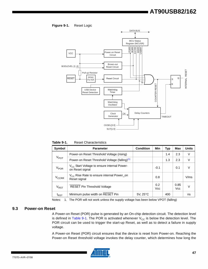
AT90USB82/162
Figure 9-1. Reset Logic
Notes: 1. The POR will not work unless the supply voltage has been below VPOT (falling)
9.3 Power-on ResetA Power-on Reset (POR) pulse is generated by an On-chip detection circuit. The detection level is defined in Table 9-1. The POR is activated whenever VCC is below the detection level. The POR circuit can be used to trigger the start-up Reset, as well as to detect a failure in supply voltage.
A Power-on Reset (POR) circuit ensures that the device is reset from Power-on. Reaching the Power-on Reset threshold voltage invokes the delay counter, which determines how long the
Table 9-1. Reset Characteristics
Symbol Parameter Condition Min Typ Max Units
VPOT
Power-on Reset Threshold Voltage (rising) 1.4 2.3 V
Power-on Reset Threshold Voltage (falling)(1) 1.3 2.3 V
VPORVCC Start Voltage to ensure internal Power-on Reset signal
-0.1 0.1 V
VCCRRVCC Rise Rate to ensure internal Power_on Reset signal
0.8 V/ms
VRST RESET Pin Threshold Voltage0.2 Vcc
0.85 Vcc
V
tRST Minimum pulse width on RESET Pin 5V, 25°C 400 ns
MCU StatusRegister (MCUSR)
Brown-outReset CircuitBODLEVEL [2..0]
Delay Counters
CKSEL[3:0]
CKTIMEOUT
WD
RF
BO
RF
EX
TR
F
PO
RF
DATA BUS
ClockGenerator
SPIKEFILTER
Pull-up Resistor
US
BR
F
USB DeviceReset Detection
WatchdogOscillator
SUT[1:0]
Power-on ResetCircuit
477707D–AVR–07/08

device is kept in RESET after VCC rise. The RESET signal is activated again, without any delay, when VCC decreases below the detection level.
Figure 9-2. MCU Start-up, RESET Tied to VCC
Figure 9-3. MCU Start-up, RESET Extended Externally
9.4 External ResetAn External Reset is generated by a low level on the RESET pin. Reset pulses longer than the minimum pulse width (see Table 9-1) will generate a reset, even if the clock is not running. Shorter pulses are not guaranteed to generate a reset. When the applied signal reaches the Reset Threshold Voltage – VRST – on its positive edge, the delay counter starts the MCU after the Time-out period – tTOUT – has expired.
Figure 9-4. External Reset During Operation
V
RESET
TIME-OUT
INTERNALRESET
tTOUT
VPOT
VRST
CC
RESET
TIME-OUT
INTERNALRESET
tTOUT
VPOT
VRST
VCC
CC
487707D–AVR–07/08
AT90USB82/162

AT90USB82/162
9.5 Brown-out DetectionAT90USB82/162 has an On-chip Brown-out Detection (BOD) circuit for monitoring the VCC level during operation by comparing it to a fixed trigger level. The trigger level for the BOD can be selected by the BODLEVEL Fuses. The trigger level has a hysteresis to ensure spike free Brown-out Detection. The hysteresis on the detection level should be interpreted as VBOT+ = VBOT + VHYST/2 and VBOT- = VBOT - VHYST/2.
Note: 1. VBOT may be below nominal minimum operating voltage for some devices. For devices where this is the case, the device is tested down to VCC = VBOT during the production test. This guar-antees that a Brown-Out Reset will occur before VCC drops to a voltage where correct operation of the microcontroller is no longer guaranteed. The test is performed using BODLEVEL = 110 for AT90USB82/162 and BODLEVEL = 101 for AT90USB82/162L.
When the BOD is enabled, and VCC decreases to a value below the trigger level (VBOT- in Figure 9-5), the Brown-out Reset is immediately activated. When VCC increases above the trigger level (VBOT+ in Figure 9-5), the delay counter starts the MCU after the Time-out period tTOUT has expired.
The BOD circuit will only detect a drop in VCC if the voltage stays below the trigger level for longer than tBOD given in Table 9-1.
Table 9-2. BODLEVEL Fuse Coding(1)
BODLEVEL 2..0 Fuses Min VBOT Typ VBOT Max VBOT Units
111 BOD Disabled
110 2.5 2.7 2.9
V
101 2.7 2.9 3.1
100 2.8 3.0 3.2
011 3.3 3.5 3.7
010 3.4 3.6 3.8
001 3.8 4.0 4.2
000 4.1 4.3 4.5
Table 9-3. Brown-out Characteristics
Symbol Parameter Min Typ Max Units
VHYST Brown-out Detector Hysteresis 50 mV
tBOD Min Pulse Width on Brown-out Reset 2 ns
497707D–AVR–07/08

Figure 9-5. Brown-out Reset During Operation
9.6 Watchdog ResetWhen the Watchdog times out, it will generate a short reset pulse of one CK cycle duration. On the falling edge of this pulse, the delay timer starts counting the Time-out period tTOUT. Refer to page 52 for details on operation of the Watchdog Timer.
Figure 9-6. Watchdog Reset During Operation
9.7 USB ResetWhen the USB macro is enabled and configured with the USB reset MCU feature enabled, and if a valid USB Reset signalling is detected, the microcontroller is reset unless the USB macro that remains enabled. This allows the device to stay attached to the bus during and after the reset, while enhancing firmware reliability.
VCC
RESET
TIME-OUT
INTERNALRESET
VBOT-VBOT+
tTOUT
CK
CC
507707D–AVR–07/08
AT90USB82/162

AT90USB82/162
Figure 9-7. USB Reset During Operation
9.7.1 MCU Status Register –MCUSRThe MCU Status Register provides information on which reset source caused an MCU reset.
• Bit 7-6 – Res: Reserved BitThese bits are reserved and will always read as zero.
• Bit 5 – USBRF: USB Reset FlagThis bit is set if a USB Reset occurs. The bit is reset by a Power-on Reset, or by writing a logic zero to the flag.
• Bit 4– Res: Reserved BitThis bit is reserved.
• Bit 3 – WDRF: Watchdog Reset FlagThis bit is set if a Watchdog Reset occurs. The bit is reset by a Power-on Reset, or by writing a logic zero to the flag.
• Bit 2 – BORF: Brown-out Reset FlagThis bit is set if a Brown-out Reset occurs. The bit is reset by a Power-on Reset, or by writing a logic zero to the flag.
• Bit 1 – EXTRF: External Reset FlagThis bit is set if an External Reset occurs. The bit is reset by a Power-on Reset, or by writing a logic zero to the flag.
• Bit 0 – PORF: Power-on Reset FlagThis bit is set if a Power-on Reset occurs. The bit is reset only by writing a logic zero to the flag.
To make use of the Reset Flags to identify a reset condition, the user should read and then Reset the MCUSR as early as possible in the program. If the register is cleared before another reset occurs, the source of the reset can be found by examining the Reset Flags.
CC
USB Traffic USB TrafficDP
DM
(US
B L
ines
) tUSBRSTMINEnd of Reset
Bit 7 6 5 4 3 2 1 0
– – USBRF – WDRF BORF EXTRF PORF MCUSR
Read/Write R R R R/W R/W R/W R/W R/W
Initial Value 0 0 0 See Bit Description
517707D–AVR–07/08

9.8 Internal Voltage ReferenceAT90USB82/162 features an internal bandgap reference. This reference is used for Brown-out Detection, and it can be used as an input to the Analog Comparator.
9.8.1 Voltage Reference Enable Signals and Start-up TimeThe voltage reference has a start-up time that may influence the way it should be used. The start-up time is given in Table 9-4. To save power, the reference is not always turned on. The reference is on during the following situations:
1. When the BOD is enabled (by programming the BODLEVEL [2..0] Fuse).
2. When the bandgap reference is connected to the Analog Comparator (by setting the ACBG bit in ACSR).
Thus, when the BOD is not enabled, after setting the ACBG bit, the user must always allow the reference to start up before the output from the Analog Comparator is used. To reduce power consumption in Power-down mode, the user can avoid the three conditions above to ensure that the reference is turned off before entering Power-down mode
.
9.9 Watchdog TimerAT90USB82/162 has an Enhanced Watchdog Timer (WDT). The main features are:
• Clocked from separate On-chip Oscillator• 3 Operating modes
– Interrupt– System Reset– Interrupt and System Reset
Table 9-4. Internal Voltage Reference Characteristics
Symbol Parameter Condition Min Typ Max Units
VBG Bandgap reference voltage VCC = 2.7V - 5.5V 1.0 1.1 1.2 V
tBG Bandgap reference start-up time - 40 70 µs
IBGBandgap reference current consumption
- 10 µA
527707D–AVR–07/08
AT90USB82/162

AT90USB82/162
• Selectable Time-out period from 16ms to 8s• Possible Hardware fuse Watchdog always on (WDTON) for fail-safe mode• Early warning after one Time-Out period reached, programmable Reset (see operating modes)
after 2 Time-Out periods reached.
Figure 9-8. Watchdog Timer
The Watchdog Timer (WDT) is a timer counting cycles of a separate on-chip 128 kHz oscillator. The WDT gives a early warning interrupt when the counter reaches a given time-out value. The WDT gives an interrupt or a system reset when the counter reaches two times the given time-out value. In normal operation mode, it is required that the system uses the WDR - Watchdog Timer Reset - instruction to restart the counter before the time-out value is reached. If the system doesn't restart the counter, an interrupt or system reset will be issued.
In Interrupt mode, the WDT gives an interrupt when the timer expires two times. This interrupt can be used to wake the device from sleep-modes, and also as a general system timer. One example is to limit the maximum time allowed for certain operations, giving an interrupt when the operation has run longer than expected.
In System Reset mode, the WDT gives a reset when the timer expires two times. This is typically used to prevent system hang-up in case of runaway code.
The third mode, Interrupt and System Reset mode, combines the other two modes by first giving an interrupt and then switch to System Reset mode. This mode will for instance allow a safe shutdown by saving critical parameters before a system reset.
In addition to these modes, the early warning interrupt can be enabled in order to generate an interrupt when the WDT counter expires the first time.
The Watchdog always on (WDTON) fuse, if programmed, will force the Watchdog Timer to Sys-tem Reset mode. With the fuse programmed the System Reset mode bit (WDE) and Interrupt mode bit (WDIE) are locked to 1 and 0 respectively. To further ensure program security, alter-ations to the Watchdog set-up must follow timed sequences. The sequence for clearing WDE or changing time-out configuration is as follows:
128kHzOSCILLATOR
OSC/
2KOS
C/4K
OSC/
8KOS
C/16
KOS
C/32
KOS
C/64
KOS
C/12
8KOS
C/25
6KOS
C/51
2KOS
C/10
24K
WDP0WDP1WDP2WDP3
WATCHDOGRESET
WDE
WDIF
WDIE
WDEWIE
MCU RESET
INTERRUPT
EARLY WARNINGINTERRUPT
CLOCKDIVIDER
WC
LKD
0W
CLK
D1
OSC/1OSC/3
OSC/5
OSC/7
537707D–AVR–07/08

1. In the same operation, write a logic one to the Watchdog change enable bits WDCE and WDE. A logic one must be written to WDE regardless of the previous value of the WDE bit and even if it will be cleared after the operation.
2. Within the next four clock cycles, write the WDE and Watchdog prescaler bits (WDP) as desired, but with the WDCE bit cleared. This must be done in one operation.
While the WDT prescaler allows only even division factors (2, 4, 8...), the WDT peripheral also includes a clock divider that directly acts on the clock source. This divider handles odd division factors (3, 5, 7). In combination with the prescaler, a large number of time-out values can be obtained.
The divider factor change is also ruled by the secure timed sequence : first the WDE and WDCE bits must be set, and then four cycles are available to load the new divider value into the WDTCKD register. Be aware that after this operation WDE will still be set. So keep in mind the importance of order of operations. When setting up the WDT in Interrupt mode with specific val-ues of prescaler and divider, the divider register must be loaded before the prescaler register :
1. Set WDCE and WDE
2. Load the divider factor into WDTCKD
3. Wait WDCE being automatically cleared (just wait 2 more cycles)
4. Set again WDCE and WDE
5. Clear WDE, set WDIE and load the prescaler factor into WDTCSR in a same operation
6. Now the system is properly configured for Interrupt only mode. Inverting the two opera-tions would have been resulted into “Reset and Interrupt mode” and needed a third operation to clear WDE.
547707D–AVR–07/08
AT90USB82/162

AT90USB82/162
The following code example shows one assembly and one C function for turning off the Watch-dog Timer. The example assumes that interrupts are controlled (e.g. by disabling interrupts globally) so that no interrupts will occur during the execution of these functions.
Note: 1. The example code assumes that the part specific header file is included.
Note: If the Watchdog is accidentally enabled, for example by a runaway pointer or brown-out condition, the device will be reset and the Watchdog Timer will stay enabled. If the code is not set up to handle the Watchdog, this might lead to an eternal loop of time-out resets. To avoid this situation, the application software should always clear the Watchdog System Reset Flag (WDRF) and the WDE control bit in the initialisation routine, even if the Watchdog is not in use.
Assembly Code Example(1)
WDT_off:
; Turn off global interrupt
cli
; Reset Watchdog Timer
wdr
; Clear WDRF in MCUSR
in r16, MCUSR
andi r16, (0xff & (0<<WDRF))
out MCUSR, r16
; Write logical one to WDCE and WDE
; Keep old prescaler setting to prevent unintentional time-out
in r16, WDTCSR
ori r16, (1<<WDCE) | (1<<WDE)
out WDTCSR, r16
; Turn off WDT
ldi r16, (0<<WDE)
out WDTCSR, r16
; Turn on global interrupt
sei
ret
C Code Example(1)
void WDT_off(void)
{
__disable_interrupt();
__watchdog_reset();
/* Clear WDRF in MCUSR */
MCUSR &= ~(1<<WDRF);
/* Write logical one to WDCE and WDE */
/* Keep old prescaler setting to prevent unintentional time-out */
WDTCSR |= (1<<WDCE) | (1<<WDE);
/* Turn off WDT */
WDTCSR = 0x00;
__enable_interrupt();
}
557707D–AVR–07/08

The following code example shows one assembly and one C function for changing the time-out value of the Watchdog Timer.
Note: 1. The example code assumes that the part specific header file is included.
Note: The Watchdog Timer should be reset before any change of the WDP bits, since a change in the WDP bits can result in a time-out when switching to a shorter time-out period.
9.9.1 Watchdog Timer Control Register - WDTCSR
• Bit 7 - WDIF: Watchdog Interrupt FlagThis bit is set when a time-out occurs twice in the Watchdog Timer and if the Watchdog Timer is configured for interrupt. WDIF is automatically cleared by hardware when executing the corre-
Assembly Code Example(1)
WDT_Prescaler_Change:
; Turn off global interrupt
cli
; Reset Watchdog Timer
wdr
; Start timed sequence
in r16, WDTCSR
ori r16, (1<<WDCE) | (1<<WDE)
out WDTCSR, r16
; -- Got four cycles to set the new values from here -
; Set new prescaler(time-out) value = 64K cycles (~0.5 s)
ldi r16, (1<<WDE) | (1<<WDP2) | (1<<WDP0)
out WDTCSR, r16
; -- Finished setting new values, used 2 cycles -
; Turn on global interrupt
sei
ret
C Code Example(1)
void WDT_Prescaler_Change(void)
{
__disable_interrupt();
__watchdog_reset();
/* Start timed equence */
WDTCSR |= (1<<WDCE) | (1<<WDE);
/* Set new prescaler(time-out) value = 64K cycles (~0.5 s) */
WDTCSR = (1<<WDE) | (1<<WDP2) | (1<<WDP0);
__enable_interrupt();
}
Bit 7 6 5 4 3 2 1 0
WDIF WDIE WDP3 WDCE WDE WDP2 WDP1 WDP0 WDTCSR
Read/Write R/W R/W R/W R/W R/W R/W R/W R/W
Initial Value 0 0 0 0 X 0 0 0
567707D–AVR–07/08
AT90USB82/162

AT90USB82/162
sponding interrupt handling vector. Alternatively, WDIF is cleared by writing a logic one to the flag. When the I-bit in SREG and WDIE are set, the Watchdog Time-out Interrupt is executed.
• Bit 6 - WDIE: Watchdog Interrupt EnableWhen this bit is written to one and the I-bit in the Status Register is set, the Watchdog Interrupt is enabled. If WDE is cleared in combination with this setting, the Watchdog Timer is in Interrupt Mode, and the corresponding interrupt is executed if time-out in the Watchdog Timer occurs.
If WDE is set, the Watchdog Timer is in Interrupt and System Reset Mode. Two consecutives times-out in the Watchdog Timer will set WDIF. Executing the corresponding interrupt vector will clear WDIE and WDIF automatically by hardware : the Watchdog goes to System Reset Mode. This is useful for keeping the Watchdog Timer security while using the interrupt. To reinitialize the Interrupt and System Reset Mode, WDIE must be set after each interrupt. This should how-ever not be done within the interrupt service routine itself, as this might compromise the safety-function of the Watchdog System Reset mode. If the interrupt is not executed before the next time-out, a System Reset will be applied.
• Bit 4 - WDCE: Watchdog Change EnableThis bit is used in timed sequences for changing WDE and prescaler bits. To clear the WDE bit, and/or change the prescaler bits, WDCE must be set.
Once written to one, hardware will clear WDCE after four clock cycles.
• Bit 3 - WDE: Watchdog System Reset EnableWDE is overridden by WDRF in MCUSR. This means that WDE is always set when WDRF is set. To clear WDE, WDRF must be cleared first. This feature ensures multiple resets during con-ditions causing failure, and a safe start-up after the failure.
• Bit 5, 2..0 - WDP3..0: Watchdog Timer Prescaler 3, 2, 1 and 0The WDP3..0 bits determine the Watchdog Timer prescaling when the Watchdog Timer is run-ning. The different prescaling values and their corresponding time-out periods are shown in Table 9-6 on page 59.
9.9.2 Watchdog Timer Clock Divider Register - WDTCKD
Table 9-5. Watchdog Timer Configuration
WDTON (Fuse) WDE WDIE Mode Action on 2x Time-out
1 (unprogrammed) 0 0 Stopped None
1 (unprogrammed) 0 1 Interrupt Mode Interrupt
1 (unprogrammed) 1 0 System Reset Mode Reset
1 (unprogrammed) 1 1Interrupt and System Reset Mode
Interrupt, then go to System Reset Mode
0 (programmed) x x System Reset Mode Reset
Bit 7 6 5 4 3 2 1 0
- - - - WDE-WIF
WDEW-IE
WCLKD1
WCLKD0
WDTCKD
Read/Write R/W R/W R/W R/W R/W R/W R/W R/W
Initial Value 0 0 0 0 0 0 0 0
577707D–AVR–07/08

• Bit 7-4 - Reserved bitsThese bits are reserved and will always read as zero.
• Bit 3 - WDEWIF: Watchdog Early Warning Interrupt FlagThis bit is set when a first time-out occurs in the Watchdog Timer and if the WDEWIE bit is enabled. WDEWIF is automatically cleared by hardware when executing the corresponding interrupt handling vector. Alternatively, WDIF can be cleared by writing a logic one to the flag. When the I-bit in SREG and WDEWIE are set, the Watchdog Time-out Interrupt is executed.
• Bit 2 - WDEWIE: Watchdog Early Warning Interrupt EnableWhen this bit has been set by software, an interrupt will be generated on the watchdog interrupt vector when the Early warning flag is set to one by hardware.
• Bit 1:0 - WCLKD[1:0]: Watchdog Timer Clock Divider
– WCLKD = 0 : ClkWDT = Clk128k
– WCLKD = 1 : ClkWDT = Clk128k / 3
– WCLKD = 2 : ClkWDT = Clk128k / 5
– WCLKD = 3 : ClkWDT = Clk128k / 7
587707D–AVR–07/08
AT90USB82/162

AT90USB82/162
.
Table 9-6. Watchdog Timer Prescale Select, DIV = 0 (CLKwdt = CLK128 / 1)
WDP3 WDP2 WDP1 WDP0
Number of WDT Oscillator Cycles before 1st time-out
(Early warning)
Early warning Typical Time-out at VCC = 5.0V
Watchdog Reset/Interrupt Typical
Time-out at VCC = 5.0V
0 0 0 0 2K (2048) cycles 16 ms 32 ms
0 0 0 1 4K (4096) cycles 32 ms 64 ms
0 0 1 0 8K (8192) cycles 64 ms 128 ms
0 0 1 1 16K (16384) cycles 0.125 s 0.250 s
0 1 0 0 32K (32768) cycles 0.25 s 0.5 s
0 1 0 1 64K (65536) cycles 0.5 s 1.0 s
0 1 1 0 128K (131072) cycles 1.0 s 2.0 s
0 1 1 1 256K (262144) cycles 2.0 s 4.0 s
1 0 0 0 512K (524288) cycles 4.0 s 8.0 s
1 0 0 1 1024K (1048576) cycles 8.0 s 16.0 s
1 0 1 0
Reserved
1 0 1 1
1 1 0 0
1 1 0 1
1 1 1 0
1 1 1 1
597707D–AVR–07/08

Table 9-7. Watchdog Timer Prescale Select, DIV = 1 (CLKwdt = CLK128 / 3)
WDP3 WDP2 WDP1 WDP0
Number of WDT Oscillator Cycles before 1st time-out
(Early warning)
Early warning Typical Time-out at VCC = 5.0V
Watchdog Reset/Interrupt Typical
Time-out at VCC = 5.0V
0 0 0 0 2K (2048) cycles 48 ms 96 ms
0 0 0 1 4K (4096) cycles 96 ms 192 ms
0 0 1 0 8K (8192) cycles 192 ms 384 ms
0 0 1 1 16K (16384) cycles 0.375 s 0.75 s
0 1 0 0 32K (32768) cycles 0.75 s 1.5 s
0 1 0 1 64K (65536) cycles 1.5 s 3 s
0 1 1 0 128K (131072) cycles 3 s 6 s
0 1 1 1 256K (262144) cycles 6 s 12 s
1 0 0 0 512K (524288) cycles 12 s 24 s
1 0 0 1 1024K (1048576) cycles 24 s 48 s
1 0 1 0
Reserved
1 0 1 1
1 1 0 0
1 1 0 1
1 1 1 0
1 1 1 1
607707D–AVR–07/08
AT90USB82/162

AT90USB82/162
Table 9-8. Watchdog Timer Prescale Select, DIV = 2 (CLKwdt = CLK128 / 5)
WDP3 WDP2 WDP1 WDP0
Number of WDT Oscillator Cycles before 1st time-out
(Early warning)
Early warning Typical Time-out at VCC = 5.0V
Watchdog Reset/Interrupt Typical
Time-out at VCC = 5.0V
0 0 0 0 2K (2048) cycles 80 ms 160 ms
0 0 0 1 4K (4096) cycles 160 ms 320 ms
0 0 1 0 8K (8192) cycles 320 ms 640 ms
0 0 1 1 16K (16384) cycles 0.625 s 1.25 s
0 1 0 0 32K (32768) cycles 1.25 s 2.5 s
0 1 0 1 64K (65536) cycles 2.5 s 5 s
0 1 1 0 128K (131072) cycles 5 s 10 s
0 1 1 1 256K (262144) cycles 10 s 20 s
1 0 0 0 512K (524288) cycles 20 s 40 s
1 0 0 1 1024K (1048576) cycles 40 s 80 s
1 0 1 0
Reserved
1 0 1 1
1 1 0 0
1 1 0 1
1 1 1 0
1 1 1 1
617707D–AVR–07/08

Table 9-9. Watchdog Timer Prescale Select, DIV = 3 (CLKwdt = CLK128 / 7)
WDP3 WDP2 WDP1 WDP0
Number of WDT Oscillator Cycles before 1st time-out
(Early warning)
Early warning Typical Time-out at VCC = 5.0V
Watchdog Reset/Interrupt Typical
Time-out at VCC = 5.0V
0 0 0 0 2K (2048) cycles 112 ms 224 ms
0 0 0 1 4K (4096) cycles 224 ms 448 ms
0 0 1 0 8K (8192) cycles 448 ms 896 ms
0 0 1 1 16K (16384) cycles 0.875 s 1.75 s
0 1 0 0 32K (32768) cycles 1.75 s 3.5 s
0 1 0 1 64K (65536) cycles 3.5 s 7 s
0 1 1 0 128K (131072) cycles 7 s 14 s
0 1 1 1 256K (262144) cycles 14 s 28 s
1 0 0 0 512K (524288) cycles 28 s 56 s
1 0 0 1 1024K (1048576) cycles 56 s 112 s
1 0 1 0
Reserved
1 0 1 1
1 1 0 0
1 1 0 1
1 1 1 0
1 1 1 1
627707D–AVR–07/08
AT90USB82/162

AT90USB82/162
10. InterruptsThis section describes the specifics of the interrupt handling as performed in AT90USB82/162. For a general explanation of the AVR interrupt handling, refer to “Reset and Interrupt Handling” on page 13.
10.1 Interrupt Vectors in AT90USB82/162
Table 10-1. Reset and Interrupt Vectors
VectorNo.
ProgramAddress(2) Source Interrupt Definition
1 $0000(1) RESETExternal Pin, Power-on Reset, Brown-out Reset, Watchdog Reset, USB Reset and debugWIRE AVR Reset
2 $0002 INT0 External Interrupt Request 0
3 $0004 INT1 External Interrupt Request 1
4 $0006 INT2 External Interrupt Request 2
5 $0008 INT3 External Interrupt Request 3
6 $000A INT4 External Interrupt Request 4
7 $000C INT5 External Interrupt Request 5
8 $000E INT6 External Interrupt Request 6
9 $0010 INT7 External Interrupt Request 7
10 $0012 PCINT0 Pin Change Interrupt Request 0
11 $0014 PCINT1 Pin Change Interrupt Request 1
12 $0016 USB General USB General Interrupt request
13 $0018 USB Endpoint USB Endpoint Interrupt request
14 $001A WDT Watchdog Time-out Interrupt
15 $001C TIMER1 CAPT Timer/Counter1 Capture Event
16 $001E TIMER1 COMPA Timer/Counter1 Compare Match A
17 $0020 TIMER1 COMPB Timer/Counter1 Compare Match B
18 $0022 TIMER1 COMPC Timer/Counter1 Compare Match C
19 $0024 TIMER1 OVF Timer/Counter1 Overflow
20 $0026 TIMER0 COMPA Timer/Counter0 Compare Match A
21 $0028 TIMER0 COMPB Timer/Counter0 Compare match B
22 $002A TIMER0 OVF Timer/Counter0 Overflow
23 $002C SPI, STC SPI Serial Transfer Complete
24 $002E USART1 RX USART1 Rx Complete
25 $0030 USART1 UDRE USART1 Data Register Empty
26 $0032 USART1TX USART1 Tx Complete
637707D–AVR–07/08

Notes: 1. When the BOOTRST Fuse is programmed, the device will jump to the Boot Loader address at reset, see “Memory Programming” on page 243.
2. When the IVSEL bit in MCUCR is set, Interrupt Vectors will be moved to the start of the Boot Flash Section. The address of each Interrupt Vector will then be the address in this table added to the start address of the Boot Flash Section. Moreover, contrary to other 8K/16K devices, the interrupt vectors spacing remains identical (2 words) for both 8KB and 16KB versions.
Table 10-2 shows reset and Interrupt Vectors placement for the various combinations of BOOTRST and IVSEL settings. If the program never enables an interrupt source, the Interrupt Vectors are not used, and regular program code can be placed at these locations. This is also the case if the Reset Vector is in the Application section while the Interrupt Vectors are in the Boot section or vice versa.
27 $0034 ANALOG COMP Analog Comparator
28 $0036 EE READY EEPROM Ready
29 $0038 SPM READY Store Program Memory Ready
Table 10-1. Reset and Interrupt Vectors (Continued)
VectorNo.
ProgramAddress(2) Source Interrupt Definition
647707D–AVR–07/08
AT90USB82/162

AT90USB82/162
Note: 1. The Boot Reset Address is shown in Table 23-8 on page 239. For the BOOTRST Fuse “1” means unprogrammed while “0” means programmed.
10.1.1 Moving Interrupts Between Application and Boot SpaceThe General Interrupt Control Register controls the placement of the Interrupt Vector table.
10.1.2 MCU Control Register – MCUCR
• Bit 1 – IVSEL: Interrupt Vector SelectWhen the IVSEL bit is cleared (zero), the Interrupt Vectors are placed at the start of the Flash memory. When this bit is set (one), the Interrupt Vectors are moved to the beginning of the Boot Loader section of the Flash. The actual address of the start of the Boot Flash Section is deter-mined by the BOOTSZ Fuses. Refer to the section “Memory Programming” on page 243 for details. To avoid unintentional changes of Interrupt Vector tables, a special write procedure must be followed to change the IVSEL bit:
a. Write the Interrupt Vector Change Enable (IVCE) bit to one.
b. Within four cycles, write the desired value to IVSEL while writing a zero to IVCE.
Interrupts will automatically be disabled while this sequence is executed. Interrupts are disabled in the cycle IVCE is set, and they remain disabled until after the instruction following the write to IVSEL. If IVSEL is not written, interrupts remain disabled for four cycles. The I-bit in the Status Register is unaffected by the automatic disabling.
Note: If Interrupt Vectors are placed in the Boot Loader section and Boot Lock bit BLB02 is pro-grammed, interrupts are disabled while executing from the Application section. If Interrupt Vectors are placed in the Application section and Boot Lock bit BLB12 is programed, interrupts are dis-abled while executing from the Boot Loader section. Refer to the section “Memory Programming” on page 243 for details on Boot Lock bits.
• Bit 0 – IVCE: Interrupt Vector Change Enable
Table 10-2. Reset and Interrupt Vectors Placement(1)
BOOTRST IVSEL Reset Address Interrupt Vectors Start Address
1 0 0x0000 0x0002
1 1 0x0000 Boot Reset Address + 0x0002
0 0 Boot Reset Address 0x0002
0 1 Boot Reset Address Boot Reset Address + 0x0002
Bit 7 6 5 4 3 2 1 0
JTD – – PUD – – IVSEL IVCE MCUCR
Read/Write R/W R R R/W R R R/W R/W
Initial Value 0 0 0 0 0 0 0 0
657707D–AVR–07/08

The IVCE bit must be written to logic one to enable change of the IVSEL bit. IVCE is cleared by hardware four cycles after it is written or when IVSEL is written. Setting the IVCE bit will disable interrupts, as explained in the IVSEL description above. See Code Example below.
Assembly Code Example
Move_interrupts:
; Enable change of Interrupt Vectors
ldi r16, (1<<IVCE)
out MCUCR, r16
; Move interrupts to Boot Flash section
ldi r16, (1<<IVSEL)
out MCUCR, r16
ret
C Code Example
void Move_interrupts(void)
{
/* Enable change of Interrupt Vectors */
MCUCR = (1<<IVCE);
/* Move interrupts to Boot Flash section */
MCUCR = (1<<IVSEL);
}
667707D–AVR–07/08
AT90USB82/162

AT90USB82/162
11. I/O-Ports
11.1 IntroductionAll AVR ports have true Read-Modify-Write functionality when used as general digital I/O ports. This means that the direction of one port pin can be changed without unintentionally changing the direction of any other pin with the SBI and CBI instructions. The same applies when chang-ing drive value (if configured as output) or enabling/disabling of pull-up resistors (if configured as input). Each output buffer has symmetrical drive characteristics with both high sink and source capability. The pin driver is strong enough to drive LED displays directly. All port pins have indi-vidually selectable pull-up resistors with a supply-voltage invariant resistance. All I/O pins have protection diodes to both VCC and Ground as indicated in Figure 11-1. Refer to “Electrical Char-acteristics” on page 262 for a complete list of parameters.
Figure 11-1. I/O Pin Equivalent Schematic
All registers and bit references in this section are written in general form. A lower case “x” repre-sents the numbering letter for the port, and a lower case “n” represents the bit number. However, when using the register or bit defines in a program, the precise form must be used. For example, PORTB3 for bit no. 3 in Port B, here documented generally as PORTxn. The physical I/O Regis-ters and bit locations are listed in “Register Description for I/O-Ports” on page 82.
Three I/O memory address locations are allocated for each port, one each for the Data Register – PORTx, Data Direction Register – DDRx, and the Port Input Pins – PINx. The Port Input Pins I/O location is read only, while the Data Register and the Data Direction Register are read/write. However, writing a logic one to a bit in the PINx Register, will result in a toggle in the correspond-ing bit in the Data Register. In addition, the Pull-up Disable – PUD bit in MCUCR disables the pull-up function for all pins in all ports when set.
Using the I/O port as General Digital I/O is described in “Ports as General Digital I/O” on page 68. Most port pins are multiplexed with alternate functions for the peripheral features on the device. How each alternate function interferes with the port pin is described in “Alternate Port Functions” on page 72. Refer to the individual module sections for a full description of the alter-nate functions.
Cpin
Logic
Rpu
See Figure"General Digital I/O" for
Details
Pxn
677707D–AVR–07/08

Note that enabling the alternate function of some of the port pins does not affect the use of the other pins in the port as general digital I/O.
11.2 Ports as General Digital I/OThe ports are bi-directional I/O ports with optional internal pull-ups. Figure 11-2 shows a func-tional description of one I/O-port pin, here generically called Pxn.
Figure 11-2. General Digital I/O(1)
Note: 1. WRx, WPx, WDx, RRx, RPx, and RDx are common to all pins within the same port. clkI/O, SLEEP, and PUD are common to all ports.
11.2.1 Configuring the PinEach port pin consists of three register bits: DDxn, PORTxn, and PINxn. As shown in “Register Description for I/O-Ports” on page 82, the DDxn bits are accessed at the DDRx I/O address, the PORTxn bits at the PORTx I/O address, and the PINxn bits at the PINx I/O address.
The DDxn bit in the DDRx Register selects the direction of this pin. If DDxn is written logic one, Pxn is configured as an output pin. If DDxn is written logic zero, Pxn is configured as an input pin.
If PORTxn is written logic one when the pin is configured as an input pin, the pull-up resistor is activated. To switch the pull-up resistor off, PORTxn has to be written logic zero or the pin has to be configured as an output pin. The port pins are tri-stated when reset condition becomes active, even if no clocks are running.
clk
RPx
RRx
RDx
WDx
PUD
SYNCHRONIZER
WDx: WRITE DDRx
WRx: WRITE PORTxRRx: READ PORTx REGISTERRPx: READ PORTx PIN
PUD: PULLUP DISABLE
clkI/O: I/O CLOCK
RDx: READ DDRx
D
L
Q
Q
RESET
RESET
Q
QD
Q
Q D
CLR
PORTxn
Q
Q D
CLR
DDxn
PINxn
DAT
A B
US
SLEEP
SLEEP: SLEEP CONTROL
Pxn
I/O
WPx
0
1
WRx
WPx: WRITE PINx REGISTER
687707D–AVR–07/08
AT90USB82/162
AT90USB82/162
If PORTxn is written logic one when the pin is configured as an output pin, the port pin is driven high (one). If PORTxn is written logic zero when the pin is configured as an output pin, the port pin is driven low (zero).
11.2.2 Toggling the PinWriting a logic one to PINxn toggles the value of PORTxn, independent on the value of DDRxn. Note that the SBI instruction can be used to toggle one single bit in a port.
11.2.3 Switching Between Input and OutputWhen switching between tri-state ({DDxn, PORTxn} = 0b00) and output high ({DDxn, PORTxn} = 0b11), an intermediate state with either pull-up enabled {DDxn, PORTxn} = 0b01) or output low ({DDxn, PORTxn} = 0b10) occurs. Normally, the pull-up enabled state is fully acceptable, as a high-impedant environment will not notice the difference between a strong high driver and a pull-up. If this is not the case, the PUD bit in the MCUCR Register can be set to disable all pull-ups in all ports.
Switching between input with pull-up and output low generates the same problem. The user must use either the tri-state ({DDxn, PORTxn} = 0b00) or the output high state ({DDxn, PORTxn} = 0b11) as an intermediate step.
Table 11-1 summarizes the control signals for the pin value.
11.2.4 Reading the Pin ValueIndependent of the setting of Data Direction bit DDxn, the port pin can be read through the PINxn Register bit. As shown in Figure 11-2, the PINxn Register bit and the preceding latch con-stitute a synchronizer. This is needed to avoid metastability if the physical pin changes value near the edge of the internal clock, but it also introduces a delay. Figure 11-3 shows a timing dia-gram of the synchronization when reading an externally applied pin value. The maximum and minimum propagation delays are denoted tpd,max and tpd,min respectively.
Table 11-1. Port Pin Configurations
DDxn PORTxnPUD
(in MCUCR) I/O Pull-up Comment
0 0 X Input No Tri-state (Hi-Z)
0 1 0 Input YesPxn will source current if ext. pulled low.
0 1 1 Input No Tri-state (Hi-Z)
1 0 X Output No Output Low (Sink)
1 1 X Output No Output High (Source)
697707D–AVR–07/08

Figure 11-3. Synchronization when Reading an Externally Applied Pin value
Consider the clock period starting shortly after the first falling edge of the system clock. The latch is closed when the clock is low, and goes transparent when the clock is high, as indicated by the shaded region of the “SYNC LATCH” signal. The signal value is latched when the system clock goes low. It is clocked into the PINxn Register at the succeeding positive clock edge. As indi-cated by the two arrows tpd,max and tpd,min, a single signal transition on the pin will be delayed between ½ and 1½ system clock period depending upon the time of assertion.
When reading back a software assigned pin value, a nop instruction must be inserted as indi-cated in Figure 11-4. The out instruction sets the “SYNC LATCH” signal at the positive edge of the clock. In this case, the delay tpd through the synchronizer is 1 system clock period.
Figure 11-4. Synchronization when Reading a Software Assigned Pin Value
The following code example shows how to set port B pins 0 and 1 high, 2 and 3 low, and define the port pins from 4 to 7 as input with pull-ups assigned to port pins 6 and 7. The resulting pin values are read back again, but as previously discussed, a nop instruction is included to be able to read back the value recently assigned to some of the pins.
XXX in r17, PINx
0x00 0xFF
INSTRUCTIONS
SYNC LATCH
PINxn
r17
XXX
SYSTEM CLK
tpd, max
tpd, min
out PORTx, r16 nop in r17, PINx
0xFF
0x00 0xFF
SYSTEM CLK
r16
INSTRUCTIONS
SYNC LATCH
PINxn
r17tpd
707707D–AVR–07/08
AT90USB82/162

AT90USB82/162
Note: 1. For the assembly program, two temporary registers are used to minimize the time from pull-ups are set on pins 0, 1, 6, and 7, until the direction bits are correctly set, defining bit 2 and 3 as low and redefining bits 0 and 1 as strong high drivers.
11.2.5 Digital Input Enable and Sleep ModesAs shown in Figure 11-2, the digital input signal can be clamped to ground at the input of the schmitt-trigger. The signal denoted SLEEP in the figure, is set by the MCU Sleep Controller in Power-down mode, Power-save mode, and Standby mode to avoid high power consumption if some input signals are left floating, or have an analog signal level close to VCC/2.
SLEEP is overridden for port pins enabled as external interrupt pins. If the external interrupt request is not enabled, SLEEP is active also for these pins. SLEEP is also overridden by various other alternate functions as described in “Alternate Port Functions” on page 72.
If a logic high level (“one”) is present on an asynchronous external interrupt pin configured as “Interrupt on Rising Edge, Falling Edge, or Any Logic Change on Pin” while the external interrupt is not enabled, the corresponding External Interrupt Flag will be set when resuming from the above mentioned Sleep mode, as the clamping in these sleep mode produces the requested logic change.
Assembly Code Example(1)
...
; Define pull-ups and set outputs high
; Define directions for port pins
ldi r16,(1<<PB7)|(1<<PB6)|(1<<PB1)|(1<<PB0)
ldi r17,(1<<DDB3)|(1<<DDB2)|(1<<DDB1)|(1<<DDB0)
out PORTB,r16
out DDRB,r17
; Insert nop for synchronization
nop
; Read port pins
in r16,PINB
...
C Code Example
unsigned char i;
...
/* Define pull-ups and set outputs high */
/* Define directions for port pins */
PORTB = (1<<PB7)|(1<<PB6)|(1<<PB1)|(1<<PB0);
DDRB = (1<<DDB3)|(1<<DDB2)|(1<<DDB1)|(1<<DDB0);
/* Insert nop for synchronization*/
__no_operation();
/* Read port pins */
i = PINB;
...
717707D–AVR–07/08

11.2.6 Unconnected PinsIf some pins are unused, it is recommended to ensure that these pins have a defined level. Even though most of the digital inputs are disabled in the deep sleep modes as described above, float-ing inputs should be avoided to reduce current consumption in all other modes where the digital inputs are enabled (Reset, Active mode and Idle mode).
The simplest method to ensure a defined level of an unused pin, is to enable the internal pull-up. In this case, the pull-up will be disabled during reset. If low power consumption during reset is important, it is recommended to use an external pull-up or pull-down. Connecting unused pins directly to VCC or GND is not recommended, since this may cause excessive currents if the pin is accidentally configured as an output.
11.3 Alternate Port FunctionsMost port pins have alternate functions in addition to being general digital I/Os. Figure 11-5shows how the port pin control signals from the simplified Figure 11-2 can be overridden by alternate functions. The overriding signals may not be present in all port pins, but the figure serves as a generic description applicable to all port pins in the AVR microcontroller family.
Figure 11-5. Alternate Port Functions(1)
clk
RPx
RRxWRx
RDx
WDx
PUD
SYNCHRONIZER
WDx: WRITE DDRx
WRx: WRITE PORTxRRx: READ PORTx REGISTER
RPx: READ PORTx PIN
PUD: PULLUP DISABLE
clkI/O: I/O CLOCK
RDx: READ DDRx
D
L
Q
Q
SET
CLR
0
1
0
1
0
1
DIxn
AIOxn
DIEOExn
PVOVxn
PVOExn
DDOVxn
DDOExn
PUOExn
PUOVxn
PUOExn: Pxn PULL-UP OVERRIDE ENABLEPUOVxn: Pxn PULL-UP OVERRIDE VALUEDDOExn: Pxn DATA DIRECTION OVERRIDE ENABLEDDOVxn: Pxn DATA DIRECTION OVERRIDE VALUEPVOExn: Pxn PORT VALUE OVERRIDE ENABLEPVOVxn: Pxn PORT VALUE OVERRIDE VALUE
DIxn: DIGITAL INPUT PIN n ON PORTxAIOxn: ANALOG INPUT/OUTPUT PIN n ON PORTx
RESET
RESET
Q
Q D
CLR
Q
Q D
CLR
Q
QD
CLR
PINxn
PORTxn
DDxn
DAT
A B
US
0
1DIEOVxn
SLEEP
DIEOExn: Pxn DIGITAL INPUT-ENABLE OVERRIDE ENABLEDIEOVxn: Pxn DIGITAL INPUT-ENABLE OVERRIDE VALUESLEEP: SLEEP CONTROL
Pxn
I/O
0
1
PTOExn
PTOExn: Pxn, PORT TOGGLE OVERRIDE ENABLE
WPx: WRITE PINx
WPx
727707D–AVR–07/08
AT90USB82/162

AT90USB82/162
Note: 1. WRx, WPx, WDx, RRx, RPx, and RDx are common to all pins within the same port. clkI/O, SLEEP, and PUD are common to all ports. All other signals are unique for each pin.
Table 11-2 summarizes the function of the overriding signals. The pin and port indexes from Fig-ure 11-5 are not shown in the succeeding tables. The overriding signals are generated internally in the modules having the alternate function.
The following subsections shortly describe the alternate functions for each port, and relate the overriding signals to the alternate function. Refer to the alternate function description for further details.
11.3.1 MCU Control Register – MCUCR
Table 11-2. Generic Description of Overriding Signals for Alternate Functions
Signal Name Full Name Description
PUOEPull-up Override Enable
If this signal is set, the pull-up enable is controlled by the PUOV signal. If this signal is cleared, the pull-up is enabled when {DDxn, PORTxn, PUD} = 0b010.
PUOVPull-up Override Value
If PUOE is set, the pull-up is enabled/disabled when PUOV is set/cleared, regardless of the setting of the DDxn, PORTxn, and PUD Register bits.
DDOEData Direction Override Enable
If this signal is set, the Output Driver Enable is controlled by the DDOV signal. If this signal is cleared, the Output driver is enabled by the DDxn Register bit.
DDOVData Direction Override Value
If DDOE is set, the Output Driver is enabled/disabled when DDOV is set/cleared, regardless of the setting of the DDxn Register bit.
PVOEPort Value Override Enable
If this signal is set and the Output Driver is enabled, the port value is controlled by the PVOV signal. If PVOE is cleared, and the Output Driver is enabled, the port Value is controlled by the PORTxn Register bit.
PVOVPort Value Override Value
If PVOE is set, the port value is set to PVOV, regardless of the setting of the PORTxn Register bit.
PTOEPort Toggle Override Enable
If PTOE is set, the PORTxn Register bit is inverted.
DIEOEDigital Input Enable Override Enable
If this bit is set, the Digital Input Enable is controlled by the DIEOV signal. If this signal is cleared, the Digital Input Enable is determined by MCU state (Normal mode, sleep mode).
DIEOVDigital Input Enable Override Value
If DIEOE is set, the Digital Input is enabled/disabled when DIEOV is set/cleared, regardless of the MCU state (Normal mode, sleep mode).
DI Digital Input
This is the Digital Input to alternate functions. In the figure, the signal is connected to the output of the schmitt trigger but before the synchronizer. Unless the Digital Input is used as a clock source, the module with the alternate function will use its own synchronizer.
AIOAnalog Input/Output
This is the Analog Input/output to/from alternate functions. The signal is connected directly to the pad, and can be used bi-directionally.
Bit 7 6 5 4 3 2 1 0
JTD – – PUD – – IVSEL IVCE MCUCR
737707D–AVR–07/08

• Bit 4 – PUD: Pull-up DisableWhen this bit is written to one, the pull-ups in the I/O ports are disabled even if the DDxn and PORTxn Registers are configured to enable the pull-ups ({DDxn, PORTxn} = 0b01). See “Con-figuring the Pin” on page 68 for more details about this feature.
11.3.2 Alternate Functions of Port BThe Port B pins with alternate functions are shown in Table 11-3.
The alternate pin configuration is as follows:
• OC0A/OC1C/PCINT7, Bit 7OC0A, Output Compare Match A output: The PB7 pin can serve as an external output for the Timer/Counter0 Output Compare. The pin has to be configured as an output (DDB7 set “one”) to serve this function. The OC0A pin is also the output pin for the PWM mode timer function.
OC1C, Output Compare Match C output: The PB7 pin can serve as an external output for the Timer/Counter1 Output Compare C. The pin has to be configured as an output (DDB7 set “one”) to serve this function. The OC1C pin is also the output pin for the PWM mode timer function.
PCINT7, Pin Change Interrupt source 7: The PB7 pin can serve as an external interrupt source.
• PCINT6, Bit 6PCINT6, Pin Change Interrupt source 6: The PB6 pin can serve as an external interrupt source.
• PCINT5, Bit 5PCINT5, Pin Change Interrupt source 5: The PB5 pin can serve as an external interrupt source.
• T1/PCINT4, Bit 4T1, Timer/Counter1 counter source.
PCINT4, Pin Change Interrupt source 4: The PB4 pin can serve as an external interrupt source.
• PDO/MISO/PCINT3 – Port B, Bit 3
Read/Write R/W R R R/W R R R/W R/W
Initial Value 0 0 0 0 0 0 0 0
Table 11-3. Port B Pins Alternate Functions
Port Pin Alternate Functions
PB7OC0A/OC1C/PCINT7 (Output Compare and PWM Output A for Timer/Counter0, Output Compare and PWM Output C for Timer/Counter1 or Pin Change Interrupt 7)
PB6 PCINT6 (Pin Change Interrupt 6)
PB5 PCINT5 (Pin Change Interrupt 5)
PB4 T1/PCINT4 (Timer/Counter1 Clock Input or Pin Change Interrupt 4)
PB3PDO/MISO/PCINT3 (Programming Data Output or SPI Bus Master Input/Slave Output or Pin Change Interrupt 3)
PB2PDI/MOSI/PCINT2 (Programming Data Input or SPI Bus Master Output/Slave Input or Pin Change Interrupt 2)
PB1 SCLK/PCINT1 (SPI Bus Serial Clock or Pin Change Interrupt 1)
PB0 SS/PCINT0 (SPI Slave Select input or Pin Change Interrupt 0)
747707D–AVR–07/08
AT90USB82/162

AT90USB82/162
PDO, SPI Serial Programming Data Output. During Serial Program Downloading, this pin is used as data output line for the AT90USB82/162.
MISO: Master Data input, Slave Data output pin for SPI channel. When the SPI is enabled as a master, this pin is configured as an input regardless of the setting of DDB3. When the SPI is enabled as a slave, the data direction of this pin is controlled by DDB3. When the pin is forced to be an input, the pull-up can still be controlled by the PORTB3 bit.
PCINT3, Pin Change Interrupt source 3: The PB3 pin can serve as an external interrupt source.
• PDI/MOSI/PCINT2 – Port B, Bit 2PDI, SPI Serial Programming Data Input. During Serial Program Downloading, this pin is used as data input line for the AT90USB82/162.
MOSI: SPI Master Data output, Slave Data input for SPI channel. When the SPI is enabled as a slave, this pin is configured as an input regardless of the setting of DDB2. When the SPI is enabled as a master, the data direction of this pin is controlled by DDB2. When the pin is forced to be an input, the pull-up can still be controlled by the PORTB2 bit.
PCINT2, Pin Change Interrupt source 2: The PB2 pin can serve as an external interrupt source.
• SCK/PCINT1 – Port B, Bit 1SCK: Master Clock output, Slave Clock input pin for SPI channel. When the SPI is enabled as a slave, this pin is configured as an input regardless of the setting of DDB1. When the SPI0 is enabled as a master, the data direction of this pin is controlled by DDB1. When the pin is forced to be an input, the pull-up can still be controlled by the PORTB1 bit. This pin also serves as Clock for the Serial Programming interface.
PCINT1, Pin Change Interrupt source 1: The PB1 pin can serve as an external interrupt source.
• SS/PCINT0 – Port B, Bit 0SS: Slave Port Select input. When the SPI is enabled as a slave, this pin is configured as an input regardless of the setting of DDB0. As a slave, the SPI is activated when this pin is driven low. When the SPI is enabled as a master, the data direction of this pin is controlled by DDB0. When the pin is forced to be an input, the pull-up can still be controlled by the PORTB0 bit.
PCINT0, Pin Change Interrupt source 0: The PB0 pin can serve as an external interrupt source.
Table 11-4 and Table 11-5 relate the alternate functions of Port B to the overriding signals shown in Figure 11-5 on page 72. SPI MSTR INPUT and SPI SLAVE OUTPUT constitute the MISO signal, while MOSI is divided into SPI MSTR OUTPUT and SPI SLAVE INPUT.
PCINT0, Pin Change Interrupt source 0: The PB0 pin can serve as an external interrupt source
757707D–AVR–07/08

.Table 11-4 and Table 11-5 relate the alternate functions of Port B to the overriding signals shown in Figure 11-5 on page 72. SPI MSTR INPUT and SPI SLAVE OUTPUT constitute the MISO signal, while MOSI is divided into SPI MSTR OUTPUT and SPI SLAVE INPUT..
11.3.3 Alternate Functions of Port CThe Port C alternate function is as follows:
Table 11-4. Overriding Signals for Alternate Functions in PB7..PB4
Signal Name
PB7/OC0A/OC1C/PCINT7 PB6/PCINT6 PB5/PCINT5 PB4/T1/PCINT4
PUOE 0 0 0 0
PUOV 0 0 0 0
DDOE 0 0 0 0
DDOV 0 0 0 0
PVOE OC0A/OC1C ENABLE 0 0 0
PVOV OC0A/OC1C 0 0 0
DIEOE PCINT7 • PCIE0 PCINT6 • PCIE0 PCINT5 • PCIE0 PCINT4 • PCIE0
DIEOV 1 1 1 1
DI PCINT7 INPUT PCINT6 INPUT PCINT5 INPUTPCINT4 INPUTT1 INPUT
AIO – – – –
Table 11-5. Overriding Signals for Alternate Functions in PB3..PB0
Signal Name
PB3/MISO/PCINT3/PDO
PB2/MOSI/PCINT2/PDI
PB1/SCK/PCINT1 PB0/SS/PCINT0
PUOE SPE • MSTR SPE • MSTR SPE • MSTR SPE • MSTR
PUOV PORTB3 • PUD PORTB2 • PUD PORTB1 • PUD PORTB0 • PUD
DDOE SPE • MSTR SPE • MSTR SPE • MSTR SPE • MSTR
DDOV 0 0 0 0
PVOE SPE • MSTR SPE • MSTR SPE • MSTR 0
PVOV SPI SLAVE OUTPUT SPI MSTR OUTPUT SCK OUTPUT 0
DIEOE PCINT3 • PCIE0 PCINT2 • PCIE0 PCINT1 • PCIE0 PCINT0 • PCIE0
DIEOV 1 1 1 1
DISPI MSTR INPUTPCINT3 INPUT
SPI SLAVE INPUTPCINT2 INPUT
SCK INPUTPCINT1 INPUT
SPI SSPCINT0 INPUT
AIO – – – –
767707D–AVR–07/08
AT90USB82/162

AT90USB82/162
The alternate pin configuration is as follows:
• ICP1/INT4/CLK0, Bit 7ICP1, Input Capture pin 1 :The PC7 pin can act as an input capture for Timer/Counter1.
INT4, External Interrupt source 4 : The PC7 pin can serve as an external interrupt source to the MCU.
CLK0, Clock Output : The PC7 pin can serve as oscillator clock ouput if the feature is enabled by fuse.
• PCINT8/OC1A, Bit 6PCINT8, Pin Change Interrupt source 8 : The PC6 pin can serve as an external interrupt source.
OC1A, Output Compare Match A output: The PC6 pin can serve as an external output for the Timer/Counter1 Output Compare. The pin has to be configured as an output (DDC6 set “one”) to serve this function. The OC1A pin is also the output pin for the PWM mode timer function.
• PCINT9/OC1B, Bit 5PCINT9, Pin Change Interrupt source 9: The PC5 pin can serve as an external interrupt source.
OC1B, Output Compare Match B output: The PC5 pin can serve as an external output for the Timer/Counter1 Output Compare. The pin has to be configured as an output (DDC5 set “one”) to serve this function. The OC1B pin is also the output pin for the PWM mode timer function.
• PCINT10, Bit 4PCINT10, Pin Change Interrupt source 10 : The PC4 pin can serve as an external interrupt source.
• PCINT11, Bit 2PCINT11, Pin Change Interrupt source 11 : The PC2 pin can serve as an external interrupt source.
• Reset/dW, Bit 1Reset, Reset input. External Reset input is active low and enabled by unprogramming ("1") the RSTDISBL Fuse. Pullup is activated and output driver and digital input are deactivated when the pin is used as the RESET pin.
Table 11-6. Port C Pins Alternate Functions
Port Pin Alternate Function
PC7 ICP1/INT4/CLKO
PC6 PCINT8/OC1A
PC5 PCINT9/OC1B
PC4 PCINT10
- -
PC2 PCINT11
PC1 Reset, dW
PC0 XTAL2
777707D–AVR–07/08

dW, debugWire channel. When the debugWIRE Enable (DWEN) Fuse is programmed and Lock bits are unprogrammed, the debugWIRE system within the target device is activated. The RESET port pin is configured as a wired -AND (open-drain) bi-directional I/O pin with pull-up enabled and becomes the communication gateway between the target and the emulator.
• XTAL2, Bit 0XTAL2, Oscillator. The PC0 pin can serve as Inverting Output for internal Oscillator amplifier.
Table 11-7 and Table 11-8 relate the alternate functions of Port C to the overriding signals shown in Figure 11-5 on page 72.
Table 11-7. Overriding Signals for Alternate Functions in PC7..PC4
Signal Name PC7/ICP1/INT4/CLK0
PC6/PCINT8/OC1A
PC5/PCINT9/OC1B PC4/PCINT10
PUOE 0 0 0 0
PUOV 0 0 0 0
DDOE 0 0 0 0
DDOV 0 0 0 0
PVOE 0 OC1A ENABLE OC1B ENABLE 0
PVOV 0 OC1A OC1B 0
DIEOE INT4 ENABLE PCINT8 ENABLE PCINT9 ENABLE PCINT10 ENABLE
DIEOV 1 1 1 1
DI INT4 INPUT PCINT8 INPUT PCINT9 INPUT PCINT10 INPUT
AIO – – – –
Table 11-8. Overriding Signals for Alternate Functions in PC2..PC0
Signal Name PC2/PCINT11 PC1/RESET/dW PC0/XTAL2
PUOE 0 0 0
PUOV 0 0 0
DDOE 0 0 0
DDOV 0 0 0
PVOE 0 0 0
PVOV 0 0 0
DIEOE PCINT11 ENABLE 0 0
DIEOV 1 0 0
DI PCINT11 INPUT – –
AIO – – –
787707D–AVR–07/08
AT90USB82/162

AT90USB82/162
11.3.4 Alternate Functions of Port DThe Port D pins with alternate functions are shown in Table 11-9.
The alternate pin configuration is as follows:
• HWB/TO/INT7/CTS, Bit 7HWB, Hardware Boot : The PD7 pin can serve as
TO, Timer/Counter0 counter source.
INT7, External Interrupt source 7: The PD7 pin can serve as an external interrupt source to the MCU.
CTS, USART1 Transmitter Flow Control. This pin can control the transmitter in function of its state.
• INT6/RTS,Bit 6INT6, External Interrupt source 6: The PD6 pin can serve as an external interrupt source to the MCU.
RTS, USART1 Receiver Flow Control. This pin can control the receiver in function of its state.
• XCK1/PCINT12, Bit 5XCK1, USART1 External Clock : The data direction register DDRD5 controls whether the clock is output (DDRD5 set) or input (DDRD5 cleared). The XCK1 pin is active only when the USART1 operates in Synchronous Mode.
PCINT12, Pin Change Interrupt source 12: The PD5 pin can serve as an external interrupt source.
• INT5, Bit 4INT5, External Interrupt source 5: The PD4 pin can serve as an external interrupt source to the MCU.
• INT3/TXD1, Bit 3INT3, External Interrupt source 3: The PD3 pin can serve as an external interrupt source to the MCU.
Table 11-9. Port D Pins Alternate Functions
Port Pin Alternate Function
PD7 HWB/TO/INT7/CTS
PD6 INT6/RTS
PD5 XCK1/PCINT12 (USART1 External Clock Input/Output)
PD4 INT5
PD3 INT3/TXD1 (External Interrupt3 Input or USART1 Transmit Pin)
PD2 INT2/AIN1/RXD1(External Interrupt2 Input or USART1 Receive Pin)
PD1 INT1/AIN0 (External Interrupt1 Input)
PD0 INT0/OC0B (External Interrupt0 Input)
797707D–AVR–07/08

TXD1, USART1 Transmit Data : When the USART1 Transmitter is enabled, this pin is config-ured as an ouput regardless of DDRD3.
• INT2/AIN1/RXD1, Bit 2INT2, External Interrupt source 2: The PD2 pin can serve as an external interrupt source to the MCU.
AIN1, Analog Comparator Negative input. This pin is directly connected to the negative input of the Analog Comparator.
RXD1, USART1 Receive Data : When the USART1 Receiver is enabled, this pin is configured as an input regardless of DDRD2. When the USART forces this pin to be an input, the pull-up can still be controlled by the PORTD2 bit.
• INT1/AIN0, Bit 1INT1, External Interrupt source 1: The PD1 pin can serve as an external interrupt source to the MCU.
AIN0, Analog Comparator Positive input. This pin is directly connected to the positive input of the Analog Comparator.
• INT0/OC0B, Bit 0INT0, External Interrupt source 0: The PD0 pin can serve as an external interrupt source to the MCU.
OC0B, Output Compare Match B output: The PD0 pin can serve as an external output for the Timer/Counter0 Output Compare. The pin has to be configured as an output (DDD0 set “one”) to serve this function. The OC0B pin is also the output pin for the PWM mode timer function.
Table 11-10 and Table 11-11 relates the alternate functions of Port D to the overriding signals shown in Figure 11-5 on page 72.
807707D–AVR–07/08
AT90USB82/162

AT90USB82/162
Note: 1. When enabled, the 2-wire Serial Interface enables Slew-Rate controls on the output pins PD0 and PD1. This is not shown in this table. In addition, spike filters are connected between the AIO outputs shown in the port figure.
Table 11-10. Overriding Signals for Alternate Functions PD7..PD4
Signal NamePD7/T0/INT7/HBW/CTS
PD6/INT6/RTS PD5/XCK/PCINT12 PD4/INT5
PUOE CTS RTS 0 0
PUOVPORTD7 • PUD
0 0 0
DDOE CTS RTS 0 0
DDOV 0 1 0 0
PVOE 0RTS OUTPUT ENABLE
XCK OUTPUT ENABLE 0
PVOV 0RTS OUTPUT
XCK1 OUTPUT 0
DIEOEINT7/CTS ENABLE
INT6 ENABLE
PCINT12 ENABLEINT5 ENABLE
DIEOV 1 1 1 1
DIT0 INPUTINT7 INPUTCTS INPUT
INT6 INPUTXCK INPUTPCINT12 INPUT
INT5 INPUT
AIO – – – –
Table 11-11. Overriding Signals for Alternate Functions in PD3..PD0(1)
Signal Name PD3/INT3/TXD1PD2/INT2/RXD1/AIN1 PD1/INT1/AIN0 PD0/INT0/OC0B
PUOE TXEN1 RXEN1 0 0
PUOV 0 PORTD2 • PUD 0 0
DDOE TXEN1 RXEN1 0 0
DDOV 1 0 0 0
PVOE TXEN1 0 0 OC0B ENABLE
PVOV TXD1 0 0 OC0B
DIEOE INT3 ENABLEINT2 ENABLE
AIN1 ENABLE
INT1 ENABLE
AIN0 ENABLEINT0 ENABLE
DIEOV 1 AIN1 ENABLE AIN0 ENABLE 1
DI INT3 INPUT INT2 INPUT/RXD1 INT1 INPUT INT0 INPUT
AIO – AIN1 INPUT AIN0 INPUT –
817707D–AVR–07/08

11.4 Register Description for I/O-Ports
11.4.1 Port B Data Register – PORTB
11.4.2 Port B Data Direction Register – DDRB
11.4.3 Port B Input Pins Address – PINB
11.4.4 Port C Data Register – PORTC
11.4.5 Port C Data Direction Register – DDRC
11.4.6 Port C Input Pins Address – PINC
11.4.7 Port D Data Register – PORTD
11.4.8 Port D Data Direction Register – DDRD
Bit 7 6 5 4 3 2 1 0
PORTB7 PORTB6 PORTB5 PORTB4 PORTB3 PORTB2 PORTB1 PORTB0 PORTB
Read/Write R/W R/W R/W R/W R/W R/W R/W R/W
Initial Value 0 0 0 0 0 0 0 0
Bit 7 6 5 4 3 2 1 0
DDB7 DDB6 DDB5 DDB4 DDB3 DDB2 DDB1 DDB0 DDRB
Read/Write R/W R/W R/W R/W R/W R/W R/W R/W
Initial Value 0 0 0 0 0 0 0 0
Bit 7 6 5 4 3 2 1 0
PINB7 PINB6 PINB5 PINB4 PINB3 PINB2 PINB1 PINB0 PINB
Read/Write R/W R/W R/W R/W R/W R/W R/W R/W
Initial Value N/A N/A N/A N/A N/A N/A N/A N/A
Bit 7 6 5 4 3 2 1 0
PORTC7 PORTC6 PORTC5 PORTC4 - PORTC2 PORTC1 PORTC0 PORTC
Read/Write R/W R/W R/W R/W R R/W R/W R/W
Initial Value 0 0 0 0 0 0 0 0
Bit 7 6 5 4 3 2 1 0
DDC7 DDC6 DDC5 DDC4 - DDC2 DDC1 DDC0 DDRC
Read/Write R/W R/W R/W R/W R R/W R/W R/W
Initial Value 0 0 0 0 0 0 0 0
Bit 7 6 5 4 3 2 1 0
PINC7 PINC6 PINC5 PINC4 - PINC2 PINC1 PINC0 PINC
Read/Write R/W R/W R/W R/W R R/W R/W R/W
Initial Value N/A N/A N/A N/A N/A N/A N/A N/A
Bit 7 6 5 4 3 2 1 0
PORTD7 PORTD6 PORTD5 PORTD4 PORTD3 PORTD2 PORTD1 PORTD0 PORTD
Read/Write R/W R/W R/W R/W R/W R/W R/W R/W
Initial Value 0 0 0 0 0 0 0 0
Bit 7 6 5 4 3 2 1 0
DDD7 DDD6 DDD5 DDD4 DDD3 DDD2 DDD1 DDD0 DDRD
Read/Write R/W R/W R/W R/W R/W R/W R/W R/W
Initial Value 0 0 0 0 0 0 0 0
827707D–AVR–07/08
AT90USB82/162

AT90USB82/162
11.4.9 Port D Input Pins Address – PIND
Bit 7 6 5 4 3 2 1 0
PIND7 PIND6 PIND5 PIND4 PIND3 PIND2 PIND1 PIND0 PIND
Read/Write R/W R/W R/W R/W R/W R/W R/W R/W
Initial Value N/A N/A N/A N/A N/A N/A N/A N/A
837707D–AVR–07/08

12. External InterruptsThe External Interrupts are triggered by the INT7:0 pin or any of the PCINT12..0 pins. Observe that, if enabled, the interrupts will trigger even if the INT7:0 or PCINT12..0 pins are configured as outputs. This feature provides a way of generating a software interrupt.
The Pin change interrupt PCI0 will trigger if any enabled PCINT7:0 pin toggles. PCMSK0 Regis-ter control which pins contribute to the pin change interrupts. The Pin change interrupt PCI1 will trigger if any enabled PCINT12:8 pin toggles. PCMSK1 Register control which pins contribute to the pin change interrupts. Pin change interrupts on PCINT12 ..0 are detected asynchronously. This implies that these interrupts can be used for waking the part also from sleep modes other than Idle mode.
The External Interrupts can be triggered by a falling or rising edge or a low level. This is set up as indicated in the specification for the External Interrupt Control Registers – EICRA (INT3:0) and EICRB (INT7:4). When the external interrupt is enabled and is configured as level triggered, the interrupt will trigger as long as the pin is held low. Note that recognition of falling or rising edge interrupts on INT7:4 requires the presence of an I/O clock, described in “System Clock and Clock Options” on page 25. Low level interrupts and the edge interrupt on INT3:0 are detected asynchronously. This implies that these interrupts can be used for waking the part also from sleep modes other than Idle mode. The I/O clock is halted in all sleep modes except Idle mode.
Note that if a level triggered interrupt is used for wake-up from Power-down, the required level must be held long enough for the MCU to complete the wake-up to trigger the level interrupt. If the level disappears before the end of the Start-up Time, the MCU will still wake up, but no inter-rupt will be generated. The start-up time is defined by the SUT and CKSEL Fuses as described in “System Clock and Clock Options” on page 25.
12.0.1 External Interrupt Control Register A – EICRAThe External Interrupt Control Register A contains control bits for interrupt sense control.
• Bits 7..0 – ISC31, ISC30 – ISC00, ISC00: External Interrupt 3 - 0 Sense Control BitsThe External Interrupts 3 - 0 are activated by the external pins INT3:0 if the SREG I-flag and the corresponding interrupt mask in the EIMSK is set. The level and edges on the external pins that activate the interrupts are defined in Table 12-1. Edges on INT3..INT0 are registered asynchro-nously. Pulses on INT3:0 pins wider than the minimum pulse width given in Table 12-2 will generate an interrupt. Shorter pulses are not guaranteed to generate an interrupt. If low level interrupt is selected, the low level must be held until the completion of the currently executing instruction to generate an interrupt. If enabled, a level triggered interrupt will generate an inter-rupt request as long as the pin is held low. When changing the ISCn bit, an interrupt can occur. Therefore, it is recommended to first disable INTn by clearing its Interrupt Enable bit in the EIMSK Register. Then, the ISCn bit can be changed. Finally, the INTn interrupt flag should be cleared by writing a logical one to its Interrupt Flag bit (INTFn) in the EIFR Register before the interrupt is re-enabled.
Bit 7 6 5 4 3 2 1 0
ISC31 ISC30 ISC21 ISC20 ISC11 ISC10 ISC01 ISC00 EICRA
Read/Write R/W R/W R/W R/W R/W R/W R/W R/W
Initial Value 0 0 0 0 0 0 0 0
847707D–AVR–07/08
AT90USB82/162

AT90USB82/162
Note: 1. n = 3, 2, 1or 0. When changing the ISCn1/ISCn0 bits, the interrupt must be disabled by clearing its Interrupt Enable bit in the EIMSK Register. Otherwise an interrupt can occur when the bits are changed.
12.0.2 External Interrupt Control Register B – EICRB
• Bits 7..0 – ISC71, ISC70 - ISC41, ISC40: External Interrupt 7 - 4 Sense Control BitsThe External Interrupts 7 - 4 are activated by the external pins INT7:4 if the SREG I-flag and the corresponding interrupt mask in the EIMSK is set. The level and edges on the external pins that activate the interrupts are defined in Table 12-3. The value on the INT7:4 pins are sampled before detecting edges. If edge or toggle interrupt is selected, pulses that last longer than one clock period will generate an interrupt. Shorter pulses are not guaranteed to generate an inter-rupt. Observe that CPU clock frequency can be lower than the XTAL frequency if the XTAL divider is enabled. If low level interrupt is selected, the low level must be held until the comple-tion of the currently executing instruction to generate an interrupt. If enabled, a level triggered interrupt will generate an interrupt request as long as the pin is held low.
Note: 1. n = 7, 6, 5 or 4. When changing the ISCn1/ISCn0 bits, the interrupt must be disabled by clearing its Interrupt Enable bit in the EIMSK Register. Otherwise an interrupt can occur when the bits are changed.
Table 12-1. Interrupt Sense Control(1)
ISCn1 ISCn0 Description
0 0 The low level of INTn generates an interrupt request.
0 1 Any edge of INTn generates asynchronously an interrupt request.
1 0 The falling edge of INTn generates asynchronously an interrupt request.
1 1 The rising edge of INTn generates asynchronously an interrupt request.
Table 12-2. Asynchronous External Interrupt Characteristics
Symbol Parameter Condition Min Typ Max Units
tINTMinimum pulse width for asynchronous external interrupt
50 ns
Bit 7 6 5 4 3 2 1 0
ISC71 ISC70 ISC61 ISC60 ISC51 ISC50 ISC41 ISC40 EICRB
Read/Write R/W R/W R/W R/W R/W R/W R/W R/W
Initial Value 0 0 0 0 0 0 0 0
Table 12-3. Interrupt Sense Control(1)
ISCn1 ISCn0 Description
0 0 The low level of INTn generates an interrupt request.
0 1 Any logical change on INTn generates an interrupt request
1 0 The falling edge between two samples of INTn generates an interrupt request.
1 1 The rising edge between two samples of INTn generates an interrupt request.
857707D–AVR–07/08

12.0.3 External Interrupt Mask Register – EIMSK
• Bits 7..0 – INT7 – INT0: External Interrupt Request 7 - 0 EnableWhen an INT7 – INT0 bit is written to one and the I-bit in the Status Register (SREG) is set (one), the corresponding external pin interrupt is enabled. The Interrupt Sense Control bits in the External Interrupt Control Registers – EICRA and EICRB – defines whether the external inter-rupt is activated on rising or falling edge or level sensed. Activity on any of these pins will trigger an interrupt request even if the pin is enabled as an output. This provides a way of generating a software interrupt.
12.0.4 External Interrupt Flag Register – EIFR
• Bits 7..0 – INTF7 - INTF0: External Interrupt Flags 7 - 0When an edge or logic change on the INT7:0 pin triggers an interrupt request, INTF7:0 becomes set (one). If the I-bit in SREG and the corresponding interrupt enable bit, INT7:0 in EIMSK, are set (one), the MCU will jump to the interrupt vector. The flag is cleared when the interrupt routine is executed. Alternatively, the flag can be cleared by writing a logical one to it. These flags are always cleared when INT7:0 are configured as level interrupt. Note that when entering sleep mode with the INT3:0 interrupts disabled, the input buffers on these pins will be disabled. This may cause a logic change in internal signals which will set the INTF3:0 flags. See “Digital Input Enable and Sleep Modes” on page 71 for more information.
12.0.5 Pin Change Interrupt Control Register - PCICR
• Bit 1..0 – PCIE1- PCIE0: Pin Change Interrupt Enable 1-0When the PCIE1/0 bit is set (one) and the I-bit in the Status Register (SREG) is set (one), Pin Change interrupt 1/0 is enabled. Any change on any enabled PCINT12..8/7..0 pin will cause an interrupt. The corresponding interrupt of Pin Change Interrupt Request is exe-cuted from the PCI1/0 Interrupt Vector. PCINT12..8/7..0 pins are enabled individually by the PCMSK1/0 Register.
12.0.6 Pin Change Interrupt Flag Register – PCIFR
• Bit 1..0 – PCIF1- PCIF0: Pin Change Interrupt Flag 1-0
Bit 7 6 5 4 3 2 1 0
INT7 INT6 INT5 INT4 INT3 INT2 INT1 IINT0 EIMSK
Read/Write R/W R/W R/W R/W R/W R/W R/W R/W
Initial Value 0 0 0 0 0 0 0 0
Bit 7 6 5 4 3 2 1 0
INTF7 INTF6 INTF5 INTF4 INTF3 INTF2 INTF1 INTF0 EIFR
Read/Write R/W R/W R/W R/W R/W R/W R/W R/W
Initial Value 0 0 0 0 0 0 0 0
Bit 7 6 5 4 3 2 1 0
- - – – – – PCIE1 PCIE0 PCICR
Read/Write R R R R R R R/W R/W
Initial Value 0 0 0 0 0 0 0 0
Bit 7 6 5 4 3 2 1 0
- - – – – – PCIF1 PCIF0 PCIFR
Read/Write R R R R R R R/W R/W
Initial Value 0 0 0 0 0 0 0 0
867707D–AVR–07/08
AT90USB82/162

AT90USB82/162
When a logic change on any PCINT12..8/7..0 pin triggers an interrupt request, PCIF1/0 becomes set (one). If the I-bit in SREG and the PCIE1/0 bit in EIMSK are set (one), the MCU will jump to the corresponding Interrupt Vector. The flag is cleared when the interrupt routine is exe-cuted. Alternatively, the flag can be cleared by writing a logical one to it.
12.0.7 Pin Change Mask Register 0 – PCMSK0
• Bit 7..0 – PCINT7..0: Pin Change Enable Mask 7..0Each PCINT7..0 bit selects whether pin change interrupt is enabled on the corresponding I/O pin. If PCINT7..0 is set and the PCIE0 bit in PCICR is set, pin change interrupt is enabled on the corresponding I/O pin. If PCINT7..0 is cleared, pin change interrupt on the corresponding I/O pin is disabled.
12.0.8 Pin Change Mask Register 1– PCMSK1
• Bit 4..0 – PCINT12..8: Pin Change Enable Mask 12..8Each PCINT12..8 bit selects whether pin change interrupt is enabled on the corresponding I/O pin. If PCINT12..8 is set and the PCIE1 bit in PCICR is set, pin change interrupt is enabled on the corresponding I/O pin. If PCINT12..8 is cleared, pin change interrupt on the corresponding I/O pin is disabled.
Bit 7 6 5 4 3 2 1 0
PCINT7 PCINT6 PCINT5 PCINT4 PCINT3 PCINT2 PCINT1 PCINT0 PCMSK0
Read/Write R/W R/W R/W R/W R/W R/W R/W R/W
Initial Value 0 0 0 0 0 0 0 0
Bit 7 6 5 4 3 2 1 0
- - - PCINT12 PCINT11 PCINT10 PCINT9 PCINT8 PCMSK1
Read/Write R R R/W R/W R/W R/W R/W R/W
Initial Value 0 0 0 0 0 0 0 0
877707D–AVR–07/08

13. Timer/Counter0 and Timer/Counter1 PrescalersTimer/Counter0 and 1 share the same prescaler module, but the Timer/Counters can have dif-ferent prescaler settings. The description below applies to all Timer/Counters. Tn is used as a general name, n = 0 or 1.
13.0.1 Internal Clock SourceThe Timer/Counter can be clocked directly by the system clock (by setting the CSn2:0 = 1). This provides the fastest operation, with a maximum Timer/Counter clock frequency equal to system clock frequency (fCLK_I/O). Alternatively, one of four taps from the prescaler can be used as a clock source. The prescaled clock has a frequency of either fCLK_I/O/8, fCLK_I/O/64, fCLK_I/O/256, or fCLK_I/O/1024.
13.0.2 Prescaler ResetThe prescaler is free running, i.e., operates independently of the Clock Select logic of the Timer/Counter, and it is shared by the Timer/Counter Tn. Since the prescaler is not affected by the Timer/Counter’s clock select, the state of the prescaler will have implications for situations where a prescaled clock is used. One example of prescaling artifacts occurs when the timer is enabled and clocked by the prescaler (6 > CSn2:0 > 1). The number of system clock cycles from when the timer is enabled to the first count occurs can be from 1 to N+1 system clock cycles, where N equals the prescaler divisor (8, 64, 256, or 1024).
It is possible to use the prescaler reset for synchronizing the Timer/Counter to program execu-tion. However, care must be taken if the other Timer/Counter that shares the same prescaler also uses prescaling. A prescaler reset will affect the prescaler period for all Timer/Counters it is connected to.
13.0.3 External Clock SourceAn external clock source applied to the Tn pin can be used as Timer/Counter clock (clkTn). The Tn pin is sampled once every system clock cycle by the pin synchronization logic. The synchro-nized (sampled) signal is then passed through the edge detector. Figure 13-1 shows a functional equivalent block diagram of the Tn synchronization and edge detector logic. The registers are clocked at the positive edge of the internal system clock (clkI/O). The latch is transparent in the high period of the internal system clock.
The edge detector generates one clkTn pulse for each positive (CSn2:0 = 7) or negative (CSn2:0 = 6) edge it detects.
Figure 13-1. Tn/T0 Pin Sampling
The synchronization and edge detector logic introduces a delay of 2.5 to 3.5 system clock cycles from an edge has been applied to the Tn pin to the counter is updated.
Enabling and disabling of the clock input must be done when Tn has been stable for at least one system clock cycle, otherwise it is a risk that a false Timer/Counter clock pulse is generated.
Tn_sync(To ClockSelect Logic)
Edge DetectorSynchronization
D QD Q
LE
D QTn
clkI/O
887707D–AVR–07/08
AT90USB82/162

AT90USB82/162
Each half period of the external clock applied must be longer than one system clock cycle to ensure correct sampling. The external clock must be guaranteed to have less than half the sys-tem clock frequency (fExtClk < fclk_I/O/2) given a 50/50% duty cycle. Since the edge detector uses sampling, the maximum frequency of an external clock it can detect is half the sampling fre-quency (Nyquist sampling theorem). However, due to variation of the system clock frequency and duty cycle caused by Oscillator source (crystal, resonator, and capacitors) tolerances, it is recommended that maximum frequency of an external clock source is less than fclk_I/O/2.5.
An external clock source can not be prescaled.
Figure 13-2. Prescaler for synchronous Timer/Counters
13.0.4 General Timer/Counter Control Register – GTCCR
• Bit 7 – TSM: Timer/Counter Synchronization ModeWriting the TSM bit to one activates the Timer/Counter Synchronization mode. In this mode, the value that is written to the PSRASY and PSRSYNC bits is kept, hence keeping the correspond-ing prescaler reset signals asserted. This ensures that the corresponding Timer/Counters are halted and can be configured to the same value without the risk of one of them advancing during configuration. When the TSM bit is written to zero, the PSRASY and PSRSYNC bits are cleared by hardware, and the Timer/Counters start counting simultaneously.
• Bit 0 – PSRSYNC: Prescaler Reset for Synchronous Timer/CountersWhen this bit is one, Timer/Counter0 and Timer/Counter1, Timer/Counter3, Timer/Counter4 and Timer/Counter5 prescaler will be Reset. This bit is normally cleared immediately by hardware, except if the TSM bit is set. Note that Timer/Counter0 and Timer/Counter1 share the same pres-caler and a reset of this prescaler will affect all timers.
PSR10
Clear
Tn
Tn
clkI/O
Synchronization
Synchronization
TIMER/COUNTERn CLOCK SOURCEclk
Tn
TIMER/COUNTERn CLOCK SOURCEclk
Tn
CSn0
CSn1
CSn2
CSn0
CSn1
CSn2
Bit 7 6 5 4 3 2 1 0
TSM – – – – – - PSRSYNC
GTCCR
Read/Write R/W R R R R R R/W R/W
Initial Value 0 0 0 0 0 0 0 0
897707D–AVR–07/08

14. 8-bit Timer/Counter0 with PWMTimer/Counter0 is a general purpose 8-bit Timer/Counter module, with two independent Output Compare Units, and with PWM support. It allows accurate program execution timing (event man-agement) and wave generation. The main features are:
• Two Independent Output Compare Units• Double Buffered Output Compare Registers• Clear Timer on Compare Match (Auto Reload)• Glitch Free, Phase Correct Pulse Width Modulator (PWM)• Variable PWM Period• Frequency Generator• Three Independent Interrupt Sources (TOV0, OCF0A, and OCF0B)
14.1 OverviewA simplified block diagram of the 8-bit Timer/Counter is shown in Figure 14-1. For the actual placement of I/O pins, refer to “Pinout AT90USB82/162” on page 3. CPU accessible I/O Regis-ters, including I/O bits and I/O pins, are shown in bold. The device-specific I/O Register and bit locations are listed in the “8-bit Timer/Counter Register Description” on page 100.
Figure 14-1. 8-bit Timer/Counter Block Diagram
14.1.1 RegistersThe Timer/Counter (TCNT0) and Output Compare Registers (OCR0A and OCR0B) are 8-bit registers. Interrupt request (abbreviated to Int.Req. in the figure) signals are all visible in the Timer Interrupt Flag Register (TIFR0). All interrupts are individually masked with the Timer Inter-rupt Mask Register (TIMSK0). TIFR0 and TIMSK0 are not shown in the figure.
The Timer/Counter can be clocked internally, via the prescaler, or by an external clock source on the T0 pin. The Clock Select logic block controls which clock source and edge the Timer/Counter uses to increment (or decrement) its value. The Timer/Counter is inactive when no clock source is selected. The output from the Clock Select logic is referred to as the timer clock (clkT0).
Clock Select
Timer/Counter
DAT
A B
US
OCRnA
OCRnB
=
=
TCNTn
WaveformGeneration
WaveformGeneration
OCnA
OCnB
=
FixedTOP
Value
Control Logic
= 0
TOP BOTTOM
Count
Clear
Direction
TOVn(Int.Req.)
OCnA(Int.Req.)
OCnB(Int.Req.)
TCCRnA TCCRnB
TnEdge
Detector
( From Prescaler )
clkTn
907707D–AVR–07/08
AT90USB82/162
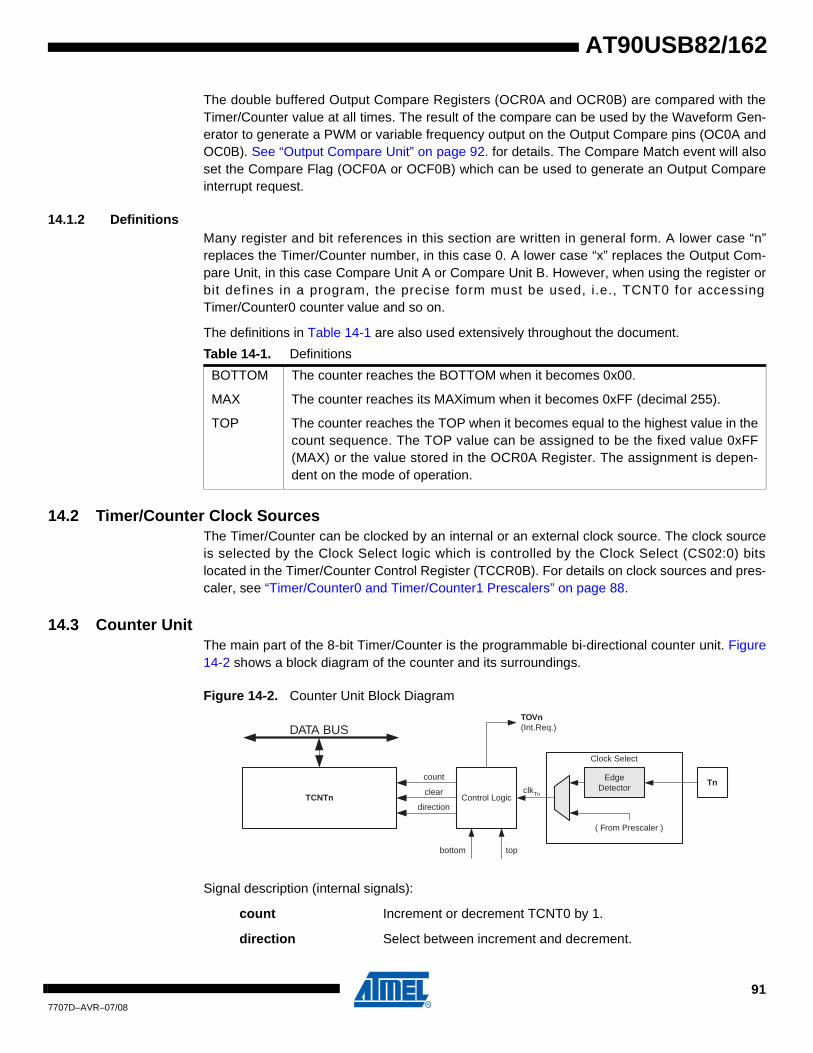
AT90USB82/162
The double buffered Output Compare Registers (OCR0A and OCR0B) are compared with the Timer/Counter value at all times. The result of the compare can be used by the Waveform Gen-erator to generate a PWM or variable frequency output on the Output Compare pins (OC0A and OC0B). See “Output Compare Unit” on page 92. for details. The Compare Match event will also set the Compare Flag (OCF0A or OCF0B) which can be used to generate an Output Compare interrupt request.
14.1.2 DefinitionsMany register and bit references in this section are written in general form. A lower case “n” replaces the Timer/Counter number, in this case 0. A lower case “x” replaces the Output Com-pare Unit, in this case Compare Unit A or Compare Unit B. However, when using the register or bit defines in a program, the precise form must be used, i.e., TCNT0 for accessing Timer/Counter0 counter value and so on.
The definitions in Table 14-1 are also used extensively throughout the document.
14.2 Timer/Counter Clock SourcesThe Timer/Counter can be clocked by an internal or an external clock source. The clock source is selected by the Clock Select logic which is controlled by the Clock Select (CS02:0) bits located in the Timer/Counter Control Register (TCCR0B). For details on clock sources and pres-caler, see “Timer/Counter0 and Timer/Counter1 Prescalers” on page 88.
14.3 Counter UnitThe main part of the 8-bit Timer/Counter is the programmable bi-directional counter unit. Figure 14-2 shows a block diagram of the counter and its surroundings.
Figure 14-2. Counter Unit Block Diagram
Signal description (internal signals):
count Increment or decrement TCNT0 by 1.
direction Select between increment and decrement.
Table 14-1. Definitions
BOTTOM The counter reaches the BOTTOM when it becomes 0x00.
MAX The counter reaches its MAXimum when it becomes 0xFF (decimal 255).
TOP The counter reaches the TOP when it becomes equal to the highest value in the count sequence. The TOP value can be assigned to be the fixed value 0xFF (MAX) or the value stored in the OCR0A Register. The assignment is depen-dent on the mode of operation.
DATA BUS
TCNTn Control Logic
count
TOVn(Int.Req.)
Clock Select
top
TnEdge
Detector
( From Prescaler )
clkTn
bottom
direction
clear
917707D–AVR–07/08

clear Clear TCNT0 (set all bits to zero).
clkTn Timer/Counter clock, referred to as clkT0 in the following.
top Signalize that TCNT0 has reached maximum value.
bottom Signalize that TCNT0 has reached minimum value (zero).
Depending of the mode of operation used, the counter is cleared, incremented, or decremented at each timer clock (clkT0). clkT0 can be generated from an external or internal clock source, selected by the Clock Select bits (CS02:0). When no clock source is selected (CS02:0 = 0) the timer is stopped. However, the TCNT0 value can be accessed by the CPU, regardless of whether clkT0 is present or not. A CPU write overrides (has priority over) all counter clear or count operations.
The counting sequence is determined by the setting of the WGM01 and WGM00 bits located in the Timer/Counter Control Register (TCCR0A) and the WGM02 bit located in the Timer/Counter Control Register B (TCCR0B). There are close connections between how the counter behaves (counts) and how waveforms are generated on the Output Compare outputs OC0A and OC0B. For more details about advanced counting sequences and waveform generation, see “Modes of Operation” on page 95.
The Timer/Counter Overflow Flag (TOV0) is set according to the mode of operation selected by the WGM02:0 bits. TOV0 can be used for generating a CPU interrupt.
14.4 Output Compare UnitThe 8-bit comparator continuously compares TCNT0 with the Output Compare Registers (OCR0A and OCR0B). Whenever TCNT0 equals OCR0A or OCR0B, the comparator signals a match. A match will set the Output Compare Flag (OCF0A or OCF0B) at the next timer clock cycle. If the corresponding interrupt is enabled, the Output Compare Flag generates an Output Compare interrupt. The Output Compare Flag is automatically cleared when the interrupt is exe-cuted. Alternatively, the flag can be cleared by software by writing a logical one to its I/O bit location. The Waveform Generator uses the match signal to generate an output according to operating mode set by the WGM02:0 bits and Compare Output mode (COM0x1:0) bits. The max and bottom signals are used by the Waveform Generator for handling the special cases of the extreme values in some modes of operation (“Modes of Operation” on page 95).
Figure 14-3 shows a block diagram of the Output Compare unit.
927707D–AVR–07/08
AT90USB82/162

AT90USB82/162
Figure 14-3. Output Compare Unit, Block Diagram
The OCR0x Registers are double buffered when using any of the Pulse Width Modulation (PWM) modes. For the normal and Clear Timer on Compare (CTC) modes of operation, the dou-ble buffering is disabled. The double buffering synchronizes the update of the OCR0x Compare Registers to either top or bottom of the counting sequence. The synchronization prevents the occurrence of odd-length, non-symmetrical PWM pulses, thereby making the output glitch-free.
The OCR0x Register access may seem complex, but this is not case. When the double buffering is enabled, the CPU has access to the OCR0x Buffer Register, and if double buffering is dis-abled the CPU will access the OCR0x directly.
14.4.1 Force Output CompareIn non-PWM waveform generation modes, the match output of the comparator can be forced by writing a one to the Force Output Compare (FOC0x) bit. Forcing Compare Match will not set the OCF0x Flag or reload/clear the timer, but the OC0x pin will be updated as if a real Compare Match had occurred (the COM0x1:0 bits settings define whether the OC0x pin is set, cleared or toggled).
14.4.2 Compare Match Blocking by TCNT0 WriteAll CPU write operations to the TCNT0 Register will block any Compare Match that occur in the next timer clock cycle, even when the timer is stopped. This feature allows OCR0x to be initial-ized to the same value as TCNT0 without triggering an interrupt when the Timer/Counter clock is enabled.
14.4.3 Using the Output Compare UnitSince writing TCNT0 in any mode of operation will block all Compare Matches for one timer clock cycle, there are risks involved when changing TCNT0 when using the Output Compare Unit, independently of whether the Timer/Counter is running or not. If the value written to TCNT0equals the OCR0x value, the Compare Match will be missed, resulting in incorrect waveform
OCFnx (Int.Req.)
= (8-bit Comparator )
OCRnx
OCnx
DATA BUS
TCNTn
WGMn1:0
Waveform Generator
top
FOCn
COMnX1:0
bottom
937707D–AVR–07/08

generation. Similarly, do not write the TCNT0 value equal to BOTTOM when the counter is down-counting.
The setup of the OC0x should be performed before setting the Data Direction Register for the port pin to output. The easiest way of setting the OC0x value is to use the Force Output Com-pare (FOC0x) strobe bits in Normal mode. The OC0x Registers keep their values even when changing between Waveform Generation modes.
Be aware that the COM0x1:0 bits are not double buffered together with the compare value. Changing the COM0x1:0 bits will take effect immediately.
14.5 Compare Match Output UnitThe Compare Output mode (COM0x1:0) bits have two functions. The Waveform Generator uses the COM0x1:0 bits for defining the Output Compare (OC0x) state at the next Compare Match. Also, the COM0x1:0 bits control the OC0x pin output source. Figure 14-4 shows a simplified schematic of the logic affected by the COM0x1:0 bit setting. The I/O Registers, I/O bits, and I/O pins in the figure are shown in bold. Only the parts of the general I/O Port Control Registers (DDR and PORT) that are affected by the COM0x1:0 bits are shown. When referring to the OC0x state, the reference is for the internal OC0x Register, not the OC0x pin. If a system reset occur, the OC0x Register is reset to “0”.
Figure 14-4. Compare Match Output Unit, Schematic
The general I/O port function is overridden by the Output Compare (OC0x) from the Waveform Generator if either of the COM0x1:0 bits are set. However, the OC0x pin direction (input or out-put) is still controlled by the Data Direction Register (DDR) for the port pin. The Data Direction Register bit for the OC0x pin (DDR_OC0x) must be set as output before the OC0x value is visi-ble on the pin. The port override function is independent of the Waveform Generation mode.
The design of the Output Compare pin logic allows initialization of the OC0x state before the out-put is enabled. Note that some COM0x1:0 bit settings are reserved for certain modes of operation. See “8-bit Timer/Counter Register Description” on page 100.
PORT
DDR
D Q
D Q
OCnxPinOCnx
D QWaveformGenerator
COMnx1
COMnx0
0
1
DAT
A B
US
FOCn
clkI/O
947707D–AVR–07/08
AT90USB82/162

AT90USB82/162
14.5.1 Compare Output Mode and Waveform GenerationThe Waveform Generator uses the COM0x1:0 bits differently in Normal, CTC, and PWM modes. For all modes, setting the COM0x1:0 = 0 tells the Waveform Generator that no action on the OC0x Register is to be performed on the next Compare Match. For compare output actions in the non-PWM modes refer to Table 14-2 on page 101. For fast PWM mode, refer to Table 14-3 on page 101, and for phase correct PWM refer to Table 14-4 on page 101.
A change of the COM0x1:0 bits state will have effect at the first Compare Match after the bits are written. For non-PWM modes, the action can be forced to have immediate effect by using the FOC0x strobe bits.
14.6 Modes of OperationThe mode of operation, i.e., the behavior of the Timer/Counter and the Output Compare pins, is defined by the combination of the Waveform Generation mode (WGM02:0) and Compare Output mode (COM0x1:0) bits. The Compare Output mode bits do not affect the counting sequence, while the Waveform Generation mode bits do. The COM0x1:0 bits control whether the PWM out-put generated should be inverted or not (inverted or non-inverted PWM). For non-PWM modes the COM0x1:0 bits control whether the output should be set, cleared, or toggled at a Compare Match (See “Compare Match Output Unit” on page 94.).
For detailed timing information see “Timer/Counter Timing Diagrams” on page 99.
14.6.1 Normal ModeThe simplest mode of operation is the Normal mode (WGM02:0 = 0). In this mode the counting direction is always up (incrementing), and no counter clear is performed. The counter simply overruns when it passes its maximum 8-bit value (TOP = 0xFF) and then restarts from the bot-tom (0x00). In normal operation the Timer/Counter Overflow Flag (TOV0) will be set in the same timer clock cycle as the TCNT0 becomes zero. The TOV0 Flag in this case behaves like a ninth bit, except that it is only set, not cleared. However, combined with the timer overflow interrupt that automatically clears the TOV0 Flag, the timer resolution can be increased by software. There are no special cases to consider in the Normal mode, a new counter value can be written anytime.
The Output Compare Unit can be used to generate interrupts at some given time. Using the Out-put Compare to generate waveforms in Normal mode is not recommended, since this will occupy too much of the CPU time.
14.6.2 Clear Timer on Compare Match (CTC) ModeIn Clear Timer on Compare or CTC mode (WGM02:0 = 2), the OCR0A Register is used to manipulate the counter resolution. In CTC mode the counter is cleared to zero when the counter value (TCNT0) matches the OCR0A. The OCR0A defines the top value for the counter, hence also its resolution. This mode allows greater control of the Compare Match output frequency. It also simplifies the operation of counting external events.
The timing diagram for the CTC mode is shown in Figure 14-5. The counter value (TCNT0) increases until a Compare Match occurs between TCNT0 and OCR0A, and then counter (TCNT0) is cleared.
957707D–AVR–07/08

Figure 14-5. CTC Mode, Timing Diagram
An interrupt can be generated each time the counter value reaches the TOP value by using the OCF0A Flag. If the interrupt is enabled, the interrupt handler routine can be used for updating the TOP value. However, changing TOP to a value close to BOTTOM when the counter is run-ning with none or a low prescaler value must be done with care since the CTC mode does not have the double buffering feature. If the new value written to OCR0A is lower than the current value of TCNT0, the counter will miss the Compare Match. The counter will then have to count to its maximum value (0xFF) and wrap around starting at 0x00 before the Compare Match can occur.
For generating a waveform output in CTC mode, the OC0A output can be set to toggle its logical level on each Compare Match by setting the Compare Output mode bits to toggle mode (COM0A1:0 = 1). The OC0A value will not be visible on the port pin unless the data direction for the pin is set to output. The waveform generated will have a maximum frequency of fOC0 = fclk_I/O/2 when OCR0A is set to zero (0x00). The waveform frequency is defined by the following equation:
The N variable represents the prescale factor (1, 8, 64, 256, or 1024).
As for the Normal mode of operation, the TOV0 Flag is set in the same timer clock cycle that the counter counts from MAX to 0x00.
14.6.3 Fast PWM ModeThe fast Pulse Width Modulation or fast PWM mode (WGM02:0 = 3 or 7) provides a high fre-quency PWM waveform generation option. The fast PWM differs from the other PWM option by its single-slope operation. The counter counts from BOTTOM to TOP then restarts from BOT-TOM. TOP is defined as 0xFF when WGM2:0 = 3, and OCR0A when WGM2:0 = 7. In non-inverting Compare Output mode, the Output Compare (OC0x) is cleared on the Compare Match between TCNT0 and OCR0x, and set at BOTTOM. In inverting Compare Output mode, the out-put is set on Compare Match and cleared at BOTTOM. Due to the single-slope operation, the operating frequency of the fast PWM mode can be twice as high as the phase correct PWM mode that use dual-slope operation. This high frequency makes the fast PWM mode well suited for power regulation, rectification, and DAC applications. High frequency allows physically small sized external components (coils, capacitors), and therefore reduces total system cost.
In fast PWM mode, the counter is incremented until the counter value matches the TOP value. The counter is then cleared at the following timer clock cycle. The timing diagram for the fast
TCNTn
OCn(Toggle)
OCnx Interrupt Flag Set
1 4Period 2 3
(COMnx1:0 = 1)
fOCnx
fclk_I/O
2 N 1 OCRnx+( )⋅ ⋅--------------------------------------------------=
967707D–AVR–07/08
AT90USB82/162

AT90USB82/162
PWM mode is shown in Figure 14-6. The TCNT0 value is in the timing diagram shown as a his-togram for illustrating the single-slope operation. The diagram includes non-inverted and inverted PWM outputs. The small horizontal line marks on the TCNT0 slopes represent Com-pare Matches between OCR0x and TCNT0.
Figure 14-6. Fast PWM Mode, Timing Diagram
The Timer/Counter Overflow Flag (TOV0) is set each time the counter reaches TOP. If the inter-rupt is enabled, the interrupt handler routine can be used for updating the compare value.
In fast PWM mode, the compare unit allows generation of PWM waveforms on the OC0x pins. Setting the COM0x1:0 bits to two will produce a non-inverted PWM and an inverted PWM output can be generated by setting the COM0x1:0 to three: Setting the COM0A1:0 bits to one allows the OC0A pin to toggle on Compare Matches if the WGM02 bit is set. This option is not available for the OC0B pin (See Table 14-3 on page 101). The actual OC0x value will only be visible on the port pin if the data direction for the port pin is set as output. The PWM waveform is gener-ated by setting (or clearing) the OC0x Register at the Compare Match between OCR0x and TCNT0, and clearing (or setting) the OC0x Register at the timer clock cycle the counter is cleared (changes from TOP to BOTTOM).
The PWM frequency for the output can be calculated by the following equation:
The N variable represents the prescale factor (1, 8, 64, 256, or 1024).
The extreme values for the OCR0A Register represents special cases when generating a PWM waveform output in the fast PWM mode. If the OCR0A is set equal to BOTTOM, the output will be a narrow spike for each MAX+1 timer clock cycle. Setting the OCR0A equal to MAX will result in a constantly high or low output (depending on the polarity of the output set by the COM0A1:0 bits.)
A frequency (with 50% duty cycle) waveform output in fast PWM mode can be achieved by set-ting OC0x to toggle its logical level on each Compare Match (COM0x1:0 = 1). The waveform generated will have a maximum frequency of fOC0 = fclk_I/O/2 when OCR0A is set to zero. This
TCNTn
OCRnx Update andTOVn Interrupt Flag Set
1Period 2 3
OCnx
OCnx
(COMnx1:0 = 2)
(COMnx1:0 = 3)
OCRnx Interrupt Flag Set
4 5 6 7
fOCnxPWM
fclk_I/O
N 256⋅------------------=
977707D–AVR–07/08

feature is similar to the OC0A toggle in CTC mode, except the double buffer feature of the Out-put Compare unit is enabled in the fast PWM mode.
14.6.4 Phase Correct PWM ModeThe phase correct PWM mode (WGM02:0 = 1 or 5) provides a high resolution phase correct PWM waveform generation option. The phase correct PWM mode is based on a dual-slope operation. The counter counts repeatedly from BOTTOM to TOP and then from TOP to BOT-TOM. TOP is defined as 0xFF when WGM2:0 = 1, and OCR0A when WGM2:0 = 5. In non-inverting Compare Output mode, the Output Compare (OC0x) is cleared on the Compare Match between TCNT0 and OCR0x while upcounting, and set on the Compare Match while down-counting. In inverting Output Compare mode, the operation is inverted. The dual-slope operation has lower maximum operation frequency than single slope operation. However, due to the sym-metric feature of the dual-slope PWM modes, these modes are preferred for motor control applications.
In phase correct PWM mode the counter is incremented until the counter value matches TOP. When the counter reaches TOP, it changes the count direction. The TCNT0 value will be equal to TOP for one timer clock cycle. The timing diagram for the phase correct PWM mode is shown on Figure 14-7. The TCNT0 value is in the timing diagram shown as a histogram for illustrating the dual-slope operation. The diagram includes non-inverted and inverted PWM outputs. The small horizontal line marks on the TCNT0 slopes represent Compare Matches between OCR0x and TCNT0.
Figure 14-7. Phase Correct PWM Mode, Timing Diagram
The Timer/Counter Overflow Flag (TOV0) is set each time the counter reaches BOTTOM. The Interrupt Flag can be used to generate an interrupt each time the counter reaches the BOTTOM value.
In phase correct PWM mode, the compare unit allows generation of PWM waveforms on the OC0x pins. Setting the COM0x1:0 bits to two will produce a non-inverted PWM. An inverted PWM output can be generated by setting the COM0x1:0 to three: Setting the COM0A0 bits to
TOVn Interrupt Flag Set
OCnx Interrupt Flag Set
1 2 3
TCNTn
Period
OCnx
OCnx
(COMnx1:0 = 2)
(COMnx1:0 = 3)
OCRnx Update
987707D–AVR–07/08
AT90USB82/162

AT90USB82/162
one allows the OC0A pin to toggle on Compare Matches if the WGM02 bit is set. This option is not available for the OC0B pin (See Table 14-4 on page 101). The actual OC0x value will only be visible on the port pin if the data direction for the port pin is set as output. The PWM wave-form is generated by clearing (or setting) the OC0x Register at the Compare Match between OCR0x and TCNT0 when the counter increments, and setting (or clearing) the OC0x Register at Compare Match between OCR0x and TCNT0 when the counter decrements. The PWM fre-quency for the output when using phase correct PWM can be calculated by the following equation:
The N variable represents the prescale factor (1, 8, 64, 256, or 1024).
The extreme values for the OCR0A Register represent special cases when generating a PWM waveform output in the phase correct PWM mode. If the OCR0A is set equal to BOTTOM, the output will be continuously low and if set equal to MAX the output will be continuously high for non-inverted PWM mode. For inverted PWM the output will have the opposite logic values.
At the very start of period 2 in Figure 14-7 OCnx has a transition from high to low even though there is no Compare Match. The point of this transition is to guarantee symmetry around BOT-TOM. There are two cases that give a transition without Compare Match.
• OCR0A changes its value from MAX, like in Figure 14-7. When the OCR0A value is MAX the OCn pin value is the same as the result of a down-counting Compare Match. To ensure symmetry around BOTTOM the OCn value at MAX must correspond to the result of an up-counting Compare Match.
• The timer starts counting from a value higher than the one in OCR0A, and for that reason misses the Compare Match and hence the OCn change that would have happened on the way up.
14.7 Timer/Counter Timing DiagramsThe Timer/Counter is a synchronous design and the timer clock (clkT0) is therefore shown as a clock enable signal in the following figures. The figures include information on when Interrupt Flags are set. Figure 14-8 contains timing data for basic Timer/Counter operation. The figure shows the count sequence close to the MAX value in all modes other than phase correct PWM mode.
Figure 14-8. Timer/Counter Timing Diagram, no Prescaling
Figure 14-9 shows the same timing data, but with the prescaler enabled.
fOCnxPCPWM
fclk_I/O
N 510⋅------------------=
clkTn(clkI/O/1)
TOVn
clkI/O
TCNTn MAX - 1 MAX BOTTOM BOTTOM + 1
997707D–AVR–07/08

Figure 14-9. Timer/Counter Timing Diagram, with Prescaler (fclk_I/O/8)
Figure 14-10 shows the setting of OCF0B in all modes and OCF0A in all modes except CTC mode and PWM mode, where OCR0A is TOP.
Figure 14-10. Timer/Counter Timing Diagram, Setting of OCF0x, with Prescaler (fclk_I/O/8)
Figure 14-11 shows the setting of OCF0A and the clearing of TCNT0 in CTC mode and fast PWM mode where OCR0A is TOP.
Figure 14-11. Timer/Counter Timing Diagram, Clear Timer on Compare Match mode, with Pres-caler (fclk_I/O/8)
14.8 8-bit Timer/Counter Register Description
14.8.1 Timer/Counter Control Register A – TCCR0A
TOVn
TCNTn MAX - 1 MAX BOTTOM BOTTOM + 1
clkI/O
clkTn(clkI/O/8)
OCFnx
OCRnx
TCNTn
OCRnx Value
OCRnx - 1 OCRnx OCRnx + 1 OCRnx + 2
clkI/O
clkTn(clkI/O/8)
OCFnx
OCRnx
TCNTn(CTC)
TOP
TOP - 1 TOP BOTTOM BOTTOM + 1
clkI/O
clkTn(clkI/O/8)
Bit 7 6 5 4 3 2 1 0
COM0A1 COM0A0 COM0B1 COM0B0 – – WGM01 WGM00 TCCR0A
Read/Write R/W R/W R/W R/W R R R/W R/W
1007707D–AVR–07/08
AT90USB82/162

AT90USB82/162
• Bits 7:6 – COM01A:0: Compare Match Output A ModeThese bits control the Output Compare pin (OC0A) behavior. If one or both of the COM0A1:0 bits are set, the OC0A output overrides the normal port functionality of the I/O pin it is connected to. However, note that the Data Direction Register (DDR) bit corresponding to the OC0A pin must be set in order to enable the output driver.
When OC0A is connected to the pin, the function of the COM0A1:0 bits depends on the WGM02:0 bit setting. Table 14-2 shows the COM0A1:0 bit functionality when the WGM02:0 bits are set to a normal or CTC mode (non-PWM).
Table 14-3 shows the COM0A1:0 bit functionality when the WGM01:0 bits are set to fast PWM mode.
Note: 1. A special case occurs when OCR0A equals TOP and COM0A1 is set. In this case, the Com-pare Match is ignored, but the set or clear is done at TOP. See “Fast PWM Mode” on page 96 for more details.
Table 14-4 shows the COM0A1:0 bit functionality when the WGM02:0 bits are set to phase cor-rect PWM mode.
Initial Value 0 0 0 0 0 0 0 0
Table 14-2. Compare Output Mode, non-PWM Mode
COM0A1 COM0A0 Description
0 0 Normal port operation, OC0A disconnected.
0 1 Toggle OC0A on Compare Match
1 0 Clear OC0A on Compare Match
1 1 Set OC0A on Compare Match
Table 14-3. Compare Output Mode, Fast PWM Mode(1)
COM0A1 COM0A0 Description
0 0 Normal port operation, OC0A disconnected.
0 1WGM02 = 0: Normal Port Operation, OC0A Disconnected. WGM02 = 1: Toggle OC0A on Compare Match.
1 0 Clear OC0A on Compare Match, set OC0A at TOP
1 1 Set OC0A on Compare Match, clear OC0A at TOP
Table 14-4. Compare Output Mode, Phase Correct PWM Mode(1)
COM0A1 COM0A0 Description
0 0 Normal port operation, OC0A disconnected.
0 1WGM02 = 0: Normal Port Operation, OC0A Disconnected. WGM02 = 1: Toggle OC0A on Compare Match.
1 0Clear OC0A on Compare Match when up-counting. Set OC0A on Compare Match when down-counting.
1 1Set OC0A on Compare Match when up-counting. Clear OC0A on Compare Match when down-counting.
1017707D–AVR–07/08

Note: 1. A special case occurs when OCR0A equals TOP and COM0A1 is set. In this case, the Com-pare Match is ignored, but the set or clear is done at TOP. See “Phase Correct PWM Mode” on page 98 for more details.
• Bits 5:4 – COM0B1:0: Compare Match Output B ModeThese bits control the Output Compare pin (OC0B) behavior. If one or both of the COM0B1:0 bits are set, the OC0B output overrides the normal port functionality of the I/O pin it is connected to. However, note that the Data Direction Register (DDR) bit corresponding to the OC0B pin must be set in order to enable the output driver.
When OC0B is connected to the pin, the function of the COM0B1:0 bits depends on the WGM02:0 bit setting. Table 14-2 shows the COM0A1:0 bit functionality when the WGM02:0 bits are set to a normal or CTC mode (non-PWM).
Table 14-3 shows the COM0B1:0 bit functionality when the WGM02:0 bits are set to fast PWM mode.
Note: 1. A special case occurs when OCR0B equals TOP and COM0B1 is set. In this case, the Com-pare Match is ignored, but the set or clear is done at TOP. See “Fast PWM Mode” on page 96 for more details.
Table 14-4 shows the COM0B1:0 bit functionality when the WGM02:0 bits are set to phase cor-rect PWM mode.
Table 14-5. Compare Output Mode, non-PWM Mode
COM01 COM00 Description
0 0 Normal port operation, OC0B disconnected.
0 1 Toggle OC0B on Compare Match
1 0 Clear OC0B on Compare Match
1 1 Set OC0B on Compare Match
Table 14-6. Compare Output Mode, Fast PWM Mode(1)
COM01 COM00 Description
0 0 Normal port operation, OC0B disconnected.
0 1 Reserved
1 0 Clear OC0B on Compare Match, set OC0B at TOP
1 1 Set OC0B on Compare Match, clear OC0B at TOP
Table 14-7. Compare Output Mode, Phase Correct PWM Mode(1)
COM0A1 COM0A0 Description
0 0 Normal port operation, OC0B disconnected.
0 1 Reserved
1 0Clear OC0B on Compare Match when up-counting. Set OC0B on Compare Match when down-counting.
1 1Set OC0B on Compare Match when up-counting. Clear OC0B on Compare Match when down-counting.
1027707D–AVR–07/08
AT90USB82/162

AT90USB82/162
Note: 1. A special case occurs when OCR0B equals TOP and COM0B1 is set. In this case, the Com-pare Match is ignored, but the set or clear is done at TOP. See “Phase Correct PWM Mode” on page 98 for more details.
• Bits 3, 2 – Res: Reserved BitsThese bits are reserved bits in the AT90USB82/162 and will always read as zero.
• Bits 1:0 – WGM01:0: Waveform Generation ModeCombined with the WGM02 bit found in the TCCR0B Register, these bits control the counting sequence of the counter, the source for maximum (TOP) counter value, and what type of wave-form generation to be used, see Table 14-8. Modes of operation supported by the Timer/Counter unit are: Normal mode (counter), Clear Timer on Compare Match (CTC) mode, and two types of Pulse Width Modulation (PWM) modes (see “Modes of Operation” on page 95).
Notes: 1. MAX = 0xFF
2. BOTTOM = 0x00
14.8.2 Timer/Counter Control Register B – TCCR0B
• Bit 7 – FOC0A: Force Output Compare AThe FOC0A bit is only active when the WGM bits specify a non-PWM mode.
However, for ensuring compatibility with future devices, this bit must be set to zero when TCCR0B is written when operating in PWM mode. When writing a logical one to the FOC0A bit, an immediate Compare Match is forced on the Waveform Generation unit. The OC0A output is changed according to its COM0A1:0 bits setting. Note that the FOC0A bit is implemented as a strobe. Therefore it is the value present in the COM0A1:0 bits that determines the effect of the forced compare.
Table 14-8. Waveform Generation Mode Bit Description
Mode WGM2 WGM1 WGM0
Timer/Counter Mode of Operation TOP
Update ofOCRx at
TOV FlagSet on(1)(2)
0 0 0 0 Normal 0xFF Immediate MAX
1 0 0 1PWM, Phase Correct
0xFF TOP BOTTOM
2 0 1 0 CTC OCRA Immediate MAX
3 0 1 1 Fast PWM 0xFF TOP MAX
4 1 0 0 Reserved – – –
5 1 0 1PWM, Phase Correct
OCRA TOP BOTTOM
6 1 1 0 Reserved – – –
7 1 1 1 Fast PWM OCRA TOP TOP
Bit 7 6 5 4 3 2 1 0
FOC0A FOC0B – – WGM02 CS02 CS01 CS00 TCCR0B
Read/Write W W R R R/W R/W R/W R/W
Initial Value 0 0 0 0 0 0 0 0
1037707D–AVR–07/08

A FOC0A strobe will not generate any interrupt, nor will it clear the timer in CTC mode using OCR0A as TOP.
The FOC0A bit is always read as zero.
• Bit 6 – FOC0B: Force Output Compare BThe FOC0B bit is only active when the WGM bits specify a non-PWM mode.
However, for ensuring compatibility with future devices, this bit must be set to zero when TCCR0B is written when operating in PWM mode. When writing a logical one to the FOC0B bit, an immediate Compare Match is forced on the Waveform Generation unit. The OC0B output is changed according to its COM0B1:0 bits setting. Note that the FOC0B bit is implemented as a strobe. Therefore it is the value present in the COM0B1:0 bits that determines the effect of the forced compare.
A FOC0B strobe will not generate any interrupt, nor will it clear the timer in CTC mode using OCR0B as TOP.
The FOC0B bit is always read as zero.
• Bits 5:4 – Res: Reserved BitsThese bits are reserved bits and will always read as zero.
• Bit 3 – WGM02: Waveform Generation ModeSee the description in the “Timer/Counter Control Register A – TCCR0A” on page 100.
• Bits 2:0 – CS02:0: Clock SelectThe three Clock Select bits select the clock source to be used by the Timer/Counter.
If external pin modes are used for the Timer/Counter0, transitions on the T0 pin will clock the counter even if the pin is configured as an output. This feature allows software control of the counting.
14.8.3 Timer/Counter Register – TCNT0
Table 14-9. Clock Select Bit Description
CS02 CS01 CS00 Description
0 0 0 No clock source (Timer/Counter stopped)
0 0 1 clkI/O/(No prescaling)
0 1 0 clkI/O/8 (From prescaler)
0 1 1 clkI/O/64 (From prescaler)
1 0 0 clkI/O/256 (From prescaler)
1 0 1 clkI/O/1024 (From prescaler)
1 1 0 External clock source on T0 pin. Clock on falling edge.
1 1 1 External clock source on T0 pin. Clock on rising edge.
Bit 7 6 5 4 3 2 1 0
TCNT0[7:0] TCNT0
Read/Write R/W R/W R/W R/W R/W R/W R/W R/W
Initial Value 0 0 0 0 0 0 0 0
1047707D–AVR–07/08
AT90USB82/162

AT90USB82/162
The Timer/Counter Register gives direct access, both for read and write operations, to the Timer/Counter unit 8-bit counter. Writing to the TCNT0 Register blocks (removes) the Compare Match on the following timer clock. Modifying the counter (TCNT0) while the counter is running, introduces a risk of missing a Compare Match between TCNT0 and the OCR0x Registers.
14.8.4 Output Compare Register A – OCR0A
The Output Compare Register A contains an 8-bit value that is continuously compared with the counter value (TCNT0). A match can be used to generate an Output Compare interrupt, or to generate a waveform output on the OC0A pin.
14.8.5 Output Compare Register B – OCR0B
The Output Compare Register B contains an 8-bit value that is continuously compared with the counter value (TCNT0). A match can be used to generate an Output Compare interrupt, or to generate a waveform output on the OC0B pin.
14.8.6 Timer/Counter Interrupt Mask Register – TIMSK0
• Bits 7..3 – Res: Reserved BitsThese bits are reserved bits and will always read as zero.
• Bit 2 – OCIE0B: Timer/Counter Output Compare Match B Interrupt EnableWhen the OCIE0B bit is written to one, and the I-bit in the Status Register is set, the Timer/Counter Compare Match B interrupt is enabled. The corresponding interrupt is executed if a Compare Match in Timer/Counter occurs, i.e., when the OCF0B bit is set in the Timer/Counter Interrupt Flag Register – TIFR0.
• Bit 1 – OCIE0A: Timer/Counter0 Output Compare Match A Interrupt EnableWhen the OCIE0A bit is written to one, and the I-bit in the Status Register is set, the Timer/Counter0 Compare Match A interrupt is enabled. The corresponding interrupt is executed if a Compare Match in Timer/Counter0 occurs, i.e., when the OCF0A bit is set in the Timer/Counter 0 Interrupt Flag Register – TIFR0.
• Bit 0 – TOIE0: Timer/Counter0 Overflow Interrupt EnableWhen the TOIE0 bit is written to one, and the I-bit in the Status Register is set, the Timer/Counter0 Overflow interrupt is enabled. The corresponding interrupt is executed if an overflow in Timer/Counter0 occurs, i.e., when the TOV0 bit is set in the Timer/Counter 0 Inter-rupt Flag Register – TIFR0.
Bit 7 6 5 4 3 2 1 0
OCR0A[7:0] OCR0A
Read/Write R/W R/W R/W R/W R/W R/W R/W R/W
Initial Value 0 0 0 0 0 0 0 0
Bit 7 6 5 4 3 2 1 0
OCR0B[7:0] OCR0B
Read/Write R/W R/W R/W R/W R/W R/W R/W R/W
Initial Value 0 0 0 0 0 0 0 0
Bit 7 6 5 4 3 2 1 0
– – – – – OCIE0B OCIE0A TOIE0 TIMSK0
Read/Write R R R R R R/W R/W R/W
Initial Value 0 0 0 0 0 0 0 0
1057707D–AVR–07/08

14.8.7 Timer/Counter 0 Interrupt Flag Register – TIFR0
• Bits 7..3 – Res: Reserved BitsThese bits are reserved bits in the AT90USB82/162 and will always read as zero.
• Bit 2 – OCF0B: Timer/Counter 0 Output Compare B Match FlagThe OCF0B bit is set when a Compare Match occurs between the Timer/Counter and the data in OCR0B – Output Compare Register0 B. OCF0B is cleared by hardware when executing the cor-responding interrupt handling vector. Alternatively, OCF0B is cleared by writing a logic one to the flag. When the I-bit in SREG, OCIE0B (Timer/Counter Compare B Match Interrupt Enable), and OCF0B are set, the Timer/Counter Compare Match Interrupt is executed.
• Bit 1 – OCF0A: Timer/Counter 0 Output Compare A Match FlagThe OCF0A bit is set when a Compare Match occurs between the Timer/Counter0 and the data in OCR0A – Output Compare Register0. OCF0A is cleared by hardware when executing the cor-responding interrupt handling vector. Alternatively, OCF0A is cleared by writing a logic one to the flag. When the I-bit in SREG, OCIE0A (Timer/Counter0 Compare Match Interrupt Enable), and OCF0A are set, the Timer/Counter0 Compare Match Interrupt is executed.
• Bit 0 – TOV0: Timer/Counter0 Overflow FlagThe bit TOV0 is set when an overflow occurs in Timer/Counter0. TOV0 is cleared by hardware when executing the corresponding interrupt handling vector. Alternatively, TOV0 is cleared by writing a logic one to the flag. When the SREG I-bit, TOIE0 (Timer/Counter0 Overflow Interrupt Enable), and TOV0 are set, the Timer/Counter0 Overflow interrupt is executed.
The setting of this flag is dependent of the WGM02:0 bit setting. Refer to Table 14-8, “Waveform Generation Mode Bit Description” on page 103.
Bit 7 6 5 4 3 2 1 0
– – – – – OCF0B OCF0A TOV0 TIFR0
Read/Write R R R R R R/W R/W R/W
Initial Value 0 0 0 0 0 0 0 0
1067707D–AVR–07/08
AT90USB82/162

AT90USB82/162
15. 16-bit Timer/Counter 1 with PWMThe 16-bit Timer/Counter 1 unit allows accurate program execution timing (event management), wave generation, and signal timing measurement. The main features are:
• True 16-bit Design (i.e., Allows 16-bit PWM)• Three independent Output Compare Units• Double Buffered Output Compare Registers• One Input Capture Unit• Input Capture Noise Canceler• Clear Timer on Compare Match (Auto Reload)• Glitch-free, Phase Correct Pulse Width Modulator (PWM)• Variable PWM Period• Frequency Generator• External Event Counter• Five independent interrupt sources (TOV1, OCF1A, OCF1B, OCF1C, ICF1)
15.1 OverviewMost register and bit references in this section are written in general form. A lower case “n” replaces the Timer/Counter number (for this product, only n=1 is available), and a lower case “x” replaces the Output Compare unit channel. However, when using the register or bit defines in a program, the precise form must be used, i.e., TCNT1 for accessing Timer/Counter1 counter value and so on.
A simplified block diagram of the 16-bit Timer/Counter is shown in Figure 15-1. For the actual placement of I/O pins, see “Pinout AT90USB82/162” on page 3. CPU accessible I/O Registers, including I/O bits and I/O pins, are shown in bold. The device-specific I/O Register and bit loca-tions are listed in the “16-bit Timer/Counter 1 with PWM” on page 107.
The Power Reduction Timer/Counter1 bit, PRTIM1, in “Power Reduction Register 0 - PRR0” on page 43 must be written to zero to enable Timer/Counter1 module.
1077707D–AVR–07/08

Figure 15-1. 16-bit Timer/Counter Block Diagram(1)
Note: 1. Refer to Figure 1-1 on page 3, Table 11-3 on page 74, and Table 11-6 on page 77 for Timer/Counter1 pin placement and description.
15.1.1 RegistersThe Timer/Counter (TCNTn), Output Compare Registers (OCRnA/B/C), and Input Capture Reg-ister (ICRn) are all 16-bit registers. Special procedures must be followed when accessing the 16-bit registers. These procedures are described in the section “Accessing 16-bit Registers” on page 109. The Timer/Counter Control Registers (TCCRnA/B/C) are 8-bit registers and have no CPU access restrictions. Interrupt requests (shorten as Int.Req.) signals are all visible in the Timer Interrupt Flag Register (TIFRn). All interrupts are individually masked with the Timer Inter-rupt Mask Register (TIMSKn). TIFRn and TIMSKn are not shown in the figure since these registers are shared by other timer units.
The Timer/Counter can be clocked internally, via the prescaler, or by an external clock source on the Tn pin. The Clock Select logic block controls which clock source and edge the Timer/Counter uses to increment (or decrement) its value. The Timer/Counter is inactive when no clock source is selected. The output from the clock select logic is referred to as the timer clock (clkTn).
The double buffered Output Compare Registers (OCRnA/B/C) are compared with the Timer/Counter value at all time. The result of the compare can be used by the Waveform Gener-ator to generate a PWM or variable frequency output on the Output Compare pin (OCnA/B/C).
ICFn (Int.Req.)
TOVn
(Int.Req.)
Clock Select
Timer/Counter
DA
TA
BU
S
ICRn
=
=
=
TCNTn
WaveformGeneration
WaveformGeneration
WaveformGeneration
OCnA
OCnB
OCnC
NoiseCanceler
ICPn
=
FixedTOP
Values
EdgeDetector
Control Logic
= 0
TOP BOTTOM
Count
Clear
Direction
OCFnA
(Int.Req.)
OCFnB
(Int.Req.)
OCFnC
(Int.Req.)
TCCRnA TCCRnB TCCRnC
( From AnalogComparator Ouput )
TnEdge
Detector
( From Prescaler )
TCLK
OCRnC
OCRnB
OCRnA
1087707D–AVR–07/08
AT90USB82/162
AT90USB82/162
See “Output Compare Units” on page 116.. The compare match event will also set the Compare Match Flag (OCFnA/B/C) which can be used to generate an Output Compare interrupt request.
The Input Capture Register can capture the Timer/Counter value at a given external (edge trig-gered) event on either the Input Capture pin (ICPn) or on the Analog Comparator pins (See “Analog Comparator” on page 223.) The Input Capture unit includes a digital filtering unit (Noise Canceler) for reducing the chance of capturing noise spikes.
The TOP value, or maximum Timer/Counter value, can in some modes of operation be defined by either the OCRnA Register, the ICRn Register, or by a set of fixed values. When using OCRnA as TOP value in a PWM mode, the OCRnA Register can not be used for generating a PWM output. However, the TOP value will in this case be double buffered allowing the TOP value to be changed in run time. If a fixed TOP value is required, the ICRn Register can be used as an alternative, freeing the OCRnA to be used as PWM output.
15.1.2 DefinitionsThe following definitions are used extensively throughout the document:
15.2 Accessing 16-bit RegistersThe TCNTn, OCRnA/B/C, and ICRn are 16-bit registers that can be accessed by the AVR CPU via the 8-bit data bus. The 16-bit register must be byte accessed using two read or write opera-tions. Each 16-bit timer has a single 8-bit register for temporary storing of the high byte of the 16-bit access. The same Temporary Register is shared between all 16-bit registers within each 16-bit timer. Accessing the low byte triggers the 16-bit read or write operation. When the low byte of a 16-bit register is written by the CPU, the high byte stored in the Temporary Register, and the low byte written are both copied into the 16-bit register in the same clock cycle. When the low byte of a 16-bit register is read by the CPU, the high byte of the 16-bit register is copied into the Temporary Register in the same clock cycle as the low byte is read.
Not all 16-bit accesses uses the Temporary Register for the high byte. Reading the OCRnA/B/C16-bit registers does not involve using the Temporary Register.
To do a 16-bit write, the high byte must be written before the low byte. For a 16-bit read, the low byte must be read before the high byte.
The following code examples show how to access the 16-bit timer registers assuming that no interrupts updates the temporary register. The same principle can be used directly for accessing the OCRnA/B/C and ICRn Registers. Note that when using “C”, the compiler handles the 16-bit access.
BOTTOM The counter reaches the BOTTOM when it becomes 0x0000.
MAX The counter reaches its MAXimum when it becomes 0xFFFF (decimal 65535).
TOP
The counter reaches the TOP when it becomes equal to the highest value in the count sequence. The TOP value can be assigned to be one of the fixed values: 0x00FF, 0x01FF, or 0x03FF, or to the value stored in the OCRnA or ICRn Register. The assignment is dependent of the mode of operation.
1097707D–AVR–07/08

Note: 1. See “About Code Examples” on page 7.
The assembly code example returns the TCNTn value in the r17:r16 register pair.
It is important to notice that accessing 16-bit registers are atomic operations. If an interrupt occurs between the two instructions accessing the 16-bit register, and the interrupt code updates the temporary register by accessing the same or any other of the 16-bit Timer Regis-ters, then the result of the access outside the interrupt will be corrupted. Therefore, when both the main code and the interrupt code update the temporary register, the main code must disable the interrupts during the 16-bit access.
The following code examples show how to do an atomic read of the TCNTn Register contents. Reading any of the OCRnA/B/C or ICRn Registers can be done by using the same principle.
Assembly Code Examples(1)
...
; Set TCNTn to 0x01FF
ldi r17,0x01
ldi r16,0xFF
out TCNTnH,r17
out TCNTnL,r16
; Read TCNTn into r17:r16
in r16,TCNTnL
in r17,TCNTnH
...
C Code Examples(1)
unsigned int i;
...
/* Set TCNTn to 0x01FF */
TCNTn = 0x1FF;
/* Read TCNTn into i */
i = TCNTn;
...
1107707D–AVR–07/08
AT90USB82/162

AT90USB82/162
Note: 1. See “About Code Examples” on page 7.
The assembly code example returns the TCNTn value in the r17:r16 register pair.
Assembly Code Example(1)
TIM16_ReadTCNTn:
; Save global interrupt flag
in r18,SREG
; Disable interrupts
cli
; Read TCNTn into r17:r16
in r16,TCNTnL
in r17,TCNTnH
; Restore global interrupt flag
out SREG,r18
ret
C Code Example(1)
unsigned int TIM16_ReadTCNTn( void )
{
unsigned char sreg;
unsigned int i;
/* Save global interrupt flag */
sreg = SREG;
/* Disable interrupts */
__disable_interrupt();
/* Read TCNTn into i */
i = TCNTn;
/* Restore global interrupt flag */
SREG = sreg;
return i;
}
1117707D–AVR–07/08

The following code examples show how to do an atomic write of the TCNTn Register contents. Writing any of the OCRnA/B/C or ICRn Registers can be done by using the same principle.
Note: 1. See “About Code Examples” on page 7.
The assembly code example requires that the r17:r16 register pair contains the value to be writ-ten to TCNTn.
15.2.1 Reusing the Temporary High Byte RegisterIf writing to more than one 16-bit register where the high byte is the same for all registers written, then the high byte only needs to be written once. However, note that the same rule of atomic operation described previously also applies in this case.
15.3 Timer/Counter Clock SourcesThe Timer/Counter can be clocked by an internal or an external clock source. The clock source is selected by the Clock Select logic which is controlled by the Clock Select (CSn2:0) bits located in the Timer/Counter control Register B (TCCRnB). For details on clock sources and prescaler, see “Timer/Counter0 and Timer/Counter1 Prescalers” on page 88.
Assembly Code Example(1)
TIM16_WriteTCNTn:
; Save global interrupt flag
in r18,SREG
; Disable interrupts
cli
; Set TCNTn to r17:r16
out TCNTnH,r17
out TCNTnL,r16
; Restore global interrupt flag
out SREG,r18
ret
C Code Example(1)
void TIM16_WriteTCNTn( unsigned int i )
{
unsigned char sreg;
unsigned int i;
/* Save global interrupt flag */
sreg = SREG;
/* Disable interrupts */
__disable_interrupt();
/* Set TCNTn to i */
TCNTn = i;
/* Restore global interrupt flag */
SREG = sreg;
}
1127707D–AVR–07/08
AT90USB82/162

AT90USB82/162
15.4 Counter UnitThe main part of the 16-bit Timer/Counter is the programmable 16-bit bi-directional counter unit. Figure 15-2 shows a block diagram of the counter and its surroundings.
Figure 15-2. Counter Unit Block Diagram
Signal description (internal signals):
Count Increment or decrement TCNTn by 1.
Direction Select between increment and decrement.
Clear Clear TCNTn (set all bits to zero).
clkTn Timer/Counter clock.
TOP Signalize that TCNTn has reached maximum value.
BOTTOM Signalize that TCNTn has reached minimum value (zero).
The 16-bit counter is mapped into two 8-bit I/O memory locations: Counter High (TCNTnH) con-taining the upper eight bits of the counter, and Counter Low (TCNTnL) containing the lower eight bits. The TCNTnH Register can only be indirectly accessed by the CPU. When the CPU does an access to the TCNTnH I/O location, the CPU accesses the high byte temporary register (TEMP). The temporary register is updated with the TCNTnH value when the TCNTnL is read, and TCNTnH is updated with the temporary register value when TCNTnL is written. This allows the CPU to read or write the entire 16-bit counter value within one clock cycle via the 8-bit data bus. It is important to notice that there are special cases of writing to the TCNTn Register when the counter is counting that will give unpredictable results. The special cases are described in the sections where they are of importance.
Depending on the mode of operation used, the counter is cleared, incremented, or decremented at each timer clock (clkTn). The clkTn can be generated from an external or internal clock source, selected by the Clock Select bits (CSn2:0). When no clock source is selected (CSn2:0 = 0) the timer is stopped. However, the TCNTn value can be accessed by the CPU, independent of whether clkTn is present or not. A CPU write overrides (has priority over) all counter clear or count operations.
The counting sequence is determined by the setting of the Waveform Generation mode bits (WGMn3:0) located in the Timer/Counter Control Registers A and B (TCCRnA and TCCRnB). There are close connections between how the counter behaves (counts) and how waveforms are generated on the Output Compare outputs OCnx. For more details about advanced counting sequences and waveform generation, see “Modes of Operation” on page 119.
TEMP (8-bit)
DATA BUS (8-bit)
TCNTn (16-bit Counter)
TCNTnH (8-bit) TCNTnL (8-bit)Control Logic
Count
Clear
Direction
TOVn(Int.Req.)
Clock Select
TOP BOTTOM
TnEdge
Detector
( From Prescaler )
clkTn
1137707D–AVR–07/08

The Timer/Counter Overflow Flag (TOVn) is set according to the mode of operation selected by the WGMn3:0 bits. TOVn can be used for generating a CPU interrupt.
15.5 Input Capture UnitThe Timer/Counter incorporates an input capture unit that can capture external events and give them a time-stamp indicating time of occurrence. The external signal indicating an event, or mul-tiple events, can be applied via the ICPn pin or alternatively, for the Timer/Counter1 only, via the Analog Comparator unit. The time-stamps can then be used to calculate frequency, duty-cycle, and other features of the signal applied. Alternatively the time-stamps can be used for creating a log of the events.
The Input Capture unit is illustrated by the block diagram shown in Figure 15-3. The elements of the block diagram that are not directly a part of the input capture unit are gray shaded. The small “n” in register and bit names indicates the Timer/Counter number.
Figure 15-3. Input Capture Unit Block Diagram
Note: The Analog Comparator Output (ACO) can only trigger the Timer/Counter1 ICP – not Timer/Counter3, 4 or 5.
When a change of the logic level (an event) occurs on the Input Capture Pin (ICPn), alternatively on the analog Comparator output (ACO), and this change confirms to the setting of the edge detector, a capture will be triggered. When a capture is triggered, the 16-bit value of the counter (TCNTn) is written to the Input Capture Register (ICRn). The Input Capture Flag (ICFn) is set at the same system clock as the TCNTn value is copied into ICRn Register. If enabled (TICIEn = 1), the input capture flag generates an input capture interrupt. The ICFn flag is automatically cleared when the interrupt is executed. Alternatively the ICFn flag can be cleared by software by writing a logical one to its I/O bit location.
ICFn (Int.Req.)
AnalogComparator
WRITE ICRn (16-bit Register)
ICRnH (8-bit)
NoiseCanceler
ICPn
EdgeDetector
TEMP (8-bit)
DATA BUS (8-bit)
ICRnL (8-bit)
TCNTn (16-bit Counter)
TCNTnH (8-bit) TCNTnL (8-bit)
ACIC* ICNC ICESACO*
1147707D–AVR–07/08
AT90USB82/162

AT90USB82/162
Reading the 16-bit value in the Input Capture Register (ICRn) is done by first reading the low byte (ICRnL) and then the high byte (ICRnH). When the low byte is read the high byte is copied into the high byte Temporary Register (TEMP). When the CPU reads the ICRnH I/O location it will access the TEMP Register.
The ICRn Register can only be written when using a Waveform Generation mode that utilizes the ICRn Register for defining the counter’s TOP value. In these cases the Waveform Genera-tion mode (WGMn3:0) bits must be set before the TOP value can be written to the ICRnRegister. When writing the ICRn Register the high byte must be written to the ICRnH I/O location before the low byte is written to ICRnL.
For more information on how to access the 16-bit registers refer to “Accessing 16-bit Registers” on page 109.
15.5.1 Input Capture Trigger SourceThe main trigger source for the input capture unit is the Input Capture Pin (ICPn). Timer/Counter1 can alternatively use the analog comparator output as trigger source for the input capture unit. The Analog Comparator is selected as trigger source by setting the analog Comparator Input Capture (ACIC) bit in the Analog Comparator Control and Status Register(ACSR). Be aware that changing trigger source can trigger a capture. The input capture flag must therefore be cleared after the change.
Both the Input Capture Pin (ICPn) and the Analog Comparator output (ACO) inputs are sampled using the same technique as for the Tn pin (Figure 13-1 on page 88). The edge detector is also identical. However, when the noise canceler is enabled, additional logic is inserted before the edge detector, which increases the delay by four system clock cycles. Note that the input of the noise canceler and edge detector is always enabled unless the Timer/Counter is set in a Wave-form Generation mode that uses ICRn to define TOP.
An input capture can be triggered by software by controlling the port of the ICPn pin.
15.5.2 Noise CancelerThe noise canceler improves noise immunity by using a simple digital filtering scheme. The noise canceler input is monitored over four samples, and all four must be equal for changing the output that in turn is used by the edge detector.
The noise canceler is enabled by setting the Input Capture Noise Canceler (ICNCn) bit in Timer/Counter Control Register B (TCCRnB). When enabled the noise canceler introduces addi-tional four system clock cycles of delay from a change applied to the input, to the update of the ICRn Register. The noise canceler uses the system clock and is therefore not affected by the prescaler.
15.5.3 Using the Input Capture UnitThe main challenge when using the Input Capture unit is to assign enough processor capacity for handling the incoming events. The time between two events is critical. If the processor has not read the captured value in the ICRn Register before the next event occurs, the ICRn will be overwritten with a new value. In this case the result of the capture will be incorrect.
When using the Input Capture interrupt, the ICRn Register should be read as early in the inter-rupt handler routine as possible. Even though the Input Capture interrupt has relatively high priority, the maximum interrupt response time is dependent on the maximum number of clock cycles it takes to handle any of the other interrupt requests.
1157707D–AVR–07/08

Using the Input Capture unit in any mode of operation when the TOP value (resolution) is actively changed during operation, is not recommended.
Measurement of an external signal’s duty cycle requires that the trigger edge is changed after each capture. Changing the edge sensing must be done as early as possible after the ICRnRegister has been read. After a change of the edge, the Input Capture Flag (ICFn) must be cleared by software (writing a logical one to the I/O bit location). For measuring frequency only, the clearing of the ICFn Flag is not required (if an interrupt handler is used).
15.6 Output Compare UnitsThe 16-bit comparator continuously compares TCNTn with the Output Compare Register(OCRnx). If TCNT equals OCRnx the comparator signals a match. A match will set the Output Compare Flag (OCFnx) at the next timer clock cycle. If enabled (OCIEnx = 1), the Output Com-pare Flag generates an Output Compare interrupt. The OCFnx Flag is automatically cleared when the interrupt is executed. Alternatively the OCFnx Flag can be cleared by software by writ-ing a logical one to its I/O bit location. The Waveform Generator uses the match signal to generate an output according to operating mode set by the Waveform Generation mode(WGMn3:0) bits and Compare Output mode (COMnx1:0) bits. The TOP and BOTTOM signals are used by the Waveform Generator for handling the special cases of the extreme values in some modes of operation (See “Modes of Operation” on page 119.)
A special feature of Output Compare unit A allows it to define the Timer/Counter TOP value (i.e., counter resolution). In addition to the counter resolution, the TOP value defines the period time for waveforms generated by the Waveform Generator.
Figure 15-4 shows a block diagram of the Output Compare unit. The small “n” in the register and bit names indicates the device number (n = n for Timer/Counter n), and the “x” indicates Output Compare unit (A/B/C). The elements of the block diagram that are not directly a part of the Out-put Compare unit are gray shaded.
Figure 15-4. Output Compare Unit, Block Diagram
OCFnx (Int.Req.)
= (16-bit Comparator )
OCRnx Buffer (16-bit Register)
OCRnxH Buf. (8-bit)
OCnx
TEMP (8-bit)
DATA BUS (8-bit)
OCRnxL Buf. (8-bit)
TCNTn (16-bit Counter)
TCNTnH (8-bit) TCNTnL (8-bit)
COMnx1:0WGMn3:0
OCRnx (16-bit Register)
OCRnxH (8-bit) OCRnxL (8-bit)
Waveform GeneratorTOP
BOTTOM
1167707D–AVR–07/08
AT90USB82/162

AT90USB82/162
The OCRnx Register is double buffered when using any of the twelve Pulse Width Modulation(PWM) modes. For the Normal and Clear Timer on Compare (CTC) modes of operation, the double buffering is disabled. The double buffering synchronizes the update of the OCRnx Com-pare Register to either TOP or BOTTOM of the counting sequence. The synchronization prevents the occurrence of odd-length, non-symmetrical PWM pulses, thereby making the out-put glitch-free.
The OCRnx Register access may seem complex, but this is not case. When the double buffering is enabled, the CPU has access to the OCRnx Buffer Register, and if double buffering is dis-abled the CPU will access the OCRnx directly. The content of the OCR1x (Buffer or Compare) Register is only changed by a write operation (the Timer/Counter does not update this register automatically as the TCNT1 and ICR1 Register). Therefore OCR1x is not read via the high byte temporary register (TEMP). However, it is a good practice to read the low byte first as when accessing other 16-bit registers. Writing the OCRnx Registers must be done via the TEMP Reg-ister since the compare of all 16 bits is done continuously. The high byte (OCRnxH) has to be written first. When the high byte I/O location is written by the CPU, the TEMP Register will be updated by the value written. Then when the low byte (OCRnxL) is written to the lower eight bits, the high byte will be copied into the upper 8-bits of either the OCRnx buffer or OCRnx Compare Register in the same system clock cycle.
For more information of how to access the 16-bit registers refer to “Accessing 16-bit Registers” on page 109.
15.6.1 Force Output CompareIn non-PWM Waveform Generation modes, the match output of the comparator can be forced by writing a one to the Force Output Compare (FOCnx) bit. Forcing compare match will not set the OCFnx Flag or reload/clear the timer, but the OCnx pin will be updated as if a real compare match had occurred (the COMn1:0 bits settings define whether the OCnx pin is set, cleared or toggled).
15.6.2 Compare Match Blocking by TCNTn WriteAll CPU writes to the TCNTn Register will block any compare match that occurs in the next timer clock cycle, even when the timer is stopped. This feature allows OCRnx to be initialized to the same value as TCNTn without triggering an interrupt when the Timer/Counter clock is enabled.
15.6.3 Using the Output Compare UnitSince writing TCNTn in any mode of operation will block all compare matches for one timer clock cycle, there are risks involved when changing TCNTn when using any of the Output Compare channels, independent of whether the Timer/Counter is running or not. If the value written to TCNTn equals the OCRnx value, the compare match will be missed, resulting in incorrect wave-form generation. Do not write the TCNTn equal to TOP in PWM modes with variable TOP values. The compare match for the TOP will be ignored and the counter will continue to 0xFFFF. Similarly, do not write the TCNTn value equal to BOTTOM when the counter is downcounting.
The setup of the OCnx should be performed before setting the Data Direction Register for the port pin to output. The easiest way of setting the OCnx value is to use the Force Output Com-pare (FOCnx) strobe bits in Normal mode. The OCnx Register keeps its value even when changing between Waveform Generation modes.
Be aware that the COMnx1:0 bits are not double buffered together with the compare value. Changing the COMnx1:0 bits will take effect immediately.
1177707D–AVR–07/08

15.7 Compare Match Output UnitThe Compare Output mode (COMnx1:0) bits have two functions. The Waveform Generator uses the COMnx1:0 bits for defining the Output Compare (OCnx) state at the next compare match. Secondly the COMnx1:0 bits control the OCnx pin output source. Figure 15-5 shows a simplified schematic of the logic affected by the COMnx1:0 bit setting. The I/O Registers, I/O bits, and I/O pins in the figure are shown in bold. Only the parts of the general I/O Port Control Registers (DDR and PORT) that are affected by the COMnx1:0 bits are shown. When referring to the OCnx state, the reference is for the internal OCnx Register, not the OCnx pin. If a system reset occur, the OCnx Register is reset to “0”.
Figure 15-5. Compare Match Output Unit, Schematic
The general I/O port function is overridden by the Output Compare (OCnx) from the Waveform Generator if either of the COMnx1:0 bits are set. However, the OCnx pin direction (input or out-put) is still controlled by the Data Direction Register (DDR) for the port pin. The Data Direction Register bit for the OCnx pin (DDR_OCnx) must be set as output before the OCnx value is visi-ble on the pin. The port override function is generally independent of the Waveform Generation mode, but there are some exceptions. Refer to Table 15-1, Table 15-2 and Table 15-3 for details.
The design of the Output Compare pin logic allows initialization of the OCnx state before the out-put is enabled. Note that some COMnx1:0 bit settings are reserved for certain modes of operation. See “16-bit Timer/Counter 1 with PWM” on page 107.
The COMnx1:0 bits have no effect on the Input Capture unit.
15.7.1 Compare Output Mode and Waveform GenerationThe Waveform Generator uses the COMnx1:0 bits differently in normal, CTC, and PWM modes. For all modes, setting the COMnx1:0 = 0 tells the Waveform Generator that no action on the OCnx Register is to be performed on the next compare match. For compare output actions in the
PORT
DDR
D Q
D Q
OCnxPinOCnx
D QWaveformGenerator
COMnx1
COMnx0
0
1D
ATA
BU
S
FOCnx
clkI/O
1187707D–AVR–07/08
AT90USB82/162

AT90USB82/162
non-PWM modes refer to Table 15-1 on page 129. For fast PWM mode refer to Table 15-2 on page 129, and for phase correct and phase and frequency correct PWM refer to Table 15-3 on page 130.
A change of the COMnx1:0 bits state will have effect at the first compare match after the bits are written. For non-PWM modes, the action can be forced to have immediate effect by using the FOCnx strobe bits.
15.8 Modes of OperationThe mode of operation, i.e., the behavior of the Timer/Counter and the Output Compare pins, is defined by the combination of the Waveform Generation mode (WGMn3:0) and Compare Output mode (COMnx1:0) bits. The Compare Output mode bits do not affect the counting sequence, while the Waveform Generation mode bits do. The COMnx1:0 bits control whether the PWM out-put generated should be inverted or not (inverted or non-inverted PWM). For non-PWM modes the COMnx1:0 bits control whether the output should be set, cleared or toggle at a compare match (See “Compare Match Output Unit” on page 118.)
For detailed timing information refer to “Timer/Counter Timing Diagrams” on page 126.
15.8.1 Normal ModeThe simplest mode of operation is the Normal mode (WGMn3:0 = 0). In this mode the counting direction is always up (incrementing), and no counter clear is performed. The counter simply overruns when it passes its maximum 16-bit value (MAX = 0xFFFF) and then restarts from the BOTTOM (0x0000). In normal operation the Timer/Counter Overflow Flag (TOVn) will be set in the same timer clock cycle as the TCNTn becomes zero. The TOVn Flag in this case behaves like a 17th bit, except that it is only set, not cleared. However, combined with the timer overflow interrupt that automatically clears the TOVn Flag, the timer resolution can be increased by soft-ware. There are no special cases to consider in the Normal mode, a new counter value can be written anytime.
The Input Capture unit is easy to use in Normal mode. However, observe that the maximum interval between the external events must not exceed the resolution of the counter. If the interval between events are too long, the timer overflow interrupt or the prescaler must be used to extend the resolution for the capture unit.
The Output Compare units can be used to generate interrupts at some given time. Using the Output Compare to generate waveforms in Normal mode is not recommended, since this will occupy too much of the CPU time.
15.8.2 Clear Timer on Compare Match (CTC) ModeIn Clear Timer on Compare or CTC mode (WGMn3:0 = 4 or 12), the OCRnA or ICRn Register are used to manipulate the counter resolution. In CTC mode the counter is cleared to zero when the counter value (TCNTn) matches either the OCRnA (WGMn3:0 = 4) or the ICRn (WGMn3:0 = 12). The OCRnA or ICRn define the top value for the counter, hence also its resolution. This mode allows greater control of the compare match output frequency. It also simplifies the opera-tion of counting external events.
The timing diagram for the CTC mode is shown in Figure 15-6. The counter value (TCNTn) increases until a compare match occurs with either OCRnA or ICRn, and then counter (TCNTn) is cleared.
1197707D–AVR–07/08

Figure 15-6. CTC Mode, Timing Diagram
An interrupt can be generated at each time the counter value reaches the TOP value by either using the OCFnA or ICFn Flag according to the register used to define the TOP value. If the interrupt is enabled, the interrupt handler routine can be used for updating the TOP value. How-ever, changing the TOP to a value close to BOTTOM when the counter is running with none or a low prescaler value must be done with care since the CTC mode does not have the double buff-ering feature. If the new value written to OCRnA or ICRn is lower than the current value of TCNTn, the counter will miss the compare match. The counter will then have to count to its max-imum value (0xFFFF) and wrap around starting at 0x0000 before the compare match can occur. In many cases this feature is not desirable. An alternative will then be to use the fast PWM mode using OCRnA for defining TOP (WGMn3:0 = 15) since the OCRnA then will be double buffered.
For generating a waveform output in CTC mode, the OCnA output can be set to toggle its logical level on each compare match by setting the Compare Output mode bits to toggle mode (COMnA1:0 = 1). The OCnA value will not be visible on the port pin unless the data direction for the pin is set to output (DDR_OCnA = 1). The waveform generated will have a maximum fre-quency of fOCnA = fclk_I/O/2 when OCRnA is set to zero (0x0000). The waveform frequency is defined by the following equation:
The N variable represents the prescaler factor (1, 8, 64, 256, or 1024).
As for the Normal mode of operation, the TOVn Flag is set in the same timer clock cycle that the counter counts from MAX to 0x0000.
15.8.3 Fast PWM ModeThe fast Pulse Width Modulation or fast PWM mode (WGMn3:0 = 5, 6, 7, 14, or 15) provides a high frequency PWM waveform generation option. The fast PWM differs from the other PWM options by its single-slope operation. The counter counts from BOTTOM to TOP then restarts from BOTTOM. In non-inverting Compare Output mode, the Output Compare (OCnx) is set on the compare match between TCNTn and OCRnx, and cleared at TOP. In inverting Compare Output mode output is cleared on compare match and set at TOP. Due to the single-slope oper-ation, the operating frequency of the fast PWM mode can be twice as high as the phase correct and phase and frequency correct PWM modes that use dual-slope operation. This high fre-quency makes the fast PWM mode well suited for power regulation, rectification, and DAC applications. High frequency allows physically small sized external components (coils, capaci-tors), hence reduces total system cost.
TCNTn
OCnA(Toggle)
OCnA Interrupt Flag Setor ICFn Interrupt Flag Set(Interrupt on TOP)
1 4Period 2 3
(COMnA1:0 = 1)
fOCnA
fclk_I/O
2 N 1 OCRnA+( )⋅ ⋅---------------------------------------------------=
1207707D–AVR–07/08
AT90USB82/162

AT90USB82/162
The PWM resolution for fast PWM can be fixed to 8-, 9-, or 10-bit, or defined by either ICRn or OCRnA. The minimum resolution allowed is 2-bit (ICRn or OCRnA set to 0x0003), and the max-imum resolution is 16-bit (ICRn or OCRnA set to MAX). The PWM resolution in bits can be calculated by using the following equation:
In fast PWM mode the counter is incremented until the counter value matches either one of the fixed values 0x00FF, 0x01FF, or 0x03FF (WGMn3:0 = 5, 6, or 7), the value in ICRn (WGMn3:0 = 14), or the value in OCRnA (WGMn3:0 = 15). The counter is then cleared at the following timer clock cycle. The timing diagram for the fast PWM mode is shown in Figure 15-7. The figure shows fast PWM mode when OCRnA or ICRn is used to define TOP. The TCNTn value is in the timing diagram shown as a histogram for illustrating the single-slope operation. The diagram includes non-inverted and inverted PWM outputs. The small horizontal line marks on the TCNTnslopes represent compare matches between OCRnx and TCNTn. The OCnx Interrupt Flag will be set when a compare match occurs.
Figure 15-7. Fast PWM Mode, Timing Diagram
The Timer/Counter Overflow Flag (TOVn) is set each time the counter reaches TOP. In addition the OCnA or ICFn Flag is set at the same timer clock cycle as TOVn is set when either OCRnA or ICRn is used for defining the TOP value. If one of the interrupts are enabled, the interrupt han-dler routine can be used for updating the TOP and compare values.
When changing the TOP value the program must ensure that the new TOP value is higher or equal to the value of all of the Compare Registers. If the TOP value is lower than any of the Compare Registers, a compare match will never occur between the TCNTn and the OCRnx. Note that when using fixed TOP values the unused bits are masked to zero when any of the OCRnx Registers are written.
The procedure for updating ICRn differs from updating OCRnA when used for defining the TOP value. The ICRn Register is not double buffered. This means that if ICRn is changed to a low value when the counter is running with none or a low prescaler value, there is a risk that the new ICRn value written is lower than the current value of TCNTn. The result will then be that the counter will miss the compare match at the TOP value. The counter will then have to count to the MAX value (0xFFFF) and wrap around starting at 0x0000 before the compare match can occur. The OCRnA Register however, is double buffered. This feature allows the OCRnA I/O location
RFPWMTOP 1+( )log
2( )log-----------------------------------=
TCNTn
OCRnx / TOP Update and TOVn Interrupt Flag Set and OCnA Interrupt Flag Set or ICFn Interrupt Flag Set (Interrupt on TOP)
1 7Period 2 3 4 5 6 8
OCnx
OCnx
(COMnx1:0 = 2)
(COMnx1:0 = 3)
1217707D–AVR–07/08

to be written anytime. When the OCRnA I/O location is written the value written will be put into the OCRnA Buffer Register. The OCRnA Compare Register will then be updated with the value in the Buffer Register at the next timer clock cycle the TCNTn matches TOP. The update is done at the same timer clock cycle as the TCNTn is cleared and the TOVn Flag is set.
Using the ICRn Register for defining TOP works well when using fixed TOP values. By using ICRn, the OCRnA Register is free to be used for generating a PWM output on OCnA. However, if the base PWM frequency is actively changed (by changing the TOP value), using the OCRnA as TOP is clearly a better choice due to its double buffer feature.
In fast PWM mode, the compare units allow generation of PWM waveforms on the OCnx pins. Setting the COMnx1:0 bits to two will produce a non-inverted PWM and an inverted PWM output can be generated by setting the COMnx1:0 to three (see Table on page 129). The actual OCnx value will only be visible on the port pin if the data direction for the port pin is set as output (DDR_OCnx). The PWM waveform is generated by setting (or clearing) the OCnx Register at the compare match between OCRnx and TCNTn, and clearing (or setting) the OCnx Register at the timer clock cycle the counter is cleared (changes from TOP to BOTTOM).
The PWM frequency for the output can be calculated by the following equation:
The N variable represents the prescaler divider (1, 8, 64, 256, or 1024).
The extreme values for the OCRnx Register represents special cases when generating a PWM waveform output in the fast PWM mode. If the OCRnx is set equal to BOTTOM (0x0000) the out-put will be a narrow spike for each TOP+1 timer clock cycle. Setting the OCRnx equal to TOP will result in a constant high or low output (depending on the polarity of the output set by the COMnx1:0 bits.)
A frequency (with 50% duty cycle) waveform output in fast PWM mode can be achieved by set-ting OCnA to toggle its logical level on each compare match (COMnA1:0 = 1). This applies only if OCR1A is used to define the TOP value (WGM13:0 = 15). The waveform generated will have a maximum frequency of fOCnA = fclk_I/O/2 when OCRnA is set to zero (0x0000). This feature is similar to the OCnA toggle in CTC mode, except the double buffer feature of the Output Com-pare unit is enabled in the fast PWM mode.
15.8.4 Phase Correct PWM ModeThe phase correct Pulse Width Modulation or phase correct PWM mode (WGMn3:0 = 1, 2, 3, 10, or 11) provides a high resolution phase correct PWM waveform generation option. The phase correct PWM mode is, like the phase and frequency correct PWM mode, based on a dual-slope operation. The counter counts repeatedly from BOTTOM (0x0000) to TOP and then from TOP to BOTTOM. In non-inverting Compare Output mode, the Output Compare (OCnx) is cleared on the compare match between TCNTn and OCRnx while upcounting, and set on the compare match while downcounting. In inverting Output Compare mode, the operation is inverted. The dual-slope operation has lower maximum operation frequency than single slope operation. However, due to the symmetric feature of the dual-slope PWM modes, these modes are preferred for motor control applications.
The PWM resolution for the phase correct PWM mode can be fixed to 8-, 9-, or 10-bit, or defined by either ICRn or OCRnA. The minimum resolution allowed is 2-bit (ICRn or OCRnA set to
fOCnxPWM
fclk_I/O
N 1 TOP+( )⋅-----------------------------------=
1227707D–AVR–07/08
AT90USB82/162

AT90USB82/162
0x0003), and the maximum resolution is 16-bit (ICRn or OCRnA set to MAX). The PWM resolu-tion in bits can be calculated by using the following equation:
In phase correct PWM mode the counter is incremented until the counter value matches either one of the fixed values 0x00FF, 0x01FF, or 0x03FF (WGMn3:0 = 1, 2, or 3), the value in ICRn(WGMn3:0 = 10), or the value in OCRnA (WGMn3:0 = 11). The counter has then reached the TOP and changes the count direction. The TCNTn value will be equal to TOP for one timer clock cycle. The timing diagram for the phase correct PWM mode is shown on Figure 15-8. The figure shows phase correct PWM mode when OCRnA or ICRn is used to define TOP. The TCNTnvalue is in the timing diagram shown as a histogram for illustrating the dual-slope operation. The diagram includes non-inverted and inverted PWM outputs. The small horizontal line marks on the TCNTn slopes represent compare matches between OCRnx and TCNTn. The OCnx Inter-rupt Flag will be set when a compare match occurs.
Figure 15-8. Phase Correct PWM Mode, Timing Diagram
The Timer/Counter Overflow Flag (TOVn) is set each time the counter reaches BOTTOM. When either OCRnA or ICRn is used for defining the TOP value, the OCnA or ICFn Flag is set accord-ingly at the same timer clock cycle as the OCRnx Registers are updated with the double buffer value (at TOP). The Interrupt Flags can be used to generate an interrupt each time the counter reaches the TOP or BOTTOM value.
When changing the TOP value the program must ensure that the new TOP value is higher or equal to the value of all of the Compare Registers. If the TOP value is lower than any of the Compare Registers, a compare match will never occur between the TCNTn and the OCRnx. Note that when using fixed TOP values, the unused bits are masked to zero when any of the OCRnx Registers are written. As the third period shown in Figure 15-8 illustrates, changing the TOP actively while the Timer/Counter is running in the phase correct mode can result in an unsymmetrical output. The reason for this can be found in the time of update of the OCRnx Reg-
RPCPWMTOP 1+( )log
2( )log-----------------------------------=
OCRnx/TOP Update andOCnA Interrupt Flag Setor ICFn Interrupt Flag Set(Interrupt on TOP)
1 2 3 4
TOVn Interrupt Flag Set(Interrupt on Bottom)
TCNTn
Period
OCnx
OCnx
(COMnx1:0 = 2)
(COMnx1:0 = 3)
1237707D–AVR–07/08

ister. Since the OCRnx update occurs at TOP, the PWM period starts and ends at TOP. This implies that the length of the falling slope is determined by the previous TOP value, while the length of the rising slope is determined by the new TOP value. When these two values differ the two slopes of the period will differ in length. The difference in length gives the unsymmetrical result on the output.
It is recommended to use the phase and frequency correct mode instead of the phase correct mode when changing the TOP value while the Timer/Counter is running. When using a static TOP value there are practically no differences between the two modes of operation.
In phase correct PWM mode, the compare units allow generation of PWM waveforms on the OCnx pins. Setting the COMnx1:0 bits to two will produce a non-inverted PWM and an inverted PWM output can be generated by setting the COMnx1:0 to three (See Table 15-3 on page 130). The actual OCnx value will only be visible on the port pin if the data direction for the port pin is set as output (DDR_OCnx). The PWM waveform is generated by setting (or clearing) the OCnx Register at the compare match between OCRnx and TCNTn when the counter increments, and clearing (or setting) the OCnx Register at compare match between OCRnx and TCNTn when the counter decrements. The PWM frequency for the output when using phase correct PWM can be calculated by the following equation:
The N variable represents the prescaler divider (1, 8, 64, 256, or 1024).
The extreme values for the OCRnx Register represent special cases when generating a PWM waveform output in the phase correct PWM mode. If the OCRnx is set equal to BOTTOM the output will be continuously low and if set equal to TOP the output will be continuously high for non-inverted PWM mode. For inverted PWM the output will have the opposite logic values. If OCR1A is used to define the TOP value (WGM13:0 = 11) and COM1A1:0 = 1, the OC1A output will toggle with a 50% duty cycle.
15.8.5 Phase and Frequency Correct PWM ModeThe phase and frequency correct Pulse Width Modulation, or phase and frequency correct PWM mode (WGMn3:0 = 8 or 9) provides a high resolution phase and frequency correct PWM wave-form generation option. The phase and frequency correct PWM mode is, like the phase correct PWM mode, based on a dual-slope operation. The counter counts repeatedly from BOTTOM (0x0000) to TOP and then from TOP to BOTTOM. In non-inverting Compare Output mode, the Output Compare (OCnx) is cleared on the compare match between TCNTn and OCRnx while upcounting, and set on the compare match while downcounting. In inverting Compare Output mode, the operation is inverted. The dual-slope operation gives a lower maximum operation fre-quency compared to the single-slope operation. However, due to the symmetric feature of the dual-slope PWM modes, these modes are preferred for motor control applications.
The main difference between the phase correct, and the phase and frequency correct PWM mode is the time the OCRnx Register is updated by the OCRnx Buffer Register, (see Figure 15-8 and Figure 15-9).
The PWM resolution for the phase and frequency correct PWM mode can be defined by either ICRn or OCRnA. The minimum resolution allowed is 2-bit (ICRn or OCRnA set to 0x0003), and
fOCnxPCPWM
fclk_I/O
2 N TOP⋅ ⋅----------------------------=
1247707D–AVR–07/08
AT90USB82/162

AT90USB82/162
the maximum resolution is 16-bit (ICRn or OCRnA set to MAX). The PWM resolution in bits can be calculated using the following equation:
In phase and frequency correct PWM mode the counter is incremented until the counter value matches either the value in ICRn (WGMn3:0 = 8), or the value in OCRnA (WGMn3:0 = 9). The counter has then reached the TOP and changes the count direction. The TCNTn value will be equal to TOP for one timer clock cycle. The timing diagram for the phase correct and frequency correct PWM mode is shown on Figure 15-9. The figure shows phase and frequency correct PWM mode when OCRnA or ICRn is used to define TOP. The TCNTn value is in the timing dia-gram shown as a histogram for illustrating the dual-slope operation. The diagram includes non-inverted and inverted PWM outputs. The small horizontal line marks on the TCNTn slopes repre-sent compare matches between OCRnx and TCNTn. The OCnx Interrupt Flag will be set when a compare match occurs.
Figure 15-9. Phase and Frequency Correct PWM Mode, Timing Diagram
The Timer/Counter Overflow Flag (TOVn) is set at the same timer clock cycle as the OCRnx Registers are updated with the double buffer value (at BOTTOM). When either OCRnA or ICRnis used for defining the TOP value, the OCnA or ICFn Flag set when TCNTn has reached TOP. The Interrupt Flags can then be used to generate an interrupt each time the counter reaches the TOP or BOTTOM value.
When changing the TOP value the program must ensure that the new TOP value is higher or equal to the value of all of the Compare Registers. If the TOP value is lower than any of the Compare Registers, a compare match will never occur between the TCNTn and the OCRnx.
As Figure 15-9 shows the output generated is, in contrast to the phase correct mode, symmetri-cal in all periods. Since the OCRnx Registers are updated at BOTTOM, the length of the rising and the falling slopes will always be equal. This gives symmetrical output pulses and is therefore frequency correct.
RPFCPWMTOP 1+( )log
2( )log-----------------------------------=
OCRnx/TOP UpdateandTOVn Interrupt Flag Set(Interrupt on Bottom)
OCnA Interrupt Flag Setor ICFn Interrupt Flag Set(Interrupt on TOP)
1 2 3 4
TCNTn
Period
OCnx
OCnx
(COMnx1:0 = 2)
(COMnx1:0 = 3)
1257707D–AVR–07/08

Using the ICRn Register for defining TOP works well when using fixed TOP values. By using ICRn, the OCRnA Register is free to be used for generating a PWM output on OCnA. However, if the base PWM frequency is actively changed by changing the TOP value, using the OCRnA as TOP is clearly a better choice due to its double buffer feature.
In phase and frequency correct PWM mode, the compare units allow generation of PWM wave-forms on the OCnx pins. Setting the COMnx1:0 bits to two will produce a non-inverted PWM and an inverted PWM output can be generated by setting the COMnx1:0 to three (See Table 15-3 on page 130). The actual OCnx value will only be visible on the port pin if the data direction for the port pin is set as output (DDR_OCnx). The PWM waveform is generated by setting (or clearing) the OCnx Register at the compare match between OCRnx and TCNTn when the counter incre-ments, and clearing (or setting) the OCnx Register at compare match between OCRnx and TCNTn when the counter decrements. The PWM frequency for the output when using phase and frequency correct PWM can be calculated by the following equation:
The N variable represents the prescaler divider (1, 8, 64, 256, or 1024).
The extreme values for the OCRnx Register represents special cases when generating a PWM waveform output in the phase correct PWM mode. If the OCRnx is set equal to BOTTOM the output will be continuously low and if set equal to TOP the output will be set to high for non-inverted PWM mode. For inverted PWM the output will have the opposite logic values. If OCR1A is used to define the TOP value (WGM13:0 = 9) and COM1A1:0 = 1, the OC1A output will toggle with a 50% duty cycle.
15.9 Timer/Counter Timing DiagramsThe Timer/Counter is a synchronous design and the timer clock (clkTn) is therefore shown as a clock enable signal in the following figures. The figures include information on when Interrupt Flags are set, and when the OCRnx Register is updated with the OCRnx buffer value (only for modes utilizing double buffering). Figure 15-10 shows a timing diagram for the setting of OCFnx.
Figure 15-10. Timer/Counter Timing Diagram, Setting of OCFnx, no Prescaling
Figure 15-11 shows the same timing data, but with the prescaler enabled.
fOCnxPFCPWM
fclk_I/O
2 N TOP⋅ ⋅----------------------------=
clkTn(clkI/O/1)
OCFnx
clkI/O
OCRnx
TCNTn
OCRnx Value
OCRnx - 1 OCRnx OCRnx + 1 OCRnx + 2
1267707D–AVR–07/08
AT90USB82/162

AT90USB82/162
Figure 15-11. Timer/Counter Timing Diagram, Setting of OCFnx, with Prescaler (fclk_I/O/8)
Figure 15-12 shows the count sequence close to TOP in various modes. When using phase and frequency correct PWM mode the OCRnx Register is updated at BOTTOM. The timing diagrams will be the same, but TOP should be replaced by BOTTOM, TOP-1 by BOTTOM+1 and so on. The same renaming applies for modes that set the TOVn Flag at BOTTOM.
Figure 15-12. Timer/Counter Timing Diagram, no Prescaling
Figure 15-13 shows the same timing data, but with the prescaler enabled.
OCFnx
OCRnx
TCNTn
OCRnx Value
OCRnx - 1 OCRnx OCRnx + 1 OCRnx + 2
clkI/O
clkTn(clkI/O/8)
TOVn (FPWM)and ICFn (if used
as TOP)
OCRnx(Update at TOP)
TCNTn(CTC and FPWM)
TCNTn(PC and PFC PWM)
TOP - 1 TOP TOP - 1 TOP - 2
Old OCRnx Value New OCRnx Value
TOP - 1 TOP BOTTOM BOTTOM + 1
clkTn(clkI/O/1)
clkI/O
1277707D–AVR–07/08

Figure 15-13. Timer/Counter Timing Diagram, with Prescaler (fclk_I/O/8)
15.10 16-bit Timer/Counter Register Description
15.10.1 Timer/Counter1 Control Register A – TCCR1A
• Bit 7:6 – COMnA1:0: Compare Output Mode for Channel A• Bit 5:4 – COMnB1:0: Compare Output Mode for Channel B• Bit 3:2 – COMnC1:0: Compare Output Mode for Channel C
The COMnA1:0, COMnB1:0, and COMnC1:0 control the output compare pins (OCnA, OCnB, and OCnC respectively) behavior. If one or both of the COMnA1:0 bits are written to one, the OCnA output overrides the normal port functionality of the I/O pin it is connected to. If one or both of the COMnB1:0 bits are written to one, the OCnB output overrides the normal port func-tionality of the I/O pin it is connected to. If one or both of the COMnC1:0 bits are written to one, the OCnC output overrides the normal port functionality of the I/O pin it is connected to. How-ever, note that the Data Direction Register (DDR) bit corresponding to the OCnA, OCnB or OCnC pin must be set in order to enable the output driver.
When the OCnA, OCnB or OCnC is connected to the pin, the function of the COMnx1:0 bits is dependent of the WGMn3:0 bits setting. Table 15-1 shows the COMnx1:0 bit functionality when the WGMn3:0 bits are set to a normal or a CTC mode (non-PWM).
TOVn (FPWM)and ICFn (if used
as TOP)
OCRnx(Update at TOP)
TCNTn(CTC and FPWM)
TCNTn(PC and PFC PWM)
TOP - 1 TOP TOP - 1 TOP - 2
Old OCRnx Value New OCRnx Value
TOP - 1 TOP BOTTOM BOTTOM + 1
clkI/O
clkTn(clkI/O/8)
Bit 7 6 5 4 3 2 1 0
COM1A1 COM1A0 COM1B1 COM1B0 COM1C1 COM1C0 WGM11 WGM10 TCCR1A
Read/Write R/W R/W R/W R/W R/W R/W R/W R/W
Initial Value 0 0 0 0 0 0 0 0
1287707D–AVR–07/08
AT90USB82/162

AT90USB82/162
.
Table 15-2 shows the COMnx1:0 bit functionality when the WGMn3:0 bits are set to the fast PWM mode.
Note: A special case occurs when OCRnA/OCRnB/OCRnC equals TOP and COMnA1/COMnB1/COMnC1 is set. In this case the compare match is ignored, but the set or clear is done at TOP. See “Fast PWM Mode” on page 96. for more details.
Table 15-3 shows the COMnx1:0 bit functionality when the WGMn3:0 bits are set to the phase correct and frequency correct PWM mode.
Table 15-1. Compare Output Mode, non-PWM
COMnA1/COMnB1/ COMnC1
COMnA0/COMnB0/ COMnC0 Description
0 0Normal port operation, OCnA/OCnB/OCnC disconnected.
0 1 Toggle OCnA/OCnB/OCnC on compare match.
1 0Clear OCnA/OCnB/OCnC on compare match (set output to low level).
1 1Set OCnA/OCnB/OCnC on compare match (set output to high level).
Table 15-2. Compare Output Mode, Fast PWM
COMnA1/COMnB1/ COMnC0
COMnA0/COMnB0/ COMnC0 Description
0 0Normal port operation, OCnA/OCnB/OCnC disconnected.
0 1
WGM13:0 = 14 or 15: Toggle OC1A on Compare Match, OC1B and OC1C disconnected (normal port operation). For all other WGM1 settings, normal port operation, OC1A/OC1B/OC1C disconnected.
1 0Clear OCnA/OCnB/OCnC on compare match, set OCnA/OCnB/OCnC at TOP
1 1Set OCnA/OCnB/OCnC on compare match, clear OCnA/OCnB/OCnC at TOP
1297707D–AVR–07/08

Note: A special case occurs when OCRnA/OCRnB/OCRnC equals TOP and COMnA1/COMnB1//COMnC1 is set. See “Phase Correct PWM Mode” on page 98. for more details.
• Bit 1:0 – WGMn1:0: Waveform Generation ModeCombined with the WGMn3:2 bits found in the TCCRnB Register, these bits control the counting sequence of the counter, the source for maximum (TOP) counter value, and what type of wave-form generation to be used, see Table 15-4. Modes of operation supported by the Timer/Counter unit are: Normal mode (counter), Clear Timer on Compare match (CTC) mode, and three types of Pulse Width Modulation (PWM) modes. (See “Modes of Operation” on page 95.).
Table 15-3. Compare Output Mode, Phase Correct and Phase and Frequency Correct PWM
COMnA1/COMnB/ COMnC1
COMnA0/COMnB0/ COMnC0 Description
0 0Normal port operation, OCnA/OCnB/OCnC disconnected.
0 1
WGM13:0 = 8, 9 10 or 11: Toggle OC1A on Compare Match, OC1B and OC1C disconnected (normal port operation). For all other WGM1 settings, normal port operation, OC1A/OC1B/OC1C disconnected.
1 0Clear OCnA/OCnB/OCnC on compare match when up-counting. Set OCnA/OCnB/OCnC on compare match when downcounting.
1 1Set OCnA/OCnB/OCnC on compare match when up-counting. Clear OCnA/OCnB/OCnC on compare match when downcounting.
1307707D–AVR–07/08
AT90USB82/162

AT90USB82/162
Note: 1. The CTCn and PWMn1:0 bit definition names are obsolete. Use the WGMn2:0 definitions. However, the functionality and location of these bits are compatible with previous versions of the timer.
Table 15-4. Waveform Generation Mode Bit Description(1)
Mode
WGMn3
WGMn2
(CTCn)
WGMn1
(PWMn1)
WGMn0
(PWMn0)
Timer/Counter Mode of Operation TOP
Update of OCRnx at
TOVn Flag Set on
0 0 0 0 0 Normal0xFFFF
Immediate
MAX
1 0 0 0 1PWM, Phase Correct, 8-bit
0x00FF
TOPBOTTOM
2 0 0 1 0PWM, Phase Correct, 9-bit
0x01FF
TOPBOTTOM
3 0 0 1 1PWM, Phase Correct, 10-bit
0x03FF
TOPBOTTOM
4 0 1 0 0 CTCOCRnA
Immediate
MAX
5 0 1 0 1 Fast PWM, 8-bit0x00FF
TOP TOP
6 0 1 1 0 Fast PWM, 9-bit0x01FF
TOP TOP
7 0 1 1 1 Fast PWM, 10-bit0x03FF
TOP TOP
8 1 0 0 0PWM, Phase and Frequency Correct
ICRnBOTTOM
BOTTOM
9 1 0 0 1PWM, Phase and Frequency Correct
OCRnA
BOTTOM
BOTTOM
10 1 0 1 0 PWM, Phase Correct ICRn TOPBOTTOM
11 1 0 1 1 PWM, Phase CorrectOCRnA
TOPBOTTOM
12 1 1 0 0 CTC ICRnImmediate
MAX
13 1 1 0 1 (Reserved) – – –
14 1 1 1 0 Fast PWM ICRn TOP TOP
15 1 1 1 1 Fast PWMOCRnA
TOP TOP
1317707D–AVR–07/08

15.10.2 Timer/Counter1 Control Register B – TCCR1B
• Bit 7 – ICNCn: Input Capture Noise CancelerSetting this bit (to one) activates the Input Capture Noise Canceler. When the Noise Canceler is activated, the input from the Input Capture Pin (ICPn) is filtered. The filter function requires four successive equal valued samples of the ICPn pin for changing its output. The input capture is therefore delayed by four Oscillator cycles when the noise canceler is enabled.
• Bit 6 – ICESn: Input Capture Edge SelectThis bit selects which edge on the Input Capture Pin (ICPn) that is used to trigger a capture event. When the ICESn bit is written to zero, a falling (negative) edge is used as trigger, and when the ICESn bit is written to one, a rising (positive) edge will trigger the capture.
When a capture is triggered according to the ICESn setting, the counter value is copied into the Input Capture Register (ICRn). The event will also set the Input Capture Flag (ICFn), and this can be used to cause an Input Capture Interrupt, if this interrupt is enabled.
When the ICRn is used as TOP value (see description of the WGMn3:0 bits located in the TCCRnA and the TCCRnB Register), the ICPn is disconnected and consequently the input cap-ture function is disabled.
• Bit 5 – Reserved BitThis bit is reserved for future use. For ensuring compatibility with future devices, this bit must be written to zero when TCCRnB is written.
• Bit 4:3 – WGMn3:2: Waveform Generation ModeSee TCCRnA Register description.
• Bit 2:0 – CSn2:0: Clock SelectThe three clock select bits select the clock source to be used by the Timer/Counter, see Figure 14-1 and Figure 14-2.
Bit 7 6 5 4 3 2 1 0
ICNC1 ICES1 – WGM13 WGM12 CS12 CS11 CS10 TCCR1B
Read/Write R/W R/W R R/W R/W R/W R/W R/W
Initial Value 0 0 0 0 0 0 0 0
Table 15-5. Clock Select Bit Description
CSn2 CSn1 CSn0 Description
0 0 0 No clock source. (Timer/Counter stopped)
0 0 1 clkI/O/1 (No prescaling
0 1 0 clkI/O/8 (From prescaler)
0 1 1 clkI/O/64 (From prescaler)
1 0 0 clkI/O/256 (From prescaler)
1 0 1 clkI/O/1024 (From prescaler)
1 1 0 External clock source on Tn pin. Clock on falling edge
1 1 1 External clock source on Tn pin. Clock on rising edge
1327707D–AVR–07/08
AT90USB82/162

AT90USB82/162
If external pin modes are used for the Timer/Countern, transitions on the Tn pin will clock the counter even if the pin is configured as an output. This feature allows software control of the counting.
15.10.3 Timer/Counter1 Control Register C – TCCR1C
• Bit 7 – FOCnA: Force Output Compare for Channel A• Bit 6 – FOCnB: Force Output Compare for Channel B• Bit 5 – FOCnC: Force Output Compare for Channel C
The FOCnA/FOCnB/FOCnC bits are only active when the WGMn3:0 bits specifies a non-PWM mode. When writing a logical one to the FOCnA/FOCnB/FOCnC bit, an immediate compare match is forced on the waveform generation unit. The OCnA/OCnB/OCnC output is changed according to its COMnx1:0 bits setting. Note that the FOCnA/FOCnB/FOCnC bits are imple-mented as strobes. Therefore it is the value present in the COMnx1:0 bits that determine the effect of the forced compare.
A FOCnA/FOCnB/FOCnC strobe will not generate any interrupt nor will it clear the timer in Clear Timer on Compare Match (CTC) mode using OCRnA as TOP.
The FOCnA/FOCnB/FOCnB bits are always read as zero.
• Bit 4:0 – Reserved Bits
These bits are reserved for future use. For ensuring compatibility with future devices, these bits must be written to zero when TCCRnC is written.
15.10.4 Timer/Counter1 – TCNT1H and TCNT1L
The two Timer/Counter I/O locations (TCNTnH and TCNTnL, combined TCNTn) give direct access, both for read and for write operations, to the Timer/Counter unit 16-bit counter. To ensure that both the high and low bytes are read and written simultaneously when the CPU accesses these registers, the access is performed using an 8-bit temporary High Byte Register (TEMP). This temporary register is shared by all the other 16-bit registers. See “Accessing 16-bit Registers” on page 109.
Modifying the counter (TCNTn) while the counter is running introduces a risk of missing a com-pare match between TCNTn and one of the OCRnx Registers.
Writing to the TCNTn Register blocks (removes) the compare match on the following timer clock for all compare units.
Bit 7 6 5 4 3 2 1 0
FOC1A FOC1B FOC1C – – – – – TCCR1C
Read/Write W W W R R R R R
Initial Value 0 0 0 0 0 0 0 0
Bit 7 6 5 4 3 2 1 0
TCNT1[15:8] TCNT1H
TCNT1[7:0] TCNT1L
Read/Write R/W R/W R/W R/W R/W R/W R/W R/W
Initial Value 0 0 0 0 0 0 0 0
1337707D–AVR–07/08

15.10.5 Output Compare Register 1 A – OCR1AH and OCR1AL
15.10.6 Output Compare Register 1 B – OCR1BH and OCR1BL
15.10.7 Output Compare Register 1 C – OCR1CH and OCR1CL
The Output Compare Registers contain a 16-bit value that is continuously compared with the counter value (TCNTn). A match can be used to generate an Output Compare interrupt, or to generate a waveform output on the OCnx pin.
The Output Compare Registers are 16-bit in size. To ensure that both the high and low bytes are written simultaneously when the CPU writes to these registers, the access is performed using an 8-bit temporary High Byte Register (TEMP). This temporary register is shared by all the other 16-bit registers. See “Accessing 16-bit Registers” on page 109.
15.10.8 Input Capture Register 1 – ICR1H and ICR1L
IThe Input Capture is updated with the counter (TCNTn) value each time an event occurs on the ICPn pin (or optionally on the Analog Comparator output for Timer/Counter1). The Input Capture can be used for defining the counter TOP value.
The Input Capture Register is 16-bit in size. To ensure that both the high and low bytes are read simultaneously when the CPU accesses these registers, the access is performed using an 8-bit temporary High Byte Register (TEMP). This temporary register is shared by all the other 16-bit registers. See “Accessing 16-bit Registers” on page 109.
15.10.9 Timer/Counter1 Interrupt Mask Register – TIMSK1
• Bit 5 – ICIEn: Timer/Countern, Input Capture Interrupt Enable
Bit 7 6 5 4 3 2 1 0
OCR1A[15:8] OCR1AH
OCR1A[7:0] OCR1AL
Read/Write R/W R/W R/W R/W R/W R/W R/W R/W
Initial Value 0 0 0 0 0 0 0 0
Bit 7 6 5 4 3 2 1 0
OCR1B[15:8] OCR1BH
OCR1B[7:0] OCR1BL
Read/Write R/W R/W R/W R/W R/W R/W R/W R/W
Initial Value 0 0 0 0 0 0 0 0
Bit 7 6 5 4 3 2 1 0
OCR1C[15:8] OCR1CH
OCR1C[7:0] OCR1CL
Read/Write R/W R/W R/W R/W R/W R/W R/W R/W
Initial Value 0 0 0 0 0 0 0 0
Bit 7 6 5 4 3 2 1 0
ICR1[15:8] ICR1H
ICR1[7:0] ICR1L
Read/Write R/W R/W R/W R/W R/W R/W R/W R/W
Initial Value 0 0 0 0 0 0 0 0
Bit 7 6 5 4 3 2 1 0
– – ICIE1 – OCIE1C OCIE1B OCIE1A TOIE1 TIMSK1
Read/Write R R R/W R R/W R/W R/W R/W
Initial Value 0 0 0 0 0 0 0 0
1347707D–AVR–07/08
AT90USB82/162

AT90USB82/162
When this bit is written to one, and the I-flag in the Status Register is set (interrupts globally enabled), the Timer/Countern Input Capture interrupt is enabled. The corresponding Interrupt Vector (See “Interrupts” on page 63.) is executed when the ICFn Flag, located in TIFRn, is set.
Bit 3 – OCIEnC: Timer/Countern, Output Compare C Match Interrupt Enable
When this bit is written to one, and the I-flag in the Status Register is set (interrupts globally enabled), the Timer/Countern Output Compare C Match interrupt is enabled. The corresponding Interrupt Vector (See “Interrupts” on page 63.) is executed when the OCFnC Flag, located in TIFRn, is set.
• Bit 2 – OCIEnB: Timer/Countern, Output Compare B Match Interrupt EnableWhen this bit is written to one, and the I-flag in the Status Register is set (interrupts globally enabled), the Timer/Countern Output Compare B Match interrupt is enabled. The corresponding Interrupt Vector (See “Interrupts” on page 63.) is executed when the OCFnB Flag, located in TIFRn, is set.
• Bit 1 – OCIEnA: Timer/Countern, Output Compare A Match Interrupt EnableWhen this bit is written to one, and the I-flag in the Status Register is set (interrupts globally enabled), the Timer/Countern Output Compare A Match interrupt is enabled. The corresponding Interrupt Vector (See “Interrupts” on page 63.) is executed when the OCFnA Flag, located in TIFRn, is set.
• Bit 0 – TOIEn: Timer/Countern, Overflow Interrupt EnableWhen this bit is written to one, and the I-flag in the Status Register is set (interrupts globally enabled), the Timer/Countern Overflow interrupt is enabled. The corresponding Interrupt Vector (See “Interrupts” on page 63.) is executed when the TOVn Flag, located in TIFRn, is set.
15.10.10 Timer/Counter1 Interrupt Flag Register – TIFR1
• Bit 5 – ICFn: Timer/Countern, Input Capture FlagThis flag is set when a capture event occurs on the ICPn pin. When the Input Capture Register (ICRn) is set by the WGMn3:0 to be used as the TOP value, the ICFn Flag is set when the counter reaches the TOP value.
ICFn is automatically cleared when the Input Capture Interrupt Vector is executed. Alternatively, ICFn can be cleared by writing a logic one to its bit location.
• Bit 3– OCFnC: Timer/Countern, Output Compare C Match FlagThis flag is set in the timer clock cycle after the counter (TCNTn) value matches the Output Compare Register C (OCRnC).
Note that a Forced Output Compare (FOCnC) strobe will not set the OCFnC Flag.
OCFnC is automatically cleared when the Output Compare Match C Interrupt Vector is exe-cuted. Alternatively, OCFnC can be cleared by writing a logic one to its bit location.
• Bit 2 – OCFnB: Timer/Counter1, Output Compare B Match Flag
Bit 7 6 5 4 3 2 1 0
– – ICF1 – OCF1C OCF1B OCF1A TOV1 TIFR1
Read/Write R R R/W R R/W R/W R/W R/W
Initial Value 0 0 0 0 0 0 0 0
1357707D–AVR–07/08

This flag is set in the timer clock cycle after the counter (TCNTn) value matches the Output Compare Register B (OCRnB).
Note that a Forced Output Compare (FOCnB) strobe will not set the OCFnB Flag.
OCFnB is automatically cleared when the Output Compare Match B Interrupt Vector is exe-cuted. Alternatively, OCFnB can be cleared by writing a logic one to its bit location.
• Bit 1 – OCF1A: Timer/Counter1, Output Compare A Match FlagThis flag is set in the timer clock cycle after the counter (TCNTn value matches the Output Com-pare Register A (OCRnA).
Note that a Forced Output Compare (FOCnA) strobe will not set the OCFnA Flag.
OCFnA is automatically cleared when the Output Compare Match A Interrupt Vector is exe-cuted. Alternatively, OCFnA can be cleared by writing a logic one to its bit location.
• Bit 0 – TOVn: Timer/Countern, Overflow FlagThe setting of this flag is dependent of the WGMn3:0 bits setting. In Normal and CTC modes, the TOVn Flag is set when the timer overflows. Refer to Table 15-4 on page 131 for the TOVnFlag behavior when using another WGMn3:0 bit setting.
TOVn is automatically cleared when the Timer/Countern Overflow Interrupt Vector is executed. Alternatively, TOVn can be cleared by writing a logic one to its bit location.
1367707D–AVR–07/08
AT90USB82/162

AT90USB82/162
16. Serial Peripheral Interface – SPIThe Serial Peripheral Interface (SPI) allows high-speed synchronous data transfer between the AT90USB82/162 and per ipheral devices or between several AVR devices. The AT90USB82/162 SPI includes the following features:
• Full-duplex, Three-wire Synchronous Data Transfer• Master or Slave Operation• LSB First or MSB First Data Transfer• Seven Programmable Bit Rates• End of Transmission Interrupt Flag• Write Collision Flag Protection• Wake-up from Idle Mode• Double Speed (CK/2) Master SPI Mode
USART can also be used in Master SPI mode, see “USART in SPI Mode” on page 173.
The Power Reduction SPI bit, PRSPI, in “Power Reduction Register 0 - PRR0” on page 43 on page 50 must be written to zero to enable SPI module.
Figure 16-1. SPI Block Diagram(1)
Note: 1. Refer to Figure 1-1 on page 3, and Table 11-6 on page 77 for SPI pin placement.
The interconnection between Master and Slave CPUs with SPI is shown in Figure 16-2. The sys-tem consists of two shift Registers, and a Master clock generator. The SPI Master initiates the communication cycle when pulling low the Slave Select SS pin of the desired Slave. Master and
SP
I2X
SP
I2X
DIVIDER/2/4/8/16/32/64/128
1377707D–AVR–07/08

Slave prepare the data to be sent in their respective shift Registers, and the Master generates the required clock pulses on the SCK line to interchange data. Data is always shifted from Mas-ter to Slave on the Master Out – Slave In, MOSI, line, and from Slave to Master on the Master In – Slave Out, MISO, line. After each data packet, the Master will synchronize the Slave by pulling high the Slave Select, SS, line.
When configured as a Master, the SPI interface has no automatic control of the SS line. This must be handled by user software before communication can start. When this is done, writing a byte to the SPI Data Register starts the SPI clock generator, and the hardware shifts the eight bits into the Slave. After shifting one byte, the SPI clock generator stops, setting the end of Transmission Flag (SPIF). If the SPI Interrupt Enable bit (SPIE) in the SPCR Register is set, an interrupt is requested. The Master may continue to shift the next byte by writing it into SPDR, or signal the end of packet by pulling high the Slave Select, SS line. The last incoming byte will be kept in the Buffer Register for later use.
When configured as a Slave, the SPI interface will remain sleeping with MISO tri-stated as long as the SS pin is driven high. In this state, software may update the contents of the SPI Data Register, SPDR, but the data will not be shifted out by incoming clock pulses on the SCK pin until the SS pin is driven low. As one byte has been completely shifted, the end of Transmission Flag, SPIF is set. If the SPI Interrupt Enable bit, SPIE, in the SPCR Register is set, an interrupt is requested. The Slave may continue to place new data to be sent into SPDR before reading the incoming data. The last incoming byte will be kept in the Buffer Register for later use.
Figure 16-2. SPI Master-slave Interconnection
The system is single buffered in the transmit direction and double buffered in the receive direc-tion. This means that bytes to be transmitted cannot be written to the SPI Data Register before the entire shift cycle is completed. When receiving data, however, a received character must be read from the SPI Data Register before the next character has been completely shifted in. Oth-erwise, the first byte is lost.
In SPI Slave mode, the control logic will sample the incoming signal of the SCK pin. To ensure correct sampling of the clock signal, the frequency of the SPI clock should never exceed fosc/4.
SHIFTENABLE
1387707D–AVR–07/08
AT90USB82/162

AT90USB82/162
When the SPI is enabled, the data direction of the MOSI, MISO, SCK, and SS pins is overridden according to Table 16-1. For more details on automatic port overrides, refer to “Alternate Port Functions” on page 72.
Note: 1. See “Alternate Functions of Port B” on page 74 for a detailed description of how to define the direction of the user defined SPI pins.
The following code examples show how to initialize the SPI as a Master and how to perform a simple transmission. DDR_SPI in the examples must be replaced by the actual Data Direction Register controlling the SPI pins. DD_MOSI, DD_MISO and DD_SCK must be replaced by the actual data direction bits for these pins. E.g. if MOSI is placed on pin PB5, replace DD_MOSI with DDB5 and DDR_SPI with DDRB.
Table 16-1. SPI Pin Overrides(1)
Pin Direction, Master SPI Direction, Slave SPI
MOSI User Defined Input
MISO Input User Defined
SCK User Defined Input
SS User Defined Input
1397707D–AVR–07/08

Note: 1. See “About Code Examples” on page 7.
Assembly Code Example(1)
SPI_MasterInit:
; Set MOSI and SCK output, all others input
ldi r17,(1<<DD_MOSI)|(1<<DD_SCK)
out DDR_SPI,r17
; Enable SPI, Master, set clock rate fck/16
ldi r17,(1<<SPE)|(1<<MSTR)|(1<<SPR0)
out SPCR,r17
ret
SPI_MasterTransmit:
; Start transmission of data (r16)
out SPDR,r16
Wait_Transmit:
; Wait for transmission complete
sbis SPSR,SPIF
rjmp Wait_Transmit
ret
C Code Example(1)
void SPI_MasterInit(void)
{
/* Set MOSI and SCK output, all others input */
DDR_SPI = (1<<DD_MOSI)|(1<<DD_SCK);
/* Enable SPI, Master, set clock rate fck/16 */
SPCR = (1<<SPE)|(1<<MSTR)|(1<<SPR0);
}
void SPI_MasterTransmit(char cData)
{
/* Start transmission */
SPDR = cData;
/* Wait for transmission complete */
while(!(SPSR & (1<<SPIF)))
;
}
1407707D–AVR–07/08
AT90USB82/162

AT90USB82/162
The following code examples show how to initialize the SPI as a Slave and how to perform a simple reception.
Note: 1. See “About Code Examples” on page 7.
16.1 SS Pin Functionality
16.1.1 Slave ModeWhen the SPI is configured as a Slave, the Slave Select (SS) pin is always input. When SS is held low, the SPI is activated, and MISO becomes an output if configured so by the user. All other pins are inputs. When SS is driven high, all pins are inputs, and the SPI is passive, which
Assembly Code Example(1)
SPI_SlaveInit:
; Set MISO output, all others input
ldi r17,(1<<DD_MISO)
out DDR_SPI,r17
; Enable SPI
ldi r17,(1<<SPE)
out SPCR,r17
ret
SPI_SlaveReceive:
; Wait for reception complete
sbis SPSR,SPIF
rjmp SPI_SlaveReceive
; Read received data and return
in r16,SPDR
ret
C Code Example(1)
void SPI_SlaveInit(void)
{
/* Set MISO output, all others input */
DDR_SPI = (1<<DD_MISO);
/* Enable SPI */
SPCR = (1<<SPE);
}
char SPI_SlaveReceive(void)
{
/* Wait for reception complete */
while(!(SPSR & (1<<SPIF)))
;
/* Return Data Register */
return SPDR;
}
1417707D–AVR–07/08

means that it will not receive incoming data. Note that the SPI logic will be reset once the SS pin is driven high.
The SS pin is useful for packet/byte synchronization to keep the slave bit counter synchronous with the master clock generator. When the SS pin is driven high, the SPI slave will immediately reset the send and receive logic, and drop any partially received data in the Shift Register.
16.1.2 Master ModeWhen the SPI is configured as a Master (MSTR in SPCR is set), the user can determine the direction of the SS pin.
If SS is configured as an output, the pin is a general output pin which does not affect the SPI system. Typically, the pin will be driving the SS pin of the SPI Slave.
If SS is configured as an input, it must be held high to ensure Master SPI operation. If the SS pin is driven low by peripheral circuitry when the SPI is configured as a Master with the SSpin defined as an input, the SPI system interprets this as another master selecting the SPI as a slave and starting to send data to it. To avoid bus contention, the SPI system takes the following actions:
1. The MSTR bit in SPCR is cleared and the SPI system becomes a Slave. As a result of the SPI becoming a Slave, the MOSI and SCK pins become inputs.
2. The SPIF Flag in SPSR is set, and if the SPI interrupt is enabled, and the I-bit in SREG is set, the interrupt routine will be executed.
Thus, when interrupt-driven SPI transmission is used in Master mode, and there exists a possi-bility that SS is driven low, the interrupt should always check that the MSTR bit is still set. If the MSTR bit has been cleared by a slave select, it must be set by the user to re-enable SPI Master mode.
16.1.3 SPI Control Register – SPCR
• Bit 7 – SPIE: SPI Interrupt EnableThis bit causes the SPI interrupt to be executed if SPIF bit in the SPSR Register is set and the if the Global Interrupt Enable bit in SREG is set.
• Bit 6 – SPE: SPI EnableWhen the SPE bit is written to one, the SPI is enabled. This bit must be set to enable any SPI operations.
• Bit 5 – DORD: Data OrderWhen the DORD bit is written to one, the LSB of the data word is transmitted first.
When the DORD bit is written to zero, the MSB of the data word is transmitted first.
• Bit 4 – MSTR: Master/Slave SelectThis bit selects Master SPI mode when written to one, and Slave SPI mode when written logic zero. If SS is configured as an input and is driven low while MSTR is set, MSTR will be cleared,
Bit 7 6 5 4 3 2 1 0
SPIE SPE DORD MSTR CPOL CPHA SPR1 SPR0 SPCR
Read/Write R/W R/W R/W R/W R/W R/W R/W R/W
Initial Value 0 0 0 0 0 0 0 0
1427707D–AVR–07/08
AT90USB82/162

AT90USB82/162
and SPIF in SPSR will become set. The user will then have to set MSTR to re-enable SPI Mas-ter mode.
• Bit 3 – CPOL: Clock PolarityWhen this bit is written to one, SCK is high when idle. When CPOL is written to zero, SCK is low when idle. Refer to Figure 16-3 and Figure 16-4 for an example. The CPOL functionality is sum-marized below:
• Bit 2 – CPHA: Clock PhaseThe settings of the Clock Phase bit (CPHA) determine if data is sampled on the leading (first) or trailing (last) edge of SCK. Refer to Figure 16-3 and Figure 16-4 for an example. The CPOL functionality is summarized below:
• Bits 1, 0 – SPR1, SPR0: SPI Clock Rate Select 1 and 0These two bits control the SCK rate of the device configured as a Master. SPR1 and SPR0 have no effect on the Slave. The relationship between SCK and the Oscillator Clock frequency fosc is shown in the following table:
16.1.4 SPI Status Register – SPSR
• Bit 7 – SPIF: SPI Interrupt Flag
Table 16-2. CPOL Functionality
CPOL Leading Edge Trailing Edge
0 Rising Falling
1 Falling Rising
Table 16-3. CPHA Functionality
CPHA Leading Edge Trailing Edge
0 Sample Setup
1 Setup Sample
Table 16-4. Relationship Between SCK and the Oscillator Frequency
SPI2X SPR1 SPR0 SCK Frequency
0 0 0 fosc/4
0 0 1 fosc/16
0 1 0 fosc/64
0 1 1 fosc/128
1 0 0 fosc/2
1 0 1 fosc/8
1 1 0 fosc/32
1 1 1 fosc/64
Bit 7 6 5 4 3 2 1 0
SPIF WCOL – – – – – SPI2X SPSR
Read/Write R R R R R R R R/W
Initial Value 0 0 0 0 0 0 0 0
1437707D–AVR–07/08

When a serial transfer is complete, the SPIF Flag is set. An interrupt is generated if SPIE in SPCR is set and global interrupts are enabled. If SS is an input and is driven low when the SPI is in Master mode, this will also set the SPIF Flag. SPIF is cleared by hardware when executing the corresponding interrupt handling vector. Alternatively, the SPIF bit is cleared by first reading the SPI Status Register with SPIF set, then accessing the SPI Data Register (SPDR).
• Bit 6 – WCOL: Write COLlision FlagThe WCOL bit is set if the SPI Data Register (SPDR) is written during a data transfer. The WCOL bit (and the SPIF bit) are cleared by first reading the SPI Status Register with WCOL set, and then accessing the SPI Data Register.
• Bit 5..1 – Res: Reserved BitsThese bits are reserved bits in the AT90USB82/162 and will always read as zero.
• Bit 0 – SPI2X: Double SPI Speed BitWhen this bit is written logic one the SPI speed (SCK Frequency) will be doubled when the SPI is in Master mode (see Table 16-4). This means that the minimum SCK period will be two CPU clock periods. When the SPI is configured as Slave, the SPI is only guaranteed to work at fosc/4 or lower.
The SPI interface on the AT90USB82/162 is also used for program memory and EEPROM downloading or uploading. See page 257 for serial programming and verification.
16.1.5 SPI Data Register – SPDR
The SPI Data Register is a read/write register used for data transfer between the Register File and the SPI Shift Register. Writing to the register initiates data transmission. Reading the regis-ter causes the Shift Register Receive buffer to be read.
16.2 Data ModesThere are four combinations of SCK phase and polarity with respect to serial data, which are determined by control bits CPHA and CPOL. The SPI data transfer formats are shown in Figure 16-3 and Figure 16-4. Data bits are shifted out and latched in on opposite edges of the SCK sig-nal, ensuring sufficient time for data signals to stabilize. This is clearly seen by summarizing Table 16-2 and Table 16-3, as done below:
Bit 7 6 5 4 3 2 1 0
MSB LSB SPDR
Read/Write R/W R/W R/W R/W R/W R/W R/W R/W
Initial Value X X X X X X X X Undefined
1447707D–AVR–07/08
AT90USB82/162

AT90USB82/162
Figure 16-3. SPI Transfer Format with CPHA = 0
Figure 16-4. SPI Transfer Format with CPHA = 1
Table 16-5. CPOL Functionality
Leading Edge Trailing eDge SPI Mode
CPOL=0, CPHA=0 Sample (Rising) Setup (Falling) 0
CPOL=0, CPHA=1 Setup (Rising) Sample (Falling) 1
CPOL=1, CPHA=0 Sample (Falling) Setup (Rising) 2
CPOL=1, CPHA=1 Setup (Falling) Sample (Rising) 3
Bit 1Bit 6
LSBMSB
SCK (CPOL = 0)mode 0
SAMPLE IMOSI/MISO
CHANGE 0MOSI PIN
CHANGE 0MISO PIN
SCK (CPOL = 1)mode 2
SS
MSBLSB
Bit 6Bit 1
Bit 5Bit 2
Bit 4Bit 3
Bit 3Bit 4
Bit 2Bit 5
MSB first (DORD = 0)LSB first (DORD = 1)
SCK (CPOL = 0)mode 1
SAMPLE IMOSI/MISO
CHANGE 0MOSI PIN
CHANGE 0MISO PIN
SCK (CPOL = 1)mode 3
SS
MSBLSB
Bit 6Bit 1
Bit 5Bit 2
Bit 4Bit 3
Bit 3Bit 4
Bit 2Bit 5
Bit 1Bit 6
LSBMSB
MSB first (DORD = 0)LSB first (DORD = 1)
1457707D–AVR–07/08

17. USARTThe Universal Synchronous and Asynchronous serial Receiver and Transmitter (USART) is a highly flexible serial communication device. The main features are:
• Full Duplex Operation (Independent Serial Receive and Transmit Registers)• Asynchronous or Synchronous Operation• Flow control CTS/RTS signals hardware management• Master or Slave Clocked Synchronous Operation• High Resolution Baud Rate Generator• Supports Serial Frames with 5, 6, 7, 8, or 9 Data Bits and 1 or 2 Stop Bits• Odd or Even Parity Generation and Parity Check Supported by Hardware• Data OverRun Detection• Framing Error Detection• Noise Filtering Includes False Start Bit Detection and Digital Low Pass Filter• Three Separate Interrupts on TX Complete, TX Data Register Empty and RX Complete• Multi-processor Communication Mode• Double Speed Asynchronous Communication Mode
17.1 OverviewA simplified block diagram of the USART Transmitter is shown in Figure 17-1 on page 147. CPU accessible I/O Registers and I/O pins are shown in bold.
1467707D–AVR–07/08
AT90USB82/162

AT90USB82/162
Figure 17-1. USART Block Diagram(1)
Note: 1. See Figure 1-1 on page 3, Table 11-9 on page 79 and for USART pin placement.
The dashed boxes in the block diagram separate the three main parts of the USART (listed from the top): Clock Generator, Transmitter and Receiver. Control Registers are shared by all units. The Clock Generation logic consists of synchronization logic for external clock input used by synchronous slave operation, and the baud rate generator. The XCKn (Transfer Clock) pin is only used by synchronous transfer mode. The Transmitter consists of a single write buffer, a serial Shift Register, Parity Generator and Control logic for handling different serial frame for-mats. The write buffer allows a continuous transfer of data without any delay between frames. The Receiver is the most complex part of the USART module due to its clock and data recovery units. The recovery units are used for asynchronous data reception. In addition to the recovery units, the Receiver includes a Parity Checker, Control logic, a Shift Register and a two level receive buffer (UDRn). The Receiver supports the same frame formats as the Transmitter, and can detect Frame Error, Data OverRun and Parity Errors.
17.2 Clock GenerationThe Clock Generation logic generates the base clock for the Transmitter and Receiver. The USARTn supports four modes of clock operation: Normal asynchronous, Double Speed asyn-chronous, Master synchronous and Slave synchronous mode. The UMSELn bit in USART Control and Status Register C (UCSRnC) selects between asynchronous and synchronous operation. Double Speed (asynchronous mode only) is controlled by the U2Xn found in the UCSRnA Register. When using synchronous mode (UMSELn = 1), the Data Direction Register
PARITYGENERATOR
UBRR[H:L]
UDR (Transmit)
UCSRA UCSRB UCSRC
BAUD RATE GENERATOR
TRANSMIT SHIFT REGISTER
RECEIVE SHIFT REGISTER RxD
TxDPINCONTROL
UDR (Receive)
PINCONTROL
XCK
DATARECOVERY
CLOCKRECOVERY
PINCONTROL
TXCONTROL
RXCONTROL
PARITYCHECKER
DA
TA B
US
OSC
SYNC LOGIC
Clock Generator
Transmitter
Receiver
1477707D–AVR–07/08

for the XCKn pin (DDR_XCKn) controls whether the clock source is internal (Master mode) or external (Slave mode). The XCKn pin is only active when using synchronous mode.
Figure 17-2 shows a block diagram of the clock generation logic.
Figure 17-2. Clock Generation Logic, Block Diagram
Signal description:
txclk Transmitter clock (Internal Signal).
rxclk Receiver base clock (Internal Signal).
xcki Input from XCK pin (internal Signal). Used for synchronous slave operation.
xcko Clock output to XCK pin (Internal Signal). Used for synchronous master operation.
fOSC XTAL pin frequency (System Clock).
17.2.1 Internal Clock Generation – The Baud Rate GeneratorInternal clock generation is used for the asynchronous and the synchronous master modes of operation. The description in this section refers to Figure 17-2.
The USART Baud Rate Register (UBRRn) and the down-counter connected to it function as a programmable prescaler or baud rate generator. The down-counter, running at system clock (fosc), is loaded with the UBRRn value each time the counter has counted down to zero or when the UBRRLn Register is written. A clock is generated each time the counter reaches zero. This clock is the baud rate generator clock output (= fosc/(UBRRn+1)). The Transmitter divides the baud rate generator clock output by 2, 8 or 16 depending on mode. The baud rate generator out-put is used directly by the Receiver’s clock and data recovery units. However, the recovery units use a state machine that uses 2, 8 or 16 states depending on mode set by the state of the UMSELn, U2Xn and DDR_XCKn bits.
PrescalingDown-Counter /2
UBRR
/4 /2
fosc
UBRR+1
SyncRegister
OSC
XCKPin
txclk
U2X
UMSEL
DDR_XCK
0
1
0
1
xcki
xcko
DDR_XCKrxclk
0
1
1
0Edge
Detector
UCPOL
1487707D–AVR–07/08
AT90USB82/162

AT90USB82/162
Table 17-1 contains equations for calculating the baud rate (in bits per second) and for calculat-ing the UBRRn value for each mode of operation using an internally generated clock source.
Note: 1. The baud rate is defined to be the transfer rate in bit per second (bps)
BAUD Baud rate (in bits per second, bps)
fOSC System Oscillator clock frequency
UBRRn Contents of the UBRRHn and UBRRLn Registers, (0-4095)
Some examples of UBRRn values for some system clock frequencies are found in Table 17-9 on page 170.
17.2.2 Double Speed Operation (U2Xn)The transfer rate can be doubled by setting the U2Xn bit in UCSRnA. Setting this bit only has effect for the asynchronous operation. Set this bit to zero when using synchronous operation.
Setting this bit will reduce the divisor of the baud rate divider from 16 to 8, effectively doubling the transfer rate for asynchronous communication. Note however that the Receiver will in this case only use half the number of samples (reduced from 16 to 8) for data sampling and clock recovery, and therefore a more accurate baud rate setting and system clock are required when this mode is used. For the Transmitter, there are no downsides.
Table 17-1. Equations for Calculating Baud Rate Register Setting
Operating Mode Equation for Calculating Baud Rate(1) Equation for Calculating UBRR Value
Asynchronous Normal mode (U2Xn = 0)
Asynchronous Double Speed mode (U2Xn = 1)
Synchronous Master mode
BAUDfOSC
16 UBRRn 1+( )------------------------------------------=
UBRRnfOSC
16BAUD------------------------ 1–=
BAUDfOSC
8 UBRRn 1+( )---------------------------------------=
UBRRnfOSC
8BAUD-------------------- 1–=
BAUDfOSC
2 UBRRn 1+( )---------------------------------------=
UBRRnfOSC
2BAUD-------------------- 1–=
1497707D–AVR–07/08

17.2.3 External ClockExternal clocking is used by the synchronous slave modes of operation. The description in this section refers to Figure 17-2 for details.
External clock input from the XCKn pin is sampled by a synchronization register to minimize the chance of meta-stability. The output from the synchronization register must then pass through an edge detector before it can be used by the Transmitter and Receiver. This process intro-duces a two CPU clock period delay and therefore the maximum external XCKn clock frequency is limited by the following equation:
Note that fosc depends on the stability of the system clock source. It is therefore recommended to add some margin to avoid possible loss of data due to frequency variations.
17.2.4 Synchronous Clock OperationWhen synchronous mode is used (UMSELn = 1), the XCKn pin will be used as either clock input (Slave) or clock output (Master). The dependency between the clock edges and data sampling or data change is the same. The basic principle is that data input (on RxDn) is sampled at the opposite XCKn clock edge of the edge the data output (TxDn) is changed.
Figure 17-3. Synchronous Mode XCKn Timing.
The UCPOLn bit UCRSC selects which XCKn clock edge is used for data sampling and which is used for data change. As Figure 17-3 shows, when UCPOLn is zero the data will be changed at rising XCKn edge and sampled at falling XCKn edge. If UCPOLn is set, the data will be changed at falling XCKn edge and sampled at rising XCKn edge.
17.3 Frame FormatsA serial frame is defined to be one character of data bits with synchronization bits (start and stop bits), and optionally a parity bit for error checking. The USART accepts all 30 combinations of the following as valid frame formats:
• 1 start bit
• 5, 6, 7, 8, or 9 data bits
• no, even or odd parity bit
• 1 or 2 stop bits
fXCK
fOSC
4-----------<
RxD / TxD
XCK
RxD / TxD
XCKUCPOL = 0
UCPOL = 1
Sample
Sample
1507707D–AVR–07/08
AT90USB82/162

AT90USB82/162
A frame starts with the start bit followed by the least significant data bit. Then the next data bits, up to a total of nine, are succeeding, ending with the most significant bit. If enabled, the parity bit is inserted after the data bits, before the stop bits. When a complete frame is transmitted, it can be directly followed by a new frame, or the communication line can be set to an idle (high) state. Figure 17-4 illustrates the possible combinations of the frame formats. Bits inside brackets are optional.
Figure 17-4. Frame Formats
St Start bit, always low.
(n) Data bits (0 to 8).
P Parity bit. Can be odd or even.
Sp Stop bit, always high.
IDLE No transfers on the communication line (RxDn or TxDn). An IDLE line must be
high.
The frame format used by the USART is set by the UCSZn2:0, UPMn1:0 and USBSn bits in UCSRnB and UCSRnC. The Receiver and Transmitter use the same setting. Note that changing the setting of any of these bits will corrupt all ongoing communication for both the Receiver and Transmitter.
The USART Character SiZe (UCSZn2:0) bits select the number of data bits in the frame. TheUSART Parity mode (UPMn1:0) bits enable and set the type of parity bit. The selection between one or two stop bits is done by the USART Stop Bit Select (USBSn) bit. The Receiver ignores the second stop bit. An FE (Frame Error) will therefore only be detected in the cases where the first stop bit is zero.
17.3.1 Parity Bit CalculationThe parity bit is calculated by doing an exclusive-or of all the data bits. If odd parity is used, the result of the exclusive or is inverted. The relation between the parity bit and data bits is as follows::
Peven Parity bit using even parity
Podd Parity bit using odd parity
dn Data bit n of the character
If used, the parity bit is located between the last data bit and first stop bit of a serial frame.
10 2 3 4 [5] [6] [7] [8] [P]St Sp1 [Sp2] (St / IDLE)(IDLE)
FRAME
Peven dn 1– … d3 d2 d1 d0 0Podd
⊕ ⊕ ⊕ ⊕ ⊕ ⊕dn 1– … d3 d2 d1 d0 1⊕ ⊕ ⊕ ⊕ ⊕ ⊕
==
1517707D–AVR–07/08
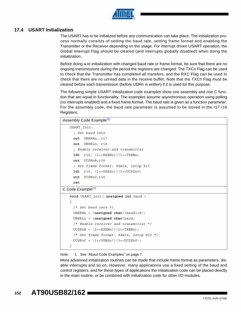
17.4 USART InitializationThe USART has to be initialized before any communication can take place. The initialization pro-cess normally consists of setting the baud rate, setting frame format and enabling the Transmitter or the Receiver depending on the usage. For interrupt driven USART operation, the Global Interrupt Flag should be cleared (and interrupts globally disabled) when doing the initialization.
Before doing a re-initialization with changed baud rate or frame format, be sure that there are no ongoing transmissions during the period the registers are changed. The TXCn Flag can be used to check that the Transmitter has completed all transfers, and the RXC Flag can be used to check that there are no unread data in the receive buffer. Note that the TXCn Flag must be cleared before each transmission (before UDRn is written) if it is used for this purpose.
The following simple USART initialization code examples show one assembly and one C func-tion that are equal in functionality. The examples assume asynchronous operation using polling (no interrupts enabled) and a fixed frame format. The baud rate is given as a function parameter. For the assembly code, the baud rate parameter is assumed to be stored in the r17:r16 Registers.
Note: 1. See “About Code Examples” on page 7.
More advanced initialization routines can be made that include frame format as parameters, dis-able interrupts and so on. However, many applications use a fixed setting of the baud and control registers, and for these types of applications the initialization code can be placed directly in the main routine, or be combined with initialization code for other I/O modules.
Assembly Code Example(1)
USART_Init:
; Set baud rate
out UBRRHn, r17
out UBRRLn, r16
; Enable receiver and transmitter
ldi r16, (1<<RXENn)|(1<<TXENn)
out UCSRnB,r16
; Set frame format: 8data, 2stop bit
ldi r16, (1<<USBSn)|(3<<UCSZn0)
out UCSRnC,r16
ret
C Code Example(1)
void USART_Init( unsigned int baud )
{
/* Set baud rate */
UBRRHn = (unsigned char)(baud>>8);
UBRRLn = (unsigned char)baud;
/* Enable receiver and transmitter */
UCSRnB = (1<<RXENn)|(1<<TXENn);
/* Set frame format: 8data, 2stop bit */
UCSRnC = (1<<USBSn)|(3<<UCSZn0);
}
1527707D–AVR–07/08
AT90USB82/162

AT90USB82/162
17.5 Data Transmission – The USART TransmitterThe USART Transmitter is enabled by setting the Transmit Enable (TXEN) bit in the UCSRnB Register. When the Transmitter is enabled, the normal port operation of the TxDn pin is overrid-den by the USART and given the function as the Transmitter’s serial output. The baud rate, mode of operation and frame format must be set up once before doing any transmissions. If syn-chronous operation is used, the clock on the XCKn pin will be overridden and used as transmission clock.
17.5.1 Sending Frames with 5 to 8 Data BitA data transmission is initiated by loading the transmit buffer with the data to be transmitted. The CPU can load the transmit buffer by writing to the UDRn I/O location. The buffered data in the transmit buffer will be moved to the Shift Register when the Shift Register is ready to send a new frame. The Shift Register is loaded with new data if it is in idle state (no ongoing transmission) or immediately after the last stop bit of the previous frame is transmitted. When the Shift Register is loaded with new data, it will transfer one complete frame at the rate given by the Baud Register, U2Xn bit or by XCKn depending on mode of operation.
The following code examples show a simple USART transmit function based on polling of the Data Register Empty (UDREn) Flag. When using frames with less than eight bits, the most sig-nificant bits written to the UDRn are ignored. The USART has to be initialized before the function can be used. For the assembly code, the data to be sent is assumed to be stored in Register R16
Note: 1. See “About Code Examples” on page 7.
The function simply waits for the transmit buffer to be empty by checking the UDREn Flag, before loading it with new data to be transmitted. If the Data Register Empty interrupt is utilized, the interrupt routine writes the data into the buffer.
17.5.2 Sending Frames with 9 Data BitIf 9-bit characters are used (UCSZn = 7), the ninth bit must be written to the TXB8 bit in UCS-RnB before the low byte of the character is written to UDRn. The following code examples show
Assembly Code Example(1)
USART_Transmit:
; Wait for empty transmit buffer
sbis UCSRnA,UDREn
rjmp USART_Transmit
; Put data (r16) into buffer, sends the data
out UDRn,r16
ret
C Code Example(1)
void USART_Transmit( unsigned char data )
{
/* Wait for empty transmit buffer */
while ( !( UCSRnA & (1<<UDREn)) )
;
/* Put data into buffer, sends the data */
UDRn = data;
}
1537707D–AVR–07/08
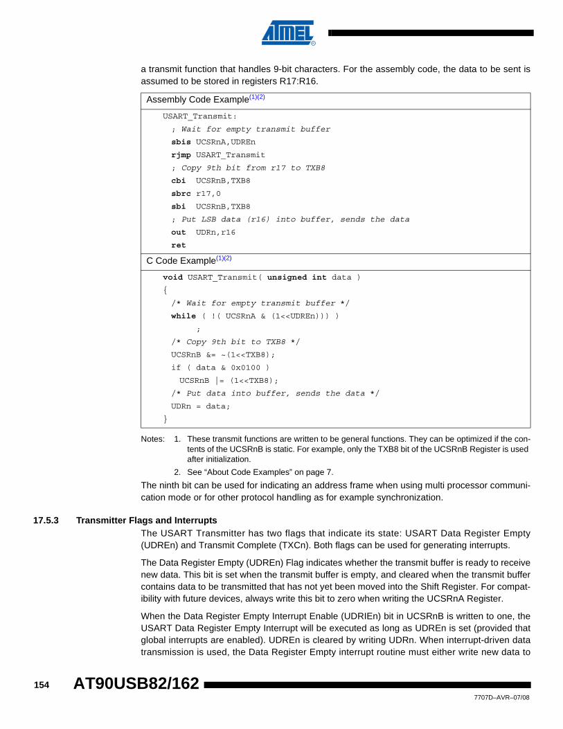
a transmit function that handles 9-bit characters. For the assembly code, the data to be sent is assumed to be stored in registers R17:R16.
Notes: 1. These transmit functions are written to be general functions. They can be optimized if the con-tents of the UCSRnB is static. For example, only the TXB8 bit of the UCSRnB Register is used after initialization.
2. See “About Code Examples” on page 7.
The ninth bit can be used for indicating an address frame when using multi processor communi-cation mode or for other protocol handling as for example synchronization.
17.5.3 Transmitter Flags and InterruptsThe USART Transmitter has two flags that indicate its state: USART Data Register Empty (UDREn) and Transmit Complete (TXCn). Both flags can be used for generating interrupts.
The Data Register Empty (UDREn) Flag indicates whether the transmit buffer is ready to receive new data. This bit is set when the transmit buffer is empty, and cleared when the transmit buffer contains data to be transmitted that has not yet been moved into the Shift Register. For compat-ibility with future devices, always write this bit to zero when writing the UCSRnA Register.
When the Data Register Empty Interrupt Enable (UDRIEn) bit in UCSRnB is written to one, the USART Data Register Empty Interrupt will be executed as long as UDREn is set (provided that global interrupts are enabled). UDREn is cleared by writing UDRn. When interrupt-driven data transmission is used, the Data Register Empty interrupt routine must either write new data to
Assembly Code Example(1)(2)
USART_Transmit:
; Wait for empty transmit buffer
sbis UCSRnA,UDREn
rjmp USART_Transmit
; Copy 9th bit from r17 to TXB8
cbi UCSRnB,TXB8
sbrc r17,0
sbi UCSRnB,TXB8
; Put LSB data (r16) into buffer, sends the data
out UDRn,r16
ret
C Code Example(1)(2)
void USART_Transmit( unsigned int data )
{
/* Wait for empty transmit buffer */
while ( !( UCSRnA & (1<<UDREn))) )
;
/* Copy 9th bit to TXB8 */
UCSRnB &= ~(1<<TXB8);
if ( data & 0x0100 )
UCSRnB |= (1<<TXB8);
/* Put data into buffer, sends the data */
UDRn = data;
}
1547707D–AVR–07/08
AT90USB82/162

AT90USB82/162
UDRn in order to clear UDREn or disable the Data Register Empty interrupt, otherwise a new interrupt will occur once the interrupt routine terminates.
The Transmit Complete (TXCn) Flag bit is set one when the entire frame in the Transmit Shift Register has been shifted out and there are no new data currently present in the transmit buffer. The TXCn Flag bit is automatically cleared when a transmit complete interrupt is executed, or it can be cleared by writing a one to its bit location. The TXCn Flag is useful in half-duplex commu-nication interfaces (like the RS-485 standard), where a transmitting application must enter receive mode and free the communication bus immediately after completing the transmission.
When the Transmit Compete Interrupt Enable (TXCIEn) bit in UCSRnB is set, the USART Transmit Complete Interrupt will be executed when the TXCn Flag becomes set (provided that global interrupts are enabled). When the transmit complete interrupt is used, the interrupt han-dling routine does not have to clear the TXCn Flag, this is done automatically when the interrupt is executed.
17.5.4 Parity GeneratorThe Parity Generator calculates the parity bit for the serial frame data. When parity bit is enabled (UPMn1 = 1), the transmitter control logic inserts the parity bit between the last data bit and the first stop bit of the frame that is sent.
17.5.5 Disabling the TransmitterThe disabling of the Transmitter (setting the TXEN to zero) will not become effective until ongo-ing and pending transmissions are completed, i.e., when the Transmit Shift Register and Transmit Buffer Register do not contain data to be transmitted. When disabled, the Transmitter will no longer override the TxDn pin.
17.6 Data Reception – The USART ReceiverThe USART Receiver is enabled by writing the Receive Enable (RXENn) bit in the UCSRnB Register to one. When the Receiver is enabled, the normal pin operation of the RxDn pin is overridden by the USART and given the function as the Receiver’s serial input. The baud rate, mode of operation and frame format must be set up once before any serial reception can be done. If synchronous operation is used, the clock on the XCKn pin will be used as transfer clock.
17.6.1 Receiving Frames with 5 to 8 Data BitsThe Receiver starts data reception when it detects a valid start bit. Each bit that follows the start bit will be sampled at the baud rate or XCKn clock, and shifted into the Receive Shift Register until the first stop bit of a frame is received. A second stop bit will be ignored by the Receiver. When the first stop bit is received, i.e., a complete serial frame is present in the Receive Shift Register, the contents of the Shift Register will be moved into the receive buffer. The receive buffer can then be read by reading the UDRn I/O location.
The following code example shows a simple USART receive function based on polling of the Receive Complete (RXCn) Flag. When using frames with less than eight bits the most significant
1557707D–AVR–07/08

bits of the data read from the UDRn will be masked to zero. The USART has to be initialized before the function can be used.
Note: 1. See “About Code Examples” on page 7.
The function simply waits for data to be present in the receive buffer by checking the RXCn Flag, before reading the buffer and returning the value.
17.6.2 Receiving Frames with 9 Data BitsIf 9-bit characters are used (UCSZn=7) the ninth bit must be read from the RXB8n bit in UCS-RnB before reading the low bits from the UDRn. This rule applies to the FEn, DORn and UPEn Status Flags as well. Read status from UCSRnA, then data from UDRn. Reading the UDRn I/O location will change the state of the receive buffer FIFO and consequently the TXB8n, FEn, DORn and UPEn bits, which all are stored in the FIFO, will change.
The following code example shows a simple USART receive function that handles both nine bit characters and the status bits.
Assembly Code Example(1)
USART_Receive:
; Wait for data to be received
sbis UCSRnA, RXCn
rjmp USART_Receive
; Get and return received data from buffer
in r16, UDRn
ret
C Code Example(1)
unsigned char USART_Receive( void )
{
/* Wait for data to be received */
while ( !(UCSRnA & (1<<RXCn)) )
;
/* Get and return received data from buffer */
return UDRn;
}
1567707D–AVR–07/08
AT90USB82/162

AT90USB82/162
Note: 1. See “About Code Examples” on page 7.
The receive function example reads all the I/O Registers into the Register File before any com-putation is done. This gives an optimal receive buffer utilization since the buffer location read will be free to accept new data as early as possible.
Assembly Code Example(1)
USART_Receive:
; Wait for data to be received
sbis UCSRnA, RXCn
rjmp USART_Receive
; Get status and 9th bit, then data from buffer
in r18, UCSRnA
in r17, UCSRnB
in r16, UDRn
; If error, return -1
andi r18,(1<<FEn)|(1<<DORn)|(1<<UPEn)
breq USART_ReceiveNoError
ldi r17, HIGH(-1)
ldi r16, LOW(-1)
USART_ReceiveNoError:
; Filter the 9th bit, then return
lsr r17
andi r17, 0x01
ret
C Code Example(1)
unsigned int USART_Receive( void )
{
unsigned char status, resh, resl;
/* Wait for data to be received */
while ( !(UCSRnA & (1<<RXCn)) )
;
/* Get status and 9th bit, then data */
/* from buffer */
status = UCSRnA;
resh = UCSRnB;
resl = UDRn;
/* If error, return -1 */
if ( status & (1<<FEn)|(1<<DORn)|(1<<UPEn) )
return -1;
/* Filter the 9th bit, then return */
resh = (resh >> 1) & 0x01;
return ((resh << 8) | resl);
}
1577707D–AVR–07/08

17.6.3 Receive Compete Flag and InterruptThe USART Receiver has one flag that indicates the Receiver state.
The Receive Complete (RXCn) Flag indicates if there are unread data present in the receive buffer. This flag is one when unread data exist in the receive buffer, and zero when the receive buffer is empty (i.e., does not contain any unread data). If the Receiver is disabled (RXENn = 0), the receive buffer will be flushed and consequently the RXCn bit will become zero.
When the Receive Complete Interrupt Enable (RXCIEn) in UCSRnB is set, the USART Receive Complete interrupt will be executed as long as the RXCn Flag is set (provided that global inter-rupts are enabled). When interrupt-driven data reception is used, the receive complete routine must read the received data from UDRn in order to clear the RXCn Flag, otherwise a new inter-rupt will occur once the interrupt routine terminates.
17.6.4 Receiver Error FlagsThe USART Receiver has three Error Flags: Frame Error (FEn), Data OverRun (DORn) and Parity Error (UPEn). All can be accessed by reading UCSRnA. Common for the Error Flags is that they are located in the receive buffer together with the frame for which they indicate the error status. Due to the buffering of the Error Flags, the UCSRnA must be read before the receive buffer (UDRn), since reading the UDRn I/O location changes the buffer read location. Another equality for the Error Flags is that they can not be altered by software doing a write to the flag location. However, all flags must be set to zero when the UCSRnA is written for upward compatibility of future USART implementations. None of the Error Flags can generate interrupts.
The Frame Error (FEn) Flag indicates the state of the first stop bit of the next readable frame stored in the receive buffer. The FEn Flag is zero when the stop bit was correctly read (as one), and the FEn Flag will be one when the stop bit was incorrect (zero). This flag can be used for detecting out-of-sync conditions, detecting break conditions and protocol handling. The FEn Flag is not affected by the setting of the USBSn bit in UCSRnC since the Receiver ignores all, except for the first, stop bits. For compatibility with future devices, always set this bit to zero when writing to UCSRnA.
The Data OverRun (DORn) Flag indicates data loss due to a receiver buffer full condition. A Data OverRun occurs when the receive buffer is full (two characters), it is a new character wait-ing in the Receive Shift Register, and a new start bit is detected. If the DORn Flag is set there was one or more serial frame lost between the frame last read from UDRn, and the next frame read from UDRn. For compatibility with future devices, always write this bit to zero when writing to UCSRnA. The DORn Flag is cleared when the frame received was successfully moved from the Shift Register to the receive buffer.
The Parity Error (UPEn) Flag indicates that the next frame in the receive buffer had a Parity Error when received. If Parity Check is not enabled the UPEn bit will always be read zero. For compatibility with future devices, always set this bit to zero when writing to UCSRnA. For more details see “Parity Bit Calculation” on page 151 and “Parity Checker” on page 158.
17.6.5 Parity CheckerThe Parity Checker is active when the high USART Parity mode (UPMn1) bit is set. Type of Par-ity Check to be performed (odd or even) is selected by the UPMn0 bit. When enabled, the Parity Checker calculates the parity of the data bits in incoming frames and compares the result with the parity bit from the serial frame. The result of the check is stored in the receive buffer together with the received data and stop bits. The Parity Error (UPEn) Flag can then be read by software to check if the frame had a Parity Error.
1587707D–AVR–07/08
AT90USB82/162

AT90USB82/162
The UPEn bit is set if the next character that can be read from the receive buffer had a Parity Error when received and the Parity Checking was enabled at that point (UPMn1 = 1). This bit is valid until the receive buffer (UDRn) is read.
17.6.6 Disabling the ReceiverIn contrast to the Transmitter, disabling of the Receiver will be immediate. Data from ongoing receptions will therefore be lost. When disabled (i.e., the RXENn is set to zero) the Receiver will no longer override the normal function of the RxDn port pin. The Receiver buffer FIFO will be flushed when the Receiver is disabled. Remaining data in the buffer will be lost
17.6.7 Flushing the Receive BufferThe receiver buffer FIFO will be flushed when the Receiver is disabled, i.e., the buffer will be emptied of its contents. Unread data will be lost. If the buffer has to be flushed during normal operation, due to for instance an error condition, read the UDRn I/O location until the RXCn Flag is cleared. The following code example shows how to flush the receive buffer.
Note: 1. See “About Code Examples” on page 7.
17.7 Asynchronous Data ReceptionThe USART includes a clock recovery and a data recovery unit for handling asynchronous data reception. The clock recovery logic is used for synchronizing the internally generated baud rate clock to the incoming asynchronous serial frames at the RxDn pin. The data recovery logic sam-ples and low pass filters each incoming bit, thereby improving the noise immunity of the Receiver. The asynchronous reception operational range depends on the accuracy of the inter-nal baud rate clock, the rate of the incoming frames, and the frame size in number of bits.
17.7.1 Asynchronous Clock RecoveryThe clock recovery logic synchronizes internal clock to the incoming serial frames. Figure 17-5illustrates the sampling process of the start bit of an incoming frame. The sample rate is 16 times the baud rate for Normal mode, and eight times the baud rate for Double Speed mode. The hor-izontal arrows illustrate the synchronization variation due to the sampling process. Note the larger time variation when using the Double Speed mode (U2Xn = 1) of operation. Samples denoted zero are samples done when the RxDn line is idle (i.e., no communication activity).
Assembly Code Example(1)
USART_Flush:
sbis UCSRnA, RXCn
ret
in r16, UDRn
rjmp USART_Flush
C Code Example(1)
void USART_Flush( void )
{
unsigned char dummy;
while ( UCSRnA & (1<<RXCn) ) dummy = UDRn;
}
1597707D–AVR–07/08

Figure 17-5. Start Bit Sampling
When the clock recovery logic detects a high (idle) to low (start) transition on the RxDn line, the start bit detection sequence is initiated. Let sample 1 denote the first zero-sample as shown in the figure. The clock recovery logic then uses samples 8, 9, and 10 for Normal mode, and sam-ples 4, 5, and 6 for Double Speed mode (indicated with sample numbers inside boxes on the figure), to decide if a valid start bit is received. If two or more of these three samples have logical high levels (the majority wins), the start bit is rejected as a noise spike and the Receiver starts looking for the next high to low-transition. If however, a valid start bit is detected, the clock recov-ery logic is synchronized and the data recovery can begin. The synchronization process is repeated for each start bit.
17.7.2 Asynchronous Data RecoveryWhen the receiver clock is synchronized to the start bit, the data recovery can begin. The data recovery unit uses a state machine that has 16 states for each bit in Normal mode and eight states for each bit in Double Speed mode. Figure 17-6 shows the sampling of the data bits and the parity bit. Each of the samples is given a number that is equal to the state of the recovery unit.
Figure 17-6. Sampling of Data and Parity Bit
The decision of the logic level of the received bit is taken by doing a majority voting of the logic value to the three samples in the center of the received bit. The center samples are emphasized on the figure by having the sample number inside boxes. The majority voting process is done as follows: If two or all three samples have high levels, the received bit is registered to be a logic 1. If two or all three samples have low levels, the received bit is registered to be a logic 0. This majority voting process acts as a low pass filter for the incoming signal on the RxDn pin. The recovery process is then repeated until a complete frame is received. Including the first stop bit. Note that the Receiver only uses the first stop bit of a frame.
Figure 17-7 shows the sampling of the stop bit and the earliest possible beginning of the start bit of the next frame.
1 2 3 4 5 6 7 8 9 10 11 12 13 14 15 16 1 2
STARTIDLE
00
BIT 0
3
1 2 3 4 5 6 7 8 1 20
RxD
Sample(U2X = 0)
Sample(U2X = 1)
1 2 3 4 5 6 7 8 9 10 11 12 13 14 15 16 1
BIT n
1 2 3 4 5 6 7 8 1
RxD
Sample(U2X = 0)
Sample(U2X = 1)
1607707D–AVR–07/08
AT90USB82/162

AT90USB82/162
Figure 17-7. Stop Bit Sampling and Next Start Bit Sampling
The same majority voting is done to the stop bit as done for the other bits in the frame. If the stop bit is registered to have a logic 0 value, the Frame Error (FEn) Flag will be set.
A new high to low transition indicating the start bit of a new frame can come right after the last of the bits used for majority voting. For Normal Speed mode, the first low level sample can be at point marked (A) in Figure 17-7. For Double Speed mode the first low level must be delayed to (B). (C) marks a stop bit of full length. The early start bit detection influences the operational range of the Receiver.
17.7.3 Asynchronous Operational RangeThe operational range of the Receiver is dependent on the mismatch between the received bit rate and the internally generated baud rate. If the Transmitter is sending frames at too fast or too slow bit rates, or the internally generated baud rate of the Receiver does not have a similar (see Table 17-2) base frequency, the Receiver will not be able to synchronize the frames to the start bit.
The following equations can be used to calculate the ratio of the incoming data rate and internal receiver baud rate.
D Sum of character size and parity size (D = 5 to 10 bit)
S Samples per bit. S = 16 for Normal Speed mode and S = 8 for Double Speed mode.
SF First sample number used for majority voting. SF = 8 for normal speed and SF = 4 for Double Speed mode.
SM Middle sample number used for majority voting. SM = 9 for normal speed and SM = 5 for Double Speed mode.
Rslow is the ratio of the slowest incoming data rate that can be accepted in relation to the receiver baud rate. Rfast is the ratio of the fastest incoming data rate that can be accepted in relation to the receiver baud rate.
Table 17-2 and Table 17-3 list the maximum receiver baud rate error that can be tolerated. Note that Normal Speed mode has higher toleration of baud rate variations.
1 2 3 4 5 6 7 8 9 10 0/1 0/1 0/1
STOP 1
1 2 3 4 5 6 0/1
RxD
Sample(U2X = 0)
Sample(U2X = 1)
(A) (B) (C)
RslowD 1+( )S
S 1– D S⋅ SF+ +-------------------------------------------= Rfast
D 2+( )SD 1+( )S SM+
-----------------------------------=
1617707D–AVR–07/08

The recommendations of the maximum receiver baud rate error was made under the assump-tion that the Receiver and Transmitter equally divides the maximum total error.
There are two possible sources for the receivers baud rate error. The Receiver’s system clock (XTAL) will always have some minor instability over the supply voltage range and the tempera-ture range. When using a crystal to generate the system clock, this is rarely a problem, but for a resonator the system clock may differ more than 2% depending of the resonators tolerance. The second source for the error is more controllable. The baud rate generator can not always do an exact division of the system frequency to get the baud rate wanted. In this case an UBRR value that gives an acceptable low error can be used if possible.
17.8 Multi-processor Communication ModeSetting the Multi-processor Communication mode (MPCMn) bit in UCSRnA enables a filtering function of incoming frames received by the USART Receiver. Frames that do not contain address information will be ignored and not put into the receive buffer. This effectively reduces the number of incoming frames that has to be handled by the CPU, in a system with multiple MCUs that communicate via the same serial bus. The Transmitter is unaffected by the MPCMn setting, but has to be used differently when it is a part of a system utilizing the Multi-processor Communication mode.
If the Receiver is set up to receive frames that contain 5 to 8 data bits, then the first stop bit indi-cates if the frame contains data or address information. If the Receiver is set up for frames with nine data bits, then the ninth bit (RXB8n) is used for identifying address and data frames. When the frame type bit (the first stop or the ninth bit) is one, the frame contains an address. When the frame type bit is zero the frame is a data frame.
Table 17-2. Recommended Maximum Receiver Baud Rate Error for Normal Speed Mode (U2Xn = 0)
D# (Data+Parity Bit) Rslow (%) Rfast (%) Max Total Error (%)
Recommended Max Receiver Error (%)
5 93.20 106.67 +6.67/-6.8 ± 3.0
6 94.12 105.79 +5.79/-5.88 ± 2.5
7 94.81 105.11 +5.11/-5.19 ± 2.0
8 95.36 104.58 +4.58/-4.54 ± 2.0
9 95.81 104.14 +4.14/-4.19 ± 1.5
10 96.17 103.78 +3.78/-3.83 ± 1.5
Table 17-3. Recommended Maximum Receiver Baud Rate Error for Double Speed Mode (U2Xn = 1)
D# (Data+Parity Bit) Rslow (%) Rfast (%) Max Total Error (%)
Recommended Max Receiver Error (%)
5 94.12 105.66 +5.66/-5.88 ± 2.5
6 94.92 104.92 +4.92/-5.08 ± 2.0
7 95.52 104,35 +4.35/-4.48 ± 1.5
8 96.00 103.90 +3.90/-4.00 ± 1.5
9 96.39 103.53 +3.53/-3.61 ± 1.5
10 96.70 103.23 +3.23/-3.30 ± 1.0
1627707D–AVR–07/08
AT90USB82/162

AT90USB82/162
The Multi-processor Communication mode enables several slave MCUs to receive data from a master MCU. This is done by first decoding an address frame to find out which MCU has been addressed. If a particular slave MCU has been addressed, it will receive the following data frames as normal, while the other slave MCUs will ignore the received frames until another address frame is received.
17.8.1 Using MPCMnFor an MCU to act as a master MCU, it can use a 9-bit character frame format (UCSZn = 7). The ninth bit (TXB8n) must be set when an address frame (TXB8n = 1) or cleared when a data frame (TXB = 0) is being transmitted. The slave MCUs must in this case be set to use a 9-bit character frame format.
The following procedure should be used to exchange data in Multi-processor Communication mode:
1. All Slave MCUs are in Multi-processor Communication mode (MPCMn in UCSRnA is set).
2. The Master MCU sends an address frame, and all slaves receive and read this frame. In the Slave MCUs, the RXCn Flag in UCSRnA will be set as normal.
3. Each Slave MCU reads the UDRn Register and determines if it has been selected. If so, it clears the MPCMn bit in UCSRnA, otherwise it waits for the next address byte and keeps the MPCMn setting.
4. The addressed MCU will receive all data frames until a new address frame is received. The other Slave MCUs, which still have the MPCMn bit set, will ignore the data frames.
5. When the last data frame is received by the addressed MCU, the addressed MCU sets the MPCMn bit and waits for a new address frame from master. The process then repeats from 2.
Using any of the 5- to 8-bit character frame formats is possible, but impractical since the Receiver must change between using n and n+1 character frame formats. This makes full-duplex operation difficult since the Transmitter and Receiver uses the same character size set-ting. If 5- to 8-bit character frames are used, the Transmitter must be set to use two stop bit (USBSn = 1) since the first stop bit is used for indicating the frame type.
Do not use Read-Modify-Write instructions (SBI and CBI) to set or clear the MPCMn bit. The MPCMn bit shares the same I/O location as the TXCn Flag and this might accidentally be cleared when using SBI or CBI instructions.
17.9 Hardware Flow ControlThe hardware flow control can be enabled by software.CTS : (Clear to Send) RTS : (Request to Send)
17.9.1 Receiver Flow ControlThe reception flow can be controlled by hardware using the RTS pin. The aim of the flow control is to inform the external transmitter when the internal receive Fifo is full. Thus the transmitter can
TXDAT90USB82/162
RTS
TXD
RXD
HOST
RXD
CTSCTS
RTS
1637707D–AVR–07/08
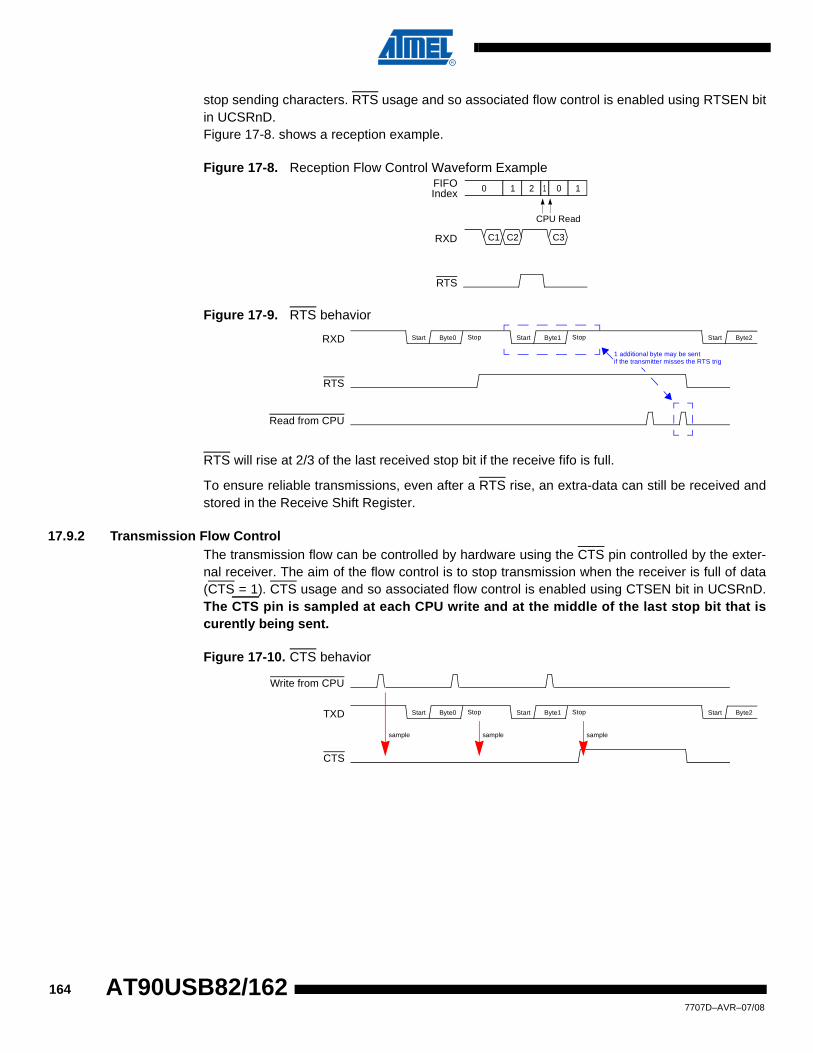
stop sending characters. RTS usage and so associated flow control is enabled using RTSEN bit in UCSRnD. Figure 17-8. shows a reception example.
Figure 17-8. Reception Flow Control Waveform Example
Figure 17-9. RTS behavior
RTS will rise at 2/3 of the last received stop bit if the receive fifo is full.
To ensure reliable transmissions, even after a RTS rise, an extra-data can still be received and stored in the Receive Shift Register.
17.9.2 Transmission Flow ControlThe transmission flow can be controlled by hardware using the CTS pin controlled by the exter-nal receiver. The aim of the flow control is to stop transmission when the receiver is full of data (CTS = 1). CTS usage and so associated flow control is enabled using CTSEN bit in UCSRnD. The CTS pin is sampled at each CPU write and at the middle of the last stop bit that is curently being sent.
Figure 17-10. CTS behavior
RTS
RXD C1 C2
0 1 2FIFO 1
CPU Read
Index
C3
10
RTS
RXD Start Byte0 Stop Start Byte1 Stop
Read from CPU
Start Byte2
1 additional byte may be sentif the transmitter misses the RTS trig
CTS
TXD Start Byte0 Stop Start Byte1 Stop Start Byte2
sample sample
Write from CPU
sample
1647707D–AVR–07/08
AT90USB82/162

AT90USB82/162
17.10 USART Register Description
17.10.1 USART I/O Data Register n– UDRn
The USART Transmit Data Buffer Register and USART Receive Data Buffer Registers share the same I/O address referred to as USART Data Register or UDRn. The Transmit Data Buffer Reg-ister (TXB) will be the destination for data written to the UDRn Register location. Reading the UDRn Register location will return the contents of the Receive Data Buffer Register (RXB).
For 5-, 6-, or 7-bit characters the upper unused bits will be ignored by the Transmitter and set to zero by the Receiver.
The transmit buffer can only be written when the UDREn Flag in the UCSRnA Register is set. Data written to UDRn when the UDREn Flag is not set, will be ignored by the USART Transmit-ter. When data is written to the transmit buffer, and the Transmitter is enabled, the Transmitter will load the data into the Transmit Shift Register when the Shift Register is empty. Then the data will be serially transmitted on the TxDn pin.
The receive buffer consists of a two level FIFO. The FIFO will change its state whenever the receive buffer is accessed. Due to this behavior of the receive buffer, do not use Read-Modify-Write instructions (SBI and CBI) on this location. Be careful when using bit test instructions (SBIC and SBIS), since these also will change the state of the FIFO.
17.10.2 USART Control and Status Register A – UCSRnA
• Bit 7 – RXCn: USART Receive CompleteThis flag bit is set when there are unread data in the receive buffer and cleared when the receive buffer is empty (i.e., does not contain any unread data). If the Receiver is disabled, the receive buffer will be flushed and consequently the RXCn bit will become zero. The RXCn Flag can be used to generate a Receive Complete interrupt (see description of the RXCIEn bit).
• Bit 6 – TXCn: USART Transmit CompleteThis flag bit is set when the entire frame in the Transmit Shift Register has been shifted out and there are no new data currently present in the transmit buffer (UDRn). The TXCn Flag bit is auto-matically cleared when a transmit complete interrupt is executed, or it can be cleared by writing a one to its bit location. The TXCn Flag can generate a Transmit Complete interrupt (see description of the TXCIEn bit).
• Bit 5 – UDREn: USART Data Register EmptyThe UDREn Flag indicates if the transmit buffer (UDRn) is ready to receive new data. If UDREn is one, the buffer is empty, and therefore ready to be written. The UDREn Flag can generate a Data Register Empty interrupt (see description of the UDRIEn bit).
UDREn is set after a reset to indicate that the Transmitter is ready.
Bit 7 6 5 4 3 2 1 0
RXB[7:0] UDRn (Read)
TXB[7:0] UDRn (Write)
Read/Write R/W R/W R/W R/W R/W R/W R/W R/W
Initial Value 0 0 0 0 0 0 0 0
Bit 7 6 5 4 3 2 1 0
RXCn TXCn UDREn FEn DORn UPEn U2Xn MPCMn UCSRnA
Read/Write R R/W R R R R R/W R/W
Initial Value 0 0 1 0 0 0 0 0
1657707D–AVR–07/08

• Bit 4 – FEn: Frame ErrorThis bit is set if the next character in the receive buffer had a Frame Error when received. I.e., when the first stop bit of the next character in the receive buffer is zero. This bit is valid until the receive buffer (UDRn) is read. The FEn bit is zero when the stop bit of received data is one. Always set this bit to zero when writing to UCSRnA.
• Bit 3 – DORn: Data OverRunThis bit is set if a Data OverRun condition is detected. A Data OverRun occurs when the receive buffer is full (two characters), it is a new character waiting in the Receive Shift Register, and a new start bit is detected. This bit is valid until the receive buffer (UDRn) is read. Always set this bit to zero when writing to UCSRnA.
• Bit 2 – UPEn: USART Parity ErrorThis bit is set if the next character in the receive buffer had a Parity Error when received and the Parity Checking was enabled at that point (UPMn1 = 1). This bit is valid until the receive buffer (UDRn) is read. Always set this bit to zero when writing to UCSRnA.
• Bit 1 – U2Xn: Double the USART Transmission SpeedThis bit only has effect for the asynchronous operation. Write this bit to zero when using syn-chronous operation.
Writing this bit to one will reduce the divisor of the baud rate divider from 16 to 8 effectively dou-bling the transfer rate for asynchronous communication.
• Bit 0 – MPCMn: Multi-processor Communication ModeThis bit enables the Multi-processor Communication mode. When the MPCMn bit is written to one, all the incoming frames received by the USART Receiver that do not contain address infor-mation will be ignored. The Transmitter is unaffected by the MPCMn setting. For more detailed information see “Multi-processor Communication Mode” on page 162.
17.10.3 USART Control and Status Register n B – UCSRnB
• Bit 7 – RXCIEn: RX Complete Interrupt Enable nWriting this bit to one enables interrupt on the RXCn Flag. A USART Receive Complete interrupt will be generated only if the RXCIEn bit is written to one, the Global Interrupt Flag in SREG is written to one and the RXCn bit in UCSRnA is set.
• Bit 6 – TXCIEn: TX Complete Interrupt Enable nWriting this bit to one enables interrupt on the TXCn Flag. A USART Transmit Complete interrupt will be generated only if the TXCIEn bit is written to one, the Global Interrupt Flag in SREG is written to one and the TXCn bit in UCSRnA is set.
• Bit 5 – UDRIEn: USART Data Register Empty Interrupt Enable nWriting this bit to one enables interrupt on the UDREn Flag. A Data Register Empty interrupt will be generated only if the UDRIEn bit is written to one, the Global Interrupt Flag in SREG is written to one and the UDREn bit in UCSRnA is set.
Bit 7 6 5 4 3 2 1 0
RXCIEn TXCIEn UDRIEn RXENn TXENn UCSZn2 RXB8n TXB8n UCSRnB
Read/Write R/W R/W R/W R/W R/W R/W R R/W
Initial Value 0 0 0 0 0 0 0 0
1667707D–AVR–07/08
AT90USB82/162

AT90USB82/162
• Bit 4 – RXENn: Receiver Enable nWriting this bit to one enables the USART Receiver. The Receiver will override normal port oper-ation for the RxDn pin when enabled. Disabling the Receiver will flush the receive buffer invalidating the FEn, DORn, and UPEn Flags.
• Bit 3 – TXENn: Transmitter Enable nWriting this bit to one enables the USART Transmitter. The Transmitter will override normal port operation for the TxDn pin when enabled. The disabling of the Transmitter (writing TXENn to zero) will not become effective until ongoing and pending transmissions are completed, i.e., when the Transmit Shift Register and Transmit Buffer Register do not contain data to be trans-mitted. When disabled, the Transmitter will no longer override the TxDn port.
• Bit 2 – UCSZn2: Character Size nThe UCSZn2 bits combined with the UCSZn1:0 bit in UCSRnC sets the number of data bits (Character SiZe) in a frame the Receiver and Transmitter use.
• Bit 1 – RXB8n: Receive Data Bit 8 nRXB8n is the ninth data bit of the received character when operating with serial frames with nine data bits. Must be read before reading the low bits from UDRn.
• Bit 0 – TXB8n: Transmit Data Bit 8 nTXB8n is the ninth data bit in the character to be transmitted when operating with serial frames with nine data bits. Must be written before writing the low bits to UDRn.
17.10.4 USART Control and Status Register n C – UCSRnC
• Bits 7:6 – UMSELn1:0 USART Mode SelectThese bits select the mode of operation of the USARTn as shown in Table 17-4..
Note: 1. See “USART in SPI Mode” on page 173 for full description of the Master SPI Mode (MSPIM) operation
• Bits 5:4 – UPMn1:0: Parity ModeThese bits enable and set type of parity generation and check. If enabled, the Transmitter will automatically generate and send the parity of the transmitted data bits within each frame. The
Bit 7 6 5 4 3 2 1 0
UMSELn1 UMSELn0 UPMn1 UPMn0 USBSn UCSZn1 UCSZn0 UCPOLn UCSRnC
Read/Write R/W R/W R/W R/W R/W R/W R/W R/W
Initial Value 0 0 0 0 0 1 1 0
Table 17-4. UMSELn Bits Settings
UMSELn1 UMSELn0 Mode
0 0 Asynchronous USART
0 1 Synchronous USART
1 0 (Reserved)
1 1 Master SPI (MSPIM)(1)
1677707D–AVR–07/08

Receiver will generate a parity value for the incoming data and compare it to the UPMn setting. If a mismatch is detected, the UPEn Flag in UCSRnA will be set.
• Bit 3 – USBSn: Stop Bit SelectThis bit selects the number of stop bits to be inserted by the Transmitter. The Receiver ignores this setting.
• Bit 2:1 – UCSZn1:0: Character SizeThe UCSZn1:0 bits combined with the UCSZn2 bit in UCSRnB sets the number of data bits (Character SiZe) in a frame the Receiver and Transmitter use.
• Bit 0 – UCPOLn: Clock PolarityThis bit is used for synchronous mode only. Write this bit to zero when asynchronous mode is used. The UCPOLn bit sets the relationship between data output change and data input sample, and the synchronous clock (XCKn).
Table 17-5. UPMn Bits Settings
UPMn1 UPMn0 Parity Mode
0 0 Disabled
0 1 Reserved
1 0 Enabled, Even Parity
1 1 Enabled, Odd Parity
Table 17-6. USBS Bit Settings
USBSn Stop Bit(s)
0 1-bit
1 2-bit
Table 17-7. UCSZn Bits Settings
UCSZn2 UCSZn1 UCSZn0 Character Size
0 0 0 5-bit
0 0 1 6-bit
0 1 0 7-bit
0 1 1 8-bit
1 0 0 Reserved
1 0 1 Reserved
1 1 0 Reserved
1 1 1 9-bit
Table 17-8. UCPOLn Bit Settings
UCPOLn Transmitted Data Changed (Output of TxDn Pin) Received Data Sampled (Input on RxDn Pin)
0 Rising XCKn Edge Falling XCKn Edge
1 Falling XCKn Edge Rising XCKn Edge
1687707D–AVR–07/08
AT90USB82/162

AT90USB82/162
17.10.5 USART Control and Status Register n D – UCSRnD
• Bits 1 – CTSEN : USART CTS EnableSet this bit to one by firmware to enable the transmission flow control (CTS). Transmission is allowed if CTS = 0. Set this bit to zero by firmware to disable the transmission flow control (CTS). Transmission is always allowed.
• Bits 0 – RTSEN : USART RTS EnableSet this bit to one by firmware to enable the receive flow control (RTS). Set this bit to zero by firmware to disable the receive flow control (RTS).
17.10.6 USART Baud Rate Registers – UBRRLn and UBRRHn
• Bit 15:12 – Reserved BitsThese bits are reserved for future use. For compatibility with future devices, these bit must be written to zero when UBRRH is written.
• Bit 11:0 – UBRR11:0: USART Baud Rate RegisterThis is a 12-bit register which contains the USART baud rate. The UBRRH contains the four most significant bits, and the UBRRL contains the eight least significant bits of the USART baud rate. Ongoing transmissions by the Transmitter and Receiver will be corrupted if the baud rate is changed. Writing UBRRL will trigger an immediate update of the baud rate prescaler.
17.11 Examples of Baud Rate SettingFor standard crystal and resonator frequencies, the most commonly used baud rates for asyn-chronous operation can be generated by using the UBRR settings in Table 17-9 to Table 17-12. UBRR values which yield an actual baud rate differing less than 0.5% from the target baud rate, are bold in the table. Higher error ratings are acceptable, but the Receiver will have less noise resistance when the error ratings are high, especially for large serial frames (see “Asynchronous Operational Range” on page 161). The error values are calculated using the following equation:
Bit 7 6 5 4 3 2 1 0
- - - - - - CTSEN RTSEN UCSRnD
Read/Write R/W R/W R/W R/W R/W R/W R/W R/W
Initial Value 0 0 0 0 0 0 0 0
Bit 15 14 13 12 11 10 9 8
– – – – UBRR[11:8] UBRRHn
UBRR[7:0] UBRRLn
7 6 5 4 3 2 1 0
Read/Write R R R R R/W R/W R/W R/W
R/W R/W R/W R/W R/W R/W R/W R/W
Initial Value 0 0 0 0 0 0 0 0
0 0 0 0 0 0 0 0
Error[%]BaudRateClosest Match
BaudRate-------------------------------------------------------- 1–⎝ ⎠⎛ ⎞ 100%•=
1697707D–AVR–07/08

Table 17-9. Examples of UBRRn Settings for Commonly Used Oscillator Frequencies
Baud Rate (bps)
fosc = 1.0000 MHz fosc = 1.8432 MHz fosc = 2.0000 MHz
U2Xn = 0 U2Xn = 1 U2Xn = 0 U2Xn = 1 U2Xn = 0 U2Xn = 1
UBRR Error UBRR Error UBRR Error UBRR Error UBRR Error UBRR Error
2400 25 0.2% 51 0.2% 47 0.0% 95 0.0% 51 0.2% 103 0.2%
4800 12 0.2% 25 0.2% 23 0.0% 47 0.0% 25 0.2% 51 0.2%
9600 6 -7.0% 12 0.2% 11 0.0% 23 0.0% 12 0.2% 25 0.2%
14.4k 3 8.5% 8 -3.5% 7 0.0% 15 0.0% 8 -3.5% 16 2.1%
19.2k 2 8.5% 6 -7.0% 5 0.0% 11 0.0% 6 -7.0% 12 0.2%
28.8k 1 8.5% 3 8.5% 3 0.0% 7 0.0% 3 8.5% 8 -3.5%
38.4k 1 -18.6% 2 8.5% 2 0.0% 5 0.0% 2 8.5% 6 -7.0%
57.6k 0 8.5% 1 8.5% 1 0.0% 3 0.0% 1 8.5% 3 8.5%
76.8k – – 1 -18.6% 1 -25.0% 2 0.0% 1 -18.6% 2 8.5%
115.2k – – 0 8.5% 0 0.0% 1 0.0% 0 8.5% 1 8.5%
230.4k – – – – – – 0 0.0% – – – –
250k – – – – – – – – – – 0 0.0%
Max. (1) 62.5 kbps 125 kbps 115.2 kbps 230.4 kbps 125 kbps 250 kbps
1. UBRR = 0, Error = 0.0%
1707707D–AVR–07/08
AT90USB82/162

AT90USB82/162
Table 17-10. Examples of UBRRn Settings for Commonly Used Oscillator Frequencies (Continued)
Baud Rate (bps)
fosc = 3.6864 MHz fosc = 4.0000 MHz fosc = 7.3728 MHz
U2Xn = 0 U2Xn = 1 U2Xn = 0 U2Xn = 1 U2Xn = 0 U2Xn = 1
UBRR Error UBRR Error UBRR Error UBRR Error UBRR Error UBRR Error
2400 95 0.0% 191 0.0% 103 0.2% 207 0.2% 191 0.0% 383 0.0%
4800 47 0.0% 95 0.0% 51 0.2% 103 0.2% 95 0.0% 191 0.0%
9600 23 0.0% 47 0.0% 25 0.2% 51 0.2% 47 0.0% 95 0.0%
14.4k 15 0.0% 31 0.0% 16 2.1% 34 -0.8% 31 0.0% 63 0.0%
19.2k 11 0.0% 23 0.0% 12 0.2% 25 0.2% 23 0.0% 47 0.0%
28.8k 7 0.0% 15 0.0% 8 -3.5% 16 2.1% 15 0.0% 31 0.0%
38.4k 5 0.0% 11 0.0% 6 -7.0% 12 0.2% 11 0.0% 23 0.0%
57.6k 3 0.0% 7 0.0% 3 8.5% 8 -3.5% 7 0.0% 15 0.0%
76.8k 2 0.0% 5 0.0% 2 8.5% 6 -7.0% 5 0.0% 11 0.0%
115.2k 1 0.0% 3 0.0% 1 8.5% 3 8.5% 3 0.0% 7 0.0%
230.4k 0 0.0% 1 0.0% 0 8.5% 1 8.5% 1 0.0% 3 0.0%
250k 0 -7.8% 1 -7.8% 0 0.0% 1 0.0% 1 -7.8% 3 -7.8%
0.5M – – 0 -7.8% – – 0 0.0% 0 -7.8% 1 -7.8%
1M – – – – – – – – – – 0 -7.8%
Max. (1) 230.4 kbps 460.8 kbps 250 kbps 0.5 Mbps 460.8 kbps 921.6 kbps
1. UBRR = 0, Error = 0.0%
1717707D–AVR–07/08

Table 17-11. Examples of UBRRn Settings for Commonly Used Oscillator Frequencies (Continued)
Baud Rate (bps)
fosc = 8.0000 MHz fosc = 11.0592 MHz fosc = 14.7456 MHz
U2Xn = 0 U2Xn = 1 U2Xn = 0 U2Xn = 1 U2Xn = 0 U2Xn = 1
UBRR Error UBRR Error UBRR Error UBRR Error UBRR Error UBRR Error
2400 207 0.2% 416 -0.1% 287 0.0% 575 0.0% 383 0.0% 767 0.0%
4800 103 0.2% 207 0.2% 143 0.0% 287 0.0% 191 0.0% 383 0.0%
9600 51 0.2% 103 0.2% 71 0.0% 143 0.0% 95 0.0% 191 0.0%
14.4k 34 -0.8% 68 0.6% 47 0.0% 95 0.0% 63 0.0% 127 0.0%
19.2k 25 0.2% 51 0.2% 35 0.0% 71 0.0% 47 0.0% 95 0.0%
28.8k 16 2.1% 34 -0.8% 23 0.0% 47 0.0% 31 0.0% 63 0.0%
38.4k 12 0.2% 25 0.2% 17 0.0% 35 0.0% 23 0.0% 47 0.0%
57.6k 8 -3.5% 16 2.1% 11 0.0% 23 0.0% 15 0.0% 31 0.0%
76.8k 6 -7.0% 12 0.2% 8 0.0% 17 0.0% 11 0.0% 23 0.0%
115.2k 3 8.5% 8 -3.5% 5 0.0% 11 0.0% 7 0.0% 15 0.0%
230.4k 1 8.5% 3 8.5% 2 0.0% 5 0.0% 3 0.0% 7 0.0%
250k 1 0.0% 3 0.0% 2 -7.8% 5 -7.8% 3 -7.8% 6 5.3%
0.5M 0 0.0% 1 0.0% – – 2 -7.8% 1 -7.8% 3 -7.8%
1M – – 0 0.0% – – – – 0 -7.8% 1 -7.8%
Max. (1) 0.5 Mbps 1 Mbps 691.2 kbps 1.3824 Mbps 921.6 kbps 1.8432 Mbps
1. UBRR = 0, Error = 0.0%
1727707D–AVR–07/08
AT90USB82/162

AT90USB82/162
18. USART in SPI ModeThe Universal Synchronous and Asynchronous serial Receiver and Transmitter (USART) can be set to a master SPI compliant mode of operation. The Master SPI Mode (MSPIM) has the follow-ing features:
• Full Duplex, Three-wire Synchronous Data Transfer• Master Operation• Supports all four SPI Modes of Operation (Mode 0, 1, 2, and 3)• LSB First or MSB First Data Transfer (Configurable Data Order)• Queued Operation (Double Buffered)• High Resolution Baud Rate Generator• High Speed Operation (fXCKmax = fCK/2)• Flexible Interrupt Generation
18.1 OverviewSetting both UMSELn1:0 bits to one enables the USART in MSPIM logic. In this mode of opera-tion the SPI master control logic takes direct control over the USART resources. These resources include the transmitter and receiver shift register and buffers, and the baud rate gen-erator. The parity generator and checker, the data and clock recovery logic, and the RX and TX
Table 17-12. Examples of UBRRn Settings for Commonly Used Oscillator Frequencies (Continued)
Baud Rate (bps)
fosc = 16.0000 MHz fosc = 18.4320 MHz fosc = 20.0000 MHz
U2Xn = 0 U2Xn = 1 U2Xn = 0 U2Xn = 1 U2Xn = 0 U2Xn = 1
UBRR Error UBRR Error UBRR Error UBRR Error UBRR Error UBRR Error
2400 416 -0.1% 832 0.0% 479 0.0% 959 0.0% 520 0.0% 1041 0.0%
4800 207 0.2% 416 -0.1% 239 0.0% 479 0.0% 259 0.2% 520 0.0%
9600 103 0.2% 207 0.2% 119 0.0% 239 0.0% 129 0.2% 259 0.2%
14.4k 68 0.6% 138 -0.1% 79 0.0% 159 0.0% 86 -0.2% 173 -0.2%
19.2k 51 0.2% 103 0.2% 59 0.0% 119 0.0% 64 0.2% 129 0.2%
28.8k 34 -0.8% 68 0.6% 39 0.0% 79 0.0% 42 0.9% 86 -0.2%
38.4k 25 0.2% 51 0.2% 29 0.0% 59 0.0% 32 -1.4% 64 0.2%
57.6k 16 2.1% 34 -0.8% 19 0.0% 39 0.0% 21 -1.4% 42 0.9%
76.8k 12 0.2% 25 0.2% 14 0.0% 29 0.0% 15 1.7% 32 -1.4%
115.2k 8 -3.5% 16 2.1% 9 0.0% 19 0.0% 10 -1.4% 21 -1.4%
230.4k 3 8.5% 8 -3.5% 4 0.0% 9 0.0% 4 8.5% 10 -1.4%
250k 3 0.0% 7 0.0% 4 -7.8% 8 2.4% 4 0.0% 9 0.0%
0.5M 1 0.0% 3 0.0% – – 4 -7.8% – – 4 0.0%
1M 0 0.0% 1 0.0% – – – – – – – –
Max. (1) 1 Mbps 2 Mbps 1.152 Mbps 2.304 Mbps 1.25 Mbps 2.5 Mbps
1. UBRR = 0, Error = 0.0%
1737707D–AVR–07/08

control logic is disabled. The USART RX and TX control logic is replaced by a common SPI transfer control logic. However, the pin control logic and interrupt generation logic is identical in both modes of operation.
The I/O register locations are the same in both modes. However, some of the functionality of the control registers changes when using MSPIM.
18.2 Clock GenerationThe Clock Generation logic generates the base clock for the Transmitter and Receiver. For USART MSPIM mode of operation only internal clock generation (i.e. master operation) is sup-ported. The Data Direction Register for the XCKn pin (DDR_XCKn) must therefore be set to one (i.e. as output) for the USART in MSPIM to operate correctly. Preferably the DDR_XCKn should be set up before the USART in MSPIM is enabled (i.e. TXENn and RXENn bit set to one).
The internal clock generation used in MSPIM mode is identical to the USART synchronous mas-ter mode. The baud rate or UBRRn setting can therefore be calculated using the same equations, see Table 18-1:
Note: 1. The baud rate is defined to be the transfer rate in bit per second (bps)
BAUD Baud rate (in bits per second, bps)
fOSC System Oscillator clock frequency
UBRRn Contents of the UBRRnH and UBRRnL Registers, (0-4095)
Table 18-1. Equations for Calculating Baud Rate Register Setting
Operating Mode Equation for Calculating Baud Rate(1) Equation for Calculating UBRRn Value
Synchronous Master mode BAUDfOSC
2 UBRRn 1+( )---------------------------------------= UBRRnfOSC
2BAUD-------------------- 1–=
1747707D–AVR–07/08
AT90USB82/162

AT90USB82/162
18.3 SPI Data Modes and TimingThere are four combinations of XCKn (SCK) phase and polarity with respect to serial data, which are determined by control bits UCPHAn and UCPOLn. The data transfer timing diagrams are shown in Figure 18-1. Data bits are shifted out and latched in on opposite edges of the XCKn signal, ensuring sufficient time for data signals to stabilize. The UCPOLn and UCPHAn function-ality is summarized in Table 18-2. Note that changing the setting of any of these bits will corrupt all ongoing communication for both the Receiver and Transmitter.
Figure 18-1. UCPHAn and UCPOLn data transfer timing diagrams.
18.4 Frame FormatsA serial frame for the MSPIM is defined to be one character of 8 data bits. The USART in MSPIM mode has two valid frame formats:
• 8-bit data with MSB first
• 8-bit data with LSB first
A frame starts with the least or most significant data bit. Then the next data bits, up to a total of eight, are succeeding, ending with the most or least significant bit accordingly. When a complete frame is transmitted, a new frame can directly follow it, or the communication line can be set to an idle (high) state.
The UDORDn bit in UCSRnC sets the frame format used by the USART in MSPIM mode. The Receiver and Transmitter use the same setting. Note that changing the setting of any of these bits will corrupt all ongoing communication for both the Receiver and Transmitter.
16-bit data transfer can be achieved by writing two data bytes to UDRn. A UART transmit com-plete interrupt will then signal that the 16-bit value has been shifted out.
Table 18-2. UCPOLn and UCPHAn Functionality-
UCPOLn UCPHAn SPI Mode Leading Edge Trailing Edge
0 0 0 Sample (Rising) Setup (Falling)
0 1 1 Setup (Rising) Sample (Falling)
1 0 2 Sample (Falling) Setup (Rising)
1 1 3 Setup (Falling) Sample (Rising)
XCK
Data setup (TXD)
Data sample (RXD)
XCK
Data setup (TXD)
Data sample (RXD)
XCK
Data setup (TXD)
Data sample (RXD)
XCK
Data setup (TXD)
Data sample (RXD)
UCPOL=0 UCPOL=1
UC
PH
A=0
UC
PH
A=1
1757707D–AVR–07/08

18.4.1 USART MSPIM InitializationThe USART in MSPIM mode has to be initialized before any communication can take place. The initialization process normally consists of setting the baud rate, setting master mode of operation (by setting DDR_XCKn to one), setting frame format and enabling the Transmitter and the Receiver. Only the transmitter can operate independently. For interrupt driven USART opera-tion, the Global Interrupt Flag should be cleared (and thus interrupts globally disabled) when doing the initialization.
Note: To ensure immediate initialization of the XCKn output the baud-rate register (UBRRn) must be zero at the time the transmitter is enabled. Contrary to the normal mode USART operation the UBRRn must then be written to the desired value after the transmitter is enabled, but before the first transmission is started. Setting UBRRn to zero before enabling the transmitter is not neces-sary if the initialization is done immediately after a reset since UBRRn is reset to zero.
Before doing a re-initialization with changed baud rate, data mode, or frame format, be sure that there is no ongoing transmissions during the period the registers are changed. The TXCn Flag can be used to check that the Transmitter has completed all transfers, and the RXCn Flag can be used to check that there are no unread data in the receive buffer. Note that the TXCn Flag must be cleared before each transmission (before UDRn is written) if it is used for this purpose.
The following simple USART initialization code examples show one assembly and one C func-tion that are equal in functionality. The examples assume polling (no interrupts enabled). The baud rate is given as a function parameter. For the assembly code, the baud rate parameter is assumed to be stored in the r17:r16 registers.
1767707D–AVR–07/08
AT90USB82/162

AT90USB82/162
Note: 1. See “About Code Examples” on page 7.
18.5 Data TransferUsing the USART in MSPI mode requires the Transmitter to be enabled, i.e. the TXENn bit in the UCSRnB register is set to one. When the Transmitter is enabled, the normal port operation of the TxDn pin is overridden and given the function as the Transmitter's serial output. Enabling the receiver is optional and is done by setting the RXENn bit in the UCSRnB register to one. When the receiver is enabled, the normal pin operation of the RxDn pin is overridden and given the function as the Receiver's serial input. The XCKn will in both cases be used as the transfer clock.
After initialization the USART is ready for doing data transfers. A data transfer is initiated by writ-ing to the UDRn I/O location. This is the case for both sending and receiving data since the
Assembly Code Example(1)
USART_Init:
clr r18
out UBRRnH,r18
out UBRRnL,r18
; Setting the XCKn port pin as output, enables master mode.
sbi XCKn_DDR, XCKn
; Set MSPI mode of operation and SPI data mode 0.
ldi r18, (1<<UMSELn1)|(1<<UMSELn0)|(0<<UCPHAn)|(0<<UCPOLn)
out UCSRnC,r18
; Enable receiver and transmitter.
ldi r18, (1<<RXENn)|(1<<TXENn)
out UCSRnB,r18
; Set baud rate.
; IMPORTANT: The Baud Rate must be set after the transmitter is enabled!
out UBRRnH, r17
out UBRRnL, r18
ret
C Code Example(1)
void USART_Init( unsigned int baud )
{
UBRRn = 0;
/* Setting the XCKn port pin as output, enables master mode. */
XCKn_DDR |= (1<<XCKn);
/* Set MSPI mode of operation and SPI data mode 0. */
UCSRnC = (1<<UMSELn1)|(1<<UMSELn0)|(0<<UCPHAn)|(0<<UCPOLn);
/* Enable receiver and transmitter. */
UCSRnB = (1<<RXENn)|(1<<TXENn);
/* Set baud rate. */
/* IMPORTANT: The Baud Rate must be set after the transmitter is enabled */
UBRRn = baud;
}
1777707D–AVR–07/08

transmitter controls the transfer clock. The data written to UDRn is moved from the transmit buffer to the shift register when the shift register is ready to send a new frame.
Note: To keep the input buffer in sync with the number of data bytes transmitted, the UDRn register must be read once for each byte transmitted. The input buffer operation is identical to normal USART mode, i.e. if an overflow occurs the character last received will be lost, not the first data in the buffer. This means that if four bytes are transferred, byte 1 first, then byte 2, 3, and 4, and the UDRn is not read before all transfers are completed, then byte 3 to be received will be lost, and not byte 1.
The following code examples show a simple USART in MSPIM mode transfer function based on polling of the Data Register Empty (UDREn) Flag and the Receive Complete (RXCn) Flag. The USART has to be initialized before the function can be used. For the assembly code, the data to be sent is assumed to be stored in Register R16 and the data received will be available in the same register (R16) after the function returns.
The function simply waits for the transmit buffer to be empty by checking the UDREn Flag, before loading it with new data to be transmitted. The function then waits for data to be present in the receive buffer by checking the RXCn Flag, before reading the buffer and returning the value..
Note: 1. See “About Code Examples” on page 7.
Assembly Code Example(1)
USART_MSPIM_Transfer:
; Wait for empty transmit buffer
sbis UCSRnA, UDREn
rjmp USART_MSPIM_Transfer
; Put data (r16) into buffer, sends the data
out UDRn,r16
; Wait for data to be received
USART_MSPIM_Wait_RXCn:
sbis UCSRnA, RXCn
rjmp USART_MSPIM_Wait_RXCn
; Get and return received data from buffer
in r16, UDRn
ret
C Code Example(1)
unsigned char USART_Receive( void )
{
/* Wait for empty transmit buffer */
while ( !( UCSRnA & (1<<UDREn)) );
/* Put data into buffer, sends the data */
UDRn = data;
/* Wait for data to be received */
while ( !(UCSRnA & (1<<RXCn)) );
/* Get and return received data from buffer */
return UDRn;
}
1787707D–AVR–07/08
AT90USB82/162

AT90USB82/162
18.5.1 Transmitter and Receiver Flags and InterruptsThe RXCn, TXCn, and UDREn flags and corresponding interrupts in USART in MSPIM mode are identical in function to the normal USART operation. However, the receiver error status flags (FE, DOR, and PE) are not in use and is always read as zero.
18.5.2 Disabling the Transmitter or ReceiverThe disabling of the transmitter or receiver in USART in MSPIM mode is identical in function to the normal USART operation.
18.6 USART MSPIM Register DescriptionThe following section describes the registers used for SPI operation using the USART.
18.6.1 USART MSPIM I/O Data Register - UDRnThe function and bit description of the USART data register (UDRn) in MSPI mode is identical to normal USART operation. See “USART I/O Data Register n– UDRn” on page 165.
18.6.2 USART MSPIM Control and Status Register n A - UCSRnA
•
• Bit 7 - RXCn: USART Receive CompleteThis flag bit is set when there are unread data in the receive buffer and cleared when the receive buffer is empty (i.e., does not contain any unread data). If the Receiver is disabled, the receive buffer will be flushed and consequently the RXCn bit will become zero. The RXCn Flag can be used to generate a Receive Complete interrupt (see description of the RXCIEn bit).
• Bit 6 - TXCn: USART Transmit CompleteThis flag bit is set when the entire frame in the Transmit Shift Register has been shifted out and there are no new data currently present in the transmit buffer (UDRn). The TXCn Flag bit is auto-matically cleared when a transmit complete interrupt is executed, or it can be cleared by writing a one to its bit location. The TXCn Flag can generate a Transmit Complete interrupt (see description of the TXCIEn bit).
• Bit 5 - UDREn: USART Data Register EmptyThe UDREn Flag indicates if the transmit buffer (UDRn) is ready to receive new data. If UDREn is one, the buffer is empty, and therefore ready to be written. The UDREn Flag can generate a Data Register Empty interrupt (see description of the UDRIE bit). UDREn is set after a reset to indicate that the Transmitter is ready.
• Bit 4:0 - Reserved Bits in MSPI modeWhen in MSPI mode, these bits are reserved for future use. For compatibility with future devices, these bits must be written to zero when UCSRnA is written.
Bit 7 6 5 4 3 2 1 0
RXCn TXCn UDREn - - - - - UCSRnA
Read/Write R/W R/W R/W R R R R R
Initial Value 0 0 0 0 0 1 1 0
1797707D–AVR–07/08

18.6.3 USART MSPIM Control and Status Register n B - UCSRnB
• Bit 7 - RXCIEn: RX Complete Interrupt EnableWriting this bit to one enables interrupt on the RXCn Flag. A USART Receive Complete interrupt will be generated only if the RXCIEn bit is written to one, the Global Interrupt Flag in SREG is written to one and the RXCn bit in UCSRnA is set.
• Bit 6 - TXCIEn: TX Complete Interrupt EnableWriting this bit to one enables interrupt on the TXCn Flag. A USART Transmit Complete interrupt will be generated only if the TXCIEn bit is written to one, the Global Interrupt Flag in SREG is written to one and the TXCn bit in UCSRnA is set.
• Bit 5 - UDRIE: USART Data Register Empty Interrupt EnableWriting this bit to one enables interrupt on the UDREn Flag. A Data Register Empty interrupt will be generated only if the UDRIE bit is written to one, the Global Interrupt Flag in SREG is written to one and the UDREn bit in UCSRnA is set.
• Bit 4 - RXENn: Receiver EnableWriting this bit to one enables the USART Receiver in MSPIM mode. The Receiver will override normal port operation for the RxDn pin when enabled. Disabling the Receiver will flush the receive buffer. Only enabling the receiver in MSPI mode (i.e. setting RXENn=1 and TXENn=0) has no meaning since it is the transmitter that controls the transfer clock and since only master mode is supported.
• Bit 3 - TXENn: Transmitter EnableWriting this bit to one enables the USART Transmitter. The Transmitter will override normal port operation for the TxDn pin when enabled. The disabling of the Transmitter (writing TXENn to zero) will not become effective until ongoing and pending transmissions are completed, i.e., when the Transmit Shift Register and Transmit Buffer Register do not contain data to be trans-mitted. When disabled, the Transmitter will no longer override the TxDn port.
• Bit 2:0 - Reserved Bits in MSPI modeWhen in MSPI mode, these bits are reserved for future use. For compatibility with future devices, these bits must be written to zero when UCSRnB is written.
Bit 7 6 5 4 3 2 1 0
RXCIEn TXCIEn UDRIE RXENn TXENn - - - UCSRnB
Read/Write R/W R/W R/W R/W R/W R R R
Initial Value 0 0 0 0 0 1 1 0
1807707D–AVR–07/08
AT90USB82/162

AT90USB82/162
18.6.4 USART MSPIM Control and Status Register n C - UCSRnC
• Bit 7:6 - UMSELn1:0: USART Mode SelectThese bits select the mode of operation of the USART as shown in Table 18-3. See “USART Control and Status Register n C – UCSRnC” on page 167 for full description of the normal USART operation. The MSPIM is enabled when both UMSELn bits are set to one. The UDORDn, UCPHAn, and UCPOLn can be set in the same write operation where the MSPIM is enabled.
• Bit 5:3 - Reserved Bits in MSPI modeWhen in MSPI mode, these bits are reserved for future use. For compatibility with future devices, these bits must be written to zero when UCSRnC is written.
• Bit 2 - UDORDn: Data OrderWhen set to one the LSB of the data word is transmitted first. When set to zero the MSB of the data word is transmitted first. Refer to the Frame Formats section page 4 for details.
• Bit 1 - UCPHAn: Clock PhaseThe UCPHAn bit setting determine if data is sampled on the leasing edge (first) or tailing (last) edge of XCKn. Refer to the SPI Data Modes and Timing section page 4 for details.
• Bit 0 - UCPOLn: Clock PolarityThe UCPOLn bit sets the polarity of the XCKn clock. The combination of the UCPOLn and UCPHAn bit settings determine the timing of the data transfer. Refer to the SPI Data Modes and Timing section page 4 for details.
18.6.5 USART MSPIM Baud Rate Registers - UBRRnL and UBRRnHThe function and bit description of the baud rate registers in MSPI mode is identical to normal USART operation. See “USART Baud Rate Registers – UBRRLn and UBRRHn” on page 169.
18.7 AVR USART MSPIM vs. AVR SPI
The USART in MSPIM mode is fully compatible with the AVR SPI regarding:
• Master mode timing diagram.
• The UCPOLn bit functionality is identical to the SPI CPOL bit.
Bit 7 6 5 4 3 2 1 0
UMSELn1 UMSELn0 - - - UDORDn UCPHAn UCPOLn UCSRnC
Read/Write R/W R/W R R R R/W R/W R/W
Initial Value 0 0 0 0 0 1 1 0
Table 18-3. UMSELn Bits Settings
UMSELn1 UMSELn0 Mode
0 0 Asynchronous USART
0 1 Synchronous USART
1 0 (Reserved)
1 1 Master SPI (MSPIM)
1817707D–AVR–07/08

• The UCPHAn bit functionality is identical to the SPI CPHA bit.
• The UDORDn bit functionality is identical to the SPI DORD bit.
However, since the USART in MSPIM mode reuses the USART resources, the use of the USART in MSPIM mode is somewhat different compared to the SPI. In addition to differences of the control register bits, and that only master operation is supported by the USART in MSPIM mode, the following features differ between the two modules:
• The USART in MSPIM mode includes (double) buffering of the transmitter. The SPI has no buffer.
• The USART in MSPIM mode receiver includes an additional buffer level.
• The SPI WCOL (Write Collision) bit is not included in USART in MSPIM mode.
• The SPI double speed mode (SPI2X) bit is not included. However, the same effect is achieved by setting UBRRn accordingly.
• Interrupt timing is not compatible.
• Pin control differs due to the master only operation of the USART in MSPIM mode.
A comparison of the USART in MSPIM mode and the SPI pins is shown in Table 18-4 on page 182.
Table 18-4. Comparison of USART in MSPIM mode and SPI pins.
USART_MSPIM SPI Comment
TxDn MOSI Master Out only
RxDn MISO Master In only
XCKn SCK (Functionally identical)
(N/A) SS Not supported by USART in MSPIM
1827707D–AVR–07/08
AT90USB82/162

AT90USB82/162
19. USB controller
19.1 Features• Support full-speed• Support ping-pong mode (dual bank), with transparent switch• 176 bytes of DPRAM
– 1 endpoint of 64 bytes max, (default control endpoint)– 2 endpoints of 64 bytes max, (one bank)– 2 endpoints of 64 bytes max, (one or two banks)
19.2 Block DiagramThe USB controller provides the hardware to interface a USB link to a data flow stored in a dou-ble port memory (DPRAM).
The USB controller requires a 48 MHz ±0.25% reference clock (for Full-speed compliance), which is the output of an internal PLL. The PLL generates the internal high frequency (48 MHz) clock for USB interface, the PLL input is generated from an external lower frequency (the crystal oscillator or external clock input pin from XTAL1, to satisfy the USB frequency accuracy and jitter ; only this clock source allows proper functionnality of the USB controller).
The 48MHz clock is used to generate a 12 MHz Full-speed bit clock from the received USB dif-ferential data and to transmit data according to full speed USB device tolerance. Clock recovery is done by a Digital Phase Locked Loop (DPLL) block, which is compliant with the jitter specifica-tion of the USB bus.
To comply the USB Electrical characteristics, USB Pads (D+ or D-) should be powered within the 3.0 to 3.6V range. As AT90USB82/162 can be powered up to 5.5V, the internal regulator provides the USB pads power supply.
1837707D–AVR–07/08

Figure 19-1. USB controller Block Diagram overview
19.3 Typical Application ImplementationDepending on the target application power supply, the AT90USB82/162 requires different hard-ware typical implementations.
Figure 19-2. Operating modes versus frequency and power-supply
CPU
Regulator
USBInterface
PLL6x
clk8MHz
clk48MHz
PLL clockPrescaler
On-ChipUSB DPRAM
DPLLClock
Recovery
UCAP
D-
D+
UVCC XTAL1
VCC (V)
VCC min
0
3.0
4.0
5.5
USB not operational
USB compliant,without internal regulator
USB compliant,with internal regulator4.5
2.7
Max Operating Frequency (MHz)
8 MHz
16 MHz
2 MHz
3.6
1847707D–AVR–07/08
AT90USB82/162

AT90USB82/162
19.3.1 Bus Powered device
Figure 19-3. Typical Bus powered application with 5V I/O
Figure 19-4. Typical Bus powered application with 3V I/O
1µF
UDP
UDM
VBUS
UVSS
UCAP
D-
D+
UVCC
VCC
UVSS
VSS
XTAL1 XTAL2
1µF
UDM
UDP
VBUS
UVSS
UCAP
D-
D+
UVCC
VCC
UVSS
VSS
XTAL1 XTAL2
1857707D–AVR–07/08
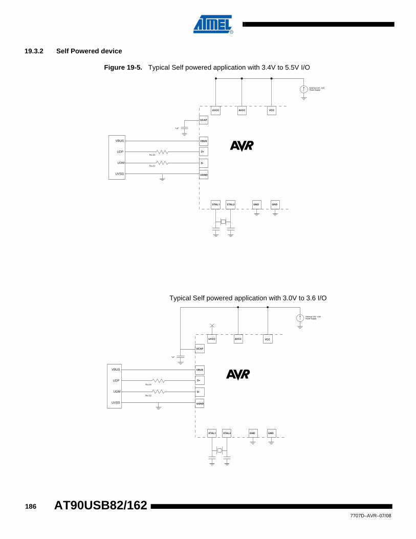
19.3.2 Self Powered device
Figure 19-5. Typical Self powered application with 3.4V to 5.5V I/O
Typical Self powered application with 3.0V to 3.6 I/O
1µF
External 3.4V - 5.5VPower Supply
UDP
UDM
VBUS
UVSS
UCAP
D-
D+
VBUS
UGND
UVCC AVCC VCC
XTAL1 XTAL2 GND GND
Rs=22
Rs=22
1µF
External 3.0V - 3.6VPower Supply
UDP
UDM
VBUS
UVSS
UCAP
D-
D+
VBUS
UGND
UVCC AVCC VCC
XTAL1 XTAL2 GND GND
Rs=22
Rs=22
1867707D–AVR–07/08
AT90USB82/162

AT90USB82/162
19.3.3 Design guidelines
• Serial resistors on USB Data lines must have 22 Ohms value (+/- 5%).
• Traces from the input USB receptable (or from the cable connection in the case of a tethered device) to the USB microcontroller pads should be as short as possibles, and follow differential traces routing rules (same length, as near as possible, avoid vias accumulation).
• Voltage transcient / ESD suppressors may also be used to prevent USB pads to be damaged by external disturbances.
• Ucap capacitor should be 1µF (+/- 10%) for correct operation.
• A 10µF capacitor is highly recommended on VBUS line
19.4 General Operating Modes
19.4.1 IntroductionThe USB controller is disabled and reset after a hardware reset generated by:
– Power on reset
– External reset
– Watchdog reset
– Brown out reset
– debugWIRE reset
But another available and optionnal reset source is :
– USB End Of Reset
In this case, the USB controller is reset, but not disabled (so that the device remains attached).
19.4.2 Power-on and resetThe next diagram explains the USB controller main states on power-on:
Figure 19-6. USB controller states after reset
When the USB controller is in reset state:
• USBE is not set
Dev ice
Reset
USBE=0 <any otherstate>
USBE=1
Clock stoppedFRZCLK=1
Macro off
USBE=0
USBE=0
HW RESET(excepted from EOR)
HW RESET from EOR
1877707D–AVR–07/08

• the USB controller clock is stopped in order to minimize the power consumption (FRZCLK=1),
• the USB controller is disabled,
• USB is in the suspend mode,
• the Device USB controllers internal state is reset.
• The DPACC bit and the DPADD10:0 field can be set by software. The DPRAM is not cleared.
• The SPDCONF bits can be set by software.
After setting USBE, the USB Controller enters in the Device state.
The USB Controller can at any time be ‘stopped’ by clearing USBE. In fact, clearing USBE acts as an hardware reset on the USB macro.
19.4.3 InterruptsTwo interrupts vectors are assigned to USB controller.
Figure 19-7. USB Interrupt System
The macro distinguishes between USB General events in opposition with USB Endpoints events that are relevant with data transfers relatives to each endpoint.
Figure 19-8. USB General interrupt vector sources
USB Device Interrupt
USB General Interrupt Vector
EndpointInterrupt
USB Endpoint/Pipe Interrupt Vector
UPRSMIUDINT.6
UPRSMEUDIEN.6
EORSMIUDINT.5
EORSMEUDIEN.5
WAKEUPI
UDINT.4WAKEUPE
UDIEN.4EORSTIUDINT.3
EORSTEUDIEN.3
SOFIUDINT.2
SOFEUDIEN.2
SUSPIUDINT.0
SUSPEUDIEN.0
USB General Interrupt Vector
Asynchronous Interrupt source(allows the CPU to wake up from power down mode)
1887707D–AVR–07/08
AT90USB82/162

AT90USB82/162
Each of these interupts are time-relative events that will be detected only if the USB clock is enabled (FRZCLK bit set), except for the WAKEUP interrupt that will trigger each time a state change is detected on the data lines.
This asynchronous interrupt WAKEUP allows to wake-up a device that is in power-down mode, generally after that the USB has entered the Suspend state.
Figure 19-9. USB Endpoint Interrupt vector sources
Each endpoint has 8 interrupts sources associated with flags, and each source can be enabled or not to trigger the corresponding endpoint interrupt.
If, for an endpoint, at least one of the sources is enabled to trigger interrupt, the corresponding event(s) will make the program branch to the USB Endpoint Interrupt vector. The user may determine the source (endpoint) of the interrupt by reading the UEINT register, and then handle the event detected by polling the different flags.
FLERREUEIENX.7
OVERFIUESTAX.6UNDERFIUESTAX.5
NAKINIUEINTX.6
NAKINEUEIENX.6
NAKOUTIUEINTX.4
TXSTPEUEIENX.4
RXSTPIUEINTX.3
TXOUTEUEIENX.3
RXOUTIUEINTX.2
RXOUTEUEIENX.2
STALLEDI
UEINTX.1STALLEDE
UEIENX.1
EPINTUEINT.X
Endpoint 0
Endpoint 1
Endpoint 2
Endpoint 3
Endpoint 4
TXINI
UEINTX.0TXINE
UEIENX.0
USB Endpoint Interrupt Vector
1897707D–AVR–07/08

19.5 Power modes
19.5.1 Idle modeIn this mode, the CPU core is halted (CPU clock stopped). The Idle mode is taken wether the USB controller is running or not. The CPU can wake up on any USB interrupts.
19.5.2 Power downIn this mode, the oscillator is stopped and halts all the clocks (CPU and peripherals). The USB controller “wakes up” when:
• the WAKEUPI interrupt is triggered (single asynchronous interrupt)
19.5.3 Freeze clockThe firmware has the ability to reduce the power consumption by setting the FRZCLK bit, which freeze the clock of USB controller. When FRZCLK is set, it is still possible to access to the fol-lowing registers:
• USBCON,
• DPRAM direct access registers (DPADD7:0, UEDATX)
• UDCON (detach, ...)
• UDINT
• UDIEN
Moreover, when FRZCLK is set, only the asynchronous interrupt may be triggered :
• WAKEUPI
19.6 Memory managementThe controller does only support the following memory allocation management.
The reservation of an Endpoint can only be made in the increasing order (Endpoint 0 to the last Endpoint). The firmware shall thus configure them in the same order.
The reservation of an Endpoint “ki” is done when its ALLOC bit is set. Then, the hardware allo-cates the memory and insert it between the Endpoints “ki-1” and “ki+1”. The “ki+1” Endpoint memory “slides” up and its data is lost. Note that the “ki+2” and upper Endpoint memory does not slide.
Clearing an Endpoint enable (EPEN) does not clear either its ALLOC bit, or its configuration (EPSIZE/PSIZE, EPBK/PBK). To free its memory, the firmware should clear ALLOC. Then, the “ki+1” Endpoint memory automatically “slides” down. Note that the “ki+2” and upper Endpoint memory does not slide.
The following figure illustrates the allocation and reorganization of the USB memory in a typical example:
1907707D–AVR–07/08
AT90USB82/162

AT90USB82/162
Table 19-1. Allocation and reorganization USB memory flow
• First, Endpoint 0 to Endpoint 4 are configured, in the growing order. The memory of each is reserved in the DPRAM.
• Then, the Endpoint 2is disabled (EPEN=0), but its memory reservation is internally kept by the controller.
• Its ALLOC bit is cleared: the Endpoint 3 “slides” down, but the Endpoint 4 does not “slide”.
• Finally, the firmware chooses to reconfigure the Endpoint 2, but with a bigger size. The controller reserved the memory after the endpoint 1 memory and automatically “slide” the Endpoint 3. The Endpoint 4 does not move and a memory conflict appear, in that both Endpoint 3 and 4 use a common area. The data of those endpoints are potentially lost.
Note that :
• the data of Endpoint 0 are never lost whatever the activation or deactivation of the higher Endpoint. Its data is lost if it is deactivated.
• Deactivate and reactivate the same Endpoint with the same parameters does not lead to a “slide” of the higher endpoints. For those endpoints, the data are preserved.
• CFGOK is set by hardware even in the case that there is a “conflict” in the memory allocation.
19.7 PAD suspendThe next figures illustrates the pad behaviour:
• In the “idle” mode, the pad is put in low power consumption mode.
• In the “active” mode, the pad is working.
Free memory
0
1
2
3
4
EPEN=1ALLOC=1
Free memory
0
1
EPEN=0(ALLOC=1)
4
3
Free memory
0
1
3
Lost memory
4
Endpointsactivation
Endpoint DisableFree its memory
(ALLOC=0)
Free memory
0
1
2 (bigger size)
EndpointActivatation
4Conflict
3
1917707D–AVR–07/08

Figure 19-10. Pad behaviour
The SUSPI flag indicated that a suspend state has been detected on the USB bus. This flag automatically put the USB pad in Idle. The detection of a non-idle event sets the WAKEUPI flag and wakes-up the USB pad.
Moreover, the pad can also be put in the “idle” mode if the DETACH bit is set. It come back in the active mode when the DETACH bit is cleared.
19.8 D+/D- Read/writeThe level of D+ and D- can be read and written using the UPOE register. The USB controller has to be enabled to write a value. For read operation, the USB controller can be enabled or disabled.
Idle mode
Active mode
USBE=1& DETACH=0& suspend
USBE=0| DETACH=1| suspend
SUSPI Suspend detected = USB pad power down Clear Suspend by software
Resume = USB pad wake-upClear Resume by softwareWAKEUPI
PAD statusActivePower DownActive
1927707D–AVR–07/08
AT90USB82/162

AT90USB82/162
19.9 Registers description
19.9.1 USB general registers
• 7 – USBE: USB macro Enable Bit Set to enable the USB controller. Clear to disable and reset the USB controller, to disable the USB transceiver and to disable the USB controller clock inputs.
• 6 – ReservedThe value read from this bit is always 0. Do not set this bit.
• 5 – FRZCLK: Freeze USB Clock BitSet to disable the clock inputs (the ”Resume Detection” is still active). This reduces the power consumption. Clear to enable the clock inputs.
• 4-0 – ReservedThe value read from these bits is always 0. Do not set these bits.
• 7 – DPACC: DPRAM Direct Access BitSet this bit to directly read the content the Dual-Port RAM (DPR) data through the UEDATX or UPDATX registers. See Section 19.6, page 190 for more details.
Clear this bit for normal operation and access the DPR through the endpoint FIFO.
• 6-0 – ReservedThe value read from these bits is always 0. Do not set these bits.
Bit 7 6 5 4 3 2 1 0
USBE - FRZLK - - - - - USBCON
Read/Write
R/W R R/W R R R R R
Initial Val-ue
0 0 1 0 0 0 0 0
Bit 7 6 5 4 3 2 1 0
DPACC - - - - - - - UDPAD-DH
Read/Write
R/W R R R R R R R
Initial Value
0 0 0 0 0 0 0 0
Bit 7 6 5 4 3 2 1 0
DPADD7:0 UDPAD-DL
Read/Write
R/W R/W R/W R/W R/W R/W R/W R/W
Initial Value
0 0 0 0 0 0 0 0
1937707D–AVR–07/08

• 7-0 – DPADD7:0: DPRAM Address Low BitDAPDD7:0 is the least significant part of DPADD.
19.9.2 USB/PS2 Software Output Enable register – UPOE
• Bit 7:6 – UPOE[1:0]: USB/PS2 Output enableSet these bits with the following configuration to enable or disable the USB/PS2 software drive.UPOE1 - UPOE00 - 0 : Direct drive is disabled.0 - 1 : Reserved1 - 0 : Direct drive of DP/DM with USB levels (UPDRV[1:0] values)1 - 1 : Direct drive of DP/DM with PS/2 levels (UPDRV[1:0] values)
• Bit 5:4 – UPDRV[1:0] : USB/PS2 direct drive valuesWrite in UPDRV1 the value to write on D+/SCK following the UPOE[1:0] configuration.
Write in UPDRV0 the value to write on D-/DATA following the UPOE[1:0] configuration.
• Bit 3 – SCKI : SCK Input valueThis bit is set to one by hardware if a ‘1’ is read on SCK (PS/2 pad). This bit is set to zero by hardware if a ‘0’ is read on SCK (PS/2 pad).
• Bit 2 – DATAI : DATA Input valueThis bit is set to one by hardware if a ‘1’ is read on DATA (PS/2 pad). This bit is set to zero by hardware if a ‘0’ is read on DATA (PS/2 pad).
• Bit 1 – DPI : D+ Input valueThis bit is set to one by hardware if a ‘1’ is read on D+ (USB pad). This bit is set to zero by hardware if a ‘0’ is read on D+ (USB pad).
• Bit 0 – DMI : D- Input valueThis bit is set to one by hardware if a ‘1’ is read on D- (USB pad). This bit is set to zero by hardware if a ‘0’ is read on D- (USB pad).
19.10 USB Software Operating modesDepending on the USB operating mode, the software should perform some the following operations:
Power On the USB interface
• Configure PLL interface
• Enable PLL
• Check PLL lock
Bit 7 6 5 4 3 2 1 0
UPWE1 UPWE0 UPDRV1
UPDRV0
SCKI DATAI DPI DMI UPOE
Read/Write R/W R/W R/W R/W R R R R
Initial Value 0 0 0 0 0 0 0 0
1947707D–AVR–07/08
AT90USB82/162

AT90USB82/162
• Enable USB interface
• Configure USB interface (USB Endpoint 0 configuration)
• Attach USB device
Power Off the USB interface
• Detach USB device
• Disable USB interface
• Disable PLL
Suspending the USB interface
• Clear Suspend Bit
• Set USB suspend clock
• Disable PLL
• Be sure to have interrupts enabled (WAKEUPE) to exit sleep mode
• Put the MCU in sleep mode
Resuming the USB interface
• Enable PLL
• Wait PLL lock
• Clear USB suspend clock
• Clear Resume information
1957707D–AVR–07/08

20. USB Device Operating modes
20.1 IntroductionThe USB device controller supports full speed data transfers. In addition to the default control endpoint, it provides four other endpoints, which can be configured in control, bulk, interrupt or isochronous modes:
• Endpoint 0:programmable size FIFO up to 64 bytes, default control endpoint
• Endpoints 1and 2:programmable size FIFO up to 64 bytes.
• Endpoints 3 and 4: programmable size FIFO up to 64 bytes with ping-pong mode.
The controller starts in the “idle” mode. In this mode, the pad consumption is reduced to the minimum.
20.2 Power-on and resetThe next diagram explains the USB device controller main states on power-on:
Figure 20-1. USB device controller states after reset
The reset state of the Device controller is:
• the macro clock is stopped in order to minimize the power consumption (FRZCLK set),
• the USB device controller internal state is reset (all the registers are reset to their default value. Note that DETACH is set.)
• the endpoint banks are reset
• the D+ pull up are not activated (mode Detach)
The D+ pull-up will be activated as soon as the DETACH bit is cleared.
The macro is in the ‘Idle’ state after reset with a minimum power consumption and does not need to have the PLL activated to enter in this state.
The USB device controller can at any time be reset by clearing USBE.
20.3 Endpoint resetAn endpoint can be reset at any time by setting in the UERST register the bit corresponding to the endpoint (EPRSTx). This resets:
• the internal state machine on that endpoint,
• the Rx and Tx banks are cleared and their internal pointers are restored,
Reset
Idle
HWRESET
USBE=0
<anyotherstate>
USBE=0
USBE=1UID=1
1967707D–AVR–07/08
AT90USB82/162

AT90USB82/162
• the UEINTX, UESTA0X and UESTA1X are restored to their reset value.
The data toggle field remains unchanged.
The other registers remain unchanged.
The endpoint configuration remains active and the endpoint is still enabled.
The endpoint reset may be associated with a clear of the data toggle command (RSTDT bit) as an answer to the CLEAR_FEATURE USB command.
20.4 USB resetWhen an USB reset is detected on the USB line (SEO state with a minimal duration of 100µs), the next operations are performed by the controller:
• all the endpoints are disabled
• the default control endpoint remains configured
• The data toggle of the default control endpoint is cleared.
If the hardware reset function is selected, a reset is generated to the CPU core without disabling the USB controller (that remains in the same state than after a USB Reset).
20.5 Endpoint selectionPrior to any operation performed by the CPU, the endpoint must first be selected. This is done by setting the EPNUM2:0 bits (in UENUM register) with the endpoint number which will be man-aged by the CPU.
The CPU can then access to the various endpoint registers and data.
20.6 Endpoint activationThe endpoint is maintained under reset as long as the EPEN bit is not set.
The following flow must be respected in order to activate an endpoint:
1977707D–AVR–07/08

Figure 20-2. Endpoint activation flow:
As long as the endpoint is not correctly configured (CFGOK cleared), the hardware does not acknowledge the packets sent by the host.
CFGOK will not be set if the Endpoint size parameter is bigger than the DPRAM size.
A clear of EPEN acts as an endpoint reset (see Section 20.3, page 196 for more details). It also performs the next operation:
• The configuration of the endpoint is kept (EPSIZE, EPBK, ALLOC kept)
• It resets the data toggle field.
• The DPRAM memory associated to the endpoint is still reserved.
See Section 19.6, page 190 for more details about the memory allocation/reorganization.
20.7 Address SetupThe USB device address is set up according to the USB protocol:
• the USB device, after power-up, responds at address 0
• the host sends a SETUP command (SET_ADDRESS(addr)),
• the firmware records that address in UADD, but keep ADDEN cleared,
• the USB device sends an IN command of 0 bytes (IN 0 Zero Length Packet) to acknowledge the transaction,
• then, the firmware may enable the USB device address by setting ADDEN. The only accepted address by the controller is the one stored in UADD.
ADDEN and UADD shall not be written at the same time.
UADD contains the default address 00h after a power-up or an USB reset.
EndpointActivation
CFGOK=1
ERROR
NoYes
Endpoint activated
Activate the endpoint
Select the endpoint
EPEN=1
UENUMEPNUM=x
Test the correct endpointconfiguration
UECFG1XALLOCEPSIZEEPBK
Configure:- the endpoint size- the bank parametrization
Allocation and reorganization ofthe memory is made on-the-fly
UECFG0XEPDIR
EPTYPE...
Configure:- the endpoint direction- the endpoint type- the Not Yet Disable feature
1987707D–AVR–07/08
AT90USB82/162

AT90USB82/162
ADDEN is cleared by hardware:
• after a power-up reset,
• when an USB reset is received,
• or when the macro is disabled (USBE cleared)
When this bit is cleared, the default device address 00h is used.
20.8 Suspend, Wake-up and ResumeAfter a period of 3 ms during which the USB line was inactive (J state), the controller setn the SUSPI flag and triggers the corresponding interrupt if enabled. The firmware may then set the FRZCLK bit.
The CPU can also, depending on software architecture, disable the PLL and/or enter in the idle mode to reduce the power consumption (especially in a bus powered application).
There are two ways to recover from the “Suspend” mode:
• First one is to clear the FRZCLK bit. This is possible if the CPU is not in the Idle mode.
• Second way, if the CPU is “idle”, is to enable the WAKEUPI interrupt (WAKEUPE set). Then, as soon as an non-idle signal is seen by the controller, the WAKEUPI interrupt is triggered. The firmware shall then clear the FRZCLK bit to restart the transfer.
There are no relationship between the SUSPI interrupt and the WAKEUPI interrupt: the WAKE-UPI interrupt is triggered as soon as there are non-idle patterns on the data lines. Thus, the WAKEUPI interrupt can occurs even if the controller is not in the “suspend” mode.
When the WAKEUPI interrupt is triggered, if the SUSPI interrupt bit was already set, it is cleared by hardware.
When the SUSPI interrupt is triggered, if the WAKEUPI interrupt bit was already set, it is cleared by hardware.
20.9 DetachThe reset value of the DETACH bit is 1.
It is possible to re-enumerate a device, simply by setting and clearing the DETACH bit (the line discharge time must be taken in account).
• When the USB device controller is in full-speed mode, setting DETACH will disconnect the pull-up on the D+ . Then, clearing DETACH will connect the pull-up on the D+.
Figure 20-3. Detach a device in Full-speed:
EN=1
D +
UVREF
D -
Detach, thenAttach EN=1
D +
UVREF
D -
1997707D–AVR–07/08

20.10 Remote Wake-upThe “Remote Wake-up” (or “upstream resume”) request is the only operation allowed to be sent by the device on its own initiative. Anyway, to do that, the device should first have received a DEVICE_REMOTE_WAKEUP request from the host.
• First, the USB controller must have detected the “suspend” state of the line: the remote wake-up can only be sent if the SUSPI bit is set.
• The firmware has then the ability to set RMWKUP to send the “upstream resume” stream. This will automatically be done by the controller after 5ms of inactivity on the USB line.
• When the controller starts to send the “upstream resume”, the UPRSMI flag is set and interrupt is triggered (if enabled). If SUSPI was set, SUSPI is cleared by hardware.
• RMWKUP is automatically cleared by hardware at the end of the “upstream resume”.
• After that, if the controller detects a good “End Of Resume” signal from the host, an EORSMI interrupt is triggered (if enabled).
20.11 STALL requestFor each endpoint, the STALL management is performed using 2 bits:
– STALLRQ (enable stall request)
– STALLRQC (disable stall request)
– STALLEDI (stall sent interrupt)
To send a STALL handshake at the next request, the STALLRQ request bit has to be set. All fol-lowing requests will be handshak’ed with a STALL until the STALLRQC bit is set.
Setting STALLRQC automatically clears the STALLRQ bit. The STALLRQC bit is also immedi-ately cleared by hardware after being set by software. Thus, the firmware will never read this bit as set.
Each time the STALL handshake is sent, the STALLEDI flag is set by the USB controller and the EPINTx interrupt will be triggered (if enabled).
The incoming packets will be discarded (RXOUTI and RWAL will not be set).
The host will then send a command to reset the STALL: the firmware just has to set the STALL-RQC bit and to reset the endpoint.
20.11.1 Special consideration for Control EndpointsA SETUP request is always ACK’ed.
If a STALL request is set for a Control Endpoint and if a SETUP request occurs, the SETUP request has to be ACK’ed and the STALLRQ request and STALLEDI sent flags are automati-cally reset (RXSETUPI set, TXIN cleared, STALLED cleared, TXINI cleared...).
This management simplifies the enumeration process management. If a command is not sup-ported or contains an error, the firmware set the STALL request flag and can return to the main task, waiting for the next SETUP request.
This funct ion is compl iant wi th the Chapter 8 test that sends extra status for a GET_DESCRIPTOR. The firmware sets the STALL request just after receiving the status. All extra status will be automatically STALL’ed until the next SETUP request.
2007707D–AVR–07/08
AT90USB82/162

AT90USB82/162
20.11.2 STALL handshake and Retry mechanismThe Retry mechanism has priority over the STALL handshake. A STALL handshake is sent if the STALLRQ request bit is set and if there is no retry required.
20.12 CONTROL endpoint managementA SETUP request is always ACK’ed. When a new setup packet is received, the RXSTPI inter-rupt is triggered (if enabled). The RXOUTI interrupt is not triggered.
The FIFOCON and RWAL fields are irrelevant with CONTROL endpoints. The firmware shall thus never use them on that endpoints. When read, their value is always 0.
CONTROL endpoints are managed by the following bits:
• RXSTPI is set when a new SETUP is received. It shall be cleared by firmware to acknowledge the packet and to clear the endpoint bank.
• RXOUTI is set when a new OUT data is received. It shall be cleared by firmware to acknowledge the packet and to clear the endpoint bank.
• TXINI is set when the bank is ready to accept a new IN packet. It shall be cleared by firmware to send the packet and to clear the endpoint bank.
CONTROL endpoints should not be managed by interrupts, but only by polling the status bits.
20.12.1 Control WriteThe next figure shows a control write transaction. During the status stage, the controller will not necessary send a NAK at the first IN token:
• If the firmware knows the exact number of descriptor bytes that must be read, it can then anticipate on the status stage and send a ZLP for the next IN token,
• or it can read the bytes and poll NAKINI, which tells that all the bytes have been sent by the host, and the transaction is now in the status stage.
SETUP
RXSTPI
RXOUTI
TXINI
USB line
HW SW
OUT
HW SW
OUT
HW SW
IN IN
NAK
SW
DATASETUP STATUS
2017707D–AVR–07/08

20.12.2 Control ReadThe next figure shows a control read transaction. The USB controller has to manage the simulta-neous write requests from the CPU and the USB host:
A NAK handshake is always generated at the first status stage command.
When the controller detect the status stage, all the data writen by the CPU are erased, and clearing TXINI has no effects.
The firmware checks if the transmission is complete or if the reception is complete.
The OUT retry is always ack’ed. This reception:
- set the RXOUTI flag (received OUT data)
- set the TXINI flag (data sent, ready to accept new data)
software algorithm:
set transmit ready
wait (transmit complete OR Receive complete)
if receive complete, clear flag and return
if transmit complete, continue
Once the OUT status stage has been received, the USB controller waits for a SETUP request. The SETUP request have priority over any other request and has to be ACK’ed. This means that any other flag should be cleared and the fifo reset when a SETUP is received.
WARNING: the byte counter is reset when a OUT Zero Length Packet is received. The firmware has to take care of this.
20.13 OUT endpoint managementOUT packets are sent by the host. All the data can be read by the CPU, which acknowledges or not the bank when it is empty.
20.13.1 OverviewThe Endpoint must be configured first.
SETUP
RXSTPI
RXOUTI
TXINI
USB line
HW SW
IN
HW SW
IN OUT OUT
NAK
SW
SW
HW
Wr EnableHOST
Wr EnableCPU
DATASETUP STATUS
2027707D–AVR–07/08
AT90USB82/162

AT90USB82/162
20.13.1.1 “Manual” modeEach time the current bank is full, the RXOUTI and the FIFOCON bits are set. This triggers an interrupt if the RXOUTE bit is set. The firmware can acknowledge the USB interrupt by clearing the RXOUTI bit. The Firmware read the data and clear the FIFOCON bit in order to free the cur-rent bank. If the OUT Endpoint is composed of multiple banks, clearing the FIFOCON bit will switch to the next bank. The RXOUTI and FIFOCON bits are then updated by hardware in accordance with the status of the new bank.
RXOUTI shall always be cleared before clearing FIFOCON.
The RWAL bit always reflects the state of the current bank. This bit is set if the firmware can read data from the bank, and cleared by hardware when the bank is empty.
20.13.2 Detailed descriptionThe data are read by the CPU, following the next flow:
• When the bank is filled by the host, an endpoint interrupt (EPINTx) is triggered, if enabled (RXOUTE set) and RXOUTI is set. The CPU can also poll RXOUTI or FIFOCON, depending on the software architecture,
• The CPU acknowledges the interrupt by clearing RXOUTI,
• The CPU can read the number of byte (N) in the current bank (N=BYCT),
• The CPU can read the data from the current bank (“N” read of UEDATX),
OUTDATA
(to bank 0)ACK
RXOUTI
FIFOCON
HW
OUTDATA
(to bank 0)ACK
HW
SW
SW
SW
Example with 1 OUT data bank
read data from CPUBANK 0
OUTDATA
(to bank 0)ACK
RXOUTI
FIFOCON
HW
OUTDATA
(to bank 1)ACK
SW
SW
Example with 2 OUT data banks
read data from CPUBANK 0
HWSW
read data from CPUBANK 0
read data from CPUBANK 1
NAK
2037707D–AVR–07/08

• The CPU can free the bank by clearing FIFOCON when all the data is read, that is:
• after “N” read of UEDATX,
• as soon as RWAL is cleared by hardware.
If the endpoint uses 2 banks, the second one can be filled by the HOST while the current one is being read by the CPU. Then, when the CPU clear FIFOCON, the next bank may be already ready and RXOUTI is set immediately.
20.14 IN endpoint managementIN packets are sent by the USB device controller, upon an IN request from the host. All the data can be written by the CPU, which acknowledge or not the bank when it is full.Overview
The Endpoint must be configured first.
20.14.0.1 “Manual” modeThe TXINI bit is set by hardware when the current bank becomes free. This triggers an interrupt if the TXINE bit is set. The FIFOCON bit is set at the same time. The CPU writes into the FIFO and clears the FIFOCON bit to allow the USB controller to send the data. If the IN Endpoint is composed of multiple banks, this also switches to the next data bank. The TXINI and FIFOCON bits are automatically updated by hardware regarding the status of the next bank.
TXINI shall always be cleared before clearing FIFOCON.
2047707D–AVR–07/08
AT90USB82/162

AT90USB82/162
The RWAL bit always reflects the state of the current bank. This bit is set if the firmware can write data to the bank, and cleared by hardware when the bank is full.
20.14.1 Detailed descriptionThe data are written by the CPU, following the next flow:
• When the bank is empty, an endpoint interrupt (EPINTx) is triggered, if enabled (TXINE set) and TXINI is set. The CPU can also poll TXINI or FIFOCON, depending the software architecture choice,
• The CPU acknowledges the interrupt by clearing TXINI,
• The CPU can write the data into the current bank (write in UEDATX),
• The CPU can free the bank by clearing FIFOCON when all the data are written, that is:
• after “N” write into UEDATX
• as soon as RWAL is cleared by hardware.
If the endpoint uses 2 banks, the second one can be read by the HOST while the current is being written by the CPU. Then, when the CPU clears FIFOCON, the next bank may be already ready (free) and TXINI is set immediately.
20.14.1.1 AbortAn “abort” stage can be produced by the host in some situations:
INDATA
(bank 0)ACK
TXINI
FIFOCON
HW
Example with 1 IN data bank
write data from CPUBANK 0
Example with 2 IN data banks
SW
SW SW
SW
IN
INDATA
(bank 0)ACK
TXINI
FIFOCON write data from CPUBANK 0
SW
SW SW
SW
INDATA
(bank 1)ACK
write data from CPUBANK 0
write data from CPUBANK 1
SW
HW
write data from CPUBANK0
NAK
2057707D–AVR–07/08

• In a control transaction: ZLP data OUT received during a IN stage,
• In an isochronous IN transaction: ZLP data OUT received on the OUT endpoint during a IN stage on the IN endpoint
• ...
The KILLBK bit is used to kill the last “written” bank. The best way to manage this abort is to per-form the following operations:
Table 20-1. Abort flow
20.15 Isochronous mode
20.15.1 UnderflowAn underflow can occur during IN stage if the host attempts to read a bank which is empty. In this situation, the UNDERFI interrupt is triggered.
An underflow can also occur during OUT stage if the host send a packet while the banks are already full. Typically, he CPU is not fast enough. The packet is lost.
It is not possible to have underflow error during OUT stage, in the CPU side, since the CPU should read only if the bank is ready to give data (RXOUTI=1 or RWAL=1)
20.15.2 CRC ErrorA CRC error can occur during OUT stage if the USB controller detects a bad received packet. In this situation, the STALLEDI interrupt is triggered. This does not prevent the RXOUTI interrupt from being triggered.
20.16 OverflowIn Control, Isochronous, Bulk or Interrupt Endpoint, an overflow can occur during OUT stage, if the host attempts to write in a bank that is too small for the packet. In this situation, the OVERFI interrupt is triggered (if enabled). The packet is hacknowledged and the RXOUTI interrupt is also triggered (if enabled). The bank is filled with the first bytes of the packet.
EndpointAbort
Abort done
Abort is based on the factthat no banks are busy,meaning that nothing has tobe sent.
Disable the TXINI interrupt.
Endpointreset
NBUSYBK=0
Yes
ClearUEIENX.TXINE
No
KILLBK=1
KILLBK=1Yes
Kill the last writtenbank.
Wait for the end of theprocedure.
No
2067707D–AVR–07/08
AT90USB82/162

AT90USB82/162
It is not possible to have overflow error during IN stage, in the CPU side, since the CPU should write only if the bank is ready to access data (TXINI=1 or RWAL=1).
20.17 InterruptsThe next figure shows all the interrupts sources:
Figure 20-4. USB Device Controller Interrupt System
There are 2 kind of interrupts: processing (i.e. their generation are part of the normal processing) and exception (errors).
Processing interrupts are generated when:
• Upstream resume(UPRSMI)
• End of resume(EORSMI)
• Wake up(WAKEUPI)
• End of reset (Speed Initialization)(EORSTI)
• Start of frame(SOFI, if FNCERR=0)
• Suspend detected after 3 ms of inactivity(SUSPI)
Exception Interrupts are generated when:
• CRC error in frame number of SOF(SOFI, FNCERR=1)
UPRSMIUDINT.6
UPRSMEUDIEN.6
EORSMIUDINT.5
EORSMEUDIEN.5
WAKEUPI
UDINT.4WAKEUPE
UDIEN.4EORSTIUDINT.3
EORSTEUDIEN.3
SOFIUDINT.2
SOFEUDIEN.2
SUSPIUDINT.0
SUSPEUDIEN.0
USB Device Interrupt
2077707D–AVR–07/08

Figure 20-5. USB Device Controller Endpoint Interrupt System
Processing interrupts are generated when:
• Ready to accept IN data(EPINTx, TXINI=1)
• Received OUT data(EPINTx, RXOUTI=1)
• Received SETUP(EPINTx, RXSTPI=1)
Exception Interrupts are generated when:
• Stalled packet(EPINTx, STALLEDI=1)
• CRC error on OUT in isochronous mode(EPINTx, STALLEDI=1)
• Overflow(EPINTx, OVERFI=1)
• Underflow in isochronous mode(EPINTx, UNDERFI=1)
• NAK IN sent(EPINTx, NAKINI=1)
• NAK OUT sent(EPINTx, NAKOUTI=1)
20.18 Registers
20.18.1 USB device general registers
EPINTUEINT.X
Endpoint 0
Endpoint 1
Endpoint 2
Endpoint 3
Endpoint 4
Endpoint Interrupt
FLERREUEIENX.7
OVERFIUESTAX.6UNDERFIUESTAX.5
NAKINIUEINTX.6
NAKINEUEIENX.6
NAKOUTIUEINTX.4
TXSTPEUEIENX.4
RXSTPIUEINTX.3
TXOUTEUEIENX.3
RXOUTIUEINTX.2
RXOUTEUEIENX.2
STALLEDI
UEINTX.1STALLEDE
UEIENX.1TXINI
UEINTX.0TXINE
UEIENX.0
Bit 7 6 5 4 3 2 1 0
- - - - - RSTCPU RMWKUP DETACH UDCON
Read/Write
R R R R R R/W R/W R/W
Initial Value
0 0 0 0 0 0 0 1
2087707D–AVR–07/08
AT90USB82/162

AT90USB82/162
• Bit 2- RSTCPU - USB Reset CPU BitSet this bit to one by firmware in order to reset the CPU at the next USB reset (without disabling the USB controller). The value of this bit will not be affected by the reset of the CPU generated by a End Of Reset (remains set). This bit is reset when the USB controller is disabled.
Set this bit to zero by firmware otherwise.
• Bit 1- RMWKUP - Remote Wake-up BitSet to send an “upstream-resume” to the host for a remote wake-up. The SUSPI bit must be set to allow the remote wake up to be sent.
Cleared by hardware. Clearing by software has no effect.
See Section 20.10, page 200 for more details.
• Bit 0 - DETACH - Detach BitSet to physically detach de device.
Clear to reconnect the device. See Section 20.9, page 199 for more details.
• 7 - ReservedThe value read from these bits is always 0. Do not set these bits.
• 6 - UPRSMI - Upstream Resume Interrupt FlagSet by hardware when the USB controller is sending a resume signal called “Upstream Resume”. This triggers an USB interrupt if UPRSME is set.
Shall be cleared by software (USB clocks must be enabled before). Setting by software has no effect.
• 5 - EORSMI - End Of Resume Interrupt FlagSet by hardware when the USB controller detects a good “End Of Resume” signal initiated by the host. This triggers an USB interrupt if EORSME is set.
Shall be cleared by software. Setting by software has no effect.
• 4 - WAKEUPI - Wake-up CPU Interrupt FlagSet by hardware when the USB controller is re-activated by a filtered non-idle signal from the lines (not by an upstream resume). This triggers an interrupt if WAKEUPE is set.
Shall be cleared by software (USB clock inputs must be enabled before). Setting by software has no effect.
See Section 20.8, page 199 for more details.
Bit 7 6 5 4 3 2 1 0
- UPRSMI EORSMI WAKEUPI EORSTI SOFI - SUSPI UDINT
Read/Write
R R/W R/W R/W R/W R/W R R/W
Initial Value
0 0 0 0 0 0 0 0
2097707D–AVR–07/08

• 3 - EORSTI - End Of Reset Interrupt FlagSet by hardware when an “End Of Reset” has been detected by the USB controller. This triggers an USB interrupt if EORSTE is set.
Shall be cleared by software. Setting by software has no effect.
• 2 - SOFI - Start Of Frame Interrupt FlagSet by hardware when an USB “Start Of Frame” PID (SOF) has been detected (every 1 ms). This triggers an USB interrupt if SOFE is set..
• 1 - Reserved
• 0 - SUSPI - Suspend Interrupt FlagSet by hardware when an USB “Suspend” ‘idle bus for 3 frame periods: a J state for 3 ms) is detected. This triggers an USB interrupt if SUSPE is set.
Shall be cleared by software. Setting by software has no effect.
See Section 20.8, page 199 for more details.
The interrupt flags bits are set even if their corresponding ‘Enable’ bits is not set.
• 7 - ReservedThe value read from these bits is always 0. Do not set these bits.
• 6 - UPRSME - Upstream Resume Interrupt Enable BitSet to enable the UPRSMI interrupt.
Clear to disable the UPRSMI interrupt.
• 5 - EORSME - End Of Resume Interrupt Enable BitSet to enable the EORSMI interrupt.
Clear to disable the EORSMI interrupt.
• 4 - WAKEUPE - Wake-up CPU Interrupt Enable BitSet to enable the WAKEUPI interrupt.
Clear to disable the WAKEUPI interrupt.
• 3 - EORSTE - End Of Reset Interrupt Enable BitSet to enable the EORSTI interrupt. This bit is set after a reset.
Clear to disable the EORSTI interrupt.
• 2 - SOFE - Start Of Frame Interrupt Enable BitSet to enable the SOFI interrupt.
Bit 7 6 5 4 3 2 1 0
- UPRSME EORSME WAKEUPE EORSTE SOFE - SUSPE UDIEN
Read/Write
R R/W R/W R/W R/W R/W R R/W
Initial Value
0 0 0 0 0 0 0 0
2107707D–AVR–07/08
AT90USB82/162

AT90USB82/162
Clear to disable the SOFI interrupt.
• 1 - Reserved
• 0 - SUSPE - Suspend Interrupt Enable BitSet to enable the SUSPI interrupt.
Clear to disable the SUSPI interrupt.
• 7 - ADDEN - Address Enable BitSet to activate the UADD (USB address).
Cleared by hardware. Clearing by software has no effect.
See Section 20.7, page 198 for more details.
• 6-0 - UADD6:0 - USB Address BitsSet to configure the device address.
Shall not be cleared.
• 7-3 - ReservedThe value read from these bits is always 0. Do not set these bits.
• 2-0 - FNUM10:8 - Frame Number Upper FlagSet by hardware. These bits are the 3 MSB of the 11-bits Frame Number information. They are provided in the last received SOF packet. FNUM is updated if a corrupted SOF is received.
• 7-0 Frame Number Lower FlagSet by hardware. These bits are the 8 LSB of the 11-bits Frame Number information.
Bit 7 6 5 4 3 2 1 0
ADDEN UADD6:0 UDADDR
Read/Write
R/W R/W R R R R R R
Initial Value
0 0 0 0 0 0 0 0
Bit 7 6 5 4 3 2 1 0
- - - - - FNUM10:8 UDFNUMH
Read/Write
R R R R R R R R
Initial Value
0 0 0 0 0 0 0 0
Bit 7 6 5 4 3 2 1 0
FNUM7:0 UDFNUML
Read/Write
R R R R R R R R
Initial Value
0 0 0 0 0 0 0 0
2117707D–AVR–07/08

• 7-5 - ReservedThe value read from these bits is always 0. Do not set these bits.
• 4 - FNCERR -Frame Number CRC Error FlagSet by hardware when a corrupted Frame Number in start of frame packet is received.
This bit and the SOFI interrupt are updated at the same time.
• 3-0 - ReservedThe value read from these bits is always 0. Do not set these bits.
20.18.2 USB device endpoint registers
• 7-3 - ReservedThe value read from these bits is always 0. Do not set these bits.
• 2-0 - EPNUM2:0 Endpoint Number BitsSet to select the number of the endpoint which shall be accessed by the CPU. See Section 20.5, page 197 for more details.
Values greater than 100b are forbidden.
• 7-5 - ReservedThe value read from these bits is always 0. Do not set these bits.
• 4-0 - EPRST4:0 - Endpoint FIFO Reset BitsSet to reset the selected endpoint FIFO prior to any other operation, upon hardware reset or when an USB bus reset has been received. See Section 20.3, page 196 for more information
Bit 7 6 5 4 3 2 1 0
- - - FNCERR - - - - UDMFN
Read/Write
R R R R/W R R R R
Initial Value
0 0 0 0 0 0 0 0
Bit 7 6 5 4 3 2 1 0
- - - - - EPNUM2:0 UENUM
Read/Write
R R R R R R/W R/W R/W
Initial Value
0 0 0 0 0 0 0 0
Bit 7 6 5 4 3 2 1 0
- - - EPRST D4 EPRST D3 EPRST D2 EPRST D1 EPRST D0 UERST
Read/Write
R R R R/W R/W R/W R/W R/W
Initial Value
0 0 0 0 0 0 0 0
2127707D–AVR–07/08
AT90USB82/162
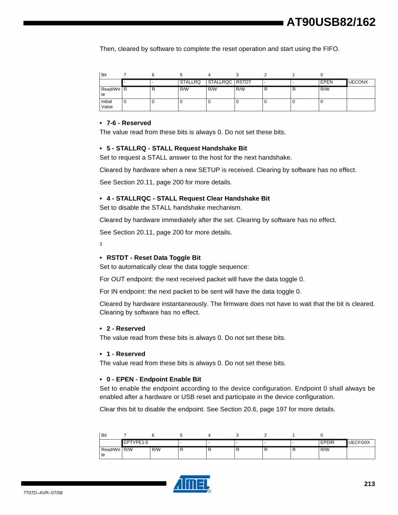
AT90USB82/162
Then, cleared by software to complete the reset operation and start using the FIFO.
• 7-6 - ReservedThe value read from these bits is always 0. Do not set these bits.
• 5 - STALLRQ - STALL Request Handshake BitSet to request a STALL answer to the host for the next handshake.
Cleared by hardware when a new SETUP is received. Clearing by software has no effect.
See Section 20.11, page 200 for more details.
• 4 - STALLRQC - STALL Request Clear Handshake BitSet to disable the STALL handshake mechanism.
Cleared by hardware immediately after the set. Clearing by software has no effect.
See Section 20.11, page 200 for more details.
3
• RSTDT - Reset Data Toggle BitSet to automatically clear the data toggle sequence:
For OUT endpoint: the next received packet will have the data toggle 0.
For IN endpoint: the next packet to be sent will have the data toggle 0.
Cleared by hardware instantaneously. The firmware does not have to wait that the bit is cleared. Clearing by software has no effect.
• 2 - ReservedThe value read from these bits is always 0. Do not set these bits.
• 1 - ReservedThe value read from these bits is always 0. Do not set these bits.
• 0 - EPEN - Endpoint Enable BitSet to enable the endpoint according to the device configuration. Endpoint 0 shall always be enabled after a hardware or USB reset and participate in the device configuration.
Clear this bit to disable the endpoint. See Section 20.6, page 197 for more details.
Bit 7 6 5 4 3 2 1 0
- - STALLRQ STALLRQC RSTDT - - EPEN UECONX
Read/Write
R R R/W R/W R/W R R R/W
Initial Value
0 0 0 0 0 0 0 0
Bit 7 6 5 4 3 2 1 0
EPTYPE1:0 - - - - - EPDIR UECFG0X
Read/Write
R/W R/W R R R R R R/W
2137707D–AVR–07/08

• 7-6 - EPTYPE1:0 - Endpoint Type BitsSet this bit according to the endpoint configuration:
00b: Control10b: Bulk
01b: Isochronous11b: Interrupt
• 5-1 - ReservedThe value read from these bits is always 0. Do not set these bits.
• 0 - EPDIR - Endpoint Direction BitSet to configure an IN direction for bulk, interrupt or isochronous endpoints.
Clear to configure an OUT direction for bulk, interrupt, isochronous or control endpoints.
• 7 - ReservedThe value read from these bits is always 0. Do not set these bits.
• 6-4 - EPSIZE2:0 - Endpoint Size BitsSet this bit according to the endpoint size:
000b: 8 bytes
001b: 16 bytes
010b: 32 bytes
011b: 64 bytes
Other : Reserved. Do not use this configuration.
• 3-2 - EPBK1:0 - Endpoint Bank BitsSet this field according to the endpoint size:
00b: One bank
01b: Double bank
1xb: Reserved. Do not use this configuration.
• 1 - ALLOC - Endpoint Allocation BitSet this bit to allocate the endpoint memory.
Clear to free the endpoint memory.
See Section 20.6, page 197 for more details.
Initial Value
0 0 0 0 0 0 0 0
Bit 7 6 5 4 3 2 1 0
- EPSIZE2:0 EPBK1:0 ALLOC - UECFG1X
Read/Write
R R/W R/W R/W R/W R/W R/W R
Initial Value
0 0 0 0 0 0 0 0
Bit 7 6 5 4 3 2 1 0
2147707D–AVR–07/08
AT90USB82/162

AT90USB82/162
• 0 - ReservedThe value read from these bits is always 0. Do not set these bits.
• 7 - CFGOK - Configuration Status FlagSet by hardware when the endpoint X size parameter (EPSIZE) and the bank parametrization (EPBK) are correct compared to the max FIFO capacity and the max number of allowed bank. This bit is updated when the bit ALLOC is set.
If this bit is cleared, the user should reprogram the UECFG1X register with correct EPSIZE and EPBK values.
• 6 - OVERFI - Overflow Error Interrupt FlagSet by hardware when an overflow error occurs in an isochronous endpoint. An interrupt (EPINTx) is triggered (if enabled).
See Section 20.15, page 206 for more details.
Shall be cleared by software. Setting by software has no effect.
• 5 - UNDERFI - Flow Error Interrupt FlagSet by hardware when an underflow error occurs in an isochronous endpoint. An interrupt (EPINTx) is triggered (if enabled).
See Section 20.15, page 206 for more details.
Shall be cleared by software. Setting by software has no effect.
• 4- ReservedThe value read from these bits is always 0. Do not set these bits.
• 3-2 - DTSEQ1:0 - Data Toggle Sequencing FlagSet by hardware to indicate the PID data of the current bank:
00b Data0
01b Data1
1xb Reserved.
For OUT transfer, this value indicates the last data toggle received on the current bank.
For IN transfer, it indicates the Toggle that will be used for the next packet to be sent. This is not relative to the current bank.
• 1-0 - NBUSYBK1:0 - Busy Bank FlagSet by hardware to indicate the number of busy bank.
For IN endpoint, it indicates the number of busy bank(s), filled by the user, ready for IN transfer.
Bit 7 6 5 4 3 2 1 0
CFGOK OVERFI UNDERFI - DTSEQ1:0 NBUSYBK1:0 UESTA0X
Read/Write
R R/W R/W R R R R R
Initial Value
0 0 0 0 0 0 0 0
2157707D–AVR–07/08

For OUT endpoint, it indicates the number of busy bank(s) filled by OUT transaction from the host.
00b All banks are free
01b 1 busy bank
10b 2 busy banks
11b Reserved.
• 7-3 - ReservedThe value read from these bits is always 0. Do not set these bits.
• 2 - CTRLDIR - Control Direction (Flag, and bit for debug purpose)Set by hardware after a SETUP packet, and gives the direction of the following packet:
- 1 for IN endpoint
- 0 for OUT endpoint.
Can not be set or cleared by software.
• 1-0 - CURRBK1:0 - Current Bank (all endpoints except Control endpoint) FlagSet by hardware to indicate the number of the current bank:
00b Bank0
01b Bank1
1xb Reserved.
Can not be set or cleared by software.
• 7 - FIFOCON - FIFO Control BitFor OUT and SETUP Endpoint:
Set by hardware when a new OUT message is stored in the current bank, at the same time than RXOUT or RXSTP.
Clear to free the current bank and to switch to the following bank. Setting by software has no effect.
Bit 7 6 5 4 3 2 1 0
- - - - - CTRLDIR CURRBK1:0 UESTA1X
Read/Write
R R R R R R R
Initial Value
0 0 0 0 0 0 0 0
Bit 7 6 5 4 3 2 1 0
FIFOCON NAKINI RWAL NAKOUTI RXSTPI RXOUTI STALLEDI TXINI UEINTX
Read/Write
R/W R/W R/W R/W R/W R/W R/W R/W
Initial Value
0 0 0 0 0 0 0 0
2167707D–AVR–07/08
AT90USB82/162

AT90USB82/162
For IN Endpoint:
Set by hardware when the current bank is free, at the same time than TXIN.
Clear to send the FIFO data and to switch the bank. Setting by software has no effect.
• 6 - NAKINI - NAK IN Received Interrupt FlagSet by hardware when a NAK handshake has been sent in response of a IN request from the host. This triggers an USB interrupt if NAKINE is sent.
Shall be cleared by software. Setting by software has no effect.
• 5 - RWAL - Read/Write Allowed FlagSet by hardware to signal:
- for an IN endpoint: the current bank is not full i.e. the firmware can push data into the FIFO,
- for an OUT endpoint: the current bank is not empty, i.e. the firmware can read data from the FIFO.
The bit is never set if STALLRQ is set, or in case of error.
Cleared by hardware otherwise.
This bit shall not be used for the control endpoint.
• 4 - NAKOUTI - NAK OUT Received Interrupt FlagSet by hardware when a NAK handshake has been sent in response of a OUT/PING request from the host. This triggers an USB interrupt if NAKOUTE is sent.
Shall be cleared by software. Setting by software has no effect.
• 3 - RXSTPI - Received SETUP Interrupt FlagSet by hardware to signal that the current bank contains a new valid SETUP packet. An inter-rupt (EPINTx) is triggered (if enabled).
Shall be cleared by software to handshake the interrupt. Setting by software has no effect.
This bit is inactive (cleared) if the endpoint is an IN endpoint.
• 2 - RXOUTI / KILLBK - Received OUT Data Interrupt FlagSet by hardware to signal that the current bank contains a new packet. An interrupt (EPINTx) is triggered (if enabled).
Shall be cleared by software to handshake the interrupt. Setting by software has no effect.
Kill Bank IN Bit
Set this bit to kill the last written bank.
Cleared by hardware when the bank is killed. Clearing by software has no effect.
See page 205 for more details on the Abort.
• 1 - STALLEDI - STALLEDI Interrupt FlagSet by hardware to signal that a STALL handshake has been sent, or that a CRC error has been detected in a OUT isochronous endpoint.
Shall be cleared by software. Setting by software has no effect.
2177707D–AVR–07/08

• 0 - TXINI - Transmitter Ready Interrupt FlagSet by hardware to signal that the current bank is free and can be filled. An interrupt (EPINTx) is triggered (if enabled).
Shall be cleared by software to handshake the interrupt. Setting by software has no effect.
This bit is inactive (cleared) if the endpoint is an OUT endpoint.
• 7 - FLERRE - Flow Error Interrupt Enable FlagSet to enable an endpoint interrupt (EPINTx) when OVERFI or UNDERFI are sent.
Clear to disable an endpoint interrupt (EPINTx) when OVERFI or UNDERFI are sent.
• 6 - NAKINE - NAK IN Interrupt Enable BitSet to enable an endpoint interrupt (EPINTx) when NAKINI is set.
Clear to disable an endpoint interrupt (EPINTx) when NAKINI is set.
• 5 - ReservedThe value read from these bits is always 0. Do not set these bits.
• 4 - NAKOUTE - NAK OUT Interrupt Enable BitSet to enable an endpoint interrupt (EPINTx) when NAKOUTI is set.
Clear to disable an endpoint interrupt (EPINTx) when NAKOUTI is set.
• 3 - RXSTPE - Received SETUP Interrupt Enable FlagSet to enable an endpoint interrupt (EPINTx) when RXSTPI is sent.
Clear to disable an endpoint interrupt (EPINTx) when RXSTPI is sent.
• 2 - RXOUTE - Received OUT Data Interrupt Enable FlagSet to enable an endpoint interrupt (EPINTx) when RXOUTI is sent.
Clear to disable an endpoint interrupt (EPINTx) when RXOUTI is sent.
• 1 - STALLEDE - Stalled Interrupt Enable FlagSet to enable an endpoint interrupt (EPINTx) when STALLEDI is sent.
Clear to disable an endpoint interrupt (EPINTx) when STALLEDI is sent.
• 0 - TXINE - Transmitter Ready Interrupt Enable FlagSet to enable an endpoint interrupt (EPINTx) when TXINI is sent.
Clear to disable an endpoint interrupt (EPINTx) when TXINI is sent.
Bit 7 6 5 4 3 2 1 0
FLERRE NAKINE - NAKOUTE RXSTPE RXOUTE STALLEDE TXINE UEIENX
Read/Write
R/W R/W R R/W R/W R/W R/W R/W
Initial Value
0 0 0 0 0 0 0 0
2187707D–AVR–07/08
AT90USB82/162

AT90USB82/162
• 7-0 - DAT7:0 -Data BitsSet by the software to read/write a byte from/to the endpoint FIFO selected by EPNUM.
• 7-0 - BYCT7:0 - Byte Count BitsSet by the hardware. BYCT7:0 is:
- (for IN endpoint) increased after each writing into the endpoint and decremented after each byte sent,
- (for OUT endpoint) increased after each byte sent by the host, and decremented after each byte read by the software.
• 7-5 - ReservedThe value read from these bits is always 0. Do not set these bits.
• 4-0 - EPINT4:0 - Endpoint Interrupts BitsSet by hardware when an interrupt is triggered by the UEINTX register and if the corresponding endpoint interrupt enable bit is set.
Cleared by hardware when the interrupt source is served.
Bit 7 6 5 4 3 2 1 0
DAT D7 DAT D6 DAT D5 DAT D4 DAT D3 DAT D2 DAT D1 DAT D0 UEDATX
Read/Write
R/W R/W R/W R/W R/W R/W R/W R/W
Initial Value
0 0 0 0 0 0 0 0
Bit 7 6 5 4 3 2 1 0
BYCT D7 BYCT D6 BYCT D5 BYCT D4 BYCT D3 BYCT D2 BYCT D1 BYCT D0 UEBCLX
Read/Write
R R R R R R R R R
Initial Value
0 0 0 0 0 0 0 0
Bit 7 6 5 4 3 2 1 0
- - - EPINT D4 EPINT D3 EPINT D2 EPINT D1 EPINT D0 UEINT
Read/Write
R R R R R R R R R
Initial Value
0 0 0 0 0 0 0 0
2197707D–AVR–07/08

21. PS/2
21.1 CharacteristicsThe PS/2 pad IO’s characteristics are:
– support 5.5V (min: 4.5V, max: 5.5V)
– open drain type
– Output voltage level threshold, MCU driving low thru a 1kΩ pull-up: VOLmax = 0,7V
– fall time with 1kΩ pull-up and 500pF load: 250ns < Tfall < 1µs
– internal 2.2kΩ to 10kΩ pull-up at Vcc (5V), controlled by firmware.
– High impedance output when disabled.
Figure 21-1. USB pad and PS/2 pad multiplexing
• Bit 7:1 – Reserved bitsDo not set these bits.
• Bit 0 – PS2EN : PS/2 Pad EnableSet this bit to “1” to enable the PS/2 pad.
Set this bit to “0” to disable the PS/2 pad.
For more information about pad driving, see “USB/PS2 Software Output Enable register – UPOE” on page 194.
USB Pad
PS/2 Pad
D+ / SCK
D- / SDATA
Bit 7 6 5 4 3 2 1 0
- - - - - - - PS2EN PS2CON
Read/Write R R R R R R R R/W
Initial Value 0 0 0 0 0 0 0 0
2207707D–AVR–07/08
AT90USB82/162

AT90USB82/162
The UPOE register described in this section allows to read or writes values on the pad. PS/2 protocol must be entirely handled by software.
Figure 21-2. PS/2 Pad description
Table 21-1. PS/2 DC parameters
Z 4.7kΩ Z 4.7kΩ
Vcc
SDATA
SCK
note: pull-up between 2.2k and 10k
Symbol Parameter Condition Min. Typ. Max.
UVCC PS/2 power supply 4.0V 4.5V 5.5V
VIL Input Low Voltage UVCC = 4.5V - 5.5V 0.7V
VIH Input High Voltage UVCC = 4.5V - 5.5V 2.4V
RIH Pull-up resistor UVCC = 4.5V - 5.5V 4.4kΩ 5.1kΩ 6.5kΩ
2217707D–AVR–07/08

Table 21-2. PS/2 AC parameters
Symbol Parameter Condition Min. Typ. Max.
Tfall_output Fall timeUVCC = 4.5V - 5.5V 10% - 90% Rload = 1kΩ, Cload = 500pF
330ns 375ns 450ns
Tspike Spike width filtering 60ns
2227707D–AVR–07/08
AT90USB82/162

AT90USB82/162
22. Analog ComparatorThe Analog Comparator compares the input values on the positive pin AIN0 and negative pin AIN1. When the voltage on the positive pin AIN0 is higher than the voltage on the negative pin AIN1, the Analog Comparator output, ACO, is set. The comparator’s output can be set to trigger the Timer/Counter1 Input Capture function. In addition, the comparator can trigger a separate interrupt, exclusive to the Analog Comparator. The user can select Interrupt triggering on com-parator output rise, fall or toggle. A block diagram of the comparator and its surrounding logic is shown in Figure 22-1. User can also replace by software the AIN0 input by the internal Bandgap reference.
Figure 22-1. Analog Comparator Block Diagram(1)
Notes: 1. Refer to Figure 1-1 on page 3 and Table 11-9 on page 79 for Analog Comparator pin placement.
22.0.1 Analog Comparator Control and Status Register – ACSR
• Bit 7 – ACD: Analog Comparator DisableWhen this bit is written logic one, the power to the Analog Comparator is switched off. This bit can be set at any time to turn off the Analog Comparator. This will reduce power consumption in Active and Idle mode. When changing the ACD bit, the Analog Comparator Interrupt must be disabled by clearing the ACIE bit in ACSR. Otherwise an interrupt can occur when the bit is changed.
• Bit 6 – ACBG: Analog Comparator Bandgap SelectWhen this bit is set, a fixed bandgap reference voltage replaces the positive input to the Analog Comparator. When this bit is cleared, AIN0 is applied to the positive input of the Analog Compar-ator. See “Internal Voltage Reference” on page 52.
• Bit 5 – ACO: Analog Comparator OutputThe output of the Analog Comparator is synchronized and then directly connected to ACO. The synchronization introduces a delay of 1 - 2 clock cycles.
ACBG
BANDGAPREFERENCE
Bit 7 6 5 4 3 2 1 0
ACD ACBG ACO ACI ACIE ACIC ACIS1 ACIS0 ACSR
Read/Write R/W R/W R R/W R/W R/W R/W R/W
Initial Value 0 0 N/A 0 0 0 0 0
2237707D–AVR–07/08

• Bit 4 – ACI: Analog Comparator Interrupt FlagThis bit is set by hardware when a comparator output event triggers the interrupt mode defined by ACIS1 and ACIS0. The Analog Comparator interrupt routine is executed if the ACIE bit is set and the I-bit in SREG is set. ACI is cleared by hardware when executing the corresponding inter-rupt handling vector. Alternatively, ACI is cleared by writing a logic one to the flag.
• Bit 3 – ACIE: Analog Comparator Interrupt EnableWhen the ACIE bit is written logic one and the I-bit in the Status Register is set, the Analog Com-parator interrupt is activated. When written logic zero, the interrupt is disabled.
• Bit 2 – ACIC: Analog Comparator Input Capture EnableWhen written logic one, this bit enables the input capture function in Timer/Counter1 to be trig-gered by the Analog Comparator. The comparator output is in this case directly connected to the input capture front-end logic, making the comparator utilize the noise canceler and edge select features of the Timer/Counter1 Input Capture interrupt. When written logic zero, no connection between the Analog Comparator and the input capture function exists. To make the comparator trigger the Timer/Counter1 Input Capture interrupt, the ICIE1 bit in the Timer Interrupt Mask Register (TIMSK1) must be set.
• Bits 1, 0 – ACIS1, ACIS0: Analog Comparator Interrupt Mode SelectThese bits determine which comparator events that trigger the Analog Comparator interrupt. The different settings are shown in Table 22-1.
When changing the ACIS1/ACIS0 bits, the Analog Comparator Interrupt must be disabled by clearing its Interrupt Enable bit in the ACSR Register. Otherwise an interrupt can occur when the bits are changed.
22.0.2 Digital Input Disable Register 1 – DIDR1
• Bit 1, 0 – AIN1D, AIN0D: AIN1, AIN0 Digital Input DisableWhen this bit is written logic one, the digital input buffer on the AIN1/0 pin is disabled. The corre-sponding PIN Register bit will always read as zero when this bit is set. When an analog signal is applied to the AIN1/0 pin and the digital input from this pin is not needed, this bit should be writ-ten logic one to reduce power consumption in the digital input buffer.
Table 22-1. ACIS1/ACIS0 Settings
ACIS1 ACIS0 Interrupt Mode
0 0 Comparator Interrupt on Output Toggle.
0 1 Reserved
1 0 Comparator Interrupt on Falling Output Edge.
1 1 Comparator Interrupt on Rising Output Edge.
Bit 7 6 5 4 3 2 1 0
– – – – – – AIN1D AIN0D DIDR1
Read/Write R R R R R R R/W R/W
Initial Value 0 0 0 0 0 0 0 0
2247707D–AVR–07/08
AT90USB82/162

AT90USB82/162
23. Boot Loader Support – Read-While-Write Self-ProgrammingThe Boot Loader Support provides a real Read-While-Write Self-Programming mechanism for downloading and uploading program code by the MCU itself. This feature allows flexible applica-tion software updates controlled by the MCU using a Flash-resident Boot Loader program. The Boot Loader program can use any available data interface and associated protocol to read code and write (program) that code into the Flash memory, or read the code from the program mem-ory. The program code within the Boot Loader section has the capability to write into the entire Flash, including the Boot Loader memory. The Boot Loader can thus even modify itself, and it can also erase itself from the code if the feature is not needed anymore. The size of the Boot Loader memory is configurable with fuses and the Boot Loader has two separate sets of Boot Lock bits which can be set independently. This gives the user a unique flexibility to select differ-ent levels of protection.
23.1 Boot Loader Features• Read-While-Write Self-Programming• Flexible Boot Memory Size• High Security (Separate Boot Lock Bits for a Flexible Protection)• Separate Fuse to Select Reset Vector• Optimized Page(1) Size• Code Efficient Algorithm• Efficient Read-Modify-Write Support
Note: 1. A page is a section in the Flash consisting of several bytes (see Table 25-11 on page 248) used during programming. The page organization does not affect normal operation.
23.2 Application and Boot Loader Flash SectionsThe Flash memory is organized in two main sections, the Application section and the Boot Loader section (see Figure 23-2). The size of the different sections is configured by the BOOTSZ Fuses as shown in Table 23-8 on page 239 and Figure 23-2. These two sections can have different level of protection since they have different sets of Lock bits.
23.2.1 Application SectionThe Application section is the section of the Flash that is used for storing the application code. The protection level for the Application section can be selected by the application Boot Lock bits (Boot Lock bits 0), see Table 23-2 on page 229. The Application section can never store any Boot Loader code since the SPM instruction is disabled when executed from the Application section.
23.2.2 BLS – Boot Loader SectionWhile the Application section is used for storing the application code, the The Boot Loader soft-ware must be located in the BLS since the SPM instruction can initiate a programming when executing from the BLS only. The SPM instruction can access the entire Flash, including the BLS itself. The protection level for the Boot Loader section can be selected by the Boot Loader Lock bits (Boot Lock bits 1), see Table 23-3 on page 229.
23.3 Read-While-Write and No Read-While-Write Flash SectionsWhether the CPU supports Read-While-Write or if the CPU is halted during a Boot Loader soft-ware update is dependent on which address that is being programmed. In addition to the two sections that are configurable by the BOOTSZ Fuses as described above, the Flash is also
2257707D–AVR–07/08

divided into two fixed sections, the Read-While-Write (RWW) section and the No Read-While-Write (NRWW) section. The limit between the RWW- and NRWW sections is given in Table 23-1 and Figure 23-1 on page 227. The main difference between the two sections is:
• When erasing or writing a page located inside the RWW section, the NRWW section can be read during the operation.
• When erasing or writing a page located inside the NRWW section, the CPU is halted during the entire operation.
Note that the user software can never read any code that is located inside the RWW section dur-ing a Boot Loader software operation. The syntax “Read-While-Write section” refers to which section that is being programmed (erased or written), not which section that actually is being read during a Boot Loader software update.
23.3.1 RWW – Read-While-Write SectionIf a Boot Loader software update is programming a page inside the RWW section, it is possible to read code from the Flash, but only code that is located in the NRWW section. During an on-going programming, the software must ensure that the RWW section never is being read. If the user software is trying to read code that is located inside the RWW section (i.e., by load program memory, call, or jump instructions or an interrupt) during programming, the software might end up in an unknown state. To avoid this, the interrupts should either be disabled or moved to the Boot Loader section. The Boot Loader section is always located in the NRWW section. The RWW Section Busy bit (RWWSB) in the Store Program Memory Control and Status Register (SPMCSR) will be read as logical one as long as the RWW section is blocked for reading. After a programming is completed, the RWWSB must be cleared by software before reading code located in the RWW section. See “Store Program Memory Control and Status Register – SPMCSR” on page 231. for details on how to clear RWWSB.
23.3.2 NRWW – No Read-While-Write SectionThe code located in the NRWW section can be read when the Boot Loader software is updating a page in the RWW section. When the Boot Loader code updates the NRWW section, the CPU is halted during the entire Page Erase or Page Write operation.
Table 23-1. Read-While-Write Features
Which Section does the Z-pointer Address During the Programming?
Which Section Can be Read During Programming?
Is the CPU Halted?
Read-While-Write Supported?
RWW Section NRWW Section No Yes
NRWW Section None Yes No
2267707D–AVR–07/08
AT90USB82/162
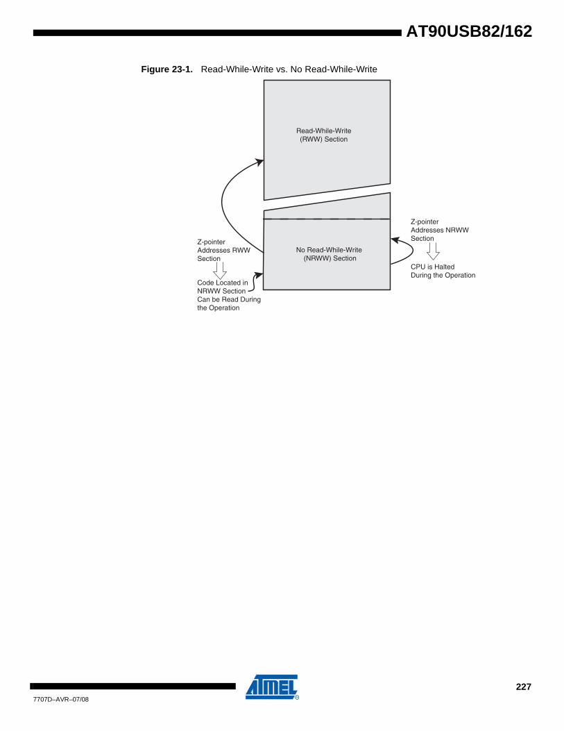
AT90USB82/162
Figure 23-1. Read-While-Write vs. No Read-While-Write
Read-While-Write(RWW) Section
No Read-While-Write (NRWW) Section
Z-pointerAddresses RWWSection
Z-pointerAddresses NRWWSection
CPU is HaltedDuring the Operation
Code Located in NRWW SectionCan be Read Duringthe Operation
2277707D–AVR–07/08

Figure 23-2. Memory Sections
Note: 1. The parameters in the figure above are given in Table 23-8 on page 239.
23.4 Boot Loader Lock BitsIf no Boot Loader capability is needed, the entire Flash is available for application code. The Boot Loader has two separate sets of Boot Lock bits which can be set independently. This gives the user a unique flexibility to select different levels of protection.
The user can select:
• To protect the entire Flash from a software update by the MCU.
• To protect only the Boot Loader Flash section from a software update by the MCU.
• To protect only the Application Flash section from a software update by the MCU.
• Allow software update in the entire Flash.
See Table 23-2 and Table 23-3 for further details. The Boot Lock bits can be set in software and in Serial or Parallel Programming mode, but they can be cleared by a Chip Erase command only. The general Write Lock (Lock Bit mode 2) does not control the programming of the Flash memory by SPM instruction. Similarly, the general Read/Write Lock (Lock Bit mode 1) does not control reading nor writing by (E)LPM/SPM, if it is attempted.
0x0000
Flashend
Program MemoryBOOTSZ = '11'
Application Flash Section
Boot Loader Flash SectionFlashend
Program MemoryBOOTSZ = '10'
0x0000
Program MemoryBOOTSZ = '01'
Program MemoryBOOTSZ = '00'
Application Flash Section
Boot Loader Flash Section
0x0000
Flashend
Application Flash Section
Flashend
End RWW
Start NRWW
Application Flash Section
Boot Loader Flash Section
Boot Loader Flash Section
End RWW
Start NRWW
End RWW
Start NRWW
0x0000
End RWW, End Application
Start NRWW, Start Boot Loader
Application Flash SectionApplication Flash Section
Application Flash Section
Rea
d-W
hile
-Writ
e S
ectio
nN
o R
ead-
Whi
le-W
rite
Sec
tion
Rea
d-W
hile
-Writ
e S
ectio
nN
o R
ead-
Whi
le-W
rite
Sec
tion
Rea
d-W
hile
-Writ
e S
ectio
nN
o R
ead-
Whi
le-W
rite
Sec
tion
Rea
d-W
hile
-Writ
e S
ectio
nN
o R
ead-
Whi
le-W
rite
Sec
tion
End Application
Start Boot Loader
End Application
Start Boot Loader
End Application
Start Boot Loader
2287707D–AVR–07/08
AT90USB82/162

AT90USB82/162
Note: 1. “1” means unprogrammed, “0” means programmed
Note: 1. “1” means unprogrammed, “0” means programmed
23.5 Entering the Boot Loader ProgramThe bootloader can be executed with three different conditions:
23.5.1 Regular application conditions.A jump or call from the application program. This may be initiated by a trigger such as a com-mand received via USART, or SPI interface.
23.5.2 Boot Reset FuseThe Boot Reset Fuse (BOOTRST) can be programmed so that the Reset Vector is pointing to the Boot Flash start address after a reset. In this case, the Boot Loader is started after a reset. After the application code is loaded, the program can start executing the application code. Note that the fuses cannot be changed by the MCU itself. This means that once the Boot Reset Fuse
Table 23-2. Boot Lock Bit0 Protection Modes (Application Section)(1)
BLB0 Mode BLB02 BLB01 Protection
1 1 1No restrictions for SPM or (E)LPM accessing the Application section.
2 1 0 SPM is not allowed to write to the Application section.
3 0 0
SPM is not allowed to write to the Application section, and (E)LPM executing from the Boot Loader section is not allowed to read from the Application section. If Interrupt Vectors are placed in the Boot Loader section, interrupts are disabled while executing from the Application section.
4 0 1
(E)LPM executing from the Boot Loader section is not allowed to read from the Application section. If Interrupt Vectors are placed in the Boot Loader section, interrupts are disabled while executing from the Application section.
Table 23-3. Boot Lock Bit1 Protection Modes (Boot Loader Section)(1)
BLB1 Mode BLB12 BLB11 Protection
1 1 1No restrictions for SPM or (E)LPM accessing the Boot Loader section.
2 1 0 SPM is not allowed to write to the Boot Loader section.
3 0 0
SPM is not allowed to write to the Boot Loader section, and (E)LPM executing from the Application section is not allowed to read from the Boot Loader section. If Interrupt Vectors are placed in the Application section, interrupts are disabled while executing from the Boot Loader section.
4 0 1
(E)LPM executing from the Application section is not allowed to read from the Boot Loader section. If Interrupt Vectors are placed in the Application section, interrupts are disabled while executing from the Boot Loader section.
2297707D–AVR–07/08

is programmed, the Reset Vector will always point to the Boot Loader Reset and the fuse can only be changed through the serial or parallel programming interface.
Note: 1. “1” means unprogrammed, “0” means programmed
23.5.3 External Hardware conditionsThe Hardware Boot Enable Fuse (HWBE) can be programmed (See Table 23-5) so that upon special hardware conditions under reset, the bootloader execution is forced after reset.
Note: 1. “1” means unprogrammed, “0” means programmed
When the HWBE fuse is enable the PD7/HWB pin is configured as input during reset and sam-pled during reset rising edge. When PD7/HWB pin is ‘0’ during reset rising edge, the reset vector will be set as the Boot Loader Reset address and the Boot Loader will be executed (See Figures 23-3).
Table 23-4. Boot Reset Fuse(1)
BOOTRST Reset Address
1 Reset Vector = Application Reset (address 0x0000)
0 Reset Vector = Boot Loader Reset (see Table 23-8 on page 239)
Table 23-5. Hardware Boot Enable Fuse(1)
HWBE Reset Address
1 PD7/HWB pin can not be used to force Boot Loader execution after reset
0 PD7/HWB pin is used during reset to force bootloader execution after reset
2307707D–AVR–07/08
AT90USB82/162

AT90USB82/162
Figure 23-3. Boot Process Description
23.5.4 Store Program Memory Control and Status Register – SPMCSRThe Store Program Memory Control and Status Register contains the control bits needed to con-trol the Boot Loader operations.
• Bit 7 – SPMIE: SPM Interrupt EnableWhen the SPMIE bit is written to one, and the I-bit in the Status Register is set (one), the SPM ready interrupt will be enabled. The SPM ready Interrupt will be executed as long as the SPMEN bit in the SPMCSR Register is cleared.
• Bit 6 – RWWSB: Read-While-Write Section BusyWhen a Self-Programming (Page Erase or Page Write) operation to the RWW section is initi-ated, the RWWSB will be set (one) by hardware. When the RWWSB bit is set, the RWW section cannot be accessed. The RWWSB bit will be cleared if the RWWSRE bit is written to one after a Self-Programming operation is completed. Alternatively the RWWSB bit will automatically be cleared if a page load operation is initiated.
• Bit 5 – SIGRD: Signature Row ReadIf this bit is written to one at the same time as SPMEN, the next LPM instruction within three clock cycles will read a byte from the signature row into the destination register. see “Reading the Signature Row from Software” on page 236 for details. An SPM instruction within four cycles
HWBE
BOOTRST ?
Ext. Hardware
Conditions ?
Reset Vector = Application Reset Reset Vector =Boot Lhoader Reset
?
RESET
PD7/HWB
tSHRH tHHRH
Bit 7 6 5 4 3 2 1 0
SPMIE RWWSB SIGRD RWWSRE BLBSET PGWRT PGERS SPMEN SPMCSR
Read/Write R/W R R/W R/W R/W R/W R/W R/W
Initial Value 0 0 0 0 0 0 0 0
2317707D–AVR–07/08

after SIGRD and SPMEN are set will have no effect. This operation is reserved for future use and should not be used.
• Bit 4 – RWWSRE: Read-While-Write Section Read EnableWhen programming (Page Erase or Page Write) to the RWW section, the RWW section is blocked for reading (the RWWSB will be set by hardware). To re-enable the RWW section, the user software must wait until the programming is completed (SPMEN will be cleared). Then, if the RWWSRE bit is written to one at the same time as SPMEN, the next SPM instruction within four clock cycles re-enables the RWW section. The RWW section cannot be re-enabled while the Flash is busy with a Page Erase or a Page Write (SPMEN is set). If the RWWSRE bit is writ-ten while the Flash is being loaded, the Flash load operation will abort and the data loaded will be lost.
• Bit 3 – BLBSET: Boot Lock Bit SetIf this bit is written to one at the same time as SPMEN, the next SPM instruction within four clock cycles sets Boot Lock bits, according to the data in R0. The data in R1 and the address in the Z-pointer are ignored. The BLBSET bit will automatically be cleared upon completion of the Lock bit set, or if no SPM instruction is executed within four clock cycles.
An (E)LPM instruction within three cycles after BLBSET and SPMEN are set in the SPMCSR Register, will read either the Lock bits or the Fuse bits (depending on Z0 in the Z-pointer) into the destination register. See “Reading the Fuse and Lock Bits from Software” on page 235 for details.
• Bit 2 – PGWRT: Page WriteIf this bit is written to one at the same time as SPMEN, the next SPM instruction within four clock cycles executes Page Write, with the data stored in the temporary buffer. The page address is taken from the high part of the Z-pointer. The data in R1 and R0 are ignored. The PGWRT bit will auto-clear upon completion of a Page Write, or if no SPM instruction is executed within four clock cycles. The CPU is halted during the entire Page Write operation if the NRWW section is addressed.
• Bit 1 – PGERS: Page EraseIf this bit is written to one at the same time as SPMEN, the next SPM instruction within four clock cycles executes Page Erase. The page address is taken from the high part of the Z-pointer. The data in R1 and R0 are ignored. The PGERS bit will auto-clear upon completion of a Page Erase, or if no SPM instruction is executed within four clock cycles. The CPU is halted during the entire Page Write operation if the NRWW section is addressed.
• Bit 0 – SPMEN: Store Program Memory EnableThis bit enables the SPM instruction for the next four clock cycles. If written to one together with either RWWSRE, BLBSET, PGWRT’ or PGERS, the following SPM instruction will have a spe-cial meaning, see description above. If only SPMEN is written, the following SPM instruction will store the value in R1:R0 in the temporary page buffer addressed by the Z-pointer. The LSB of the Z-pointer is ignored. The SPMEN bit will auto-clear upon completion of an SPM instruction, or if no SPM instruction is executed within four clock cycles. During Page Erase and Page Write, the SPMEN bit remains high until the operation is completed.
Writing any other combination than “10001”, “01001”, “00101”, “00011” or “00001” in the lower five bits will have no effect.
2327707D–AVR–07/08
AT90USB82/162

AT90USB82/162
Note: Only one SPM instruction should be active at any time.
23.6 Addressing the Flash During Self-ProgrammingThe Z-pointer is used to address the SPM commands. The Z pointer consists of the Z-registers ZL and ZH in the register file. The number of bits actually used is implementation dependent.
Since the Flash is organized in pages (see Table 25-11 on page 248), the Program Counter can be treated as having two different sections. One section, consisting of the least significant bits, is addressing the words within a page, while the most significant bits are addressing the pages. This is shown in Figure 23-4. Note that the Page Erase and Page Write operations are addressed independently. Therefore it is of major importance that the Boot Loader software addresses the same page in both the Page Erase and Page Write operation. Once a program-ming operation is initiated, the address is latched and the Z-pointer can be used for other operations.
The (E)LPM instruction use the Z-pointer to store the address. Since this instruction addresses the Flash byte-by-byte, also bit Z0 of the Z-pointer is used.
Figure 23-4. Addressing the Flash During SPM(1)
Note: 1. The different variables used in Figure 23-4 are listed in Table 23-10 on page 240.
23.7 Self-Programming the FlashThe program memory is updated in a page by page fashion. Before programming a page with the data stored in the temporary page buffer, the page must be erased. The temporary page buffer is filled one word at a time using SPM and the buffer can be filled either before the Page Erase command or between a Page Erase and a Page Write operation:
Alternative 1, fill the buffer before a Page Erase
• Fill temporary page buffer
PROGRAM MEMORY
0115
Z - REGISTER
BIT
0
ZPAGEMSB
WORD ADDRESSWITHIN A PAGE
PAGE ADDRESSWITHIN THE FLASH
ZPCMSB
INSTRUCTION WORD
PAGE PCWORD[PAGEMSB:0]:
00
01
02
PAGEEND
PAGE
PCWORDPCPAGE
PCMSB PAGEMSBPROGRAMCOUNTER
2337707D–AVR–07/08

• Perform a Page Erase
• Perform a Page Write
Alternative 2, fill the buffer after Page Erase
• Perform a Page Erase
• Fill temporary page buffer
• Perform a Page Write
If only a part of the page needs to be changed, the rest of the page must be stored (for example in the temporary page buffer) before the erase, and then be rewritten. When using alternative 1, the Boot Loader provides an effective Read-Modify-Write feature which allows the user software to first read the page, do the necessary changes, and then write back the modified data. If alter-native 2 is used, it is not possible to read the old data while loading since the page is already erased. The temporary page buffer can be accessed in a random sequence. It is essential that the page address used in both the Page Erase and Page Write operation is addressing the same page. See “Simple Assembly Code Example for a Boot Loader” on page 237 for an assembly code example.
23.7.1 Performing Page Erase by SPMTo execute Page Erase, set up the address in the Z-pointer, write “X0000011” to SPMCSR and execute SPM within four clock cycles after writing SPMCSR. The data in R1 and R0 is ignored. The page address must be written to PCPAGE in the Z-register. Other bits in the Z-pointer will be ignored during this operation.
• Page Erase to the RWW section: The NRWW section can be read during the Page Erase.
• Page Erase to the NRWW section: The CPU is halted during the operation.
23.7.2 Filling the Temporary Buffer (Page Loading)To write an instruction word, set up the address in the Z-pointer and data in R1:R0, write “00000001” to SPMCSR and execute SPM within four clock cycles after writing SPMCSR. The content of PCWORD in the Z-register is used to address the data in the temporary buffer. The temporary buffer will auto-erase after a Page Write operation or by writing the RWWSRE bit in SPMCSR. It is also erased after a system reset. Note that it is not possible to write more than one time to each address without erasing the temporary buffer.
If the EEPROM is written in the middle of an SPM Page Load operation, all data loaded will be lost.
23.7.3 Performing a Page WriteTo execute Page Write, set up the address in the Z-pointer, write “X0000101” to SPMCSR and execute SPM within four clock cycles after writing SPMCSR. The data in R1 and R0 is ignored. The page address must be written to PCPAGE. Other bits in the Z-pointer must be written to zero during this operation.
• Page Write to the RWW section: The NRWW section can be read during the Page Write.
• Page Write to the NRWW section: The CPU is halted during the operation.
23.7.4 Using the SPM InterruptIf the SPM interrupt is enabled, the SPM interrupt will generate a constant interrupt when the SPMEN bit in SPMCSR is cleared. This means that the interrupt can be used instead of polling the SPMCSR Register in software. When using the SPM interrupt, the Interrupt Vectors should
2347707D–AVR–07/08
AT90USB82/162

AT90USB82/162
be moved to the BLS section to avoid that an interrupt is accessing the RWW section when it is blocked for reading. How to move the interrupts is described in “Interrupts” on page 63.
23.7.5 Consideration While Updating BLSSpecial care must be taken if the user allows the Boot Loader section to be updated by leaving Boot Lock bit11 unprogrammed. An accidental write to the Boot Loader itself can corrupt the entire Boot Loader, and further software updates might be impossible. If it is not necessary to change the Boot Loader software itself, it is recommended to program the Boot Lock bit11 to protect the Boot Loader software from any internal software changes.
23.7.6 Prevent Reading the RWW Section During Self-ProgrammingDuring Self-Programming (either Page Erase or Page Write), the RWW section is always blocked for reading. The user software itself must prevent that this section is addressed during the self programming operation. The RWWSB in the SPMCSR will be set as long as the RWW section is busy. During Self-Programming the Interrupt Vector table should be moved to the BLS as described in “Interrupts” on page 63, or the interrupts must be disabled. Before addressing the RWW section after the programming is completed, the user software must clear the RWWSB by writing the RWWSRE. See “Simple Assembly Code Example for a Boot Loader” on page 237 for an example.
23.7.7 Setting the Boot Loader Lock Bits by SPMTo set the Boot Loader Lock bits, write the desired data to R0, write “X0001001” to SPMCSR and execute SPM within four clock cycles after writing SPMCSR. The only accessible Lock bits are the Boot Lock bits that may prevent the Application and Boot Loader section from any soft-ware update by the MCU.
See Table 23-2 and Table 23-3 for how the different settings of the Boot Loader bits affect the Flash access.
If bits 5..2 in R0 are cleared (zero), the corresponding Boot Lock bit will be programmed if an SPM instruction is executed within four cycles after BLBSET and SPMEN are set in SPMCSR. The Z-pointer is don’t care during this operation, but for future compatibility it is recommended to load the Z-pointer with 0x0001 (same as used for reading the lOck bits). For future compatibility it is also recommended to set bits 7, 6, 1, and 0 in R0 to “1” when writing the Lock bits. When pro-gramming the Lock bits the entire Flash can be read during the operation.
23.7.8 EEPROM Write Prevents Writing to SPMCSRNote that an EEPROM write operation will block all software programming to Flash. Reading the Fuses and Lock bits from software will also be prevented during the EEPROM write operation. It is recommended that the user checks the status bit (EEPE) in the EECR Register and verifies that the bit is cleared before writing to the SPMCSR Register.
23.7.9 Reading the Fuse and Lock Bits from SoftwareIt is possible to read both the Fuse and Lock bits from software. To read the Lock bits, load the Z-pointer with 0x0001 and set the BLBSET and SPMEN bits in SPMCSR. When an (E)LPM instruction is executed within three CPU cycles after the BLBSET and SPMEN bits are set in SPMCSR, the value of the Lock bits will be loaded in the destination register. The BLBSET and SPMEN bits will auto-clear upon completion of reading the Lock bits or if no (E)LPM instruction
Bit 7 6 5 4 3 2 1 0
R0 1 1 BLB12 BLB11 BLB02 BLB01 1 1
2357707D–AVR–07/08

is executed within three CPU cycles or no SPM instruction is executed within four CPU cycles. When BLBSET and SPMEN are cleared, (E)LPM will work as described in the Instruction set Manual.
The algorithm for reading the Fuse Low byte is similar to the one described above for reading the Lock bits. To read the Fuse Low byte, load the Z-pointer with 0x0000 and set the BLBSET and SPMEN bits in SPMCSR. When an (E)LPM instruction is executed within three cycles after the BLBSET and SPMEN bits are set in the SPMCSR, the value of the Fuse Low byte (FLB) will be loaded in the destination register as shown below. Refer to Table 25-5 on page 245 for a detailed description and mapping of the Fuse Low byte.
Similarly, when reading the Fuse High byte, load 0x0003 in the Z-pointer. When an (E)LPM instruction is executed within three cycles after the BLBSET and SPMEN bits are set in the SPMCSR, the value of the Fuse High byte (FHB) will be loaded in the destination register as shown below. Refer to Table 25-4 on page 245 for detailed description and mapping of the Fuse High byte.
When reading the Extended Fuse byte, load 0x0002 in the Z-pointer. When an (E)LPM instruc-tion is executed within three cycles after the BLBSET and SPMEN bits are set in the SPMCSR, the value of the Extended Fuse byte (EFB) will be loaded in the destination register as shown below. Refer to Table 25-3 on page 244 for detailed description and mapping of the Extended Fuse byte.
Fuse and Lock bits that are programmed, will be read as zero. Fuse and Lock bits that are unprogrammed, will be read as one.
23.7.10 Reading the Signature Row from SoftwareTo read the Signature Row from software, load the Z-pointer with the signature byte address given in Table 23-6 on page 236 and set the SIGRD and SPMEN bits in SPMCSR. When an LPM instruction is executed within three CPU cycles after the SIGRD and SPMEN bits are set in SPMCSR, the signature byte value will be loaded in the destination register. The SIGRD and SPMEN bits will auto-clear upon completion of reading the Signature Row Lock bits or if no LPM instruction is executed within three CPU cycles. When SIGRD and SPMEN are cleared, LPM will work as described in the Instruction set Manual.
Bit 7 6 5 4 3 2 1 0
Rd – – BLB12 BLB11 BLB02 BLB01 LB2 LB1
Bit 7 6 5 4 3 2 1 0
Rd FLB7 FLB6 FLB5 FLB4 FLB3 FLB2 FLB1 FLB0
Bit 7 6 5 4 3 2 1 0
Rd FHB7 FHB6 FHB5 FHB4 FHB3 FHB2 FHB1 FHB0
Bit 7 6 5 4 3 2 1 0
Rd – – – – – EFB2 EFB1 EFB0
Table 23-6. Signature Row Addressing
Signature Byte Z-Pointer Address
Device Signature Byte 1 0x0000
Device Signature Byte 2 0x0002
Device Signature Byte 3 0x0004
RC Oscillator Calibration Byte 0x0001
2367707D–AVR–07/08
AT90USB82/162

AT90USB82/162
Note: All other addresses are reserved for future use.
23.7.11 Preventing Flash CorruptionDuring periods of low VCC, the Flash program can be corrupted because the supply voltage is too low for the CPU and the Flash to operate properly. These issues are the same as for board level systems using the Flash, and the same design solutions should be applied.
A Flash program corruption can be caused by two situations when the voltage is too low. First, a regular write sequence to the Flash requires a minimum voltage to operate correctly. Secondly, the CPU itself can execute instructions incorrectly, if the supply voltage for executing instructions is too low.
Flash corruption can easily be avoided by following these design recommendations (one is sufficient):
1. If there is no need for a Boot Loader update in the system, program the Boot Loader Lock bits to prevent any Boot Loader software updates.
2. Keep the AVR RESET active (low) during periods of insufficient power supply voltage. This can be done by enabling the internal Brown-out Detector (BOD) if the operating voltage matches the detection level. If not, an external low VCC reset protection circuit can be used. If a reset occurs while a write operation is in progress, the write operation will be completed provided that the power supply voltage is sufficient.
3. Keep the AVR core in Power-down sleep mode during periods of low VCC. This will pre-vent the CPU from attempting to decode and execute instructions, effectively protecting the SPMCSR Register and thus the Flash from unintentional writes.
23.7.12 Programming Time for Flash when Using SPMThe calibrated RC Oscillator is used to time Flash accesses. Table 23-7 shows the typical pro-gramming time for Flash accesses from the CPU.
23.7.13 Simple Assembly Code Example for a Boot Loader;-the routine writes one page of data from RAM to Flash ; the first data location in RAM is pointed to by the Y pointer ; the first data location in Flash is pointed to by the Z-pointer ;-error handling is not included ;-the routine must be placed inside the Boot space ; (at least the Do_spm sub routine). Only code inside NRWW section can ; be read during Self-Programming (Page Erase and Page Write). ;-registers used: r0, r1, temp1 (r16), temp2 (r17), looplo (r24), ; loophi (r25), spmcrval (r20) ; storing and restoring of registers is not included in the routine ; register usage can be optimized at the expense of code size ;-It is assumed that either the interrupt table is moved to the Boot ; loader section or that the interrupts are disabled.
.equ PAGESIZEB = PAGESIZE*2 ;PAGESIZEB is page size in BYTES, not words
.org SMALLBOOTSTART Write_page: ; Page Erase ldi spmcrval, (1<<PGERS) | (1<<SPMEN)
Table 23-7. SPM Programming Time
Symbol Min Programming Time Max Programming Time
Flash write (Page Erase, Page Write, and write Lock bits by SPM)
3.7 ms 4.5 ms
2377707D–AVR–07/08

call Do_spm ; re-enable the RWW section ldi spmcrval, (1<<RWWSRE) | (1<<SPMEN) call Do_spm ; transfer data from RAM to Flash page buffer ldi looplo, low(PAGESIZEB) ;init loop variable ldi loophi, high(PAGESIZEB) ;not required for PAGESIZEB<=256
Wrloop: ld r0, Y+ ld r1, Y+ ldi spmcrval, (1<<SPMEN) call Do_spm adiw ZH:ZL, 2 sbiw loophi:looplo, 2 ;use subi for PAGESIZEB<=256 brne Wrloop
; execute Page Write subi ZL, low(PAGESIZEB) ;restore pointer sbci ZH, high(PAGESIZEB) ;not required for PAGESIZEB<=256 ldi spmcrval, (1<<PGWRT) | (1<<SPMEN) call Do_spm
; re-enable the RWW section ldi spmcrval, (1<<RWWSRE) | (1<<SPMEN) call Do_spm
; read back and check, optional ldi looplo, low(PAGESIZEB) ;init loop variable ldi loophi, high(PAGESIZEB) ;not required for PAGESIZEB<=256 subi YL, low(PAGESIZEB) ;restore pointer sbci YH, high(PAGESIZEB)
Rdloop: elpm r0, Z+ ld r1, Y+ cpse r0, r1 jmp Error sbiw loophi:looplo, 1 ;use subi for PAGESIZEB<=256 brne Rdloop
; return to RWW section ; verify that RWW section is safe to read
Return: in temp1, SPMCSR sbrs temp1, RWWSB ; If RWWSB is set, the RWW section is not ready yet ret ; re-enable the RWW section ldi spmcrval, (1<<RWWSRE) | (1<<SPMEN) call Do_spm rjmp Return
Do_spm: ; check for previous SPM complete
Wait_spm: in temp1, SPMCSR sbrc temp1, SPMEN rjmp Wait_spm ; input: spmcrval determines SPM action
2387707D–AVR–07/08
AT90USB82/162
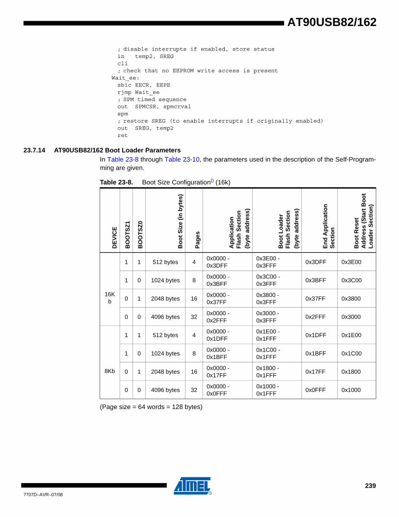
AT90USB82/162
; disable interrupts if enabled, store status in temp2, SREG cli ; check that no EEPROM write access is present
Wait_ee: sbic EECR, EEPE rjmp Wait_ee ; SPM timed sequence out SPMCSR, spmcrval spm ; restore SREG (to enable interrupts if originally enabled) out SREG, temp2 ret
23.7.14 AT90USB82/162 Boot Loader ParametersIn Table 23-8 through Table 23-10, the parameters used in the description of the Self-Program-ming are given.
(Page size = 64 words = 128 bytes)
Table 23-8. Boot Size Configuration() (16k)
DE
VIC
E
BO
OT
SZ
1
BO
OT
SZ
0
Bo
ot
Siz
e (i
n b
ytes
)
Pag
es
Ap
plic
atio
n
Fla
sh S
ecti
on
(byt
e ad
dre
ss)
Bo
ot
Lo
ader
F
lash
Sec
tio
n(b
yte
add
ress
)
En
d A
pp
licat
ion
S
ecti
on
Bo
ot
Res
et
Ad
dre
ss (
Sta
rt B
oo
t
Lo
ader
Sec
tio
n)
16Kb
1 1 512 bytes 40x0000 - 0x3DFF
0x3E00 - 0x3FFF
0x3DFF 0x3E00
1 0 1024 bytes 80x0000 - 0x3BFF
0x3C00 - 0x3FFF
0x3BFF 0x3C00
0 1 2048 bytes 160x0000 - 0x37FF
0x3800 - 0x3FFF
0x37FF 0x3800
0 0 4096 bytes 320x0000 - 0x2FFF
0x3000 - 0x3FFF
0x2FFF 0x3000
8Kb
1 1 512 bytes 40x0000 - 0x1DFF
0x1E00 - 0x1FFF
0x1DFF 0x1E00
1 0 1024 bytes 80x0000 - 0x1BFF
0x1C00 - 0x1FFF
0x1BFF 0x1C00
0 1 2048 bytes 160x0000 - 0x17FF
0x1800 - 0x1FFF
0x17FF 0x1800
0 0 4096 bytes 320x0000 - 0x0FFF
0x1000 - 0x1FFF
0x0FFF 0x1000
2397707D–AVR–07/08

The different BOOTSZ Fuse configurations are shown in Figure 23-2.
Note: 1. For details about these two section, see “NRWW – No Read-While-Write Section” on page 226 and “RWW – Read-While-Write Section” on page 226.
Note: 1. Z0: should be zero for all SPM commands, byte select for the (E)LPM instruction.
See “Addressing the Flash During Self-Programming” on page 233 for details about the use of Z-pointer during Self-Programming.
Table 23-9. Read-While-Write Limit(1)
Device Section Pages Address
16KRead-While-Write section (RWW) 96 0x0000 - 0x2FFF
No Read-While-Write section (NRWW) 32 0x3000 - 0x3FFF
8KRead-While-Write section (RWW) 32 0x0000 - 0x0FFF
No Read-While-Write section (NRWW) 32 0x1000 - 0x1FFF
Table 23-10. Explanation of different variables used in Figure 23-4 and the mapping to the Z-pointer
VariableCorresponding
Z-value Description(1)
PCMSB 12Most significant bit in the Program Counter. (The Program Counter is 13 bits PC[12:0])
PAGEMSB 5Most significant bit which is used to address the words within one page (64 words in a page requires six bits PC [5:0]).
ZPCMSB Z13Bit in Z-pointer that is mapped to PCMSB. Because Z0 is not used, the ZPCMSB equals PCMSB + 1.
ZPAGEMSB Z6Bit in Z-pointer that is mapped to PCMSB. Because Z0 is not used, the ZPAGEMSB equals PAGEMSB + 1.
PCPAGE PC[12:6] Z13:Z7Program Counter page address: Page select, for Page Erase and Page Write
PCWORD PC[5:0] Z6:Z1Program Counter word address: Word select, for filling temporary buffer (must be zero during Page Write operation)
2407707D–AVR–07/08
AT90USB82/162

AT90USB82/162
24. debugWIRE On-chip Debug System
24.1 Features• Complete Program Flow Control• Emulates All On-chip Functions, Both Digital and Analog, except RESET Pin• Real-time Operation• Symbolic Debugging Support (Both at C and Assembler Source Level, or for Other HLLs)• Unlimited Number of Program Break Points (Using Software Break Points)• Non-intrusive Operation• Electrical Characteristics Identical to Real Device• Automatic Configuration System• High-Speed Operation• Programming of Non-volatile Memories
24.2 OverviewThe debugWIRE On-chip debug system uses a One-wire, bi-directional interface to control the program flow, execute AVR instructions in the CPU and to program the different non-volatile memories.
24.3 Physical InterfaceWhen the debugWIRE Enable (DWEN) Fuse is programmed and Lock bits are unprogrammed, the debugWIRE system within the target device is activated. The RESET port pin is configured as a wire-AND (open-drain) bi-directional I/O pin and becomes the communication gateway between target and emulator.
Figure 24-1. The debugWIRE Setup
Figure 24-1 shows the schematic of a target MCU, with debugWIRE enabled, and the emulator connector. The system clock is not affected by debugWIRE and will always be the clock source selected by the CKSEL Fuses.
dW
GND
dW(RESET)
VCC
2.7 - 5.5
(See
Not
e)
2417707D–AVR–07/08

When designing a system where debugWIRE will be used, the following observations must be made for correct operation:
• Connecting the RESET pin directly to VCC will not work.
• Any capacitors (or additionnal circuitry) connected to the RESET pin must be disconnected when using debugWire.
• All external reset sources must be disconnected.
Note: some releases of JTAG Ice mkII firmware may require a pull-up resistor with a value between 8 and 14 kOhms when operating at 5V.
24.4 Software Break PointsdebugWIRE supports Program memory Break Points by the AVR Break instruction. Setting a Break Point in AVR Studio® will insert a BREAK instruction in the Program memory. The instruc-tion replaced by the BREAK instruction will be stored. When program execution is continued, the stored instruction will be executed before continuing from the Program memory. A break can be inserted manually by putting the BREAK instruction in the program.
The Flash must be re-programmed each time a Break Point is changed. This is automatically handled by AVR Studio through the debugWIRE interface. The use of Break Points will therefore reduce the Flash Data retention. Devices used for debugging purposes should not be shipped to end customers.
24.5 Limitations of debugWIREThe debugWIRE communication pin (dW) is physically located on the same pin as External Reset (RESET). An External Reset source is therefore not supported when the debugWIRE is enabled.
The debugWIRE system accurately emulates all I/O functions when running at full speed, i.e., when the program in the CPU is running. When the CPU is stopped, care must be taken while accessing some of the I/O Registers via the debugger (AVR Studio).
A programmed DWEN Fuse enables some parts of the clock system to be running in all sleep modes. This will increase the power consumption while in sleep. Thus, the DWEN Fuse should be disabled when debugWire is not used.
24.6 debugWIRE Related Register in I/O Memory The following section describes the registers used with the debugWire.
24.6.1 debugWire Data Register – DWDR
The DWDR Register provides a communication channel from the running program in the MCU to the debugger. This register is only accessible by the debugWIRE and can therefore not be used as a general purpose register in the normal operations.
Bit 7 6 5 4 3 2 1 0
DWDR[7:0] DWDR
Read/Write R/W R/W R/W R/W R/W R/W R/W R/W
Initial Value 0 0 0 0 0 0 0 0
2427707D–AVR–07/08
AT90USB82/162

AT90USB82/162
25. Memory Programming
25.1 Program And Data Memory Lock BitsThe AT90USB82/162 provides six Lock bits which can be left unprogrammed (“1”) or can be pro-grammed (“0”) to obtain the additional features listed in Table 25-2. The Lock bits can only be erased to “1” with the Chip Erase command.
Note: 1. “1” means unprogrammed, “0” means programmed
Table 25-1. Lock Bit Byte(1)
Lock Bit Byte Bit No Description Default Value
7 – 1 (unprogrammed)
6 – 1 (unprogrammed)
BLB12 5 Boot Lock bit 1 (unprogrammed)
BLB11 4 Boot Lock bit 0 (programmed)
BLB02 3 Boot Lock bit 1 (unprogrammed)
BLB01 2 Boot Lock bit 1 (unprogrammed)
LB2 1 Lock bit 0 (programmed)
LB1 0 Lock bit 0 (programmed)
Table 25-2. Lock Bit Protection Modes(1)(2)
Memory Lock Bits Protection Type
LB Mode LB2 LB1
1 1 1 No memory lock features enabled.
2 1 0Further programming of the Flash and EEPROM is disabled in Parallel and Serial Programming mode. The Fuse bits are locked in both Serial and Parallel Programming mode.(1)
3 0 0
Further programming and verification of the Flash and EEPROM is disabled in Parallel and Serial Programming mode. The Boot Lock bits and Fuse bits are locked in both Serial and Parallel Programming mode.(1)
BLB0 Mode BLB02 BLB01
1 1 1No restrictions for SPM or (E)LPM accessing the Application section.
2 1 0 SPM is not allowed to write to the Application section.
3 0 0
SPM is not allowed to write to the Application section, and (E)LPM executing from the Boot Loader section is not allowed to read from the Application section. If Interrupt Vectors are placed in the Boot Loader section, interrupts are disabled while executing from the Application section.
4 0 1
(E)LPM executing from the Boot Loader section is not allowed to read from the Application section. If Interrupt Vectors are placed in the Boot Loader section, interrupts are disabled while executing from the Application section.
2437707D–AVR–07/08

Notes: 1. Program the Fuse bits and Boot Lock bits before programming the LB1 and LB2.
2. “1” means unprogrammed, “0” means programmed
25.2 Fuse BitsThe AT90USB82/162 has four Fuse bytes. Table 25-3 - Table 25-5 describe briefly the function-ality of all the fuses and how they are mapped into the Fuse bytes. Note that the fuses are read as logical zero, “0”, if they are programmed.
Note: 1. See Table 9-2 on page 49 for BODLEVEL Fuse decoding.
BLB1 Mode BLB12 BLB11
1 1 1No restrictions for SPM or (E)LPM accessing the Boot Loader section.
2 1 0 SPM is not allowed to write to the Boot Loader section.
3 0 0
SPM is not allowed to write to the Boot Loader section, and (E)LPM executing from the Application section is not allowed to read from the Boot Loader section. If Interrupt Vectors are placed in the Application section, interrupts are disabled while executing from the Boot Loader section.
4 0 1
(E)LPM executing from the Application section is not allowed to read from the Boot Loader section. If Interrupt Vectors are placed in the Application section, interrupts are disabled while executing from the Boot Loader section.
Table 25-2. Lock Bit Protection Modes(1)(2) (Continued)
Memory Lock Bits Protection Type
Table 25-3. Extended Fuse Byte
Fuse Low Byte Bit No Description Default Value : 0xF4
– 7 – 1
– 6 – 1
– 5 – 1
– 4 – 1
HWBE 3 Hardware Boot Enable 0 (programmed)
BODLEVEL2(1) 2 Brown-out Detector trigger level 1 (unprogrammed)
BODLEVEL1(1) 1 Brown-out Detector trigger level 0 (programmed)
BODLEVEL0(1) 0 Brown-out Detector trigger level 0 (programmed)
2447707D–AVR–07/08
AT90USB82/162

AT90USB82/162
Note: 1. The SPIEN Fuse is not accessible in serial programming mode.
2. The default value of BOOTSZ1..0 results in maximum Boot Size. See Table 23-8 on page 239 for details.
3. See “Watchdog Timer Control Register - WDTCSR” on page 56 for details.
4. Never ship a product with the DWEN Fuse programmed regardless of the setting of Lock bits and RSTDSBL Fuse. A programmed DWEN Fuse enables some parts of the clock system to be running in all sleep modes. This may increase the power consumption.
Note: 1. The default value of SUT1..0 results in maximum start-up time for the default clock source. See Table 9-1 on page 47 for details.
2. The default setting of CKSEL3..0 results in external Oscillator. See Table 6-1 on page 29 for details.
3. The CKOUT Fuse allow the system clock to be output on PORTC7. See “Clock Output Buffer” on page 34 for details.
4. See “System Clock Prescaler” on page 34 for details.
The status of the Fuse bits is not affected by Chip Erase. Note that the Fuse bits are locked if Lock bit1 (LB1) is programmed. Program the Fuse bits before programming the Lock bits.
Table 25-4. Fuse High Byte
Fuse High Byte Bit No Description Default Value : 0xD9
DWEN(4) 7Enable debugWIRE (and disable Reset capability
1 (unprogrammed, debugWIRE disabled)
RSTDSBL 6Disable Reset (pin can be used as general purpose I/O)
1 (unprogrammed, Reset enabled)
SPIEN(1) 5Enable Serial Program and Data Downloading
0 (programmed, SPI prog. enabled)
WDTON(3) 4 Watchdog Timer always ON 1 (unprogrammed)(3)
EESAVE 3EEPROM memory is preserved through the Chip Erase
1 (unprogrammed, EEPROM not preserved)
BOOTSZ1 2Select Boot Size (see Table 25-6 for details)
0 (programmed)(2)
BOOTSZ0 1Select Boot Size (see Table 25-6 for details)
0 (programmed)(2)
BOOTRST 0Select Bootloader Address as Reset Vector
1 (unprogrammed, Reset vector @0x0000)
Table 25-5. Fuse Low Byte
Fuse Low Byte Bit No Description Default Value : 0x5E
CKDIV8(4) 7 Divide clock by 8 0 (programmed)
CKOUT(3) 6 Clock output 1 (unprogrammed)
SUT1 5 Select start-up time 0 (programmed)(1)
SUT0 4 Select start-up time 1 (unprogrammed)(1)
CKSEL3 3 Select Clock source 1 (unprogrammed)(2)
CKSEL2 2 Select Clock source 1 (unprogrammed)(2)
CKSEL1 1 Select Clock source 1 (unprogrammed)(2)
CKSEL0 0 Select Clock source 0 (programmed)(2)
2457707D–AVR–07/08

25.2.1 Latching of FusesThe fuse values are latched when the device enters programming mode and changes of the fuse values will have no effect until the part leaves Programming mode. This does not apply to the EESAVE Fuse which will take effect once it is programmed. The fuses are also latched on Power-up in Normal mode.
25.3 Signature BytesAll Atmel microcontrollers have a three-byte signature code which identifies the device. This code can be read in both serial and parallel mode, also when the device is locked. The three bytes reside in a separate address space.
AT90USB82/162 Signature Bytes:
1. 0x000: 0x1E (indicates manufactured by Atmel).
2. 0x001: 0x94 (indicates 16KB Flash memory).
3. 0x002: 0x82 (indicates AT90USB82/162 device).
25.4 Calibration ByteThe AT90USB82/162 has a byte calibration value for the internal RC Oscillator. This byte resides in the high byte of address 0x000 in the signature address space. During reset, this byte is automatically written into the OSCCAL Register to ensure correct frequency of the calibrated RC Oscillator.
25.5 Parallel Programming Parameters, Pin Mapping, and CommandsThis section describes how to parallel program and verify Flash Program memory, EEPROM Data memory, Memory Lock bits, and Fuse bits in the AT90USB82/162. Pulses are assumed to be at least 250 ns unless otherwise noted.
25.5.1 Signal NamesIn this section, some pins of the AT90USB82/162 are referenced by signal names describing their functionality during parallel programming, see Figure 25-1 and Table 25-6. Pins not described in the following table are referenced by pin names.
The XA1/XA0 pins determine the action executed when the XTAL1 pin is given a positive pulse. The bit coding is shown in Table 25-9.
When pulsing WR or OE, the command loaded determines the action executed. The different commands are shown in Table 25-10.
2467707D–AVR–07/08
AT90USB82/162

AT90USB82/162
Figure 25-1. Parallel Programming(1)
Note: 1. Unused Pins should be left floating.
Table 25-6. Pin Name Mapping
Signal Name in Programming Mode Pin Name I/O Function
RDY/BSY PD1 O0: Device is busy programming, 1: Device is ready for new command.
OE PD2 I Output Enable (Active low).
WR PD3 I Write Pulse (Active low).
BS1 PD4 I Byte Select 1.
XA0 PD5 I XTAL Action Bit 0
XA1 PD6 I XTAL Action Bit 1
PAGEL PD7 I Program Memory and EEPROM data Page Load.
BS2 PC6 I Byte Select 2.
DATA PB7-0 I/O Bi-directional Data bus (Output when OE is low).
Table 25-7. BS2 and BS1 Encoding
BS2 BS1Flash / EEPROM Address
Flash Data Loading / Reading
Fuse Programming
Reading Fuse and Lock Bits
0 0 Low Byte Low Byte Low Byte Fuse Low Byte
0 1 High Byte High Byte High Byte Lockbits
1 0Extended High Byte
Reserved Extended ByteExtended Fuse Byte
1 1 Reserved Reserved Reserved Fuse High Byte
VCC
+5V
GND
XTAL1
PD1
PD2
PD3
PD4
PD5
PD6
PB7:0 DATA
RESET
PD7
+12 V
BS1
XA0
XA1
OE
RDY/BSY
PAGEL
PC6
WR
BS2
AVCC
+5V
2477707D–AVR–07/08

Table 25-8. Pin Values Used to Enter Programming Mode
Pin Symbol Value
PAGEL Prog_enable[3] 0
XA1 Prog_enable[2] 0
XA0 Prog_enable[1] 0
BS1 Prog_enable[0] 0
Table 25-9. XA1 and XA0 Encoding
XA1 XA0 Action when XTAL1 is Pulsed
0 0Load Flash or EEPROM Address (High or low address byte determined by BS2 and BS1).
0 1 Load Data (High or Low data byte for Flash determined by BS1).
1 0 Load Command
1 1 No Action, Idle
Table 25-10. Command Byte Bit Encoding
Command Byte Command Executed
1000 0000 Chip Erase
0100 0000 Write Fuse bits
0010 0000 Write Lock bits
0001 0000 Write Flash
0001 0001 Write EEPROM
0000 1000 Read Signature Bytes and Calibration byte
0000 0100 Read Fuse and Lock bits
0000 0010 Read Flash
0000 0011 Read EEPROM
Table 25-11. No. of Words in a Page and No. of Pages in the Flash
Flash Size Page Size PCWORDNo. of Pages PCPAGE PCMSB
4/8K words (8/16Kbytes) 64 words PC[5:0] 128 PC[12:6] 12
Table 25-12. No. of Bytes in a Page and No. of Pages in the EEPROM
EEPROM Size Page Size PCWORDNo. of Pages PCPAGE EEAMSB
512 bytes 4 bytes EEA[1:0] 128 EEA[8:2] 8
2487707D–AVR–07/08
AT90USB82/162

AT90USB82/162
25.6 Parallel Programming
25.6.1 Enter Programming ModeThe following algorithm puts the device in parallel programming mode:
1. Apply 4.5 - 5.5V between VCC and GND.
2. Set RESET to “0” and toggle XTAL1 at least six times.
3. Set the Prog_enable pins listed in Table 25-8 on page 248 to “0000” and wait at least 100 ns.
4. Apply 11.5 - 12.5V to RESET. Any activity on Prog_enable pins within 100 ns after +12V has been applied to RESET, will cause the device to fail entering programming mode.
5. Wait at least 50 µs before sending a new command.
25.6.2 Considerations for Efficient ProgrammingThe loaded command and address are retained in the device during programming. For efficient programming, the following should be considered.
• The command needs only be loaded once when writing or reading multiple memory locations.
• Skip writing the data value 0xFF, that is the contents of the entire EEPROM (unless the EESAVE Fuse is programmed) and Flash after a Chip Erase.
• Address high byte needs only be loaded before programming or reading a new 256 word window in Flash or 256 byte EEPROM. This consideration also applies to Signature bytes reading.
25.6.3 Chip EraseThe Chip Erase will erase the Flash and EEPROM(1) memories plus Lock bits. The Lock bits are not reset until the program memory has been completely erased. The Fuse bits are not changed. A Chip Erase must be performed before the Flash and/or EEPROM are reprogrammed.
Note: 1. The EEPRPOM memory is preserved during Chip Erase if the EESAVE Fuse is programmed.
Load Command “Chip Erase”
1. Set XA1, XA0 to “10”. This enables command loading.
2. Set BS1 to “0”.
3. Set DATA to “1000 0000”. This is the command for Chip Erase.
4. Give XTAL1 a positive pulse. This loads the command.
5. Give WR a negative pulse. This starts the Chip Erase. RDY/BSY goes low.
6. Wait until RDY/BSY goes high before loading a new command.
25.6.4 Programming the FlashThe Flash is organized in pages, see Table 25-11 on page 248. When programming the Flash, the program data is latched into a page buffer. This allows one page of program data to be pro-grammed simultaneously. The following procedure describes how to program the entire Flash memory:
A. Load Command “Write Flash”
2497707D–AVR–07/08

1. Set XA1, XA0 to “10”. This enables command loading.
2. Set BS1 to “0”.
3. Set DATA to “0001 0000”. This is the command for Write Flash.
4. Give XTAL1 a positive pulse. This loads the command.
B. Load Address Low byte (Address bits 7..0)
1. Set XA1, XA0 to “00”. This enables address loading.
2. Set BS2, BS1 to “00”. This selects the address low byte.
3. Set DATA = Address low byte (0x00 - 0xFF).
4. Give XTAL1 a positive pulse. This loads the address low byte.
C. Load Data Low Byte
1. Set XA1, XA0 to “01”. This enables data loading.
2. Set DATA = Data low byte (0x00 - 0xFF).
3. Give XTAL1 a positive pulse. This loads the data byte.
D. Load Data High Byte
1. Set BS1 to “1”. This selects high data byte.
2. Set XA1, XA0 to “01”. This enables data loading.
3. Set DATA = Data high byte (0x00 - 0xFF).
4. Give XTAL1 a positive pulse. This loads the data byte.
E. Latch Data
1. Set BS1 to “1”. This selects high data byte.
2. Give PAGEL a positive pulse. This latches the data bytes. (See Figure 25-3 for signal waveforms)
F. Repeat B through E until the entire buffer is filled or until all data within the page is loaded.
While the lower bits in the address are mapped to words within the page, the higher bits address the pages within the FLASH. This is illustrated in Figure 25-2 on page 251. Note that if less than eight bits are required to address words in the page (pagesize < 256), the most significant bit(s) in the address low byte are used to address the page when performing a Page Write.
G. Load Address High byte (Address bits15..8)
1. Set XA1, XA0 to “00”. This enables address loading.
2. Set BS2, BS1 to “01”. This selects the address high byte.
3. Set DATA = Address high byte (0x00 - 0xFF).
4. Give XTAL1 a positive pulse. This loads the address high byte.
H. Load Address Extended High byte (Address bits 23..16)
1. Set XA1, XA0 to “00”. This enables address loading.
2. Set BS2, BS1 to “10”. This selects the address extended high byte.
3. Set DATA = Address extended high byte (0x00 - 0xFF).
4. Give XTAL1 a positive pulse. This loads the address high byte.
I. Program Page
1. Set BS2, BS1 to “00”
2. Give WR a negative pulse. This starts programming of the entire page of data. RDY/BSY goes low.
2507707D–AVR–07/08
AT90USB82/162

AT90USB82/162
3. Wait until RDY/BSY goes high (See Figure 25-3 for signal waveforms).
J. Repeat B through I until the entire Flash is programmed or until all data has been programmed.
K. End Page Programming
1. 1. Set XA1, XA0 to “10”. This enables command loading.
2. Set DATA to “0000 0000”. This is the command for No Operation.
3. Give XTAL1 a positive pulse. This loads the command, and the internal write signals are reset.
Figure 25-2. Addressing the Flash Which is Organized in Pages(1)
Note: 1. PCPAGE and PCWORD are listed in Table 25-11 on page 248.
Figure 25-3. Programming the Flash Waveforms(1)
Note: 1. “XX” is don’t care. The letters refer to the programming description above.
PROGRAM MEMORY
WORD ADDRESSWITHIN A PAGE
PAGE ADDRESSWITHIN THE FLASH
INSTRUCTION WORD
PAGE PCWORD[PAGEMSB:0]:
00
01
02
PAGEEND
PAGE
PCWORDPCPAGE
PCMSB PAGEMSBPROGRAMCOUNTER
RDY/BSY
WR
OE
RESET +12V
PAGEL
BS2
0x10 ADDR. LOW ADDR. HIGHDATADATA LOW DATA HIGH ADDR. LOW DATA LOW DATA HIGH
XA1
XA0
BS1
XTAL1
XX XX XX
A B C D E B C D E G
F
ADDR. EXT.H
H I
2517707D–AVR–07/08

25.6.5 Programming the EEPROMThe EEPROM is organized in pages, see Table 25-12 on page 248. When programming the EEPROM, the program data is latched into a page buffer. This allows one page of data to be programmed simultaneously. The programming algorithm for the EEPROM data memory is as follows (refer to “Programming the Flash” on page 249 for details on Command, Address and Data loading):
1. A: Load Command “0001 0001”.
2. G: Load Address High Byte (0x00 - 0xFF).
3. B: Load Address Low Byte (0x00 - 0xFF).
4. C: Load Data (0x00 - 0xFF).
5. E: Latch data (give PAGEL a positive pulse).
K: Repeat 3 through 5 until the entire buffer is filled.
L: Program EEPROM page
1. Set BS2, BS1 to “00”.
2. Give WR a negative pulse. This starts programming of the EEPROM page. RDY/BSY goes low.
3. Wait until to RDY/BSY goes high before programming the next page (See Figure 25-4 for signal waveforms).
Figure 25-4. Programming the EEPROM Waveforms
25.6.6 Reading the FlashThe algorithm for reading the Flash memory is as follows (refer to “Programming the Flash” on page 249 for details on Command and Address loading):
1. A: Load Command “0000 0010”.
2. H: Load Address Extended Byte (0x00- 0xFF).
3. G: Load Address High Byte (0x00 - 0xFF).
4. B: Load Address Low Byte (0x00 - 0xFF).
5. Set OE to “0”, and BS1 to “0”. The Flash word low byte can now be read at DATA.
6. Set BS to “1”. The Flash word high byte can now be read at DATA.
7. Set OE to “1”.
RDY/BSY
WR
OE
RESET +12V
PAGEL
BS2
0x11 ADDR. HIGHDATA
ADDR. LOW DATA ADDR. LOW DATA XX
XA1
XA0
BS1
XTAL1
XX
A G B C E B C E L
K
2527707D–AVR–07/08
AT90USB82/162

AT90USB82/162
25.6.7 Reading the EEPROMThe algorithm for reading the EEPROM memory is as follows (refer to “Programming the Flash” on page 249 for details on Command and Address loading):
1. A: Load Command “0000 0011”.
2. G: Load Address High Byte (0x00 - 0xFF).
3. B: Load Address Low Byte (0x00 - 0xFF).
4. Set OE to “0”, and BS1 to “0”. The EEPROM Data byte can now be read at DATA.
5. Set OE to “1”.
25.6.8 Programming the Fuse Low BitsThe algorithm for programming the Fuse Low bits is as follows (refer to “Programming the Flash” on page 249 for details on Command and Data loading):
1. A: Load Command “0100 0000”.
2. C: Load Data Low Byte. Bit n = “0” programs and bit n = “1” erases the Fuse bit.
3. Give WR a negative pulse and wait for RDY/BSY to go high.
25.6.9 Programming the Fuse High BitsThe algorithm for programming the Fuse High bits is as follows (refer to “Programming the Flash” on page 249 for details on Command and Data loading):
1. A: Load Command “0100 0000”.
2. C: Load Data Low Byte. Bit n = “0” programs and bit n = “1” erases the Fuse bit.
3. Set BS2, BS1 to “01”. This selects high data byte.
4. Give WR a negative pulse and wait for RDY/BSY to go high.
5. Set BS2, BS1 to “00”. This selects low data byte.
25.6.10 Programming the Extended Fuse BitsThe algorithm for programming the Extended Fuse bits is as follows (refer to “Programming the Flash” on page 249 for details on Command and Data loading):
1. 1. A: Load Command “0100 0000”.
2. 2. C: Load Data Low Byte. Bit n = “0” programs and bit n = “1” erases the Fuse bit.
3. 3. Set BS2, BS1 to “10”. This selects extended data byte.
4. 4. Give WR a negative pulse and wait for RDY/BSY to go high.
5. 5. Set BS2, BS1 to “00”. This selects low data byte.
2537707D–AVR–07/08

Figure 25-5. Programming the FUSES Waveforms
25.6.11 Programming the Lock BitsThe algorithm for programming the Lock bits is as follows (refer to “Programming the Flash” on page 249 for details on Command and Data loading):
1. A: Load Command “0010 0000”.
2. C: Load Data Low Byte. Bit n = “0” programs the Lock bit. If LB mode 3 is programmed (LB1 and LB2 is programmed), it is not possible to program the Boot Lock bits by any External Programming mode.
3. Give WR a negative pulse and wait for RDY/BSY to go high.
The Lock bits can only be cleared by executing Chip Erase.
25.6.12 Reading the Fuse and Lock BitsThe algorithm for reading the Fuse and Lock bits is as follows (refer to “Programming the Flash” on page 249 for details on Command loading):
1. A: Load Command “0000 0100”.
2. Set OE to “0”, and BS2, BS1 to “00”. The status of the Fuse Low bits can now be read at DATA (“0” means programmed).
3. Set OE to “0”, and BS2, BS1 to “11”. The status of the Fuse High bits can now be read at DATA (“0” means programmed).
4. Set OE to “0”, and BS2, BS1 to “10”. The status of the Extended Fuse bits can now be read at DATA (“0” means programmed).
5. Set OE to “0”, and BS2, BS1 to “01”. The status of the Lock bits can now be read at DATA (“0” means programmed).
6. Set OE to “1”.
RDY/BSY
WR
OE
RESET +12V
PAGEL
0x40DATA
DATA XX
XA1
XA0
BS1
XTAL1
A C
0x40 DATA XX
A C
Write Fuse Low byte Write Fuse high byte
0x40 DATA XX
A C
Write Extended Fuse byte
BS2
2547707D–AVR–07/08
AT90USB82/162

AT90USB82/162
Figure 25-6. Mapping Between BS1, BS2 and the Fuse and Lock Bits During Read
25.6.13 Reading the Signature BytesThe algorithm for reading the Signature bytes is as follows (refer to “Programming the Flash” on page 249 for details on Command and Address loading):
1. A: Load Command “0000 1000”.
2. B: Load Address Low Byte (0x00 - 0x02).
3. Set OE to “0”, and BS to “0”. The selected Signature byte can now be read at DATA.
4. Set OE to “1”.
25.6.14 Reading the Calibration ByteThe algorithm for reading the Calibration byte is as follows (refer to “Programming the Flash” on page 249 for details on Command and Address loading):
1. A: Load Command “0000 1000”.
2. B: Load Address Low Byte, 0x00.
3. Set OE to “0”, and BS1 to “1”. The Calibration byte can now be read at DATA.
4. Set OE to “1”.
25.6.15 Parallel Programming Characteristics
Figure 25-7. Parallel Programming Timing, Including some General Timing Requirements
Lock Bits 0
1
BS2
Fuse High Byte
0
1
BS1
DATA
Fuse Low Byte 0
1
BS2
Extended Fuse Byte
Data & Contol(DATA, XA0/1, BS1, BS2)
XTAL1tXHXL
tWLWH
tDVXH tXLDX
tPLWL
tWLRH
WR
RDY/BSY
PAGEL tPHPL
tPLBXtBVPH
tXLWL
tWLBXtBVWL
WLRL
2557707D–AVR–07/08

Figure 25-8. Parallel Programming Timing, Loading Sequence with Timing Requirements(1)
Note: 1. The timing requirements shown in Figure 25-7 (i.e., tDVXH, tXHXL, and tXLDX) also apply to load-ing operation.
Figure 25-9. Parallel Programming Timing, Reading Sequence (within the Same Page) with Timing Requirements(1)
Note: 1. The timing requirements shown in Figure 25-7 (i.e., tDVXH, tXHXL, and tXLDX) also apply to read-ing operation.
Table 25-13. Parallel Programming Characteristics, VCC = 5V ± 10%
Symbol Parameter Min Typ Max Units
VPP Programming Enable Voltage 11.5 12.5 V
IPP Programming Enable Current 250 μA
tDVXH Data and Control Valid before XTAL1 High 67 ns
tXLXH XTAL1 Low to XTAL1 High 200 ns
tXHXL XTAL1 Pulse Width High 150 ns
tXLDX Data and Control Hold after XTAL1 Low 67 ns
XTAL1
PAGEL
tPLXHXLXHt tXLPH
ADDR0 (Low Byte) DATA (Low Byte) DATA (High Byte) ADDR1 (Low Byte)DATA
BS1
XA0
XA1
LOAD ADDRESS(LOW BYTE)
LOAD DATA (LOW BYTE)
LOAD DATA(HIGH BYTE)
LOAD DATA LOAD ADDRESS(LOW BYTE)
XTAL1
OE
ADDR0 (Low Byte) DATA (Low Byte) DATA (High Byte) ADDR1 (Low Byte)DATA
BS1
XA0
XA1
LOAD ADDRESS(LOW BYTE)
READ DATA (LOW BYTE)
READ DATA(HIGH BYTE)
LOAD ADDRESS(LOW BYTE)
tBVDV
tOLDV
tXLOL
tOHDZ
2567707D–AVR–07/08
AT90USB82/162

AT90USB82/162
Notes: 1. tWLRH is valid for the Write Flash, Write EEPROM, Write Fuse bits and Write Lock bits commands.
2. tWLRH_CE is valid for the Chip Erase command.
25.7 Serial DownloadingBoth the Flash and EEPROM memory arrays can be programmed using a serial programming bus while RESET is pulled to GND. The serial programming interface consists of pins SCK, PDI (input) and PDO (output). After RESET is set low, the Programming Enable instruction needs to be executed first before program/erase operations can be executed. NOTE, in Table 25-14 on page 257, the pin mapping for serial programming is listed. Not all packages use the SPI pins dedicated for the internal Serial Peripheral Interface - SPI.
25.8 Serial Programming Pin Mapping
Figure 25-10. Serial Programming and Verify(1)
tXLWL XTAL1 Low to WR Low 0 ns
tXLPH XTAL1 Low to PAGEL high 0 ns
tPLXH PAGEL low to XTAL1 high 150 ns
tBVPH BS1 Valid before PAGEL High 67 ns
tPHPL PAGEL Pulse Width High 150 ns
tPLBX BS1 Hold after PAGEL Low 67 ns
tWLBX BS2/1 Hold after WR Low 67 ns
tPLWL PAGEL Low to WR Low 67 ns
tBVWL BS2/1 Valid to WR Low 67 ns
tWLWH WR Pulse Width Low 150 ns
tWLRL WR Low to RDY/BSY Low 0 1 μs
tWLRH WR Low to RDY/BSY High(1) 3.7 4.5 ms
tWLRH_CE WR Low to RDY/BSY High for Chip Erase(2) 7.5 9 ms
tXLOL XTAL1 Low to OE Low 0 ns
tBVDV BS1 Valid to DATA valid 0 250 ns
tOLDV OE Low to DATA Valid 250 ns
tOHDZ OE High to DATA Tri-stated 250 ns
Table 25-13. Parallel Programming Characteristics, VCC = 5V ± 10% (Continued)
Symbol Parameter Min Typ Max Units
Table 25-14. Pin Mapping Serial Programming
Symbol Pins I/O Description
PDI PB2 I Serial Data in
PDO PB3 O Serial Data out
SCK PB1 I Serial Clock
2577707D–AVR–07/08

Notes: 1. If the device is clocked by the internal Oscillator, it is no need to connect a clock source to the XTAL1 pin.
2. VCC - 0.3V < AVCC < VCC + 0.3V, however, AVCC should always be within 1.8 - 5.5V
When programming the EEPROM, an auto-erase cycle is built into the self-timed programming operation (in the Serial mode ONLY) and there is no need to first execute the Chip Erase instruction. The Chip Erase operation turns the content of every memory location in both the Program and EEPROM arrays into 0xFF.
Depending on CKSEL Fuses, a valid clock must be present. The minimum low and high periods for the serial clock (SCK) input are defined as follows:
Low: > 2 CPU clock cycles for fck < 12 MHz, 3 CPU clock cycles for fck >= 12 MHz
High: > 2 CPU clock cycles for fck < 12 MHz, 3 CPU clock cycles for fck >= 12 MHz
25.8.1 Serial Programming AlgorithmWhen writing serial data to the AT90USB82/162, data is clocked on the rising edge of SCK.
When reading data from the AT90USB82/162, data is clocked on the falling edge of SCK. See Figure 25-11 for timing details.
To program and verify the AT90USB82/162 in the serial programming mode, the following sequence is recommended (See four byte instruction formats in Table 25-16):
1. Power-up sequence: Apply power between VCC and GND while RESET and SCK are set to “0”. In some sys-tems, the programmer can not guarantee that SCK is held low during power-up. In this case, RESET must be given a positive pulse of at least two CPU clock cycles duration after SCK has been set to “0”.
2. Wait for at least 20 ms and enable serial programming by sending the Programming Enable serial instruction to pin PDI.
3. The serial programming instructions will not work if the communication is out of syn-chronization. When in sync. the second byte (0x53), will echo back when issuing the third byte of the Programming Enable instruction. Whether the echo is correct or not, all four bytes of the instruction must be transmitted. If the 0x53 did not echo back, give RESET a positive pulse and issue a new Programming Enable command.
4. The Flash is programmed one page at a time. The memory page is loaded one byte at a time by supplying the 7 LSB of the address and data together with the Load Program
VCC
GND
XTAL1
SCK
PDO
PDI
RESET
+1.8 - 5.5V
AVCC
+1.8 - 5.5V(2)
2587707D–AVR–07/08
AT90USB82/162

AT90USB82/162
Memory Page instruction. To ensure correct loading of the page, the data low byte must be loaded before data high byte is applied for a given address. The Program Memory Page is stored by loading the Write Program Memory Page instruction with the address lines 15..8. Before issuing this command, make sure the instruction Load Extended Address Byte has been used to define the MSB of the address. The extended address byte is stored until the command is re-issued, i.e., the command needs only to be issued for the first page, since the memory size is not larger than 64KWord. If polling (RDY/BSY) is not used, the user must wait at least tWD_FLASH before issuing the next page. (See Table 25-15.) Accessing the serial programming interface before the Flash write operation completes can result in incorrect programming.
5. The EEPROM array is programmed one byte at a time by supplying the address and data together with the appropriate Write instruction. An EEPROM memory location is first automatically erased before new data is written. If polling is not used, the user must wait at least tWD_EEPROM before issuing the next byte. (See Table 25-15.) In a chip erased device, no 0xFFs in the data file(s) need to be programmed.
6. Any memory location can be verified by using the Read instruction which returns the content at the selected address at serial output PDO. When reading the Flash memory, use the instruction Load Extended Address Byte to define the upper address byte, which is not included in the Read Program Memory instruction. The extended address byte is stored until the command is re-issued, i.e., the command needs only to be issued for the first page, since the memory size is not larger than 64KWord.
7. At the end of the programming session, RESET can be set high to commence normal operation.
8. Power-off sequence (if needed): Set RESET to “1”. Turn VCC power off.
Figure 25-11. Serial Programming Waveforms
Table 25-15. Minimum Wait Delay Before Writing the Next Flash or EEPROM Location
Symbol Minimum Wait Delay
tWD_FLASH 4.5 ms
tWD_EEPROM 9.0 ms
tWD_ERASE 9.0 ms
MSB
MSB
LSB
LSB
SERIAL CLOCK INPUT(SCK)
SERIAL DATA INPUT (MOSI)
(MISO)
SAMPLE
SERIAL DATA OUTPUT
2597707D–AVR–07/08

Table 25-16. Serial Programming Instruction Set
Instruction
Instruction Format
OperationByte 1 Byte 2 Byte 3 Byte4
Programming Enable1010 1100 0101 0011 xxxx xxxx xxxx xxxx Enable Serial Programming after
RESET goes low.
Chip Erase 1010 1100 100x xxxx xxxx xxxx xxxx xxxx Chip Erase EEPROM and Flash.
Load Extended Address Byte0100 1101 0000 0000 cccc cccc xxxx xxxx Defines Extended Address Byte for
Read Program Memory and Write Program Memory Page.
Read Program Memory0010 H000 aaaa aaaa bbbb bbbb oooo oooo Read H (high or low) data o from
Program memory at word address c:a:b.
Load Program Memory Page
0100 H000 xxxx xxxx xxbb bbbb iiii iiii Write H (high or low) data i to Program Memory page at word address b. Data low byte must be loaded before Data high byte is applied within the same address.
Write Program Memory Page0100 1100 aaaa aaaa bbxx xxxx xxxx xxxx Write Program Memory Page at
address c:a:b.
Read EEPROM Memory1010 0000 0000 aaaa bbbb bbbb oooo oooo Read data o from EEPROM memory at
address a:b.
Write EEPROM Memory1100 0000 0000 aaaa bbbb bbbb iiii iiii Write data i to EEPROM memory at
address a:b.
Load EEPROM Memory Page (page access)
1100 0001 0000 0000 0000 00bb iiii iiii Load data i to EEPROM memory page buffer. After data is loaded, program EEPROM page.
Write EEPROM Memory Page (page access)
1100 0010 0000 aaaa bbbb bb00 xxxx xxxxWrite EEPROM page at address a:b.
Read Lock bits0101 1000 0000 0000 xxxx xxxx xxoo oooo Read Lock bits. “0” = programmed, “1”
= unprogrammed. See Table 25-1 on page 243 for details.
Write Lock bits1010 1100 111x xxxx xxxx xxxx 11ii iiii Write Lock bits. Set bits = “0” to
program Lock bits. See Table 25-1 on page 243 for details.
Read Signature Byte 0011 0000 000x xxxx xxxx xxbb oooo oooo Read Signature Byte o at address b.
Write Fuse bits1010 1100 1010 0000 xxxx xxxx iiii iiii Set bits = “0” to program, “1” to
unprogram.
Write Fuse High bits1010 1100 1010 1000 xxxx xxxx iiii iiii Set bits = “0” to program, “1” to
unprogram.
Write Extended Fuse Bits1010 1100 1010 0100 xxxx xxxx iiii iiii Set bits = “0” to program, “1” to
unprogram. See Table 25-3 on page 244 for details.
Read Fuse bits0101 0000 0000 0000 xxxx xxxx oooo oooo Read Fuse bits. “0” = programmed, “1”
= unprogrammed.
Read Fuse High bits0101 1000 0000 1000 xxxx xxxx oooo oooo Read Fuse High bits. “0” = pro-
grammed, “1” = unprogrammed.
2607707D–AVR–07/08
AT90USB82/162

AT90USB82/162
Note: a = address high bits, b = address low bits, c = address extended bits, H = 0 - Low byte, 1 - High Byte, o = data out, i = data in, x = don’t care
25.8.2 Serial Programming CharacteristicsFor characteristics of the Serial Programming module see “SPI Timing Characteristics” on page 265.
Read Extended Fuse Bits0101 0000 0000 1000 xxxx xxxx oooo oooo Read Extended Fuse bits. “0” = pro-
grammed, “1” = unprogrammed. See Table 25-3 on page 244 for details.
Read Calibration Byte 0011 1000 000x xxxx 0000 0000 oooo oooo Read Calibration Byte
Poll RDY/BSY1111 0000 0000 0000 xxxx xxxx xxxx xxxo If o = “1”, a programming operation is
still busy. Wait until this bit returns to “0” before applying another command.
Table 25-16. Serial Programming Instruction Set (Continued)
Instruction
Instruction Format
OperationByte 1 Byte 2 Byte 3 Byte4
2617707D–AVR–07/08

26. Electrical Characteristics
26.1 Absolute Maximum Ratings*
26.2 DC Characteristics
Operating Temperature.................................. -55°C to +125°C *NOTICE: Stresses beyond those listed under “Absolute Maximum Ratings” may cause permanent dam-age to the device. This is a stress rating only and functional operation of the device at these or other conditions beyond those indicated in the operational sections of this specification is not implied. Exposure to absolute maximum rating conditions for extended periods may affect device reliability.
Storage Temperature ..................................... -65°C to +150°C
Voltage on any Pin except RESET & UVcc with respect to Ground(7) .............................-0.5V to VCC+0.5V
Voltage on RESET with respect to Ground......-0.5V to +13.0V
Voltage on UVcc with respect to Ground...........-0.5V to +6.0V
Maximum Operating Voltage ............................................ 6.0V
DC Current per I/O Pin ............................................... 40.0 mA
DC Current VCC and GND Pins................................ 200.0 mA
TA = -40°C to 85°C, VCC = 2.7V to 5.5V (unless otherwise noted)
Symbol Parameter Condition Min.(5) Typ. Max.(5) Units
VILInput Low Voltage, Standard IOs(8) VCC = 2.7V - 5.5V -0.5 0.2VCC
(1) V
VIL1Input Low Voltage, XTAL1 pin
VCC = 2.7V - 5.5V -0.5 0.1VCC(1) V
VIL2Input Low Voltage, RESET pin
VCC = 2.7V - 5.5V -0.5 0.1VCC(1) V
VIL3Input Low Voltage, MOSI/MISO pins
VCC = 2.7V - 5.5V -0.5 0.8 V
VIL4Input Low Voltage, PS2 pins
VCC = 4.5V - 5.5V -0.5 0.7 V
VIHInput High Voltage, Standard IOs(8) VCC = 2.7V - 5.5V 0.6VCC
(2) VCC + 0.5 V
VIH1Input High Voltage, XTAL1 pin
VCC = 2.7V - 5.5V 0.7VCC(2) VCC + 0.5 V
VIH2Input High Voltage, RESET pin
VCC = 2.7V - 5.5V 0.9VCC(2) VCC + 0.5 V
VIH3Input High Voltage, MOSI/MISO pins
VCC = 2.7V - 5.5V 2 VCC + 0.5 V
VIH4Input High Voltage, PS2 pins
VCC = 4.5V - 5.5V 2.4 VCC + 0.5 V
VOL
Output Low Voltage(3), Standard IOs(8), MOSI/MISO pins
IOL = 10mA, VCC = 5V IOL = 5mA, VCC = 3V
0.70.5
V
2627707D–AVR–07/08
AT90USB82/162

AT90USB82/162
Note: 1. "Max" means the highest value where the pin is guaranteed to be read as low
2. "Min" means the lowest value where the pin is guaranteed to be read as high3. Although each I/O port can sink more than the test conditions (20mA at VCC = 5V, 10mA at VCC = 3V) under steady state
conditions (non-transient), the following must be observed: 1.)The sum of all IOL, for ports B0-B7, C0-C7, D0-D7 should not exceed 150 mA.
VOL1Output Low Voltage, PS2 pins
IOL = 5mA, VCC = 4.5 - 5.5V
0.7 V
VOH
Output High Voltage(4), Standard IOs(8), MOSI/MISO pins
IOH = -20mA, VCC = 5V IOH = -10mA, VCC = 3V
4.22.3
V
IILInput Leakage Current I/O Pin
VCC = 5.5V, pin low (absolute value)
1 µA
IIHInput Leakage Current I/O Pin
VCC = 5.5V, pin high (absolute value)
1 µA
RRST Reset Pull-up Resistor 30 60 kΩ
RPU I/O Pin Pull-up Resistor 20 50 kΩ
RPUDP USD D+ Internal Pull-Up 900 1500 Ω
RPUPS2 PS2 Pull-up Resistor VCC = 5V 3.2 4.7 6.5 kΩ
ICC
Power Supply Current(6)
Active 8MHz, VCC = 3V 7 8.5 mA
Active 16MHz, VCC = 5V 13.5 25 mA
Idle 8MHz, VCC = 3V 3.5 mA
Idle 16MHz, VCC = 5V 4 4.5 mA
Power-down mode
WDT disabled, Regulator Disabled,VCC = 3V
5 10 µA
WDT enabled, Regulator Disabled,VCC = 3V
10 15 µA
WDT, BOD, Regulator Enabled, Vcc = 5V
41 65 µA
Standby mode
WDT, BOD Enabled, Regulator Disabled, Vcc = 3V
70 100 µA
WDT, BOD, Regulator Enabled, Vcc = 5V
120 150 µA
VACIOAnalog Comparator Input Offset Voltage
VCC = 5VVin = VCC/2
<10 40 mV
IACLKAnalog Comparator Input Leakage Current
VCC = 5V Vin = VCC/2
-50 50 nA
tACIDAnalog Comparator Propagation Delay
VCC = 2.7V VCC = 4.0V
750500
ns
RusbUSB Series resistor (external)
22±5% Ω
Vreg Regulator Output VoltageVcc≥4.0V, I≤100mA, CUCAP=1µF±20%
3.0 3.3 3.6 V
TA = -40°C to 85°C, VCC = 2.7V to 5.5V (unless otherwise noted) (Continued)
Symbol Parameter Condition Min.(5) Typ. Max.(5) Units
2637707D–AVR–07/08
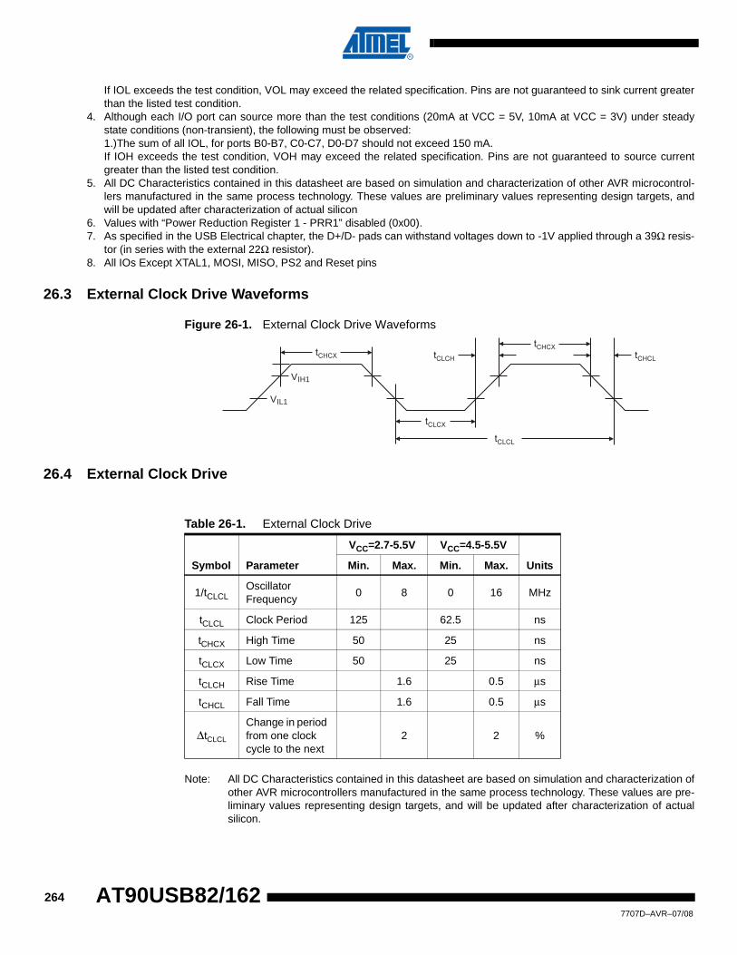
If IOL exceeds the test condition, VOL may exceed the related specification. Pins are not guaranteed to sink current greater than the listed test condition.
4. Although each I/O port can source more than the test conditions (20mA at VCC = 5V, 10mA at VCC = 3V) under steady state conditions (non-transient), the following must be observed: 1.)The sum of all IOL, for ports B0-B7, C0-C7, D0-D7 should not exceed 150 mA. If IOH exceeds the test condition, VOH may exceed the related specification. Pins are not guaranteed to source current greater than the listed test condition.
5. All DC Characteristics contained in this datasheet are based on simulation and characterization of other AVR microcontrol-lers manufactured in the same process technology. These values are preliminary values representing design targets, and will be updated after characterization of actual silicon
6. Values with “Power Reduction Register 1 - PRR1” disabled (0x00).7. As specified in the USB Electrical chapter, the D+/D- pads can withstand voltages down to -1V applied through a 39Ω resis-
tor (in series with the external 22Ω resistor).8. All IOs Except XTAL1, MOSI, MISO, PS2 and Reset pins
26.3 External Clock Drive Waveforms
Figure 26-1. External Clock Drive Waveforms
26.4 External Clock Drive
Note: All DC Characteristics contained in this datasheet are based on simulation and characterization of other AVR microcontrollers manufactured in the same process technology. These values are pre-liminary values representing design targets, and will be updated after characterization of actual silicon.
VIL1
VIH1
Table 26-1. External Clock Drive
Symbol Parameter
VCC=2.7-5.5V VCC=4.5-5.5V
UnitsMin. Max. Min. Max.
1/tCLCLOscillator Frequency
0 8 0 16 MHz
tCLCL Clock Period 125 62.5 ns
tCHCX High Time 50 25 ns
tCLCX Low Time 50 25 ns
tCLCH Rise Time 1.6 0.5 μs
tCHCL Fall Time 1.6 0.5 μs
ΔtCLCL
Change in period from one clock cycle to the next
2 2 %
2647707D–AVR–07/08
AT90USB82/162

AT90USB82/162
26.5 Maximum speed vs. VCC
Maximum frequency is depending on VCC. As shown in Figure 26-2, the Maximum Frequency vs. VCC curve is linear between 2.7V < VCC < 4.5V.
Figure 26-2. Maximum Frequency vs. VCC, AT90USB82/162
26.6 SPI Timing Characteristics
See Figure 26-3 and Figure 26-3 for details.
16 MHz
8 MHz
2.7V 4.5V 5.5V
Safe Operating Area
Table 26-2. SPI Timing Parameters
Description Mode Min Typ Max
1 SCK period Master See Table 16-4
ns
2 SCK high/low Master 50% duty cycle
3 Rise/Fall time Master TBD
4 Setup Master 10
5 Hold Master 10
6 Out to SCK Master 0.5 • tsck
7 SCK to out Master 10
8 SCK to out high Master 10
9 SS low to out Slave 15
10 SCK period Slave 4 • tck
11 SCK high/low(1) Slave 2 • tck
12 Rise/Fall time Slave TBD
13 Setup Slave 10
14 Hold Slave tck
15 SCK to out Slave 15
16 SCK to SS high Slave 20
17 SS high to tri-state Slave 10
18 SS low to SCK Slave 20
2657707D–AVR–07/08

Note: 1. In SPI Programming mode the minimum SCK high/low period is: - 2 tCLCL for fCK < 12 MHz - 3 tCLCL for fCK > 12 MHz
Figure 26-3. SPI Interface Timing Requirements (Master Mode)
Table 26-3. SPI Interface Timing Requirements (Slave Mode)
26.7 Hardware Boot EntranceTiming Characteristics
Figure 26-4. Hardware Boot Timing Requirements
MOSI(Data Output)
SCK(CPOL = 1)
MISO(Data Input)
SCK(CPOL = 0)
SS
MSB LSB
LSBMSB
...
...
6 1
2 2
34 5
87
MISO(Data Output)
SCK(CPOL = 1)
MOSI(Data Input)
SCK(CPOL = 0)
SS
MSB LSB
LSBMSB
...
...
10
11 11
1213 14
1715
9
X
16
RESET
ALE/HWB
tSHRH tHHRH
2667707D–AVR–07/08
AT90USB82/162

AT90USB82/162
Table 26-4. Hardware Boot Timings
Symbol Parameter Min Max
tSHRH HWB low Setup before Reset High 0
tHHRH HWB low Hold after Reset HighStartUpTime(SUT) +
Time Out
Delay(TOUT)
2677707D–AVR–07/08

27. AT90USB82/162 Typical Characteristics – Preliminary DataThe following charts show typical behavior. These figures are not tested during manufacturing. All current consumption measurements are performed with all I/O pins configured as inputs and with internal pull-ups enabled. A sine wave generator with rail-to-rail output is used as clock source.
All Active- and Idle current consumption measurements are done with all bits in the PRR regis-ters set and thus, the corresponding I/O modules are turned off. Also the Analog Comparator is disabled during these measurements.
The power consumption in Power-down mode is independent of clock selection.
The current consumption is a function of several factors such as: operating voltage, operating frequency, loading of I/O pins, switching rate of I/O pins, code executed and ambient tempera-ture. The dominating factors are operating voltage and frequency.
The current drawn from capacitive loaded pins may be estimated (for one pin) as CL*VCC*f where CL = load capacitance, VCC = operating voltage and f = average switching frequency of I/O pin.
The parts are characterized at frequencies higher than test limits. Parts are not guaranteed to function properly at frequencies higher than the ordering code indicates.
The difference between current consumption in Power-down mode with Watchdog Timer enabled and Power-down mode with Watchdog Timer disabled represents the differential cur-rent drawn by the Watchdog Timer.
2687707D–AVR–07/08
AT90USB82/162

AT90USB82/162
27.1 Input Voltage Levels
Figure 27-1. Input Low Voltage vs. Vcc, all I/Os excluding DP/DM and MOSI/MISO
Figure 27-2. Input High Voltage vs. Vcc, all I/Os excluding DP/DM and MOSI/MISO
0
0.5
1
1.5
2
2.5
2 2.5 3 3.5 4 4.5 5 5.5
VCC (V)
Thr
esho
ld (
V)
0
0.5
1
1.5
2
2.5
2.5 3 3.5 4 4.5 5 5.5
VCC (V)
Thr
esho
ld (
V)
2697707D–AVR–07/08

Figure 27-3. Input Low Voltage vs. Vcc for MOSI/MISO I/Os
Figure 27-4. Input High Voltage vs. Vcc, MOSI/MISO I/Os
0
0.5
1
1.5
2
2.5
2.5 3 3.5 4 4.5 5 5.5
VCC (V)
Thr
esho
ld (
V) 85°C
25°C
-40°C
0
0.5
1
1.5
2
2.5
2.5 3 3.5 4 4.5 5 5.5
VCC (V)
Thr
esho
ld (
V) 85
25
-40
0
0.5
1
1.5
2
2.5
2.5 3 3.5 4 4.5 5 5.5
VCC (V)
Thr
esho
ld (
V) 85°C
25°C
-40°C
2707707D–AVR–07/08
AT90USB82/162

AT90USB82/162
27.2 Output Voltage Levels
Figure 27-5. Output Low Voltage vs. Output Current, all I/Os excluding DP/DM, Vcc=3V
Figure 27-6. Output Low Voltage vs. Output Current, all I/Os excluding DP/DM, Vcc=5V
0
0.1
0.2
0.3
0.4
0.5
0.6
0.7
0.8
0.9
1
0 5 10 15 20 25
IOL (mA)
VO
L (V
)
85
25
-40
-0.1
0
0.1
0.2
0.3
0.4
0.5
0.6
0.7
0 5 10 15 20 25
IOL (mA)
VO
L (
V) 85
25
-40
2717707D–AVR–07/08

Figure 27-7. Output Low Voltage vs. Output Current, PS2 I/Os, Vcc=5V
-0.2
0
0.2
0.4
0.6
0.8
1
1.2
0 5 10 15 20 25
IOL (mA)
VO
L (
V) 85°C
25°C
-40°C
0
0.2
0.4
0.6
0.8
1
1.2
0 2 4 6 8 10 12 14 16 18 20
IOL (mA)
VO
L (
V) 85°C
25°C
-40°C
2727707D–AVR–07/08
AT90USB82/162

AT90USB82/162
Figure 27-8. Output High Voltage vs. Output Current, all I/Os excluding DP/DM, Vcc=3V
Figure 27-9. Output High Voltage vs. Output Current, all I/Os excluding DP/DM, Vcc=5V
0
0.5
1
1.5
2
2.5
3
3.5
0 5 10 15 20 25
IOH (mA)
VO
H (
V)
85
25
-40
4.2
4.3
4.4
4.5
4.6
4.7
4.8
4.9
5
0 5 10 15 20 25
IOH (mA)
VO
H (
V)
85
25
-40
2737707D–AVR–07/08

27.3 I/O Pull-up Current
Figure 27-10. Standard I/O Pull-Up Current vs. Pin Voltage, Vcc=5V
-20
0
20
40
60
80
100
120
140
0 1 2 3 4 5
VOP (V)
I OP (
uA) 85
25
-40
0
20
40
60
80
100
120
140
0 1 2 3 4 5
VOP (V)
I OP (
uA)
2747707D–AVR–07/08
AT90USB82/162

AT90USB82/162
27.4 Power-down Supply Current
Figure 27-11. Power-down Supply Current vs. Vcc, with BOD Disabled, WDT Disabled, Regula-tor Disabled
Figure 27-12. Power-down Supply Current vs. Vcc, with BOD Disabled, WDT Enabled, Regula-tor Disabled
0
2
4
6
8
10
12
14
16
18
20
2 2.5 3 3.5 4 4.5 5 5.5 6
VCC (V)
I CC (
uA)
85
25
0
5
10
15
20
25
30
35
40
45
50
2 2.5 3 3.5 4 4.5 5 5.5 6 6.5
VCC (V)
I CC (
uA) 85
25
2757707D–AVR–07/08

Figure 27-13. Power-down Supply Current vs. Vcc, with BOD Enabled, Watchdog Disabled
Figure 27-14. Power-down Supply Current vs. Vcc, with BOD Enabled, WDT Enabled, Regula-tor Disabled
0
10
20
30
40
50
60
70
3 3.5 4 4.5 5 5.5
VCC (V)
I CC (
uA) 85°C
25°C
0
10
20
30
40
50
60
70
3 3.5 4 4.5 5 5.5
VCC (V)
I CC (
uA
)
WATCHDOG TIMER ENABLED, BODEN
0
10
20
30
40
50
60
70
80
90
100
3 3.5 4 4.5 5 5.5 6
VCC (V)
I CC (
uA)
85
25
2767707D–AVR–07/08
AT90USB82/162

AT90USB82/162
Figure 27-15. Power-down Supply Current vs. Vcc, with BOD Enabled, Regulator Enabled
-5
5
15
25
35
45
55
65
75
2 2.5 3 3.5 4 4.5 5 5.5 6
VCC (V)
I CC (
uA
)
0
10
20
30
40
50
60
70
80
90
100
2 2.5 3 3.5 4 4.5 5 5.5 6
V (V)
I CC (
uA)
85
25
-40
2777707D–AVR–07/08

27.5 Idle Supply Current
Figure 27-16. Idle Supply Current vs. Frequency and Vcc, T=25°C, Regulator Disabled (below 4V)
0
1
2
3
4
5
6
0 2 4 6 8 10 12 14 16
Frequency (MHz)
I CC (
mA
)
5.5
5
4.5
4
3.3
2787707D–AVR–07/08
AT90USB82/162

AT90USB82/162
27.6 Active Supply Current
Figure 27-17. Active Supply Current vs Frequency and Vcc, T=25°C
27.7 Reset Supply Current
Figure 27-18. Reset Supply Current vs Frequency and Vcc
0
2
4
6
8
10
12
14
16
18
20
0 2 4 6 8 10 12 14 16
Frequency (MHz)
I CC (
mA
) 5.5
5
4.5
3.6
2.7
0
2
4
6
8
10
12
4 6 8 10 12 14 16
Frequency (MHz)
I CC (
mA
)
5.5
5
4.5
3.3
2.7
2797707D–AVR–07/08

Figure 27-19. Reset Pull-Up Current vs. Pin Voltage, Vcc=5V
27.8 Bandgap Voltage
Figure 27-20. Bandgap voltage vs. Vcc, vs. Temperature
0
20
40
60
80
100
120
0 1 2 3 4 5 6
VRESET (V)
I RE
SE
T (
uA) 85°C
-40°C
1.05
1.06
1.07
1.08
1.09
1.1
1.11
1.12
1.13
1.14
1.15
2 2.5 3 3.5 4 4.5 5 5.5
Vcc (V)
Ban
dgap
Vol
tage
(V
)
85
25
-40
2807707D–AVR–07/08
AT90USB82/162

AT90USB82/162
27.9 USB Regulator
Figure 27-21. USB Regulator Output Voltage vs. Input Voltage, No Load
Figure 27-22. USB Regulator Output Voltage vs. Input Voltage, Load=75 Ohms
Note: The 75 Ohms load is equivalent to the maximum average consumption of the USB peripheral in operation (full bus load)
2.7
2.8
2.9
3
3.1
3.2
3.3
3.4
3 3.5 4 4.5 5 5.5 6
Voltage (V)
Cur
rent
(V
) 85°C
-40°C
2.7
2.8
2.9
3
3.1
3.2
3.3
3.4
3 3.5 4 4.5 5 5.5 6
Voltage (V)
Out
put V
olag
e (V
)
85°C
-40°C
2
2.2
2.4
2.6
2.8
3
3.2
3.4
3 3.5 4 4.5 5 5.5 6
Voltage (V)
Cur
rent
(V
)
85
25
-40
2
2.2
2.4
2.6
2.8
3
3.2
3.4
3 3.5 4 4.5 5 5.5 6
Voltage (V)
Vol
tage
(V
)
85
25
-40
2817707D–AVR–07/08

27.10 Power-On Reset
Figure 27-23. Power-On Reset Level vs. Temperature
1
1.1
1.2
1.3
1.4
1.5
1.6
1.7
-50 -40 -30 -20 -10 0 10 20 30 40 50 60 70 80 90 100
Temperature
PO
R V
olta
ge (
V)
2827707D–AVR–07/08
AT90USB82/162

AT90USB82/162
27.11 BOD Levels
Figure 27-24. BOD Voltage (2.7V level) vs. Temperature
Figure 27-25. BOD Voltage (2.9V level) vs. Temperature
2.69
2.7
2.71
2.72
2.73
2.74
2.75
2.76
2.77
2.78
2.79
2.8
-50 -40 -30 -20 -10 0 10 20 30 40 50 60 70 80 90 100
Temperature (C)
Thr
esho
ld (
V)
Vcc Rise
Vcc Fall
2.88
2.9
2.92
2.94
2.96
2.98
3
-50 -40 -30 -20 -10 0 10 20 30 40 50 60 70 80 90 100
Temperature (C)
Thr
esho
ld (
V)
Vcc Rise
Vcc Fall
2837707D–AVR–07/08

Figure 27-26. BOD Voltage (3.0V level) vs. Temperature
Figure 27-27. BOD Voltage (3.5V level) vs. TemperatureBOD Voltage (3.0V level) vs. Temperature
2.98
3
3.02
3.04
3.06
3.08
3.1
3.12
-50 -40 -30 -20 -10 0 10 20 30 40 50 60 70 80 90 100
Temperature (C)
Thr
esho
ld (
V)
Vcc Rise
Vcc Fall
2.98
3
3.02
3.04
3.06
3.08
3.1
3.12
-50 -40 -30 -20 -10 0 10 20 30 40 50 60 70 80 90 100
Temperature (C)
Thr
esho
ld (
V)
Vcc Rise
Vcc Fall
2847707D–AVR–07/08
AT90USB82/162

AT90USB82/162
Figure 27-28. BOD Voltage (3.6V level) vs. Temperature
Figure 27-29. BOD Voltage (4.0V level) vs. Temperature
3.48
3.49
3.5
3.51
3.52
3.53
3.54
3.55
3.56
3.57
3.58
-50 -40 -30 -20 -10 0 10 20 30 40 50 60 70 80 90 100
Temperature (C)
Thr
esho
ld (
V)
Vcc Rise
Vcc Fall
3.58
3.59
3.6
3.61
3.62
3.63
3.64
3.65
3.66
3.67
3.68
3.69
-50 -40 -30 -20 -10 0 10 20 30 40 50 60 70 80 90 100
Temperature (C)
Thr
esho
ld (
V)
Vcc Rise
Vcc Fall
3.98
4
4.02
4.04
4.06
4.08
4.1
-50 -40 -30 -20 -10 0 10 20 30 40 50 60 70 80 90 100
Temperature (C)
Thr
esho
ld (
V)
Vcc Rise
Vcc Fall
2857707D–AVR–07/08

Figure 27-30. BOD Voltage (4.3V level) vs. Temperature
27.12 Watchdog Timer Frequency
Figure 27-31. WDT Oscillator Frequency vs. Vcc
3.48
3.49
3.5
3.51
3.52
3.53
3.54
3.55
3.56
3.57
3.58
-50 -40 -30 -20 -10 0 10 20 30 40 50 60 70 80 90 100
Temperature (C)
Thr
esho
ld (
V)
Vcc Rise
Vcc Fall
3.58
3.59
3.6
3.61
3.62
3.63
3.64
3.65
3.66
3.67
3.68
3.69
-50 -40 -30 -20 -10 0 10 20 30 40 50 60 70 80 90 100
Temperature (C)
Thr
esho
ld (
V)
Vcc Rise
Vcc Fall
3.98
4
4.02
4.04
4.06
4.08
4.1
-50 -40 -30 -20 -10 0 10 20 30 40 50 60 70 80 90 100
Temperature (C)
Thr
esho
ld (
V)
Vcc Rise
Vcc Fall
4.28
4.3
4.32
4.34
4.36
4.38
4.4
4.42
-50 -40 -30 -20 -10 0 10 20 30 40 50 60 70 80 90 100
Temperature (C)
Thr
esho
ld (
V)
Vcc Rise
Vcc Fall
114
116
118
120
122
124
126
128
2 2.5 3 3.5 4 4.5 5 5.5
VCC (V)
F RC (
kHz)
85
25
-40
2867707D–AVR–07/08
AT90USB82/162

AT90USB82/162
27.13 Internal RC Oscillator Frequency
Figure 27-32. RC Oscillator Frequency vs. OSCCAL, T=25°C
Figure 27-33. RC Oscillator Frequency vs. Vcc
0
5
10
15
20
-1 15 31 47 63 79 95 111 127 143 159 175 191 207 223 239 255
OSCCAL (X1)
F RC (
MH
z)
7.7
7.8
7.9
8
8.1
8.2
8.3
8.4
8.5
8.6
8.7
2 2.5 3 3.5 4 4.5 5 5.5
VCC (V)
F RC (
MH
z)
85°C
25°C
-40°C
2877707D–AVR–07/08

28. Register SummaryAddress Name Bit 7 Bit 6 Bit 5 Bit 4 Bit 3 Bit 2 Bit 1 Bit 0 Page
(0xFF) Reserved - - - - - - - -
(0xFE) Reserved - - - - - - - -
(0xFD) Reserved - - - - - - - -
(0xFC) Reserved - - - - - - - -
(0xFB) UPOE UPWE1 UPWE0 UPDRV1 UPDRV0 SCKI DATAI DPI DMI
(0xFA) PS2CON - - - - - - - PS2EN
(0xF9) Reserved - - - - - - - -
(0xF8) Reserved - - - - - - - -
(0xF7) Reserved - - - - - - - -
(0xF6) Reserved - - - - - - - -
(0xF5) Reserved - - - - - - - -
(0xF4) UEINT - - EPINT4:0
(0xF3) Reserved - - - - - - - -
(0xF2) UEBCLX BYCT7:0
(0xF1) UEDATX DAT7:0
(0xF0) UEIENX FLERRE NAKINE - NAKOUTE RXSTPE RXOUTE STALLEDE TXINE
(0xEF) UESTA1X - - - - - CTRLDIR CURRBK1:0
(0xEE) UESTA0X CFGOK OVERFI UNDERFI - DTSEQ1:0 NBUSYBK1:0
(0xED) UECFG1X - EPSIZE2:0 EPBK1:0 ALLOC -
(0xEC) UECFG0X EPTYPE1:0 - - - - - EPDIR
(0xEB) UECONX - - STALLRQ STALLRQC RSTDT - - EPEN
(0xEA) UERST - - - EPRST4:0
(0xE9) UENUM - - - - - EPNUM2:0
(0xE8) UEINTX FIFOCON NAKINI RWAL NAKOUTI RXSTPI RXOUTI STALLEDI TXINI
(0xE7) Reserved - - - - - - - -
(0xE6) UDMFN - - - FNCERR - - - -
(0xE5) UDFNUMH - - - - - FNUM10:8
(0xE4) UDFNUML FNUM7:0
(0xE3) UDADDR ADDEN UADD6:0
(0xE2) UDIEN - UPRSME EORSME WAKEUPE EORSTE SOFE - SUSPE
(0xE1) UDINT - UPRSMI EORSMI WAKEUPI EORSTI SOFI - SUSPI
(0xE0) UDCON - - - - - RSTCPU RMWKUP DETACH
(0xDF) Reserved - - - - - - - -
(0xDE) Reserved - - - - - - - -
(0xDD) Reserved - - - - - - - -
(0xDC) Reserved - - - - - - - -
(0xDB) Reserved - - - - - - - -
(0xDA) Reserved - - - - - - - -
(0xD9) Reserved - - - - - - - -
(0xD8) USBCON USBE - FRZCLK - - - - -
(0xD7) Reserved - - - - - - - -
(0xD6) Reserved - - - - - - - -
(0xD5) Reserved - - - - - - - -
(0xD4) Reserved - - - - - - - -
(0xD3) Reserved - - - - - - - -
(0xD2) CLKSTA - - - - - - RCON EXTON
(0xD1) CLKSEL1 RCCKSEL3 RCCKSEL2 RCCKSEL1 RCCKSEL0 EXCKSEL3 EXCKSEL2 EXCKSEL1 EXCKSEL0
(0xD0) CLKSEL0 RCSUT1 RCSUT0 EXSUT1 EXSUT0 RCE EXTE - CLKS
(0xCF) Reserved - - - - - - - -
(0xCE) UDR1 USART1 I/O Data Register
(0xCD) UBRR1H - - - - USART1 Baud Rate Register High Byte
(0xCC) UBRR1L USART1 Baud Rate Register Low Byte
(0xCB) UCSR1D - - - - - - CTSEN RTSEN
(0xCA) UCSR1C UMSEL11 UMSEL10 UPM11 UPM10 USBS1 UCSZ11 UCSZ10 UCPOL1
(0xC9) UCSR1B RXCIE1 TXCIE1 UDRIE1 RXEN1 TXEN1 UCSZ12 RXB81 TXB81
(0xC8) UCSR1A RXC1 TXC1 UDRE1 FE1 DOR1 PE1 U2X1 MPCM1
(0xC7) Reserved - - - - - - - -
(0xC6) Reserved - - - - - - - -
(0xC5) Reserved - - - - - - - -
(0xC4) Reserved - - - - - - - -
(0xC3) Reserved - - - - - - - -
(0xC2) Reserved - - - - - - - -
(0xC1) Reserved - - - - - - - -
(0xC0) Reserved - - - - - - - -
(0xBF) Reserved - - - - - - - -
2887707DS–AVR–07/08
AT90USB82/162

AT90USB82/162
(0xBE) Reserved - - - - - - - -
(0xBD) Reserved - - - - - - - -
(0xBC) Reserved - - - - - - - -
(0xBB) Reserved - - - - - - - -
(0xBA) Reserved - - - - - - - -
(0xB9) Reserved - - - - - - - -
(0xB8) Reserved - - - - - - - -
(0xB7) Reserved - - - - - - - -
(0xB6) Reserved - - - - - - - -
(0xB5) Reserved - - - - - - - -
(0xB4) Reserved - - - - - - - -
(0xB3) Reserved - - - - - - - -
(0xB2) Reserved - - - - - - - -
(0xB1) Reserved - - - - - - - -
(0xB0) Reserved - - - - - - - -
(0xAF) Reserved - - - - - - - -
(0xAE) Reserved - - - - - - - -
(0xAD) Reserved - - - - - - - -
(0xAC) Reserved - - - - - - - -
(0xAB) Reserved - - - - - - - -
(0xAA) Reserved - - - - - - - -
(0xA9) Reserved - - - - - - - -
(0xA8) Reserved - - - - - - - -
(0xA7) Reserved - - - - - - - -
(0xA6) Reserved - - - - - - - -
(0xA5) Reserved - - - - - - - -
(0xA4) Reserved - - - - - - - -
(0xA3) Reserved - - - - - - - -
(0xA2) Reserved - - - - - - - -
(0xA1) Reserved - - - - - - - -
(0xA0) Reserved - - - - - - - -
(0x9F) Reserved - - - - - - - -
(0x9E) Reserved - - - - - - - -
(0x9D) Reserved - - - - - - - -
(0x9C) Reserved - - - - - - - -
(0x9B) Reserved - - - - - - - -
(0x9A) Reserved - - - - - - - -
(0x99) Reserved - - - - - - - -
(0x98) Reserved - - - - - - - -
(0x97) Reserved - - - - - - - -
(0x96) Reserved - - - - - - - -
(0x95) Reserved - - - - - - - -
(0x94) Reserved - - - - - - - -
(0x93) Reserved - - - - - - - -
(0x92) Reserved - - - - - - - -
(0x91) Reserved - - - - - - - -
(0x90) Reserved - - - - - - - -
(0x8F) Reserved - - - - - - - -
(0x8E) Reserved - - - - - - - -
(0x8D) OCR1CH Timer/Counter1 - Output Compare Register C High Byte
(0x8C) OCR1CL Timer/Counter1 - Output Compare Register C Low Byte
(0x8B) OCR1BH Timer/Counter1 - Output Compare Register B High Byte
(0x8A) OCR1BL Timer/Counter1 - Output Compare Register B Low Byte
(0x89) OCR1AH Timer/Counter1 - Output Compare Register A High Byte
(0x88) OCR1AL Timer/Counter1 - Output Compare Register A Low Byte
(0x87) ICR1H Timer/Counter1 - Input Capture Register High Byte
(0x86) ICR1L Timer/Counter1 - Input Capture Register Low Byte
(0x85) TCNT1H Timer/Counter1 - Counter Register High Byte
(0x84) TCNT1L Timer/Counter1 - Counter Register Low Byte
(0x83) Reserved - - - - - - - -
(0x82) TCCR1C FOC1A FOC1B FOC1C - - - - -
(0x81) TCCR1B ICNC1 ICES1 - WGM13 WGM12 CS12 CS11 CS10
(0x80) TCCR1A COM1A1 COM1A0 COM1B1 COM1B0 COM1C1 COM1C0 WGM11 WGM10
(0x7F) Reserved - - - - - - - -
(0x7E) Reserved - - - - - - - -
(0x7D) Reserved - - - - - - - -
Address Name Bit 7 Bit 6 Bit 5 Bit 4 Bit 3 Bit 2 Bit 1 Bit 0 Page
2897707DS–AVR–07/08

(0x7C) Reserved - - - - - - - -
(0x7B) Reserved - - - - - - - -
(0x7A) Reserved - - - - - - - -
(0x79) Reserved - - - - - - - -
(0x78) Reserved - - - - - - - -
(0x77) Reserved - - - - - - - -
(0x76) Reserved - - - - - - - -
(0x75) Reserved - - - - - - - -
(0x74) Reserved - - - - - - - -
(0x73) Reserved - - - - - - - -
(0x72) Reserved - - - - - - - -
(0x71) Reserved - - - - - - - -
(0x70) Reserved - - - - - - - -
(0x6F) TIMSK1 - - ICIE1 - OCIE1C OCIE1B OCIE1A TOIE1
(0x6E) TIMSK0 - - - - - OCIE0B OCIE0A TOIE0
(0x6D) Reserved - - - - - - - -
(0x6C) PCMSK1 - - - PCINT12 PCINT11 PCINT10 PCINT9 PCINT8
(0x6B) PCMSK0 PCINT7 PCINT6 PCINT5 PCINT4 PCINT3 PCINT2 PCINT1 PCINT0
(0x6A) EICRB ISC71 ISC70 ISC61 ISC60 ISC51 ISC50 ISC41 ISC40
(0x69) EICRA ISC31 ISC30 ISC21 ISC20 ISC11 ISC10 ISC01 ISC00
(0x68) PCICR - - - - - - PCIE1 PCIE0
(0x67) Reserved - - - - - - - -
(0x66) OSCCAL Oscillator Calibration Register
(0x65) PRR1 PRUSB - - - - - - PRUSART1
(0x64) PRR0 - - PRTIM0 - PRTIM1 PRSPI - -
(0x63) REGCR - - - - - - - REGDIS
(0x62) WDTCKD - - - - WDEWIF WDEWIE WCLKD1 WCLKD0
(0x61) CLKPR CLKPCE - - - CLKPS3 CLKPS2 CLKPS1 CLKPS0
(0x60) WDTCSR WDIF WDIE WDP3 WDCE WDE WDP2 WDP1 WDP0
0x3F (0x5F) SREG I T H S V N Z C
0x3E (0x5E) SPH SP15 SP14 SP13 SP12 SP11 SP10 SP9 SP8
0x3D (0x5D) SPL SP7 SP6 SP5 SP4 SP3 SP2 SP1 SP0
0x3C (0x5C) Reserved - - - - - - - -
0x3B (0x5B) Reserved - - - - - - - -
0x3A (0x5A) Reserved - - - - - - - -
0x39 (0x59) Reserved - - - - - - - -
0x38 (0x58) Reserved - - - - - - - -
0x37 (0x57) SPMCSR SPMIE RWWSB SIGRD RWWSRE BLBSET PGWRT PGERS SPMEN
0x36 (0x56) Reserved - - - - - - - -
0x35 (0x55) MCUCR - - - - - - IVSEL IVCE
0x34 (0x54) MCUSR - - USBRF - WDRF BORF EXTRF PORF
0x33 (0x53) SMCR - - - - SM2 SM1 SM0 SE
0x32 (0x52) Reserved - - - - - - - -
0x31 (0x51) DWDR debugWIRE Data Register
0x30 (0x50) ACSR ACD ACBG ACO ACI ACIE ACIC ACIS1 ACIS0
0x2F (0x4F) Reserved - - - - - - - -
0x2E (0x4E) SPDR SPI Data Register
0x2D (0x4D) SPSR SPIF WCOL - - - - - SPI2X
0x2C (0x4C) SPCR SPIE SPE DORD MSTR CPOL CPHA SPR1 SPR0
0x2B (0x4B) GPIOR2 General Purpose I/O Register 2
0x2A (0x4A) GPIOR1 General Purpose I/O Register 1
0x29 (0x49) PLLCSR - - - PLLP2 PLLP1 PLLP0 PLLE PLOCK
0x28 (0x48) OCR0B Timer/Counter0 Output Compare Register B
0x27 (0x47) OCR0A Timer/Counter0 Output Compare Register A
0x26 (0x46) TCNT0 Timer/Counter0 (8 Bit)
0x25 (0x45) TCCR0B FOC0A FOC0B - - WGM02 CS02 CS01 CS00
0x24 (0x44) TCCR0A COM0A1 COM0A0 COM0B1 COM0B0 - - WGM01 WGM00
0x23 (0x43) GTCCR TSM - - - - - PSRASY PSRSYNC
0x22 (0x42) EEARH - - - - EEPROM Address Register High Byte
0x21 (0x41) EEARL EEPROM Address Register Low Byte
0x20 (0x40) EEDR EEPROM Data Register
0x1F (0x3F) EECR - - EEPM1 EEPM0 EERIE EEMPE EEPE EERE
0x1E (0x3E) GPIOR0 General Purpose I/O Register 0
0x1D (0x3D) EIMSK INT7 INT6 INT5 INT4 INT3 INT2 INT1 INT0
0x1C (0x3C) EIFR INTF7 INTF6 INTF5 INTF4 INTF3 INTF2 INTF1 INTF0
0x1B (0x3B) PCIFR - - - - - - PCIF1 PCIF0
Address Name Bit 7 Bit 6 Bit 5 Bit 4 Bit 3 Bit 2 Bit 1 Bit 0 Page
2907707DS–AVR–07/08
AT90USB82/162

AT90USB82/162
Note: 1. For compatibility with future devices, reserved bits should be written to zero if accessed. Moreover reserved bits are not guaranteed to be read as “0”. Reserved I/O memory addresses should never be written.
2. I/O registers within the address range $00 - $1F are directly bit-accessible using the SBI and CBI instructions. In these reg-isters, the value of single bits can be checked by using the SBIS and SBIC instructions.
3. Some of the status flags are cleared by writing a logical one to them. Note that the CBI and SBI instructions will operate on all bits in the I/O register, writing a one back into any flag read as set, thus clearing the flag. The CBI and SBI instructions work with registers 0x00 to 0x1F only.
4. When using the I/O specific commands IN and OUT, the I/O addresses $00 - $3F must be used. When addressing I/O reg-isters as data space using LD and ST instructions, $20 must be added to these addresses. The AT90USB82/162 is a complex microcontroller with more peripheral units than can be supported within the 64 location reserved in Opcode for the IN and OUT instructions. For the Extended I/O space from $60 - $1FF in SRAM, only the ST/STS/STD and LD/LDS/LDD instructions can be used.
0x1A (0x3A) Reserved - - - - - - - -
0x19 (0x39) Reserved - - - - - - - -
0x18 (0x38) Reserved - - - - - - - -
0x17 (0x37) Reserved - - - - - - - -
0x16 (0x36) TIFR1 - - ICF1 - OCF1C OCF1B OCF1A TOV1
0x15 (0x35) TIFR0 - - - - - OCF0B OCF0A TOV0
0x14 (0x34) Reserved - - - - - - - -
0x13 (0x33) Reserved - - - - - - - -
0x12 (0x32) Reserved - - - - - - - -
0x11 (0x31) Reserved - - - - - - - -
0x10 (0x30) Reserved - - - - - - - -
0x0F (0x2F) Reserved - - - - - - - -
0x0E (0x2E) Reserved - - - - - - - -
0x0D (0x2D) Reserved - - - - - - - -
0x0C (0x2C) Reserved - - - - - - - -
0x0B (0x2B) PORTD PORTD7 PORTD6 PORTD5 PORTD4 PORTD3 PORTD2 PORTD1 PORTD0
0x0A (0x2A) DDRD DDD7 DDD6 DDD5 DDD4 DDD3 DDD2 DDD1 DDD0
0x09 (0x29) PIND PIND7 PIND6 PIND5 PIND4 PIND3 PIND2 PIND1 PIND0
0x08 (0x28) PORTC PORTC7 PORTC6 PORTC5 PORTC4 - PORTC2 PORTC1 PORTC0
0x07 (0x27) DDRC DDC7 DDC6 DDC5 DDC4 - DDC2 DDC1 DDC0
0x06 (0x26) PINC PINC7 PINC6 PINC5 PINC4 - PINC2 PINC1 PINC0
0x05 (0x25) PORTB PORTB7 PORTB6 PORTB5 PORTB4 PORTB3 PORTB2 PORTB1 PORTB0
0x04 (0x24) DDRB DDB7 DDB6 DDB5 DDB4 DDB3 DDB2 DDB1 DDB0
0x03 (0x23) PINB PINB7 PINB6 PINB5 PINB4 PINB3 PINB2 PINB1 PINB0
0x02 (0x22) Reserved - - - - - - - -
0x01 (0x21) Reserved - - - - - - - -
0x00 (0x20) Reserved - - - - - - - -
Address Name Bit 7 Bit 6 Bit 5 Bit 4 Bit 3 Bit 2 Bit 1 Bit 0 Page
2917707DS–AVR–07/08

29. Instruction Set SummaryMnemonics Operands Description Operation Flags #Clocks
ARITHMETIC AND LOGIC INSTRUCTIONS
ADD Rd, Rr Add two Registers Rd ← Rd + Rr Z,C,N,V,H 1
ADC Rd, Rr Add with Carry two Registers Rd ← Rd + Rr + C Z,C,N,V,H 1
ADIW Rdl,K Add Immediate to Word Rdh:Rdl ← Rdh:Rdl + K Z,C,N,V,S 2
SUB Rd, Rr Subtract two Registers Rd ← Rd - Rr Z,C,N,V,H 1
SUBI Rd, K Subtract Constant from Register Rd ← Rd - K Z,C,N,V,H 1
SBC Rd, Rr Subtract with Carry two Registers Rd ← Rd - Rr - C Z,C,N,V,H 1
SBCI Rd, K Subtract with Carry Constant from Reg. Rd ← Rd - K - C Z,C,N,V,H 1
SBIW Rdl,K Subtract Immediate from Word Rdh:Rdl ← Rdh:Rdl - K Z,C,N,V,S 2
AND Rd, Rr Logical AND Registers Rd ← Rd • Rr Z,N,V 1
ANDI Rd, K Logical AND Register and Constant Rd ← Rd • K Z,N,V 1
OR Rd, Rr Logical OR Registers Rd ← Rd v Rr Z,N,V 1
ORI Rd, K Logical OR Register and Constant Rd ← Rd v K Z,N,V 1
EOR Rd, Rr Exclusive OR Registers Rd ← Rd ⊕ Rr Z,N,V 1
COM Rd One’s Complement Rd ← 0xFF − Rd Z,C,N,V 1
NEG Rd Two’s Complement Rd ← 0x00 − Rd Z,C,N,V,H 1
SBR Rd,K Set Bit(s) in Register Rd ← Rd v K Z,N,V 1
CBR Rd,K Clear Bit(s) in Register Rd ← Rd • (0xFF - K) Z,N,V 1
INC Rd Increment Rd ← Rd + 1 Z,N,V 1
DEC Rd Decrement Rd ← Rd − 1 Z,N,V 1
TST Rd Test for Zero or Minus Rd ← Rd • Rd Z,N,V 1
CLR Rd Clear Register Rd ← Rd ⊕ Rd Z,N,V 1
SER Rd Set Register Rd ← 0xFF None 1
BRANCH INSTRUCTIONS
RJMP k Relative Jump PC ← PC + k + 1 None 2
IJMP Indirect Jump to (Z) PC ← Z None 2
JMP k Direct Jump PC ← k None 3
RCALL k Relative Subroutine Call PC ← PC + k + 1 None 4
ICALL Indirect Call to (Z) PC ← Z None 4
CALL k Direct Subroutine Call PC ← k None 5
RET Subroutine Return PC ← STACK None 5
RETI Interrupt Return PC ← STACK I 5
CPSE Rd,Rr Compare, Skip if Equal if (Rd = Rr) PC ← PC + 2 or 3 None 1/2/3
CP Rd,Rr Compare Rd − Rr Z, N,V,C,H 1
CPC Rd,Rr Compare with Carry Rd − Rr − C Z, N,V,C,H 1
CPI Rd,K Compare Register with Immediate Rd − K Z, N,V,C,H 1
SBRC Rr, b Skip if Bit in Register Cleared if (Rr(b)=0) PC ← PC + 2 or 3 None 1/2/3
SBRS Rr, b Skip if Bit in Register is Set if (Rr(b)=1) PC ← PC + 2 or 3 None 1/2/3
SBIC P, b Skip if Bit in I/O Register Cleared if (P(b)=0) PC ← PC + 2 or 3 None 1/2/3
SBIS P, b Skip if Bit in I/O Register is Set if (P(b)=1) PC ← PC + 2 or 3 None 1/2/3
BRBS s, k Branch if Status Flag Set if (SREG(s) = 1) then PC←PC+k + 1 None 1/2
BRBC s, k Branch if Status Flag Cleared if (SREG(s) = 0) then PC←PC+k + 1 None 1/2
BREQ k Branch if Equal if (Z = 1) then PC ← PC + k + 1 None 1/2
BRNE k Branch if Not Equal if (Z = 0) then PC ← PC + k + 1 None 1/2
BRCS k Branch if Carry Set if (C = 1) then PC ← PC + k + 1 None 1/2
BRCC k Branch if Carry Cleared if (C = 0) then PC ← PC + k + 1 None 1/2
BRSH k Branch if Same or Higher if (C = 0) then PC ← PC + k + 1 None 1/2
BRLO k Branch if Lower if (C = 1) then PC ← PC + k + 1 None 1/2
BRMI k Branch if Minus if (N = 1) then PC ← PC + k + 1 None 1/2
BRPL k Branch if Plus if (N = 0) then PC ← PC + k + 1 None 1/2
BRGE k Branch if Greater or Equal, Signed if (N ⊕ V= 0) then PC ← PC + k + 1 None 1/2
BRLT k Branch if Less Than Zero, Signed if (N ⊕ V= 1) then PC ← PC + k + 1 None 1/2
BRHS k Branch if Half Carry Flag Set if (H = 1) then PC ← PC + k + 1 None 1/2
BRHC k Branch if Half Carry Flag Cleared if (H = 0) then PC ← PC + k + 1 None 1/2
BRTS k Branch if T Flag Set if (T = 1) then PC ← PC + k + 1 None 1/2
BRTC k Branch if T Flag Cleared if (T = 0) then PC ← PC + k + 1 None 1/2
BRVS k Branch if Overflow Flag is Set if (V = 1) then PC ← PC + k + 1 None 1/2
BRVC k Branch if Overflow Flag is Cleared if (V = 0) then PC ← PC + k + 1 None 1/2
BRIE k Branch if Interrupt Enabled if ( I = 1) then PC ← PC + k + 1 None 1/2
BRID k Branch if Interrupt Disabled if ( I = 0) then PC ← PC + k + 1 None 1/2
BIT AND BIT-TEST INSTRUCTIONS
SBI P,b Set Bit in I/O Register I/O(P,b) ← 1 None 2
CBI P,b Clear Bit in I/O Register I/O(P,b) ← 0 None 2
LSL Rd Logical Shift Left Rd(n+1) ← Rd(n), Rd(0) ← 0 Z,C,N,V 1
LSR Rd Logical Shift Right Rd(n) ← Rd(n+1), Rd(7) ← 0 Z,C,N,V 1
2927707DS–AVR–07/08
AT90USB82/162
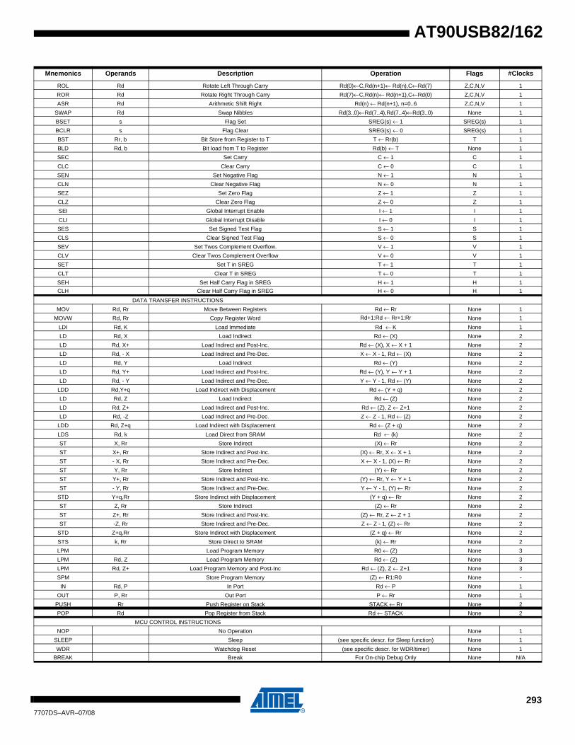
AT90USB82/162
ROL Rd Rotate Left Through Carry Rd(0)←C,Rd(n+1)← Rd(n),C←Rd(7) Z,C,N,V 1
ROR Rd Rotate Right Through Carry Rd(7)←C,Rd(n)← Rd(n+1),C←Rd(0) Z,C,N,V 1
ASR Rd Arithmetic Shift Right Rd(n) ← Rd(n+1), n=0..6 Z,C,N,V 1
SWAP Rd Swap Nibbles Rd(3..0)←Rd(7..4),Rd(7..4)←Rd(3..0) None 1
BSET s Flag Set SREG(s) ← 1 SREG(s) 1
BCLR s Flag Clear SREG(s) ← 0 SREG(s) 1
BST Rr, b Bit Store from Register to T T ← Rr(b) T 1
BLD Rd, b Bit load from T to Register Rd(b) ← T None 1
SEC Set Carry C ← 1 C 1
CLC Clear Carry C ← 0 C 1
SEN Set Negative Flag N ← 1 N 1
CLN Clear Negative Flag N ← 0 N 1
SEZ Set Zero Flag Z ← 1 Z 1
CLZ Clear Zero Flag Z ← 0 Z 1
SEI Global Interrupt Enable I ← 1 I 1
CLI Global Interrupt Disable I ← 0 I 1
SES Set Signed Test Flag S ← 1 S 1
CLS Clear Signed Test Flag S ← 0 S 1
SEV Set Twos Complement Overflow. V ← 1 V 1
CLV Clear Twos Complement Overflow V ← 0 V 1
SET Set T in SREG T ← 1 T 1
CLT Clear T in SREG T ← 0 T 1
SEH Set Half Carry Flag in SREG H ← 1 H 1
CLH Clear Half Carry Flag in SREG H ← 0 H 1
DATA TRANSFER INSTRUCTIONS
MOV Rd, Rr Move Between Registers Rd ← Rr None 1
MOVW Rd, Rr Copy Register Word Rd+1:Rd ← Rr+1:Rr None 1
LDI Rd, K Load Immediate Rd ← K None 1
LD Rd, X Load Indirect Rd ← (X) None 2
LD Rd, X+ Load Indirect and Post-Inc. Rd ← (X), X ← X + 1 None 2
LD Rd, - X Load Indirect and Pre-Dec. X ← X - 1, Rd ← (X) None 2
LD Rd, Y Load Indirect Rd ← (Y) None 2
LD Rd, Y+ Load Indirect and Post-Inc. Rd ← (Y), Y ← Y + 1 None 2
LD Rd, - Y Load Indirect and Pre-Dec. Y ← Y - 1, Rd ← (Y) None 2
LDD Rd,Y+q Load Indirect with Displacement Rd ← (Y + q) None 2
LD Rd, Z Load Indirect Rd ← (Z) None 2
LD Rd, Z+ Load Indirect and Post-Inc. Rd ← (Z), Z ← Z+1 None 2
LD Rd, -Z Load Indirect and Pre-Dec. Z ← Z - 1, Rd ← (Z) None 2
LDD Rd, Z+q Load Indirect with Displacement Rd ← (Z + q) None 2
LDS Rd, k Load Direct from SRAM Rd ← (k) None 2
ST X, Rr Store Indirect (X) ← Rr None 2
ST X+, Rr Store Indirect and Post-Inc. (X) ← Rr, X ← X + 1 None 2
ST - X, Rr Store Indirect and Pre-Dec. X ← X - 1, (X) ← Rr None 2
ST Y, Rr Store Indirect (Y) ← Rr None 2
ST Y+, Rr Store Indirect and Post-Inc. (Y) ← Rr, Y ← Y + 1 None 2
ST - Y, Rr Store Indirect and Pre-Dec. Y ← Y - 1, (Y) ← Rr None 2
STD Y+q,Rr Store Indirect with Displacement (Y + q) ← Rr None 2
ST Z, Rr Store Indirect (Z) ← Rr None 2
ST Z+, Rr Store Indirect and Post-Inc. (Z) ← Rr, Z ← Z + 1 None 2
ST -Z, Rr Store Indirect and Pre-Dec. Z ← Z - 1, (Z) ← Rr None 2
STD Z+q,Rr Store Indirect with Displacement (Z + q) ← Rr None 2
STS k, Rr Store Direct to SRAM (k) ← Rr None 2
LPM Load Program Memory R0 ← (Z) None 3
LPM Rd, Z Load Program Memory Rd ← (Z) None 3
LPM Rd, Z+ Load Program Memory and Post-Inc Rd ← (Z), Z ← Z+1 None 3
SPM Store Program Memory (Z) ← R1:R0 None -
IN Rd, P In Port Rd ← P None 1
OUT P, Rr Out Port P ← Rr None 1
PUSH Rr Push Register on Stack STACK ← Rr None 2
POP Rd Pop Register from Stack Rd ← STACK None 2
MCU CONTROL INSTRUCTIONS
NOP No Operation None 1
SLEEP Sleep (see specific descr. for Sleep function) None 1
WDR Watchdog Reset (see specific descr. for WDR/timer) None 1
BREAK Break For On-chip Debug Only None N/A
Mnemonics Operands Description Operation Flags #Clocks
2937707DS–AVR–07/08
30. Ordering Information
31. Packaging Information
Part Number Temp. Range Flash Memory Size Package Product Marking
90USB82-16MU Industrial Green 8K QFN32 90USB82-16MU
90USB162-16MU Industrial Green 16K QFN32 90USB162-16MU
90USB162-16AU Industrial Green 16K TQFP32 90USB162-16AU
Package Type
QFN32PN, 32-Lead 5.0 x 5.0 mm Body, 0.50 mm PitchQuad Flat No Lead Package (QFN)
TQFP32MA, 32-Lead 7 x 7 mm Body size, 1.00 mm Bodu Thickness0.5 mm Lead Pitch, Thin Profile Plastic Quad Flat Package (TQFP)
2947707DS–AVR–07/08
AT90USB82/162

AT90USB82/162
31.1 QFN32
*
2957707DS–AVR–07/08

31.2 TQFP32
2967707DS–AVR–07/08
AT90USB82/162

AT90USB82/162
32. Errata
32.1 AT90USB162 Errata History
32.1.1 AT90USB162 First Release
1. High current consumption in sleep modeIf a pending interrupt cannot wake the part up from the selected mode, the current consump-tion will increase during sleep when executing the SLEEP instruction directly after a SEI instruction.
Problem Fix/workaroundBefore entering sleep, interrupts not used to wake up the part from the sleep mode should be disabled.
2. PS2 high level clamped to UCAPWhen configured in PS2 mode, the output high level is clamped to the UCAP voltage level.
Problem Fix/workaroundNone.
3. Transient perturbation in USB suspend mode generates overconsumptionIn device mode and when the USB is suspended, transient perturbation received on the USB lines generates a wake up state. However the idle state following the perturbation does not set the SUSPI bit anymore. The internal USB engine remains in suspend mode but the USB differential receiver is still enabled and generates a typical 300µA extra-power con-sumption. Detection of the suspend state after the transient perturbation should be performed by software (instead of reading the SUSPI bit).
Problem fix/workaroundUSB waiver allows bus powered devices to consume up to 2.5mA in suspend state.
32.1.2 AT90USB162 Second Release
1. High current consumption in sleep modeIf a pending interrupt cannot wake the part up from the selected mode, the current consump-tion will increase during sleep when executing the SLEEP instruction directly after a SEI instruction.
Problem Fix/workaround
Silicon
Release
QFP32
‘DateCode LotNumber’ marking
QFN32
‘DateCode LotNumber’ marking
First Release
‘0705 6J4972’
‘0709 J4973-2’
‘0709 J5597-1’
all lots marked
90USB162–16MES
Second Release ‘0709 F3150-1’
‘0714 50-2’
‘0722 50-3’
‘0735 3151’
Third Release All date codes after 0709 All other lots
2977707DS–AVR–07/08

Before entering sleep, interrupts not used to wake up the part from the sleep mode should be disabled.
2. Extra power consumptionThe typical power comsumption is increased by 90µA at 5V and by 160µA in worst case conditions.
Problem Fix/workaroundNone.
3. Transient perturbation in USB suspend mode generates overconsumptionIn device mode and when the USB is suspended, transient perturbation received on the USB lines generates a wake up state. However the idle state following the perturbation does not set the SUSPI bit anymore. The internal USB engine remains in suspend mode but the USB differential receiver is still enabled and generates a typical 300µA extra-power con-sumption. Detection of the suspend state after the transient perturbation should be performed by software (instead of reading the SUSPI bit).
Problem fix/workaroundUSB waiver allows bus powered devices to consume up to 2.5mA in suspend state.
32.1.3 AT90USB162 Third Release
1. High current consumption in sleep modeIf a pending interrupt cannot wake the part up from the selected mode, the current consump-tion will increase during sleep when executing the SLEEP instruction directly after a SEI instruction.
Problem Fix/workaroundBefore entering sleep, interrupts not used to wake up the part from the sleep mode should be disabled.
2. Transient perturbation in USB suspend mode generates overconsumptionIn device mode and when the USB is suspended, transient perturbation received on the USB lines generates a wake up state. However the idle state following the perturbation does not set the SUSPI bit anymore. The internal USB engine remains in suspend mode but the USB differential receiver is still enabled and generates a typical 300µA extra-power con-sumption. Detection of the suspend state after the transient perturbation should be performed by software (instead of reading the SUSPI bit).
Problem fix/workaroundUSB waiver allows bus powered devices to consume up to 2.5mA in suspend state.
32.2 AT90USB82 Errata History
32.2.1 AT90USB82 Initial Release (all lots)
1. High current consumption in sleep modeIf a pending interrupt cannot wake the part up from the selected mode, the current consump-tion will increase during sleep when executing the SLEEP instruction directly after a SEI instruction.
2987707DS–AVR–07/08
AT90USB82/162

AT90USB82/162
Problem Fix/workaroundBefore entering sleep, interrupts not used to wake up the part from the sleep mode should be disabled.
2. Transient perturbation in USB suspend mode generates overconsumptionIn device mode and when the USB is suspended, transient perturbation received on the USB lines generates a wake up state. However the idle state following the perturbation does not set the SUSPI bit anymore. The internal USB engine remains in suspend mode but the USB differential receiver is still enabled and generates a typical 300µA extra-power con-sumption. Detection of the suspend state after the transient perturbation should be performed by software (instead of reading the SUSPI bit).
Problem fix/workaroundUSB waiver allows bus powered devices to consume up to 2.5mA in suspend state.
33. Datasheet Revision History for AT90USB82/162Please note that the referring page numbers in this section are referred to this document. The referring revision in this section are referring to the document revision.
33.1 Changes from 7707A to 7707B1. Removed all references to Timer/Counter 2, A/D Converter.
2. Clarified information in Power Reduction Mode and Timer/Counter 1 sections.
3. Added USB design guidelines and schematics.
4. Updated default fuse configuration & EEPROM page size.
5. Updated AC/DC parameters.
6. Updated Errata section.
33.2 Changes from 7707B to 7707C1. Updated Errata section.
33.3 Changes from 7707C to 7707D1. Correction to Oscillator description, page 245.
2997707DS–AVR–07/08

Features ..................................................................................................... 1
1 Pin Configurations ................................................................................... 3
1.1 Disclaimer ................................................................................................................3
2 Overview ................................................................................................... 4
2.1 Block Diagram .........................................................................................................4
2.2 Pin Descriptions .......................................................................................................5
3 About Code Examples ............................................................................. 7
4 AVR CPU Core .......................................................................................... 8
4.1 Introduction ..............................................................................................................8
4.2 Architectural Overview .............................................................................................8
4.3 ALU – Arithmetic Logic Unit .....................................................................................9
4.4 Status Register ........................................................................................................9
4.5 General Purpose Register File ..............................................................................11
4.6 Stack Pointer .........................................................................................................12
4.7 Instruction Execution Timing .................................................................................12
4.8 Reset and Interrupt Handling .................................................................................13
5 AVR AT90USB82/162 Memories ........................................................... 16
5.1 In-System Reprogrammable Flash Program Memory ...........................................16
5.2 SRAM Data Memory ..............................................................................................17
5.3 EEPROM Data Memory ........................................................................................18
5.4 I/O Memory ............................................................................................................24
6 System Clock and Clock Options ......................................................... 25
6.1 Clock Systems and their Distribution .....................................................................25
6.2 Clock Switch ..........................................................................................................26
6.3 Clock Sources .......................................................................................................29
6.4 Low Power Crystal Oscillator .................................................................................30
6.5 Calibrated Internal RC Oscillator ...........................................................................32
6.6 External Clock .......................................................................................................34
6.7 Clock Output Buffer ...............................................................................................34
6.8 System Clock Prescaler ........................................................................................34
6.9 PLL ........................................................................................................................36
7 Power Distribution ................................................................................. 39
8 Power Management and Sleep Modes ................................................. 41
17707D–AVR–07/08
AT90USB82/162
AT90USB82/162
8.1 Idle Mode ...............................................................................................................42
8.2 Power-down Mode .................................................................................................42
8.3 Power-save Mode ..................................................................................................42
8.4 Standby Mode .......................................................................................................42
8.5 Extended Standby Mode .......................................................................................42
8.6 Power Reduction Register .....................................................................................43
8.7 Minimizing Power Consumption ............................................................................44
9 System Control and Reset .................................................................... 46
9.1 Resetting the AVR .................................................................................................46
9.2 Reset Sources .......................................................................................................46
9.3 Power-on Reset .....................................................................................................47
9.4 External Reset .......................................................................................................48
9.5 Brown-out Detection ..............................................................................................49
9.6 Watchdog Reset ....................................................................................................50
9.7 USB Reset .............................................................................................................50
9.8 Internal Voltage Reference ....................................................................................52
9.9 Watchdog Timer ....................................................................................................52
10 Interrupts ................................................................................................ 63
10.1 Interrupt Vectors in AT90USB82/162 ..................................................................63
11 I/O-Ports .................................................................................................. 67
11.1 Introduction ..........................................................................................................67
11.2 Ports as General Digital I/O .................................................................................68
11.3 Alternate Port Functions ......................................................................................72
11.4 Register Description for I/O-Ports ........................................................................82
12 External Interrupts ................................................................................. 84
13 Timer/Counter0 and Timer/Counter1 Prescalers ................................ 88
14 8-bit Timer/Counter0 with PWM ............................................................ 90
14.1 Overview ..............................................................................................................90
14.2 Timer/Counter Clock Sources .............................................................................91
14.3 Counter Unit ........................................................................................................91
14.4 Output Compare Unit ...........................................................................................92
14.5 Compare Match Output Unit ................................................................................94
14.6 Modes of Operation .............................................................................................95
14.7 Timer/Counter Timing Diagrams .........................................................................99
27707D–AVR–07/08

14.8 8-bit Timer/Counter Register Description ..........................................................100
15 16-bit Timer/Counter 1 with PWM ....................................................... 107
15.1 Overview ............................................................................................................107
15.2 Accessing 16-bit Registers ................................................................................109
15.3 Timer/Counter Clock Sources ...........................................................................112
15.4 Counter Unit ......................................................................................................113
15.5 Input Capture Unit .............................................................................................114
15.6 Output Compare Units .......................................................................................116
15.7 Compare Match Output Unit ..............................................................................118
15.8 Modes of Operation ...........................................................................................119
15.9 Timer/Counter Timing Diagrams .......................................................................126
15.10 16-bit Timer/Counter Register Description ......................................................128
16 Serial Peripheral Interface – SPI ......................................................... 137
16.1 SS Pin Functionality ..........................................................................................141
16.2 Data Modes .......................................................................................................144
17 USART ................................................................................................... 146
17.1 Overview ............................................................................................................146
17.2 Clock Generation ...............................................................................................147
17.3 Frame Formats ..................................................................................................150
17.4 USART Initialization ...........................................................................................152
17.5 Data Transmission – The USART Transmitter ..................................................153
17.6 Data Reception – The USART Receiver ...........................................................155
17.7 Asynchronous Data Reception ..........................................................................159
17.8 Multi-processor Communication Mode ..............................................................162
17.9 Hardware Flow Control ......................................................................................163
17.10 USART Register Description ...........................................................................165
17.11 Examples of Baud Rate Setting .......................................................................169
18 USART in SPI Mode ............................................................................. 173
18.1 Overview ............................................................................................................173
18.2 Clock Generation ...............................................................................................174
18.3 SPI Data Modes and Timing ..............................................................................175
18.4 Frame Formats ..................................................................................................175
18.5 Data Transfer .....................................................................................................177
18.6 USART MSPIM Register Description ................................................................179
18.7 AVR USART MSPIM vs.
37707D–AVR–07/08
AT90USB82/162

AT90USB82/162
AVR SPI 181
19 USB controller ...................................................................................... 183
19.1 Features ............................................................................................................183
19.2 Block Diagram ...................................................................................................183
19.3 Typical Application Implementation ...................................................................184
19.4 General Operating Modes .................................................................................187
19.5 Power modes .....................................................................................................190
19.6 Memory management ........................................................................................190
19.7 PAD suspend .....................................................................................................191
19.8 D+/D- Read/write ...............................................................................................192
19.9 Registers description .........................................................................................193
19.10 USB Software Operating modes .....................................................................194
20 USB Device Operating modes ............................................................ 196
20.1 Introduction ........................................................................................................196
20.2 Power-on and reset ...........................................................................................196
20.3 Endpoint reset ...................................................................................................196
20.4 USB reset ..........................................................................................................197
20.5 Endpoint selection .............................................................................................197
20.6 Endpoint activation ............................................................................................197
20.7 Address Setup ...................................................................................................198
20.8 Suspend, Wake-up and Resume .......................................................................199
20.9 Detach ...............................................................................................................199
20.10 Remote Wake-up .............................................................................................200
20.11 STALL request .................................................................................................200
20.12 CONTROL endpoint management ..................................................................201
20.13 OUT endpoint management ............................................................................202
20.14 IN endpoint management ................................................................................204
20.15 Isochronous mode ...........................................................................................206
20.16 Overflow ..........................................................................................................206
20.17 Interrupts .........................................................................................................207
20.18 Registers .........................................................................................................208
21 PS/2 ....................................................................................................... 220
21.1 Characteristics ...................................................................................................220
22 Analog Comparator .............................................................................. 223
47707D–AVR–07/08

23 Boot Loader Support – Read-While-Write Self-Programming ......... 225
23.1 Boot Loader Features ........................................................................................225
23.2 Application and Boot Loader Flash Sections .....................................................225
23.3 Read-While-Write and No Read-While-Write Flash Sections ............................225
23.4 Boot Loader Lock Bits .......................................................................................228
23.5 Entering the Boot Loader Program ....................................................................229
23.6 Addressing the Flash During Self-Programming ...............................................233
23.7 Self-Programming the Flash ..............................................................................233
24 debugWIRE On-chip Debug System .................................................. 241
24.1 Features ............................................................................................................241
24.2 Overview ............................................................................................................241
24.3 Physical Interface ..............................................................................................241
24.4 Software Break Points .......................................................................................242
24.5 Limitations of debugWIRE .................................................................................242
24.6 debugWIRE Related Register in I/O Memory ....................................................242
25 Memory Programming ......................................................................... 243
25.1 Program And Data Memory Lock Bits ...............................................................243
25.2 Fuse Bits ............................................................................................................244
25.3 Signature Bytes .................................................................................................246
25.4 Calibration Byte .................................................................................................246
25.5 Parallel Programming Parameters, Pin Mapping, and Commands ...................246
25.6 Parallel Programming ........................................................................................249
25.7 Serial Downloading ............................................................................................257
25.8 Serial Programming Pin Mapping ......................................................................257
26 Electrical Characteristics .................................................................... 262
26.1 Absolute Maximum Ratings* .............................................................................262
26.2 DC Characteristics .............................................................................................262
26.3 External Clock Drive Waveforms .......................................................................264
26.4 External Clock Drive ..........................................................................................264
26.5 Maximum speed vs. VCC ...........................................................................................................................265
26.6 SPI Timing Characteristics ................................................................................265
26.7 Hardware Boot EntranceTiming Characteristics ................................................266
27 AT90USB82/162 Typical Characteristics – Preliminary Data ........... 268
27.1 Input Voltage Levels ..........................................................................................269
27.2 Output Voltage Levels .......................................................................................271
57707D–AVR–07/08
AT90USB82/162

AT90USB82/162
27.3 I/O Pull-up Current .............................................................................................274
27.4 Power-down Supply Current ..............................................................................275
27.5 Idle Supply Current ............................................................................................278
27.6 Active Supply Current ........................................................................................279
27.7 Reset Supply Current ........................................................................................279
27.8 Bandgap Voltage ...............................................................................................280
27.9 USB Regulator ...................................................................................................281
27.10 Power-On Reset ..............................................................................................282
27.11 BOD Levels .....................................................................................................283
27.12 Watchdog Timer Frequency ............................................................................286
27.13 Internal RC Oscillator Frequency ....................................................................287
28 Register Summary ............................................................................... 288
29 Instruction Set Summary ..................................................................... 292
30 Ordering Information ........................................................................... 294
31 Packaging Information ........................................................................ 294
31.1 QFN32 ...............................................................................................................295
31.2 TQFP32 .............................................................................................................296
32 Errata ..................................................................................................... 297
32.1 AT90USB162 Errata History ..............................................................................297
32.2 AT90USB82 Errata History ................................................................................298
33 Datasheet Revision History for AT90USB82/162 .............................. 299
33.1 Changes from 7707A to 7707B .........................................................................299
33.2 Changes from 7707B to 7707C .........................................................................299
33.3 Changes from 7707C to 7707D .........................................................................299
67707D–AVR–07/08
Headquarters International
Atmel Corporation2325 Orchard ParkwaySan Jose, CA 95131USATel: 1(408) 441-0311Fax: 1(408) 487-2600
Atmel AsiaRoom 1219Chinachem Golden Plaza77 Mody Road TsimshatsuiEast KowloonHong KongTel: (852) 2721-9778Fax: (852) 2722-1369
Atmel EuropeLe Krebs8, Rue Jean-Pierre TimbaudBP 30978054 Saint-Quentin-en-Yvelines CedexFranceTel: (33) 1-30-60-70-00 Fax: (33) 1-30-60-71-11
Atmel Japan9F, Tonetsu Shinkawa Bldg.1-24-8 ShinkawaChuo-ku, Tokyo 104-0033JapanTel: (81) 3-3523-3551Fax: (81) 3-3523-7581
Product Contact
Web Sitewww.atmel.com
Technical SupportEnter Product Line E-mail
Sales Contactwww.atmel.com/contacts
Literature Requestswww.atmel.com/literature
Disclaimer: The information in this document is provided in connection with Atmel products. No license, express or implied, by estoppel or otherwise, to any intellectual property right is granted by this document or in connection with the sale of Atmel products. EXCEPT AS SET FORTH IN ATMEL’S TERMS AND CONDI-TIONS OF SALE LOCATED ON ATMEL’S WEB SITE, ATMEL ASSUMES NO LIABILITY WHATSOEVER AND DISCLAIMS ANY EXPRESS, IMPLIED OR STATUTORY WARRANTY RELATING TO ITS PRODUCTS INCLUDING, BUT NOT LIMITED TO, THE IMPLIED WARRANTY OF MERCHANTABILITY, FITNESS FOR A PARTICULAR PURPOSE, OR NON-INFRINGEMENT. IN NO EVENT SHALL ATMEL BE LIABLE FOR ANY DIRECT, INDIRECT, CONSEQUENTIAL, PUNITIVE, SPECIAL OR INCIDEN-TAL DAMAGES (INCLUDING, WITHOUT LIMITATION, DAMAGES FOR LOSS OF PROFITS, BUSINESS INTERRUPTION, OR LOSS OF INFORMATION) ARISING OUT OF THE USE OR INABILITY TO USE THIS DOCUMENT, EVEN IF ATMEL HAS BEEN ADVISED OF THE POSSIBILITY OF SUCH DAMAGES. Atmel makes no representations or warranties with respect to the accuracy or completeness of the contents of this document and reserves the right to make changes to specifications and product descriptions at any time without notice. Atmel does not make any commitment to update the information contained herein. Unless specifically provided otherwise, Atmel products are not suitable for, and shall not be used in, automotive applications. Atmel’s products are not intended, authorized, or warranted for use as components in applications intended to support or sustain life.
© 2007 Atmel Corporation. All rights reserved. Atmel®, logo and combinations thereof, and others are registered trademarks or trademarks of Atmel Corporation or its subsidiaries. Other terms and product names may be trademarks of others.
7707D–AVR–07/08