ASPECTS OF BALANCED TERNARY ARITHMETICS IMPLEMENTED USING CMOS
124
ASPECTS OF BALANCED TERNARY ARITHMETICS IMPLEMENTED USING CMOS RECHARGED SEMI-FLOATING GATE DEVICES Ph.D. thesis Henning Gundersen May 2008
Transcript of ASPECTS OF BALANCED TERNARY ARITHMETICS IMPLEMENTED USING CMOS

ASPECTS OF BALANCED TERNARY
ARITHMETICS IMPLEMENTED USING
CMOS RECHARGED SEMI-FLOATING GATE
DEVICES
Ph.D. thesis
Henning Gundersen
May 2008

Acknowledgments
This thesis is a part of my work for my Ph.D. in Nanoelectronic at the MicroelectronicsSystems Group (MES) at the Institute of Informatics at the University of Oslo. Thisthesis is written using the powerful text processing language tool, LATEX
I want to thank all of my friends at the Microelectronics Systems Group, Ph.D. stu-dents, master students and employees. During my years at the Department of InformaticsI met a lot of interesting people. Their humour really kept me going. Furthermore alot of funny and not always relevant discussions with Havard K. Riis and Johannes G.Lomsdalen made life memorable.
I especially would like to thank my supervisor, Professor Yngvar Berg, for never losingfaith, my co-advisor, Dag T. Wisland, Snorre Aunet, for his academic and non-academicdiscussions, Tor Sverre ’Bassen’ Lande, for his knowledge in analog design, my friend BjørnSolberg, for proof reading, my colleagues at Telenor, my patience and helpful wife Heidifor support and love and last but not least my two lovely daughters Ina and Matilde fortheir patience and understanding when I was not there.
Blindern, May 19, 2008
Henning Gundersen
I

II

Abstract
Mostly all electronics used in computers today are based on binary logic. However, doesthe binary logic have the capacity to be the leading technology in the future? Thus I raisethe question: why not use ternary logic? The optimal base for developing hardware isproven to be 2.71. The closest integer to this optimal base is base 3, which corresponds tothe ternary numbering system. This thought is not new to computer scientists. In 1958 aternary computer was built in Russia, and as early as 1840 a self-taught English mathe-matician, Thomas Fowler, invented a ternary calculating machine. This thesis deals withsome novel applications which can benefit from using ternary logic in current computerdesigns.
I have proposed several ternary circuit designs. The circuits are implemented usingrecharged semi-floating gate (RSFG) CMOS transistors. A novel balanced ternary adderseems to be the most promising one. This new adder can directly replace any ordinarybinary solution. These applications can use any available CMOS process and no post pro-cessing is needed, but for the moment there are some limitations. This is novel technologywhich needs some more research to reach the robustness level of current designs.
Currently it does not exist, electronic components which in its nature have three stablestates. Binary logic uses transistors which can be switched ’on’ or ’off’. At the moment,this is a limitation in the relation to the development of ternary architectures. However,my qualified guess is that ternary logic will be a leading technology in the future.
III

IV

Contents
1 INTRODUCTION 1
1.1 Main Contributions . . . . . . . . . . . . . . . . . . . . . . . . . . . . . . . . 2
1.1.1 List of Publications . . . . . . . . . . . . . . . . . . . . . . . . . . . 2
1.2 Overview of the Thesis . . . . . . . . . . . . . . . . . . . . . . . . . . . . . . 4
2 FLOATING GATE TRANSISTORS 5
2.1 Introduction . . . . . . . . . . . . . . . . . . . . . . . . . . . . . . . . . . . . 5
2.2 Floating Gate (FG) MOS Transistor . . . . . . . . . . . . . . . . . . . . . . 6
2.2.1 The Floating Gate Capacitors . . . . . . . . . . . . . . . . . . . . . . 7
2.2.2 Capacitive Voltage Division Model . . . . . . . . . . . . . . . . . . . 7
2.2.3 Charge Loss on the Floating Gate Node . . . . . . . . . . . . . . . . 8
2.2.4 Inverter Based Structures . . . . . . . . . . . . . . . . . . . . . . . . 9
2.2.5 Split-Gate Inverter Structure . . . . . . . . . . . . . . . . . . . . . . 9
2.2.6 Common Gate Inverter Structure . . . . . . . . . . . . . . . . . . . . 9
2.3 Non-Volatile FG Transistors . . . . . . . . . . . . . . . . . . . . . . . . . . . 10
2.3.1 Fowler Nordheim Tunneling . . . . . . . . . . . . . . . . . . . . . . . 10
2.3.2 Hot Carrier Injection . . . . . . . . . . . . . . . . . . . . . . . . . . . 10
2.3.3 UV Activated Programming . . . . . . . . . . . . . . . . . . . . . . . 10
2.4 Volatile FG Circuits . . . . . . . . . . . . . . . . . . . . . . . . . . . . . . . 11
2.4.1 Recharged Floating Gate . . . . . . . . . . . . . . . . . . . . . . . . 11
2.4.2 Pseudo Floating Gate . . . . . . . . . . . . . . . . . . . . . . . . . . 11
2.4.3 Recharged Semi-Floating Gate . . . . . . . . . . . . . . . . . . . . . 12
2.4.4 Clock Generator . . . . . . . . . . . . . . . . . . . . . . . . . . . . . 12
2.5 Auto-Zero Element . . . . . . . . . . . . . . . . . . . . . . . . . . . . . . . . 13
2.5.1 Removing the Auto-Zero Clock Signal . . . . . . . . . . . . . . . . . 13
2.6 Limitations Using 90nm CMOS Technology . . . . . . . . . . . . . . . . . . 13
2.6.1 Max Clock Frequency . . . . . . . . . . . . . . . . . . . . . . . . . . 13
2.6.2 Parasitic Capacitance . . . . . . . . . . . . . . . . . . . . . . . . . . 14
2.6.3 Gate Leakage in Thin Oxide Layers . . . . . . . . . . . . . . . . . . 14
2.7 Measurement and Results . . . . . . . . . . . . . . . . . . . . . . . . . . . . 15
2.7.1 Gain . . . . . . . . . . . . . . . . . . . . . . . . . . . . . . . . . . . . 15
2.8 Summary . . . . . . . . . . . . . . . . . . . . . . . . . . . . . . . . . . . . . 16
V

VI CONTENTS
3 MULTIPLE-VALUED TECHNOLOGY 19
3.1 Introduction . . . . . . . . . . . . . . . . . . . . . . . . . . . . . . . . . . . . 19
3.1.1 History . . . . . . . . . . . . . . . . . . . . . . . . . . . . . . . . . . 20
3.2 Multiple-Valued Logic . . . . . . . . . . . . . . . . . . . . . . . . . . . . . . 20
3.2.1 Notation . . . . . . . . . . . . . . . . . . . . . . . . . . . . . . . . . . 20
3.2.2 Radix and Complexity . . . . . . . . . . . . . . . . . . . . . . . . . . 20
3.2.3 Modes of Operation . . . . . . . . . . . . . . . . . . . . . . . . . . . 21
3.2.4 Noise Margins . . . . . . . . . . . . . . . . . . . . . . . . . . . . . . 21
3.2.5 Completeness . . . . . . . . . . . . . . . . . . . . . . . . . . . . . . . 21
3.2.6 MVL-Inverter . . . . . . . . . . . . . . . . . . . . . . . . . . . . . . . 22
3.2.7 Logic Operations . . . . . . . . . . . . . . . . . . . . . . . . . . . . . 23
3.2.8 Down Literal Circuits . . . . . . . . . . . . . . . . . . . . . . . . . . 23
3.2.9 Pass Gate Circuits . . . . . . . . . . . . . . . . . . . . . . . . . . . . 24
3.2.10 Voltage Comparators . . . . . . . . . . . . . . . . . . . . . . . . . . . 24
3.2.11 Max and Min Functions . . . . . . . . . . . . . . . . . . . . . . . . . 25
3.3 Measurement and Results . . . . . . . . . . . . . . . . . . . . . . . . . . . . 27
3.4 Summary . . . . . . . . . . . . . . . . . . . . . . . . . . . . . . . . . . . . . 27
4 TERNARY LOGIC 31
4.1 Introduction . . . . . . . . . . . . . . . . . . . . . . . . . . . . . . . . . . . . 31
4.2 The Balanced Ternary Numbering System . . . . . . . . . . . . . . . . . . . 32
4.3 Search Trees Using Balanced Ternary Notaion . . . . . . . . . . . . . . . . . 33
4.3.1 The More, Less or Equal (MLE) Circuit . . . . . . . . . . . . . . . . 33
4.4 Signal Refreshment . . . . . . . . . . . . . . . . . . . . . . . . . . . . . . . . 34
4.4.1 A Ternary Switching Element . . . . . . . . . . . . . . . . . . . . . . 34
4.5 Fault Tolerant Logic . . . . . . . . . . . . . . . . . . . . . . . . . . . . . . . 35
4.6 Measurement and Results . . . . . . . . . . . . . . . . . . . . . . . . . . . . 36
4.7 Summary . . . . . . . . . . . . . . . . . . . . . . . . . . . . . . . . . . . . . 37
5 TERNARY ARITHMETICS 39
5.1 Introduction . . . . . . . . . . . . . . . . . . . . . . . . . . . . . . . . . . . . 39
5.1.1 Balanced Ternary Addition . . . . . . . . . . . . . . . . . . . . . . . 39
5.1.2 Balanced Ternary Multiplication . . . . . . . . . . . . . . . . . . . . 41
5.1.3 Balanced Ternary Division . . . . . . . . . . . . . . . . . . . . . . . 41
5.2 Balanced Ternary Adder Implementation . . . . . . . . . . . . . . . . . . . 42
5.2.1 Fast Addition Using Balanced Ternary Notation . . . . . . . . . . . 42
5.3 A Balanced Ternary Multiplication Circuit . . . . . . . . . . . . . . . . . . 43
5.4 Measurement and Results . . . . . . . . . . . . . . . . . . . . . . . . . . . . 44
5.5 Summary . . . . . . . . . . . . . . . . . . . . . . . . . . . . . . . . . . . . . 44
6 CONCLUSIONS AND FUTURE WORK 47
6.1 Summary . . . . . . . . . . . . . . . . . . . . . . . . . . . . . . . . . . . . . 47
6.1.1 Ternary Logic . . . . . . . . . . . . . . . . . . . . . . . . . . . . . . . 47
6.1.2 Ternary Adder Structures . . . . . . . . . . . . . . . . . . . . . . . . 47
6.1.3 Hardware . . . . . . . . . . . . . . . . . . . . . . . . . . . . . . . . . 48
6.1.4 Results . . . . . . . . . . . . . . . . . . . . . . . . . . . . . . . . . . 48

CONTENTS VII
6.2 Future Work . . . . . . . . . . . . . . . . . . . . . . . . . . . . . . . . . . . 48
7 PUBLICATIONS 497.1 PAPER I: Max and Min Functions Using Multiple-Valued Recharged Semi-
Floating Gate Circuits . . . . . . . . . . . . . . . . . . . . . . . . . . . . . . 517.2 PAPER II: A Novel Ternary Switching Element Using CMOS Recharged
Semi-Floating Gate Devices . . . . . . . . . . . . . . . . . . . . . . . . . . . 577.3 PAPER III: A Novel Ternary More, Less and Equality Circuit Using Recharged
Semi-Floating Gate Devices . . . . . . . . . . . . . . . . . . . . . . . . . . . 657.4 PAPER IV: Fault Tolerant CMOS Logic Using Ternary Gates . . . . . . . . 717.5 PAPER V: A Novel Balanced Ternary Adder Using Recharged Semi-Floating
Gate Devices . . . . . . . . . . . . . . . . . . . . . . . . . . . . . . . . . . . 797.6 PAPER VI: Fast Addition Using Balanced Ternary Counters Designed with
CMOS Semi-Floating Gate Devices . . . . . . . . . . . . . . . . . . . . . . . 857.7 PAPER VII: A Balanced Ternary Multiplication Circuit Using Recharged
Semi-Floating Gate Devices . . . . . . . . . . . . . . . . . . . . . . . . . . . 93
A ADDITIONAL INFORMATION 99A.1 Measurement Information . . . . . . . . . . . . . . . . . . . . . . . . . . . . 101
A.1.1 Instruments . . . . . . . . . . . . . . . . . . . . . . . . . . . . . . . . 101A.1.2 The Prototype Printed Circuit Board . . . . . . . . . . . . . . . . . 102
B ABBREVIATIONS 105

VIII CONTENTS
Chapter 1
INTRODUCTION
”There’s many pleasant properties to balanced ternary arithmetic, and it justhas this little problem that it’s easier to build binary than ternary, but if wehad, you know, if it would turn out that chips would handle ternary just aswell, then I think we’d all be using it.”
- Donald Knuth, 2002
My research with floating gate transistors started back in 1998, with my master thesis”Design of Low Voltage Analog Amplifiers Using Floating Gate Transistors” [24]. MyPh.D. thesis focuses on ternary applications, which is somewhere between the binary andthe analog world. Ternary logic is a subset of Multiple-Valued Logic (MVL). MVL hasin the last few decades been proposed as a possible alternative to binary logic. Whereasbinary logic is limited to only two states, ”true” and ”false”, ternary logic has three states,”true”, ”false” and ”unknown”. Multiple-valued logic is able to replace these with finitelyor infinitely numbers of values. So why use ternary logic?
It has been said, that the optimal numbering system is the base 3, depending on theuse of hardware. When looking at the rw -product1, we notice that if the rw-product isheld constant, the optimal point is 2.71 -the natural logarithm (e). Base 3 is closer to2.71828 than the binary numbering system, which uses base 2. This special property isnot new for computer scientists; however it is difficult to build ternary hardware reliable.In 1958, Nikolai P. Brusenzov and his team constructed the world’s first and still uniqueternary computer at the University of Moscow. It was named Setun, after a river floatingthrough the campus, and confirmed that it was possible to build a ternary computer.Setun gained a lot of interest among western scientists. Unfortunately, the developmentof ternary architectures was not keeping up with the speed of the binary counterparts.
Use of transistors have forced the developers to use binary solutions, because a tran-sistor has two stable states; ”on” or ”off”. Somewhere between the two stable states, itis an analog state. Donald Knuth, a famous computer scientist who wrote ”The Art ofComputer Programming”, said ”If it would have been possible to build reliable ternaryarchitecture, everybody would be using it” [44]. This is one of my motivations to useRecharged Semi-Floating Gate (RSFG) technology to cope with balanced ternary logic.
1r is the radix and w is the width of the word
1

2 CHAPTER 1. INTRODUCTION
By using this technology, we hopefully are one step closer to find a possible solution to areliable ternary hardware.
This thesis presents some novel applications to be used in MVL logic (MAX, MIN andNOT). A novel adder structure which can be used in balanced ternary ALU’s2. A completeALU is not presented, however some small bricks, which can be used for implementation,are covered in this thesis. The RSFG technology is a new approach, coping with ternarylogic; however there are still several issues which need to be investigated closer into, inthe future. This thesis only scratches the surface of MVL, but I hope my contributionsone day will lead to a fully functional balanced ternary CPU. I point to my references formore detailed information of the MVL technology.
1.1 Main Contributions
The following section will give a survey of my contribution to ternary and multiple-valuedlogic. A list of my publications will follow and I will put them in the context of theirresearch field, and there after give a short abstract of the papers.
1.1.1 List of Publications
PAPER I: Max and Min Functions Using Multiple-Valued Recharged Semi-Floating Gate Circuits
This paper is in the research field of Multiple-Valued Logic (MVL). It covers some ele-mentary function used in multiple-valued logic; MAX, MIN, MV-Inverter, and the DownLiteral Circuit (DLC). The main contribution of this paper is the realization of the func-tions using the recharged semi-floating gate transistor (RSFG) technology. The simula-tions results are done in a 350nm CMOS process. However, later I have implemented aMAX circuit using a 90nm CMOS process from STMicroelectronics. The result of themeasurements of the MAX circuit is provided in Chapter 3.
PAPER II: A Novel Ternary Switching Element Using CMOS Recharged Semi-Floating Gate Devices
My second paper is in the research field of ternary logic. Refreshing of signals is importantwhen signals are interfaced with other devices in a large logic design. In the binary worldan inverter can be used as a refresh element. In ternary logic a refresh element is morecomplex. This paper presents a novel refreshing method which hopefully can be used internary logic. The circuit is thoroughly analysed and simulation results are provided.
PAPER III: A Novel Ternary More, Less and Equality Circuit Using RechargedSemi-Floating Gate Devices
The third paper is in the research field of ternary logic. An optimal search-tree-structureis proven to be a balanced ternary tree structure. This paper presents a new comparisoncircuit which can be used in balance ternary search-tree-structures. This circuit compares
2The ALU (Arithmetic Logic Unit) is the heart of a CPU, it does all the arithmetic operations in amodern CPU

1.1. MAIN CONTRIBUTIONS 3
two one trit numbers, and tells if it is equal-to, less-than or more-than. Simulation resultsin 90nm CMOS process is provided, the measurement of the circuit is presented in Chapter4.
PAPER VI: Fault Tolerant CMOS Logic Using Ternary Gates
This paper is in the research field of ternary logic. This paper presents some methods toreduce effects of defects which appear in the manufacturing of large VLSI/ULSI circuits.Use of capacitors in the VLSI design could introduce better fault tolerance. In a floatinggate design, capacitors are introduced. This will reduce the effect of DC shift on the inputof the devices. Therefore stuck-at, stuck-on and stuck-off faults3 will not be destructivewhen redundancy is applied.
PAPER V: A Novel Balanced Ternary Adder Using Recharged Semi-FloatingGate Devices
The fifth paper is in the research field of ternary arithmetic. A novel ternary full adder,which uses balanced ternary notation, is presented. The adder is realized by using RSFGtransistors. This was my first attempt; to realize a fully functional balanced ternary adder.The simulation results are promising, however the measurements which are supported inChapter 5, shows there is still improvement to be done. Later the adder is modified andthe new adder structure is used in PAPER VI and PAPER VII.
PAPER VI: Fast Addition Using Balanced Ternary Counters Designed withCMOS Semi-Floating Gate Devices
Paper six is in the research field of ternary arithmetic. The use of counters introduces manyopportunities to make efficient adder structures. This paper is a further development of theadder presented in the previous, PAPER V. The adder structure is named counter insteadof adder. The balanced ternary (BT) counters can be used in almost every adder structure,which makes these counters as a very important brick in ternary arithmetic circuits. Thepaper gives examples of Wallace tree structures and (13,3) counters, made by using simpleBT counters. Paper six also compares a traditional binary adder structure with a BTcounter structure, which shows the advantage to achieve when using BT counters in theaspects of resolution and power consumption.
PAPER VII: A Balanced Ternary Multiplication Circuit Using RechargedSemi-Floating Gate Devices
This publication is in the research field of ternary arithmetic. The paper presents a possibleimplementation and examples of a complete multiplication circuit, using balanced ternaryarchitectures. It also shows that it is possible to multiply both negative and positivenumbers using the same architecture. The outcome will lead to faster multiplicationcircuits, and less complex architectures.
3Stuck-xx-faults can be seen as defects in this context

4 CHAPTER 1. INTRODUCTION
1.2 Overview of the Thesis
The thesis consists of three parts. Part 1; chapter 1-6, which is the main thesis, Part 2;chapter 7, which is the total amount of publications, and Part 3; Appendix, which coversmeasurement information.
CHAPTER 1 - INTRODUCTIONGives a brief introduction and motivation for the thesis.
CHAPTER 2 - FLOATING GATE TRANSISTORSPresents the floating gate (FG) transistor technology, the early history to future trends. Inaddition a detailed focus into non-volatile and volatile FG structures. Some fundamentalvolatile FG circuits are presented. Furthermore some measurements and analyses of a90nm CMOS process are presented. [PAPER II, III, V] [31, 29, 28].
CHAPTER 3 - MVL TECHNOLOGYPresents the fundamental theory and history of the MVL technology, this chapter gives anoverview of the proposed MVL circuits. Deeper evaluation of the applications is presentedin the papers. My contribution to MVL are covered in the papers [PAPER I, II] [26, 31].
CHAPTER 4 - TERNARY LOGICPresents the ternary logic historically and furthermore the focus I think will be presentin the future. My proposed applications focus on design using RSFG-CMOS technology.A comparison circuit and a refreshing element are presented; the functionality is brieflycovered. Aspects of fault tolerance in ternary logic are discussed. The following articlescover my contribution to ternary logic, and give a more thoroughly presentation of theproposed circuits. [PAPER II, III, IV] [31, 29, 9].
CHAPTER 5 - TERNARY ARITHMETICSPresents some simple novel ternary arithmetic applications, which I will claim as mymain contribution to ternary logic. An analyse and characterization of the results arepresented, while a complete analysis is given in the published papers [PAPER V, VI,VII] [27, 28, 30].
CHAPTER 6 - CONCLUSIONS AND FUTURE WORKGives a summary and presents the conclusion of the thesis.
CHAPTER 7 - PUBLICATIONSIs a collection of the published articles, giving the base for the thesis.
APPENDIX - ADDITIONAL INFORMATIONSupports measurement information of the prototype chip.
Chapter 2
FLOATING GATETRANSISTORS
”Use of volatile floating-gate transistors shows large potentials in the ease ofoperating of the floating-gate voltage. To fully use this advantage, may give anew branch of floating-gate circuits.”
- Øivind Næss, 2005
2.1 Introduction
Floating-Gate MOS transistors have been used for several years to store digital informa-tion in EPROMS, EEPROMS and flash memories [68]. The first floating gate structurereported, used in a memory application, was in 1967 by D. Kahng together with S.M.Sze . It was a non-volatile storage information mechanism [42]. However, as stated inthe article by V. Beiu et al. [4], as early as in 1966, the first CMOS capacitive solutionwas patented by Burns and Powlus, figure 2.1 (a) [15]. In 1992 Shibata and Ohmi redis-covered and improved the method of using multiple inputs to a floating gate transistor,figure 2.1 (b) [63, 64]. The floating gate voltage was established as a weighted capaci-tive voltage summation. This way of using the floating gate, introduced some interestinganalog and digital information-processing circuits. Foe example D/A converters [64] andmultiple-input floating gate amplifiers [74]. Shibata and Ohmi named these devices neu-MOS transistors. Yang, Andreou and Boahen named it Multiple-Input Floating-GateTransistors, FGMOS [74].
The interest of using FG transistors started at University of Oslo back in the early1990s, with the use of FG transistors as an analog memory in neural nets. One problemwith floating gate is, after the fabrication processes some charges are left in the floatinggate, thereby causing fluctuations of inversion threshold from device to device. To removethis charge Shibata proposed to use UV (UV light) irradiation technique to remove thecharge, this is a well known method used in EPROM erasing [65, 66]. A further improve-ment was exploited in 1996, at the University of Oslo, where a new programming schemeof floating gates was developed by T. S. Lande et al. by using UV light to fully programthe FG circuits [47]. It was further improved by Y. Berg et al. in 1997 [10]. This methodis called FGUVMOS programming scheme.
5

6 CHAPTER 2. FLOATING GATE TRANSISTORS
(a) First CMOS capacitive solution,1966 [15]
(b) Neuron MOSFET (neuMOS),1991 [63, 64]
Figure 2.1: Floating gate structures
2.2 Floating Gate (FG) MOS Transistor
A Metal Oxide Semiconductor Field Effect Transistor (MOSFET), also called a MOStransistor, operates on the conductivity modulation principle in a thin semiconductor layer,using a controlling electric field to give amplifying and switching functions between two ofthe three electrical terminals (gate, drain and source). The history of the MOS transistorgoes back to 1926. The principle of operation was first presented by Lilienfeld [50].
In the 60s almost all the integrated circuits used bipolar transistors. Bipolar transis-tors were around 100 times faster than MOS transistors, however they consumed moreamount of power, required more silicon area, and used a much more complicated andcostly manufacturing process. In the 70s, development of MOS technology grew rapidlyand replaced bipolar technology as the vehicle of choice for complex integrated circuits,and it became a commercial success with the introduction of memory- and µprocessorcircuits. Today it dominates the production of VLSI circuits in the electronic industry.
A FG transistor is a regular MOS transistor, where the input gate is capacitive coupled,and the gate node is not externally connected. This gives the same operation regions,current and intrinsic capacitances as an ordinary MOS transistor. The gate voltage isdependent of the initial charge and the input voltage of control gate. It is possible to havemultiple input signals as shown in figure 2.2. The output voltage (Vout) will be a functionof the input voltages, based on the capacitive voltage division model described in 2.2.2.

2.2. FLOATING GATE (FG) MOS TRANSISTOR 7
Vi
V1
C1
Ci
VfgV2
C2
Vd
Vs
Idsn
Figure 2.2: A n-input NMOS FG transistor
2.2.1 The Floating Gate Capacitors
Interpoly Capacitors
Interpoly Capacitors are capacitors implemented by using two layers of polysilicon ontop of each other. The first two papers are using a 350nm CMOS process from AMS,which provides Poly1 and Poly 2 layers, making it suitable for interpoly capacitors usedby FG transistors. This is why interpoly capacitors where used in the initial circuit designs[PAPER I, II] [26, 31].
Metal-to-Metal Capacitors
Recent CMOS processes have several metal layers. STMmicroelectronics 90nm processsupports 7 metal layers, but this process has one single poly layer, which is the reason whyI decided to use Metal-to-Metal capacitors. These capacitors have less capacitance/mm2
and use more space than a similar interpoly capacitor. By using stacking we able to reducethe area which we need in order to build a capacitor, since 7 metal layers are available.The capacitors in this thesis are planar capacitors and do not take advantage of totalstacking.
MOS Capacitance
By using the gate as one plate, and the drain-source channel as the second one, it ispossible to make a MOS capacitance device. It is important to keep the transistor instrong inversion to maintain linearity of the capacitance [49].
2.2.2 Capacitive Voltage Division Model
The voltage of the floating gate shown in figure 2.2 is dependent of the initial charge anda weighted sum of all inputs. A simple floating gate voltage can be expressed as follows:
Vfg =CiVi + C2V2 + ....+ CiVi
CT
(2.1)
where CT is the total capacitance seen from the floating gate. This model is derived from asmall signal analysis hence Vd = Vs = gnd. Using a more comprehensive model, including
8 CHAPTER 2. FLOATING GATE TRANSISTORS
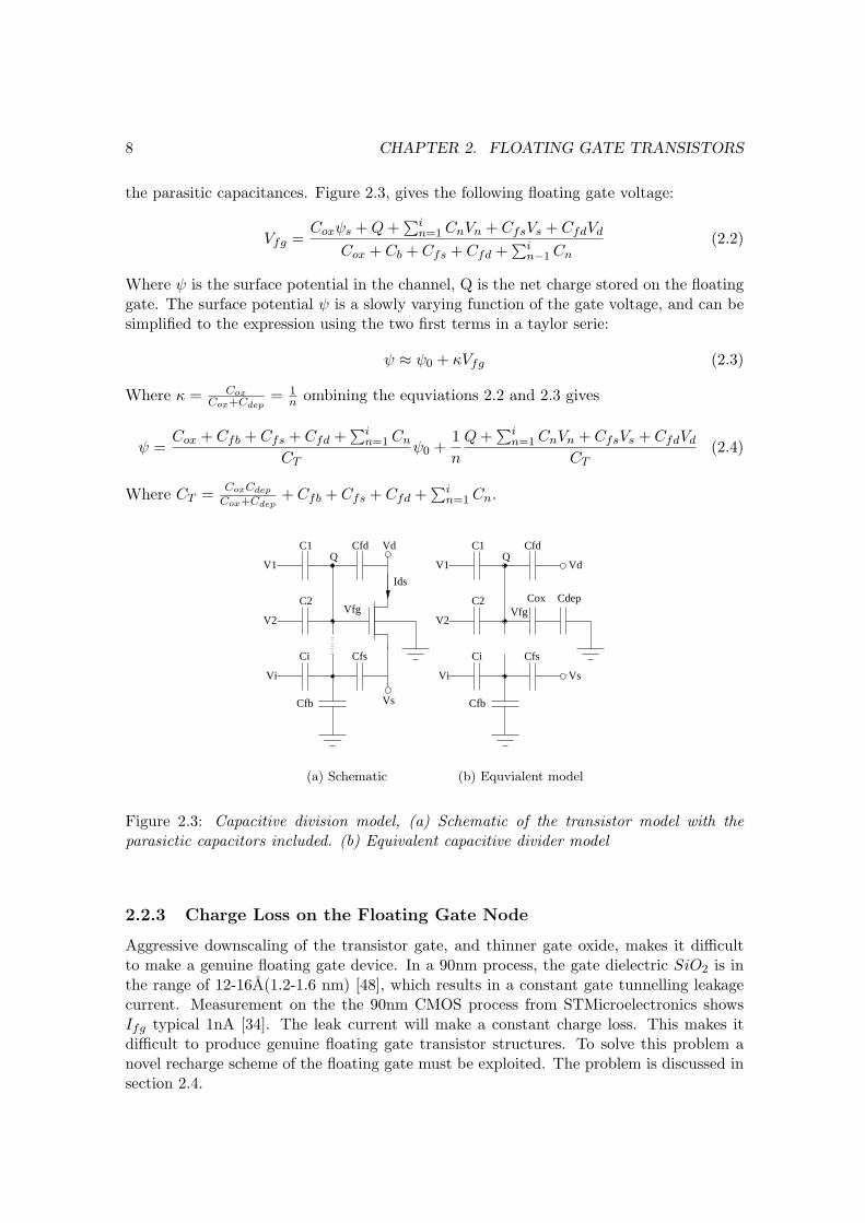
the parasitic capacitances. Figure 2.3, gives the following floating gate voltage:
Vfg =Coxψs +Q+
∑in=1CnVn + CfsVs + CfdVd
Cox + Cb + Cfs + Cfd +∑i
n−1Cn
(2.2)
Where ψ is the surface potential in the channel, Q is the net charge stored on the floatinggate. The surface potential ψ is a slowly varying function of the gate voltage, and can besimplified to the expression using the two first terms in a taylor serie:
ψ ≈ ψ0 + κVfg (2.3)
Where κ = Cox
Cox+Cdep= 1
nombining the equviations 2.2 and 2.3 gives
ψ =Cox + Cfb + Cfs + Cfd +
∑in=1Cn
CT
ψ0 +1
n
Q+∑i
n=1CnVn + CfsVs + CfdVd
CT
(2.4)
Where CT =CoxCdep
Cox+Cdep+ Cfb + Cfs + Cfd +
∑in=1Cn.
Vi
V1
C1
Ci
Cfd
Cfs
VfgV2
C2
Ids
Vd
VsCfb
Q
(a) Schematic
Vi
V1
C1
Ci
Vfg
Cfd
Vs
Cfs
Cox Cdep
Vd
V2
C2
Cfb
Q
(b) Equvialent model
Figure 2.3: Capacitive division model, (a) Schematic of the transistor model with theparasictic capacitors included. (b) Equivalent capacitive divider model
2.2.3 Charge Loss on the Floating Gate Node
Aggressive downscaling of the transistor gate, and thinner gate oxide, makes it difficultto make a genuine floating gate device. In a 90nm process, the gate dielectric SiO2 is inthe range of 12-16A(1.2-1.6 nm) [48], which results in a constant gate tunnelling leakagecurrent. Measurement on the the 90nm CMOS process from STMicroelectronics showsIfg typical 1nA [34]. The leak current will make a constant charge loss. This makes itdifficult to produce genuine floating gate transistor structures. To solve this problem anovel recharge scheme of the floating gate must be exploited. The problem is discussed insection 2.4.

2.2. FLOATING GATE (FG) MOS TRANSISTOR 9
2.2.4 Inverter Based Structures
A traditional CMOS digital structure uses stacking of more than two transistors to makea logical port. By using the floating gate technology this is not necessary. All structuresuses height of two, a PMOS stacked on a NMOS. The functionality of the digital logic ismade by capacitive division.
2.2.5 Split-Gate Inverter Structure
A split gate inverter structure has a separate capacitor of both the NMOS- and the PMOStransistor as shown in figure 2.4 a). A split gate structure can use minimum length andwidth NMOS and PMOS transistors. By using an appropriate programming technique ofthe floating gate of the NMOS and PMOS transistor, it is possible to compensate for thedifferent βs of these transistors [13].
2.2.6 Common Gate Inverter Structure
A common gate structure has a common capacitor connected to both gates of the NMOSand the PMOS, as shown in figure 2.4 b). In a common gate structure the NMOS andPMOS has to be matched. In the STMicroelectronic 90nm process the PMOS has to be≈ 3.5 times the width of the NMOS, due to the mobilityfactor(µ) of electrons. It alsoreduces the area needed for the capacitors, compared to a split-gate structure.
V V IN OUT
C
C
ip
in
(a) Split gate inverterstructure
V V IN OUT
Ci
(b) Common gate inverterstructure
Figure 2.4: Gate structures used in FG technology

10 CHAPTER 2. FLOATING GATE TRANSISTORS
2.3 Non-Volatile FG Transistors
Floating gate transistors need a programming technique to control the charge of the float-ing gate. Non-Volatile FG or genuine Floating Gates [51] are structures where the gateare only connected to capacitors, as mentioned in section 2.2.3. In newer CMOS technol-ogy with thin gate oxide, SiO2, there is a constant gate tunnelling current leakage, whichmakes it difficult to make a Non-Volatile FG structure. To solve this problem the gateoxide has to be a high resistance material (High-k dielectric), or it is possible to use anolder CMOS process technology.
In 2004, Intel demonstrated a 0.8 nm physical SiO2 in their research laboratory. Al-though transistors with the 0.8 nm gate oxide still show the expected device characteristics,the gate dielectric has become so thin that we are literally running out of atoms for furtherscaling [16].
2.3.1 Fowler Nordheim Tunneling
Fowler Nordheim tunnelling is a post programming process for FG structures. It is a wellknown method for a charge transport through the silicon dioxide. This technique wasdiscovered as early as 1928 when researchers Ralph H. Fowler and Lothar W. Nordheim,who gave the name to this method, discovered that electrons with sufficient electronic fieldcan tunnel through an energy barrier [22]. This method makes it possible to program theFG. However, as a result of the high voltage required, the SiO2 will gradually break down,resulting in leakage through the dioxide.
2.3.2 Hot Carrier Injection
Hot carrier injection, or hot-electron injection, is another method for controlling the chargeof the floating gate. Hot carrier injection is the phenomenon in solid state devices orsemiconductors where either an electron, or a ”hole”, gains sufficient kinetic energy toovercome a potential barrier, resulting in a ”hot carrier”, and then migrates to a differentarea of the device [19]. The term usually refers to the effect in a MOSFET where a carrieris injected from the silicon substrate to the gate dielectric. For a SiO2 dielectric, to enterthe conduction band of the dielectric, an electron must gain a kinetic energy of 3.3eV .
2.3.3 UV Activated Programming
UV Activated Programming is a method explored at the university of Oslo in 1996 [47].The advantage of the UV-activated mechanism is that the programming can be donewithout any high voltage or a special CMOS process. The UV programming is discussedin detail in my master thesis [24], and by Snorre Aunet in his Dr. Scient thesis ”Real-timeReconfigurable Devices Implemented in UV-light Programmable Floating-Gate CMOS”[3].
2.4. VOLATILE FG CIRCUITS 11
2.4 Volatile FG Circuits
Floating gate circuits need to be initialized, either once initially or frequently. The onceand for all initialization is synonymous with programming. By recharging the floating gatefrequently, we avoid problems with any leakage currents and random or undesired distur-bance of the floating-gate charges. The reset or recharge scheme can be used to overcomesome problems associated with floating-gate circuit design [5]. Thin gate oxide in modernCMOS processes makes it almost impossible to make a genuine floating gate structure,because of the constant gate current leakage (as discussed in 2.2.3). Volatile Floating gatetransistors are not genuine floating gates, since the gate node is not completely isolated.There are several methods to maintain the charge on the floating gate node, pseudo, semi,recharged or a combination. The methods are discussed in the following section.
2.4.1 Recharged Floating Gate
Recharged floating gate is also known as switched or clocked floating gate transistors.This method was presented by Kotani et al. in 1998 [45]. It makes it easy to controlthe charge on the floating gate. However, the transmission gate used for the clockingintroduces a constant leakage current. This makes the circuit more suitable to be used indigital applications, with sufficient clock frequency.
2.4.2 Pseudo Floating Gate
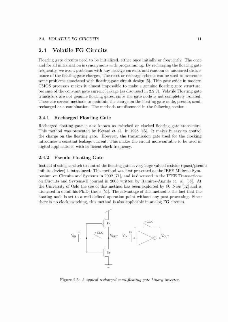
Instead of using a switch to control the floating gate, a very large valued resistor (quasi/pseudoinfinite device) is introduced. This method was first presented at the IEEE Midwest Sym-posium on Circuits and Systems in 2002 [71], and is discussed in the IEEE Transactionson Circuits and Systems-II journal in 2003 written by Ramirez-Angulo et. al. [58]. Atthe University of Oslo the use of this method has been exploited by Ø. Ness [52] and isdiscussed in detail his Ph.D. thesis [51]. The advantage of this method is the fact that thefloating node is set to a well defined operation point without any post-processing. Sincethere is no clock switching, this method is also applicable in analog FG circuits.
Ci
Ne
CiV V V
+ CLK
VININ OUTOUT+ CLK
Pe
Figure 2.5: A typical recharged semi-floating gate binary inverter.

12 CHAPTER 2. FLOATING GATE TRANSISTORS
2.4.3 Recharged Semi-Floating Gate
This recharge strategy is slightly different than the reset condition in clocked-Neuron-MOSlogic proposed by Kotani et.al. [45]. This is the reset scheme that is presented in thisPh.D. thesis. When resetting or recharging a gate, the inputs are recharged simultaneouslyand not set to a reference voltage, normally Vss or Vdd. By using a common gate inverterbased structure, figure 2.5, when being in recharge mode, the gates are short-circuited andthe output and the semi-floating-gate of a logic gate is forced to Vdd
2 . The recharge schemeis similar to biasing single-ended auto-zeroing comparators which have been used in high-speed flash AD converters. The main purpose of the recharge scheme is to initialize, orrecharge the semi-floating-gates, to an equilibrium state which can be utilized to yieldfast binary and multiple-valued signal processing. In addition, we may reduce the effectof mismatches, especially transistor mismatches, and power supply noise. The rechargescheme provides a simple, fast and accurate recharge to the equilibrium state for all gatesregardless of logical depth. We use the term Recharge Logic (RL) or Recharge Semi-Floating-Gate Logic (RSFGL) for the circuits used in this thesis [8]. The SFG circuits arerecharged to the initial equilibrium state, namely Vdd
2 .
A simple binary single input gate, namely an inverter, is shown in figure 2.5. Byequalizing the transfer parameters βn and βp of the N- and P-transistor, we obtain anequilibrium state when the recharge clock is 1. The output and gate are driven towardVdd
2 . When the recharge clock is 1, we have two distinct cases. Assuming that the input
signal is initially 1 (Vdd ), the SFG voltage can be expressed as (Vdd
2 ) x ( 1 + ki), whereki = Ci/Ct and Ct is the total capacitance seen by the SFG, and the output is equal to 0.The output and the SFG will be forced toward Vdd
2 simultaneously. The recharge current
which will pull the SFG down towards Vdd
2 , is larger than the equilibrium current (Ibec).We define the recharge rise time tr as the time required to recharge the output from 0 toVdd
2 (and the SFG simultaneously). If the input signal is initially 0 the SFG voltage is (Vdd
2) x (1 - ki) and the output is 1. The recharge current will be reduced compared to theformer case, due to body effect of the n-channel recharge transistor. In order to achieve acorrect recharge to the equilibrium state in a chain of gates, we need to recharge all gatesand all inputs simultaneously. Additionally, we need to develop a synchronization schemefor the recharge. We define the recharge fall time tf as the time required to recharge theoutput from 1 to Vdd
2 . The recharge frequency is twice the frequency of the input signal.
By recharging the semi-floating-gate (SFG) we do not only avoid the problems linkedto programming or initializing of the floating gates, instead we do convert the non-volatilefloating gates to semi-floating-gates. The control of the actual floating gate charges, interms of predictable long term charge restoration, becomes easier. The SFG is not influ-enced by a random FG charge distortion due to a periodic or frequent charge restorationor reset. The recharge of the SFGs is accomplished by a local recharge transistor or a passgate temporarily connecting the output to the floating gate of a gate [6].
2.4.4 Clock Generator
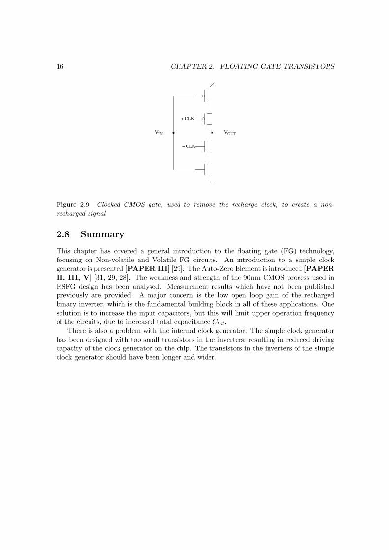
Recharged Semi Floating Gate circuits need a recharge scheme. This is the reason whywe need a clock generator to generate the refresh clock. An example of a simple clockgenerator is shown in figure 2.6. A simple clock generator can be made by using three

2.5. AUTO-ZERO ELEMENT 13
inverters [PAPER III] [29]. This simple clock generator generates the two clock phases+CLK and −CLK, the characteristics are shown in figure 2.7. The reference clock couldbe any periodic signal, for instance a sinus signal. The clock generator should have thedriving possibility of driving several circuits, and therefore the transistors have to be widerthan minimum.
REF − CLK
+ CLK
Figure 2.6: A simple clock generator.
2.5 Auto-Zero Element
The Auto-Zero element (AZE) can be seen as a signal converter [PAPER II, III, V] [31,29, 28]. By using the AZE we are able to use DC signals in addition to a conventionalbinary signal as input to the FG circuits. When interfacing with a binary signal the clockfrequency has to be twice the input frequency of the binary signal. Examples of auto-zeroelements are seen in figure 2.8. Figure 2.8 (a) consists of two pass gate circuits which isopposite clocked. The upper has Vdd
2 as input, the lower Pass Gate circuit has the inputsignal Vin as input.
Measured typical output characteristics of the circuit in figure 2.8 (a) is presentedin figure 2.10 and figure 2.11. The discussion of the results is focused in section 2.7.Figure 2.8 (b) shows another solution. It has stacked transistors, resulting in limitationson use in very high frequency applications, due to body effect. The N and P transistors(diode coupled) connected to the rails need to have matched transfer parameters (βn andβp). The two solutions uses an equal amount of transistors, because the Vdd
2 input on a)is made using a diode coupled N and P transistor.
2.5.1 Removing the Auto-Zero Clock Signal
When interfaced with other logic components, which is not RSFG compliable, we needto remove the recharge clock. This can be done using a recharge-remover as shown infigure 2.9. This makes it simple to implement the RSFG circuits in any logic design.
2.6 Limitations Using 90nm CMOS Technology
2.6.1 Max Clock Frequency
The simulation result I have done of the 90nm CMOS process from STMicroelectronicsshows that switching at ≈ 10GHz of binary inverters is possible to achieve. However, dueto total load capacitance of the FG devices, the frequency of the presented RSFG circuitsin this thesis is limited to MAX 2GHz. The applications used in this thesis are designedfor 1GHz switching frequency at a load of 10fF.

14 CHAPTER 2. FLOATING GATE TRANSISTORS
0 0.2 0.4 0.6 0.8 1 1.2 1.4 1.6 1.8
x 10−8
−0.5
0
0.5R
EF
0 0.2 0.4 0.6 0.8 1 1.2 1.4 1.6 1.8
x 10−8
−0.5
0
0.5
− C
LK
0 0.2 0.4 0.6 0.8 1 1.2 1.4 1.6 1.8
x 10−8
−0.5
0
0.5
+ C
LK
Figure 2.7: Characteristics of the simple clock generator implemented in 90nm CMOStechnology, the reference clock is 1 GHz
2.6.2 Parasitic Capacitance
When designing a MOS Transistor in a VLSI design, there are many non-desirable effectsto consider. One of these effects is the parasitic capacitance. Most of this effect is takeninto consideration in the different simulation models (ie. BSIM3 Spice models).
There are major parasitic capacitances between metal layers, so thoroughly routing isof significant value. In the CMOS transistor itself, the most dominant parasitic capacitanceis the gate capacitance Cgtot = Cgd + Cgs, in the 90nm this is in a order of ≈ 1fF. Thismeans that the input capacitor (Ci) of the FG circuit, has to be more than Cgtot. Theother overlap capacitance Cdb + Csb << Cgtot, are not taken into consideration in thissimple model.
2.6.3 Gate Leakage in Thin Oxide Layers
As mentioned in section 2.2.3 the Ileak ≈ 1nA for a static FG circuit using low voltagethreshold (LVT) transistors. The circuits are designed to operate at clock frequency of 1GHz, and by using this clock rate the gate leakage will be minimal, resulting in the factthat this will not be an issue for a possible failure for these circuits.

2.7. MEASUREMENT AND RESULTS 15
!
"# $%
&'()
*+,-
. ./ /
01
2345
67
89
+ CLK
V
− CLK VV V
VIN
INOUT OUT
− CLK
+ CLK
+ CLK
DD/2
b)a)
Figure 2.8: Typical auto-zero elements
2.7 Measurement and Results
Measured typical output characteristics of the auto-zero circuit in figure 2.8 (a) is presentedin figure 2.10 and figure 2.11. Yellow signifies the clock signal (1Vpp), blue is the outputsignal. The input signals are DC-signals at 100mV (a), 900mV (b) and 500mV (c). Theclock frequency is 200 KHz. This shows a typical recharge signal, with three significantlevels. The refresh or recharge period represents the period when the clock-pulse is high,the evaluation period is when the clock-pulse is set low.
2.7.1 Gain
Figure 2.12 shows the measured DC characteristics of a SFG binary inverter shown infigure 2.5, using a 90nm CMOS process from STMicroelectronics. The DC-gain ADC is≈ −1. The DC characteristic is interpolated from the recharge signal measured on theoscilloscope showed in figure 2.13. The recharge clock has a frequency of 200 KHz. Toincrease the gain, the input metal-to-metal capacitors should perhaps have been largerthan ≈ 1Ff as they are today. The result should not been a reduction of the input signalby the same amount, and could have increased the open loop gain of the circuit. Byincreasing the capacitors, the compactness of the design is reduced. To compensate forthis fact, stacking of capacitors using several metal layers has to be introduced.
16 CHAPTER 2. FLOATING GATE TRANSISTORS
:; <=V VIN OUT
− CLK
+ CLK
Figure 2.9: Clocked CMOS gate, used to remove the recharge clock, to create a non-recharged signal
2.8 Summary
This chapter has covered a general introduction to the floating gate (FG) technology,focusing on Non-volatile and Volatile FG circuits. An introduction to a simple clockgenerator is presented [PAPER III] [29]. The Auto-Zero Element is introduced [PAPERII, III, V] [31, 29, 28]. The weakness and strength of the 90nm CMOS process used inRSFG design has been analysed. Measurement results which have not been publishedpreviously are provided. A major concern is the low open loop gain of the rechargedbinary inverter, which is the fundamental building block in all of these applications. Onesolution is to increase the input capacitors, but this will limit upper operation frequencyof the circuits, due to increased total capacitance Ctot.
There is also a problem with the internal clock generator. The simple clock generatorhas been designed with too small transistors in the inverters; resulting in reduced drivingcapacity of the clock generator on the chip. The transistors in the inverters of the simpleclock generator should have been longer and wider.

2.8. SUMMARY 17
(a) Input −1 (100mV DC) (b) Input +1 (900mV DC)
Figure 2.10: Measured output characteristics of the auto-zero element in figure 2.8(a) withinput signals -1 and +1
(a) Input +0 (500mV DC)
Figure 2.11: Measured output characteristics of the auto-zero element in figure 2.8(a) withinput signal +0
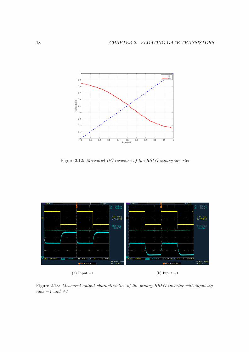
18 CHAPTER 2. FLOATING GATE TRANSISTORS
0 0.1 0.2 0.3 0.4 0.5 0.6 0.7 0.8 0.9 10
0.1
0.2
0.3
0.4
0.5
0.6
0.7
0.8
0.9
1
Input (volt)
Out
put (
volt)
InOut
Figure 2.12: Measured DC response of the RSFG binary inverter
(a) Input −1 (b) Input +1
Figure 2.13: Measured output characteristics of the binary RSFG inverter with input sig-nals −1 and +1

Chapter 3
MULTIPLE-VALUEDTECHNOLOGY
”If some day multiple-valued gates were introduced to practical applications, themarkets for them will be so large that it will stimulate exponential growth ofresearch and development in multiple-valued logic, and then, the accumulated50 years of research in multiple-valued logic will prove to be very practical.”
- Marek Perkowski
3.1 Introduction
Multiple-valued logic (MVL) has in the last few decades been proposed as a possiblesubstitute of binary logic. While binary logic is limited to only two states, ”true” or”false”, multiple-valued logic (MVL) can replace these with finitely or infinitely numbersof values. A MVL system is defined as a system operating on a higher radix than two[67]. A radix-n set has n elements, 0, 1...n− 1. The practicability of MVL depends onthe accessibility of the devices constructed for MVL operations [20]. The devices shouldbe able to switch between the different logical levels, and preferably be less complex thanthe binary counterparts. Today there are not yet any reliable commercial circuits usingMVL technology. Mostly all of the VLSI companies have invested a lot of money intobinary technology even though it is almost impossible to shrink the transistors indefinitely.According to the ITRS1 we will face the brick wall in 2015 if we continues in the samedevelopment speed. So we have to come up with other solutions, and MVL is one of mostpromising one. MVL can in principle increase data processing capability per unit chiparea in the future.
Many m-valued circuits have been presented but not that many have been successful.This is an issue covered by D. Etiemble [21]. Usually, m-valued designs make complexsolutions, while floating gate structures makes m-valued circuits less complex. This is apoint to remember. It is true that the noise margins are a serious issue, which is the reasonwhy my solutions are ternary. This will keep the noise margins at an acceptable level. In2004, a research team in Rennes made a MVL Chip using SUpplementary Symmetrical
1International Technology Roadmap for Semiconductors
19

20 CHAPTER 3. MULTIPLE-VALUED TECHNOLOGY
LOgic Circuit structure (SUS-LOC). A 64-tert SRAM and a 4-tert adder was made [56].This was the very first full-ternary circuit ever fabricated successfully. This technologylead to the establishment of a company named Omnibase Logic2, which mainly focuseson using MVL logic in digital circuit design. The company is situated in Austin, Texas.Omnibase Logic received the World Economic Forum 2007 Technology Pioneer Award inDecember 2006 due to innovative use of new technology. The Omnibase Logic’s selectedpublications are presented in the following papers [53, 55, 43, 1, 54]
3.1.1 History
The history of Multi-Valued Logic as a separate topic began in the early 1920s by Polishphilosopher Jan Lukasiewicz (1878-1956) [46]. His objective was to introduce a third addi-tional truth-value for ”possible”. The outcome of this research is known as the Lukasiewiczsystems or the ternary predicate calculus. Parallel to the approach of Lukasiewicz, theAmerican mathematician Dr. Emil Leon Post (1897-1954), born in Bialystok in Poland,introduced the idea of several additional truth degrees, and used this approach to solvethe problem of the represent ability of functions, also known as the Post Algebra[17].
3.2 Multiple-Valued Logic
3.2.1 Notation
The radix (r) defines the number of logic levels used in a multiple-valued numberingsystem. A high radix gives a more complex computation, and a higher amount of possiblelogic functions. A multiple-valued numbering system which has a continuous monotonicset of integers, given as 0, 1...r, is called an unbalanced system (or unsigned system).The binary numbering system is a subset of this continuous set of integers 0, 1. Abalanced numbering system uses odd radixes and includes negative numbers, which givesa monotonic set of integers − r−1
2 ..., 0, ... r−12 . A balanced ternary numbering system will
then be specified by −1, 0,+1. The advantages using a balanced ternary numberingsystem will be covered in more detail in Chapter 4.
3.2.2 Radix and Complexity
A general operand with two inputs called A and B, and one output called F (see equa-tion 3.1), can form different functions. This gives for a binary system 22∗2 = 16 logicfunctions, a two-input ternary operands with one output can form (33∗3)= 19683 possiblelogic functions.
F (max(A)∗max(B)) (3.1)
Higher radixes lead to more complexity, but is there an optimal radix? If we look at ther ∗ w product, where r is the radix and w is the width of the word, this product hasbeen said to reflect a good estimate for an optimal hardware complexity. The derivationof the function r ∗ w gives a minimum for r=2.71828, the radix and width is treated as
2http://www.omnibaselogic.com
3.2. MULTIPLE-VALUED LOGIC 21
continuous variables. This is remarkably the napierian base3 [2]. The minimum is closerto radix 3 than to radix 2, hence base 3 is the most optimal numbering system. Hereis an example for the r ∗ w product for the decimal number 1024. By using the decimalnumbering system with radix=10, the r ∗ w product is given as 10 ∗ 4 = 40, binary withradix=2 (10000000000) gives 2∗11 = 22, ternary with radix=3 (1101221) gives 3∗7 = 21.
3.2.3 Modes of Operation
There are several ways to represent a discrete signal. For instance as voltage, current,charge or frequency. In the binary world the most used representation is voltage mode,due to the use of devices with natural two-state behaviours, e.g. the MOSFET transistor.In MVL it is not obvious which mode of operation is preferred; there are mainly two modesof operation; current- and respectively voltage-mode.
Current mode
In MVL current mode, the logic levels are multiples of a base current, and can be imple-mented using current mirrors. Addition can be implemented even simpler just by con-necting two wires. This makes it very area cost efficient. There are two major problemswith current mode operation, delay and frequency response [7].
Voltage mode
In voltage mode the discrete levels are set by the threshold voltages. Voltage mode isonly suitable for low radix operations due to low noise margins for high radixes and inaddition to make sure that the design is robust enough. Voltage mode may suffer from thesame problems as current mode, however it is easier to implement a signal independentfrequency response by using voltage mode [7]. The applications presented in this thesisare voltage mode circuits.
3.2.4 Noise Margins
In the binary world, the noise margin is the amount of which a signal exceeds the thresholdfor a proper ’0’ or ’1’. In the MVL world the signal can be in the range from ’0’....’r ’,where r is the radix, hence it has a reduced noise margin with increased radix. Let usassume an example in the use of ternary logic (’0’, ’1’ or ’2’) in a voltage mode application.Suppose the supply voltage is 1 Volt, with a 25% noise margin, this will give a valid signalfor ’0’ in the range of 0...250mV, ’1’ from 375mV..625mV and ’2’ from 750mV..1V, andundefined in the range of 251mV..374mV and 626mV..749mV.
3.2.5 Completeness
In logic, completeness is when all tautologies4 are theorems. Kurt Godel (1906-1978), LeonHenkin (1921-2006) and Emil L. Post (1897-1954) all published proofs of completeness.
3Named after the Scottish mathematician John Napier (1550-1671), he developed the concept of thelogarithm and also effectively introduced the modern notation of decimal fractions
4Tautology, a statement of propositional logic which can be inferred from any proposition whatsoever

22 CHAPTER 3. MULTIPLE-VALUED TECHNOLOGY
Henkin’s result was not novel; the completeness theorem had initially been proved by KurtGodel in his doctoral dissertation which was completed in 1929, Godel also published aversion of the proof in 1930. Henkin’s 1949 proof is easier to follow than Godel’s and hasthus become the standard choice of completeness proof for presentation in introductoryclasses and texts. The Post-algebra developed by Emil L. Post in 1929 also satisfied theproof of completeness. In 1965 and 1970 Ivo Rosenberg published the general conditionsfor a complete MVL logic [59, 60].
3.2.6 MVL-Inverter
A MVL inverter is a complement function; which in the binary notation is known as aninverter. In this thesis I label it the MVL-NOT function. As an example I will use aternary signal, x. The rule of ’ternary inversion’ is shown in table 3.1. A MVL-NOTfunction is an elementary function in MVL, and it is commonly used in nearly all of myapplications proposed in this thesis.
Table 3.1: The rule of ’ternary inversion’
x 0 1 2
x 2 1 0
An analog inverter is an useful application for realization of the NOT function in multi-valued logic [38]. In order to make a voltage mode multi-valued signal, high accuracy isnecessary, hence high linearity, because the voltage levels for each logic level are an equaldivision of Vdd. That is the reason why the analog inverter is a key element in MVL.The MVL Inverter is based on a low voltage amplifier presented in my master thesis andjournal papers [24, 11, 13]. It is based on an analog amplifier with voltage gain of −1.It is called an analog inverter because of the output characteristic. The analog amplifierwas a split gate FG circuit; however, the proposed circuits in this thesis are common gateFG circuits. A split gate FG has a capacitor connected to each of the gates on the n-and p-transistor [51]. A common gate has one capacitor connected to both gates of then- and p-transistor (figure 3.1). The theory behind is the same and is covered in detail inmy master thesis [24]. The SFG Recharged MVL Inverter is shown in figure 3.1. It hasa weighted negative feedback mechanism (Cf ), and ideally the gain is −1. The transfercharacteristic of the analog inverter, which is given by Eq. 3.2, is determined by capacitivedivision factors ki and kf ( ki = Ci
Ctotaland kf =
Cf
Ctotal).
Vout = Vdd − Vin (3.2)
Where Vin and Vout are the voltages on the input and output terminals, Vdd is the supplyvoltage.

3.2. MULTIPLE-VALUED LOGIC 23
The voltage gain is determined by the relationship between, Ci and Cf . The voltage gainof this circuit is given by equation 3.3. Ideally Ci = Cf , while in practice Cf has to beslightly smaller than Ci due to the output conductance and the parasitic capacitance, Cgd
[11].Measurement and analyeses of the MVL-inverter is presented in section 3.3.
Av =∆Vout
∆Vin=Ci
Cf
(3.3)
>?
@A BC
DEFGHI
JKL LMN NOP PQ
Pe
Ne
ViC
V
fC
+ CLK
V
C i
+ CLK
C f VVsfgVsfg
OUT OUTININ
Figure 3.1: A typical RSFG MVL Inverter
3.2.7 Logic Operations
In binary logic the most fundamental logic functions are ”AND”, ”OR” and ”NOT”, thecorresponding functions in MVL logic is called ”MIN”, ”MAX” and ”NOT”. A MINfunction gives the minimum value of the input signal x. Where x ∈ 0, 1, 2, .., r − 1, ris the radix of the signal. Table 3.2 shows the truth table of a two input ternary MINfunction. A MAX function gives the maximum value of the input signal x, and table3.3 shows the truth table of this function. It can easily be proven that the binary ANDfunction is actually a MIN function, and the binary OR is a MAX function. The NOTfunction is explained in section 3.2.6. MVL logic introduces a vast array of new functions,but will not necessarily be useful in all the terms of functionalities.
3.2.8 Down Literal Circuits
One of the most important functions in MVL is the Down-Literal Function. Which divideslogic levels in the multi-valued logic into a binary state at an arbitrary threshold [PAPERI, II][26, 31, 35, 37, 36, 62]. A Down Literal Circuit (DLC) is said to be a binary inverterwith a multi-valued input and a threshold [70]. The function of a DLC Dj(x) is given byEq. 3.4. It outputs r − 1 if x is equal or less to the threshold j, else the output is zero.
Dj(x) = r−1 (x≤j)
0 (x≥j+1) (3.4)

24 CHAPTER 3. MULTIPLE-VALUED TECHNOLOGY
Table 3.2: The ternary MIN function
x · y 0 1 2
0 0 0 0
1 0 1 1
2 0 1 2
Table 3.3: The ternary MAX function
x+ y 0 1 2
0 0 1 2
1 1 1 2
2 2 2 2
Where x ∈ 0, 1, 2, .., r − 1 and j ∈ 0, 1, 2, .., r − 2, and r is the Radix of the signal.
The proposed DLC is implemented with Recharged Semi Floating Gate Transistors (Fig-ure 3.2). The DLC is made with n- and p transistor iwith equalized transfer parametersβn and βp, and with two capacitors Ci1 and Ci2. By changing the size of Ci1 and Ci2, itis possible to change the switching point between Vin1 and Vin2. The threshold voltage ofthe DLC is depended of the capacitive voltage division of the input voltage on Ci1 andCi2. The functionality is explained in the published papers.
3.2.9 Pass Gate Circuits
A pass gate (PG) network is commonly used to help realizing a MVL function in MVLhardware [61]. I use it in the MAX and MIN circuits proposed in section 3.2.11. Therecharge clock used in the recharge scheme is also implemented using a PG network.
3.2.10 Voltage Comparators
By combining the analog (MVL) inverter and the DLC circuit, it is possible to make avoltage comparator which can be seen in figure 3.4 and 3.3 [PAPER I], [26, 38]. Thevoltage comparator is the heart of the MAX and MIN circuits presented in the previoussection. A SFG voltage comparator with a removal of the interleaved recharge voltage ispresented by Jensen et al. [40]. This is useful if it is desirable to have a selection signalwhich is valid over several clock periods.

3.2. MULTIPLE-VALUED LOGIC 25
R RST TUV VW
X XY
Z Z[ [\ \] ] ^ _
Pe
V
VV
VIN1
IN2
OUT
IN1V
IN2VOUTsfgV sfgV
i2C
Ci1
i2C
Ci1
Ne
+ CLK
+ CLK
Figure 3.2: A down literal circuit
C4
C5
nPG
pPG
C1
C2 C3
+ CLK+ CLK+ CLK
BINOUT
INPUT 2
INPUT 1
OUTPUT
MVL INVERTER DLC
VOLTAGE COMPARATOR
abc
defghijk
lmno pq rs
tu
vw
xy
Figure 3.3: A RSFG MAX circuit
3.2.11 Max and Min Functions
MAX and MIN functions are fundamental functions in MVL [PAPER I], [37, 36]. TheMAX and MIN functions have been implemented using Neuron-MOS Transistors in float-ing gate technology [38, 36, 37]. However, another way of realizing these functions is byusing recharged SFG logic. This makes it possible to implement a low-power digital systemwith reduced dynamic power dissipation, without any post-production of the chips. Theadvantage of this technology is presented in [5] and the circuits are presented in figure 3.3and figure 3.4. As these figures shows; the MIN- and the MAX-circuit uses an analog(MVL) inverter and a DLC to make a voltage comparator. The output of the voltagecomparator gives a selection signal to the pass gate circuitry, which consists of a pPass-Gate (pPG), a nPassGate (nPG) and an inverter. The pPG lets the signal through whenthe output of the comparator is ”0”, and the nPG lets the signal pass when the output ofthe comparator is ”1”. To obtain a MIN function, the nPG can swap place with the pPG;
26 CHAPTER 3. MULTIPLE-VALUED TECHNOLOGY
C4
C5
pPG
nPG
C1
C2 C3
+ CLK+ CLK+ CLK
BINOUT
INPUT 2
INPUT 1
OUTPUT
MVL INVERTER DLC
VOLTAGE COMPARATOR
z|~
Figure 3.4: A RSFG MIN circuit
0 0.1 0.2 0.3 0.4 0.5 0.6 0.7 0.8 0.9 10
0.1
0.2
0.3
0.4
0.5
0.6
0.7
0.8
0.9
1
Input (volt)
Out
put (
volt)
InOut
Figure 3.5: Measured DC response of a RSFG MVL inverter in 90nm CMOS technology
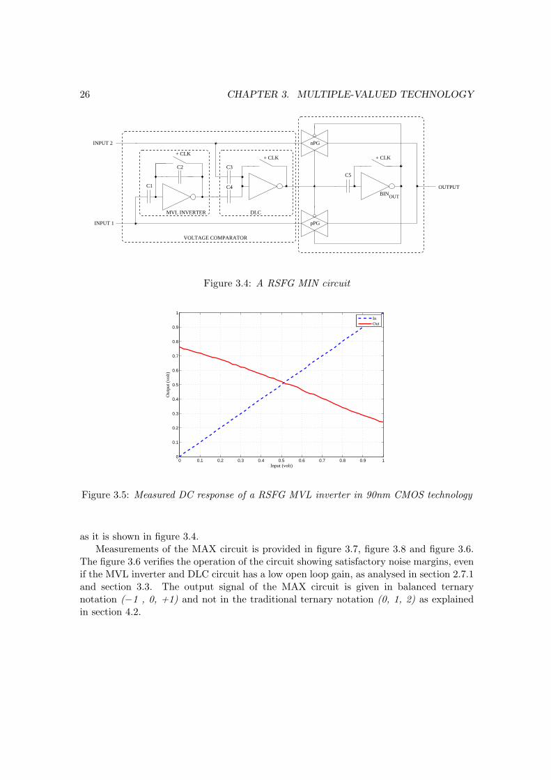
as it is shown in figure 3.4.Measurements of the MAX circuit is provided in figure 3.7, figure 3.8 and figure 3.6.
The figure 3.6 verifies the operation of the circuit showing satisfactory noise margins, evenif the MVL inverter and DLC circuit has a low open loop gain, as analysed in section 2.7.1and section 3.3. The output signal of the MAX circuit is given in balanced ternarynotation (−1 , 0, +1) and not in the traditional ternary notation (0, 1, 2) as explainedin section 4.2.

3.3. MEASUREMENT AND RESULTS 27
−1 −1 −1 0 0 0 +1 +1 +10
0.5
1
INP
UT
1
−1 0 +1 −1 0 +1 −1 0 +10
0.5
1
INP
UT
2
−1 0 +1 0 0 +1 +1 +1 +1"−1"
"0"
"+1"
OU
TP
UT
Figure 3.6: Measured output charcteristics of the RSFG MAX-circuit
3.3 Measurement and Results
A measurement of the MVL inverter is shown in figure 3.9, figure 3.10 and figure 3.5. Themeasurements are done in a 90nm CMOS process supported by STMicroelectonics. If wedo analyze the result in figure 3.5, we can observe the gain A=−0.6, which is significantlyless than −1. In Chapter 2 the inverter gain of this process using SFG inverter structurewas analyzed. The open loop gain, AO was found to be −1. The feedback capacitor Cf
reduces the gain. The capacitive division factor is set correctly, however the internal openloop gain of the inverter is too low, which causes the problem. Measurement of the MVLinverter is not satisfactory; however the MAX circuit is still functioning properly, evenif the MVL inverter has narrow noise margins. This makes it difficult to maintain logicdepths. This issue is discussed in 2.7.1.
3.4 Summary
This chapter has covered a short introduction of the fundamentals of MVL logic. Somenew and interesting SFG circuit solutions in 90nm has been presented, including a MVL-NOT, a MAX, a MIN, and a DLC circuit [PAPER I, II] [26, 31]. These fundamentalfunctions make it possible to design several interesting MVL circuits that can be used inan ALU. Measured characteristics of the MVL-NOT and the MAX circuit are provided,showing the potential of recharged SFG circuits.
28 CHAPTER 3. MULTIPLE-VALUED TECHNOLOGY
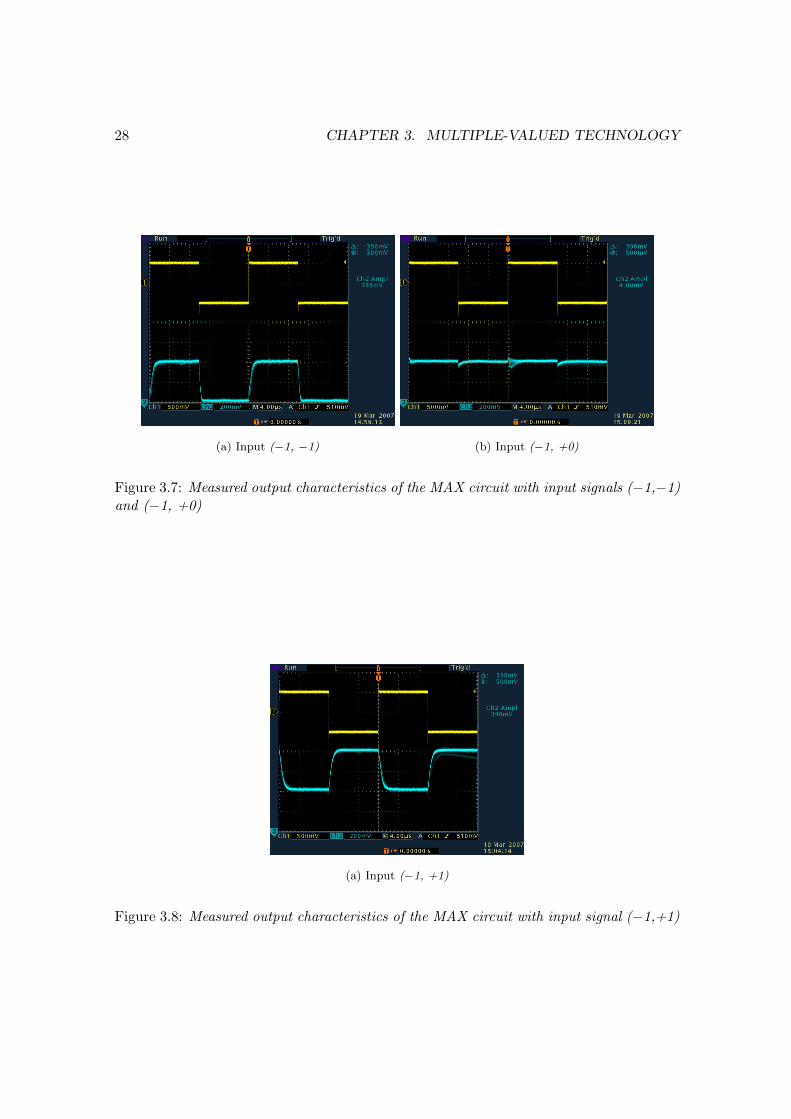
(a) Input (−1, −1) (b) Input (−1, +0)
Figure 3.7: Measured output characteristics of the MAX circuit with input signals (−1,−1)and (−1, +0)
(a) Input (−1, +1)
Figure 3.8: Measured output characteristics of the MAX circuit with input signal (−1,+1)

3.4. SUMMARY 29
(a) Input +1 (900mV) (b) Input −1 (100mV)
Figure 3.9: Measured output characteristics of a RSFG MVL inverter in 90nm CMOStechnology with input signal +1 and −1
(a) Input +0 (500mV)
Figure 3.10: Measured output characteristics of a RSFG MVL inverter in 90nm CMOStechnology with input signal +0

30 CHAPTER 3. MULTIPLE-VALUED TECHNOLOGY

Chapter 4
TERNARY LOGIC
”Multiple-valued logic allows us to do things that are not possible in binary logicand we can achieve them in many more ways than in binary. Multiple-valuedlogic functions can be very useful in applications such as line-coding, data-scrambling, sequence generation for wireless applications, arithmetical engines,and for what probably would be called digital control and Multiple-valued logiccombinational applications.”
- Peter Lablans, Ternarylogic.com, 2007
4.1 Introduction
Ternary logic is MVL compliant. However, only three logic states are used, ”0”,”1” and”2”. As mentioned in section 3.2.2, the optimum radix (r) of a fractional number is foundto be the natural logarithm (e). Ternary logic uses number representation with r=3,compared to binary logic witch uses r=2, hence the most economical integer radix whichis the closest to the natural logarithm e, is base 3 [32]. This special property of base 3inspired the early computer designers to build a ternary computer. The first approach tobuild an electronic MV-computer with ternary architecture was in the early 50 in USA. Theearliest published discussion focusing ternary logic, appears in the 1950 book High-SpeedComputing Devices, a survey of computer technologies compiled on behalf of the U.S Navy,by the staff of Engineering Research Associates [39]. However, the first working ternarycomputer was built in Russia at the Moscow State University in 1958. The computer wasdesigned by Nikolai P. Brusentow and his colleagues. They named it Setun, like the riverthat flows near the university campus [14]. From 1958 to 1965 around 50 machines wherebuilt. The idea of building a MVL computer is not dead, currently a company situated inUSA, Ternarylogic LLC1, owns several patents used in MVL- and ternary logic.
1http://www.ternarylogic.com
31

32 CHAPTER 4. TERNARY LOGIC
4.2 The Balanced Ternary Numbering System
Today, mostly all hardware is designed for binary computing. If we have had a stableelectronic component with three stable states, the world perhaps would have turned toternary computing. However this is not the truth today. Still I do claim there would bean advantage if we where using the balanced ternary numbering systems by using RSFGlogic.
Balanced ternary is a non-standard positional numeral system (a balanced form), usefulfor comparison logic. It is a ternary system, however unlike the standard (unbalanced)ternary system, the digits have the values −1, 0, and +1. This combination is especiallyvaluable for ordinal relationship between two values, where the three possible relationshipare less-than, equal-to, and greater-than. This will be discussed in section 4.3.1. Balancedternary can represent all integers without resorting to a separate minus sign.
The balanced ternary numbering system uses radix 3 hence the digits weights arepowers of three: 27, 9, 3, 1, 1/3, 1/9, 1/27, while the digit values are −1, 0 and +1.Balanced ternary numbers are also known as Signed-Digit Numbers [57]. The so-called’Brousentsov’s Ternary Principle’ of computer design was initially realized in the Setuncomputer [69] and this computer was based on the ’Ternary-symmetrical number system’,which is another name for the balanced ternary notation.
As early as 1840, Thomas Fowler, a self-taught English mathematician, invented aternary mechanical calculating machine which used balanced ternary notation. All detailson the calculating machine were lost, until recently. A research project, initialized in1997, has managed to gather all the information which was needed to re-create a workinghistorical replica [23]. Fowler used the terms −, 0 and + for a negative, a zero and apositive number. The terms which is used in my thesis are −1, 0 and 1.
A balanced ternary number 1 0 −1 −1 (2310), is interpreted as: 1x33 + 0x32 − 1x31 −1x30, or 27+0−3−1=23, in decimal notation.
The balanced ternary radix notation has some beneficial properties:a) ’Ternary inversion’ [69] is easy, just change −1 with 1, and vice versa. If we use theexample −23, the result will be −1 0 1 1 in balanced ternary notation. This is simplerthan the rule for the two’s complement in binary logic.b) The sign of a number is given by its most significant nonzero ’trit2’c) The operation of rounding to the nearest integer is identical to truncation.d) Addition and subtraction are essentially the same operation; you merely add the digitsusing the rules for addition of digits.e) Carry occurs less often because only 2/9 of the possible digits sums results in carry,compared to 1/4 in binary. Carry ripples tend to be shorter in balanced ternary thanwhat is the case in a binary system, due to a zero result from a plus carry into a minusdigit or vice versa.
There have been several attempts to realize arithmetic applications by using the ternarynumbering system, but currently without any commercial success [33] [18].
2One trit has 3 values −1, 0, and 1, it is analogous to bit in the binary world (0 , 1).
4.3. SEARCH TREES USING BALANCED TERNARY NOTAION 33
4.3 Search Trees Using Balanced Ternary Notaion
The Ternary numbering system gives in theory the fastest search path in a tree structure.An example of a ternary structure is a telephone menu system, with eight choices. If youare using a binary structure, you will have two choices for each level. This gives us theperformance number of 4.53. A ternary structure, with three choices for each level, willhave a performance number of 3.75. This is the optimal number [32].
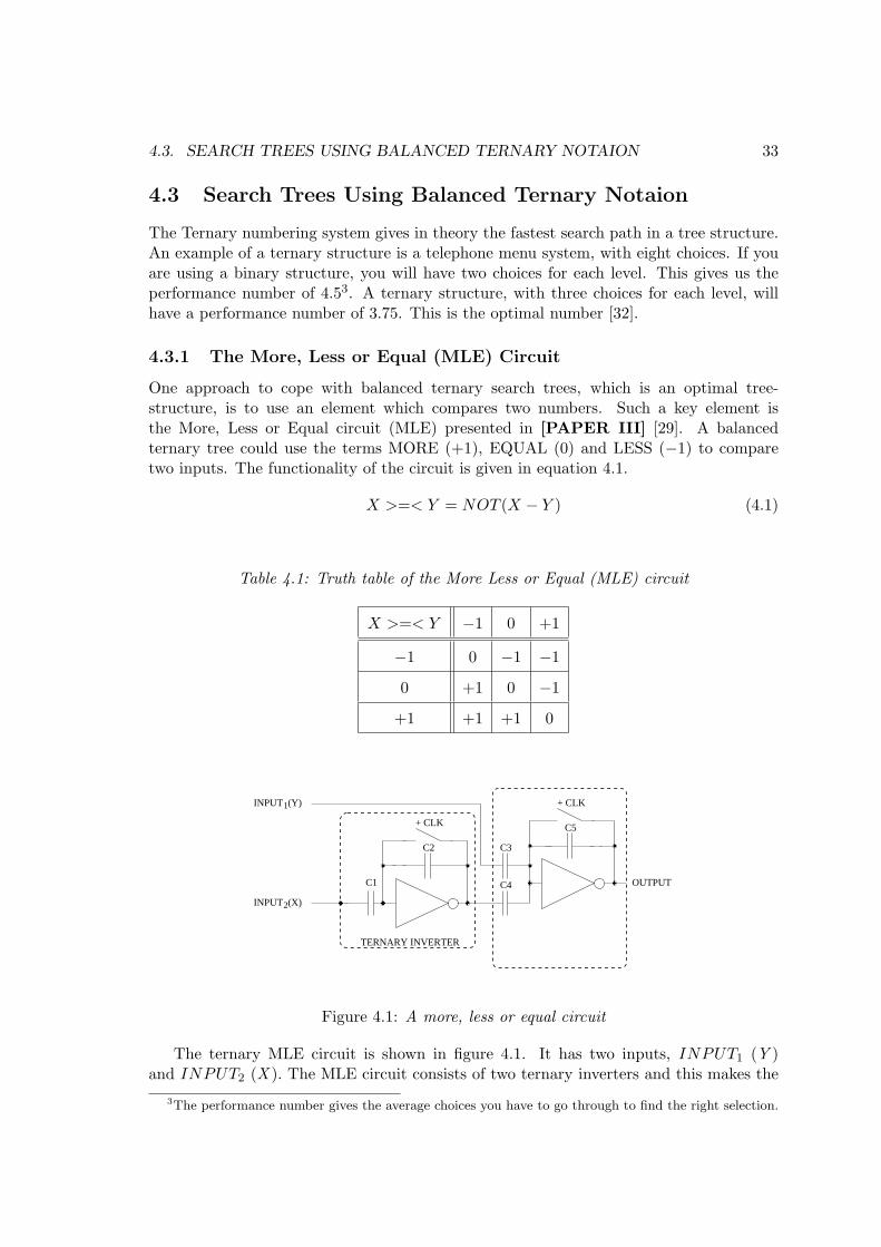
4.3.1 The More, Less or Equal (MLE) Circuit
One approach to cope with balanced ternary search trees, which is an optimal tree-structure, is to use an element which compares two numbers. Such a key element isthe More, Less or Equal circuit (MLE) presented in [PAPER III] [29]. A balancedternary tree could use the terms MORE (+1), EQUAL (0) and LESS (−1) to comparetwo inputs. The functionality of the circuit is given in equation 4.1.
X >=< Y = NOT (X − Y ) (4.1)
Table 4.1: Truth table of the More Less or Equal (MLE) circuit
X >=< Y −1 0 +1
−1 0 −1 −1
0 +1 0 −1
+1 +1 +1 0
C4
C5
C3
OUTPUTC1
C2
+ CLK
+ CLK
INPUT (X)2
1INPUT (Y)
TERNARY INVERTER
¡
¢£¤¥¦§
©
Figure 4.1: A more, less or equal circuit
The ternary MLE circuit is shown in figure 4.1. It has two inputs, INPUT1 (Y )and INPUT2 (X ). The MLE circuit consists of two ternary inverters and this makes the
3The performance number gives the average choices you have to go through to find the right selection.

34 CHAPTER 4. TERNARY LOGIC
0 0.2 0.4 0.6 0.8 1 1.2 1.4 1.6 1.8
x 10−8
−0.5
0
0.5IN
PU
T 1
0 0.2 0.4 0.6 0.8 1 1.2 1.4 1.6 1.8
x 10−8
−0.5
0
0.5
INP
UT
2
0 0.2 0.4 0.6 0.8 1 1.2 1.4 1.6 1.8
x 10−8
−0.5
0
0.5
INP
UT
2 IN
V
0 0.2 0.4 0.6 0.8 1 1.2 1.4 1.6 1.8
x 10−8
−0.5
0
0.5
OU
TP
UT
Figure 4.2: A typical output plot of the more, less or equality circuit
solution compact. A similar binary solution (the equality circuit) uses 2 inverters, 2 ANDgates and 1 OR gate, and it only tests for equality. The truth table of the MLE is shownin table 4.1. Figure 4.2 shows the typical characteristics of the circuit, while the measuredcharacteristic is supported in figure 4.3. As the measured results shows, the implementedcircuit does not give satisfactory noise margins. This is explained in section 4.6. Toachieve better performance a refreshing element could be connected to the output of theMLE cicuit. A ternary refreshing element is presented in the following section.
4.4 Signal Refreshment
Signal refreshment in ternary logic is not trivial, unlike in the binary world where aninverter would do. Presently there exists no physical multi-state device in multiple-valuedlogic. There is no inherent signal restoration built into the RSFG CMOS devices, thereforea more complex refresh scheme is needed.
4.4.1 A Ternary Switching Element
Ternary logic has three stable regions, if we convert this to voltages. Let me give anexample with 2 V power supply for the different logic levels we got:
”0” = 0.2 V, ”1” = 1 V and ”2” = 1.8 V

4.5. FAULT TOLERANT LOGIC 35
−1 −1 −1 0 0 0 +1 +1 +10
0.5
1
INP
UT
1
−1 0 +1 −1 0 +1 −1 0 +10
0.5
1
INP
UT
2
0 +1 +1 −1 0 +1 −1 −1 0"−1"
"0"
"+1"
OU
TP
UT
Figure 4.3: Measured output characteristics of the RSFG MLE circuit in 90nm Technology
The main purpose of a refreshing element is to pull the signals towards the boundaries. Anapplication which fulfils these requirements is presented in Section 7.2, [PAPER II], [31],and is called a ternary switching element (TSE). If we analyze the complete TSE circuitin figure 4.4, we find three stable regions given by dVout/dVin. These three regions arelogic level ’0’ (0 − 0.35V ), ’1’ (0.8 − 1.2V ) and ’2’ (1.65 − 2.0V ). The result shows thatif the input is between 0− 0.35V it will converge to logic level ’0’, if the input is between0.8−1.2V the output will be set to logic level ’1’ and if the input is in the region 1.65−2.0Vthe output will be set to logic level ’2’. In figure 4.5 we can see how the output convergesto these three logic levels. The circuit is analysed in detail in the proceedings article,[PAPER II], [31].
4.5 Fault Tolerant Logic
The aggressive downscaling in the CMOS processes today, increases the probabilities of afault at the internal nodes in a die4. Hence fault tolerance has to be taken into accountin the design of integrated circuits. Floating gate design has a better fault tolerance thanstandard CMOS design. Recharged semi floating gate circuits are capacitive coupled; thiswill reduce the effects of faults in CMOS devices, for instance Stuck-at faults. The use ofcapacitors in the RSFG design makes these circuits more robust than the standard CMOSdesign. A ternary majority-3 gate implemented in RSFG CMOS with fault tolerant logic
4A die in the context of integrated circuits is a small block of semi-conducting material, onto which agiven functional circuit is printed. Typically, integrated circuits are produced in large batches on a singlewafer. The wafer is cut into small pieces, each containing one copy of the circuit. Each of these pieces iscalled a die.

36 CHAPTER 4. TERNARY LOGIC
ª ª« «+ CLK
+ CLK
+ CLK
C1
C2
C3
C4
C7
C5
C6INV
− CLK
+ CLK
VOUT
AZC
AZC
AZC
DLC
DLC
BIN−TO−MVL
− CLK
+ CLK
¬ ¬
− CLK
+ CLK
® ®¯ ¯
°± ²³
µ ¶·
¹ º»
¼½ ¾¿
À ÀÁ ÁÂ ÂÃ
Ä ÄÅ Æ ÆÇ Ç
È ÈÉ
Ê ÊË Ì ÌÍ Î ÎÏ
Ð ÐÑ
Ò ÒÓÔ ÔÕÖ Ö×
Ø ØÙ Ù Ú ÚÛ
Ü ÜÝÞ Þß ß
Figure 4.4: A Ternary Switching Element
is presented in [PAPER IV], [9], where the robustness of the design is discussed. Thepaper shows the advantages of RSFG ternary logic and proves that stuck-at-fault will notbe destructive for the operation of the logic function. By introducing redundancy, we canmake a robust design, but it will use slightly more chip area due to the introduction ofadditional capacitors.
4.6 Measurement and Results
Measured results of the RSFG MLE is supported in figure 4.6, figure 4.7 and figure 4.3.The measured characteristics of the RSFG MLE in 90nm CMOS Process from STMicro-electronics do not give any satisfactory noise margins, due to the characteristics of theternary inverter, which is explained in section 3.2.6. The ternary inverter has a limitedgain of −0.6, and this causes reduced noise margins of the MLE circuit. The output stage,in figure 4.1, should have a gain > 5, but it is in an order of ≈ 1. A refresh element, pre-sented in section 4.4.1, connected to the output of the MLE circuit could have improvedthe total noise margins.

4.7. SUMMARY 37
0 0.2 0.4 0.6 0.8 1 1.2 1.4 1.6 1.8 20
0.2
0.4
0.6
0.8
1
1.2
1.4
1.6
1.8
2
Vin (V)
Vou
t (V
)
Vin Vout
Figure 4.5: Vout vs Vin of the ternary switching element, the supply voltage; Vdd = 2V
When focusing at the measured output characteristics in figure 4.3; ’0’ output has+/−100mv noise margin (relative to Vdd
2 ) . For input (0,−1), it gives the result ’−1 ’ =−140mv. This makes the noise margins between ’0’ and ’−1 ’ rather small, and will bean issue for malfunction, unless some modification of the circuit is done. In this case aredesign of the inverters could solve the problem. However, the simulations shows thatthe functionality of the MLE circuit is working.
4.7 Summary
This chapter has presented some of my contributions to the ternary logic, the ternaryinverter, the more-less-equal (MLE) circuit [PAPER III] and the ternary switching ele-ment (TSE) [PAPER II]. The MAX function, the MIN function and the DLC presentedin previous chapter 3 can also be used in ternary logic.
Balanced Ternary logic is superior in search trees, and the MLE in section 4.3.1[PAPER III] can be used as a key component in a search tree design. I have alsofocused on refreshing of ternary signals [PAPER II] which is needed when the signalsare interfaced with other components in a larger logic design. Ternary logic implementedby floating gate transistors, are more fault tolerant than similar counterparts in standarddesign [ PAPER IV]. By introducing redundancy it is possible to build a robust design,but resulting in a need of more chip area, due to the introduction of additional capacitors.
This chapter is not intended to cover all fundamental functions in ternary logic; it onlycovers some fundamental elementary functions, which also have similar functionality inbinary logic. Ternary logic has in its nature more logical potential than binary, but thistopic is not covered in this thesis. The measurements presented in this chapter illustratesthat there is still room for improvement.

38 CHAPTER 4. TERNARY LOGIC
(a) Input (−1, −1) (b) Input (−1, +1)
Figure 4.6: Measured output characteristics of the RSFG MLE circuit in 90nm CMOSTechnology with input signals (−1,−1) and (−1,+1)
(a) Input (+1, −1)
Figure 4.7: Measured output characteristics of the RSFG MLE circuit in 90nm CMOSTechnology with input signal (+1,−1)

Chapter 5
TERNARY ARITHMETICS
”The method of negative-affirmative arithmetic is still interesting. Colson1
found a way to mix negative and positive digits to make up a number. Hedevised a set of rules to create a negative-affirmative number and another setof rules to return the number to a common one. There are sets of rules forperforming the arithmetic as well. Once learned, the method does, in fact,speed up the multiplication of large numbers.”
- Dr. Robert Bruen
5.1 Introduction
Ternary arithmetic can offer a more compact notation than binary arithmetic, and wouldhave been an obvious choice if the hardware manufactures would have found a ternaryswitch. This is not the present situation, even if the ternary arithmetic has several advan-tages compared to the traditional binary arithmetic.
5.1.1 Balanced Ternary Addition
Table 5.1: The truth table of the balanced ternary adder
X −1 −1 −1 0 0 0 1 1 1
Y −1 0 1 −1 0 1 −1 0 1
S1 S0 −1 1 0 −1 0 0 0 −1 0 0 0 1 0 0 0 1 1 −1
Arithmetic in balanced ternary notation is almost the same as any other alternativebase, except it can handle negative and positive numbers. Table 5.1 shows the rule of
1John Colson (1680-1760), England, the fifth Lucasian Professor of Mathematics at Cambridge Univer-sity
39
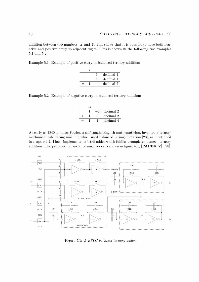
40 CHAPTER 5. TERNARY ARITHMETICS
addition between two numbers, X and Y. This shows that it is possible to have both neg-ative and positive carry to adjacent digits. This is shown in the following two examples5.1 and 5.2.
Example 5.1: Example of positive carry in balanced ternary addition:
1
1 decimal 1+ 1 decimal 1
= 1 −1 decimal 2
Example 5.2: Example of negative carry in balanced ternary addition:
−1
1 −1 decimal 2+ 1 −1 decimal 2
= 1 1 decimal 4
As early as 1840 Thomas Fowler, a self-taught English mathematician, invented a ternarymechanical calculating machine which used balanced ternary notation [23], as mentionedin chapter 4.2. I have implemented a 1 trit adder which fulfills a complete balanced ternaryaddition. The proposed balanced ternary adder is shown in figure 5.1, [PAPER V], [28].
+ CLKC1
C2
C3
C4
C5
C6
C9X
Y
C10
C14
C17
C15
C21
C20
C19
C18
C16
C11
i 3 i 6 i 10
i 9i 7
i 5i 2
i 1
i 8
i 4 C−HIGH
C−LOW
C12
C13
C8
C7
+ CLK
+ CLK
+ CLK + CLK
+ CLK
+ CLK + CLK
+ CLK+ CLK
AZC
AZC
AZC
AZC
+ CLK
+ CLK
+ CLK
+ CLK
− CLK
− CLK
− CLK
− CLK
___
CARRY DETECT
PRE−ADDER
S1
S0
S1
àá âã ä äå æç
èéê êëìíîïðñòóôõ
ö÷øù
ú úû
ü üý
þÿ
! " "# #
$ $% % & &' '
( () ) *+
,-./01
Figure 5.1: A RSFG balanced ternary adder

5.1. INTRODUCTION 41
5.1.2 Balanced Ternary Multiplication
Multiplication in balanced ternary notation is done in the similar manner as with decimalmultiplication. The truth table of a balanced ternary multiplication is shown in table 5.2.Multiplication is done one digit a time. The choice of each digit is simple, if the digit is−1 then invert, if it is 0 then set it to zero, if it is 1 then multiply by one.
Table 5.2: The truth table of a balanced ternary multiplication circuit
−1 0 1
−1 1 0 −1
0 0 0 0
1 −1 0 1
For example the multiplication of (2 ∗ 8 = 16)10 in decimal notation, is (1 − 1)3 ∗ (10− 1)3 = (1− 1− 1 1)3 in balanced ternary notation. The calculation is done as shown inexample 5.3. In the first row the multiplicand is inverted by using ’ternary inversion’. Inthe second row, shift one left, then multiply with ’0’. In the third row, shift left, and thenmultiply with ’1’. Then the three numbers are added together using a balanced ternaryadder.
Example 5.3: An example of a balanced ternary multiplication
−1 1 Invert multiplicand0 0 0 times multiplicand
1 −1 1 times multiplicand
1 −1 −1 1 decimal 16
5.1.3 Balanced Ternary Division
Division in balanced ternary becomes more complex with the possibility of both positiveand negative digits in the quotient. (280)10 divided by 810 = (35)10, becomes (1 0 1 1 01)3 divided by (1 0 -1)3 = (1 1 0 -1)3 in balanced ternary notation. It is calculated asshown in example 5.4.

42 CHAPTER 5. TERNARY ARITHMETICS
Example 5.4: An example of a balanced ternary long division.
1 1 0 −1 quotient (35)
1 0 1 1 0 1 : 1 0 -1 dividend (280) : divisor (8)−1 0 1 subtract by inverting the divisor and add
1 −1 1 0 1 intermediate result−1 0 1 subtract by inverting the divisor and add
−1 0 1 intermediate result, note this is a negative valueintermediate result moved over by two digits,
hence next digit in quotient is zero1 0 −1 subtract by adding divisor
0 remainder eqals zero
5.2 Balanced Ternary Adder Implementation
My contribution in the balanced ternary arithmetic, is the hardware implementationof a Balanced Ternary Adder (BTA) [PAPER V], [28] and balanced ternary counters[PAPER VI, [30]. A BTA is an essential component in arithmetic circuits, and is usedin multiplication and division structures. The first implementation of a one trit adder,which was presented in 2006, [PAPER V], takes two ternary inputs (X and Y ) and gen-erate the SUM output (S0 and S1). The complete schematic diagram of the first BalancedTernary Adder circuit is shown in figure 5.1. The balanced ternary adder is realized usingRSFG structures. The functionality of the circuit is described in detail in [PAPER V].The measurement results are analysed in section 5.4.
5.2.1 Fast Addition Using Balanced Ternary Notation
The balanced ternary (4,2) counter in figure 5.2 [PAPER VI], is comparable with aternary full adder, where the carry signal can have all logic values (−1 , 0 and 1)2. Thebalanced ternary (4,2) counter is a modification of the BTA presented in [PAPER V],and has similar functionalities. A (4,2) ternary counter has 4 balanced ternary inputs(X1...X4) and two balanced ternary outputs (S0, S1). A (4,2) counter is also known as a4 to 2 reducer [72]. A balanced ternary counter sums up the inputs Xi, where i is numberof trits of the same weight, and gives an output in balanced ternary notation. Table 5.3shows the truth table of the (4,2) counter. The functionality is presented in the publishedarticle [PAPER VI].
This thesis presents balanced ternary adder structures using ternary counters. Anexample of a 4 trits balanced ternary adder is shown in figure 5.3. Most of the binaryadder structures are directly inter-exchangeable with balanced ternary adder structures.This means that it is possible to replace the binary full adders with balanced ternarycounters, and still have the same functionality.
Examples are shown in [PAPER VI]. However there are advantages when usingbalanced ternary notation; you do not have to worry about the sign bit, and you need less
2The logic levels are: −1 = 100mV , 0 = 500mV and 1 = 900mV , Vdd = 1V
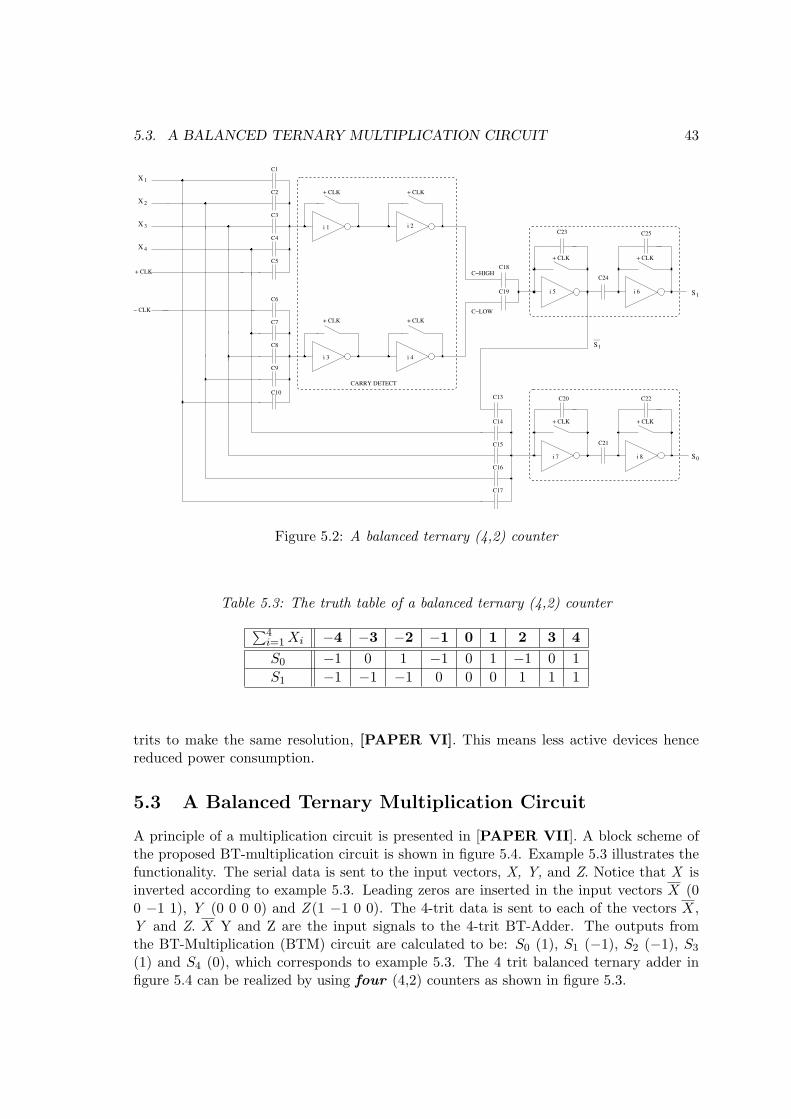
5.3. A BALANCED TERNARY MULTIPLICATION CIRCUIT 43
C1
C2
C3
C24
i 6i 5
C4
C5
C6
C7
C8
C9
C10
C23 C25
C18
C19
C−LOW
C−HIGH
− CLK
+ CLK
i 1
i 3
i 2
i 4
S
C20
C21
C22
i 7 i 8
+ CLK + CLK
+ CLK+ CLK
+ CLK
+ CLK + CLK
+ CLK
0
4
X
X
X
2
1X
3
__
CARRY DETECT
C14
C13
S
C15
C16
C17
S1
2 23
1
4 45
6 67
8 89 9
: :: :
;;
< <= =
> >? ?
@ @A A
BC
DE
FG
HI
JK
LM
NO
PQ
RS TU V VW W
X XY YZ[\]_
` `a a
bc
de
fg
hi
j jk lm
no
pq
r rs s tu
vw x xy
z z
| |
~ ~
Figure 5.2: A balanced ternary (4,2) counter
Table 5.3: The truth table of a balanced ternary (4,2) counter
∑4i=1Xi −4 −3 −2 −1 0 1 2 3 4
S0 −1 0 1 −1 0 1 −1 0 1
S1 −1 −1 −1 0 0 0 1 1 1
trits to make the same resolution, [PAPER VI]. This means less active devices hencereduced power consumption.
5.3 A Balanced Ternary Multiplication Circuit
A principle of a multiplication circuit is presented in [PAPER VII]. A block scheme ofthe proposed BT-multiplication circuit is shown in figure 5.4. Example 5.3 illustrates thefunctionality. The serial data is sent to the input vectors, X, Y, and Z. Notice that X isinverted according to example 5.3. Leading zeros are inserted in the input vectors X (00 −1 1), Y (0 0 0 0) and Z (1 −1 0 0). The 4-trit data is sent to each of the vectors X,Y and Z. X Y and Z are the input signals to the 4-trit BT-Adder. The outputs fromthe BT-Multiplication (BTM) circuit are calculated to be: S0 (1), S1 (−1), S2 (−1), S3
(1) and S4 (0), which corresponds to example 5.3. The 4 trit balanced ternary adder infigure 5.4 can be realized by using four (4,2) counters as shown in figure 5.3.
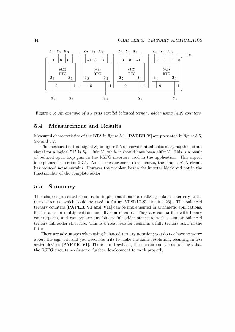
44 CHAPTER 5. TERNARY ARITHMETICS
(4,2)
BTC
(4,2)
BTC
(4,2)
BTC
(4,2)
S 0S 1S 2S 3S 4
S 1 S 0S 2 S 1S 3 S 2S 4 S 3
YZ ZX XY YZ ZX XY0C
0 01 01 12 23 23 3
0 00 00 00 0 10 −11
0
−1
001 0−1 1
BTC
−1
Figure 5.3: An example of a 4 trits parallel balanced ternary adder using (4,2) counters
5.4 Measurement and Results
Measured characteristics of the BTA in figure 5.1, [PAPER V] are presented in figure 5.5,5.6 and 5.7.
The measured output signal S0 in figure 5.5 a) shows limited noise margins; the outputsignal for a logical ”1” is S0 = 96mV , while it should have been 400mV . This is a resultof reduced open loop gain in the RSFG inverters used in the application. This aspectis explained in section 2.7.1. As the measurement result shows, the simple BTA circuithas reduced noise margins. However the problem lies in the inverter block and not in thefunctionality of the complete adder.
5.5 Summary
This chapter presented some useful implementations for realizing balanced ternary arith-metic circuits, which could be used in future VLSI/ULSI circuits [25]. The balancedternary counters [PAPER VI and VII] can be implemented in arithmetic applications,for instance in multiplication- and division circuits. They are compatible with binarycounterparts, and can replace any binary full adder structure with a similar balancedternary full adder structure. This is a great leap for realizing a fully ternary ALU in thefuture.
There are advantages when using balanced ternary notation; you do not have to worryabout the sign bit, and you need less trits to make the same resolution, resulting in lessactive devices [PAPER VI]. There is a drawback, the measurement results shows thatthe RSFG circuits needs some further development to work properly.

5.5. SUMMARY 45
S S S S S
Y
X 0 0 1
1
0 0
0
4 TRITS BALANCED TERNARY ADDER
Z
YZZ Y Y Y X X XXZZ
SERIAL DATA
0
10 −1 −1 1
−1
−1
0 0
0124 3
000 111 222 333
__
Figure 5.4: An example of a balanced ternary multiplication
(a) Output S0 (b) Output S1
Figure 5.5: Measured output characteristics of the BTA circuit, with input signal (−1, −1)
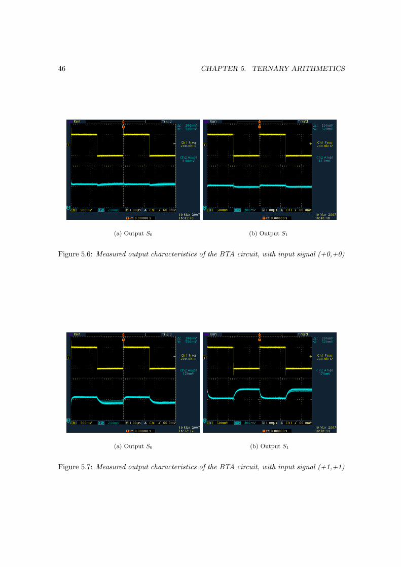
46 CHAPTER 5. TERNARY ARITHMETICS
(a) Output S0 (b) Output S1
Figure 5.6: Measured output characteristics of the BTA circuit, with input signal (+0,+0)
(a) Output S0 (b) Output S1
Figure 5.7: Measured output characteristics of the BTA circuit, with input signal (+1,+1)

Chapter 6
CONCLUSIONS AND FUTUREWORK
This thesis has focused on balanced ternary arithmetic and logic. The main focus isbalanced ternary adders, which can be used in present adder structures. The implemen-tation is realised using recharged semi-floating gate (RSFG) transistors. This is a noveltechnology and needs some more research to achieve a robust workable design.
6.1 Summary
The aim of this work has been to look into balanced ternary applications, which can beused in a future CPU design. At the moment the RSFG technology proposed in this thesisis still far away from commercialisation; however the technology has potential in the designof future ternary VLSI architectures.
6.1.1 Ternary Logic
Ternary inverters, MAX and MIN circuits, down literal circuits and comparison circuits(MLE) are presented and analyzed. The results of the simulations give promising as-pects, which hopefully could lead to fully use of ternary logic instead of binary logic ina CPU in the future. However as the measurement results show; there are still room forimprovement.
6.1.2 Ternary Adder Structures
The balanced ternary counters (3,2) and (4,2) published in this thesis are promising, theycould be used in arithmetic applications, for instance in multiplication and division circuits.They are directly compatible with binary counterparts, and a balanced ternary full addercan replace most off the binary full adder structure. It is also possible to multiply bothnegative and positive numbers using the same architecture, compared with binary logicwhich have to use two’s complement1. This could lead to faster multiplication circuits,
1A two’s-complement system or two’s-complement arithmetic is a system in which negative numbersare represented by the two’s complement of the absolute value
47

48 CHAPTER 6. CONCLUSIONS AND FUTURE WORK
and less complex architectures. You need less trits to make the same resolution, resultingin less active devices therefore reduced power consumption. This is a great leap towardrealizing a fully working ternary ALU in the future.
6.1.3 Hardware
The hardware was implemented using recharge semi-floating transistors, by using a 90nmCMOS process from STMicroelectronics. The capacitors were made by using metal-to-metal stacking (only two metal layers). The architectures presented in this thesis show thepotential of the balanced ternary arithmetic. I have proved it is possible to build hardwareusing balanced ternary logic, and even making simple arithmetic functions. This is a veryearly attempt to build a functional ternary architecture; it is still a long way ahead.Additionally, there will be a need to introduce some redundancy in the circuit design.This is one important topic which needs further investigation, if we want to confirm thatthe design is able to achieve a minimum level of robustness.
At present there does not exist electronic components which in its nature have threestable states. Binary logic uses transistors which can be switched ’on’ or ’off’. This limitsthe development of ternary architectures for the moment.
6.1.4 Results
The fabricated chip is not provided with a ternary output buffer. The measurement isdone with a recharge clock frequency of 200 KHz with an output load of 8pF, 10MΩ.Results from the simulations give satisfactory performance at 1 GHz with a load of 10fF,including parasitic capacitance from the extracted layout of the chip. The circuits in thisthesis are not tested for robustness, and do not have to be seen as fully functional. Theproposed circuits will have to be redesigned to achieve better tolerance, e.g. performingMonte Carlo simulations.
6.2 Future Work
The goal of making a true balanced ternary CPU was my driving force for my investigationto design a better balanced ternary solution. I will try to optimize the RSFG technology,and look into low-voltage applications. Additionally even try sub-threshold logic. I alsoplan to look into some interesting aspects where the supply voltage (Vdd ) is replaced witha sophisticated clocking scheme, to reduce the total power consumption [12].

Chapter 7
PUBLICATIONS
49

50

7.1 PAPER I: Max and Min Functions UsingMultiple-Valued Recharged Semi-Floating Gate
Circuits
Henning Gundersen and Yngvar BergDepartment of informatics, University of Oslo
Proceedings of 2004 IEEE International Symposium on Circuits and Systems,ISCAS, Vancouver Canada, May 23-26, 2004,
ISBN 0-7803-8252-8, Page 857-860
51

52

MAX AND MIN FUNCTIONS USING MULTIPLE-VALUED RECHARGEDSEMI-FLOATING GATE CIRCUITS
H. Gundersen and Y. Berg
Department of Informatics, University of Oslo, Blindern, N-0316 Oslo, [email protected]
ABSTRACT
In this paper we present a new proposal for implementinga voltage-mode Multiple-Valued (MV) maximum or min-imum function. The circuit has been implemented usingRecharged Semi Floating-Gate (SFG) transistors. The ben-efit with this design is, the proposed circuits can easily befabricated using a conventional CMOS process. The cir-cuit is suitable for a low power design, Vdd < 2 volt. It hashigh noise margin and good linearity. The simulation resultsfor the proposed circuit are evaluated using AMS 0.35µmCMOS device parameters.
1. INTRODUCTION
Multiple-valued logic has in the last few decades been pro-posed as a possible alternative to binary logic. Whereas bi-nary logic is limited to only two states, ”true” and ”false”,multiple-valued logic (MVL) replaces these with finitely orinfinitely numbers of values. A MVL system is defined as asystem operating on a higher radix than two [1]. A radix-nset has n elements, 0, 1, ...., n-1. The feasibility of MVLdepends on the availability of the devices constructed forMVL operations [2]. The devices should be able to switchbetween the different logical levels, and preferably be lesscomplex than the binary counterparts.
The multiple-input FG transistors can be used to sim-plify the design of multiple-valued logic [3]. The ini-tial charge on the floating-gates may vary significantly andtherefore impose a very severe inaccuracy unless we applysome form of initialization. Some work on floating-gate re-set strategies have been presented [4] [5].
By recharging of the semi-floating-gate (SFG) we do notonly avoid the problems linked to programming or initial-izing of the floating gates, but we convert the non-volatilefloating gates to semi-floating-gates. The control of the ac-tual floating gate charges in terms of predictable long termcharge restoration becomes easier. The SFG is not influ-enced by a random FG charge distortion due to a periodicor frequent charge restoration or reset. The recharge of theSFGs is accomplished by a local recharge transistor or a
pass gate temporarily connecting the output to the floatinggate of a gate.
One of the most fundamental function in all digital logicis the inverter or the NOT function. The Recharged SFG bi-nary inverter and the SFG MVL inverter will briefly be pre-sented in section 2. Section 3 covers an important functionin Multiple-valued Logic, the Down-Literal Circuit. In sec-tion 4 we look closer on the Pass Gate circuit. Section 5 willlook upon realization of the voltage mode MAX and MINfunctions using SFG Recharged Logic.
2. RECHARGED SFG INVERTERS
2.1. The SFG Recharged Binary Inverter
Clk
Vin
Vsfg
VoutVout
Ne
Pe
VsfgVinCi CiClk
Fig. 1. SFG binary inverter. The transistor sizes are Pe (w =
3.0µm and l = 0.35µm ) and Ne (w = 0.6µm and l = 0.35µm ).The capacitor Ci is equal to 7.7fF
The inverter is truly a fundamental gate in all digi-tal logic. The simple Recharged single input SFG BinaryInverter[5] is shown in Figure 1. The SFG Binary Inverteracts just like an ordinary inverter, except it has a rechargeClk signal, the transfer characteristics is given in Figure 7,output signal labeled Bin Inverter. As we can see theoutput signal is “0” or “1” in the validation period of therecharged signal and Vdd/2 in the recharge period.
2.2. The SFG Recharged MVL Inverter
The analog inverter is very useful for realization of the NOTfunction in multi-valued logic[6]. In order to make a voltage
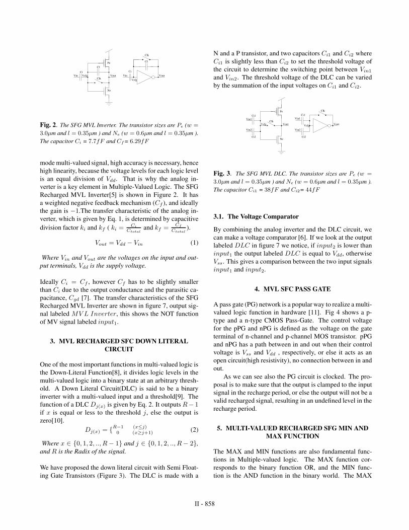
Clk
Clk
Cf
Cf
Vin
Vsfg
VoutVout
Ne
VsfgVinCi
Pe
Ci
Fig. 2. The SFG MVL Inverter. The transistor sizes are Pe (w =
3.0µm and l = 0.35µm ) and Ne (w = 0.6µm and l = 0.35µm ).The capacitor Ci = 7.7fF and Cf= 6.29fF
mode multi-valued signal, high accuracy is necessary, hencehigh linearity, because the voltage levels for each logic levelis an equal division of Vdd. That is why the analog in-verter is a key element in Multiple-Valued Logic. The SFGRecharged MVL Inverter[5] is shown in Figure 2. It hasa weighted negative feedback mechanism (Cf ), and ideallythe gain is −1.The transfer characteristic of the analog in-verter, which is given by Eq. 1, is determined by capacitivedivision factor ki and kf ( ki =
Ci
Ctotaland kf =
Cf
Ctotal).
Vout = Vdd − Vin (1)
Where Vin and Vout are the voltages on the input and out-put terminals, Vdd is the supply voltage.
Ideally Ci = Cf , however Cf has to be slightly smallerthan Ci due to the output conductance and the parasitic ca-pacitance, Cgd [7]. The transfer characteristics of the SFGRecharged MVL Inverter are shown in figure 7, output sig-nal labeled MV L Inverter, this shows the NOT functionof MV signal labeled input1.
3. MVL RECHARGED SFC DOWN LITERALCIRCUIT
One of the most important functions in multi-valued logic isthe Down-Literal Function[8], it divides logic levels in themulti-valued logic into a binary state at an arbitrary thresh-old. A Down Literal Circuit(DLC) is said to be a binaryinverter with a multi-valued input and a threshold[9]. Thefunction of a DLC Dj(x) is given by Eq. 2. It outputs R− 1
if x is equal or less to the threshold j, else the output iszero[10].
Dj(x) = R−1 (x≤j)
0 (x≥j+1) (2)
Where x ∈ 0, 1, 2, .., R − 1 and j ∈ 0, 1, 2, .., R − 2,and R is the Radix of the signal.
We have proposed the down literal circuit with Semi Float-ing Gate Transistors (Figure 3). The DLC is made with a
N and a P transistor, and two capacitors Ci1 and Ci2 whereCi1 is slightly less than Ci2 to set the threshold voltage ofthe circuit to determine the switching point between Vin1
and Vin2. The threshold voltage of the DLC can be variedby the summation of the input voltages on Ci1 and Ci2.
Clk
Vsfg
Vin2
Vin1
Ci2
Ci1
Vout
Vin1
Vin2
Ci1
Vsfg
Ci2
ClkVout
Ne
Pe
!"# $ $%&'( ()
*+, ,-
./01
Fig. 3. The SFG MVL DLC. The transistor sizes are Pe (w =
3.0µm and l = 0.35µm ) and Ne (w = 0.6µm and l = 0.35µm ).The capacitor Ci1 = 38fF and Ci2= 44fF
3.1. The Voltage Comparator
By combining the analog inverter and the DLC circuit, wecan make a voltage comparator [6]. If we look at the outputlabeled DLC in figure 7 we notice, if input2 is lower thaninput1 the output labeled DLC is equal to Vdd, otherwiseVss. This gives a comparison between the two input signalsinput1 and input2.
4. MVL SFC PASS GATE
A pass gate (PG) network is a popular way to realize a multi-valued logic function in hardware [11]. Fig 4 shows a p-type and a n-type CMOS Pass-Gate. The control voltagefor the pPG and nPG is defined as the voltage on the gateterminal of n-channel and p-channel MOS transistor. pPGand nPG has a path between in and out when their controlvoltage is Vss and Vdd , respectively, or else it acts as anopen circuit(high resistivity), no connection between in andout.
As we can see also the PG circuit is clocked. The pro-posal is to make sure that the output is clamped to the inputsignal in the recharge period, or else the output will not be avalid recharged signal, resulting in an undefined level in therecharge period.
5. MULTI-VALUED RECHARGED SFG MIN ANDMAX FUNCTION
The MAX and MIN functions are also fundamental func-tions in Multiple-valued logic. The MAX function cor-responds to the binary function OR, and the MIN func-tion is the AND function in the binary world. The MAX

Ne
In Out In Out
Pe
pPGClk
(a) pPG
Ne
Pe
In Out OutIn nPGClk
(b) nPG
Fig. 4. The Pass Gate Circuits. The transistor sizes are Pe (w =
0.6µm and l = 0.35µm ) and Ne (w = 0.6µm and l = 0.35µm ).
and MIN function has been presented earlier using Neuron-MOS Transistors[6], [10],[12]. However another way ofrealizing these functions is by using Semi-Floating GateRecharge Logic. This makes it possible to implement a low-power digital system with reduced dynamic power dissipa-tion. The advantage of this technology is presented in [5]and the circuit is presented in fig 5. As we can see the cir-cuit use the analog inverter and the DLC to make a voltagecomparator. It then gives a selection signals to the Pass-Gate network, which consists of a pPass-Gate and a nPass-Gate circuit, If the output signal labeled DLC is “high”,input1 is selected, and if the signal labeled DLC is “low”,input2 is selected. Just by changing the pPass-Gate(nPG)with a nPass-Gate(nPG) and nPG with pPG we can achievethe minimum function as shown in fig 6. The output of theMIN circuit (labeled Minimum) is shown in fig 7.
The heart of this circuit is the analog inverter and theDLC. We know that the analog inverter can be made withhigh linearity and good precision, just by adjustment of C1
and C2. This is described in [7]. As mentioned in section 3the DLC divides logic levels in the multi-valued logic into abinary state at an arbitrary threshold. The DLC is a 2 inputinverter, and by making C4 slightly less than C3, we makesure the threshold voltage is set correct, and the output of theDLC is set “high” when Input1 is equal to Input2, hencePassGate network will work properly.
OutputDLC OutC4
C5
MVL Inv
Out
nPG
pPGInput 2
Input 1
C1
C2 C3
Bin-
Out
Clk ClkClk
!" "#
$%
&'
( ()
* *+
, ,-. ./012 23
4 456 67
Fig. 5. The MVL Recharged SFG Max Circuit. The capacitors C1
= 7.7fF , C2= 6.3fF , C3 = 38fF , C4= 44fF and C5 = 7.7fF
OutputDLC OutC4
MVL Inv
Out
nPG
pPG
Bin-
Out
Input 1
Input 2
C1
C2 C3
C5
ClkClkClk
8 89 : :;< <=
> >?@ @AB BC
D DE
FG
H HIJ JKLM
N NO
P PQ
R RS
TU
VWXYZ[\ \]
^ ^_
Fig. 6. The MVL Recharged SFG Min Circuit. The capacitors C1
= 7.7fF , C2= 6.3fF , C3 = 38fF , C4= 44fF and C5 = 7.7fF
0 0.2 0.4 0.6 0.8 1 1.2 1.4 1.6 1.8 2 2.2 2.4 2.6 2.8 3 3.2
x 106
00.5
11.5
2
Clo
ck
0 0.2 0.4 0.6 0.8 1 1.2 1.4 1.6 1.8 2 2.2 2.4 2.6 2.8 3 3.2
x 106
00.5
11.5
2
MV
L I
nve
rte
r
0 0.2 0.4 0.6 0.8 1 1.2 1.4 1.6 1.8 2 2.2 2.4 2.6 2.8 3 3.2
x 106
00.5
11.5
2D
LC
0 0.2 0.4 0.6 0.8 1 1.2 1.4 1.6 1.8 2 2.2 2.4 2.6 2.8 3 3.2
x 106
00.5
11.5
2
Bin
In
ve
rte
r
0 0.2 0.4 0.6 0.8 1 1.2 1.4 1.6 1.8 2 2.2 2.4 2.6 2.8 3 3.2
x 106
00.5
11.5
2
Inp
ut
1
0 0.2 0.4 0.6 0.8 1 1.2 1.4 1.6 1.8 2 2.2 2.4 2.6 2.8 3 3.2
x 106
00.5
11.5
2
Inp
ut
2
0 0.2 0.4 0.6 0.8 1 1.2 1.4 1.6 1.8 2 2.2 2.4 2.6 2.8 3 3.2
x 106
00.5
11.5
2
Ma
xim
um
0 0.2 0.4 0.6 0.8 1 1.2 1.4 1.6 1.8 2 2.2 2.4 2.6 2.8 3 3.2
x 106
00.5
11.5
2
Time (s)
Min
imu
m
Fig. 7. The Maximum and Minimum Plot (radix 16), simulatedwith Cadence 4.4.5.100.10 with spectre simulation tool using AMS0.35µm CMOS device parameters Hit Kit version: 3.30.42.00.
"Max"
"Max"
"Max" Out 1
Out 2
Input 2
Input 4
Input 3MAX Out
Input 1
Fig. 8. The 4 input MAX Circuit
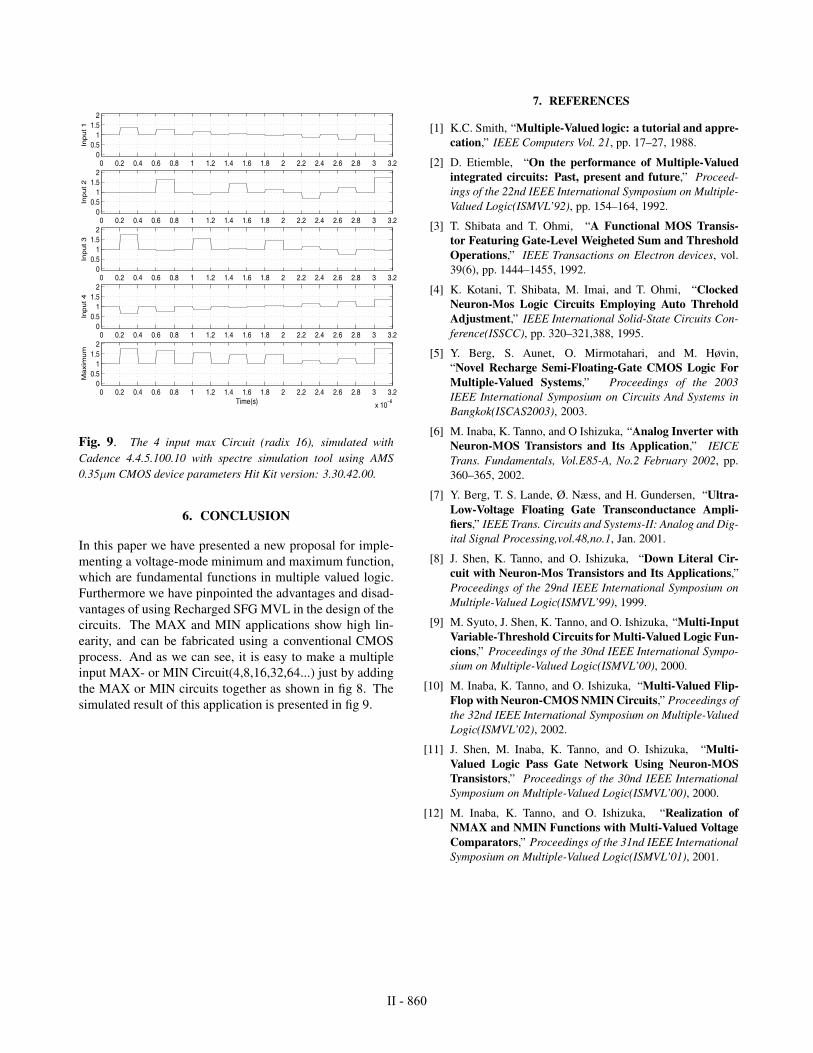
0 0.2 0.4 0.6 0.8 1 1.2 1.4 1.6 1.8 2 2.2 2.4 2.6 2.8 3 3.2
x 106
00.5
11.5
2
Inp
ut
1
0 0.2 0.4 0.6 0.8 1 1.2 1.4 1.6 1.8 2 2.2 2.4 2.6 2.8 3 3.2
x 106
00.5
11.5
2
Inp
ut
2
0 0.2 0.4 0.6 0.8 1 1.2 1.4 1.6 1.8 2 2.2 2.4 2.6 2.8 3 3.2
x 106
00.5
11.5
2
Inp
ut
3
0 0.2 0.4 0.6 0.8 1 1.2 1.4 1.6 1.8 2 2.2 2.4 2.6 2.8 3 3.2
x 106
00.5
11.5
2
Inp
ut
4
0 0.2 0.4 0.6 0.8 1 1.2 1.4 1.6 1.8 2 2.2 2.4 2.6 2.8 3 3.2
x 106
00.5
11.5
2
Time(s)
Ma
xim
um
Fig. 9. The 4 input max Circuit (radix 16), simulated withCadence 4.4.5.100.10 with spectre simulation tool using AMS0.35µm CMOS device parameters Hit Kit version: 3.30.42.00.
6. CONCLUSION
In this paper we have presented a new proposal for imple-menting a voltage-mode minimum and maximum function,which are fundamental functions in multiple valued logic.Furthermore we have pinpointed the advantages and disad-vantages of using Recharged SFG MVL in the design of thecircuits. The MAX and MIN applications show high lin-earity, and can be fabricated using a conventional CMOSprocess. And as we can see, it is easy to make a multipleinput MAX- or MIN Circuit(4,8,16,32,64...) just by addingthe MAX or MIN circuits together as shown in fig 8. Thesimulated result of this application is presented in fig 9.
7. REFERENCES
[1] K.C. Smith, “Multiple-Valued logic: a tutorial and appre-cation,” IEEE Computers Vol. 21, pp. 17–27, 1988.
[2] D. Etiemble, “On the performance of Multiple-Valuedintegrated circuits: Past, present and future,” Proceed-ings of the 22nd IEEE International Symposium on Multiple-Valued Logic(ISMVL’92), pp. 154–164, 1992.
[3] T. Shibata and T. Ohmi, “A Functional MOS Transis-tor Featuring Gate-Level Weigheted Sum and ThresholdOperations,” IEEE Transactions on Electron devices, vol.39(6), pp. 1444–1455, 1992.
[4] K. Kotani, T. Shibata, M. Imai, and T. Ohmi, “ClockedNeuron-Mos Logic Circuits Employing Auto ThreholdAdjustment,” IEEE International Solid-State Circuits Con-ference(ISSCC), pp. 320–321,388, 1995.
[5] Y. Berg, S. Aunet, O. Mirmotahari, and M. Høvin,“Novel Recharge Semi-Floating-Gate CMOS Logic ForMultiple-Valued Systems,” Proceedings of the 2003IEEE International Symposium on Circuits And Systems inBangkok(ISCAS2003), 2003.
[6] M. Inaba, K. Tanno, and O Ishizuka, “Analog Inverter withNeuron-MOS Transistors and Its Application,” IEICETrans. Fundamentals, Vol.E85-A, No.2 February 2002, pp.360–365, 2002.
[7] Y. Berg, T. S. Lande, Ø. Næss, and H. Gundersen, “Ultra-Low-Voltage Floating Gate Transconductance Ampli-fiers,” IEEE Trans. Circuits and Systems-II: Analog and Dig-ital Signal Processing,vol.48,no.1, Jan. 2001.
[8] J. Shen, K. Tanno, and O. Ishizuka, “Down Literal Cir-cuit with Neuron-Mos Transistors and Its Applications,”Proceedings of the 29nd IEEE International Symposium onMultiple-Valued Logic(ISMVL’99), 1999.
[9] M. Syuto, J. Shen, K. Tanno, and O. Ishizuka, “Multi-InputVariable-Threshold Circuits for Multi-Valued Logic Fun-cions,” Proceedings of the 30nd IEEE International Sympo-sium on Multiple-Valued Logic(ISMVL’00), 2000.
[10] M. Inaba, K. Tanno, and O. Ishizuka, “Multi-Valued Flip-Flop with Neuron-CMOS NMIN Circuits,” Proceedings ofthe 32nd IEEE International Symposium on Multiple-ValuedLogic(ISMVL’02), 2002.
[11] J. Shen, M. Inaba, K. Tanno, and O. Ishizuka, “Multi-Valued Logic Pass Gate Network Using Neuron-MOSTransistors,” Proceedings of the 30nd IEEE InternationalSymposium on Multiple-Valued Logic(ISMVL’00), 2000.
[12] M. Inaba, K. Tanno, and O. Ishizuka, “Realization ofNMAX and NMIN Functions with Multi-Valued VoltageComparators,” Proceedings of the 31nd IEEE InternationalSymposium on Multiple-Valued Logic(ISMVL’01), 2001.

7.2 PAPER II: A Novel Ternary Switching Element UsingCMOS Recharged Semi-Floating Gate Devices
Henning Gundersen, Rene Jensen and Yngvar BergDepartment of informatics, University of Oslo
Proceedings of 35th International Symposium on Multiple-Valued Logic,ISMVL, Calgary Canada, May 19-21, 2005,
ISBN 0-7695-2336-6, Page 54-58
57

58

A Novel Ternary Switching Element Using CMOS Recharge Semi
Floating-Gate Devices
Henning Gundersen, Rene Jensen and Yngvar Berg
University of Oslo, Department of Informatics,
P.O.Box 1080, Blindern, NO-0316 Oslo, Norway. Fax: +47 22 85 24 01.
E-mail: [email protected]
Abstract
In this paper we present a novel voltage mode non-inverting CMOS Semi Floating-Gate(SFG) TernarySwitching Element. The design is applicable for re-constructing or refreshing ternary logic signals. Theswitching points are tuned using capacitive division.A preliminary simulation results from Cadence Spectrewith AMS 0.35µmprocess parameters c35b4 is included.
1 Introduction
Multiple-valued logic has in the last few decadesbeen proposed as a possible alternative to binary logic.Whereas binary logic is limited to only two states,”true” and ”false”, multiple-valued logic (MVL)replaces these with finitely or infinitely numbers ofvalues.
The history of Multi-valued Logic as a separate ob-ject began in the early 1920 by a polish philosopherLukasiewicz [1]. His intention was to introduce a thirdadditional truth-value for ”possible”. The outcome ofthis investigation is known as the Lukasiewicz systems.Parallel to the approach of Lukasiewicz, the Americanmathematician Emil Post [2], introduced the idea ofan additional truth degrees, and used this approach tosolve the problems of the represent ability of functions,also known as the Post Algebra.
1.1 Ternary logic
Ternary logic has three logic states, ”0”,”1” and”2”, and the optimum radix of a fractional number isfound to be the natural logarithm (e). Ternary logicuses number representation with radix=3, compared
to binary logic witch uses radix=2, hence the mosteconomical integer radix which is the closest to thenatural logarithm e, is the number 3 [3]. This specialproperty of base 3, inspired the early computerdesigners to build a ternary computer.
The first approach to build a MV-computer withternary architecture was in the early 50th. in the USA.The earliest published discussion appears in the 1950book High-Speed Computing Devices, a survey of com-puter technologies compiler on the behalf of the U.SNavy, by the staff of Engineering Research Associates[4]. But the first working ternary computer was builtin Russia at the Moscow State University in 1958. Thecomputer was design by Nikolai P. Brusentow and hiscolleagues and they named it Setun, for a river thatflows near the university campus [5]. From 1958 to1965 some 50 machines where built.
1.2 Floating Gate (FG) Transistors
The multiple-input FG transistors can be used tosimplify the design of multiple-valued logic [6]. Theinitial charge on the floating-gates may vary signifi-cantly and therefore impose a very severe inaccuracyunless we apply some form of initialization. Some workon floating-gate reset strategies have been presented byKotami et.al. [7], and by Berg et.al. [8].
1.3 Recharge Semi-Floating Gate (RSFG) Logic
As mentioned earlier FG circuits need to be initial-ized, either once initially or frequently. The once andfor all initialization is synonymous with programming.By recharging the SFG frequently we avoid problemswith any leakage currents and random or undesireddisturbance of the floating-gate charges. The resetor recharge scheme can be used to overcome someproblems associated with floating-gate circuit design
Proceedings of the 35th International Symposium on Multiple-Valued Logic (ISMVL’05) 0195-623X/05 $ 20.00 IEEE

Vin VinVout Vout
Clk
Clk
V V
Pe
Ne
sfg sfg
Ci Ci
Figure 1. A SFG recharge binary inverter. TheClk pulse is given by the recharge frequency whichis twice the frequency of the input signal.
[8]. The recharge condition is different than the resetin clocked-Neuron-MOS logic proposed by Kotamiet.al. [7].
When reseting or recharging a gate the inputs arerecharged simultaneously and not set to a referencevoltage, normally Vss or Vdd. While recharging thegates are short-circuited and the output and thesemi-floating-gate of a logic gate is forced to Vdd/2 .
The recharge scheme is similar to biasing ofsingle-ended auto-zeroing comparators which havebeen used in high-speed flash AD converters. Themain purpose of the recharge scheme is to initializeor recharge the semi-floating-gates to an equilibriumstate which can be utilized to yield fast binary andmultiple-valued signal processing. In addition we mayreduce the effect of mismatches, especially transistormismatches, and power supply noise. The rechargescheme provides a simple, fast and accurate rechargeto the equilibrium state for all gates regardless oflogical depth. We use the term Recharge Logic (RL)or Recharge Semi-Floating- Gate Logic (RSFGL) forthe circuits presented in this paper [9]. The SFGcircuits are recharged to the initial equilibrium state.namely Vdd/2 .
A simple binary single input gate, namely an in-verter is shown in figure 1. By equalizing the βs weobtain an equilibrium state when the recharge signalis 1. The output and gate are driven towards Vdd/2.When the recharge signal is 1 we have to distinct cases.Assume that the input signal is initially 1 (Vdd ), theSFG voltage can he expressed as (Vdd/2 ) x ( 1 + ki),where ki = Ci/Ct and Ct is the total capacitance seenby the SFG, and the output is equal to 0. The out-put and the SFG will be forced towards Vdd/2 simul-
taneously. The recharge current which will pull theSFG down towards Vdd/2 , is larger than the equilib-rium current (Ibec). We define the recharge rise rimetr as the time required to recharge the output from 0to Vdd/2 (and the SFG simultaneously). If the inputsignal is initially 0 the SFG voltage is (Vdd/2 ) x (1- ki) and the output is 1 . The recharge current willbe reduced compared to the former case due to bodyeffect of the n-channel recharge transistor. In order toachieve a correct recharge to the equilibrium state ina chain of gates we need to recharge all gates, henceall inputs simultaneously, In addition we need to de-velop a synchronization scheme for the recharge. Wedefine the recharge fall rime tf , as the time requiredto recharge the output from 1 to Vdd/2 . The rechargefrequency is twice the frequency of the input signal.
2 The Recharge Semi Floating-Gate(RSFG) Ternary Switching Element
VoutVin
DLC
DLC
AZC
AZC
AZC
MVL Inverter
Clk
Clk
Clk
2C
C
2C
C
C
C
Cf
Clk
Clk
Clk
Clk
Clk
Clk
___
___
___
Figure 2. Schematic diagram for ternary element.The design comprise three Semi Floating-GateAutoZero blocks (AZC), two SFG Down LiteralCircuits (DLC) and one analog MVL SFG in-verter at the output.
The schematic diagram in figure 2 shows a novelvoltage mode ternary switching element. The designuses three AutoZero circuits, two Semi-Floating Gate(SFG) threshold elements also called a MVL SFGDown Literal Circuit, and a MVL SFG inverter [10].This application is suitable to refresh or reconstructternary voltage mode signals.
Figure 3 shows the output signal of the circuitversus the input signal. The dotted line is the input
Proceedings of the 35th International Symposium on Multiple-Valued Logic (ISMVL’05) 0195-623X/05 $ 20.00 IEEE

0 0.2 0.4 0.6 0.8 1 1.2 1.4 1.6
x 106
0
0.2
0.4
0.6
0.8
1
1.2
1.4
1.6
1.8
2
Time (s)
Vo
lta
ge
(V
)
VinVout
Figure 3. Simulation over 16 clock periods show-ing output versus input voltage.
signal. As we notice the output signal is convergingto three logic levels, 0.2 Volt, 1 Volt and 1.8 Volt.It is also a valid MVL recharge signal. As we no-tice, in the recharge periods, the output is set to Vdd/2 .
2.1 The SFG AutoZero Circuit (AZC)
An AutoZero circuit can been seen as a signal con-verter which either convert a binary , static (Vdd, Vss)or MVL signal to a valid recharge signal. A SFGRecharge AutoZero circuit is shown in figure 2. It setsthe input signal to Vdd/2 in the recharge periods andin the precharge periods the input signal is connectedto the output thru the pass gate transistors. Whilerecharging the output is driven to recharge state de-fined by V out = Vdd/2. Note that the recharge fre-quency is twice the frequency of the input signal.
2.2 The SFG Down Literal Circuit (DLC)
The threshold or the switching point is set by theMVL Recharge SFG DLC circuit [10] as shown in fig-ure 4. A DLC can be seen as a digital inverter withtwo inputs. The dotted line in the figure is the inputsignal. The lower threshold or switching point is set bythe output of the AutoZero Circuit(AZC) connectedto the Vss (Gnd), and the upper switching point is setby the AZC connected to Vdd. The figure shows theinternal switching nodes on the output of the DLC cir-cuit. The switch point is determined by the capacitivedivision factor. ki
1, Vin has weight 2C and VThreshold
1ki = Ci/P
CIn
0.2 0.4 0.6 0.8 1 1.2 1.4 1.6 1.8 20
0.2
0.4
0.6
0.8
1
1.2
1.4
1.6
1.8
2
Vin (s)
Vol
tage
(V
)
Threshold 1Threshold 2
Figure 4. Shows the thresholds for internalswitching elements used for building the ternaryelement. The thresholds or switching points aredetermined by the capacitive division factors as-sociated with each of the two switching elements.
from the AutoZero Circuit, has weight C (C=7.5fF ).By changing this factor we can fine tune the three logiclevels.
2.3 The MVL SFG Inverter
The circuit shown at the output of figure 2, is calleda MVL recharge SFG Inverter [10]. As we notice it hastwo inputs with the same weight (C). The MVL SFGInverter will convert the output signal to a valid MVLrecharge signal. The transfer characteristic of a MVLinverter is given by:
Vout = Vdd − Vin (1)
Where Vin and Vout are the voltages on the input andoutput terminals, Vdd is the supply voltage.
The gain of MVL SFG inverter is determined by the ca-pacitive division factor ki. The feedback capacitor Cf
should be∑
Cin, hence 2C to make sure EQ 1 is true,however Cf has to be slightly smaller than 2C due tothe output conductance and the parasitic capacitance,Cgd.
2.4 The SFG Ternary Switching Element
If we analyze the complete circuit in figure 2, wefind three stable regions given by dVout/dVin, this isshown in figure 5. These three regions are logic level’0’ (0 − 0.35V ), ’1’ (0.8 − 1.2V ) and ’2’ (1.65 − 2.0V ).
Proceedings of the 35th International Symposium on Multiple-Valued Logic (ISMVL’05) 0195-623X/05 $ 20.00 IEEE

0 0.2 0.4 0.6 0.8 1 1.2 1.4 1.6 1.8 2−0.005
0
0.005
0.01
0.015
0.02
0.025
0.03
0.035
Vin (V)
diff(
Vou
t) (
V)
Figure 5. A sweep of the derivative of the outputsignal Vout. Illustrates three stable regions aroundthe three voltage levels 0.2V, 1V and 1.8V.
This gives us, if the input is between 0 − 0.35V it willconverge to logic level ’0’, if the input is 0.8 − 1.2Vthe output will be set to logic level ’1’ and if the inputis in the region 1.65 − 2.0V the output will be set tologic level ’2’. This is also shown in the figure 6 we cansee how the output converge to the three logic levels.
0 0.2 0.4 0.6 0.8 1 1.2 1.4 1.6 1.8 20
0.2
0.4
0.6
0.8
1
1.2
1.4
1.6
1.8
2
Vin (V)
Vou
t (V
)
VinVout
Figure 6. A sweep of the output signal Vout versusthe input signal Vin. This illustrates how valid in-put voltage are moved towards the output voltages0.2, 1, 1.8V.
A graphical illustrations of the noise margins arecalculated in figure 7. The calculations of the noisemargins of the simulated values given by the CadenceSpectre simulation, are obtained by using Matlab.
This calculation confirms the noise margins of theternary circuit. We can see three logic levels ’0’, ’1’and ’2’ respectively 0.2V , 1V and 1.8V .
The switching region or noise is indicated usinggray color, this is where the logic levels are undefined.As we can see we got better noise margins for thelogic level ’1’, but this can be tuned by changing thevalue of the capacitors on the input of the DLC circuit.
0 0.2 0.4 0.6 0.8 1 1.2 1.4 1.6 1.8 20
0.2
0.4
0.6
0.8
1
1.2
1.4
1.6
1.8
2
Vin (s)
Mar
gins
(V
)
Input margins Output margins
’0’
’1’
’2’
Figure 7. Matlab calculations demonstrating thenoise-margin diagram of the ternary element.The analysis is based on circuit simulations inCadence Spectre. The three logical output values0, 1, 2 is found as output voltages 0.2, 1, 1.8Vrespectively. The noise or switching region is in-dicated using gray color.
Figure 8 shows the zero crossing point of the threelogic levels, here is Vin −Vout calculated using Matlab.The zero crossing point, which gives the three logiclevels, is 0.18V , 1.03V and 1.85V this is possible tofine tune by changing the capacitive division factor ki
in the DLC circuit.
3 Conclusions
In this paper we have presented a novel non-inverting voltage mode CMOS Ternary Switching El-ement. This element have shown good noise margins,and it is easy to fine tune, and it is well suitable touse of refreshing ternary signals in memory applica-tions and also to reconstruct internal ternary logic sig-nals. All simulation results are obtained from CadenceSpectre AMS 0.35 µmCMOS device parameters with10MHz precharge clock frequency and 2V power sup-ply. This application can easily be fabricated using aconventional CMOS process.
Proceedings of the 35th International Symposium on Multiple-Valued Logic (ISMVL’05) 0195-623X/05 $ 20.00 IEEE

0 0.2 0.4 0.6 0.8 1 1.2 1.4 1.6 1.8 2−0.25
−0.2
−0.15
−0.1
−0.05
0
0.05
0.1
0.15
0.2
0.25
Vin (s)
Del
ta (
V)
Figure 8. The delta difference between output andinput voltage (Vout − Vin). The results were ob-tained from simulation of the schematic in Ca-dence Spectre using 10MHz precharge clock.
References
[1] Kotarbinsky, “Jan lukasiewicz’s works on the historyof logic,” Studia Logica 8, pp. 57–62, 1958.
[2] M. Davis and Emil L. Post, “His life and work, in mdavis (ed.), solvability, provability, definability : thecollected works of emil l post,” Boston, MA, pp. xi–xxviii, 1994.
[3] Brian Hayes, “Third base,” American Scientist, Vol-ume 89, Number 6, pp. 490–494, Nov-Dec 2001.
[4] Engineneering Research Associates Inc., High-SpeedComputing Devices, McGraw-Hill Book Company Inc.,1950.
[5] N.P.Brusentov, “The computer ’setun’ of moscow uni-versity,” Material of the Scientific-technical Confer-ence: New Developments in Computational Mathe-matics and Computing Techniques, Kiev, pp. 226–234,1960.
[6] T. Shibata and T. Ohmi, “A functional mos transis-tor featuring gate-level weigheted sum and thresholdoperations,” IEEE Transactions on Electron devices,vol. 39(6), pp. 1444–1455, 1992.
[7] K. Kotani, T. Shibata, M. Imai, and T. Ohmi,“Clocked neuron-mos logic circuits employing autothrehold adjustment,” IEEE International Solid-StateCircuits Conference(ISSCC), pp. 320–321,388, 1995.
[8] Y. Berg, S. Aunet, O. Mirmotahari, and M. Høvin,“Novel recharge semi-floating-gate cmos logic formultiple-valued systems,” Proceedings of the 2003IEEE International Symposium on Circuits And Sys-tems in Bangkok(ISCAS2003), 2003.
[9] Y. Berg, S. Aunet, Ø. Næss, O. Mirmotahari, andM. Høvin, “Binary to multiple-valued recharge con-verter for multiple-valued cmos logic,” ECCTD’03-Euopean Conference on Circuit Theory and De-sign,Cracow, Poland, pp. 349–352, 2003.
[10] H. Gundersen and Y. Berg, “Max and min functionsusing multiple-valued recharge semi-floating gate cir-cuits,” Proceedings of the 2004 IEEE InternationalSymposium on Circuits And Systems in Vancouver(ISCAS2004), 2004.
Proceedings of the 35th International Symposium on Multiple-Valued Logic (ISMVL’05) 0195-623X/05 $ 20.00 IEEE


7.3 PAPER III: A Novel Ternary More, Less and EqualityCircuit Using Recharged Semi-Floating Gate Devices
Henning Gundersen and Yngvar BergDepartment of informatics, University of Oslo
Proceedings of 2006 IEEE International Symposium on Circuits and Systems,ISCAS, Kos Greece, May 21-24, 2006,ISBN 0-7803-9390-2, Page 3169-3172
65

66
A Novel Ternary More, Less and Equality CircuitUsing Recharged Semi-Floating Gate Devices
Henning Gundersen and Yngvar BergDepartment of Informatics, Microelectronic Systems Group, University of Oslo
Blindern, NO-0316, Oslo, NorwayEmail: [email protected]
Abstract— This paper presents a novel Ternary More, Lessand Equality (MLE) Circuit implemented with Recharged Semi-Floating Gate Transistors. The circuit is a ternary application,and ternary structures may offer the fastest search in a treestructure. The circuit has two ternary inputs, and one ternaryoutput which will be a comparison of the two ternary inputs.The circuit is a useful building block for use in a search treeapplication. The circuit is simulated by using Cadence R©AnalogDesign Environment with CMOS090 GP process parametersfrom STMicroelectronics, a 90 nm General Purpose Bulk CMOSProcess with 7 metal layers. The circuit operates at a 1 GHz clockfrequency. The supply voltage is +/- 0.5 Volt. All capacitors aremetal plate capacitors, based on a vertical coupling capacitancebetween stacked metal plates.
I. INTRODUCTION
Ternary numbering system gives theoretically the fastestsearch path in a tree structure. An example of a ternarystructure is a telephone menu system, with eight choices. Ifyou are using a binary structure, you will have two choicesfor each level. This gives us the performance number of 4.51.A ternary structure, with three choices for each level, willhave a performance number of 3.75. Which is the optimalnumber. [1].
If you want to test for equality less or more to sort twoinputs, in a binary search tree, you have to use two instructions.In a ternary search tree, you only need one instruction to sorttwo inputs. This paper presents a ternary application whichuses this feature. The truth table of the presented circuit isshown in table I. As shown we use balanced ternary notation,’perhaps the prettiest number system of all’ as Donald Knuthsaid in his book, The Art of Computer Programming [2].The Ternary More, Less and Equality (MLE) Circuit has twoinputs, the left most row (A) and the upper row (B). If A = Bthe output is 0, if A < B the output is 1 and if A > B theoutput is −1.
II. FUNDAMENTAL BUILDING BLOCKS USED IN
RECHARGE SEMI-FLOATING GATE (RSFG) DESIGN
This paper will not cover the fundamental theory of RSFGdevices [3]. It is only the building blocks used in the ternaryMLE circuit that will be focused in this paper.
1The performance number gives the average choices you have to go throughto find the right choice.
TABLE I
THE TRUTH TABLE OF THE TERNARY MORE, LESS AND EQUALITY (MLE)
CIRCUIT
-1 0 1
-1 0 1 1
0 -1 0 1
1 -1 -1 0
A. Floating Gate Transistors
The multiple-input FG transistors can be used to simplifythe design of multiple-valued logic [4]. The initial charge onthe floating-gates may vary significantly and therefore imposea very severe inaccuracy, unless we do apply some form ofinitialization. Some work on floating-gate reset strategies havebeen presented by Kotani et.al. [5], and by Berg et.al. [3].
B. Recharge Semi-Floating Devices
As mentioned, FG circuits need to be initialized, eitheronce initially or frequently. The once and for all initializationis synonymous with programming. By recharging the SFGfrequently we avoid problems with any leakage currents andrandom or undesired disturbance of the floating-gate charges.The reset or recharged scheme can be used to overcome someproblems associated with the floating-gate circuit design[3]. The recharged condition is different than the reset inclocked-Neuron-MOS logic proposed by Kotani et.al. [5].
When reseting or recharging a gate, the inputs arerecharged simultaneously and they are set to a referencevoltage, normally Vdd/2. While recharging, the gates areshort-circuited and the output and the semi-floating-gate of alogic gate is forced to Vdd/2.
The recharged scheme is similar to biasing of single-endedauto-zeroing comparators, which have been used in high-speed flash AD converters. The main purpose of the rechargedscheme is to initialize or recharge the semi-floating-gates to anequilibrium state, which can be utilized to yield fast binary andmultiple-valued signal processing. In addition we may reduce
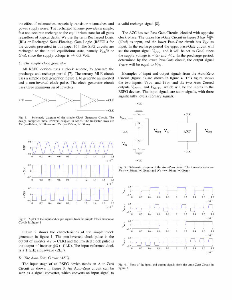
the effect of mismatches, especially transistor mismatches, andpower supply noise. The recharged scheme provides a simple,fast and accurate recharge to the equilibrium state for all gatesregardless of logical depth. We use the term Recharged Logic(RL) or Recharged Semi-Floating- Gate Logic (RSFGL) forthe circuits presented in this paper [6]. The SFG circuits arerecharged to the initial equilibrium state, namely Vdd/2 orGnd, since the supply voltage is +/- 0.5 Volt.
C. The simple clock generator
All RSFG devices uses a clock scheme, to generate theprecharge and recharge period [7]. The ternary MLE circuituses a simple clock generator, figure 1, to generate an invertedand a non-inverted clock pulse. The clock generator circuituses three minimum sized inverters.
REF − CLK
+ CLK
Fig. 1. Schematic diagram of the simple Clock Generator Circuit. Thedesign comprises three inverters coupled in series. The transistor sizes arePe (w=460nm, l=100nm) and Ne (w=120nm, l=100nm)
0 0.2 0.4 0.6 0.8 1 1.2 1.4 1.6 1.8
x 10−8
−0.5
0
0.5
RE
F
0 0.2 0.4 0.6 0.8 1 1.2 1.4 1.6 1.8
x 10−8
−0.5
0
0.5
− C
LK
0 0.2 0.4 0.6 0.8 1 1.2 1.4 1.6 1.8
x 10−8
−0.5
0
0.5
+ C
LK
Fig. 2. A plot of the input and output signals from the simple Clock GeneratorCircuit in figure 1
Figure 2 shows the characteristics of the simple clockgenerator in figure 1. The non-inverted clock pulse is theoutput of inverter #2 (+ CLK) and the inverted clock pulse isthe output of inverter #3 (- CLK). The input reference clockis a 1 GHz sinus-wave (REF).
D. The Auto-Zero Circuit (AZC)
The input stage of an RSFG device needs an Auto-ZeroCircuit as shown in figure 3. An Auto-Zero circuit can beseen as a signal converter, which converts an input signal to
a valid recharge signal [8].
The AZC has two Pass-Gate Circuits, clocked with oppositeclock phase. The upper Pass-Gate Circuit in figure 3 has VDD
2(Gnd) as input, and the lower Pass-Gate circuit has VIN asinput. In the recharge period the upper Pass-Gate circuit willset the output signal VOUT and it will be set to Gnd, sincethe supply voltage is +Vdd and -Vss. In the precharge period,determined by the lower Pass-Gate circuit, the output signalVOUT will be equal to VIN .
Examples of input and output signals from the Auto-ZeroCircuit (figure 3) are shown in figure 4. This figure showsthe two inputs, VIN1, and VIN2 and the two Auto Zeroedoutputs VOUT1 and VOUT2, which will be the inputs to theRSFG devices. The input signals are stairs signals, with threesignificantly levels (Ternary signals).
− CLK
+ CLK
+ CLK
+ CLK
− CLK
DD/2
IN
INOUT OUT
V
V
V V V
Ne
Pe
Pe
Ne
AZC
Fig. 3. Schematic diagram of the Auto-Zero circuit. The transistor sizes arePe (w=130nm, l=100nm) and Ne (w=130nm, l=100nm)
0 0.2 0.4 0.6 0.8 1 1.2 1.4 1.6 1.8
x 10−8
−0.5
0
0.5
VIN
1
0 0.2 0.4 0.6 0.8 1 1.2 1.4 1.6 1.8
x 10−8
−0.5
0
0.5
VO
UT
1
0 0.2 0.4 0.6 0.8 1 1.2 1.4 1.6 1.8
x 10−8
−0.5
0
0.5
VIN
2
0 0.2 0.4 0.6 0.8 1 1.2 1.4 1.6 1.8
x 10−8
−0.5
0
0.5
VO
UT
2
Fig. 4. Plots of the input and output signals from the Auto-Zero Circuit infigure 3.
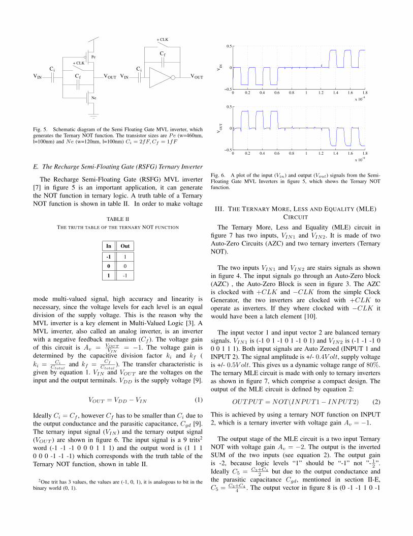
Pe
Ne
C
IN VV OUT
i
VOUT
iC
INV
fC
Cf
+ CLK
+ CLK
Fig. 5. Schematic diagram of the Semi Floating Gate MVL inverter, whichgenerates the Ternary NOT function. The transistor sizes are Pe (w=460nm,l=100nm) and Ne (w=120nm, l=100nm) Ci = 2fF, Cf = 1fF
E. The Recharge Semi-Floating Gate (RSFG) Ternary Inverter
The Recharge Semi-Floating Gate (RSFG) MVL inverter[7] in figure 5 is an important application, it can generatethe NOT function in ternary logic. A truth table of a TernaryNOT function is shown in table II. In order to make voltage
TABLE II
THE TRUTH TABLE OF THE TERNARY NOT FUNCTION
In Out
-1 1
0 0
1 -1
mode multi-valued signal, high accuracy and linearity isnecessary, since the voltage levels for each level is an equaldivision of the supply voltage. This is the reason why theMVL inverter is a key element in Multi-Valued Logic [3]. AMVL inverter, also called an analog inverter, is an inverterwith a negative feedback mechanism (Cf ). The voltage gainof this circuit is Av = VOUT
VIN= −1. The voltage gain is
determined by the capacitive division factor ki and kf (ki = Ci
Ctotaland kf = Cf
Ctotal). The transfer characteristic is
given by equation 1. VIN and VOUT are the voltages on theinput and the output terminals. VDD is the supply voltage [9].
VOUT = VDD − VIN (1)
Ideally Ci = Cf , however Cf has to be smaller than Ci due tothe output conductance and the parasitic capacitance, Cgd [9].The ternary input signal (VIN ) and the ternary output signal(VOUT ) are shown in figure 6. The input signal is a 9 trits2
word (-1 -1 -1 0 0 0 1 1 1) and the output word is (1 1 10 0 0 -1 -1 -1) which corresponds with the truth table of theTernary NOT function, shown in table II.
2One trit has 3 values, the values are (-1, 0, 1), it is analogous to bit in thebinary world (0, 1).
0 0.2 0.4 0.6 0.8 1 1.2 1.4 1.6 1.8
x 10−8
−0.5
0
0.5
VIN
0 0.2 0.4 0.6 0.8 1 1.2 1.4 1.6 1.8
x 10−8
−0.5
0
0.5
VO
UT
Fig. 6. A plot of the input (Vin) and output (Vout) signals from the Semi-Floating Gate MVL Inverters in figure 5, which shows the Ternary NOTfunction.
III. THE TERNARY MORE, LESS AND EQUALITY (MLE)CIRCUIT
The Ternary More, Less and Equality (MLE) circuit infigure 7 has two inputs, VIN1 and VIN2. It is made of twoAuto-Zero Circuits (AZC) and two ternary inverters (TernaryNOT).
The two inputs VIN1 and VIN2 are stairs signals as shownin figure 4. The input signals go through an Auto-Zero block(AZC) , the Auto-Zero Block is seen in figure 3. The AZCis clocked with +CLK and −CLK from the simple ClockGenerator, the two inverters are clocked with +CLK tooperate as inverters. If they where clocked with −CLK itwould have been a latch element [10].
The input vector 1 and input vector 2 are balanced ternarysignals. VIN1 is (-1 0 1 -1 0 1 -1 0 1) and VIN2 is (-1 -1 -1 00 0 1 1 1). Both input signals are Auto Zeroed (INPUT 1 andINPUT 2). The signal amplitude is +/- 0.4V olt, supply voltageis +/- 0.5V olt. This gives us a dynamic voltage range of 80%.The ternary MLE circuit is made with only to ternary invertersas shown in figure 7, which comprise a compact design. Theoutput of the MLE circuit is defined by equation 2:
OUTPUT = NOT (INPUT1 − INPUT2) (2)
This is achieved by using a ternary NOT function on INPUT2, which is a ternary inverter with voltage gain Av = −1.
The output stage of the MLE circuit is a two input TernaryNOT with voltage gain Av = −2. The output is the invertedSUM of the two inputs (see equation 2). The output gainis -2, because logic levels “1” should be “-1” not ”- 1
2”.Ideally C5 = C3+C4
2 but due to the output conductance andthe parasitic capacitance Cgd, mentioned in section II-E,C5 = C3+C4
4 . The output vector in figure 8 is (0 -1 -1 1 0 -1

1 1 0) which verifies the truth table of the presented MLEcircuit shown in table I.
The logic levels at the output, (see figure 9), are within theirboundaries. The boundaries for logic level “-1” are between-500mV and -300mV. Logic level “0” is defined when theboundaries are -150mV to 150mV, and for logic level “1”it is 300mV to 500mV. This means if the output signal iswithin these boundaries, the logic levels are recognized. If theoutput signal are between 150mV to 300mV and -300mV to -150mV the signal is undefined. In order to have a well-definedbalanced ternary signal, the output signal can be refreshedusing a Ternary Switching Element [8]. After the refreshingelement the signal will be in the middle of their boundaries.
V
C4
C5
C3
OUTPUT
INPUT 2
INPUT 1
INPUT 2 INV
AZC
AZC
C1
C2
+ CLK
+ CLK
+ CLK
− CLK
− CLK
+ CLK
IN 2V
IN 1
Fig. 7. Schematic diagram of the Ternary More, Less and Equality (MLE)circuit. The transistor sizes are Pe (w=460nm, l=100nm) and Ne (w=120nm,l=100nm), C2, C5 = 1fF and C1, C3, C4 = 2fF .
0 0.2 0.4 0.6 0.8 1 1.2 1.4 1.6 1.8
x 10−8
−0.5
0
0.5
INP
UT
1
0 0.2 0.4 0.6 0.8 1 1.2 1.4 1.6 1.8
x 10−8
−0.5
0
0.5
INP
UT
2
0 0.2 0.4 0.6 0.8 1 1.2 1.4 1.6 1.8
x 10−8
−0.5
0
0.5
INP
UT
2 IN
V
0 0.2 0.4 0.6 0.8 1 1.2 1.4 1.6 1.8
x 10−8
−0.5
0
0.5
OU
TP
UT
Fig. 8. A plot of the input and output signal from the More, Less andEquality (MLE) Circuit in figure 7.
IV. CONCLUSIONS
In this paper a novel ternary More, Less and Equality(MLE) Circuit has been presented. It has a compact designwith only two ternary inverters. It operates with a clockfrequency at 1 GHz. The total power dissipation is less than200µWatt, including the Auto Zero Circuit and the Simple
0 0.2 0.4 0.6 0.8 1 1.2 1.4 1.6 1.8
x 10−8
−0.5
−0.4
−0.3
−0.2
−0.1
0
0.1
0.2
0.3
0.4
0.5
1
0
−1
Fig. 9. The noise margins, which shows the boundaries for the logic levels.
Clock Generator. The supply voltage is only +/- 0.5 Volt.This circuit is a fundamental building block in a fast ternarysearch tree structure.
The More, Less and Equality (MLE) Circuit has been evalu-ated with Cadence R©Analog Design Environment, by using theCMOS090 GP process parameters from STMicroelectronics,this is a 90nm General Purpose Bulk CMOS Process with 7metal layers. All capacitors are metal plate capacitors, basedon a vertical coupling capacitance between stacked metalplates.
REFERENCES
[1] B. Hayes, “Third Base,” American Scientist, Volume 89, Number 6, pp.490–494, Nov-Dec 2001.
[2] D. Knuth, The Art of Computer Programming, Second edition. Addison-Wesley Publishing Company, 1981.
[3] Y. Berg, S. Aunet, O. Mirmotahari, and M. Høvin, “Novel RechargeSemi-Floating-Gate CMOS Logic For Multiple-Valued Systems,” Pro-ceedings of the 2003 IEEE International Symposium on Circuits AndSystems in Bangkok, 2003.
[4] T. Shibata and T. Ohmi, “A Functional MOS Transistor Featuring Gate-Level Weighted Sum and Threshold Operations,” IEEE Transactions onElectron devices, vol. 39(6), pp. 1444–1455, 1992.
[5] K. Kotani, T. Shibata, M. Imai, and T. Ohmi, “Clocked Neuron-MOS Logic Circuits Employing Auto Threhold Adjustment,” IEEEInternational Solid-State Circuits Conference(ISSCC), pp. 320–321,388,1995.
[6] Y. Berg, S. Aunet, Ø. Næss, O. Mirmotahari, and M. Høvin, “Binary toMultiple-Valued Recharge Converter for Multiple-Valued CMOS logic,”ECCTD’03-Euopean Conference on Circuit Theory and Design,Cracow,Poland, pp. 349–352, 2003.
[7] H. Gundersen and Y. Berg, “MAX and MIN Functions Using Multiple-Valued Recharge Semi-Floating Gate Circuits,” Proceedings of the 2004IEEE International Symposium on Circuits And Systems in Vancouver,2004.
[8] Y. Berg and H. Gundersen, “A Novel Ternary Switching Element UsingCMOS Recharge Semi-Floating Gate Devices,” Proceedings of the 35thIEEE International Symposium on Multiple-Valued Logic in Calgary,pp. 54 –58, May. 2005.
[9] Y. Berg, T. S. Lande, Ø. Næss, and H. Gundersen, “Ultra-Low-VoltageFloating Gate Transconductance Amplifiers,” IEEE Trans. Circuits andSystems-II: Analog and Digital Signal Processing,vol.48,no.1, Jan. 2001.
[10] O. Mirmotahari and Y. Berg, “A Novel D-Latch in Multiple-ValuedSemi-Floating-Gate Recharged Logic,” Proceedings of the 34th IEEEInternational Symposium on Multiple-Valued Logic in Tokyo, pp. 135–138, 2003.

7.4 PAPER IV: Fault Tolerant CMOS Logic UsingTernary Gates
Yngvar Berg, Rene Jensen, Johannes Lomsdalen, Henning Gundersen and Snorre AunetDepartment of informatics, University of Oslo
Proceedings of 37th International Symposium on Multiple-Valued Logic,ISMVL, Oslo Norway, May 14-15, 2007,
ISBN 0-7695-2831-1
71

72

Fault tolerant CMOS logic using ternary gates.
Yngvar Berg, Rene Jensen, Johannes Lomsdalen, Henning GundersenSnorre Aunet
Microelectronic SystemsDepartment of Informatics
University of OsloOslo, Norway
Email: [email protected]
Abstract
In this paper we present fault tolerant CMOS logic usingredundancy and ternary signals. The ternary gates are im-plemented using recharge logic which can be exploited inbinary and multiple-valued logic (MVL). Signals are pro-cessed through capacitors in such a way that the logic op-eration of a gate is independent of the DC voltage appliedon the inputs. By combining signals through capacitorsstuck on/stuck off and stuck at faults are not destructivewhen redundancy is applied. Simulated data for 130nmand 0.35µm CMOS processes are given.
1 Introduction
The technology trend introduces a wide variety of prob-lems related to reliability of circuits. The ever increased in-tegration of devices on a single die raises the probability oferroneous components in the die. The increasing probabil-ity of faults in a circuit increase the demand of fault tolerantlogic. The most reasonable way to overcome the reliabil-ity problems is to build fault tolerant circuits. Floating-gateCMOS[1] can be used to overcome some of the problemsdue to stuck-at failures.
In this paper we present a ternary logic gate which isfault tolerant. I section II we discuss briefly some commonfaults in CMOS circuits, and in section III we introduce asemi-floating-gate[2] (SFG) majority-3 (MAJ3) ternary in-verter which reduces the effect of faults compared to stan-dard CMOS gates. In section IV we present a fault tolerantredundant ternary SFG gate.
2 Faults and redundancy
In this section we will discuss briefly common CMOSfailures[3]. The failures considered are
• Stuck-at faults.
– Stuck at VDD (SA1). A node is assumed to bestucked at VDD independently of signal values orother failures. We assume that the node will notbe affected by currents pulling the the node to-wards gnd. The failures can be caused by defectpMOS transistor(s) pulling a node to VDD witha current larger than the ON current provided byoperative transistors.
– Stuck at gnd (SA0). A node is assumed to bestucked at gnd independently of signal values orother failures. We assume that the node will notbe affected by currents pulling the the node to-wards VDD.
• Stuck-open faults.
– MOSFET stuck-open (SOFF). A transistor thatcan not be turned on, is assumed to deliver a min-imum current given by the OFF state of a transis-tor.
– Interconnect stuck-open (IOFF). Floatingnodes. Normally modelled by unconnected tran-sistor terminals. An unconnected gate terminalmay be equivalent to a SOFF or even a SONfailure.
• Stuck-closed faults.
– MOSFET stuck-closed (SON). A transistor thatcan not be turned off, is assumed to deliver amaximum current given by the ON state of a tran-sistor.
Proceedings of the 37th International Symposium on Multiple-Valued Logic (ISMVL'07)0-7695-2831-7/07 $20.00 © 2007
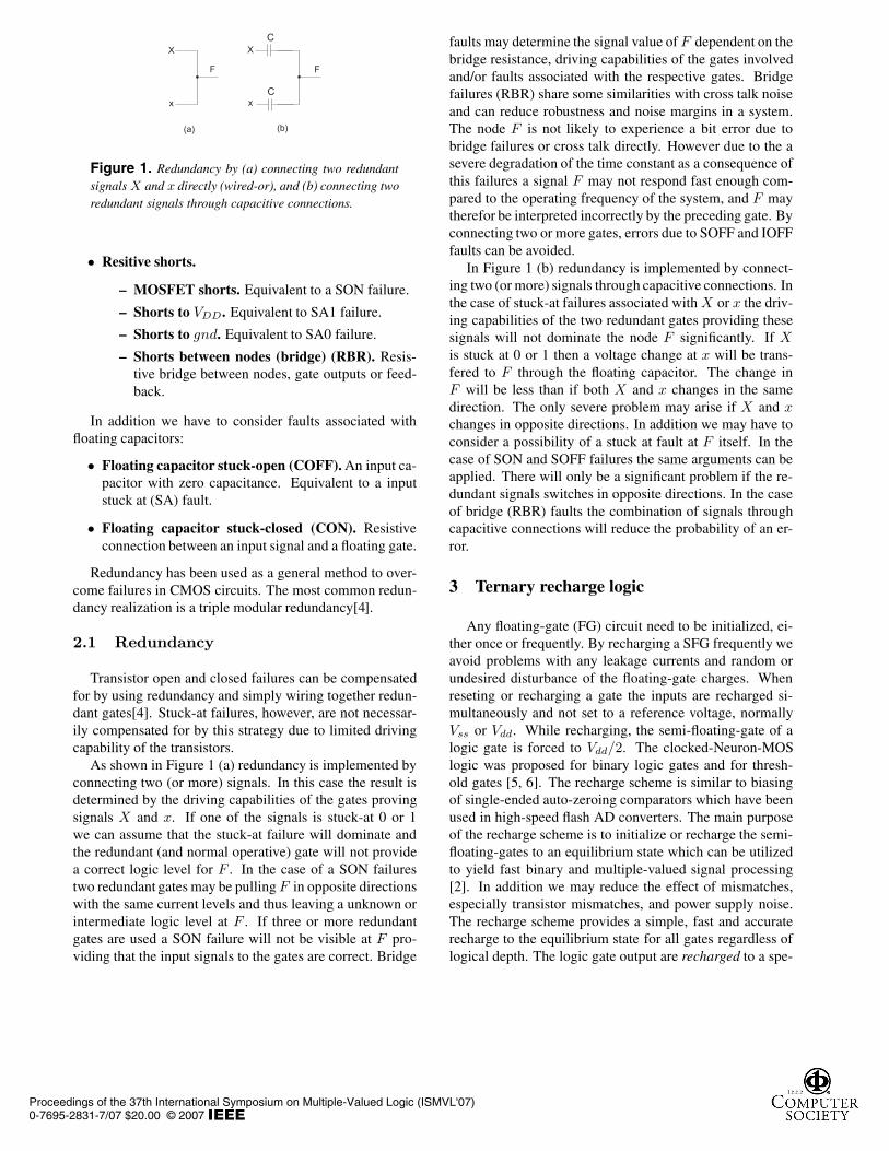
X
x
X
x
C
C
F F
(a) (b)
Figure 1. Redundancy by (a) connecting two redundantsignals X and x directly (wired-or), and (b) connecting tworedundant signals through capacitive connections.
• Resitive shorts.
– MOSFET shorts. Equivalent to a SON failure.
– Shorts to VDD. Equivalent to SA1 failure.
– Shorts to gnd. Equivalent to SA0 failure.
– Shorts between nodes (bridge) (RBR). Resis-tive bridge between nodes, gate outputs or feed-back.
In addition we have to consider faults associated withfloating capacitors:
• Floating capacitor stuck-open (COFF). An input ca-pacitor with zero capacitance. Equivalent to a inputstuck at (SA) fault.
• Floating capacitor stuck-closed (CON). Resistiveconnection between an input signal and a floating gate.
Redundancy has been used as a general method to over-come failures in CMOS circuits. The most common redun-dancy realization is a triple modular redundancy[4].
2.1 Redundancy
Transistor open and closed failures can be compensatedfor by using redundancy and simply wiring together redun-dant gates[4]. Stuck-at failures, however, are not necessar-ily compensated for by this strategy due to limited drivingcapability of the transistors.
As shown in Figure 1 (a) redundancy is implemented byconnecting two (or more) signals. In this case the result isdetermined by the driving capabilities of the gates provingsignals X and x. If one of the signals is stuck-at 0 or 1we can assume that the stuck-at failure will dominate andthe redundant (and normal operative) gate will not providea correct logic level for F . In the case of a SON failurestwo redundant gates may be pulling F in opposite directionswith the same current levels and thus leaving a unknown orintermediate logic level at F . If three or more redundantgates are used a SON failure will not be visible at F pro-viding that the input signals to the gates are correct. Bridge
faults may determine the signal value of F dependent on thebridge resistance, driving capabilities of the gates involvedand/or faults associated with the respective gates. Bridgefailures (RBR) share some similarities with cross talk noiseand can reduce robustness and noise margins in a system.The node F is not likely to experience a bit error due tobridge failures or cross talk directly. However due to the asevere degradation of the time constant as a consequence ofthis failures a signal F may not respond fast enough com-pared to the operating frequency of the system, and F maytherefor be interpreted incorrectly by the preceding gate. Byconnecting two or more gates, errors due to SOFF and IOFFfaults can be avoided.
In Figure 1 (b) redundancy is implemented by connect-ing two (or more) signals through capacitive connections. Inthe case of stuck-at failures associated with X or x the driv-ing capabilities of the two redundant gates providing thesesignals will not dominate the node F significantly. If Xis stuck at 0 or 1 then a voltage change at x will be trans-fered to F through the floating capacitor. The change inF will be less than if both X and x changes in the samedirection. The only severe problem may arise if X and xchanges in opposite directions. In addition we may have toconsider a possibility of a stuck at fault at F itself. In thecase of SON and SOFF failures the same arguments can beapplied. There will only be a significant problem if the re-dundant signals switches in opposite directions. In the caseof bridge (RBR) faults the combination of signals throughcapacitive connections will reduce the probability of an er-ror.
3 Ternary recharge logic
Any floating-gate (FG) circuit need to be initialized, ei-ther once or frequently. By recharging a SFG frequently weavoid problems with any leakage currents and random orundesired disturbance of the floating-gate charges. Whenreseting or recharging a gate the inputs are recharged si-multaneously and not set to a reference voltage, normallyVss or Vdd. While recharging, the semi-floating-gate of alogic gate is forced to Vdd/2. The clocked-Neuron-MOSlogic was proposed for binary logic gates and for thresh-old gates [5, 6]. The recharge scheme is similar to biasingof single-ended auto-zeroing comparators which have beenused in high-speed flash AD converters. The main purposeof the recharge scheme is to initialize or recharge the semi-floating-gates to an equilibrium state which can be utilizedto yield fast binary and multiple-valued signal processing[2]. In addition we may reduce the effect of mismatches,especially transistor mismatches, and power supply noise.The recharge scheme provides a simple, fast and accuraterecharge to the equilibrium state for all gates regardless oflogical depth. The logic gate output are recharged to a spe-
Proceedings of the 37th International Symposium on Multiple-Valued Logic (ISMVL'07)0-7695-2831-7/07 $20.00 © 2007
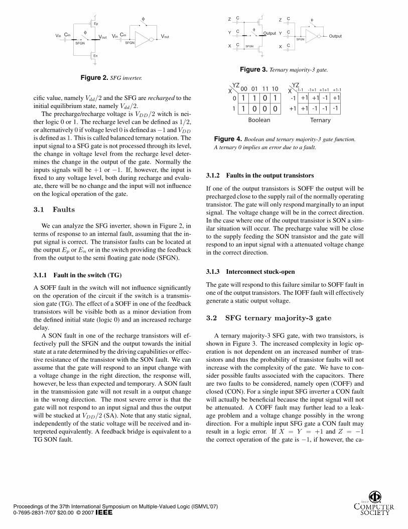
VinVout Voutφ
φ
Cin Cin
SFGN SFGN
Ep
En
Vin
Figure 2. SFG inverter.
cific value, namely Vdd/2 and the SFG are recharged to theinitial equilibrium state, namely Vdd/2.
The precharge/recharge voltage is VDD/2 witch is nei-ther logic 0 or 1. The recharge level can be defined as 1/2,or alternatively 0 if voltage level 0 is defined as −1 and VDD
is defined as 1. This is called balanced ternary notation. Theinput signal to a SFG gate is not processed through its level,the change in voltage level from the recharge level deter-mines the change in the output of the gate. Normally theinputs signals will be +1 or −1. If, however, the input isfixed to any voltage level, both during recharge and evalu-ate, there will be no change and the input will not influenceon the logical operation of the gate.
3.1 Faults
We can analyze the SFG inverter, shown in Figure 2, interms of response to an internal fault, assuming that the in-put signal is correct. The transistor faults can be located atthe output Ep or En or in the switch providing the feedbackfrom the output to the semi floating gate node (SFGN).
3.1.1 Fault in the switch (TG)
A SOFF fault in the switch will not influence significantlyon the operation of the circuit if the switch is a transmis-sion gate (TG). The effect of a SOFF in one of the feedbacktransistors will be visible both as a minor deviation fromthe defined initial state (logic 0) and an increased rechargedelay.
A SON fault in one of the recharge transistors will ef-fectively pull the SFGN and the output towards the initialstate at a rate determined by the driving capabilities or effec-tive resistance of the transistor with the SON fault. We canassume that the gate will respond to an input change witha voltage change in the right direction, the response will,however, be less than expected and temporary. A SON faultin the transmission gate will not result in a output changein the wrong direction. The most severe error is that thegate will not respond to an input signal and thus the outputwill be stucked at VDD/2 (SA). Note that any static signal,independently of the static voltage will be received and in-terpreted equivalently. A feedback bridge is equivalent to aTG SON fault.
Y OutputφC
SFGN
Z C
X C
Y CSFGN
Z C
X C
φ
Output
Figure 3. Ternary majority-3 gate.
0
1
XYZ
00 01 11 10
0 0 00
11 1 1 -1
+1
XYZ
-1-1 -1+1 +1+1 +1-1
-1 -1 -1
-1
+1
+1 +1 +1
Boolean Ternary
Figure 4. Boolean and ternary majority-3 gate function.A ternary 0 implies an error due to a fault.
3.1.2 Faults in the output transistors
If one of the output transistors is SOFF the output will beprecharged close to the supply rail of the normally operatingtransistor. The gate will only respond marginally to an inputsignal. The voltage change will be in the correct direction.In the case where one of the output transistor is SON a sim-ilar situation will occur. The precharge value will be closeto the supply feeding the SON transistor and the gate willrespond to an input signal with a attenuated voltage changein the correct direction.
3.1.3 Interconnect stuck-open
The gate will respond to this failure similar to SOFF fault inone of the output transistors. The IOFF fault will effectivelygenerate a static output voltage.
3.2 SFG ternary majority-3 gate
A ternary majority-3 SFG gate, with two transistors, isshown in Figure 3. The increased complexity in logic op-eration is not dependent on an increased number of tran-sistors and thus the probability of transistor faults will notincrease with the complexity of the gate. We have to con-sider possible faults associated with the capacitors. Thereare two faults to be considered, namely open (COFF) andclosed (CON). For a single input SFG inverter a CON faultwill actually be beneficial because the input signal will notbe attenuated. A COFF fault may further lead to a leak-age problem and a voltage change possibly in the wrongdirection. For a multiple input SFG gate a CON fault mayresult in a logic error. If X = Y = +1 and Z = −1the correct operation of the gate is −1, if however, the ca-
Proceedings of the 37th International Symposium on Multiple-Valued Logic (ISMVL'07)0-7695-2831-7/07 $20.00 © 2007
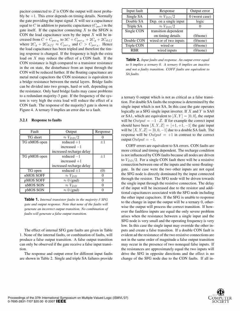
pacitor connected to Z is CON the output will most proba-bly be +1. This error depends on timing details. Normallythe gate providing the input signal X will see a capacitanceequal to C in addition to parasitic capacitance (Cpar) in thegate itself. If the capacitor connecting X to the SFGN isCON the load capacitance seen by the input X will be in-creased from C + CparX to 3C + CparX + 2Cg + 2Cdiff
where 2Cg + 2Cdiff ≈ CparX and C > CparX . Hencethe load capacitance has been tripled and therefore the tim-ing response is changed. If the frequency is high the extraload on X may reduce the effect of a CON fault. If theCON resistance is high compared to a transistor resistancein the on state, the disturbance from an input through theCON will be reduced further. If the floating capacitance aremetal metal capacitors the CON resistance is equivalent toa bridge resistance between the metal layers. Bridge faultscan be divided into two groups, hard or soft, depending onthe resistance. Only hard bridge faults may cause problemsto a redundant majority-3 gate. If the frequency of the sys-tem is very high the extra load will reduce the effect of aCON fault. The response of the majority3 gate is shown inFigure 4. A ternary 0 implies an error due to a fault.
3.2.1 Response to faults
Fault Output Response
TG short ≈ VDD/2 0TG nMOS open reduced +1 ±1
increased −1increased recharge delay
TG pMOS open reduced −1 ±1increased +1
increased recharge delayTG open reduced ±1 (0)
nMOS SOFF ≈ VDD 0pMOS SOFF ≈ 0 (gnd) 0nMOS SON ≈ VDD 0pMOS SON ≈ 0 (gnd) 0
Table 1. Internal transistor faults in the majority-3 SFGgate and output response. Note that none of the faults willgenerate an incorrect output transition. No combination offaults will generate a false output transition.
The effect of internal SFG gate faults are given in Table1. None of the internal faults, or combination of faults, willproduce a false output transition. A false output transitioncan only be observed if the gate receive a false input transi-tion.
The response and output error for different input faultsare shown in Table 2. Single and triple SA failures provide
Input fault Response Output error
Single SA ≈ VDD/2 0 (worst case)Double SA Dep. on a single input logicTriple SA ≈ VDD/2 0
Single CON transition dependenton timing details (0/none)
Double CON wired or of two inputs (0/none)Triple CON wired or (0/none)
RBR wired inputs (0/none)
Table 2. Input faults and response. An output error equalto 0 implies a ternary 0. A ternary 0 implies an inactiveand not a faulty transition. COFF faults are equivalent toSA faults.
a ternary 0 output which is not as critical as a false transi-tion. For double SA faults the response is determined by thesingle input which is not SA. In this case the gate operateslogically as a SFG single input inverter. If X and Y is SA0or SA1, which are equivalent to [X, Y ] = [0, 0], the outputwill be Output = −1 · Z . If for example the correct inputshould have been [X, Y, Z] = [+1, +1,−1] the gate inputwill be [X, Y, Z] = [0, 0,−1] due to a double SA fault. Theresponse will be Output = +1 in contrast to the correctoutput Output = −1.
COFF errors are equivalent to SA errors. CON faults aremore critical and timing dependent. The recharge conditionis not influenced by CON faults because all nodes are drivento VDD/2. For a single CON fault there will be a resistiveconnection between one of the inputs and the semi-floating-gate. In the case were the two other inputs are not equalthe SFG node is directly dominated by the input connectedthrough the resistor. The SFG node will be driven towardsthe single input through the resistive connection. The delayof the input will be increased due to the resistor and addi-tional capacitances associated with the SFG node includingthe other input capacitors. If the SFG is unable to responseto the change in input the output will be a ternary 0, other-wise the output will process the correct transition. If how-ever the faultless inputs are equal the only severe problemarises when the resistance between a single input and theSFG node is very small and the operating frequency is verylow. In this case the single input may override the other in-puts and create a false transition. If a double CON fault isevident ad the resistance of the two resistive connections arenot in the same order of magnitude a false output transitionmay occur in the presence of two nonequal false inputs. Ifthe resistances are approximately equal the two inputs willdrive the SFG in opposite directions and the effect is nochange of the SFG node due to the CON faults. If all in-
Proceedings of the 37th International Symposium on Multiple-Valued Logic (ISMVL'07)0-7695-2831-7/07 $20.00 © 2007
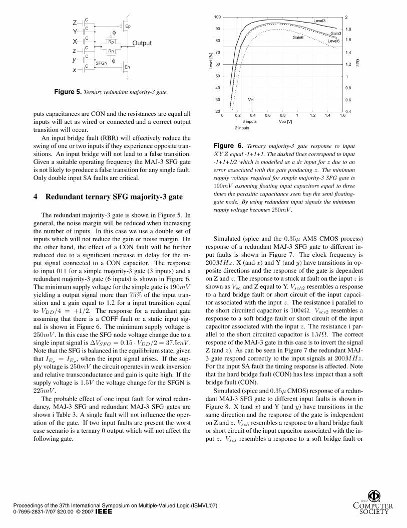
Y
Output
φ
C
SFGN
Z C
X Cφ
y Cz C
x C
Rp
Rn
Ep
En
Figure 5. Ternary redundant majority-3 gate.
puts capacitances are CON and the resistances are equal allinputs will act as wired or connected and a correct outputtransition will occur.
An input bridge fault (RBR) will effectively reduce theswing of one or two inputs if they experience opposite tran-sitions. An input bridge will not lead to a false transition.Given a suitable operating frequency the MAJ-3 SFG gateis not likely to produce a false transition for any single fault.Only double input SA faults are critical.
4 Redundant ternary SFG majority-3 gate
The redundant majority-3 gate is shown in Figure 5. Ingeneral, the noise margin will be reduced when increasingthe number of inputs. In this case we use a double set ofinputs which will not reduce the gain or noise margin. Onthe other hand, the effect of a CON fault will be furtherreduced due to a significant increase in delay for the in-put signal connected to a CON capacitor. The responseto input 011 for a simple majority-3 gate (3 inputs) and aredundant majority-3 gate (6 inputs) is shown in Figure 6.The minimum supply voltage for the simple gate is 190mVyielding a output signal more than 75% of the input tran-sition and a gain equal to 1.2 for a input transition equalto VDD/4 = +1/2. The response for a redundant gateassuming that there is a COFF fault or a static input sig-nal is shown in Figure 6. The minimum supply voltage is250mV . In this case the SFG node voltage change due to asingle input signal is ∆VSFG = 0.15 · VDD/2 = 37.5mV .Note that the SFG is balanced in the equilibrium state, giventhat IEp = IEp , when the input signal arises. If the sup-ply voltage is 250mV the circuit operates in weak inversionand relative transconductance and gain is quite high. If thesupply voltage is 1.5V the voltage change for the SFGN is225mV .
The probable effect of one input fault for wired redun-dancy, MAJ-3 SFG and redundant MAJ-3 SFG gates areshown i Table 3. A single fault will not influence the oper-ation of the gate. If two input faults are present the worstcase scenario is a ternary 0 output which will not affect thefollowing gate.
0 0.2 0.4 0.6 0.8 1 1.2 1.4 1.620
30
40
50
60
70
80
90
100
VDD [V]
Leve
l [%
]
0.4
0.6
0.8
1.2
1.4
1.6
1.8
1
2
Gain3Gain6
Level6
Level3
6 inputs2 inputs
Vth
Gain
Figure 6. Ternary majority-3 gate response to inputXY Z equal -1+1+1. The dashed lines correspond to input-1+1+1/2 which is modelled as a dc input for z due to anerror associated with the gate producing z. The minimumsupply voltage required for simple majority-3 SFG gate is190mV assuming floating input capacitors equal to threetimes the parasitic capacitance seen bay the semi floating-gate node. By using redundant input signals the minimumsupply voltage becomes 250mV .
Simulated (spice and the 0.35µ AMS CMOS process)response of a redundant MAJ-3 SFG gate to different in-put faults is shown in Figure 7. The clock frequency is200MHz. X (and x) and Y (and y) have transitions in op-posite directions and the response of the gate is dependenton Z and z. The response to a stuck at fault on the input z isshown as Vsa and Z equal to Y. Vsch2 resembles a responseto a hard bridge fault or short circuit of the input capaci-tor associated with the input z. The resistance i parallel tothe short circuited capacitor is 100kΩ. Vscs2 resembles aresponse to a soft bridge fault or short circuit of the inputcapacitor associated with the input z. The resistance i par-allel to the short circuited capacitor is 1MΩ. The correctrespone of the MAJ-3 gate in this case is to invert the signalZ (and z). As can be seen in Figure 7 the redundant MAJ-3 gate respond correctly to the input signals at 200MHz.For the input SA fault the timing response is affected. Notethat the hard bridge fault (CON) has less impact than a softbridge fault (CON).
Simulated (spice and 0.35µ CMOS) response of a redun-dant MAJ-3 SFG gate to different input faults is shown inFigure 8. X (and x) and Y (and y) have transitions in thesame direction and the response of the gate is independenton Z and z. Vsch resembles a response to a hard bridge faultor short circuit of the input capacitor associated with the in-put z. Vscs resembles a response to a soft bridge fault or
Proceedings of the 37th International Symposium on Multiple-Valued Logic (ISMVL'07)0-7695-2831-7/07 $20.00 © 2007

0 2 4 6 8 10 120
1
2
Y a
nd y
0 2 4 6 8 10 120
1
2
X a
nd x
0 2 4 6 8 10 120
1
2
Vsa
0 2 4 6 8 10 120
1
2
Vsc
h2
0 2 4 6 8 10 120
1
2
Vsc
s2
Time [ns]
0 2 4 6 8 10 120
1
2
Z an
d (z)
Figure 7. Simulated (spice and the 0.35µ AMS CMOSprocess) response of a redundant MAJ-3 SFG gate to dif-ferent input faults.
0 2 4 6 8 10 120
1
2
Z an
d z
0 2 4 6 8 10 120
1
2
X a
nd x
Y an
d y
0 2 4 6 8 10 120
1
2
Vsc
h
0 2 4 6 8 10 120
1
2
Vsc
s
Figure 8. Simulated (spice and 0.35µ CMOS) responseof a redundant MAJ-3 SFG gate to different input faults.
Inp. fault Wired err. MAJ-3 error Red. MAJ-3 err.
SA logic 0 noneRBR logic (logic) noneIOFF none 0 noneCOFF logic noneCON logic none
Table 3. The probable effect of one input fault for wiredredundancy, MAJ-3 SFG and redundant MAJ-3 SFG gates.
short circuit of the input capacitor associated with the in-put z. Given the inputs X= x =Y= y, the response of theredundant MAJ-3 gate should be unaffected by the thrirdinput Z and z. Given a clock frequency of 200MHz thecircuit operates correctly. In this case the circuit is less af-fected by a soft CON fault than by a hard CON fault.
5 Conclusion
In this paper we presented fault tolerant CMOS logicusing redundancy and ternary signals. Signals are pro-cessed through capacitors in such a way that the logic oper-ation of a gate is independent of the DC voltage applied onthe inputs. By combining signals through capacitors stuckon/stuck off and stuck at faults are not destructive when re-dundancy is applied.
References
[1] T. Shibata and T. Ohmi. “ A Functional MOS Transistor Fea-turing Gate-Level Weighted Sum and Threshold Operations”,In IEEE Transactions on Electron Devices, vol 39, 1992.
[2] Y. Berg, S. Aunet, Ø. Næss and O. Mirmotahari. “BasicMultiple-Valued Functions Using Recharge CMOS Logic”,Proceedings, 34th Int. Symposium on Multiple-Valued Logic,2004 .
[3] C. Constantinescu. “Trends and challanges in VLSI circuit re-liability”, IEEE Micro, Volume: 23, Issue: 4, July-Aug. 2003.
[4] B.W. Johnson. “Design and Analysis of Fault-Tolerant DigitalSystems”, Addison-Wesley Publishing Compant 1989, ISBN0-201-07570-9.
[5] K. Kotani, T. Shibata, M. Imai and T. Ohmi. “Clocked-Neuron-MOS Logic Circuits Employing Auto-Threshold-Adjustment”, In IEEE International Solid-State Circuits Con-ference (ISSCC), pp. 320-321,388, 1995.
[6] R. Lashevsky, K. Takaara and M. Souma “Neuron MOSFETas a Way to Design a Threshold Gates with the Threshold andInput Weights Alterable in Real Time”, IEEE TT13.11-1.4,1998, pp. 263–266.
Proceedings of the 37th International Symposium on Multiple-Valued Logic (ISMVL'07)0-7695-2831-7/07 $20.00 © 2007
7.5 PAPER V: A Novel Balanced Ternary Adder UsingRecharged Semi-Floating Gate Devices
Henning Gundersen and Yngvar BergDepartment of informatics, University of Oslo
Proceedings of 36th International Symposium on Multiple-Valued Logic,ISMVL, Singapore May 17-20, 2006,
ISBN 0-7695-2532-6
79

80

A Novel Balanced Ternary Adder Using RechargedSemi-Floating Gate Devices
Henning Gundersen and Yngvar BergDepartment of Informatics, Microelectronic Systems Group, University of Oslo
Blindern, NO-0316, Oslo, NorwayEmail: [email protected]
Abstract— This paper presents a novel voltage mode Bal-anced Ternary Adder (BTA), implemented with Recharged Semi-Floating Gate Devices. By using balanced ternary notation, it pos-sible to take advantage of carry free addition, which is exploitedin designing a fast adder cell. The circuit operates at 1 GHzclock frequency. The supply voltage is only 1.0 Volt. The circuit issimulated by using Cadence R©Analog Design Environment, withCMOS090 process parameters, a 90nm General Purpose BulkCMOS Process from STMicroelectronics with 7 metal layers.All the capacitors are metal plate capacitors, based on verticalcoupling capacitance between stacked metal plates.
I. INTRODUCTION
Humans count by tens, machines count by twos, thissums up the way we do arithmetic today. However, thereare countless other ways to count. This paper will presenta ternary adder which uses base 3 representation. ’Ternarynumbering systems is the most efficient of all integer bases’as Brian Hayes claims in his article Third Base[1]. Ternarynumber systems use number representation with radix=3,compared with binary, which uses radix=2. Another wayof representing a ternary number is by using a balancedternary notation. ’Perhaps the prettiest number system ofall’ as Donald Knuth said in his book, The Art of ComputerProgramming [2]. In the balanced ternary the digits are alsopowers of 3, as in ordinary ternary numbers, but they are’balanced’ since they are symmetrical about zero. Anotherapproach by using ternary logic in fast adder design, ispresented by Rajashekhara et.al. [3]
A given example of a balanced ternary number is thedecimal number 23. It is written in balanced ternarynotation as: 1011. This numeral is interpreted as:1x33 + 0x32 − 1x31 − 1x30, or 27 + 0 - 3 - 1, indecimal notation. The balanced ternary number system hasalso some nice properties:a) Negation is easy, change 1 with 1, and vica versa. If weuse the example -23, the result will be 1011 in balancedternary notation.b) The sign of a number is given by its most significantnonzero ’trit1’c) The operation of rounding to the nearest integer is identicalto truncation.
1One trit has 3 values, the values are (-1, 0, 1), it is analogous to bit in thebinary world (0 , 1).
d) Addition and subtraction are essentially the same operation:just negate one number, and afterwards do an adding operation.
The multiple-input Floating-Gate (FG) transistors can beused to simplify the design of multiple-valued logic [4]. Theinitial charge on the floating-gates may vary significantlyand therefore impose a very severe inaccuracy, unless we doapply some form of initialization. Research on floating-gatereset strategies have been presented by Kotani et.al. [5], andby Berg et.al. [6].
Floating-Gate (FG) circuits need to be initialized, eitheronce initially or frequently. The once and for all initializationis synonymous with programming. By recharging the FGfrequently we avoid problems with any leakage currentsand random or undesired disturbance of the floating-gatecharges, and we convert the non-volatile floating gates toSemi Floating-Gates (SFG)[6]. The reset or recharged schememay be used to overcome some problems associated withthe floating-gate circuit design. The recharged conditionis different than the reset in clocked-Neuron-MOS logicproposed by Kotani et.al. [5].
When reseting or recharging a gate the inputs are rechargedsimultaneously and are not set to a reference voltage. Whilerecharging, the gates are short-circuited using a local rechargeswitch (+Clk), the output and the semi floating-gate on theinput is forced to Vdd/2, see figure 1.
The recharged scheme is similar to biasing of single-endedauto-zeroing comparators, which have been used in high-speed flash AD converters. The main purpose of the rechargedscheme is to initialize or recharge the semi-floating-gates to anequilibrium state which can be utilized to yield fast binary andmultiple-valued signal processing. In addition we may reducethe effect of mismatches, especially transistor mismatches,and power supply noise. The recharged scheme provides asimple, fast and accurate recharge to the equilibrium statefor all gates regardless of logical depth. We use the termRecharged Logic (RL) or Recharged Semi-Floating GateLogic (RSFGL) for the circuits presented in this paper [7].The SFG circuits are recharged to the initial equilibriumstate, namely Vdd/2.
Proceedings of the 36th International Symposium on Multiple-Valued Logic (ISMVL’06) 0-7695-2532-6/06 $20.00 © 2006 IEEE

This paper will present a novel carry free Balanced TernaryAdder (BTA) using Recharged Semi-Floating Gate (RSFG)devices. The truth table of the presented adder is shown intable I. Section II will briefly cover some of the building blocksused in Recharged Semi-Floating Gate design. In section IIIwe will look closer to the realization of the voltage modeBalanced Ternary Adder (BTA).
TABLE I
THE TRUTH TABLE OF THE BALANCED TERNARY ADDER
X 1 1 1 0 0 0 1 1 1
Y 1 0 1 1 0 1 1 0 1
SUM 11 01 00 01 00 01 00 01 11
II. FUNDAMENTAL BUILDING BLOCKS USED IN
RECHARGED SEMI-FLOATING GATE (RSFG) DESIGN
A. The Recharged Semi-Floating Gate (RSFG) Inverter
Ne
Pe
Ci + Clk
+ Clk
out outV V V Vinin
Ci
Fig. 1. Schematic diagram of a Recharged Semi-Floating Gate Inverter. Thetransistor sizes are Pe (w = 460nm and l = 100nm) and Ne (w = 120nmand l = 100nm)
A Recharged Semi-Floating Gate (RSFG) inverter is shownin figure 1. The RSFG inverter act just like a ordinary inverter,except that it has a local feedback switch (+Clk) connectedbetween the input gates and the output. By equalizing the βswe obtain an equilibrium state when the recharged signal is1, and the output and the gate are driven towards Vdd/2. Therecharge frequency is twice the frequency of the input signal.
B. The Recharged Semi-Floating Gate (RSFG) Ternary In-verter
The Recharge Semi-Floating Gate (RSFG) MVL-Inverter[8] in figure 2 is an important application. This is a keyelement in Multi-Valued Logic [6]. A MVL inverter, alsocalled an analog inverter, is an inverter with a negativefeedback mechanism, Cf [9]. The voltage gain of this circuitis Av = ΔVout
ΔVin= −1. The transfer characteristic of the analog
inverter is given by equation1.
Vout = Vdd − Vin (1)
A MVL inverter can be used to generate the NOT or theNegation function in ternary logic. A truth table of a TernaryNOT function is shown in table II.
Ci
Ne
Pe
Ci
+ Clk
+ Clk
Cf
Cf
out in outV V VinV
Fig. 2. Schematic diagram of the Recharged Semi-Floating Gate MVLInverter, which generates the Ternary NOT function. The transistor sizes arePe (w = 460nm and l = 100nm) and Ne (w = 120nm and l = 100nm)
TABLE II
THE TRUTH TABLE OF THE TERNARY NOT FUNCTION
In Out
1 1
0 0
1 1
C. The Auto-Zero Circuit (AZC)
The input stages needs an Auto-Zero Circuit (AZC) asshown in figure 3. An Auto-Zero circuit can be seen as a signalconverter which converts an input signal to a valid rechargesignal [10]. The recharge frequency is twice the frequency ofthe input signal. The AZC has two Pass-Gate Circuits, clocked
V
V
V V V− Clk
dd/2
in
out
+ Clk
in
+ Clk
+ Clk
− Clk
out
Ne
Pe
Pe
Ne
AZC
Fig. 3. Schematic diagram of the Auto-Zero circuit The transistor sizes arePe (w = 130nm and l = 100nm) and Ne (w = 130nm and l = 100nm)
with the opposite clock phase. The upper Pass-Gate Circuit infigure 3 has Vdd/2 as the input, and the lower Pass-Gate hasVin as input. The output signal Vout will then have the signallevel of Vdd/2, in the recharge period, which is set by the upperPass-Gate circuit, and Vin in the precharged period. The X andY signals shown in figure 5 are examples of Auto-Zeroed inputsignals.
Proceedings of the 36th International Symposium on Multiple-Valued Logic (ISMVL’06) 0-7695-2532-6/06 $20.00 © 2006 IEEE

+ Clk
− Clk
AZC
+ Clk
− Clk
AZC
+ Clk + Clk
+ Clk+ Clk
+ Clk + Clk+ Clk+ Clk
+ Clk + Clk
C1
C2
C3
C4
C5
C6
C9X
Y
C10
C14
C17
C15
C21
C20
C19
C18
C16
C11
i 3 i 6 i 10
i 9i 7
i 5i 2
i 1
i 8
i 4
PRE−ADDER
CARRY DETECT
SUM−CARRY
C−HIGH
C−LOW
C12
C13
SUM 1
SUM 0
C8
C7
+ Clk
− Clk
AZC
+ Clk
− Clk
AZC
Fig. 4. Schematic diagram of the Balanced Ternary Adder (C1, C2, C3, C4, C5, C6, C7, C8, C11, C12, C13, C16, C17, C20, C21 = 1fF, C9, C15 =1.5fF, C10 = 7fF, C14 = 3fF, C18 = 2fF, C19 = 4fF )
III. THE BALANCED TERNARY ADDER
A Balanced Ternary Adder (BTA) takes two Ternary inputs(X and Y) and generate the SUM output (S0 and S1), and itoffers carry free addition. The truth table of the BTA is shownin table I. The complete schematic diagram of the BalancedTernary Adder circuit is shown in figure 4.
A. The Pre-Adder stage
The Pre-Adder stage is a simple adder. The Pre-Adder addsthe two input signals X and Y electrically, using a two-inputMVL inverter. The Pre-Adder stage consists of capacitors C7,C8, C9, C10, C11 and Inverter i3 and i6. Inverter i3 is a twoinputs MVL inverter. Input signal X is connected to C7 andthe Y signal is connected to C8. The two input signals will beadded together and inverted. The output signal from i3 has tobe amplified and inverted. This is done by the ternary inverteri6, the ternary output signal from the Pre-Adder stage is shownin figure 5. The output signal of the Pre-Adder is not correct.When both X and Y is high (1) or when both X and Y are low(1), the signal has to be inverted to generate a correct SUM 0signal which correspond to the truth table I.
B. The Carry detect stage
The Carry detect stage will either detect when both X and Yis high or both X and Y is low. Furthermore this will generatea Binary high- or low-Carry signal. The Carry detect stageconsists of C1, C2, C3, C4, C5, C6 and four inverters i1, i2,i4 and i5. The main idea is to use the threshold elements i1and i2, a three input FG inverter, to detect the carry signal.To detect carry high, the three input FG inverter i1 is used.The Auto-Zeroed X is connected to C3, Auto-Zeroed Y is
connected to C2. C1 is connected to a Auto-Zeroed gnd signal.If both X and Y is high, the inverter i1 will set the outputLow, else the output will be determined by the Auto-Zeroedgnd signal, and the output of i1 will be set high. The outputwill only be set low if both X and Y is High. The logic levelsof X and Y, if they are high is = 900mV . The gnd signal is 0V. Since all of the inputs have the same weight, (C1=C2=C3)hence it will be set low only when both X and Y are 1. Carrylow detection is done in the same manner, except if both Xand Y are low, the output of inverter i2 is set high, else theoutput is set low. As figure 4 shows C4 is connected to theAuto-Zeroed Vdd and all of the input capacitors has the sameweight (C4=C5=C6). The logic levels of X and Y low (1)are 100mV and Vdd = 1.0V , hence both X and Y have tobe low to set inverter i2 high. Inverter i4 and i5 equalize andinverts the signal, the output of the Carry detect stage, C-LOWand C-HIGH is shown in figure 5. Inverter i7 is a binary toternary converter. It makes a summation of C-LOW and C-HIGH. The output signal SUM-CARRY in figure 5 is a ternaryrepresentation of the Carry signals.
C. The output stages
1) SUM 1: To generate the SUM 1 signal we only need aternary inversion of the SUM-CARRY signal, this is done bythe ternary inverter i9.
2) SUM 0: To generate SUM 0 we need to invert the PRE-ADDER output signal either when both X and Y are low orhigh at the same time. This is achieved by the two input MVLinverter i8. C14 has to be twice the value of C15 to achievethis. The output of i8 is the inverted SUM 0 signal, this is whythe output has to be inverted in inverter i10, which generate
Proceedings of the 36th International Symposium on Multiple-Valued Logic (ISMVL’06) 0-7695-2532-6/06 $20.00 © 2006 IEEE
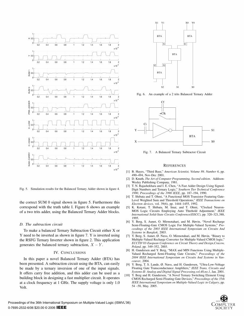
0.2 0.4 0.6 0.8 1 1.2 1.4 1.6 1.8 2
x 10−8
0
0.5
1
X
0.2 0.4 0.6 0.8 1 1.2 1.4 1.6 1.8 2
x 10−8
0
0.5
1
Y
0.2 0.4 0.6 0.8 1 1.2 1.4 1.6 1.8 2
x 10−8
0
0.5
1
SU
M 1
0.2 0.4 0.6 0.8 1 1.2 1.4 1.6 1.8 2
x 10−8
0
0.5
1
SU
M 0
0.2 0.4 0.6 0.8 1 1.2 1.4 1.6 1.8 2
x 10−8
0
0.5
1
PR
E−
AD
DE
R
0.2 0.4 0.6 0.8 1 1.2 1.4 1.6 1.8 2
x 10−8
0
0.5
1
C−
LO
W
0.2 0.4 0.6 0.8 1 1.2 1.4 1.6 1.8 2
x 10−8
0
0.5
1
C−
HIG
H
0.2 0.4 0.6 0.8 1 1.2 1.4 1.6 1.8 2
x 10−8
0
0.5
1
SU
M−
CA
RR
Y
Fig. 5. Simulation results for the Balanced Ternary Adder shown in figure 4.
the correct SUM 0 signal shown in figure 5. Furthermore thiscorrespond with the truth table I. Figure 6 shows an exampleof a two trits adder, using the Balanced Ternary Adder blocks.
D. The subtraction circuit
To make a balanced Ternary Subtraction Circuit either X orY need to be inverted as shown in figure 7. Y is inverted usingthe RSFG Ternary Inverter shown in figure 2. This applicationgenerates the balanced ternary subtraction, X − Y .
IV. CONCLUSIONS
In this paper a novel Balanced Ternary Adder (BTA) hasbeen presented. A subtraction circuit using the BTA, can easilybe made by a ternary inversion of one of the input signals.It offers carry free addition, and this adder can be used as abuilding block in designing a fast multiplier circuit. It operatesat a clock frequency at 1 GHz. The supply voltage is only 1.0Volt.
BTABTA
S1 S1
X0 Y0X1 Y1
S0
S2
S2 S1
BTA
BTA
S2
Fig. 6. An example of a 2 trits Balanced Ternary Adder
Ci
Cf
BTA
S0
S1Y
X
+Clk
Fig. 7. A Balanced Ternary Subtractor Circuit
REFERENCES
[1] B. Hayes, “Third Base,” American Scientist, Volume 89, Number 6, pp.490–494, Nov-Dec 2001.
[2] D. Knuth, The Art of Computer Programming, Second edition. Addison-Wesley Publishing Company, 1981.
[3] T. N. Rajashekhara and I. E. Chen, “A Fast Adder Design Using Signed-Digit Numbers and Ternary Logic,” Southern Tier Technical Conference1990, Proceedings of the 1990 IEEE, pp. 187–194, 1990.
[4] T. Shibata and T. Ohmi, “A Functional MOS Transistor Featuring Gate-Level Weighted Sum and Threshold Operations,” IEEE Transactions onElectron devices, vol. 39(6), pp. 1444–1455, 1992.
[5] K. Kotani, T. Shibata, M. Imai, and T. Ohmi, “Clocked Neuron-MOS Logic Circuits Employing Auto Threhold Adjustment,” IEEEInternational Solid-State Circuits Conference(ISSCC), pp. 320–321,388,1995.
[6] Y. Berg, S. Aunet, O. Mirmotahari, and M. Høvin, “Novel RechargeSemi-Floating-Gate CMOS Logic For Multiple-Valued Systems,” Pro-ceedings of the 2003 IEEE International Symposium on Circuits AndSystems in Bangkok, 2003.
[7] Y. Berg, S. Aunet, Ø. Næss, O. Mirmotahari, and M. Høvin, “Binary toMultiple-Valued Recharge Converter for Multiple-Valued CMOS logic,”ECCTD’03-Euopean Conference on Circuit Theory and Design,Cracow,Poland, pp. 349–352, 2003.
[8] H. Gundersen and Y. Berg, “MAX and MIN Functions Using Multiple-Valued Recharged Semi-Floating Gate Circuits,” Proceedings of the2004 IEEE International Symposium on Circuits And Systems in Van-couver, 2004.
[9] Y. Berg, T. S. Lande, Ø. Næss, and H. Gundersen, “Ultra-Low-VoltageFloating Gate Transconductance Amplifiers,” IEEE Trans. Circuits andSystems-II: Analog and Digital Signal Processing,vol.48,no.1, Jan. 2001.
[10] Y. Berg and H. Gundersen, “A Novel Ternary Switching Element UsingCMOS Recharged Semi-Floating Gate Devices,” Proceedings of the 35thIEEE International Symposium on Multiple-Valued Logic in Calgary, pp.54 –58, May. 2005.
Proceedings of the 36th International Symposium on Multiple-Valued Logic (ISMVL’06) 0-7695-2532-6/06 $20.00 © 2006 IEEE

7.6 PAPER VI: Fast Addition Using Balanced TernaryCounters Designed with CMOS Semi-Floating Gate
Devices
Henning Gundersen and Yngvar BergDepartment of informatics, University of Oslo
Proceedings of 37th International Symposium on Multiple-Valued Logic,ISMVL, Oslo Norway, May 14-15, 2007,
ISBN 0-7695-2831-1
85

86

Fast Addition Using Balanced Ternary Counters Designed With CMOSSemi-Floating Gate Devices
Henning Gundersen and Yngvar BergDepartment of Informatics, Microelectronic Systems Group, University of Oslo
Blindern, NO-0316, Oslo, NorwayEmail: [email protected]
Abstract
This paper presents ternary counters using balancedternary notation. The balanced ternary counters can re-place binary full adders or counters in fast adder struc-tures. The circuits use recharged CMOS semi-floating gate(RSFG) devices. By using balanced ternary notation, it ispossible to build balanced ternary addition circuits, whichcan add both negative and positive operands, by using thesame adder blocks. The circuit operates at a clock fre-quency of 1 Ghz. The supply voltage 1.0 Volt.
1 Introduction
Nowadays nearly all addition done in an arithmetic unit(ALU) in a modern computer, uses binary operands. By us-ing ternary notation we can take advantage of the possibili-ties lying in the ternary numbering system. If we are usingbalanced ternary numbers, also called Signed-Digit Num-bers [12], we can add both negative and positive numberswithout any use of a sign bit. The so-called ’Brousentsov’sTernary Principle’ of computer design was initially realizedin the Setun computer [14] and this computer was based onthe ’ternary-symmetrical number system’, which is anothername for the balanced ternary notation.
As early as 1840 Thomas Fowler, a self-taught Englishmathematician, invented a ternary mechanical calculatingmachine which used balanced ternary notation. All detailson the calculating machine was lost, until recently. A re-search project, started in 1997, have managed to get the in-formation which was needed to create a complete historicalreplica [4]. Fowler used the terms -, 0 and + for a negative,a zero and a positive number. In this paper the terms 1, 0and 1 will be used.
There has been several attempts to implement arithmeticapplications by using the ternary numbering system, butthey lack commercial success [8] [3].
1.1 The Balanced Ternary NumberingSystem
Brian Hayes claims in his article Third Base [7] ’Ternarynumbering systems are the most efficient of all integerbases’. In the balanced ternary notation the digits are alsopowers of 3, as they are in ordinary ternary numbering sys-tems. However they are ’balanced’ since they are symmet-rical about zero. Balanced ternary notation is ’Perhaps theprettiest number system of all’ as Donald Knuth says in hisbook, The Art of Computer Programming [10].
A balanced ternary number 1011 (2310), is interpretedas: 1x33 +0x32−1x31−1x30, or 27 + 0 - 3 - 1, in decimalnotation.
The balanced ternary number system has some advanta-geous properties:a) ’Ternary inversion’ [14] is easy, change 1 with 1, and viceversa. If we use the example -23, the result will be 1011 inbalanced ternary notation.b) The sign of a number is given by its most significantnonzero ’trit1’c) The operation of rounding to the nearest integer is iden-tical to truncation.d) Addition and subtraction are essentially the same opera-tion: just apply the rules of ’ternary inversion’ to one of theoperands, and afterwards do an adding operation.
The truth table of the rule of ’ternary inversion’ is shownin table 1.
Table 1. The rule of ’ternary inversion’
x 1 0 1
x 1 0 1
1One trit has 3 values (1, 0, 1), it is analogous to bit in the binary world(0 , 1).
Proceedings of the 37th International Symposium on Multiple-Valued Logic (ISMVL'07)0-7695-2831-7/07 $20.00 © 2007
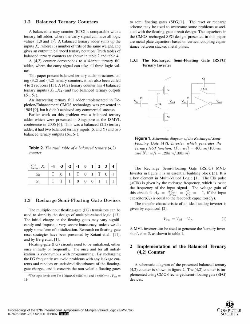
1.2 Balanced Ternary Counters
A balanced ternary counter (BTC) is comparable with aternary full adder, where the carry signal can have all logicvalues (1,0 and 1)2. A balanced ternary adder sums up theinputs Xi, where i is number of trits of the same weight, andgives an output in balanced ternary notation. Truth tables ofbalanced ternary counters are shown in table 2 and table 4.
A (4,2) counter corresponds to a 4-input ternary fulladder, where the carry signal can take all three logic val-ues.
This paper present balanced ternary adder structures, us-ing (3,2) and (4,2) ternary counters, it has also been called4 to 2 reducers [15]. A (4,2) ternary counter has 4 balancedternary inputs (X1..X4) and two balanced ternary outputs(S0, S1).
An interesting ternary full adder implemented in De-pletion/Enhancement CMOS technology was presented in1985 [9], but it didn’t achieved any commercial success.
Earlier work on this problem was a balanced ternaryadder which were presented in Singapore at the ISMVLconference in 2006 [6]. This was a balanced (2,2) ternaryadder, it had two balanced ternary inputs (X and Y) and twobalanced ternary outputs (S0, S1).
Table 2. The truth table of a balanced ternary (4,2)counter
∑4i=1 Xi -4 -3 -2 -1 0 1 2 3 4
S0 1 0 1 1 0 1 1 0 1
S1 1 1 1 0 0 0 1 1 1
1.3 Recharge Semi-Floating Gate Devices
The multiple-input floating-gate (FG) transistors can beused to simplify the design of multiple-valued logic [13].The initial charge on the floating-gates may vary signifi-cantly and impose a very severe inaccuracy, unless we doapply some form of initialization. Research on floating-gatereset strategies have been presented by Kotani et.al. [11],and by Berg et.al. [1].
Floating-gate (FG) circuits need to be initialized, eitheronce initially or frequently. The once and for all initial-ization is synonymous with programming. By rechargingthe FG frequently we avoid problems with any leakage cur-rents and random or undesired disturbance of the floating-gate charges, and it converts the non-volatile floating gates
2The logic levels are: 1 = 100mv, 0 = 500mv and 1 = 900mv , Vdd =1V
to semi floating gates (SFG)[1]. The reset or rechargescheme may be used to overcome some problems associ-ated with the floating-gate circuit design. The capacitors inthe CMOS recharged SFG design, presented in this paper,are metal plate capacitors based on vertical coupling capac-itance between stacked metal plates.
1.3.1 The Recharged Semi-Floating Gate (RSFG)Ternary Inverter
Ci
Ne
Pe
Ci
+ Clk
+ Clk
Cf
Cf
out in outV V VinV
Figure 1. Schematic diagram of the Recharged Semi-Floating Gate MVL Inverter, which generates theTernary NOT function. (Pe: w/l = 460nm/100nmand Ne: w/l = 120nm/100nm)
The Recharge Semi-Floating Gate (RSFG) MVL-Inverter in figure 1 is an essential building block [5]. It isa key element in Multi-Valued Logic [1]. The Clk pulse(+Clk) is given by the recharge frequency, which is twicethe frequency of the input signal. The voltage gain ofthis circuit is Av = ∆Vout
∆Vin= Ci
Cf= −1, if the input
capacitor(Ci) is equal to the feedback capacitor(Cf ).The transfer characteristic of an ideal analog inverter is
given by equation1 [2].
Vout = Vdd − Vin (1)
A MVL inverter can be used to generate the ’ternary inver-sion’, x = x, as shown in table 1.
2 Implementation of the Balanced Ternary(4,2) Counter
A schematic diagram of the presented balanced ternary(4,2) counter is shown in figure 2. The (4,2) counter is im-plemented using CMOS recharged semi-floating gate (SFG)devices.
Proceedings of the 37th International Symposium on Multiple-Valued Logic (ISMVL'07)0-7695-2831-7/07 $20.00 © 2007
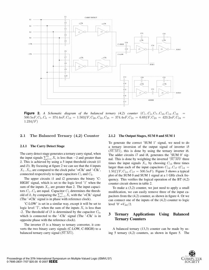
+ Clk
i 1
+ Clk
i 4
C1
C2
C3
+ Clk + Clk
C24
i 6i 5
C4
C5
C6
C7
C8
C9
C10
C23 C25
C18
C19
CARRY DETECT
SUM 1
C−LOW
C−HIGH
− Clk
+ Clk
X2
X3
X1
X4
+ Clk
i 2
+ Clk
i 3
+ Clk+ Clk
C20
C21
C22
i 7 i 8
ADDER
SUM 0
C13
C14
C15
C16
C17
SUM 1
Figure 2. A Schematic diagram of the balanced ternary (4,2) counter (C1..C4, C7..C10, C14..C19 =500.5aF,C5, C6 = 374.4aF,C13 = 1.503fF,C20, C22, C25 = 374.4aF,C21 = 6.69fF,C23 = 423.2aF,C24 =1.234fF )
2.1 The Balanced Ternary (4,2) Counter
2.1.1 The Carry Detect Stage
The carry detect stage generates a ternary carry signal, whenthe input signals
∑4i=1 Xi is less than −2 and greater than
2. This is achieved by using a 5 input threshold circuit (i1and i3). By focusing at figure 2 we can see that the 4 inputsX1..X4, are compared to the clock pulse ’+Clk’ and ’-Clk’,connected respectively to input capacitors C5 and C6.
The upper circuits i1 and i2 generates the binary ’C-HIGH’ signal, which is set to the logic level ’1’ when thesum of the inputs Xi, are greater than 2. The input capaci-tors C1..C4 are equal. Capacitor C5 determines the thresh-old of i1, by comparing the
∑4i=1 Xi with the ’+Clk’ signal
(The ’+Clk’ signal is in phase with reference clock).’C-LOW’ is set in a similar way, except it will be set to
logic level ’1’, when the sum of the inputs Xi is less than-2. The threshold of i3 is determined by the capacitor C6,which is connected to the ’-Clk’ signal (The ’-Clk’ is inopposite phase with the reference clock).
The inverter i5 is a binary to ternary converter, it con-verts the two binary carry signals (C-LOW, C-HIGH) to abalanced ternary carry signal (SUM1).
2.1.2 The Output Stages, SUM 0 and SUM 1
To generate the correct ’SUM 1’ signal, we need to doa ternary inversion of the output signal of inverter i5(SUM1), this is done by using the ternary inverter i6.The adder circuits i7 and i8, generates the ’SUM 0’ sig-nal. This is done by weighting the inverted ’SUM0’ threetimes the input signals Xi, by choosing C13 three timeslarger than each of the input capacitors C14..C17 (C13 =1.50ffF,C14..C17 = 500.5aF ). Figure 3 shows a typicalplot of the SUM 0 and SUM 1 signal at a 1 GHz clock fre-quency. This verifies the logical operation of the BT (4,2)counter circuit shown in table 2.
To make a (3,2) counter, we just need to apply a smallmodification, we can easily remove three of the input ca-pacitors from the (4,2) counter, as shown in figure 4. Or wecan connect one of the inputs of the (4,2) counter to logiclevel ’0’ =Vdd/2.
3 Ternary Applications Using BalancedTernary Counters
A balanced ternary (13,3) counter can be made by us-ing 5 ternary (4,2) counters, as shown in figure 5. The
Proceedings of the 37th International Symposium on Multiple-Valued Logic (ISMVL'07)0-7695-2831-7/07 $20.00 © 2007

Table 4. The truth table of the balanced ternary (13,3) counter∑13
i=1 Xi -13 -12 -11 -10 -9 -8 -7 -6 -5 -4 -3 -2 -1 0 1 2 3 4 5 6 7 8 9 10 11 12 13
S0 1 0 1 1 0 1 1 0 1 1 0 1 1 0 1 1 0 1 1 0 1 1 0 1 1 0 1
S1 1 1 1 0 0 0 1 1 1 1 1 1 0 0 0 1 1 1 1 1 1 0 0 0 1 1 1
S3 1 1 1 1 1 1 1 1 1 0 0 0 0 0 0 0 0 0 1 1 1 1 1 1 1 1 1
0 0.2 0.4 0.6 0.8 1 1.2 1.4 1.6 1.8
x 10−8
0
0.5
1
X1
0 0.2 0.4 0.6 0.8 1 1.2 1.4 1.6 1.8
x 10−8
0
0.5
1
X2
0 0.2 0.4 0.6 0.8 1 1.2 1.4 1.6 1.8
x 10−8
0
0.5
1
X3
0 0.2 0.4 0.6 0.8 1 1.2 1.4 1.6 1.8
x 10−8
0
0.5
1
X4
0 0.2 0.4 0.6 0.8 1 1.2 1.4 1.6 1.8
x 10−8
0
0.5
1
SU
M 0
0 0.2 0.4 0.6 0.8 1 1.2 1.4 1.6 1.8
x 10−8
0
0.5
1
SU
M 1
Figure 3. Typical outputs from the (4,2) balancedternary counter shown in figure 2
truth table of the (13,3) counter can be seen in table 4.A block diagram of the complete 4 trits balanced ternaryparallel adder using (4,2) BTC’s is shown in figure 6. Theinput vectors are: Xi = [1110], Yi = [1111], Xi = [0010],which correspond with 15-32+3=-14 in decimal notation.The SUM=[1111]3=−1410. Figure 7 verifies the opera-tion of the circuit. It is also possible to build a Wallacetree structure by using balanced ternary counters. A Wal-lace tree adder sums up all trits of the same weights in amerged tree, and do not add the partial products in pairs asa balanced ternary parallel adder does. Figure 8 shows abalanced ternary Wallace tree adder.
3.1 Advantages Using Balanced TernaryCounters
Mostly all of the binary adder structures are directly con-vert able to balanced ternary adder structures. This meansyou can be able to replace the binary full adders with ternary
+ Clk+ Clk
i 3
C−HIGH
C−LOWCARRY DETECT
i 4
C1
C2
C6
C5
C4
+ Clk + Clk
i 2i 1
C9
C8
C7
C3
C10
C11
C12
X1
X2
+ Clk
− Clk
SUM 1
SUM 0
X3
_____SUM 1
Figure 4. A block diagram of a balanced ternary(3,2) counter
balanced counters, and still have the same functionality.However there is an advantage using balanced ternary nota-tion, you do not have to worry about the sign bit, and youneed less trits to make the same resolution.
Figure 6 shows a 4-trits parallel balanced ternary adder(BTA), which is comparable with a 6-bit ripple carry adderif we consider the resolution. To build a 6-bit ripple carryadder we need 6 full-adders (FA), compared to 4 balancedternary counters (BTC). A typical binary FA uses 28 tran-sistors, the presented BTC uses 32 transistors. This givesus, a 4-trits balanced ternary adder needs 128 transistors,compared to a binary 6-bits adder which needs 168 transis-tors. See table 3. A 11-bit FA uses 308 transistors this iscomparable with a 7-trits BTA which uses 224 transistors.Figure 9 shows this graphically, even for low resolutions itis better to use a parallel BTA compared to a binary ripplecarry adder. It is also possible to make carry-save adderstructures using balanced ternary counters. This makes iteasy to implement balanced ternary counters in fast addi-tion structures, based on binary logical adder theory.
A floating gate structure will generally generate a largerchip area compared to a conventional design because of thecapacitors. By using very small metal-capacitors and usingstacking, we are able to minimize the chip area. The used90nm CMOS process from STMicroelectronics, has 7 metallayers.
Proceedings of the 37th International Symposium on Multiple-Valued Logic (ISMVL'07)0-7695-2831-7/07 $20.00 © 2007

Table 3. Comparison between a binary ripple carryadder and a parallel balanced ternary adder
Bits Resolution Transistors Trits Resolution Transistors
1 2 28 1 3 32
2 4 56 2 9 64
3 8 84 3 27 96
4 16 112 4 81 128
5 32 140 5 243 160
6 64 168 6 729 192
7 128 196 7 2187 224
8 256 224 8 6561 256
9 512 252 9 19683 288
10 1024 280 10 59049 320
11 2048 308 11 177147 352
12 4096 336 12 531441 384
13 8192 364 13 1594323 416
14 16384 392 14 4782969 448
15 32768 420 15 14348907 480
16 65536 448 16 43046721 512
4 Conclusions
In this paper, a balanced ternary adder structures usingbalanced ternary counters has been presented. It has thebenefitcal properties as following:
1. There is no reason to worry about the sign bit, sincethe structures use balanced ternary notation.
2. The resolution compared to numbers of transistorgives a higher resolution than with a typical binary solution,this is shown graphically in figure 9.
It is possible to build fast addition structures, using thetheory from the binary world. The simulation results showsthat the circuits may be able to operate at clock frequencyof 1 GHz. The circuits can be made using a conventionalCMOS process. We are using a 90nm general purpose bulkCMOS process from STMicroelectronics with 7 metal lay-ers.
References
[1] Y. Berg, S. Aunet, O. Mirmotahari, and M. Høvin. NovelRecharge Semi-Floating-Gate CMOS Logic For Multiple-Valued Systems. Proceedings of the 2003 IEEE Inter-national Symposium on Circuits And Systems in Bangkok,2003.
(4,2)
BTC
(4,2)
BTC
(4,2)
BTC
(4,2)
BTC
(4,2)
BTC
S2 S0
X10X11X12X13 X1X2X3X4X5X6X7X8X9
S1
Figure 5. A balanced ternary (13,3) counter
BTC(4,2)
BTC(4,2)
BTC(4,2)
BTC(4,2)
S1S2 S1 S0S3 S2S3S4
Z3 Y3 X3 Z2 Y2 X2 Z1 Y1 X1 Z0 Y0 X0
S4 S3 S2 S1 S0
C0
Figure 6. A Block schematic diagram of a 4 trits par-allel balanced ternary adder
[2] Y. Berg, T. S. Lande, Ø. Næss, and H. Gundersen. Ultra-Low-Voltage Floating Gate Transconductance Amplifiers.IEEE Trans. Circuits and Systems-II: Analog and DigitalSignal Processing,vol.48,no.1, Jan. 2001.
[3] K. Diawuo and H. T. Mouftah. A Three-Valued CMOSArithmetic Logic Unit Chip. Proceedings of the 17th IEEEInternational Symposium on Multiple-Valued Logic, pages215–220, 1987.
[4] M. Glusker, D. M. Hogan, and P. Vass. The Ternary Cal-cualating Machine of Thomas Fowler. IEEE Annals of theHistory of Computing, pages 4–22, 2005.
[5] H. Gundersen and Y. Berg. MAX and MIN Functions Us-ing Multiple-Valued Recharged Semi-Floating Gate Circuits.Proceedings of the 2004 IEEE International Symposium onCircuits And Systems in Vancouver, 2004.
[6] H. Gundersen and Y. Berg. A Novel Balanced TernaryAdder Using CMOS Recharged Semi-Floating Gate De-vices. Proceedings of the 36th IEEE International Sympo-sium on Multiple-Valued Logic in Singapore, page 18, 2006.
[7] B. Hayes. Third Base. American Scientist, Volume 89, Num-ber 6, pages 490–494, Nov-Dec 2001.
[8] A. Herrfeld and S. Hentsche. Ternary Multiplications Using4-Input Adder Cells and Carry Look-Ahead. Proceedings of
Proceedings of the 37th International Symposium on Multiple-Valued Logic (ISMVL'07)0-7695-2831-7/07 $20.00 © 2007

0 1 2 3 4 5 6
x 10−9
0
0.5
1
S0
0 1 2 3 4 5 6
x 10−9
0
0.5
1
S1
0 1 2 3 4 5 6
x 10−9
0
0.5
1
S2
0 1 2 3 4 5 6
x 10−9
0
0.5
1
S3
0 1 2 3 4 5 6
x 10−9
0
0.5
1
S4
Figure 7. Typical output signals (S0..S4) of the 4 tritsparallel adder shown in figure 6. SUM = [01111].The clock frequency is 1 GHz
the 29th IEEE International Symposium on Multiple-ValuedLogic, 1999.
[9] A. Heung and H. T. Mouftah. Depletion/EnhancementCMOS For a Low Power Family of Three-Valued Logic Cir-cuits. IEEE Journal of Solid-State Circuits, VOL. sc-20, NO.2, pages 609–616, April 1985.
[10] D. Knuth. The Art of Computer Programming, Second edi-tion. Addison-Wesley Publishing Company, 1981.
[11] K. Kotani, T. Shibata, M. Imai, and T. Ohmi. ClockedNeuron-MOS Logic Circuits Employing Auto Threhold Ad-justment. IEEE International Solid-State Circuits Confer-ence(ISSCC), pages 320–321,388, 1995.
[12] T. N. Rajashekhara and I. E. Chen. A Fast Adder DesignUsing Signed-Digit Numbers and Ternary Logic. Proceed-ings of the 1990 IEEE International Symposium on Multiple-Valued Logic, pages 187–194, 1990.
[13] T. Shibata and T. Ohmi. A Functional MOS Transistor Fea-turing Gate-Level Weighted Sum and Threshold Operations.IEEE Transactions on Electron devices, 39(6):1444–1455,1992.
[14] S. Stakhov. Brousentsov’s Ternary Principle, Bergman’Number System and Ternary Mirror-symmetrical Arith-metic. The Computer Journal, Vol. 45, No.2, pages 221–236,2002.
[15] Z. G. Vranesic and V. C. Hamacher. Threshold Logic in FastTernary Multipliers. Proceedings of the 1975 IEEE Interna-tional Symposium on Multiple-Valued Logic, pages 373–387,1975.
(3,2)
BTC
X6 X5 X4
(3,2)
BTC
(3,2)
BTC
(3,2)
BTC
(3,2)
BTC
(3,2)
BTC
X9 X8 X7
(3,2)
BTC
X3 X2 X1
Figure 8. A balanced ternary Wallace tree adder, us-ing (3,2) ternary counters
0 100 200 300 400 50010
0
102
104
106
108
1010
Number of transistors
Res
olut
ion
Ripple carry adderParallel balanced ternary adder
Figure 9. Resolution compared to number of transis-tors of the presented parallel balanced ternary adderand a typical binary ripple carry adder
Proceedings of the 37th International Symposium on Multiple-Valued Logic (ISMVL'07)0-7695-2831-7/07 $20.00 © 2007

7.7 PAPER VII: A Balanced Ternary MultiplicationCircuit Using Recharged Semi-Floating Gate Devices
Henning Gundersen and Yngvar BergDepartment of informatics, University of Oslo
Proceedings of 24th IEEE Norchip Coference,NORCHIP, Linkoping Sweden, Nov. 20-21, 2006,
ISBN 0-4244-0772-9, Page 205-208
93

94

A Balanced Ternary Multiplication Circuit UsingRecharged Semi-Floating Gate Devices
Henning Gundersen and Yngvar BergDepartment of Informatics, Microelectronic Systems Group, University of Oslo
Blindern, NO-0316, Oslo, NorwayEmail: [email protected]
Abstract— This paper presents a multiplier circuit using Bal-anced Ternary (BT) Notation. The multiplier can multiply bothnegative and positive numbers, which is one of the advantageable properties of the balanced ternary numbering systems.By using balanced ternary notation, it is possible to takeadvantage of carry free multiplication, which is exploited indesigning a fast multiplier circuit. The circuit is implementedwith Recharged Semi-Floating Gate (RSFG) devices. The circuitoperates at 1 GHz clock frequency at a supply voltage of only1.0 Volt. The circuit is simulated by using Cadence R©AnalogDesign Environment, with CMOS090 process parameters, a 90nmGeneral Purpose Bulk CMOS Process from STMicroelectronicswith 7 metal layers.
I. INTRODUCTION
Nowadays almost all multiplication done with computersare binary multiplications. Multiplying two positive numbersin a binary numbering system is trivial, but if we wantto deal with negative numbers, it is not that trivial. Whendoing multiplication with negative numbers you usually needa sign bit and you have to use the 2’ complement. Thatis why I suggest using balanced ternary numbering systeminstead, to make a solution to the sign problem. The so-called’Brousentsov’s Ternary Principle’ of computer design was firstrealized in the Setun computer [1] and this computer used a’ternary-symmetrical number system’, which is another namefor the balanced ternary notation. There has also been someother attempts to implement arithmetic applications whichuse the ternary numbering system, but they lack commercialsuccess [2] [3].
A. The Balanced Ternary Number Systems
’Ternary numbering systems is the most efficient of allinteger bases’ as Brian Hayes claims in his article Third Base[4]. Balanced ternary notation is a number system which usebase 3 representation. Balanced ternary notation is ’Perhapsthe prettiest number system of all’ as Donald Knuth saidin his book, The Art of Computer Programming [5]. Inthe balanced ternary the digits are also powers of 3, as inordinary ternary numbers, but they are ’balanced’ since theyare symmetrical about zero. A given example of a balancedternary number is the decimal number 23. It is written inbalanced ternary notation as: 1011. This numeral is interpretedas: 1x33 + 0x32 − 1x31 − 1x30, or 27 + 0 - 3 - 1, in decimalnotation. The balanced ternary number system has also someadvantage able properties:
a) ’Ternary inversion’ [1] is easy, change 1 with 1, and vicaversa. If we use the example -23, the result will be 1011 inbalanced ternary notation.b) The sign of a number is given by its most significantnonzero ’trit1’c) The operation of rounding to the nearest integer is identicalto truncation.d) Addition and subtraction are essentially the same operation:just apply the rules of ’ternary inversion’ to one of thenumbers, and afterwards doing an adding operation.
B. Balanced Ternary Arithmetic
In 1840 Thomas Fowler, a self-taught English mathemati-cian invented a ternary mechanical calculating machine whichused balanced ternary notation. All details on the calulatingmachine was lost, until recently. A research project whichbegan in 1997 have managed to get all the information whichis needed to create a historical replica [6]. Fowler used theterms -, 0 and + for a negative, a zero and a positive number.We will use the terms 1, 0 and 1. Arithmetic in balancedternary notation is almost the same as any other alternativebase, except it can handle negative and positive numbers.This means that it can be both negative and positive carryto adjacent digits.
1 decimal 1
+ 1 decimal 1
= 1 1 decimal 2
Examples of positive carry in balanced teranary addition.
1 1 decimal 2
+ 1 1 decimal 2
= 1 1 decimal 4
Examples of negative carry in balanced teranary addition.
1One trit has 3 values, the values are ( 1, 0, 1), it is analogous to bit in thebinary world (0 , 1).

Multiplication in balanced ternary notation is done in thesimilar manner as with decimal multiplication. The truth tableof a balanced ternary multipication is shown in table I.Multiplication is done one digit a time. The choice of each
TABLE I
THE TRUTH TABLE OF A BALANCED TERNARY MULTIPLICATION CIRCUIT
-1 0 1
-1 1 0 -1
0 0 0 0
1 -1 0 1
digit is simple, if the digit is 1 then invert, if it is 0 then setit to zero, if it is 1 then multiply by one. For example themultipication og 2 x 8 = 16 (decimal) is 1 1 x 1 0 1 = 1 1 1 1in balanced ternary notation. The calculation is done as shownin the table II. In the first row the multiplicand is inverted byusing ’ternary inversion’. In the second row, shift one timeleft, then multiply with ’0’. In the third row, shift left, thenmultiply with ’1’. Then the three numbers are added togetherusing a balanced ternary adder.
TABLE II
AN EXAMPLE OF AN BALANCED TERNARY MULTIPLICATION.
1 1 Invert multiplicand
0 0 0 times multiplicand
1 1 1 times multiplicand
1 1 1 1 decimal 16
C. Recharge Semi-Floating Gate Devices
The multiple-input floating-gate (FG) transistors can beused to simplify the design of multiple-valued logic [7]. Theinitial charge on the floating-gates may vary significantly andtherefore impose a very severe inaccuracy, unless we do applysome form of initialization. Research on floating-gate resetstrategies have been presented by Kotani et.al. [8], and byBerg et.al. [9].
Floating-gate (FG) circuits need to be initialized, eitheronce initially or frequently. The once and for all initializationis synonymous with programming. By recharging the FGfrequently we avoid problems with any leakage currents andrandom or undesired disturbance of the floating-gate charges,and we convert the non-volatile floating gates to Semi FloatingGates (SFG)[9]. The reset or recharged scheme may be usedto overcome some problems associated with the floating-gatecircuit design.
All of the capacitors in the CMOS RSFG design presentedin this paper are metal plate capacitors, based on verticalcoupling capacitance between stacked metal plates.
D. The Recharged Semi-Floating Gate (RSFG) Ternary In-verter
Ci
Ne
Pe
Ci
+ Clk
+ Clk
Cf
Cf
out in outV V VinV
Fig. 1. Schematic diagram of the Recharged Semi-Floating Gate MVLInverter, which generates the Ternary NOT function. The transistor sizes arePe (w = 460nm and l = 100nm) and Ne (w = 120nm and l = 100nm)
The Recharge Semi-Floating Gate (RSFG) MVL-Inverterin figure 1 is an important application [10]. This is a keyelement in Multi-Valued Logic [9]. A MVL inverter, alsocalled an analog inverter, is an inverter with a negativefeedback mechanism, Cf . The voltage gain of this circuit isAv = ∆Vout
∆Vin= −1. The transfer characteristic of the analog
inverter is given by equation1 [11].
Vout = Vdd − Vin (1)
A MVL inverter can be used to generate the ’ternary inver-sion’. The truth table of the rule of ’ternary inversion’ is shownin table III.
TABLE III
THE TRUTH TABLE OF THE RULE OF ’TERNARY INVERSION’
Vin Vout
1 1
0 0
1 1
II. IMPLEMENTATION OF THE BALANCED TERNARY
MULTIPLICATION CIRCUIT USING RECHARGED
SEMI-FLOATING GATE DEVICES
A block scheme of the proposed BT-multiplication circuitis shown in figure 2. The input data is set into a shift register,and here the data is shifted and leading zeros are inserted inthe input vectors X, Y and Z. From the shift register the 4-tritsdata are sent to each of the vectors X,Y and Z. X Y and Z arethe input signals to the 4-trits BT-Adder. The outputs from theBT-Multiplication (BTM) circuit are S0, S1, S2, S3 and S4.
A. A Balanced 3,2 Ternary Counter
A balanced 3,2 ternary counter, can also be seen as a 3-input ternary full adder, where the carry signal can take allthree logic values (1, 0, 1). The balanced 3,2 ternary counter

1_
1_
S4 S3 S2 S1 S0
Y
X 0 0 1
1
0 0 00
0 0
DATA
4 TRITS BALANCED TERNARY ADDER
SHIFT REGISTER
Z
Y2Z0Z2 Y3 Y1 Y0 X2 X1 X0X3Z1Z3
Fig. 2. The Block Scheme of the multiplication circuit
TABLE IV
THE TRUTH TABLE OF A BALANCED 3,2 TERNARY COUNTER
∑(X + Y + Z) -3 -2 -1 0 1 2 3
S0 0 1 1 0 1 1 0
S1 1 1 0 0 0 1 1
(BTC) is shown in figure 3, the truth table of the (3,2) BTCis shown in table IV.
The Balanced 3,2 Ternary Counter takes three ternary inputsX, Y and Z, and generates two outputs, S0 and S1. Thiscounter counts from -3 to +3. The full truth table is shownin table V. The simulation results of the (3,2) BTC is shownin figure 4, when the logic input signal X is set to 0.
The Carry detect stage will detect when two or three of theinputs are high or low. This will then generate the binary high-(C-HIGH) or binary low- (C-LOW) carry signal. The C-HIGHand C-LOW signal are combined to a ternary signal SUM1.By adding the SUM1 with the input signals X, Y and Z, byusing a 4-input ternary inverter (i1), we get the correct SUM0 signal. A similar balanced ternary adder were presented inSingapore at the ISMVL2006 conference [12]. It had a twobalanced ternary inputs (X and Y) and two outputs, S0 andS1, but the main idea of operation is almost the same.
B. The Balanced Ternary Multiplication Circuit
A balanced ternary counter is a key element in a multipli-cation application. To make a 4-trits BT-Adder (figure 6) weneed to use 8 balanced 3,2 ternary counters (BTC) which isshown in figure 3. The output stage (4-trits BTA) of the 4-trits balanced ternary multiplication (BTM) circuit shown infigure 2, consists of 8 BTC’s. The SUM output signals is S0,S1, S2, S3 and S4. The input vectors X, Y and Z to the 4-trits BTA (the output stage) will either be inverted, be zeroor be unchanged. If we take the example 2 x 8 (decimal) 11
+ Clk+ Clk
i 3
C−HIGH
C−LOWCARRY DETECT
i 4
C1
C2
C6
C5
C4
+ Clk + Clk
i 2i 1
C9
C8
C7
C3
C10
C11
C12
X
Y
Z
S0
S1
_____SUM 1
Fig. 3. A Block Schematic diagram of the Balanced 3,2 Ternary Counter
0 0.2 0.4 0.6 0.8 1 1.2 1.4 1.6 1.8 2
x 10−8
0
0.5
1
X
0 0.2 0.4 0.6 0.8 1 1.2 1.4 1.6 1.8 2
x 10−8
0
0.5
1
Y
0 0.2 0.4 0.6 0.8 1 1.2 1.4 1.6 1.8 2
x 10−8
0
0.5
1
Z
0 0.2 0.4 0.6 0.8 1 1.2 1.4 1.6 1.8 2
x 10−8
0
0.5
1
SU
M 0
0 0.2 0.4 0.6 0.8 1 1.2 1.4 1.6 1.8 2
x 10−8
0
0.5
1
SU
M 1
Fig. 4. Simulation results for the Balanced 3,2 Ternary Counter shown infigure 3.
x 101 (balanced ternary) shown in table II. The first productis the inverted, of the multiplicand which generates the 4-tritsX vector X=[1 1 0 0]. The second product should be set to0, which gives the Y vector Y=[0 0 0 0]. The third productis first shifted 2 times left and then 1 times multiplicand thisgives the Z vector Z=[0 0 1 1]. Figure 5 shows the input tothe output stage. X is inverted using a ternary inversion, Y isset to ’0’ and Z propagates to the input of the 4-trits BTA. Tomake this possible, a multiplexer-switch must be set on theinput to the BTA circuit.
Figure 6 shows the propagation of the trits in the outputstage. Since the BTC are 3,2 counter some of the inputs ofthe BTCs has to be set to ’zero’ as shown in the figure 6. Thesignal S0 has less delay. The signal S4 has the longest pathand this will determined the maximum operation frequency ofthis circuit.
Figure 7 shows the simulated output plots of the BT-Multiplication circuit. The figure shows the output vector

TABLE V
THE FULL TRUTH TABLE OF THE BALANCED 3,2 TERNARY COUNTER
X 1 1 1 1 1 1 1 1 1 0 0 0 0 0 0 0 0 0 1 1 1 1 1 1 1 1 1
Y 1 1 1 0 0 0 1 1 1 1 1 1 0 0 0 1 1 1 1 1 1 0 0 0 1 1 1
Z 1 0 1 1 0 1 1 0 1 1 0 1 1 0 1 1 0 1 1 0 1 1 0 1 1 0 1
SUM 10 11 01 11 01 00 01 00 01 11 01 00 01 00 01 00 01 11 01 00 01 00 01 11 01 11 10
X
1__
1__
1__
Y
Z
S1
S0
0 0 0
001
0
X__
100 100
S2
S3
S4
4 TRITS BTA
Fig. 5. The input vectors to the 4-trits Balanced Ternary Adder
SUM=[S3 S2 S1 S0] = [1 1 1 1], the result of the simulationcorrespond with the total sum of the multiplication done intable II. S4 is ’zero’ and is not shown.
_1
_1
_1
_1
_1
_1
_1
_1
(3,2)
BTC
(3,2)
BTC
(3,2)
BTC
(3,2)
BTC
(3,2)
BTC
(3,2)
BTC(3,2)
BTC
(3,2)
BTC
’ 0 ’
’ 0 ’
S4
S4 S3 S2 S1 S0
S2 S1
11 00000 0
110 0
0
0
0 0
0 0
110
0 1
Z2 Y2 X2
S2S3
Z1 Y1 X1
S1S2
Z0 Y0 X0
S1 S0
S3 S2
S3S4
Z3 Y3 X3
S3S4
Fig. 6. A block diagram of the 4-trits Balanced Ternary Adder showing thepropagation of the trits
III. CONCLUSIONS
In this paper a 4-trits Balanced Ternary Multiplication(BTM) circuit has been presented. It has some advantage ableproperties, it handles multiplication with both negative andpositive numbers, which is one of the benefits using balancedternary notation. This application shows that it is possibleto build a fast multiplier circuit if we use balanced ternarynotation, and by using a conventional CMOS Process. Theproposed BTM operates at a clock frequency at 1 GHz at aload of 10fF .
1 1.2 1.4 1.6 1.8 2 2.2 2.4 2.6 2.8 3
x 10−9
0
0.5
1
S0
1 1.2 1.4 1.6 1.8 2 2.2 2.4 2.6 2.8 3
x 10−9
0
0.5
1
S1
1 1.2 1.4 1.6 1.8 2 2.2 2.4 2.6 2.8 3
x 10−9
0
0.5
1
S2
1 1.2 1.4 1.6 1.8 2 2.2 2.4 2.6 2.8 3
x 10−9
0
0.5
1
S3
Fig. 7. A plot of the outputs from the Balanced Ternary Multiplication circuit
REFERENCES
[1] S. Stakhov, “Brousentsov’s Ternary Principle, Bergman’ Number Systemand Ternary Mirror-symmetrical Arithmetic,” The Computer Journal,Vol. 45, No.2, pp. 221–236, 2002.
[2] A. Herrfeld and S. Hentsche, “Ternary Multiplications Using 4-InputAdder Cells and Carry Look-Ahead,” Proceedings of the 29th IEEEInternational Symposium on Multiple-Valued Logic, 1999.
[3] K. Diawuo and H. T. Mouftah, “A Three-Valued CMOS ArithmeticLogic Unit Chip,” Proceedings of the 17th IEEE International Sympo-sium on Multiple-Valued Logic, pp. 215–220, 1987.
[4] B. Hayes, “Third Base,” American Scientist, Volume 89, Number 6, pp.490–494, Nov-Dec 2001.
[5] D. Knuth, The Art of Computer Programming, Second edition. Addison-Wesley Publishing Company, 1981.
[6] M. Glusker, D. M. Hogan, and P. Vass, “The Ternary CalcualatingMachine of Thomas Fowler,” IEEE Annals of the History of Computing,pp. 4–22, 2005.
[7] T. Shibata and T. Ohmi, “A Functional MOS Transistor Featuring Gate-Level Weighted Sum and Threshold Operations,” IEEE Transactions onElectron devices, vol. 39(6), pp. 1444–1455, 1992.
[8] K. Kotani, T. Shibata, M. Imai, and T. Ohmi, “Clocked Neuron-MOS Logic Circuits Employing Auto Threhold Adjustment,” IEEEInternational Solid-State Circuits Conference(ISSCC), pp. 320–321,388,1995.
[9] Y. Berg, S. Aunet, O. Mirmotahari, and M. Høvin, “Novel RechargeSemi-Floating-Gate CMOS Logic For Multiple-Valued Systems,” Pro-ceedings of the 2003 IEEE International Symposium on Circuits AndSystems in Bangkok, 2003.
[10] H. Gundersen and Y. Berg, “MAX and MIN Functions Using Multiple-Valued Recharged Semi-Floating Gate Circuits,” Proceedings of the2004 IEEE International Symposium on Circuits And Systems in Van-couver, 2004.
[11] Y. Berg, T. S. Lande, Ø. Næss, and H. Gundersen, “Ultra-Low-VoltageFloating Gate Transconductance Amplifiers,” IEEE Trans. Circuits andSystems-II: Analog and Digital Signal Processing,vol.48,no.1, Jan. 2001.
[12] H. Gundersen and Y. Berg, “A Novel Balanced Ternary Adder UsingCMOS Recharged Semi-Floating Gate Devices,” Proceedings of the 36thIEEE International Symposium on Multiple-Valued Logic in Singapore,p. 18, 2006.

Appendix A
ADDITIONAL INFORMATION
99

100

A.1 Measurement Information
A prototype chip was fabricated by STMicroelectronics using a 90nm CMOS process. Itcontained some simple RSFG structures, a Ternary-NOT circuit, an AUTO-ZERO circuit),a MAX circuit, a More-Less and Equality circuit, and a simple balanced ternary adder.The measurement equipment set-up is shown in Figure A.1 and A.2.
Figure A.1: Set-up of the measuring instruments used
A.1.1 Instruments
The instrument where controlled using the GPIB interface connected to a Linux PC, withMATLAB 7.5.0.338 installed. All scripts where written in MATLAB. The HP/AGILENT33250 where used as the reference clock. All input signals to the chip where DC-signalsgenerated by KEITHLEY 213. The output was measured by using 10:1 probes connectedto TEKTRONIX TDS 3052. HP/AGILENT E3631A served as the power supply to thechip. The multimeter HP/AGILENT 34401A monitored the input signals.A list of the instruments I used, is given in Table A.1.
Table A.1: Measurement instruments
HP/AGILIENT E3631A Power Supply
HP/AGILIENT 33250A Function Arbitrary Waweform Generator
HP/AGILIENT 34401A Multimeter
KEITHLEY 213 Quad Voltage Source
TEKTRONIX TDS 3052 Digital Oscilloscope
TEKTRONIX TEK P6139A Probes (500MHZ, 8.0pF, 10MΩ, 10X)
101

(a) The set-up (b) A closer look
Figure A.2: A typical set-up of the measurement jig
A.1.2 The Prototype Printed Circuit Board
The prototype printed circuit board (PCB) was made by using FreePCB, after readinga short turtorial on PCB design [41]. FreePCB is a free, open-source PCB editor forMicrosoft Windows, released under the GNU General Public License [73]. A picture ofthe PCB with the prototype chip is shown in figure A.4 and the layout of the PCB isshown in figure A.3.
102

Figure A.3: Layout of the PCB
Figure A.4: Picture of the PCB with the mounted prototype chip
103

104

Appendix B
ABBREVIATIONS
Below are some of the abbreviations used in this thesis.
ADC Analog-to-Digital ConverterALU In computing, an arithmetic logic unit (ALU) is a digital circuit
that performs arithmetic and logical operationsBT Balanced TernaryCMOS Complementary Metal Oxide SemiconductorCPU Central Processing UnitDLC Down Literal CircuitFG Floating GateFGUVMOS Floating Gate UltraViolet light Metal Oxide SemiconductorMAX The MAXimum function is analogues with the
OR function in binary logicMIN The MINimum function is analogues with the
AND function in binary logicMOSFET Metal Oxide Semiconductor Field Effect TransistorMVL Multiple-Valued LogicNMOS N-channel MOSFETPCB Printed Circuit BoardPG Pass Gate transistorPMOS P-channel MOSFETRSFG Recharged Semi-Floating GateSRAM Static Read Only MemorySUS-LOC SUpplementary Symmetrical LOgic Circuit
105

106

List of Figures
2.1 Floating gate structures . . . . . . . . . . . . . . . . . . . . . . . . . . . . . 6
2.2 A n-input NMOS FG transistor . . . . . . . . . . . . . . . . . . . . . . . . . 7
2.3 Capacitive division model, (a) Schematic of the transistor model with theparasictic capacitors included. (b) Equivalent capacitive divider model . . . 8
2.4 Gate structures used in FG technology . . . . . . . . . . . . . . . . . . . . . 9
2.5 A typical recharged semi-floating gate binary inverter. . . . . . . . . . . . . 11
2.6 A simple clock generator. . . . . . . . . . . . . . . . . . . . . . . . . . . . . 13
2.7 Characteristics of the simple clock generator implemented in 90nm CMOStechnology, the reference clock is 1 GHz . . . . . . . . . . . . . . . . . . . . 14
2.8 Typical auto-zero elements . . . . . . . . . . . . . . . . . . . . . . . . . . . . 15
2.9 Clocked CMOS gate, used to remove the recharge clock, to create a non-recharged signal . . . . . . . . . . . . . . . . . . . . . . . . . . . . . . . . . . 16
2.10 Measured output characteristics of the auto-zero element in figure 2.8(a)with input signals -1 and +1 . . . . . . . . . . . . . . . . . . . . . . . . . . 17
2.11 Measured output characteristics of the auto-zero element in figure 2.8(a)with input signal +0 . . . . . . . . . . . . . . . . . . . . . . . . . . . . . . . 17
2.12 Measured DC response of the RSFG binary inverter . . . . . . . . . . . . . 18
2.13 Measured output characteristics of the binary RSFG inverter with inputsignals −1 and +1 . . . . . . . . . . . . . . . . . . . . . . . . . . . . . . . . 18
3.1 A typical RSFG MVL Inverter . . . . . . . . . . . . . . . . . . . . . . . . . 23
3.2 A down literal circuit . . . . . . . . . . . . . . . . . . . . . . . . . . . . . . . 25
3.3 A RSFG MAX circuit . . . . . . . . . . . . . . . . . . . . . . . . . . . . . . 25
3.4 A RSFG MIN circuit . . . . . . . . . . . . . . . . . . . . . . . . . . . . . . . 26
3.5 Measured DC response of a RSFG MVL inverter in 90nm CMOS technology 26
3.6 Measured output charcteristics of the RSFG MAX-circuit . . . . . . . . . . 27
3.7 Measured output characteristics of the MAX circuit with input signals (−1,−1)and (−1, +0) . . . . . . . . . . . . . . . . . . . . . . . . . . . . . . . . . . . 28
3.8 Measured output characteristics of the MAX circuit with input signal (−1,+1) 28
3.9 Measured output characteristics of a RSFG MVL inverter in 90nm CMOStechnology with input signal +1 and −1 . . . . . . . . . . . . . . . . . . . . 29
3.10 Measured output characteristics of a RSFG MVL inverter in 90nm CMOStechnology with input signal +0 . . . . . . . . . . . . . . . . . . . . . . . . . 29
4.1 A more, less or equal circuit . . . . . . . . . . . . . . . . . . . . . . . . . . . 33
4.2 A typical output plot of the more, less or equality circuit . . . . . . . . . . . 34
107

4.3 Measured output characteristics of the RSFG MLE circuit in 90nm Technology 354.4 A Ternary Switching Element . . . . . . . . . . . . . . . . . . . . . . . . . . 364.5 Vout vs Vin of the ternary switching element, the supply voltage; Vdd = 2V 374.6 Measured output characteristics of the RSFG MLE circuit in 90nm CMOS
Technology with input signals (−1,−1) and (−1,+1) . . . . . . . . . . . . . 384.7 Measured output characteristics of the RSFG MLE circuit in 90nm CMOS
Technology with input signal (+1,−1) . . . . . . . . . . . . . . . . . . . . . 38
5.1 A RSFG balanced ternary adder . . . . . . . . . . . . . . . . . . . . . . . . . 405.2 A balanced ternary (4,2) counter . . . . . . . . . . . . . . . . . . . . . . . . 435.3 An example of a 4 trits parallel balanced ternary adder using (4,2) counters 445.4 An example of a balanced ternary multiplication . . . . . . . . . . . . . . . . 455.5 Measured output characteristics of the BTA circuit, with input signal (−1,
−1) . . . . . . . . . . . . . . . . . . . . . . . . . . . . . . . . . . . . . . . . 455.6 Measured output characteristics of the BTA circuit, with input signal (+0,+0) 465.7 Measured output characteristics of the BTA circuit, with input signal (+1,+1) 46
A.1 Set-up of the measuring instruments used . . . . . . . . . . . . . . . . . . . 101A.2 A typical set-up of the measurement jig . . . . . . . . . . . . . . . . . . . . 102A.3 Layout of the PCB . . . . . . . . . . . . . . . . . . . . . . . . . . . . . . . . 103A.4 Picture of the PCB with the mounted prototype chip . . . . . . . . . . . . . 103
108
Bibliography
[1] M. Aline, T. Saidi, and E. D. Olson. Design and Characterization of a Low PowerTernary DSP. International Signal Processing Conference, 2003.
[2] R. Appleyard. The Direct Measurement of the Napierian Base. Proc. Phys. Soc.London, 26:178–182, 1913.
[3] Snorre Aunet. Real-time Reconfigurable Devices Implemented in UV-light Pro-grammable Floating-Gate CMOS. Dr. Scient. thesis, Department of computer andinformation science, Norwegian University of Science and Technology (NTNU), 2002.ISBN 82-471-5447-1.
[4] V. Beiu, J. M. Quintana, and M. J. Avedillo. VLSI Implementation of ThresholdLogic-A Comprehensive Survey. IEEE Transactions on Neural Networks, 14(5):1217–1243, 2003.
[5] Y. Berg, S. Aunet, O. Mirmotahari, and M. Høvin. Novel Recharged Semi-Floating-Gate CMOS Logic for Multiple-Valued Systems. Proceedings of the 2003 IEEE In-ternational Symposium on Circuits and Systems, Bangkok, 5:193–196, 2003.
[6] Y. Berg, S. Aunet, Ø. Næss, J. G.Lomsdalen, J. Bush, and M. Høvin. Binary In-put Multiple-Valued Recharge CMOS Full-Adders. Euopean Conference on CircuitTheory and Design, Poland, pages 365–368, 2003.
[7] Y. Berg, S. Aunet, Ø. Næss, and O. Mirmotahari. Basic Multiple-Valued Functionsusing Regharge CMOS Logic. Proceedings of the 34th International Symposium onMultiple-Valued Logic, pages 346–351, 2004.
[8] Y. Berg, S. Aunet, Ø. Næss, O. Mirmotahari, and M. Høvin. Binary to Multiple-Valued Recharge Converter for Multiple-Valued CMOS logic. Euopean Conferenceon Circuit Theory and Design, Poland, pages 349–352, 2003.
[9] Y. Berg, R. Jensen, J. G. Lomsadalen, H. Gundersen, and S. Aunet. Fault TolerantCMOS Logic using Ternary Gates. Proceedings IEEE 37th International Symposiumon Multiple-Valued Logic, 2007.
[10] Y. Berg and T. S. Lande. Programmable Floating-Gate MOS Logic for Low-PowerOperation. IEEE International Symposium on Circuits and Systems, 3:1792–1795,1997.
109
[11] Y. Berg, T. S. Lande, O. Næss, and H. Gundersen. Ultra Low-Voltage FloatingGate Transconductance Amplifiers. IEEE Trans. Circuits and Systems-II: Analogand Digital Signal Processing, 48(1), Jan. 2001.
[12] Y. Berg, O. Mirmotahari, P. A. Norseng, and S. Aunet. Ultra Low Voltage CMOSGates. Proceedings of the 13th International Conference on Electronics, Circuits andSystems, pages 818–821, 2006.
[13] Y. Berg, O. Næss, M. Høvin, and H. Gundersen. Ultra Low-voltage Floating-gate(FGUVMOS) Amplifiers. Analog Integrated Circuits and Signal Processing, 26:63–73,2001.
[14] N. P. Brusentov. The Computer ’Setun’ of Moscow University. Material of theScientific-technical Conference: New Developments in Computational Mathematicsand Computing Techniques, pages 226–234, 1960.
[15] J. R. Burns and R. A. Powlus. Threshold Circuit Utilizing Fields Effect Transistors.U.S. Patent 3 260 863, July 12, 1966.
[16] R. S. Chau. Intel’s Breakthrough in High-K Gate Dielectric Drives Moore’s Law Wellinto the Future. Technology@Intel Magazine, pages 1–7, January 2004.
[17] M. Davis and Emil L. Post. His Life and Work, in M Davis (ed.), Solvability, Provabil-ity, Definability: the Collected Works of Emil L Post. Boston, MA, pages xi–xxviii,1994.
[18] K. Diawuo and H. T. Mouftah. A Three-Valued CMOS Arithmetic Logic Unit Chip.Proceedings of the 17th IEEE International Symposium on Multiple-Valued Logic,pages 215–220, 1987.
[19] C. Duffy and P. Hasler. Scaling pFET Hot-Electron Injection. 10th InternationalWorkshop in Computational Electronics, pages 140–150, 2004.
[20] D. Etiemble. On the Performance of Multiplevalued Integrated Circuits: Past,Present, and Future. Proceedings of the 22th International Symposium on Multiple-Valued Logic, pages 156–164, 1992.
[21] D. Etiemble. Why M-Valued Circuits are Restricted to a Small Niche? Journal ofMultiple-Valued Logic and Soft Computing, 10:109–123, 2003.
[22] R. Fowler and L. Nordheim. Electron Emission in Intense Electric Fields. Proceedingsof the Royal Society of London. Series A, Containing Papers of a Mathematical andPhysical Character, 119(781):173–181, May 1928.
[23] M. Glusker, D. M. Hogan, and P. Vass. The Ternary Calcualating Machine of ThomasFowler. IEEE Annals of the History of Computing, pages 4–22, 2005.
[24] H. Gundersen. Design of Low-Voltage Analog Amplifiers Using Floating-Gate Tran-sistors. Cand. Scient. thesis, Department of Informatics, University of Oslo, Norway,2000.
110
[25] H. Gundersen. On the Potential of CMOS Recharged Semi-Floating Gate DevicesUsed in Balanced Ternary Logic. Proceedings of the 17th International Workshop onPost-Binary ULSI Systems, 2008.
[26] H. Gundersen and Y. Berg. MAX and MIN Functions Using Multiple-ValuedRecharged Semi-Floating Gate Circuits. Proceedings of the 2004 IEEE InternationalSymposium on Circuits And Systems, Canada, pages 857–860, 2004.
[27] H. Gundersen and Y. Berg. A Balanced Ternary Multiplication Circuit usingRecharged Semi-Floating Gate Devices. Proceedings IEEE 24th Norchip Conference,pages 205–208, 2006.
[28] H. Gundersen and Y. Berg. A Novel Balanced Ternary Adder Using CMOS RechargedSemi-Floating Gate Devices. Proceedings of the 36th IEEE International Symposiumon Multiple-Valued Logic, Singapore, pages 18–21, 2006.
[29] H. Gundersen and Y. Berg. A Novel Ternary More, Less and Equality Circuit UsingSemi-Floating Gate Devices. Proceedings IEEE International Symposium on Circuitsand Systems, pages 3169–3172, 2006.
[30] H. Gundersen and Y. Berg. Fast Addition using Balanced Ternary Counters Designedwith CMOS Semi-Floating Gate Devices. Proceedings IEEE 37th International Sym-posium on Multiple-Valued Logic, 2007.
[31] H. Gundersen, R. Jensen, and Y. Berg. A Novel Ternary Switching Element Us-ing CMOS Recharged Semi-Floating Gate Devices. Proceedings of the 35th IEEEInternational Symposium on Multiple-Valued Logic, Canada, pages 54 –58, 2005.
[32] B. Hayes. Third Base. American Scientist, 89(6):490–494, Nov-Dec 2001.
[33] A. Herrfeld and S. Hentsche. Ternary Multiplications Using 4-Input Adder Cellsand Carry Look-Ahead. Proceedings of the 29th IEEE International Symposium onMultiple-Valued Logic, 1999.
[34] P. Hafliger and H. K. O. Berge. Exploiting Gate Leakage in Deep-SubmicrometerCMOS for Input Offset Adaptation. IEEE Transactions on Circuits and Systems-II:Express Briefs, 54(2):127–130, February 2007.
[35] M. Inaba. Experiment Result of Down Literal Circuit and Analog Inverter on CMOSDouble-Polysilicon Process. Proceedings of the 37th International Symposium onMultiple-Valued Logic, 2007.
[36] M. Inaba, K. Tanno, and O. Ishizuka. Realization of NMAX and NMIN Functionswith Multi-Valued Voltage Comparators. Proceedings of the 31nd IEEE InternationalSymposium on Multiple-Valued Logic, pages 27–32, 2001.
[37] M. Inaba, K. Tanno, and O. Ishizuka. Multi-Valued Flip-Flop with Neuron-CMOSNMIN Circuits. Proceedings of the 32nd IEEE International Symposium on Multiple-Valued Logic, pages 282–288, 2002.
111
[38] M. Inaba, K. Tanno, and O. Ishizuka. Analog Inverter with Neuron-MOS Transistorsand Its Application. IEICE Trans. Fundamentals, E85-A(2):360–365, Feb. 2002.
[39] Engineneering Research Associates Inc. High-Speed Computing Devices. McGraw-Hill, 1950.
[40] R. Jensen, H. Gundersen, J. G. Lomsdalen, and Y. Berg. Recharged Comparatorand Multiple-Valued N-ary Frequency Divider. Proceedings of the 15th InternationalWorkshop on Post-Binary ULSI Systems, pages 51–54, 2006.
[41] D. L. Jones. PCB Design Turtorial. www.alternatezone.com - Revision A - June 29th2004, pages 1–25, 2004.
[42] D. Kangh and S. M. Sze. A Floating Gate and Its Application to Memory Devices.The Bell System Technical Journal, 46(4):1288–1295, 1967.
[43] E. Kinvi-Boh and E. D. Olson. MVL Circuit Design and Characterization at theTransistor Level Using SUS-LOC. Proceedings of the 33rd International Symposiumon Multiple-Valued Logic, pages 105–110, 2003.
[44] Donald Knuth. The Art of Computer Programming, Second edition. Addison-Wesley,1981. Vol 2. Seminumerical Algorithms, pages 190-193.
[45] K. Kotani, T. Shibata, M. Imai, and T. Ohmi. Clocked Neuron-MOS Logic CircuitsEmploying Auto Threhold Adjustment. IEEE International Solid-State Circuits Con-ference, pages 320–321, 1995.
[46] Kotarbinsky. Jan Lukasiewicz’s Works on the History of Logic. Studia Logica 8, pages57–62, 1958.
[47] T. S. Lande, D. T. Wisland, T. Sæther, and Y. Berg. FLOGIC - Floating-Gate Logicfor Low-Power Operation. Proceedings of the 3rd IEEE International Conference onElectronics, Circuits and Systems, pages 1041–1044, 1996.
[48] D. Lee, D. Blaauw, and D. Sylvester. Gate Oxide Leakage Current Analysis andReduction for VLSI Circuits. IEEE Transactions on Very Large Scale Intergration(VLSI) Systems, 12(2):155–166, February 2004.
[49] Thomas H. Lee. The Design of CMOS Radio-Frequency Intergrated Circuits. Cam-brigde University Press, First Edition, 1998.
[50] J. E. Lilienfeld. Method and Apparatus for Controlling Electric Currents. U.S. Patent1,745,175. Application filed October 8, 1926, granted January 18, 1930.
[51] Ø. Næss. Non-Volatile and Volatile Floating-Gate Circuits and Programming Tech-niques. Dr. Scient. thesis, Faculty of Mathematics and Natural Sciences, Universityof Oslo Unipub, 2005. ISSN 1501-7710, No. 413.
[52] Ø. Næss, Y. Berg, and T. S. Lande. Low-Voltage Circuits using Pseudo Floating-GateTransistors. Proceedings of 20th IEEE Norchip Conference, pages 272–277, 2002.
112
[53] E. D. Olson. Supplementary Symmetrical Logic Circuit Structure. Proceedings of the29th International Symposium on Multiple-Valued Logic, pages 42–47, 1999.
[54] E. D. Olson and K. W. Current. Demonstration of ”Supplementry Symmetrical LogicCircuit Structure” Concepts Using A MOS Test Chip. Multiple Valued Logic Journal,7:1–23, 2001.
[55] E. D. Olson and K. W. Currrent. Hardware Implementation of ’Supplementary Sym-metrical Logic Structure’ Concepts. Proceedings of the 30th International Symposiumon Multiple-Valued Logic, pages 371–376, 2000.
[56] INSTITUT NATIONAL DE RECHERCHE EN INFORMATIQUE ETEN AUTOMATIQUE (INRIA) Team R2D2. Reconfigurable and Re-targetable Digital Devices. Activity Report 2004, page 11, 2004.http://www.inria.fr/rapportsactivite/RA2004/r2d2/r2d2.pdf.
[57] T. N. Rajashekhara and I. E. Chen. A Fast Adder Design Using Signed-Digit Num-bers and Ternary Logic. Proceedings of the 1990 IEEE Southern Tier TechnicalConference, pages 187–194, 1990.
[58] Jaime Ramırez-Angulo, Carlos A. Urquidi, Ramon Gonzalez-Carvajal, Antonio Tor-ralba, and Antonio Lopez-Martın. A New Family of Very Low-Voltage Analog Cir-cuits Based on Quasi-Floating-Gate Transistors. IEEE Transactions on Circuits andSystems-II: Analog AND Digital Signal Processing, 50(5):214–220, 2003.
[59] I. G. Rosenberg. La structure des fonctions de plusieurs variables sur un ensemblefini. C.R. Acad. Sci. Paris, Ser. A.B., 260:3817–3819, 1965.
[60] I. G. Rosenberg. Uber die functionale Vollstandigkeit in den mehrwertigen Logiken.Rozpravy Ceskoslovenske Akademie Ved. Ser. Math. Nat. Sci., 80:3–93, 1970.
[61] J. Shen, M. Inaba, K. Tanno, and O. Ishizuka. Multi-Valued Logic Pass Gate Net-work Using Neuron-MOS Transistors. Proceedings of the 30nd IEEE InternationalSymposium on Multiple-Valued Logic, pages 15–20, 2000.
[62] J. Shen, K. Tanno, and O. Ishizuka. Down Literal Circuit with Neuron-MOS Tran-sistors and Its Applications. Proceedings of the 29nd IEEE International Symposiumon Multiple-Valued Logic, pages 180–185, 1999.
[63] T. Shibata and T. Ohmi. An Intelligent MOS Transistor Featuring Gate-levelWeighted Sum and Threshold Operations. IEDM Technical Digest, pages 919–922,1991.
[64] T. Shibata and T. Ohmi. A Functional MOS Transistor Featuring Gate-LevelWeighted Sum and Threshold Operations. IEEE Transactions on Electron Devices,39(6):1444–1455, 1992.
[65] T. Shibata and T. Ohmi. Neuron MOS Binary-Logic Integrated Circuits-Part I: De-signs Fundamentals and Soft-Hardware-Logic Circuit Implementation. IEEE Trans-actions on Electron Devices, 40(3):570–576, 1993.
113

[66] T. Shibata and T. Ohmi. Neuron MOS Binary-Logic Integrated Circuits-Part II:Simplifying Techniques of Circuit Configuration and Their Practical Applications.IEEE Transactions on Electron Devices, 40(5):974–979, 1993.
[67] K. C. Smith. Multiple-Valued logic: A Tutorial and Appreciation. IEEE Computers,21:17–27, 1988.
[68] E. Sanchez-Sinencio and A. G. Andreou. Low-Voltage/Low-Power Integrated Circuitsand Systems: Low-Voltage Mixed-Signal Circuits . Wiley, 1998.
[69] S. Stakhov. Brousentsov’s Ternary Principle, Bergman’ Number System and TernaryMirror-symmetrical Arithmetic. The Computer Journal, 45(2):221–236, 2002.
[70] M. Syuto, J. Shen, K. Tanno, and O. Ishizuka. Multi-Input Variable-Threshold Cir-cuits for Multi-Valued Logic Funcions. Proceedings of the 30nd IEEE InternationalSymposium on Multiple-Valued Logic, pages 27–32, 2000.
[71] C. Urquidi and J. Ramırez-Angulo. A New Family of Low Voltage Circuits Based onQuasi Floating Gate Transistors. IEEE Midwest Symposium on Circuits and Systems,pages 93–96, 2002.
[72] Z. G. Vranesic and V. C. Hamacher. Threshold Logic in Fast Ternary Multipliers.Proceedings of the 1975 IEEE International Symposium on Multiple-Valued Logic,pages 373–387, 1975.
[73] Allan Wright. FreePCB - A free open-source PCB editor for Microsoft Windows.http://www.freepcb.com, 2007.
[74] K. Yang and A. G Andreou. A Multiple Input Differential Amplifier Based on ChargeSharing on a Floating-Gate MOSFET. Journal of Analog Integrated Circuits andSignal Processing, 6(3):197–208, 1994.
114