ASIC 2011 Chapter 4 Architecture Designzhoud/EE6306/lecture slides/ASIC 2011 Chapter 4... · – A...
71
Transcript of ASIC 2011 Chapter 4 Architecture Designzhoud/EE6306/lecture slides/ASIC 2011 Chapter 4... · – A...

• Objectives
– Datapath architecture
– Parallel and sequential structure
– Controller
– Functional blocks
– IPs
– Interface
– Time budget
– A sample architecture of MSDAP

• What is the architecture of an IC – Architecture determines the main functional blocks, their relationship
with each other, and more importantly where and when high level operations are performed.
• Importance – A proper architecture is critical to ASIC chip performance and cost.
– It is perhaps the most important criterion in distinguishing a good design from a poor one.
• Architecture design relies on the knowledge and experience of a designer, – It is still a matter of art that cannot be fully automated by EDA tools.
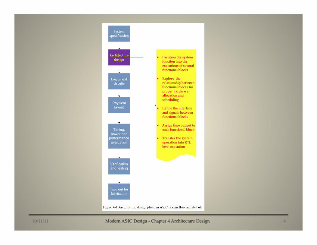
• Figure 4‑1 indicates the phase of architecture design in the design flow and highlights the involved work.
• At architecture level, functional blocks or Intellectual Properties (IPs) are considered as basic components. – In this chapter we shall study how to model and connect these
functional blocks.
• Operations of functional blocks and data flow will be coordinated by a Finite State Machine (FSM).
• The system architecture is finally described using VHDL (or Verilog) at the RTL level – It can be used for a clock cycle-by-cycle simulation, as well as
for next phase synthesis and verification.
• At the end of this chapter, an example architecture of the MSDAP is presented in detail to illustrate architecture development.

• At the top level, a digital system can be partitioned into two parts: a datapath and a controller.
• The datapath is used to store, manipulate, and transfer data, and the controller provides the command for these operations.
– Figure 4‑2 illustrates a general datapath structure, where the controller is usually an FSM; ALU is an arithmetic logic unit consisting of an adder, multiplexer and shifter; input/output interface usually is made of shift registers. The memory and bus are used to store and transfer data, respectively.


• In an ASIC architecture each functional block must be defined precisely, including its functionality, input/output pins and signals, as well as the performance requirement in terms of clock cycles.
• An architecture designer partitions the system function into sub-functions, each of them realized by a functional block.
• The architecture designer also needs to specify the control signals of each block, which controls the corresponding operation and data flow.
• In many cases, one has to use the components from a company’s existing cell library or IPs from other parties. – This adds additional constraints to the architecture design.

• The objectives of architecture design are twofold:
– to minimize hardware resources which implement the specified function while satisfying the given performance requirement, and
– to have a clean partition of the function and a clear relationship between the partitioned sub-functions which facilitates verification and testing.

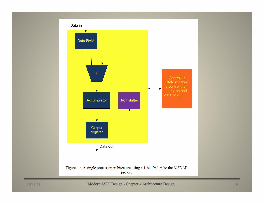
• In the single processor structure, the number of ALU units is minimal and other components are added, such as data and coefficient RAMs, and data path controllers.
• In the previous general datapath structure shown in Figure 4‑2, functional blocks are represented at a very high level, and many details are omitted.
– For instance, the ALU is a general arithmetic logic unit without implementation details.
– Even for such a simple ALU there might be more than one implementation option.

• Two possible ALU architectures for the computation of linear convolution
– A straight forward architecture without specific constraint
– An architecture with the constraint proposed by the MSDAP

• A straight forward architecture


• An architecture with the constraint

• Parallel properties are explored in the design when a single processor, for instance one ALU, doesn’t satisfy the application computation speed requirement.
• We use a pipeline structure as an example to explore the property of the multiprocessor parallel computation.
– An example
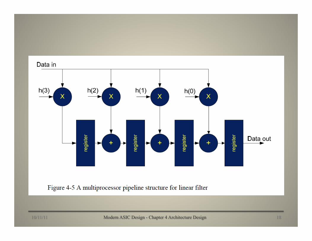
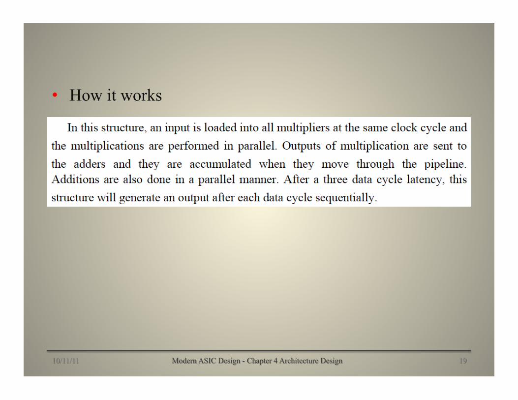
• How it works

• Operation details


• Its properties and advantages

• To demonstrate the structure variety, a slightly different version can be introduced as shown in Figure 4‑6.

• Speed-up obtained by parallel structure

• The choice between single and multi-processor structure will mainly be determined by the cost, provided that both can accomplish the specified task.
– For instance, the MSDAP project not only uses a single processor structure, but further uses a 1-bit shifter to reduce the cost, because today’s IC speeds can easily satisfy such computation needs.

• We have seen that the datapath structure consisted of functional blocks as the basic circuit elements.
• In real design practice, the complexity of these functional blocks may vary from a simple adder to a powerful microprocessor, such as an ARM core in some ASIC designs.
• Regardless of whether it is a simple or a complex functional block, it needs to be completely defined in a similar way as we define a normal ASIC chip.

• The definition should include the following basic information:
– Functionality
– Input/output pins
– Signals
– Interface requirements
– Layout area and shape specifications
– Performance requirements
– Other requirements depending on the application settings

• A general view of a functional block

• In electronic design one can use the existing functional block provided by the third party, called semiconductor intellectual property core, IP core, or IP block.
• This is a reusable unit of logic, cell, or chip layout design that is the intellectual property of another party.
• The term is derived from the licensing of the patent and source code copyright intellectual property rights that concern the design.
• IP cores are frequently used as building blocks within ASIC chip designs.

• IP cores in the electronic design industry have had a profound impact on the design of systems on a chip.
– For instance, ARM cores have been widely used in many cell phones and multimedia applications.
• By licensing a design multiple times, IP core providers spread the cost of development among multiple chip makers.
– IP cores are the re-usable functional blocks within the entire IC industry, instead of within a single IC company.
• IP cores for standard processors, interfaces, and internal functions enable chip makers to put more resources into developing the differentiating features of their chips.
– As a result, chip makers are able to develop new innovations faster.
• The licensing and use of IP cores in chip design became common practice in the 1990s.
– The microprocessor cores of ARM Holdings are recognized as some of the first widely licensed IP cores.
• It has been a popular choice for many digital applications because of its competitive time to market.
– Using such IPs we can significantly improve design efficiency and product reliability since these IP cores have been optimized and tested.

• IP cores are typically offered as synthesizable RTL netlists.
– Synthesizable cores are delivered in a hardware description language such as Verilog or VHDL.
– These are analogous to high level languages such as C in the field of computer programming.
• IP cores delivered to chip makers as RTL allow chip designers to modify designs if necessary, though many IP vendors offer no warranty or support for modified designs
– Thus modifications require extreme caution and detailed verification.

• IP cores are also sometimes offered as generic gate-level netlists. – The netlist is a Boolean-algebra representation of the IP’s
logical function implemented as generic gates or process specific cells. A gate-level netlist is analogous to an assembly-code listing in the field of computer programming.
– A netlist gives the IP core vendor reasonable protection against reverse engineering.
• Both netlist and synthesizable cores are called soft cores, because both allow a synthesis, placement and route (SPR) design flow.

• The advantage of an IP core implemented as a generic gate is that it is portable to other process technologies, if the technology is compatible.
• Because different processes might be used to implement the gates in the netlist, the timing of the logic circuit may change.
– A careful timing analysis, both static and dynamic, should be followed to ensure the correct operation.
• Analog and mixed-signal logics are generally defined as lower-level physical descriptions.
– Hence, analog IP (PLLs, DAC, ADC, etc.) are provided to chip makers in transistor-layout format such as in GDSII (GDSII 2011).
• Digital IP cores are sometimes offered in a layout format as well. Such cores, whether analog or digital, are called hard cores (or hard macros), because the core’s application function cannot be meaningfully modified by chip designers.
– Transistor layouts must obey the target foundry’s process design rules, and hence, hard cores delivered for one foundry’s process cannot be easily ported to a different process or foundry.

• Merchant foundry operators offer a variety of hard-macro IP functions built for their own foundry process, helping to ensure customer lock-in.
• Hard cores, by the nature of their low-level representation, offer better predictability of chip performance in terms of timing performance and area.

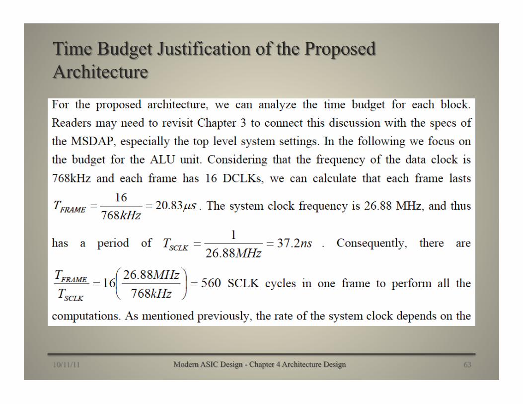
• With the presented specs and signal definitions in Chapter 3 for the MSDAP, we now show an example architecture from the project report (Patel and Hernandez-Garduno 2009).
• A high level abstraction is presented in Figure 4‑8 to facilitate the discussion of defining the functionality of each block.
– The timing information related to the detail clock is not complete since we still need more detailed structures of ALU to budget the number of operations.
• Each block is defined as required in Figure 4‑7 so that its functionality, input/output, status and control signals are precisely stated.


• Definition of the function blocks in the architecture
• Control logic definition
– The main function of the Control Logic of the MSDAP is described in Chapter 3 when discussing the system mode and settings.
• A sample VHDL code has been developed which handles the state transitions.
– In addition, this Control Logic handles all data transfers and memory reads and writes. It also handles trivial operations such as sign extension and shift operations.
– For this reason, other components in the MSDAP architecture are designed as asynchronous elements which are able to start their function within 1 Sclk cycle.
– The Control Logic also completes the task of monitoring and updating top level control signals as specified by the MSDAP specification (the operation mode in Figure 3-7, and signal format and waveform at Section 3.5.2).
• SIPO definition
– The SIPO module is the front-end data interface of the MSDAP that takes 1-bit serial data synchronous to a Data Clock and converts it to 16-bit parallel data.
– New input words are signaled by an increase in the Frame signal on the first bit of the serial frame and output words are signaled ready by an increase in the DataWordReady signal for the clock cycle, so that the word is guaranteed valid.
– The SIPO module is cleared by an active high Reset signal. Following are its I/Os and data and control signal definitions.

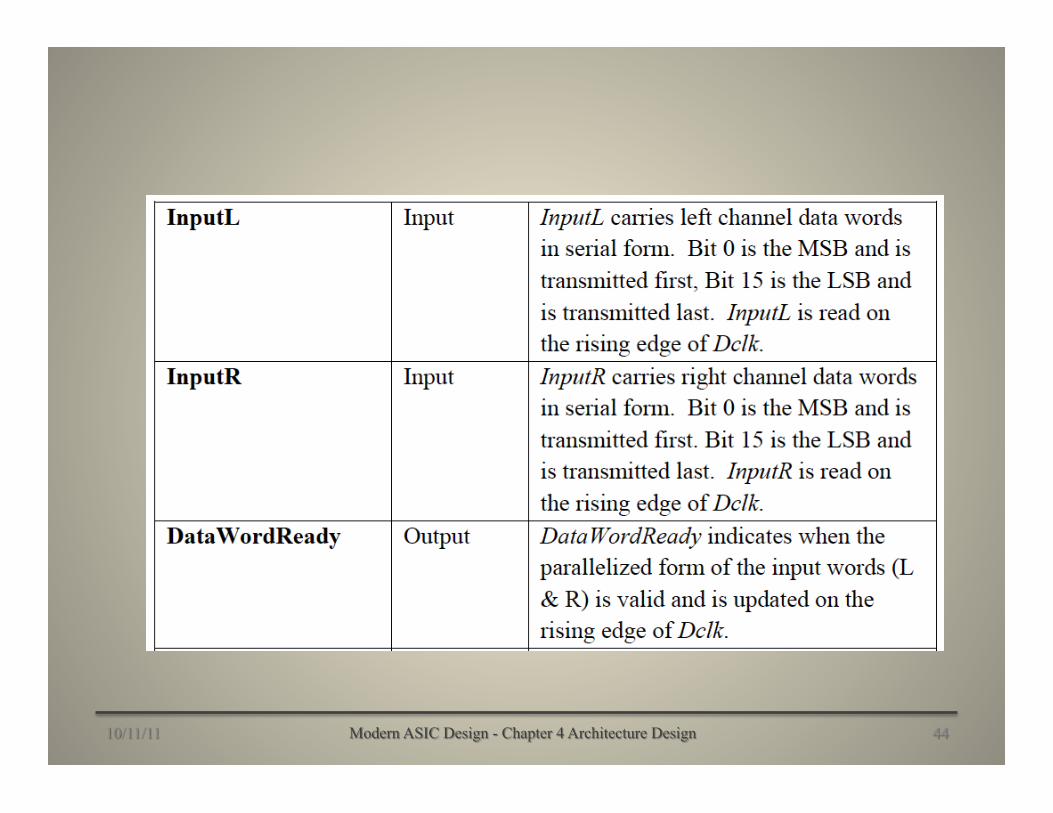
• SIPO definition (details)

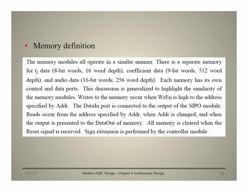
• Memory definition


• Adder/Subtracter definition


• Shift operation definition
– The shifting operation of the MSDAP is performed by the Controller FSM by reassigning the bit positions of the output of the adder when accumulating the final result and thus is not specified as a separate module.
– The DataOut signal is the final shifted result that is outputted by the PISO module.

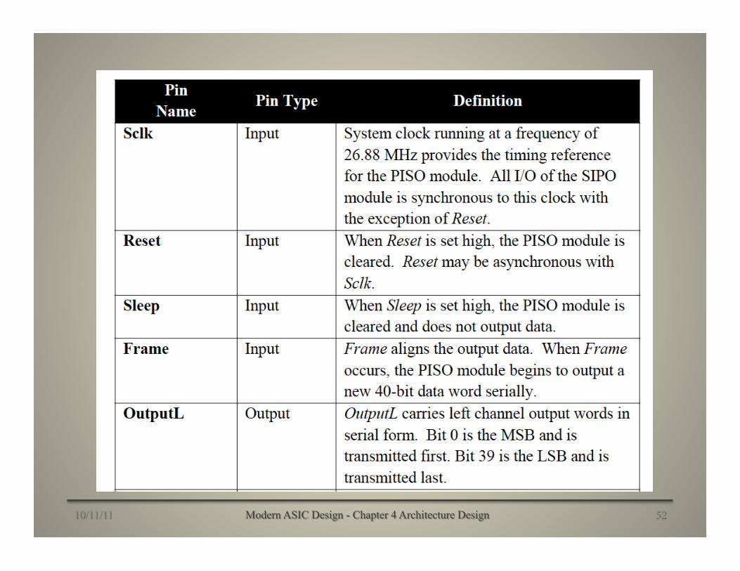
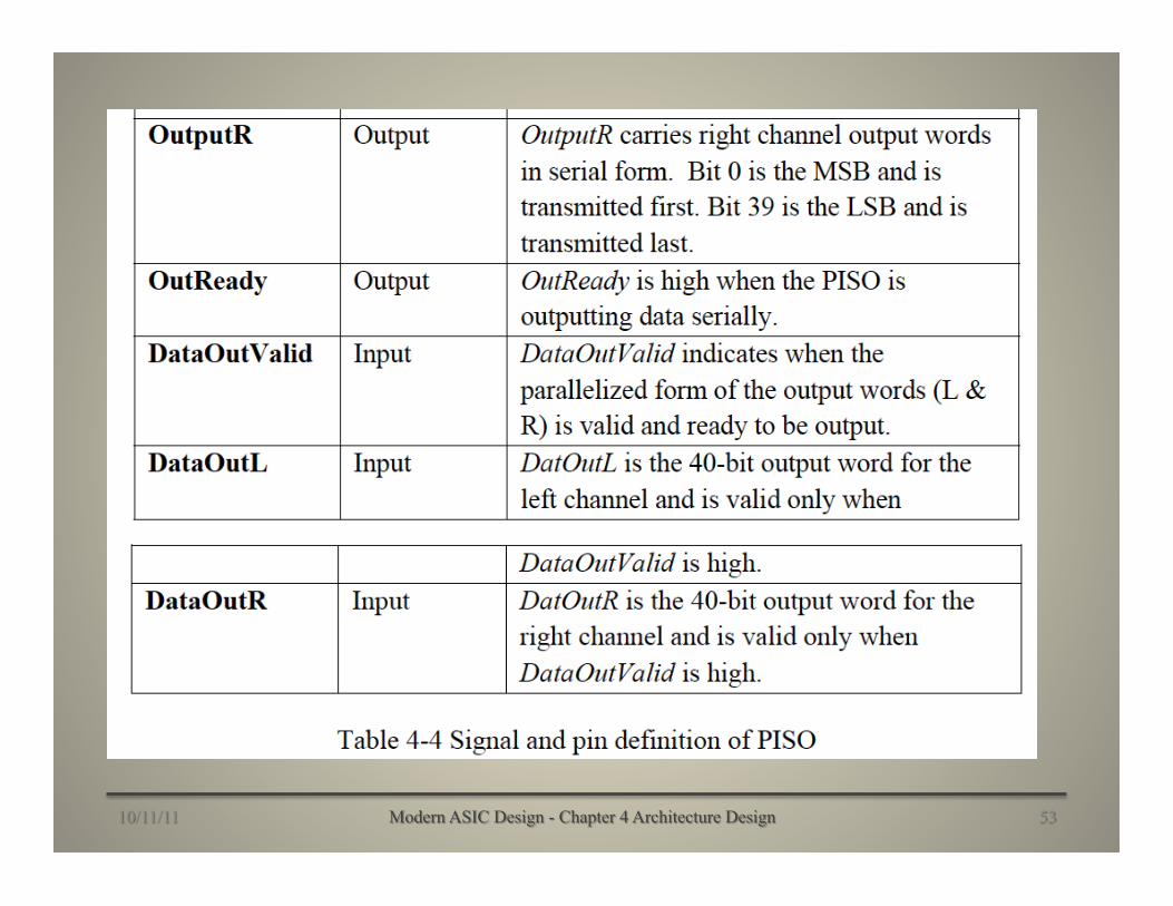
• PISO definition
– The PISO module is the data interface of the MSDAP that processes 40-bit parallel data outputs serially via a 1-bit port synchronous to Sclk upon the arrival of the next Frame signal.
– Output words are signaled ready by an increase of the DataOutValid signal.
– The OutReady signal is set high for the 40 bits that the PISO is serially outputting data.
– The SIPO module is cleared by an active high Reset signal and does not output when it receives a high Sleep signal.

• From the above example, we see how functional blocks are defined.
• With a complete definition, blocks can be assigned to different design groups and be verified individually before integrating them into the system.
• The definition of a function block also includes control signals since a block is controlled by a top level FSM. – For instance, a signal Reset is a signal from the Controller FSM
that instructs the memory, SIPO and PISO to clear their contents and set them to an initial condition.
– A functional block also usually feeds the controller information about its status. DataOutValid in the PISO block is such an instance.

• In a parallel manner, during the architecture development we not only define the functional blocks and corresponding relations, but also assign a time budget to each functional block.
• Specifically,
– Each functional block should be given adequate cycles to complete its assigned job;
– The input to each functional block must be ready when it is needed.

• Time budget is usually obtained from a process called resource allocation and scheduling.
• Resource allocation assigns computation tasks to functional blocks, and scheduling arranges these tasks in such a way that they can be executed without confliction.
• To find the time window for a task to be executed we can use the schedule techniques like as soon as possible and as late as possible.
– However, combining scheduling with optimal resource allocation is a difficult task. Most of the time, it is still a decision made based on experience.
• The time budget depends on the proposed architecture and its feasibility must be analyzed carefully in the architecture design stage.
• A structure is requisite to discussing this topic.
• In the next section we shall use the architecture of our MSDAP project to show how to allocate the time budget.

• Figure 4‑8 is a top level general datapath architecture, which we have used to assist the discussion of how to define functional blocks.
• However, architecture should be developed such that it can eventually be coded at an RTL level so that a cycle-by-cycle simulation can be carried out to verify the correctness of the digital system without involving detailed logic and circuit designs.
• The degree of detail depends on the designer, but it must be to a level where we can write VHDL code and verify the hardware design.

• In doing so, we need to do work similar to what we did in developing the specification of the MSDAP. That is, we need to define the signals and functions among the functional blocks.
– For example, in referring to the general architecture in Figure 4‑8, we do not know how to write the VHDL code since we haven’t defined the interfaces between the functional blocks.
– Therefore, one can’t tell in what way ALU works with memory and output interface blocks.
– In short, too many details are missing there.
– In the following we look at how to develop such an architecture.

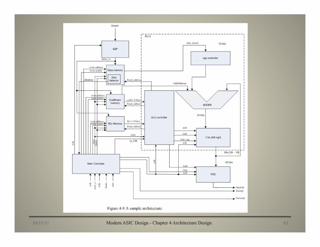
• Based on the spec, a proposed architecture for the MSDAP is shown in Figure 4‑9, which allows us to describe it in VHDL.
– Only one channel is shown here for clarity. Notice that not all the I/O pins for each functional block have been included.
– Also, the main controller is shared between the two identical datapath blocks, left and right.
– (Appendix D presents a complete version of this architecture with all detailed notations and definitions.)

• Definition of each functional block in this architecture are formally presented in the text book.
Here is the definition of Data Memory


• In this chapter we discussed how to develop an architecture based on the given application.
• The most popular architecture is a datapath which consists of control logic, input/output, and an ALU unit.
• These blocks can be further partitioned into smaller functional blocks to facilitate a clear and accurate definition of timing and operation.
– Such level of detail is necessary for an accurate analysis of timing budget.
• Final architecture should be described at the RTL level for synthesis and verification.
• A sample architecture for the MSDAP is given to illustrate the concepts mentioned in the discussion.
– VHDL codes of the main blocks of the sample architecture are given to show how to accurately describe each functional block without any human language ambiguity, since such code can be simulated for verification.
• The whole design of the MSDAP, including its architecture, is given in Appendix D, from which the interested reader can have a complete picture of the design process.

• This chapter also discussed how to explore the parallelism by using multiple processors. – The key issue is to properly align the data and operations to
obtain the maximum speed-up.
• The optimal design is if all processors are doing the necessary computations and not being idle.
• Optimal scheduling and resource allocation is the key for a good architecture. – This topic has been studied extensively in high-level
synthesis. Readers who are interested in this topic can check the research literatures on this subject and find the state-of-the-art CAD tools to assist architecture design.
1. Explain how to define function blocks in architecture design. Try to formalize the method and give an example.
2. Give an example to show how data and computation dependency prevents us from achieving linear speed-up.
3. Summarize the method of architecture development in ASIC design.
4. Synthesizing a behavior model to get an RTL level netlist needs an “underlined architecture”, for any non-trivial application. Discuss this issue using an example.
5. Discuss why architecture design automation is extremely difficult. Suggest the method to solve this problem.
6. Develop an architecture of the MSDAP. 7. Explain the issue of “resource allocation” and “scheduling” in the
architecture design. Use the architecture if MSDAP as an example.