Ashley Brinker Karen Joseph Mehdi Kabir ECE 6332 – VLSI Fall 2010.
21
Ashley Brinker Karen Joseph Mehdi Kabir ECE 6332 – VLSI Fall 2010
-
Upload
amberlynn-walton -
Category
Documents
-
view
217 -
download
0
Transcript of Ashley Brinker Karen Joseph Mehdi Kabir ECE 6332 – VLSI Fall 2010.

Ashley BrinkerKaren JosephMehdi Kabir
ECE 6332 – VLSIFall 2010

• Motivation & Approach •Input Vector Control • MTCMOS
• 16-bit Adder • Results
• Conclusion
Outline

Idle Leakage CurrentGate Leakage Subthreshold Leakage
• MOSFET gate cannot completely turn off the drain-source current in transistor.
• Due to various factors such as weak inversion, carrier concentration gradients, and thermal effects.
• Current through the transistor caused by band-to-band tunneling of carriers through the gate.
• Occurs when there is a large VGS or VDG bias.
0
1
0
0
0
1
0
1
1
1
0
0

Motivation
130 90 65 45 3215
20
25
30
35
40
Process Size (nm)
Gate
Lea
kage
(%)
• As transistors are scaled down, gate leakage becomes a larger proportion of the total leakage.
• Using subthreshold reduction techniques can sometimes lead to an increase in gate leakage or vice versa.
• In many cases, better leakage reductions can be achieved by optimizing gate leakage current first.

Methodology
• First tried to optimize circuit using input vector control. • Heurisitic for determining an optimal input vector for arbitrary circuit.
• Looked at MTCMOS as a method of reducing subthreshold leakage and gate leakage.
• Analyzed tradeoffs between leakage reduction and delay.
• Applied it to a complex circuit: 16-bit ripple carry adder.

Leakage Minimization: Input Vector Control
• Leakage current is data dependent. Input vector control chooses the best input that minimizes the total leakage.
• As process size is decreased, gate leakage becomes a more significant portion of the total leakage.
130nm NAND3 gate 32nm NAND3 gate
000 001 010 011 100 101 110 1110
1
2
3
4
5
6
7
8x 10
-8
Input Vector
Curr
ent (
A)
000 001 010 011 100 101 110 1110
0.2
0.4
0.6
0.8
1
1.2
1.4
1.6x 10
-8
Input Vector
Curr
ent (
A)
SubthresholdGate

Optimum Input Vector
• Finding the optimum input vector for an arbitrary circuit is a NP-complete problem.
• Possible Solution: Use exhaustive search to find best vector. Not useful for circuits with large number of inputs.
• Near-optimal Solution: For large circuits using a Monte Carlo search or genetic algorithms can yield input vectors which are better than average.
• Near-optimal Solution: Use a type of greedy search heuristic to find the input vector which minimizes a cost function.

Optimum Input Vector
Heuristic Outline
1Generate a node controllability list for each node in circuit.
2Find the best case input for each gate in circuit based on total leakage and node controllability.
3 Determine conflicting and dominating cells.
4Use a cost function which penalizes gates not in best case input or ones which force conflicts and rewards gates which dominate the most of the other cells.
5Choose gate with the minimum cost function and satisfy its best case input. Repeat process until all input vectors are set to a value.
2-input XOR gate
00 01 10 110
0.5
1
1.5
2
2.5
3
3.5x 10
-8
Input Vector
Leak
age C
urre
nt (A
)
SubthresholdGate

Optimum Input Vector: Example

Optimum Input Vector: Full AdderProcess Size Optimal Input Mean Leakage
Reduction
130 nm A=0000 0000 0000 0000B=0000 0000 0000 0000
Cin=0
17.6%
32 nm A=0000 0000 0000 0000B=1010 1010 1010 1010
Cin=1
28.3%
0
0.1
0.2
0.3
0.4
0.5
0.6
0.7
0.8
0.9
1x 10
-6
Input Vectors
Leak
age
Curr
ent (
A)
SubthreholdGate
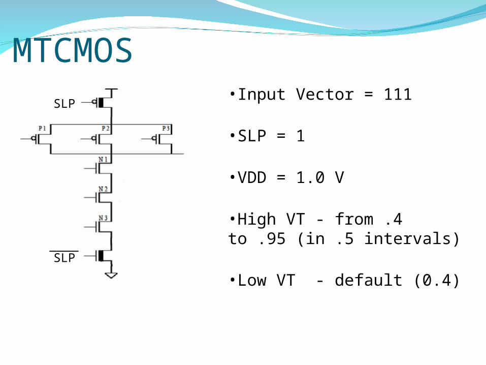
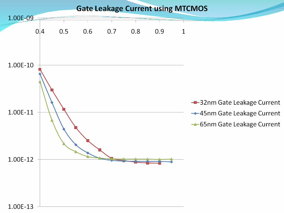
MTCMOS•Input Vector = 111
•SLP = 1
•VDD = 1.0 V
•High VT - from .4 to .95 (in .5 intervals)
•Low VT - default (0.4) SLP
SLP
____


Current x (Delay)2

Optimal VT

Optimizing Total Leakage: Gate Replacement
• Minimize gate leakage by using input vector control to choose the optimal inputs.
• The total leakage is usually concentrated in a few of the gates.
• Replace those gates with MTCMOS to further reduce the subthreshold leakage in those gates.
9.4nA3.4nA
2.5nA
18.9nA
5.7nA
3.4nA
2.5nA5.7nA
6.6nA
12.7nA

Optimizing Total Leakage: Results
Process Size
Optimal Input Mean Leakage
Reduction
Mean Leakage Reduction (MTCMOS)
Mean Delay Increase
130 nm A=0000 0000 0000 0000B=0000 0000 0000 0000
Cin=0
17.6% 28.9% 3.2%
90 nm A=0000 0000 0000 0000B=0000 0000 0000 0000
Cin=0
19.4% 30.4% 3.4%
65 nm A=0000 0000 0000 0000B=0000 0000 0000 0000
Cin=0
21.5% 33.9% 3.4%
45 nm A=0000 0000 0000 0000B=1010 1010 1010 1010
Cin=1
25.3% 41.8% 4.7%
32 nm A=0000 0000 0000 0000B=1010 1010 1010 1010
Cin=1
28.3% 45.2% 5.6%

Conclusions
• Gate leakage plays a significant role in leakage current as the technology size is scaled down and it must be taken into account when using leakage reduction techniques.
• Input vector control along with the use of stacking and threshold voltage control can be used effectively to reduce both subthreshold and gate leakage current.
• Heuristics can be extended to arbitrary circuits to optimize the total leakage current.
• Further work can be done on sizing the transistors to improve leakage current.

Questions?