
ARM Dual-Timer Module (SP804)infocenter.arm.com/help/topic/com.arm.doc.ddi0271d/DDI0271.pdf · ARM...
54
Copyright © 2002-2004 ARM Limited. All rights reserved. ARM DDI 0271D ARM Dual-Timer Module (SP804) Revision: r1p0 Technical Reference Manual
Transcript of ARM Dual-Timer Module (SP804)infocenter.arm.com/help/topic/com.arm.doc.ddi0271d/DDI0271.pdf · ARM...

ARM Dual-Timer Module (SP804)Revision: r1p0
Technical Reference Manual
Copyright © 2002-2004 ARM Limited. All rights reserved.ARM DDI 0271D

ARM Dual-Timer Module (SP804)Technical Reference Manual
Copyright © 2002-2004 ARM Limited. All rights reserved.
Release Information
Proprietary Notice
Words and logos marked with ® or ™ are registered trademarks or trademarks of ARM Limited in the EU and other countries, except as otherwise stated below in this proprietary notice. Other brands and names mentioned herein may be the trademarks of their respective owners.
Neither the whole nor any part of the information contained in, or the product described in, this document may be adapted or reproduced in any material form except with the prior written permission of the copyright holder.
The product described in this document is subject to continuous developments and improvements. All particulars of the product and its use contained in this document are given by ARM Limited in good faith. However, all warranties implied or expressed, including but not limited to implied warranties of merchantability, or fitness for purpose, are excluded.
This document is intended only to assist the reader in the use of the product. ARM Limited shall not be liable for any loss or damage arising from the use of any information in this document, or any error or omission in such information, or any incorrect use of the product.
Confidentiality Status
This document is Non-Confidential. The right to use, copy and disclose this document may be subject to license restrictions in accordance with the terms of the agreement entered into by ARM and the party that ARM delivered this document to.
Product Status
The information in this document is final, that is for a developed product.
Web Address
http://www.arm.com
Change history
Date Issue Change
31 October 2002 A First release
26 June 2003 B Signal name changes and TimerPeriphID2 Register value
14 November 2003 C Change security to Open Access
23 January 2004 D Value changed in Example 2-1
ii Copyright © 2002-2004 ARM Limited. All rights reserved. ARM DDI 0271D

ContentsARM Dual-Timer Module (SP804) Technical Reference Manual
PrefaceAbout this book .............................................................................................. xFeedback ..................................................................................................... xiv
Chapter 1 Introduction1.1 About the ARM Dual-Timer module (SP804) .............................................. 1-21.2 Features ...................................................................................................... 1-31.3 Programmable parameters ......................................................................... 1-4
Chapter 2 Functional Overview2.1 Overview ..................................................................................................... 2-22.2 Functional description ................................................................................. 2-4
Chapter 3 Programmer’s Model3.1 Summary of registers .................................................................................. 3-23.2 Register descriptions .................................................................................. 3-4
Chapter 4 Programmer’s Model for Test4.1 Integration test harness overview ............................................................... 4-24.2 Scan testing ................................................................................................ 4-3
ARM DDI 0271D Copyright © 2002-2004 ARM Limited. All rights reserved. iii
Contents
4.3 Test registers .............................................................................................. 4-4
Appendix A Signal DescriptionsA.1 AMBA APB signals ..................................................................................... A-2A.2 Non-AMBA signals ..................................................................................... A-3
iv Copyright © 2002-2004 ARM Limited. All rights reserved. ARM DDI 0271D

List of TablesARM Dual-Timer Module (SP804) Technical Reference Manual
Change history .............................................................................................................. iiTable 2-1 Expressions for calculating timer intervals .............................................................. 2-13Table 3-1 Summary of registers ................................................................................................ 3-2Table 3-2 Control Register bit assignments .............................................................................. 3-5Table 3-3 Raw Interrupt Status Register bit assignments ......................................................... 3-6Table 3-4 Masked Interrupt Status Register bit assignments .................................................... 3-7Table 3-5 Peripheral Identification Register options .................................................................. 3-7Table 3-6 Timer Peripheral ID0 Register bit assignments ......................................................... 3-9Table 3-7 Timer Peripheral ID1 Register bit assignments ......................................................... 3-9Table 3-8 Timer Peripheral ID2 Register bit assignments ......................................................... 3-9Table 3-9 TimerPeriphID3 register bit assignments ................................................................ 3-10Table 3-10 PrimeCell ID0 Register bit assignments .................................................................. 3-11Table 3-11 PrimeCell ID1 Register bit assignments .................................................................. 3-11Table 3-12 PrimeCell ID2 Register bit assignments .................................................................. 3-11Table 3-13 PrimeCell ID3 Register bit assignments .................................................................. 3-12Table 4-1 Integration Test Control Register bit assignments .................................................... 4-4Table 4-2 Integration Test Output Set Register bit assignments ............................................... 4-4Table A-1 AMBA APB signal descriptions ................................................................................. A-2Table A-2 Non-AMBA signals .................................................................................................... A-3
ARM DDI 0271D Copyright © 2002-2004 ARM Limited. All rights reserved. v
List of Tables
vi Copyright © 2002-2004 ARM Limited. All rights reserved. ARM DDI 0271D
List of FiguresARM Dual-Timer Module (SP804) Technical Reference Manual
Figure 1-1 Simplified block diagram ........................................................................................... 1-3Figure 2-1 Dual-Timer module block diagram ............................................................................ 2-4Figure 2-2 TIMCLK equals PCLK and TIMCLKENX equals one, clock example ....................... 2-7Figure 2-3 TIMCLK equals PCLK and TIMCLKENX is pulsed, clock example ........................... 2-7Figure 2-4 TIMCLK is less than PCLK and TIMCLKENX equals one, clock example ................ 2-7Figure 2-5 TIMCLK is less than PCLK and TIMCLKENX is pulsed, clock example ................... 2-8Figure 2-6 Prescale clock enable generation ............................................................................. 2-8Figure 2-7 Example timing diagram of prescaler clock enable generation ................................. 2-9Figure 2-8 Example interrupt signal timing ............................................................................... 2-12Figure 2-9 Raw and masked interrupt status ............................................................................ 2-12Figure 3-1 Peripheral identification register bit assignment ........................................................ 3-8Figure 3-2 PrimeCell identification register bit assignments ..................................................... 3-10Figure 4-1 Output integration test harness ................................................................................. 4-2
ARM DDI 0271D Copyright © 2002-2004 ARM Limited. All rights reserved. vii

List of Figures
viii Copyright © 2002-2004 ARM Limited. All rights reserved. ARM DDI 0271D

Preface
This preface introduces the Dual-Timer module (SP804) and its reference documentation. It contains the following sections:
• About this book on page x
• Feedback on page xiv.
ARM DDI 0271D Copyright © 2002-2004 ARM Limited. All rights reserved. ix

Preface
About this book
This document is the Technical Reference Manual (TRM) for the ARM Dual-Timer module (SP804).
Intended audience
This document in intended for hardware and software engineers implementing System-on-Chip (SoC) designs.
Using this book
This book is organized into the following chapters:
Chapter 1 Introduction
Read this chapter for an introduction to the Dual-Timer module and its features.
Chapter 2 Functional Overview
Read this chapter for an overview of the major functional blocks and the operation of the Dual-Timer module.
Chapter 3 Programmer’s Model
Read this chapter for a description of the registers and for details of system initialization.
Chapter 4 Programmer’s Model for Test
Read this chapter for a description of the additional logic for functional verification and production testing.
Appendix A Signal Descriptions
Read this appendix for a description of the Dual-Timer module signals.
Product revision status
The rnpn identifier indicates the revision status of the product described in this document, where:
rn Identifies the major revision of the product.
pn Identifies the minor revision or modification status of the product.
x Copyright © 2002-2004 ARM Limited. All rights reserved. ARM DDI 0271D

Preface
Typographical conventions
The following typographical conventions are used in this book:
italic Highlights important notes, introduces special terminology, denotes internal cross-references, and citations.
bold Highlights interface elements, such as menu names. Denotes ARM processor signal names. Also used for terms in descriptive lists, where appropriate.
monospace Denotes text that can be entered at the keyboard, such as commands, file and program names, and source code.
monospace Denotes a permitted abbreviation for a command or option. The underlined text can be entered instead of the full command or option name.
monospace italic Denotes arguments to commands and functions where the argument is to be replaced by a specific value.
monospace bold Denotes language keywords when used outside example code.
Other conventions
This document uses other conventions. They are described in the following sections:
• Signals
• Bytes, Halfwords, and Words on page xii
• Bits, bytes, k, and M on page xii
• Register fields on page xii.
Signals
When a signal is described as being asserted, the level depends on whether the signal is active HIGH or active LOW. Asserted means HIGH for active high signals and LOW for active low signals:
Prefix n Active LOW signals are prefixed by a lowercase n except in the case of AHB or APB reset signals. These are named HRESETn and PRESETn respectively.
Prefix H AHB signals are prefixed by an upper case H.
Prefix P APB signals are prefixed by an upper case P.
ARM DDI 0271D Copyright © 2002-2004 ARM Limited. All rights reserved. xi

Preface
Bytes, Halfwords, and Words
Byte Eight bits.
Halfword Two bytes (16 bits).
Word Four bytes (32 bits).
Quadword 16 contiguous bytes (128 bits).
Bits, bytes, k, and M
Suffix b Indicates bits.
Suffix B Indicates bytes.
Suffix K When used to indicate an amount of memory means 1024. When used to indicate a frequency means 1000.
Suffix M When used to indicate an amount of memory means 10242 = 1048 576. When used to indicate a frequency means 1000000.
Register fields
All reserved or unused address locations must not be accessed as this can result in unpredictable behavior of the device.
All reserved or unused bits of registers must be written as zero, and ignored on read unless otherwise stated in the relevant text.
All registers bits are reset to logic 0 by a system reset unless otherwise stated in the relevant text.
Unless otherwise stated in the relevant text, all registers support read and write accesses. A write updates the contents of the register and a read returns the contents of the register.
All registers defined in this document can only be accessed using word reads and word writes, unless otherwise stated in the relevant text.
Numbers
The conventions used in this document for numbers are:
Prefix b Binary numbers are prefixed by a lowercase b.
Prefix 0x Hexadecimal numbers are prefixed by 0x and use a monospace font.
xii Copyright © 2002-2004 ARM Limited. All rights reserved. ARM DDI 0271D

Preface
Further reading
This section lists publications from ARM Limited that provide additional information about ARM devices.
ARM periodically provides updates and corrections to its documentation. See http://www.arm.com for current errata sheets and addenda, and also for ARM Frequently Asked Questions.
ARM publications
This document contains information that is specific to the ARM Dual-Timer module. Refer to the following document for other relevant information:
• AMBA Specification (Rev 2.0) (ARM IHI 0011).
ARM DDI 0271D Copyright © 2002-2004 ARM Limited. All rights reserved. xiii
Preface
Feedback
ARM Limited welcomes feedback on both the Dual-Timer Module (SP804), and its documentation.
Feedback on the Dual-Timer Module (SP804)
If you have any problems with the Dual-Timer Module (SP804), contact your supplier. To help us provide a rapid and useful response, give:
• details of the release you are using
• details of the platform you are running on, such as the hardware platform, operating system type and version
• a small standalone sample of code that reproduces the problem
• a clear explanation of what you expected to happen, and what actually happened
• the commands you used, including any command-line options
• sample output illustrating the problem
• the version string of the tool, including the version number and date.
Feedback on this book
If you have any comments on this book, send email to [email protected] giving:
• the document title
• the document number
• the page number(s) to which your comments apply
• a concise explanation of your comments.
General suggestions for additions and improvements are also welcome.
xiv Copyright © 2002-2004 ARM Limited. All rights reserved. ARM DDI 0271D

Chapter 1 Introduction
This chapter introduces the Dual-Timer Module (SP804). It contains the following sections:
• About the ARM Dual-Timer module (SP804) on page 1-2
• Features on page 1-3
• Programmable parameters on page 1-4.
ARM DDI 0271D Copyright © 2002-2004 ARM Limited. All rights reserved. 1-1

Introduction
1.1 About the ARM Dual-Timer module (SP804)
The ARM Dual-Timer module is an Advanced Microcontroller Bus Architecture (AMBA) compliant System-on-Chip (SoC) peripheral developed, tested and licensed by ARM Limited. For more information, see the AMBA Specification (Rev 2.0).
The module is an AMBA slave module and connects to the Advanced Peripheral Bus (APB). The Dual-Timer module consists of two programmable 32/16-bit down counters that can generate interrupts on reaching zero.
1-2 Copyright © 2002-2004 ARM Limited. All rights reserved. ARM DDI 0271D

Introduction
1.2 Features
The features of the Dual-Timer module are:
• Compliance to the AMBA Specification (Rev 2.0) for easy integration into an SoC implementation.
• Two 32/16-bit down counters with free-running, periodic and one-shot modes.
• Common clock with separate clock-enables for each timer gives flexible control of the timer intervals.
• Interrupt output generation on timer count reaching zero.
• Identification registers that uniquely identify the Dual-Timer module. These can be used by software to automatically configure itself.
Figure 1-1 shows a simplified block diagram of the module.
Note In Figure 1-1, test logic is not shown for clarity.
Figure 1-1 Simplified block diagram
ID registers
Integration test registers
AMBA APB
signals
AMBA APB Interface Load Register
Value Register
Background load Register
Control Register
Raw Interrupt Status Register
Masked Interrupt Status Register
Interrupt Clear Register
32/16-bit down counterPrescaler
Timer 1 Free Running Counter
TIMCLK
TIMCLKEN1
TIMCLKEN2
Load Register
Value Register
Background load Register
Control Register
Raw Interrupt Status Register
Masked Interrupt Status Register
Interrupt Clear Register
32/16-bit down counterPrescaler
Timer 2 Free Running Counter
TIMINT1
TIMINT2
TIMINTC
ARM DDI 0271D Copyright © 2002-2004 ARM Limited. All rights reserved. 1-3

Introduction
1.3 Programmable parameters
The following Dual-Timer module parameters are programmable:
• free-running, periodic, or one-shot timer modes
• 32-bit or 16-bit timer operation
• prescaler divider of 1, 16, or 256
• interrupt generation enable and disable
• interrupt masking.
1-4 Copyright © 2002-2004 ARM Limited. All rights reserved. ARM DDI 0271D

Chapter 2 Functional Overview
This chapter describes the Dual-Timer Module (SP804) operation. It contains the following sections:
• Overview on page 2-2
• Functional description on page 2-4.
ARM DDI 0271D Copyright © 2002-2004 ARM Limited. All rights reserved. 2-1

Functional Overview
2.1 Overview
This section gives a basic overview of the Dual-Timer module operation. See Functional description on page 2-4 for a full description of the Dual-Timer module functionality.
The Dual-Timer module consists of two identical programmable Free Running Counters (FRCs) that can be configured for 32-bit or 16-bit operation and one of three timer modes;
• free-running
• periodic
• one-shot.
The FRCs operate from a common timer clock, TIMCLK with each FRC having its own clock enable input, TIMCLKEN1 and TIMCLKEN2. Each FRC also has a prescaler that can divide down the enabled TIMCLK rate by 1, 16, or 256. This enables the count rate for each FRC to be controlled independently using their individual clock enables and prescalers.
TIMCLK can be equal to or be a submultiple of the PCLK frequency. However, the positive edges of TIMCLK and PCLK must be synchronous and balanced.
The operation of each Timer module is identical. A Timer module can be programmed for a 32-bit or 16-bit counter size and one of three timer modes using the Control Register. The three timer modes are:
Free-running The counter operates continuously and wraps around to its maximum value each time that it reaches zero.
Periodic The counter operates continuously by reloading from the Load Register each time that the counter reaches zero.
One-shot The counter is loaded with a new value by writing to the Load Register. The counter decrements to zero and then halts until it is reprogrammed.
The timer count is loaded by writing to the Load Register and, if enabled, the timer count decrements at a rate determined by TIMCLK, TIMCLKENX, and the prescaler setting. When the Timer counter is already running, writing to the Load Register causes the counter to immediately restart from the new value.
An alternative way of loading the Timer count is by writing to the Background Load Register. This has no immediate effect on the current count but the counter continues to decrement. On reaching zero, the Timer count is reloaded from the new load value if it is in periodic mode.
2-2 Copyright © 2002-2004 ARM Limited. All rights reserved. ARM DDI 0271D

Functional Overview
When the Timer count reaches zero an interrupt is generated. The interrupt is cleared by writing to the Interrupt Clear Register. The external interrupt signals can be masked off by the Interrupt Mask Registers.
The current counter value can be read from the Value Register at any time.
ARM DDI 0271D Copyright © 2002-2004 ARM Limited. All rights reserved. 2-3
Functional Overview
2.2 Functional description
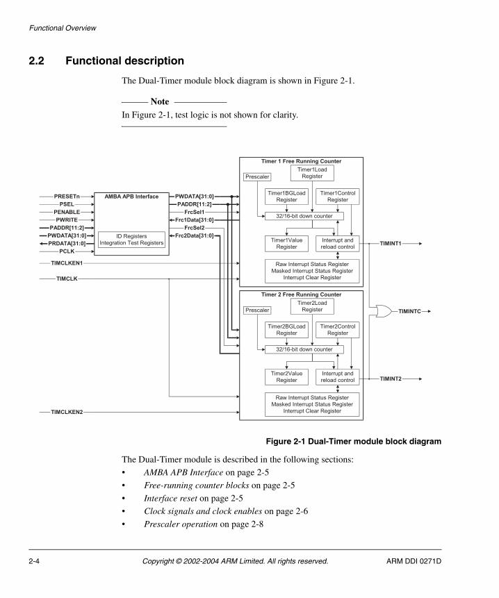
The Dual-Timer module block diagram is shown in Figure 2-1.
Note In Figure 2-1, test logic is not shown for clarity.
Figure 2-1 Dual-Timer module block diagram
The Dual-Timer module is described in the following sections:
• AMBA APB Interface on page 2-5
• Free-running counter blocks on page 2-5
• Interface reset on page 2-5
• Clock signals and clock enables on page 2-6
• Prescaler operation on page 2-8
PWDATA[31:0]
PADDR[11:2]
FrcSel1
Frc1Data[31:0]
FrcSel2
Frc2Data[31:0]
Timer 1 Free Running Counter
Prescaler
Timer1BGLoad
Register
Timer1Load
Register
Timer1Control
Register
32/16-bit down counter
Timer1Value
Register
Interrupt and
reload control
Raw Interrupt Status Register
Masked Interrupt Status Register
Interrupt Clear Register
Timer 2 Free Running Counter
Prescaler
Timer2BGLoad
Register
Timer2Load
Register
Timer2Control
Register
32/16-bit down counter
Timer2Value
Register
Interrupt and
reload control
Raw Interrupt Status Register
Masked Interrupt Status Register
Interrupt Clear Register
TIMCLKEN1
TIMCLK
TIMCLKEN2
TIMINT1
TIMINT2
TIMINTC
ID Registers
Integration Test Registers
AMBA APB Interface
PCLK
PRDATA[31:0]
PWDATA[31:0]
PADDR[11:2]
PWRITE
PENABLE
PSEL
PRESETn
2-4 Copyright © 2002-2004 ARM Limited. All rights reserved. ARM DDI 0271D

Functional Overview
• Timer operation on page 2-9
• Interrupt behavior on page 2-11
• Programming the timer interval on page 2-12
• Identification Registers on page 2-14.
2.2.1 AMBA APB Interface
The AMBA APB slave interface generates read and write decodes for accesses to all registers in the Dual-Timer module.
2.2.2 Free-running counter blocks
The two FRCs are identical and contain the 32/16-bit down counter and interrupt functionality. The counter logic is clocked independently of PCLK by TIMCLK in conjunction with a clock enable TIMCLKENX although there are constraints on the relationship between PCLK and TIMCLK. See Clock signals and clock enables on page 2-6 for details of these constraints.
Although the two FRCs are driven from a common clock, TIMCLK, each timer count rate can be independently controlled by their respective clock enables, TIMCLKEN1 and TIMCLKEN2. The prescaler in each FRC gives a further independent control of the count rate of each FRC.
See Timer operation on page 2-9 for an operational description of the FRCs.
2.2.3 Interface reset
The Dual-Timer module is reset by the global reset signal PRESETn.
PRESETn can be asserted asynchronously to PCLK but must be deasserted synchronously to the rising edge of PCLK. PRESETn is used to reset the state of the Dual-Timer module registers. The Dual-Timer module requires that PRESETn is asserted LOW for at least one period of PCLK. The values of the registers after reset are described in Chapter 3 Programmer’s Model. In summary, the Timer is initialized to the following state after reset:
• the counter is disabled
• free-running mode is selected
• 16-bit counter mode is selected
• prescalers are set to divide by 1
• interrupts are cleared but enabled
• the Load Register is set to zero
• the counter Value is set to 0xFFFFFFFF.
ARM DDI 0271D Copyright © 2002-2004 ARM Limited. All rights reserved. 2-5
Functional Overview
2.2.4 Clock signals and clock enables
The Dual-Timer module uses two input clocks:
• PCLK is used to time all APB accesses to the Dual-Timer module registers.
• TIMCLK is qualified by the clock enables, TIMCLKEN1 and TIMCLKEN2, and used to clock the prescalers, counters and their associated interrupt logic. This qualified TIMCLK rate is referred to as the effective timer clock rate. The prescaler counter only decrements on a rising edge of TIMCLK when TIMCLKENX is HIGH. The Timer counter only decrements on a rising edge of TIMCLK when TIMCLKENX is HIGH and the prescaler counter generates an enable (see Prescaler operation on page 2-8).
The relationship between TIMCLK and PCLK must observe the following constraints:
• the rising edges of TIMCLK must be synchronous and balanced with a rising edge of PCLK
• TIMCLK frequency cannot be greater than PCLK frequency.
TIMCLK, TIMCLKEN1, and TIMCLKEN2 can be used in the ways described in the following sections:
• TIMCLK equals PCLK and TIMCLKENX equals one
• TIMCLK equals PCLK and TIMCLKENX is pulsed on page 2-7
• TIMCLK is less than PCLK and TIMCLKENX equals one on page 2-7
• TIMCLK is less than PCLK and TIMCLKENX is pulsed on page 2-8.
Note Unless otherwise stated these examples use a prescale setting of divide by 1. The examples apply to either Timer1 or Timer2 in the module. TIMCLKENX refers to either TIMCLKEN1 or TIMCLKEN2.
TIMCLK equals PCLK and TIMCLKENX equals one
Figure 2-2 on page 2-7 shows the case where TIMCLK is identical to PCLK and TIMCLKENX is permanently enabled. In this case, the counter is decremented on every TIMCLK edge.
2-6 Copyright © 2002-2004 ARM Limited. All rights reserved. ARM DDI 0271D

Functional Overview
Figure 2-2 TIMCLK equals PCLK and TIMCLKENX equals one, clock example
TIMCLK equals PCLK and TIMCLKENX is pulsed
Figure 2-3 shows the case where TIMCLK is identical to PCLK but TIMCLKENX only enables every second TIMCLK edge. In this case, the counter is decremented on every second TIMCLK rising edge.
Figure 2-3 TIMCLK equals PCLK and TIMCLKENX is pulsed, clock example
TIMCLK is less than PCLK and TIMCLKENX equals one
Figure 2-4 shows the case where TIMCLK frequency is a submultiple of the PCLK frequency but the rising edges of TIMCLK are synchronous and balanced with PCLK edges. TIMCLKENX is permanently enabled. In this case, the counter is decremented on every TIMCLK rising edge.
Figure 2-4 TIMCLK is less than PCLK and TIMCLKENX equals one, clock example
PCLK
TIMCLK
TIMCLKENX=1
n n-1 n-2Count
PCLK
TIMCLK
TIMCLKENX
n-1Count n n-2
PCLK
TIMCLK
TIMCLKENX=1
n n-1Count
ARM DDI 0271D Copyright © 2002-2004 ARM Limited. All rights reserved. 2-7

Functional Overview
TIMCLK is less than PCLK and TIMCLKENX is pulsed
Figure 2-5 shows the case where TIMCLK frequency is a submultiple of the PCLK frequency but the rising edges of TIMCLK are synchronous and balanced with PCLK edges. TIMCLKENX only enables every second TIMCLK edge. In this case, the counter is decremented on every second TIMCLK rising edge.
Figure 2-5 TIMCLK is less than PCLK and TIMCLKENX is pulsed, clock example
2.2.5 Prescaler operation
The prescaler generates a timer clock enable that is used to enable the decrementing of the timer counter at one of the following rates:
• the effective timer clock rate where TIMCLK is qualified by TIMCLKENX• the effective timer clock rate divided by 16
• the effective timer clock rate divided by 256.
Figure 2-6 shows how the timer clock enable is generated by the prescaler.
Figure 2-6 Prescale clock enable generation
Figure 2-7 on page 2-9 shows an example of how the prescaler generates the timer clock enable for a prescaler setting of divide by 16.
PCLK
TIMCLK
TIMCLKENX
n-1Count n n-2
Timer clock
enable
(TIMCLKENX)
Divide by 16 Divide by 16
TimerX Control
RegisterTimerPre[1:0]
Timer clock enable
after prescaling00
01
10
2-8 Copyright © 2002-2004 ARM Limited. All rights reserved. ARM DDI 0271D

Functional Overview
Figure 2-7 Example timing diagram of prescaler clock enable generation
2.2.6 Timer operation
After the initial application and release of PRESETn, the Timer state is initialized as follows:
• the counter is disabled, TimerEn=0
• free-running mode is selected, TimerMode=0 and OneShot=0
• 16-bit counter mode is selected, TimerSize=0
• prescalers are set to divide by 1, TimerPre=0x0
• interrupts are cleared but enabled, IntEnable=1
• the Load Register is set to zero
• the counter Value is set to 0xFFFFFFFF.
The operation in each of the three Timer modes is described in:
• Free-running mode
• Periodic mode on page 2-10
• One-shot mode on page 2-11.
Free-running mode
Free-running mode is selected by setting the following bits in the TimerControl Register:
• set TimerMode bit to 1
• set OneShot bit to 0.
The 32-bit or 16-bit counter operation is selected by setting the TimerSize bit appropriately in the TimerControl Register.
16 enabled TIMCLKs
PCLK
TIMCLK
TIMCLKENX
Prescaler enable
(divide by 16)
Count
16 enabled TIMCLKs
n-1n n-2 n-3
ARM DDI 0271D Copyright © 2002-2004 ARM Limited. All rights reserved. 2-9

Functional Overview
On reset the timer value is initialized to 0xFFFFFFFF and if the counter is enabled then the count decrements by one for each TIMCLK positive edge when TIMCLKENX is HIGH and the prescaler generates an enable pulse. Alternatively, a new initial counter value can be loaded by writing to the TimerXLoad Register and the counter starts decrementing from this value if the counter is enabled.
In 32-bit mode, when the count reaches zero, 0x00000000, an interrupt is generated and the counter wraps around to 0xFFFFFFFF irrespective of the value in the TimerXLoad Register. The counter starts to decrement again and this whole cycle repeats for as long as the counter is enabled.
In 16-bit mode, only the least significant 16-bits of the counter are decremented and when the count reaches 0x0000, an interrupt is generated and the counter wraps round to 0xFFFF irrespective of the value in the TimerXLoad Register.
If the counter is disabled by clearing the TimerEn bit in the TimerControl Register, the counter halts and holds its current value. If the counter is re-enabled again then the counter continues decrementing from the current value.
The counter value can be read at any time by reading the TimerXValue Register.
Periodic mode
Periodic mode is selected by setting the following bits in the TimerControl Register:
• set TimerMode bit to 0
• set OneShot bit to 0.
The 32-bit or 16-bit counter operation is selected by setting the TimerSize bit appropriately in the TimerControl Register.
An initial counter value can be loaded by writing to the TimerXLoad Register and the counter starts decrementing from this value if the counter is enabled.
In 32-bit mode, the full 32 bits of the counter are decremented and when the count reaches zero, 0x00000000, an interrupt is generated and the counter reloads with the value in the TimerXLoad Register. The counter starts to decrement again and this whole cycle repeats for as long as the counter is enabled.
In 16-bit mode, only the least significant 16-bits of the counter are decremented and when the count reaches 0x0000, an interrupt is generated and the counter reloads with the value in the TimerXLoad Register. The counter starts to decrement again and this whole cycle repeats for as long as the counter is enabled.
If a new value is loaded into the counter by writing to the TimerXLoad Register while the counter is running then the counter values changes to the new load value on the next TIMCLK when TIMCLKENX is HIGH.
2-10 Copyright © 2002-2004 ARM Limited. All rights reserved. ARM DDI 0271D

Functional Overview
If a new value is written to the Background Load Register, TimerXBGLoad, while the counter is running then the TimerXLoad Register is also updated with the same load value but the counter continues to decrement to zero. When it reaches zero, the counter reloads with the new load value and uses this new load value for each subsequent reload for as long as the timer is enabled in periodic mode.
If the counter is disabled by clearing the TimerEn bit in the TimerControl Register, the counter halts and holds its current value. If the counter is re-enabled again then the counter continues decrementing from the current value.
One-shot mode
One-shot timer mode is selected by setting the OneShot bit in the TimerControl Register to 1. The TimerMode bit has no effect in one-shot mode.
The 32-bit or 16-bit counter operation is selected by setting the TimerSize bit appropriately in the TimerControl Register.
To initiate a count down sequence in one-shot mode, write a new load value to the TimerXLoad Register and the counter starts decrementing from this value if enabled.
In 32-bit mode, the full 32-bits of the counter are decremented and when the count reaches zero, 0x00000000, an interrupt is generated and the counter halts.
In 16-bit mode, only the least significant 16-bits of the counter are decremented and when the count reaches 0x0000, an interrupt is generated and the counter halts.
One-shot mode can be retriggered by writing a new value to the TimerXLoad Register. The counter values changes to the new load value on the next TIMCLK when TIMCLKENX is HIGH.
2.2.7 Interrupt behavior
An interrupt is generated if IntEnable=1 and the counter reaches 0x00000000 in 32-bit mode or 0xXXXX0000 in 16-bit mode. The most significant 16 bits of the counter are ignored in 16-bit mode.
When the Timer module raises an interrupt by asserting TIMINTX, the timing of this signal is generated from a rising clock edge of TIMCLK enabled by TIMCLKENX. When the interrupt is cleared by a write to the Interrupt Clear Register, TimerXIntClr, the TIMINTX signal is deasserted immediately in the PCLK domain rather than waiting for the next enabled TIMCLK rising edge.
Figure 2-8 on page 2-12 illustrates an example of the timing for an interrupt being raised and cleared.
ARM DDI 0271D Copyright © 2002-2004 ARM Limited. All rights reserved. 2-11

Functional Overview
Figure 2-8 Example interrupt signal timing
The interrupt signals generated by the Timer module, TIMINT1 and TIMINT2, can be masked by setting the IntEnable bit to 0 in the TimerXControl Register. The raw interrupt status prior to masking can be read from the TimerXRIS Register and the masked interrupt status can be read from the TimerXMIS Register. Figure 2-9 shows how the raw and masked interrupt status is accessed.
Figure 2-9 Raw and masked interrupt status
2.2.8 Programming the timer interval
Table 2-1 on page 2-13 shows the equations that are used to calculate the timer interval generated for each timer mode in terms of:
• TIMCLKFREQ is the frequency of TIMCLK.
PCLK
TIMCLK
PSEL
PENABLE
TIMCLKENX
TIMINTXInterrupt cleared immediately on
write to Interrupt Clear Register
Write to Interrupt Clear
Register, TimerXIntClr
Interrupt asserted when counter
reaches zero
TimerXMIS
Register
TimerXRIS
Register
Timer FRC
TimerXControl
Register
Raw interrupt
IntEnable
TIMINTX
2-12 Copyright © 2002-2004 ARM Limited. All rights reserved. ARM DDI 0271D

Functional Overview
• TIMCLKENXDIV is the effective division of the TIMCLK rate by the clock enable, TIMCLKENX. For example, if TIMCLKENX enables every fourth TIMCLK edge then TIMCLKENXDIV=4.
• PRESCALEDIV is the prescaler division factor of 1, 16, or 256. Derived from Control Register bits[3:2].
• TimerXLoad is the value in the Load Register.
For example, the TimerXLoad value required for a 1ms periodic interval with TIMCLK=100MHz, TIMCLKENXDIV=1, and PRESCALEDIV=1 is calculated as shown in Example 2-1.
Example 2-1 Calculating the TimerXLoad value
Table 2-1 Expressions for calculating timer intervals
Mode Interval
Free-running 32-bit
Free-running 16-bit
Periodic and One-shot
TIMCLKENXDIV
x PRESCALEDIV
TIMCLKFREQ
x 232
TIMCLKENXDIV
x PRESCALEDIV
TIMCLKFREQ
x 216
TIMCLKENXDIV
x PRESCALEDIV
TIMCLKFREQ
x TimerXLoad
Interval x TIMCLKFREQ
TIMCLKENXDIV
x PRESCALEDIV
TimerXLoad =
1ms x 100MHz
1 x 1TimerXLoad = = 105 = 0x000186A0
ARM DDI 0271D Copyright © 2002-2004 ARM Limited. All rights reserved. 2-13

Functional Overview
Note The minimum valid value for TimerXLoad is 1. If TimerXload is set to 0 then an interrupt is generated immediately.
2.2.9 Identification Registers
The Dual-Timer module contains a set of read-only Identification Registers that can be used by software to identify the timer peripheral type and revision. Software can use this information to automatically configure itself.
See Chapter 3 Programmer’s Model for details of the Identification Registers.
2-14 Copyright © 2002-2004 ARM Limited. All rights reserved. ARM DDI 0271D

Chapter 3 Programmer’s Model
This chapter describes the registers of the Dual-Timer Module (SP804). It contains the following sections:
• Summary of registers on page 3-2
• Register descriptions on page 3-4.
ARM DDI 0271D Copyright © 2002-2004 ARM Limited. All rights reserved. 3-1
Programmer’s Model
3.1 Summary of registers
A summary of the registers is provided in Table 3-1.
Table 3-1 Summary of registers
Address Type Width Reset value Name Description
Base+0x00 Read/write 32 0x00000000 Timer1Load See Load Register, TimerXLoad on page 3-4
Base+0x04 Read 32 0xFFFFFFFF Timer1Value See Current Value Register, TimerXValue on page 3-5
Base+0x08 Read/write 8 0x20 Timer1Control See Control Register, TimerXControl on page 3-5
Base+0x0C Write - - Timer1IntClr See Interrupt Clear Register. TimerXIntClr on page 3-6
Base+0x10 Read 1 0x0 Timer1RIS See Raw Interrupt Status Register, TimerXRIS on page 3-6
Base+0x14 Read 1 0x0 Timer1MIS See Masked Interrupt Status Register, TimerXMIS on page 3-7
Base+0x18 Read/write 32 0x00000000 Timer1BGLoad See Background Load Register, TimerXBGLoad on page 3-7
Base+0x20 Read/write 32 0x00000000 Timer2Load See Load Register, TimerXLoad on page 3-4
Base+0x24 Read 32 0xFFFFFFFF Timer2Value See Current Value Register, TimerXValue on page 3-5
Base+0x28 Read/write 8 0x20 Timer2Control See Control Register, TimerXControl on page 3-5
Base+0x2C Write - - Timer2IntClr See Interrupt Clear Register. TimerXIntClr on page 3-6
Base+0x30 Read 1 0x0 Timer2RIS See Raw Interrupt Status Register, TimerXRIS on page 3-6
Base+0x34 Read 1 0x0 Timer2MIS See Masked Interrupt Status Register, TimerXMIS on page 3-7
Base+0x38 Read/write 32 0x00000000 Timer2BGLoad See Background Load Register, TimerXBGLoad on page 3-7
0x40-0xEFC - - - - Reserved for future expansion
3-2 Copyright © 2002-2004 ARM Limited. All rights reserved. ARM DDI 0271D
Programmer’s Model
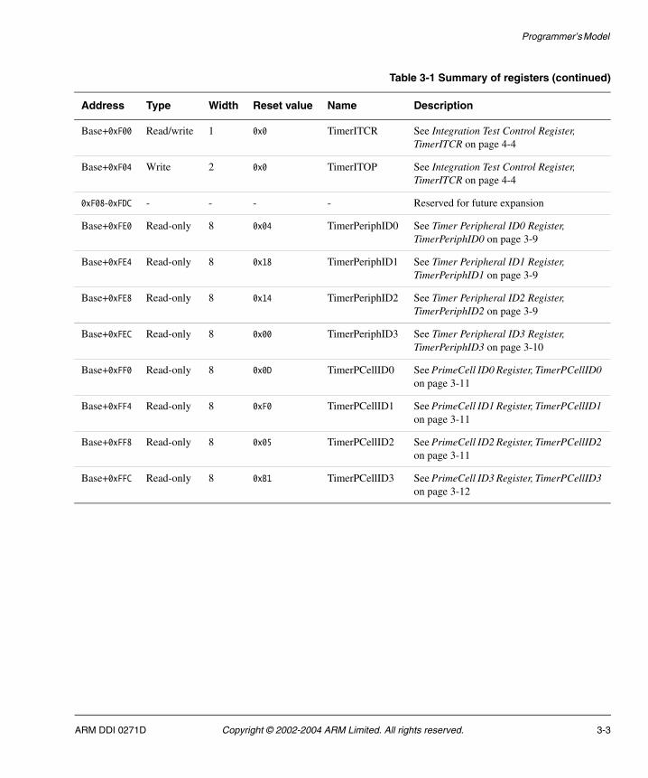
Base+0xF00 Read/write 1 0x0 TimerITCR See Integration Test Control Register, TimerITCR on page 4-4
Base+0xF04 Write 2 0x0 TimerITOP See Integration Test Control Register, TimerITCR on page 4-4
0xF08-0xFDC - - - - Reserved for future expansion
Base+0xFE0 Read-only 8 0x04 TimerPeriphID0 See Timer Peripheral ID0 Register, TimerPeriphID0 on page 3-9
Base+0xFE4 Read-only 8 0x18 TimerPeriphID1 See Timer Peripheral ID1 Register, TimerPeriphID1 on page 3-9
Base+0xFE8 Read-only 8 0x14 TimerPeriphID2 See Timer Peripheral ID2 Register, TimerPeriphID2 on page 3-9
Base+0xFEC Read-only 8 0x00 TimerPeriphID3 See Timer Peripheral ID3 Register, TimerPeriphID3 on page 3-10
Base+0xFF0 Read-only 8 0x0D TimerPCellID0 See PrimeCell ID0 Register, TimerPCellID0 on page 3-11
Base+0xFF4 Read-only 8 0xF0 TimerPCellID1 See PrimeCell ID1 Register, TimerPCellID1 on page 3-11
Base+0xFF8 Read-only 8 0x05 TimerPCellID2 See PrimeCell ID2 Register, TimerPCellID2 on page 3-11
Base+0xFFC Read-only 8 0xB1 TimerPCellID3 See PrimeCell ID3 Register, TimerPCellID3 on page 3-12
Table 3-1 Summary of registers (continued)
Address Type Width Reset value Name Description
ARM DDI 0271D Copyright © 2002-2004 ARM Limited. All rights reserved. 3-3

Programmer’s Model
3.2 Register descriptions
This section describes the dual Timer module registers:
• Load Register, TimerXLoad
• Current Value Register, TimerXValue on page 3-5
• Control Register, TimerXControl on page 3-5
• Interrupt Clear Register. TimerXIntClr on page 3-6
• Raw Interrupt Status Register, TimerXRIS on page 3-6
• Masked Interrupt Status Register, TimerXMIS on page 3-7
• Background Load Register, TimerXBGLoad on page 3-7
• Peripheral Identification Registers, TimerPeriphID0-3 on page 3-7
• PrimeCell Identification Registers, TimerPCellID0-3 on page 3-10.
Note The letter X used in register names means a register in either FRC1 or FRC2.
3.2.1 Load Register, TimerXLoad
The TimerXLoad Register is a 32-bit register that contains the value from which the counter is to decrement. This is the value used to reload the counter when Periodic mode is enabled, and the current count reaches zero.
When this register is written to directly, the current count immediately resets to the new value at the next rising edge of TIMCLK which is enabled by TIMCLKENX.
Note The minimum valid value for TimerXLoad is 1. If TimerXload is set to 0 then an interrupt is generated immediately.
The value in this register is also over-written if the TimerXBGLoad Register is written to, but the current count is not immediately affected.
If values are written to both the TimerXLoad and TimerXBGLoad Registers before an enabled rising edge on TIMCLK, then on the next enabled TIMCLK edge the value written to the TimerXLoad value replaces the current count value. After that, each time the counter reaches zero the current count value resets to the value written to TimerXBGLoad.
3-4 Copyright © 2002-2004 ARM Limited. All rights reserved. ARM DDI 0271D

Programmer’s Model
Reading from the TimerXLoad Register at any time after the two writes have occurred retrieves the value written to TimerXBGLoad. That is, the value read from TimerXLoad is always the value that takes effect for Periodic mode after the next time the counter reaches zero.
3.2.2 Current Value Register, TimerXValue
The TimerXValue Register is a 32-bit read-only register that gives the current value of the decrementing counter.
After a load operation has taken place by writing a new load value to TimerXLoad, the TimerXValue register reflects the new load value immediately in the PCLK clock domain without waiting for the next TIMCLK edge qualified by TIMCLKENX.
Note The most significant 16 bits of the 32-bit TimerXValue Register are not automatically set to 0 when in 16-bit timer mode. If the timer is in 16-bit mode then the most significant 16 bits of the TimerXValue Register might have a non-zero value if the timer was previously in 32-bit mode and a write to the TimerXLoad Register has not occurred since the change to 16-bit mode.
3.2.3 Control Register, TimerXControl
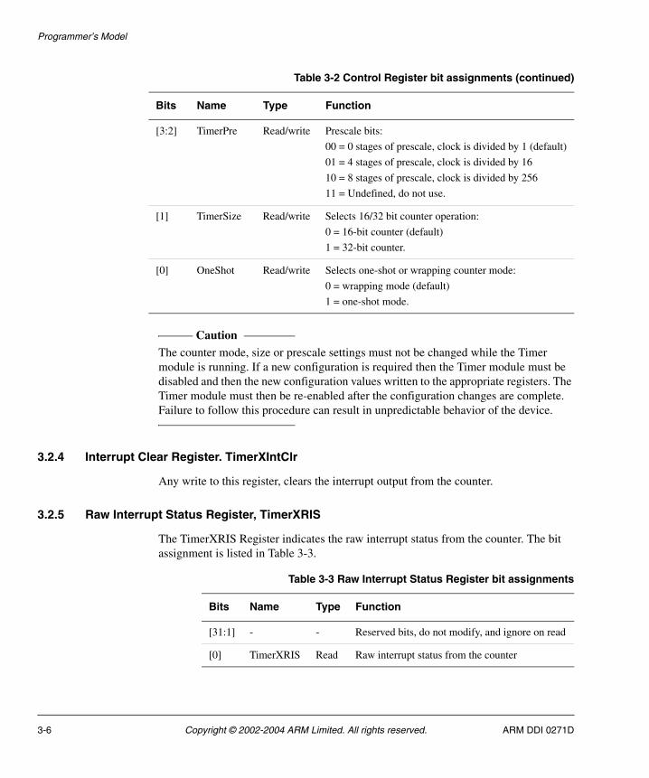
The bit assignments of the Control Register are listed in Table 3-2.
Table 3-2 Control Register bit assignments
Bits Name Type Function
[31:8] - - Reserved bits, do not modify, and ignore on read
[7] TimerEn Read/write Enable bit:
0 = Timer module disabled (default)
1 = Timer module enabled.
[6] TimerMode Read/write Mode bit:
0 = Timer module is in free-running mode (default)
1 = Timer module is in periodic mode.
[5] IntEnable Read/write Interrupt Enable bit:
0 = Timer module Interrupt disabled
1 = Timer module Interrupt enabled (default).
[4] - - Reserved bit, do not modify, and ignore on read
ARM DDI 0271D Copyright © 2002-2004 ARM Limited. All rights reserved. 3-5
Programmer’s Model
Caution The counter mode, size or prescale settings must not be changed while the Timer module is running. If a new configuration is required then the Timer module must be disabled and then the new configuration values written to the appropriate registers. The Timer module must then be re-enabled after the configuration changes are complete. Failure to follow this procedure can result in unpredictable behavior of the device.
3.2.4 Interrupt Clear Register. TimerXIntClr
Any write to this register, clears the interrupt output from the counter.
3.2.5 Raw Interrupt Status Register, TimerXRIS
The TimerXRIS Register indicates the raw interrupt status from the counter. The bit assignment is listed in Table 3-3.
[3:2] TimerPre Read/write Prescale bits:
00 = 0 stages of prescale, clock is divided by 1 (default)
01 = 4 stages of prescale, clock is divided by 16
10 = 8 stages of prescale, clock is divided by 256
11 = Undefined, do not use.
[1] TimerSize Read/write Selects 16/32 bit counter operation:
0 = 16-bit counter (default)
1 = 32-bit counter.
[0] OneShot Read/write Selects one-shot or wrapping counter mode:
0 = wrapping mode (default)
1 = one-shot mode.
Table 3-2 Control Register bit assignments (continued)
Bits Name Type Function
Table 3-3 Raw Interrupt Status Register bit assignments
Bits Name Type Function
[31:1] - - Reserved bits, do not modify, and ignore on read
[0] TimerXRIS Read Raw interrupt status from the counter
3-6 Copyright © 2002-2004 ARM Limited. All rights reserved. ARM DDI 0271D

Programmer’s Model
3.2.6 Masked Interrupt Status Register, TimerXMIS
The TimerXMIS Register indicates the masked interrupt status from the counter. This value is the logical AND of the raw interrupt status with the Timer Interrupt Enable bit from the control register, and is the same value which is passed to the interrupt output pin, TIMINTX. The bit assignment is listed in Table 3-4.
3.2.7 Background Load Register, TimerXBGLoad
The TimerXBGLoad Register is a 32-bit register that contains the value from which the counter is to decrement. This is the value used to reload the counter when Periodic mode is enabled, and the current count reaches zero.
This provides an alternative method of accessing the TimerXLoad Register. The difference is that writes to TimerXBGLoad do not cause the counter to restart from the new value immediately.
Reading from this register returns the same value returned from TimerXLoad. See Load Register, TimerXLoad on page 3-4 for more information.
3.2.8 Peripheral Identification Registers, TimerPeriphID0-3
The TimerPeriphID0-3 Registers are four 8-bit registers, that span address locations 0xFE0 - 0xFEC. The registers can conceptually be treated as a 32-bit register. The read-only registers provide the peripheral options listed in Table 3-5.
Figure 3-1 on page 3-8 shows the bit assignments for the registers.
Table 3-4 Masked Interrupt Status Register bit assignments
Bits Name Type Function
[31:1] - - Reserved bits, do not modify, and ignore on read
[0] TimerXMIS Read Enabled interrupt status from the counter
Table 3-5 Peripheral Identification Register options
Bits Function
PartNumber[11:0] This is used to identify the peripheral. The three digits product code 0x804 is used.
Designer ID[19:12] This is the identification of the designer. ARM Limited is 0x41 (ASCII A).
Revision[23:20] This is the revision number of the peripheral. The revision number starts from 0.
Configuration[31:24] This is the configuration option of the peripheral. The configuration value is 0.
ARM DDI 0271D Copyright © 2002-2004 ARM Limited. All rights reserved. 3-7

Programmer’s Model
Figure 3-1 Peripheral identification register bit assignment
Note When you design a system memory map you must remember that the peripheral has a 4KB-memory footprint. The 4-bit revision number is implemented by instantiating a component called RevAnd four times with its inputs tied off as appropriate, and the output sent to the read multiplexor. All memory accesses to the peripheral identification registers must be 32-bit, using the LDR instructions.
The four, 8-bit peripheral identification registers are described in the following subsections:
• Timer Peripheral ID0 Register, TimerPeriphID0 on page 3-9
• Timer Peripheral ID1 Register, TimerPeriphID1 on page 3-9
• Timer Peripheral ID2 Register, TimerPeriphID2 on page 3-9
• Timer Peripheral ID3 Register, TimerPeriphID3 on page 3-10.
31 24 23 20 19 16 15 12 11 8 7 0
Part number
Partnumber 1
Part number 0Designer 1 Designer 0
Designer
Revisionnumber
Configuration
7 00347034707
ConfigurationRevisionnumber
Conceptual registerbit assignment
Actual register bitassignment
3-8 Copyright © 2002-2004 ARM Limited. All rights reserved. ARM DDI 0271D

Programmer’s Model
Timer Peripheral ID0 Register, TimerPeriphID0
The TimerPeriphID0 Register is hard-coded and the fields in the register determine the reset value. Table 3-6 lists the bit assignments of the register.
Timer Peripheral ID1 Register, TimerPeriphID1
The TimerPeriphID1 Register is hard-coded and the fields in the register determine the reset value. Table 3-7 lists the bit assignments of the register.
Timer Peripheral ID2 Register, TimerPeriphID2
The TimerPeriphID2 register is hard-coded and the fields in the register determine the reset value. Table 3-8 lists the bit assignment of the register.
Table 3-6 Timer Peripheral ID0 Register bit assignments
Bit Name Description
[31:8] - Reserved, read undefined must be written as zeros
[7:0] PartNumber0 These bits read back as 0x04
Table 3-7 Timer Peripheral ID1 Register bit assignments
Bit Name Description
[31:8] - Reserved, read undefined, must be written as zeros
[7:4] Designer0 These bits read back as 0x1
[3:0] PartNumber1 These bits read back as 0x8
Table 3-8 Timer Peripheral ID2 Register bit assignments
Bit Name Description
[31:8] - Reserved, read undefined, must be written as zeros
[7:4] Revision These bits read back as 0x1
[3:0] Designer1 These bits read back as 0x4
ARM DDI 0271D Copyright © 2002-2004 ARM Limited. All rights reserved. 3-9

Programmer’s Model
Timer Peripheral ID3 Register, TimerPeriphID3
The TimerPeriphID3 register is hard-coded and the fields in the register determine the reset value. Table 3-9 shows the bit assignments of the register.
3.2.9 PrimeCell Identification Registers, TimerPCellID0-3
The TimerPCellID0-3 Registers are four 8-bit registers, that span address locations 0xFF0-0xFFC. The read-only registers can conceptually be treated as a 32-bit register. The register is used as a standard cross-peripheral identification system. The TimerPCellID Register is set to 0xB105F00D. Figure 3-2 shows the bit assignment for the registers.
Figure 3-2 PrimeCell identification register bit assignments
The four, 8-bit PrimeCell identification registers are described in the following subsections:
• PrimeCell ID0 Register, TimerPCellID0 on page 3-11
• PrimeCell ID1 Register, TimerPCellID1 on page 3-11
• PrimeCell ID2 Register, TimerPCellID2 on page 3-11
• PrimeCell ID3 Register, TimerPCellID3 on page 3-12.
Table 3-9 TimerPeriphID3 register bit assignments
Bit Name Description
[31:8] - Reserved, read undefined, must be written as zeros
[7:0] Configuration These bits read back as 0x00
31 24 23 16 15 8 7 0
TimerPCellID0
TimerPCellID0TimerPCellID1
TimerPCellID1
TimerPCellID2TimerPCellID3
7 0070707
TimerPCellID3 TimerPCellID2
Conceptual registerbit assignment
Actual register bitassignment
3-10 Copyright © 2002-2004 ARM Limited. All rights reserved. ARM DDI 0271D

Programmer’s Model
PrimeCell ID0 Register, TimerPCellID0
The TimerPCellID0 register is hard-coded and the fields in the register determine the reset value. Table 3-10 shows the bit assignments of the register.
PrimeCell ID1 Register, TimerPCellID1
The TimerPCellID1 register is hard-coded and the fields in the register determine the reset value. Table 3-11 shows the bit assignment of the register.
PrimeCell ID2 Register, TimerPCellID2
The TimerPCellID2 register is hard-coded and the fields in the register determine the reset value. Table 3-12 shows the bit assignment of the TimerPCellID2 register.
Table 3-10 PrimeCell ID0 Register bit assignments
Bit Name Description
[31:8] - Reserved, read undefined, must be written as zeros
[7:0] TimerPCellID0 These bits read back as 0x0D
Table 3-11 PrimeCell ID1 Register bit assignments
Bit Name Description
[31:8] - Reserved, read undefined, must be written as zeros
[7:0] TimerPCellID1 These bits read back as 0xF0
Table 3-12 PrimeCell ID2 Register bit assignments
Bit Name Description
[31:8] - Reserved, read undefined, must be written as zeros
[7:0] TimerPCellID2 These bits read back as 0x05
ARM DDI 0271D Copyright © 2002-2004 ARM Limited. All rights reserved. 3-11

Programmer’s Model
PrimeCell ID3 Register, TimerPCellID3
The TimerPCellID3 register is hard-coded and the fields in the register determine the reset value. Table 3-13 shows the bit assignment of the TimerPCellID3 register.
Table 3-13 PrimeCell ID3 Register bit assignments
Bit Name Description
[31:8] - Reserved, read undefined, must be written as zeros
[7:0] TimerPCellID3 These bits read back as 0xB1
3-12 Copyright © 2002-2004 ARM Limited. All rights reserved. ARM DDI 0271D

Chapter 4 Programmer’s Model for Test
This chapter describes the additional logic for functional verification and production testing. It contains the following sections:
• Integration test harness overview on page 4-2
• Scan testing on page 4-3
• Test registers on page 4-4.
ARM DDI 0271D Copyright © 2002-2004 ARM Limited. All rights reserved. 4-1

Programmer’s Model for Test
4.1 Integration test harness overview
The Dual-Timer module contains an integration test harness to enable the direct control of the non-AMBA module outputs for test purposes. The test harness is controlled by Integration Test Registers, TIMERITCR and TIMERITOP. This enables the connectivity of the TIMINT1, TIMINT2, and TIMINTC output signals to other modules in a SoC device to be easily verified using only transfers from the APB bus.
Figure 3-1 shows a block diagram of the output integration test harness and how TIMINT1, TIMINT2, and TIMINTC are controlled in integration test mode.
Figure 4-1 Output integration test harness
Timer module
outputs
TimerITOP
Register0
1TimerITOP[1]
TimerITOP[0]
0
1
Internal TIMINT1 signal
Internal TIMINT2 signal
TimerITCR
RegisterITEN
TIMINT2
TIMINT1
TIMINTC
From
Timer core
4-2 Copyright © 2002-2004 ARM Limited. All rights reserved. ARM DDI 0271D
Programmer’s Model for Test
4.2 Scan testing
The Dual-Timer module has been designed to simplify:
• insertion of scan test cells
• use of Automatic Test Pattern Generation (ATPG).
This is the recommended method of manufacturing test.
The Dual-Timer module includes placeholder signals to aid the scan insertion process. These are:
• SCANENABLE• SCANINPCLK• SCANOUTPCLK.
ARM DDI 0271D Copyright © 2002-2004 ARM Limited. All rights reserved. 4-3
Programmer’s Model for Test
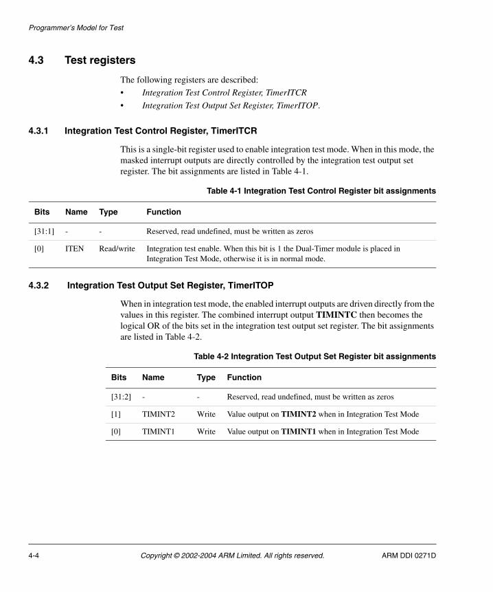
4.3 Test registers
The following registers are described:
• Integration Test Control Register, TimerITCR
• Integration Test Output Set Register, TimerITOP.
4.3.1 Integration Test Control Register, TimerITCR
This is a single-bit register used to enable integration test mode. When in this mode, the masked interrupt outputs are directly controlled by the integration test output set register. The bit assignments are listed in Table 4-1.
4.3.2 Integration Test Output Set Register, TimerITOP
When in integration test mode, the enabled interrupt outputs are driven directly from the values in this register. The combined interrupt output TIMINTC then becomes the logical OR of the bits set in the integration test output set register. The bit assignments are listed in Table 4-2.
Table 4-1 Integration Test Control Register bit assignments
Bits Name Type Function
[31:1] - - Reserved, read undefined, must be written as zeros
[0] ITEN Read/write Integration test enable. When this bit is 1 the Dual-Timer module is placed in Integration Test Mode, otherwise it is in normal mode.
Table 4-2 Integration Test Output Set Register bit assignments
Bits Name Type Function
[31:2] - - Reserved, read undefined, must be written as zeros
[1] TIMINT2 Write Value output on TIMINT2 when in Integration Test Mode
[0] TIMINT1 Write Value output on TIMINT1 when in Integration Test Mode
4-4 Copyright © 2002-2004 ARM Limited. All rights reserved. ARM DDI 0271D

Appendix A Signal Descriptions
This chapter describes the signals that interface with the Dual-Timer Module (SP804). It contains the following sections:
• AMBA APB signals on page A-2
• Non-AMBA signals on page A-3.
ARM DDI 0271D Copyright © 2002-2004 ARM Limited. All rights reserved. A-1

Signal Descriptions
A.1 AMBA APB signals
The Dual-Timer module is connected to the AMBA APB as a bus slave. Table A-1 describes the APB interface signals.
Table A-1 AMBA APB signal descriptions
Name Type Source/Destination Description
PADDR[11:2] Input APB bridge Subset of the AMBA APB address bus.
PCLK Input Clock generator AMBA APB clock.
PENABLE Input APB bridge AMBA APB enable signal. PENABLE is asserted HIGH for one cycle of PCLK to enable a bus transfer.
PRDATA[31:0] Output APB bridge Unidirectional AMBA APB read data bus.
PRESETn Input Reset controller APB bus reset signal, active LOW.
PSEL Input APB bridge Timer module select signal from the decoder within the APB bridge. When HIGH this signal indicates the slave device is selected by the APB bridge, and that a data transfer is required.
PWDATA[31:0] Input APB bridge Unidirectional AMBA APB write data bus.
PWRITE Input APB bridge AMBA APB transfer direction signal, indicates a write access when HIGH, read access when LOW.
A-2 Copyright © 2002-2004 ARM Limited. All rights reserved. ARM DDI 0271D

Signal Descriptions
A.2 Non-AMBA signals
Table A-2 describes the Dual-Timer module non-AMBA signals.
Table A-2 Non-AMBA signals
Name Type Source/Destination Description
TIMCLK Input Clock generator Timer clock
TIMCLKEN1 Input Clock generator Timer1 clock enable
TIMCLKEN2 Input Clock generator Timer2 clock enable
TIMINT1 Output Interrupt controller Timer1 interrupt, active HIGH
TIMINT2 Output Interrupt controller Timer2 interrupt, active HIGH
TIMINTC Output Interrupt controller Combined interrupt, active HIGH
SCANENABLE Input Test controller Placeholder for Dual-Timer module scan enable signal
SCANINPCLK Input Test controller Placeholder for Dual-Timer module input scan signal
SCANOUTPCLK Output Test controller Placeholder Dual-Timer module output scan signal
ARM DDI 0271D Copyright © 2002-2004 ARM Limited. All rights reserved. A-3

Signal Descriptions
A-4 Copyright © 2002-2004 ARM Limited. All rights reserved. ARM DDI 0271D
Index
AAbout the module 1-2AMBA 1-3APB 2-5APB signals A-2
BBackground Load Register 3-7
CClock
enable 2-6signals 2-6
Control Register 3-5Conventions
numerical xiiregister fields xiisignal xi
word length xiiCurrent Value Register 3-5
FFRC 2-2Free running counter 2-2, 2-5Functional description 2-4Functional overview 2-2
IIdentification Registers 1-3, 2-14, 3-7,
3-10Integration Test Control Register 4-4Integration test harness 4-2Integration Test Output Set Register
4-4Interface reset 2-5Interrupt 1-3
behavior 2-11
generation 1-4masking 1-4
Interrupt Clear Register 3-6Interrupt Status Register 3-7
LLoad Register 3-4
MMode 1-4
free-running 2-2, 2-9one-shot 2-2, 2-11periodic 2-2, 2-10
NNon-AMBA signals A-3Numerical conventions xii
ARM DDI 0271D Copyright © 2002-2004 ARM Limited. All rights reserved. Index-1
Index
PPeripheral Identification Registers 3-7Prescaler 1-4
operation 2-8PrimeCell Identification Registers
3-10Product revision status xProgrammable parameters 1-4
RRaw Interrupt Status Register 3-6Register descriptions 3-4
Background Load Register 3-7Control Register 3-5Current Value Register 3-5Interrupt Clear Register 3-6Load Register 3-4Masked Interrupt Status Register
3-7Peripheral Identification Registers
3-7PrimeCell Identification Registers
3-10Raw Interrupt Status Register 3-6
Register field conventions xiiReset signal 2-5Revision status x
SScan testing 4-3Signal conventions xiSignals
APB A-2non-AMBA A-3
Summary of registers 3-2
TTest registers
Integration Test Control Register 4-4
Integration Test Output Set Register 4-4
Timer intervalprogramming 2-12
TimerITCR 4-4TimerITOP 4-4TimerPCellID0-3 3-10TimerPeriphID0-3 3-7TimerXBGLoad 3-7TimerXControl 3-5TimerXIntClr 3-6TimerXLoad 3-4TimerXMIS 3-7TimerXRIS 3-6TimerXValue 3-5
WWord length conventions xii
Index-2 Copyright © 2002-2004 ARM Limited. All rights reserved. ARM DDI 0271D


