ARM Cortex board - Asian Institute of Technologyesl.ait.ac.th/courses/AT74.08/class5.pdf · •In...
48
1 ARM Cortex board
-
Upload
trinhtuong -
Category
Documents
-
view
215 -
download
1
Transcript of ARM Cortex board - Asian Institute of Technologyesl.ait.ac.th/courses/AT74.08/class5.pdf · •In...
1
ARM Cortex board
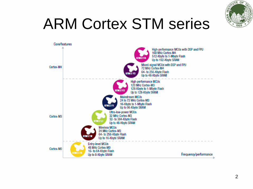
2
ARM Cortex STM series

STM32 Series
3

Abbreviation • FS full speed
• HS high speed
• MC motor controller
• MSI multi speed internal oscillator
• RNG random number generator
• SDIO secure digital input output
• VScal voltage scaling
• DSC digital signal controller
• PGA programmable gain ampilier 4
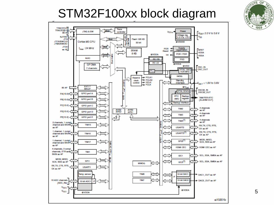
STM32F100xx block diagram
5
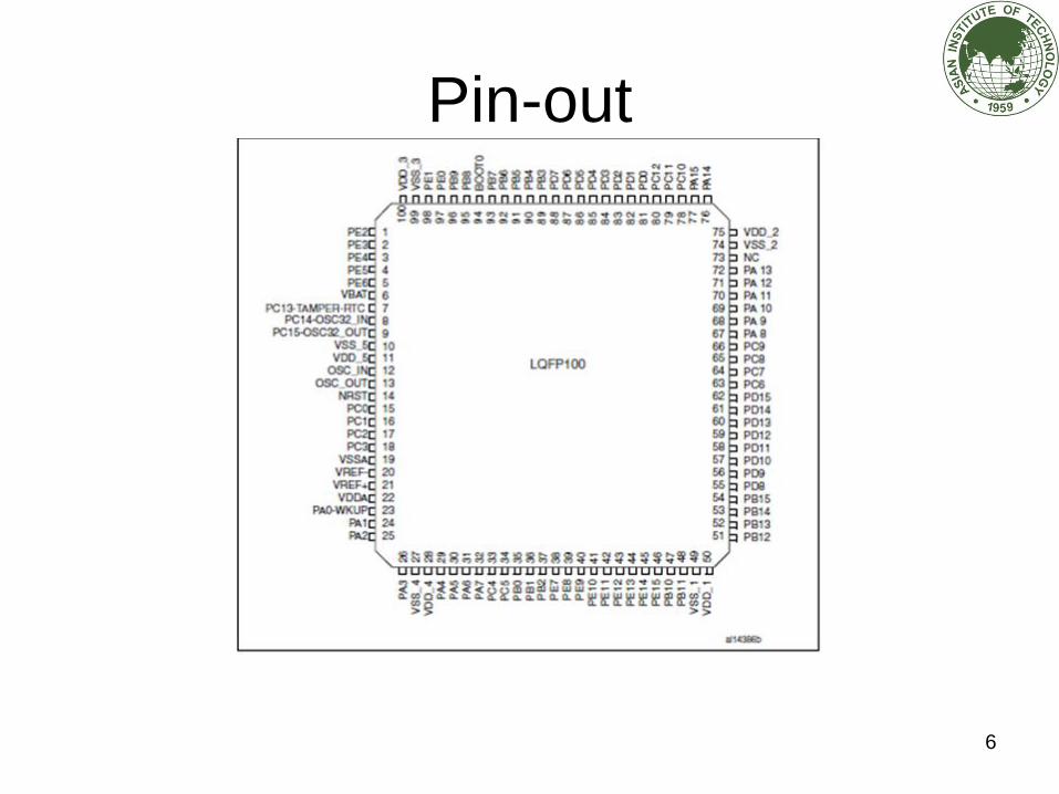
Pin-out
6
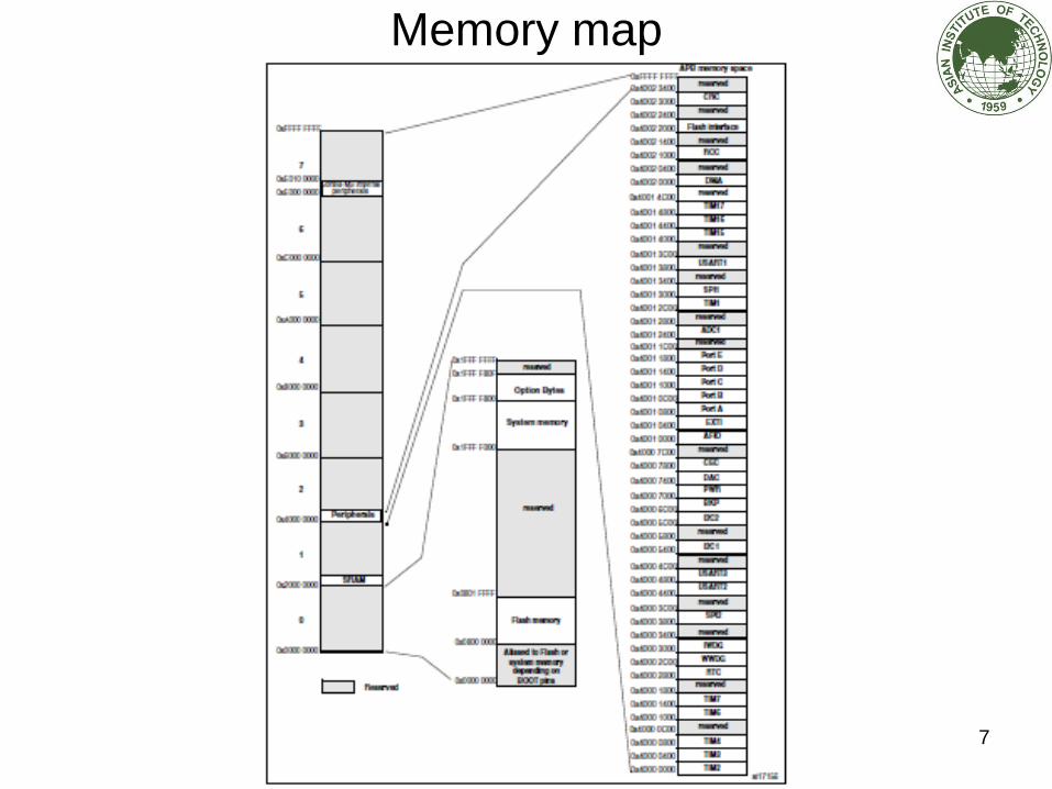
Memory map
7

Memory map (1)
8

Memory map (2)
9

Memory map(3)
10

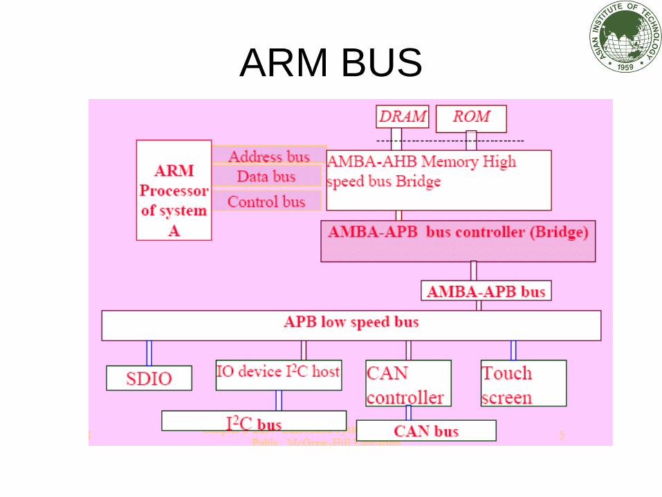
ARM Bus
• Introduced by ARM Ltd in 1996
• Widely used as the on-chip bus

ARM BUS
• AMBA = ARM Memory Bus Architecture
• AHB = ARM High performance Bus
• APB = ARM Peripheral Bus
• AMBA-AHB connects ARM core with
memory, external DRAM
• AMBA-APB interfaces ARM core with
external low-speed I/O devices using
AMBA-APB bridge
AMBA
• AMBA-AHB connects to 32-bit data and
32-bit address at high speed
• AHB maximum bps bandwidth is 16 times
ARM processor clock
• AMBA-APB bridge is used to
communicate AHB bus to APB bus
• The bridge communicates to memory
through AMBA-AHB

AHB Bus
• AHB Bus are interconnected with:
– Cortex core
– Internal SRAM
– Internal Flash memory
– FSMC
– AHB to APB
– DMA
– Ethernet DMA
14
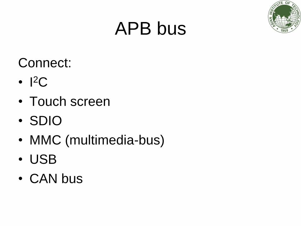
APB bus
Connect:
• I2C
• Touch screen
• SDIO
• MMC (multimedia-bus)
• USB
• CAN bus
ARM BUS

System architecture
17
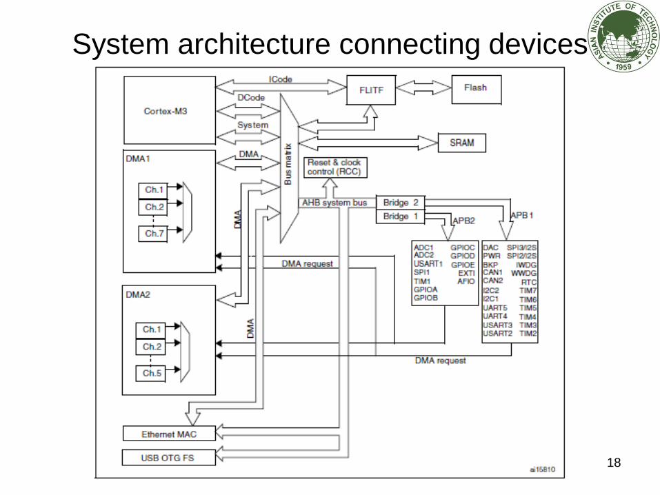
System architecture connecting devices
18

Bus system
• Icode bus : connects the instruction bus to the flash
memory instruction interface
• Dcode bus : connects to flash memory data interface
and debug access
• System bus : connects to bus matrix that manages the
arbitration between core and DMA
• DMA bus: AHB master interface of the DMA to bus
matrix
• Bus matrix: arbitrations between different buses
• AHB/APB bridge: bridge between AHB and APB
APB1 is limited at 36 MHz and APB2 is at 72 MHz
19
AHB and APB
• AHB = Advance High Performance Bus with
max speed = 72 Mhz
• APB = Advance Peripheral Bus with APB1 max
speed = 36 Mhz and APB2 max speed = 72
MHz
• FSMC = Flexible static memory controller (able
to interface with synchronous and
asynchronous)
20
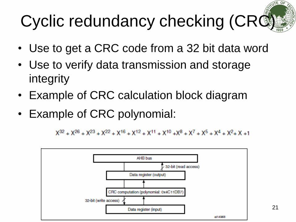
Cyclic redundancy checking (CRC)
• Use to get a CRC code from a 32 bit data word
• Use to verify data transmission and storage
integrity
• Example of CRC calculation block diagram
• Example of CRC polynomial:
21
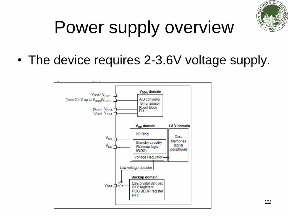
Power supply overview
• The device requires 2-3.6V voltage supply.
22
Power supply
• Voltage regulator to provide 1.8V for core
and memory
• Reset and Clock control, real time clock,
and LSE (Low speed external crystal)
oscillator are supported by backup domain
power source
23
Low power mode
• Normal condition: run mode
• Low power mode:
– Sleep mode
CPU clocks are off, all peripherals are running
– Stop mode
all clocks are off
– Standby mode
1.8 V power domain are off (enter backup domain)
24

Low power mode
WFI (wait for interrupt) and WFE (wait for
event) are special ARM instructions 25
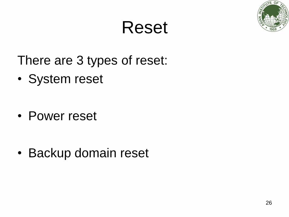
Reset
There are 3 types of reset:
• System reset
• Power reset
• Backup domain reset
26
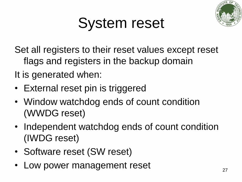
System reset
Set all registers to their reset values except reset
flags and registers in the backup domain
It is generated when:
• External reset pin is triggered
• Window watchdog ends of count condition
(WWDG reset)
• Independent watchdog ends of count condition
(IWDG reset)
• Software reset (SW reset)
• Low power management reset
27

Power reset
Set all registers to their reset values except
registers in the backup domain
It is generated when:
• Power on/ Power down reset
• When exiting standby mode
28

Backup domain reset
Effects only the backup domain
It is generated when:
• Software reset
• VDD or VBAT, if both supplies have previously
been off
29

STM32F10xxx board
30

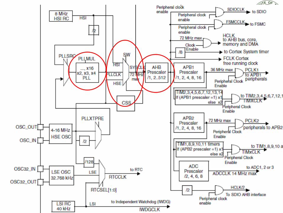
Clocks Three different clock sources can be used to drive
SYSCLK
• HSI (High speed Internal) oscillator clock
• HSE (High speed External) oscillator clock
• PLL clock
The devices have two secondary clock sources
• 40 kHz low speed internal (LSI) RC for the
independent watchdog and optionally drive RTC
• 32.768 KHz low speed external crystal (LSE) which
optionally drive RTC
Each clock source can be switched on/off independently 31
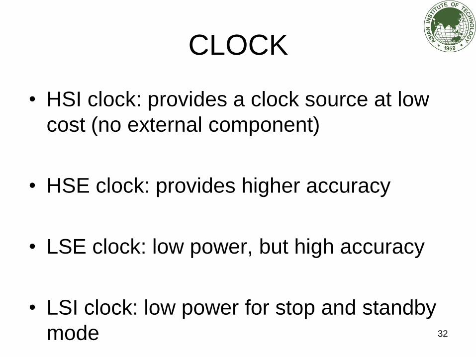
CLOCK
• HSI clock: provides a clock source at low
cost (no external component)
• HSE clock: provides higher accuracy
• LSE clock: low power, but high accuracy
• LSI clock: low power for stop and standby
mode
32
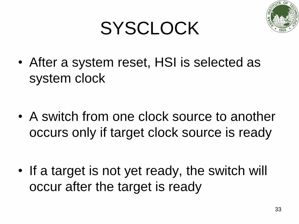
SYSCLOCK
• After a system reset, HSI is selected as
system clock
• A switch from one clock source to another
occurs only if target clock source is ready
• If a target is not yet ready, the switch will
occur after the target is ready
33

Clock tree
34
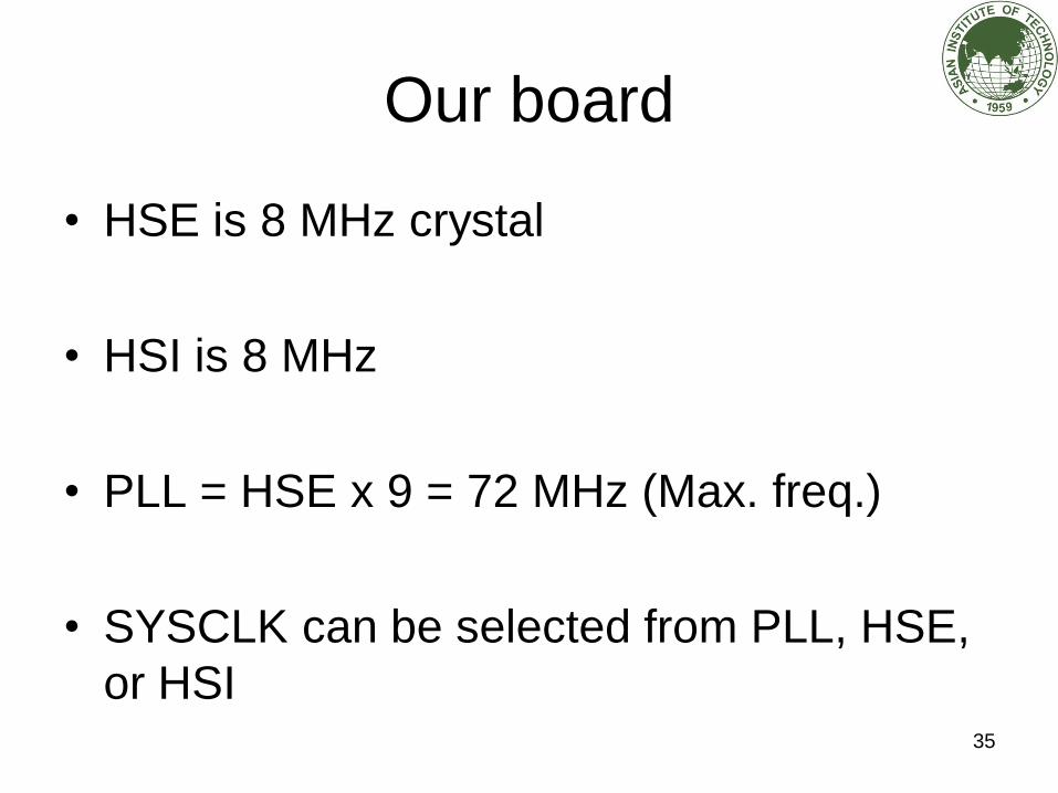
Our board
• HSE is 8 MHz crystal
• HSI is 8 MHz
• PLL = HSE x 9 = 72 MHz (Max. freq.)
• SYSCLK can be selected from PLL, HSE,
or HSI 35
36

Real Time Clock (RTC)
• RTC can be either HSE/128, LSE or LSI
clock which is set by the backup domain
control register
• If LSE is selected, RTC continues to work
even if VDD is powered off, provided that
VBAT is maintained
37
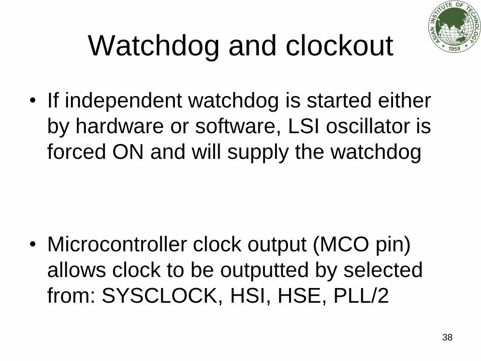
Watchdog and clockout
• If independent watchdog is started either
by hardware or software, LSI oscillator is
forced ON and will supply the watchdog
• Microcontroller clock output (MCO pin)
allows clock to be outputted by selected
from: SYSCLOCK, HSI, HSE, PLL/2
38

Output clock
• HCLK : for AHB bus, core, memory and DMA
• FCLK: free running clock
• PCLK1: to APB1
• PCLK2: to APB2
• TIM1CLK: Timer 1
• TIMxCLK: Timer 2,3,4
• ADCCLK: to ADC module
39

Reset and Clock Control (RCC)
• RCC is a set of register to setup for reset
and clock control
40
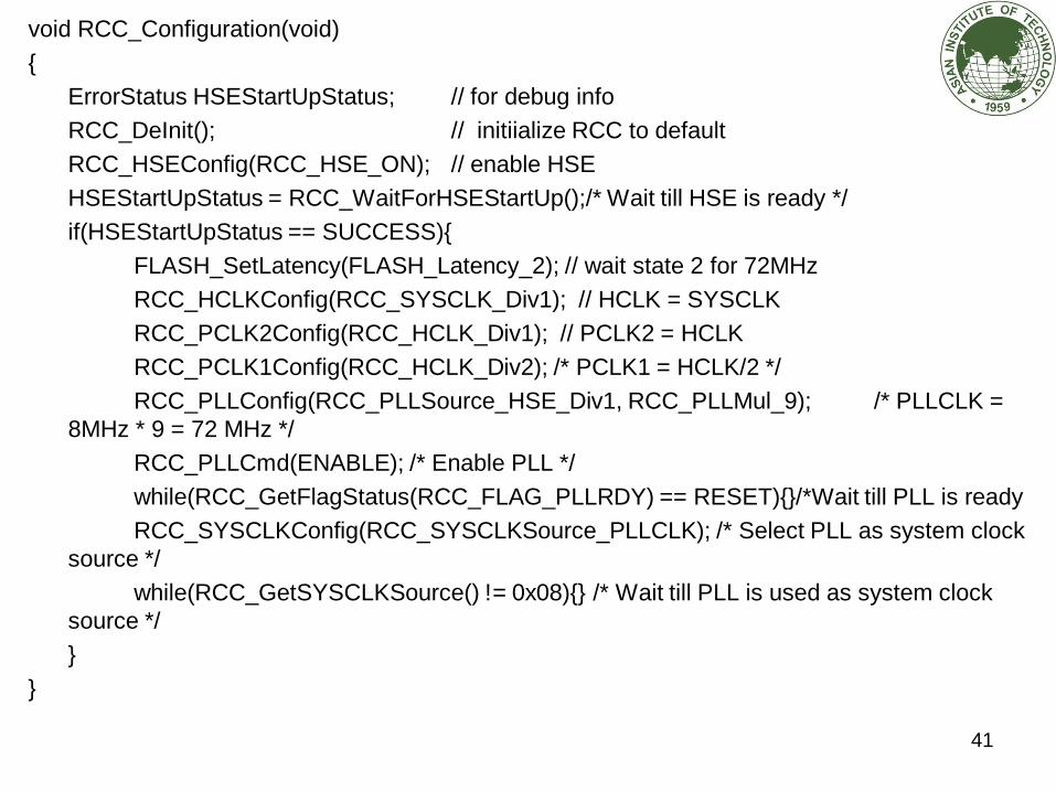
void RCC_Configuration(void)
{
ErrorStatus HSEStartUpStatus; // for debug info
RCC_DeInit(); // initiialize RCC to default
RCC_HSEConfig(RCC_HSE_ON); // enable HSE
HSEStartUpStatus = RCC_WaitForHSEStartUp();/* Wait till HSE is ready */
if(HSEStartUpStatus == SUCCESS){
FLASH_SetLatency(FLASH_Latency_2); // wait state 2 for 72MHz
RCC_HCLKConfig(RCC_SYSCLK_Div1); // HCLK = SYSCLK
RCC_PCLK2Config(RCC_HCLK_Div1); // PCLK2 = HCLK
RCC_PCLK1Config(RCC_HCLK_Div2); /* PCLK1 = HCLK/2 */
RCC_PLLConfig(RCC_PLLSource_HSE_Div1, RCC_PLLMul_9); /* PLLCLK =
8MHz * 9 = 72 MHz */
RCC_PLLCmd(ENABLE); /* Enable PLL */
while(RCC_GetFlagStatus(RCC_FLAG_PLLRDY) == RESET){}/*Wait till PLL is ready
RCC_SYSCLKConfig(RCC_SYSCLKSource_PLLCLK); /* Select PLL as system clock
source */
while(RCC_GetSYSCLKSource() != 0x08){} /* Wait till PLL is used as system clock
source */
}
}
41
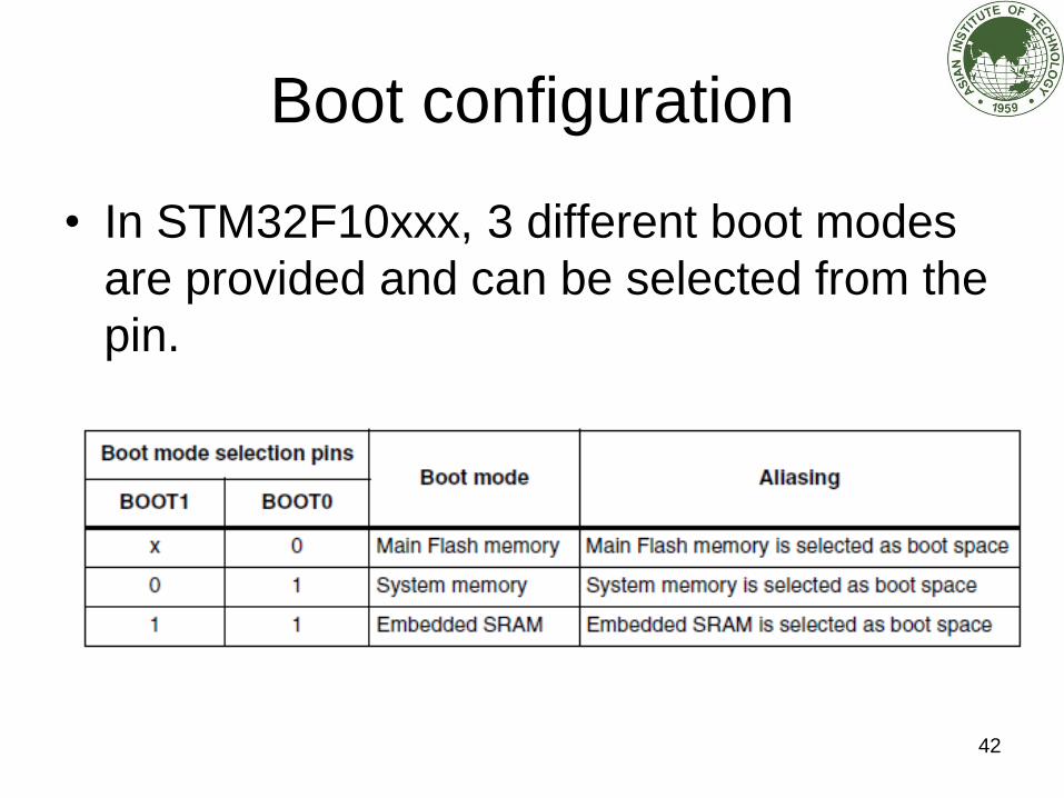
Boot configuration
• In STM32F10xxx, 3 different boot modes
are provided and can be selected from the
pin.
42
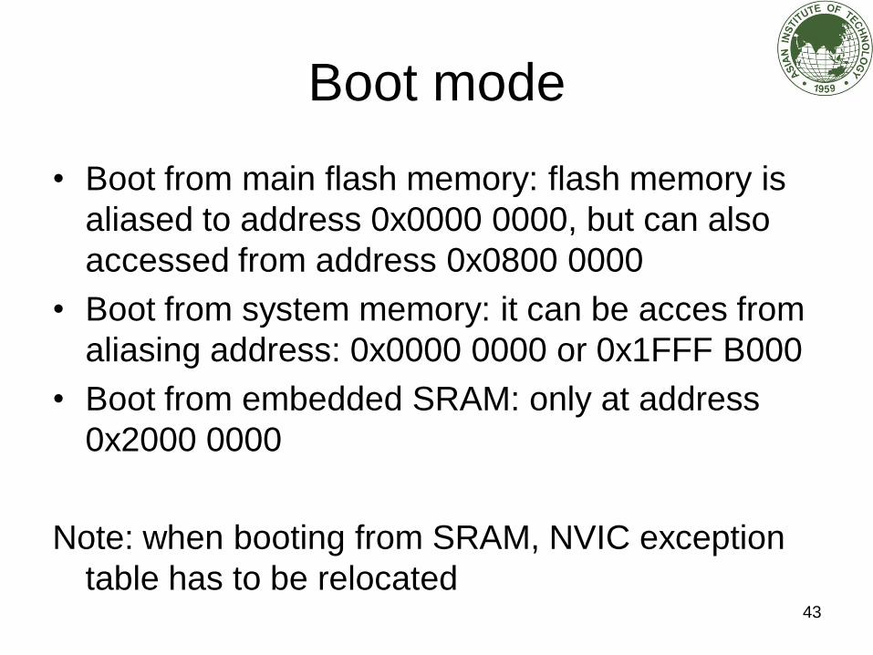
Boot mode
• Boot from main flash memory: flash memory is
aliased to address 0x0000 0000, but can also
accessed from address 0x0800 0000
• Boot from system memory: it can be acces from
aliasing address: 0x0000 0000 or 0x1FFF B000
• Boot from embedded SRAM: only at address
0x2000 0000
Note: when booting from SRAM, NVIC exception
table has to be relocated 43
Bit banding
• Bit band operation support allows a single
load/store operation to access a single
data bit
• In ARM Cortex M3, this is supported in two
predefined memory regions call bit-band
regions
• One of them is located in the first 1 MB of
the SRAM and the other is located in the
first 1 MB of the peripheral region
44

Bit-band region
45
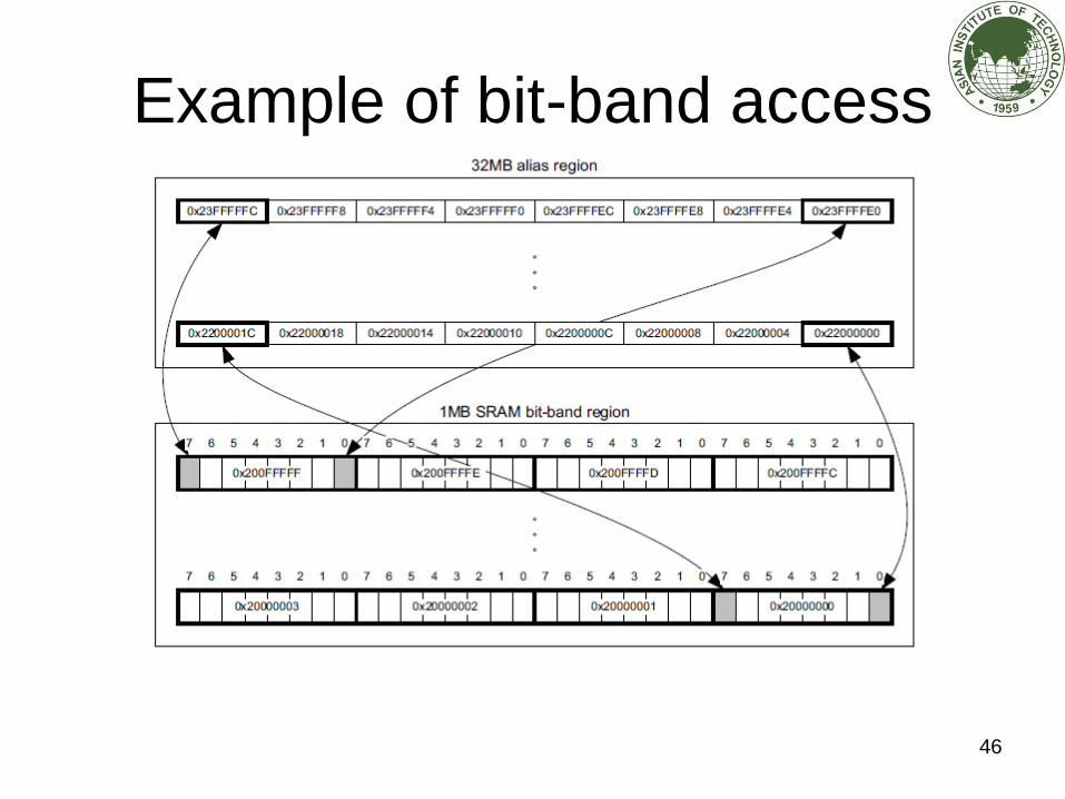
Example of bit-band access
46
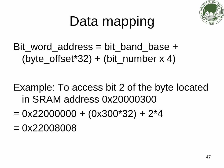
Data mapping
Bit_word_address = bit_band_base +
(byte_offset*32) + (bit_number x 4)
Example: To access bit 2 of the byte located
in SRAM address 0x20000300
= 0x22000000 + (0x300*32) + 2*4
= 0x22008008
47

Questions?
48