Area, Power, Delay Performance Analysis of Logic Element Using Various · PDF...
9
International Journal of Engineering Science Invention Volume 2 Issue 3 ǁ March. 2013 Area, Power, Delay Performance Analysis of Logic Element Using Various Architecture Shilpa.B 1 , Udaiya kumar.R 2 , Sankaranarayan.K 3 Department of ECE 1 ,Associate Professor and Head of ECE 2 , ECET 3 ABSTRACT: Field Programmable Gate Arrays (FPGA’s) are consider as power hungry device and not preferred as portable devices due to this disadvantage, hence the power reduction on Logic Element will make FPGA suitable for portable devices. Recently many techniques have been proposed for power reduction in conventional Logic Element (LE's) in reconfigurable computing devices such as FPGA's. The conventional logic element used in FPGA's is the flip flops. The conventional logic element in FPGA's consists of LUT (Look-Up Table), storage element as D-flip-flop and Multiplexer (MUX).The Output of LUT is connected to input of Multiplexer and storage element and the clock of flip flop is always connected to clock signal. Understanding the suitability of flip-flops, multiplexer and selecting the best topology for a given application is an important issue to fulfill the need of the design to satisfy low power and high performance circuit. This paper presents a widespread comparison in terms of its area, transistor count, delay values and power dissipation. In this paper, we describe the analysis for 16x1 multiplexer, D-flip-flop's for area, power dissipation and a propagation delay at 16nm technology is carried out in TANNER SPICE TOOL V 13.0. Hence to optimize the Static & Dynamic power in Logic Element of FPGA using 16nm, BSIM-4, Predictive Technology Modeling (PTM) and to study the impacts. Keywords: FPGA’s, LE's, LUT, BSIM, PTM, ASIC I. INTRODUCTION A field-programmable gate array (FPGA) is integrated circuit designed to be configured by the customer or designer after manufacturing. The FPGA configuration is generally specified using Hardware descriptive language (HDL), similar to that used for an Application specific integrated circuit (ASIC).FPGAs can be used to implement any logical function that an ASIC could perform. FPGAs contain programmable logic components called "logic blocks", and a hierarchy of reconfigurable interconnects that allow the blocks to be "wired together".While Multiplexers are primarily thought of as “data selectors” because they select one of several inputs to be logically connected to the output, they can also be used to implement Boolean functions.A multiplexer consists of n inputs, m-bit select word to connect one of the inputs to the output. To cover every input, we choose m such that m= log 2 (n) where m is the number of select lines. A flip- flop is a bistable circuit which stores a logic state of 0 or 1 in response to a clock pulse with one or more data inputs. In digital circuit design, large proportion contributes to synchronous design and they are operated based on the clock signal to reduce the complexity of the circuit design. In the design of sequential circuits, a major challenge is the design of an efficient D flip-flop (DFF). Several static/dynamic DFF architectures have been proposed [5],[6],[8],[10]and[14].The explanation towards True-Single-Phase Clocking (TSPC) proposed in [11] is an efficient methodology to achieve very high-speed VLSI design. TSPC is safer and takes less clock signal routing area. II. FPGA ARCHITECTURE & POWER DISSIPATION: FPGA Architecture: The most common FPGA architecture (Fig.1) consists of an array of logic blocks (called Configurable Logic Block, CLB, or Logic Array Block, LAB, depending on vendor), I/O pads, and routing channels. Generally, all the routing channels have the same width (number of wires). Multiple I/O pads may fit into the height of one row or the width of one column in the array A logic block generally termed as configurable logic block or logic array block (CLB or LAB) consists of a few logical cells (called ALM, LE, Slice etc.).
Transcript of Area, Power, Delay Performance Analysis of Logic Element Using Various · PDF...

International Journal of Engineering Science Invention
Volume 2 Issue 3 ǁ March. 2013
Area, Power, Delay Performance Analysis of Logic Element Using
Various Architecture
Shilpa.B1, Udaiya kumar.R
2, Sankaranarayan.K
3
Department of ECE1,Associate Professor and Head of ECE2, ECET3
ABSTRACT: Field Programmable Gate Arrays (FPGA’s) are consider as power hungry device and not preferred as portable devices due to this disadvantage, hence the power reduction on Logic Element will make FPGA suitable for portable devices. Recently many techniques have been proposed for power reduction in conventional Logic Element (LE's) in reconfigurable computing devices such as FPGA's. The conventional logic element used in FPGA's is the flip flops. The conventional logic element in FPGA's consists of LUT (Look-Up Table), storage element as D-flip-flop and Multiplexer (MUX).The Output of LUT is connected to input of Multiplexer and storage element and the clock of flip flop is always connected to clock signal. Understanding the suitability of flip-flops, multiplexer and selecting the best topology for a given application is an important issue to fulfill the need of the design to satisfy low power and high performance circuit. This paper presents a widespread comparison in terms of its area, transistor count, delay values and power dissipation. In this paper, we describe the analysis for 16x1 multiplexer, D-flip-flop's for area, power dissipation and a propagation delay at 16nm technology is carried out in TANNER SPICE TOOL V 13.0. Hence to optimize the Static & Dynamic power in Logic Element of FPGA using 16nm, BSIM-4, Predictive Technology Modeling (PTM) and to study the impacts.
Keywords: FPGA’s, LE's, LUT, BSIM, PTM, ASIC
I. INTRODUCTION A field-programmable gate array (FPGA) is integrated circuit designed to be configured by the
customer or designer after manufacturing. The FPGA configuration is generally specified using Hardware
descriptive language (HDL), similar to that used for an Application specific integrated circuit (ASIC).FPGAs
can be used to implement any logical function that an ASIC could perform. FPGAs contain programmable logic
components called "logic blocks", and a hierarchy of reconfigurable interconnects that allow the blocks to be
"wired together".While Multiplexers are primarily thought of as “data selectors” because they select one of
several inputs to be logically connected to the output, they can also be used to implement Boolean functions.A
multiplexer consists of n inputs, m-bit select word to connect one of the inputs to the output.
To cover every input, we choose m such that m= log2 (n) where m is the number of select lines. A flip-
flop is a bistable circuit which stores a logic state of 0 or 1 in response to a clock pulse with one or more data
inputs. In digital circuit design, large proportion contributes to synchronous design and they are operated based
on the clock signal to reduce the complexity of the circuit design. In the design of sequential circuits, a major
challenge is the design of an efficient D flip-flop (DFF). Several static/dynamic DFF architectures have been
proposed [5],[6],[8],[10]and[14].The explanation towards True-Single-Phase Clocking (TSPC) proposed in [11]
is an efficient methodology to achieve very high-speed VLSI design. TSPC is safer and takes less clock signal
routing area.
II. FPGA ARCHITECTURE & POWER DISSIPATION: FPGA Architecture:
The most common FPGA architecture (Fig.1) consists of an array of logic blocks (called Configurable
Logic Block, CLB, or Logic Array Block, LAB, depending on vendor), I/O pads, and routing channels.
Generally, all the routing channels have the same width (number of wires). Multiple I/O pads may fit into the
height of one row or the width of one column in the array A logic block generally termed as configurable logic
block or logic array block (CLB or LAB) consists of a few logical cells (called ALM, LE, Slice etc.).

AREA, POWER, DELAY PERFORMANCE ANALYSIS
Figure 1: FPGA Architecture
III. POWER DISSIPATION: Power dissipation is the rate at which the energy is taking from the source and converted into heat. The
total power dissipation is given by
P total = Pstatic +P dynamic (1)
i. Dynamic power dissipation: Dynamic power dissipation is caused by transient switching from one state to another, Short circuit
power dissipation. In submicron technology dynamic power consumption contributes significantly to overall
power consumption. Every time a capacitive node switches from ground to Supply, energy of CLVDD² is
consumed. It depends on the switching activity of the signal. Signals in CMOS devices transit back and forth
between two logic levels resulting in the charging and discharging of parasitic capacitance. This is the
dominant factor of power dissipation (transient switching). For a small instant of time both PMOS and NMOS
will be “on” simultaneously. The duration depends on the input and output transition (rise and fall times). So a
direct path exists between VDD and GND (short circuit). The dynamic power consumption is given by
PDYN=1
2CLVDD
2fc (2)
Where
CL = load capacitance
VDD = supply voltage
fc = clock frequency
These parameters are not completely orthogonal and cannot be optimized independently.
ii. Static power dissipation: This is caused mainly due to leakage current. When a CMOS integrated circuit is not switching, there
should be no DC current paths from VCC to ground and the device should not draw any supply current at all.
However, due to the inherent nature of semiconductors, a small amount of leakage current flows across all
reverse-biased junctions on the integrated circuit. These leakages are caused by thermally-generated charge
carriers in the diode area. As the temperature of the diode increases, so do the number of these unwanted charge
carriers also increases. Leakage currents are mainly due to reduction in Threshold voltage, Channel length and
Oxide thickness. Threshold voltage scaling results in substantial increase of sub threshold leakage current.
Oxide thickness has to be reduced in proportion to the channel length. Oxide thickness reduction results in
increase in the electric field.

AREA, POWER, DELAY PERFORMANCE ANALYSIS
iii. Power Hungry Parts in FPGA
The power hungry parts in FPGA are Logic Block, Routing Channel, Input/output pads. One logic
block is a cluster of lookup tables (LUTs) with the cluster size N (i.e., the number of LUTs inside one cluster)
and the LUT size k (i.e., the number of inputs to the LUT) as the architectural parameters. Logic blocks are
embedded into the routing resources as logic “islands” and segmented wires are used to connect these logic
“islands”. There are also switches (called connection blocks) connecting the wire segments to the logic block
inputs and outputs. The logic blocks are connected by a two-dimensional (2-D) mesh-like interconnect structure.
iv. Need for low power fpga:
Low power design is important for these different reasons [2],[3],[9]and[13]. To reduce Device temperature
To reduce Failure rate
To reduce Cooling and packaging costs
To increase Life of the battery
To reduce System cost
To reduce overall energy consumption
IV. LOGIC BLOCK OF FPGA New Architecture, „Simple‟ Programmable Logic Blocks, Massive Fabric of Programmable
Interconnects, Large Number of Logic Block „Islands‟1,000 … 100,000+ in a „Sea‟ of Interconnects. The logic
blocks are sitting in a “sea” of interconnects wires. Interconnects between wires are programmed by turning
on/off transistors at the wire junctions similar to how programmable array logic (PLD) works (using a floating
gate CMOS transistor). Large numbers of PLB or CLBs can be wired together using this technique. Input/output
from the FPGA is handled via special I/O pads which themselves also contain sequential logic circuitry. The
logic block of FPGA (Fig.2) consists of Logic Functions implemented in Lookup Table (Fig.3) Multiplexers
(select 1 of N inputs) Flip-Flops, Registers, and Clocked Storage elements. LUT contains Memory Cells to
implement small logic functions .Each cell holds „0‟ or „1‟ [1],[7]and[5].
Figure 2: Logic block of FPGA
Figure 3: LUT Table Implementation

AREA, POWER, DELAY PERFORMANCE ANALYSIS
V. EXPERIMENTAL SETUP Have the various type of 16x1 Multiplexer consists of a standard 16x1 Multiplexer,16x1 Multiplexer
using 8x1,16x1 Multiplexer using 4x1,16x1 Multiplexer using Pass Transistor Logic (PTL).
4.1. Standard 16 x 1 Multiplexer:
The standard 16x1 Multiplexer (Fig.4) consists of 16 inputs, 1output and 4 select lines. The 16 inputs
are A to P and 4 select lines are S0, S1, S2, and S3. If any one of the select line is to be on means the
corresponding input will appear as output and vice versa.
Figure 4: Standard 16x1 Multiplexer
4.2. 16 x 1 Multiplexer Using 8x1:
The 16x1 Multiplexer using 8x1 (Fig.5) consists of two 8x1 Multiplexer and one 2x1 Multiplexer. The
8x1 multiplexer consists of 8 inputs, 3 select lines and one output. The first 8x1 multiplexer consists of three
select lines as S0, S1, S2 and 8 inputs are A to H and the second 8x1 multiplexer consists of three select lines as
S0, S1, S2 and 8 inputs are I to P. The outputs are inverted and give to the input of 2x1 multiplexer and select
line is of S3.Here the output is inverted and we get the final output.
Figure 5: 16x1 Multiplexer using 8x1

AREA, POWER, DELAY PERFORMANCE ANALYSIS
4.3. 16 x 1 Multiplexer Using 4x1:
The 16x1 Multiplexer using 4x1 (Fig.6) consists of five 4x1 Multiplexer. Each 4x1 multiplexer consists
of four inputs and two select lines. The first multiplexer consists A to D and the select line is of S0, S1 and the
second multiplexer consists E to H and the select line is of S0, S1 and the third multiplexer consists I to L and
the select line is of S0, S1 and the fourth multiplexer consists M to P and the select line is of S0, S1 and the fifth
multiplexer consists of the output of the other four multiplexer and the select line is of S2, S3. The output of the
fifth multiplexer is inverted and we get the final output.
Figure 6: 16x1 Multiplexer using 4x1
4.4. 16 x 1 Multiplexer Using Pass Transistor:
Pass Transistor Logic (PTL) describes several logic families used in the design of integrated circuits.
(Fig.7)It reduces the count of transistors used to make different logic gates, by eliminating redundant transistors.
Transistors are used as switches to pass logic levels between nodes of a circuit, instead of as switches connected
directly to supply voltages. This reduces the number of active devices, but has the disadvantage that the
difference of the voltage between high and low logic levels decreases at each stage.
Figure 7: Pass transistor based on 16x1 Multiplexer

AREA, POWER, DELAY PERFORMANCE ANALYSIS
4.5. Tabulation I :
Table 1: Comparison of 16x1 multiplexer
From the power results in table1, is observed that 16x1 Multiplexer using pass transistor logic is
efficient for dynamic and static power and it produces less delay and Power Delay Product (PDP).
Figure 8: Architecture Vs dynamic, static and power delay product
Fig.8 illustrates that comparison of various 16x1 architecture Vs power. In that, compare to all
architectures the Pass Transistor Logic (PTL) is efficient. It consumes less static power, dynamic power and
Power Delay Product.
4.6. 11 TSPC Data Flip flop:
True Single Phase Clock (TSPC) dynamic CMOS Circuit is operated with one clock signal that is
never inverted. Therefore no clock skew exists except for clock delay problems, even at higher clock frequency
can be achieved.11TSPC is used for high speed and low power operation. The Flip-flop consists of eleven
transistors shown in (Fig.8). Where the clock switching transistor are placed closer to power/ground for high
speed of operation. The state transition of Flip-flop occurs at the rising edge of the Clock signal.
02468
10121416
STD 16X1 USING 8X1 USING 4X1 USING PTL
DYNAMIC POWER
STATIC POWER
PDP
AREA, POWER, DELAY PERFORMANCE ANALYSIS
Figure 8: 11 TSPC D-Flip flop
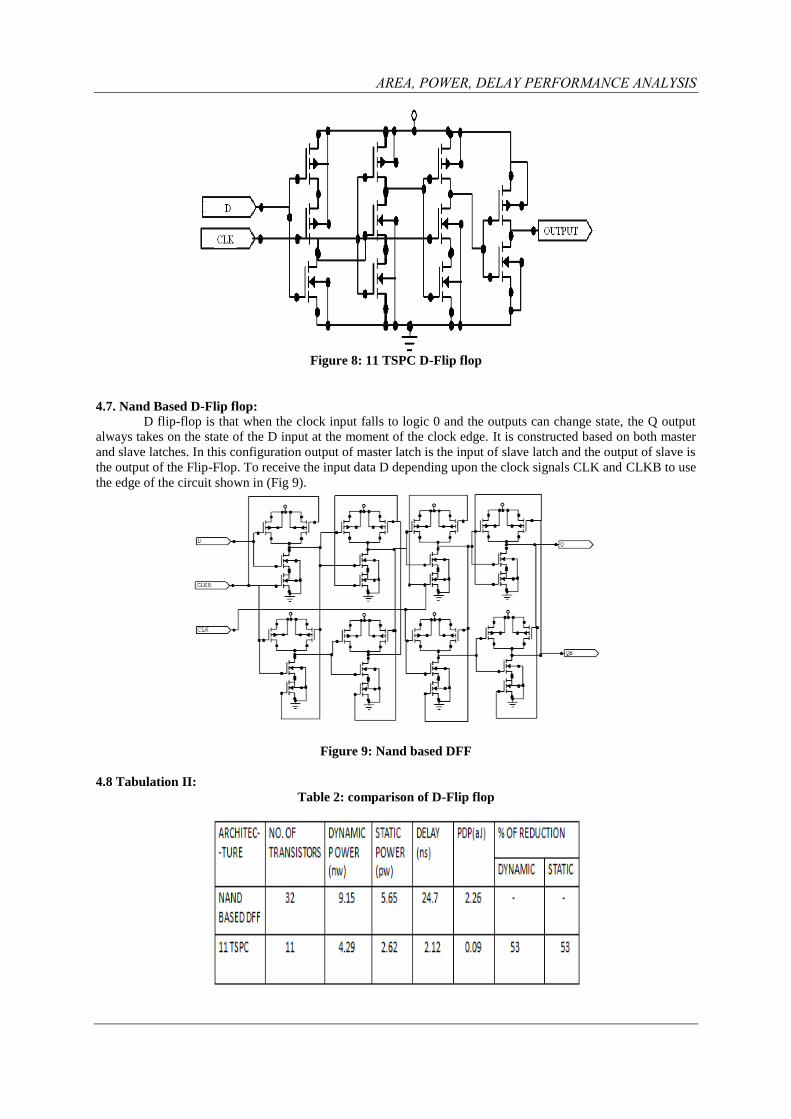
4.7. Nand Based D-Flip flop:
D flip-flop is that when the clock input falls to logic 0 and the outputs can change state, the Q output
always takes on the state of the D input at the moment of the clock edge. It is constructed based on both master
and slave latches. In this configuration output of master latch is the input of slave latch and the output of slave is
the output of the Flip-Flop. To receive the input data D depending upon the clock signals CLK and CLKB to use
the edge of the circuit shown in (Fig 9).
Figure 9: Nand based DFF
4.8 Tabulation II:
Table 2: comparison of D-Flip flop

AREA, POWER, DELAY PERFORMANCE ANALYSIS
From the power results in table 2, is observed that 11TSPC is efficient for dynamic and static power
and it produces less delay and Power Delay Product (PDP).
4.9 Standard 2 x 1 Multiplexer:
A two–to–one multiplexer is a combinational circuit that uses one control switch (S) to connect one of
two input data lines (A or B) to a single output as shown in (Fig.10).Only one of the input data lines can be
aligned to the output of the multiplexer at any given time. It‟s like sharing ice–cream on a date with one spoon.
Figure 10: Standard 2x1 Multiplexer
4.10 PTL Of 2x1 Multiplexer:
The pass transistor logic gives potentially very effective and uses less number of transistors. In (fig.11),
it reduces the count of transistors used to make different logic gates, by eliminating redundant transistors. If
several devices are chained in series in a logic path, a conventionally constructed gate may be required to restore
the signal voltage to the full value.
Figure 11: PTL of 2x1 Multiplexer
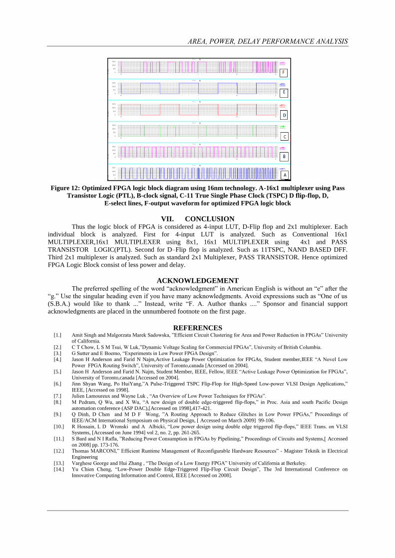
VI. OPTIMIZED FPGA LOGIC BLOCK: The optimized logic block consists of PASS TRANSISTOR BASED 16x1 MULTIPLEXER, 2x1
MULTIPEXER and 11TSPC D-Flip flop. First each individual block is analyzed. For each block any one
particular method is efficient compare to rest of methods. Hence combining the efficient method of each block.
Finally getting the Optimized FPGA Logic Block (Fig.12), this consumes less power and delay.
AREA, POWER, DELAY PERFORMANCE ANALYSIS
Figure 12: Optimized FPGA logic block diagram using 16nm technology. A-16x1 multiplexer using Pass
Transistor Logic (PTL), B-clock signal, C-11 True Single Phase Clock (TSPC) D flip-flop, D,
E-select lines, F-output waveform for optimized FPGA logic block
VII. CONCLUSION Thus the logic block of FPGA is considered as 4-input LUT, D-Flip flop and 2x1 multiplexer. Each
individual block is analyzed. First for 4-input LUT is analyzed. Such as Conventional 16x1
MULTIPLEXER,16x1 MULTIPLEXER using 8x1, 16x1 MULTIPLEXER using 4x1 and PASS
TRANSISTOR LOGIC(PTL). Second for D–Flip flop is analyzed. Such as 11TSPC, NAND BASED DFF.
Third 2x1 multiplexer is analyzed. Such as standard 2x1 Multiplexer, PASS TRANSISTOR. Hence optimized
FPGA Logic Block consist of less power and delay.
ACKNOWLEDGEMENT The preferred spelling of the word “acknowledgment” in American English is without an “e” after the
“g.” Use the singular heading even if you have many acknowledgments. Avoid expressions such as “One of us
(S.B.A.) would like to thank ...” Instead, write “F. A. Author thanks ....” Sponsor and financial support
acknowledgments are placed in the unnumbered footnote on the first page.
REFERENCES [1.] Amit Singh and Malgorzata Marek Sadowska, ”Efficient Circuit Clustering for Area and Power Reduction in FPGAs” University
of California.
[2.] C T Chow, L S M Tsui, W Luk,”Dynamic Voltage Scaling for Commercial FPGAs”, University of British Columbia.
[3.] G Sutter and E Boemo, “Experiments in Low Power FPGA Design”. [4.] Jason H Anderson and Farid N Najm,Active Leakage Power Optimization for FPGAs, Student member,IEEE “A Novel Low
Power FPGA Routing Switch”, University of Toronto,canada [Accessed on 2004].
[5.] Jason H Anderson and Farid N. Najm, Student Member, IEEE, Fellow, IEEE “Active Leakage Power Optimization for FPGAs”, University of Toronto,canada [Accessed on 2004].
[6.] Jinn Shyan Wang, Po HuiYang,”A Pulse-Triggered TSPC Flip-Flop for High-Speed Low-power VLSI Design Applications,”
IEEE, [Accessed on 1998]. [7.] Julien Lamoureux and Wayne Luk , “An Overview of Low Power Techniques for FPGAs”.
[8.] M Pedram, Q Wu, and X Wu, “A new design of double edge-triggered flip-flops,” in Proc. Asia and south Pacific Design
automation conference (ASP DAC),[Accessed on 1998],417-421. [9.] Q Dinh, D Chen and M D F Wong, ”A Routing Approach to Reduce Glitches in Low Power FPGAs,” Proceedings of
IEEE/ACM International Symposium on Physical Design, [ Accessed on March 2009] 99-106.
[10.] R Hossain, L D Wronski and A Albicki, “Low power design using double edge triggered flip-flops,” IEEE Trans. on VLSI Systems, [Accessed on June 1994] vol 2, no. 2, pp. 261-265.
[11.] S Bard and N I Rafla, ”Reducing Power Consumption in FPGAs by Pipelining,” Proceedings of Circuits and Systems,[ Accessed
on 2008] pp. 173-176. [12.] Thomas MARCONI,” Efficient Runtime Management of Reconfigurable Hardware Resources” - Magister Teknik in Electrical
Engineering
[13.] Varghese George and Hui Zhang , “The Design of a Low Energy FPGA” University of California at Berkeley. [14.] Yu Chien Cheng, “Low-Power Double Edge-Triggered Flip-Flop Circuit Design”, The 3rd International Conference on
Innovative Computing Information and Control, IEEE [Accessed on 2008].


![High Performance Logic Style with Constant Delay ... · traditional static and pass transistor CMOS logic ... domino (NORA domino) [3], zipper ... trendy logic style in high-performance](https://static.fdocuments.us/doc/165x107/5b7b4e627f8b9adb4c8c5a93/high-performance-logic-style-with-constant-delay-traditional-static-and.jpg)