Architecture Specification for Acutiator - thule.no · 3.5.3 The Interrupt Vector Manager ... 5.7...
114
Architecture Specification for Acutiator Fourth Generation Amiga System Document Revision 7.0 October 18, 1992 by Dave Haynie Greg Berlin Scott Schaeffer
Transcript of Architecture Specification for Acutiator - thule.no · 3.5.3 The Interrupt Vector Manager ... 5.7...
Architecture Specificationfor
AcutiatorFourth Generation
Amiga System
Document Revision 7.0
October 18, 1992
byDave Haynie
Greg BerlinScott Schaeffer

This paper contains unpublished trade secrets and other stuff you're probably not supposed to be reading. It may not be reproduced in any form outside of Commodore without the express written permission of Commodore International Services Corporation, Technology Division.
Copyright 1991, 1992 by Commodore International Services Corporation, Technology Division.
All text and graphics herein were created by Dave Haynie. Ideas were coelesced by Dave Haynie, with the possibly unintentional help of Greg Berlin, Scott Schaeffer, Mike Sinz, Randell Jesup, Chris Green, Hedley Davis, and undoubtedly others who'll be added here once I find out who they were.
This paper was developed entirely on Amiga computers. It was electronically published with the PageStream V2.2 program from Soft-Logik Publishing Corporation. All graphics were drawn with the Professional DrawTM V2.0 program, from Gold Disk.

V7.0 Architecture Specification for Acutiator 3
Forward
It's the end of the world as we know it, and I feel fine- R.E.M.
This paper is a concerted effort to define and document a new, advanced Amiga system architecture. It represents the authors' best proposal for such a system based on their numerous years of designing computers and defining system architecture at Commodore. It is also the result of numerous consultations with Amiga experts in various areas of expertise, including those involved in chip and software design as well as hardware design. We are, after all, defining a system architecture here.
Since this is an architecture specification, there's a considerable amount of material to cover before any actual system is described. If you're more interested in a bottom line answer to “what does all this give me”, please feel free to skip ahead to Chapter 8. But please keep in mind that the system described in Chapter 8 is one possible suggested chip/system implementation of the architecture. One main point of this new design is that any number of different system configuations are possible based on the same system chips.
I hope that this point isn't lost. Commodore has a bad habit of stumbling blindly into new system designs, taking just enough time to prevent a fall. This makes system designs that are really viable for only one system. I started this effort over a year ago in an attempt to get something better than that down on paper, all thought out, before it was actually needed. I hope the implementors of this, whomever they turn out to be, can appreciate this and avoid chopping out features just because they aren't clearly needed for one system.
Dave HaynieOctober 23, 1991

4 V7.0Forward
V7.0 Architecture Specification for Acutiator 5
Contents
1 INTRODUCTION1.1 The Shortcomings of Previous Systems1.2 The Acutiator Architectural Goals1.3 Basic Assumptions1.4 A Note To Implementors1.5 A Note To Reviewers
2 THE ACUTIATOR SYSTEM2.1 The AMI Bus2.2 The Host Subsystem2.3 Alternate Processors2.3.1 Other Host Processors2.3.2 The SCSI Processor2.3.3 The Signal Processor2.3.4 The Video Compression Processor2.4 The Motherboard Subsystem2.4.1 The Motherboard Controller2.4.2 The DRAM Bus Slot2.4.3 The AMI Bus Slots2.4.4 Other Motherboard Slots2.5 The Amiga Chip Subsystem2.6 The Expansion Subsystem2.8 Memory Organization
3 THE MOTHERBOARD CONTROLLER3.1 The JTAG Test Port3.2 The AMI Bus Interface3.3 The Reset Manager3.4 The Primary Bus Arbiter3.5 The I/O Subsystem3.5.1 The 8-Bit Peripheral Bus3.5.2 The I/O Select Manager3.5.3 The Interrupt Vector Manager3.5.4 The SSPB Bus3.5.5 The Memory Card Interface3.6 The Coprocessor Interface3.7 Motherboard Controller Summary3.8 The AMOS Chip Implementation
1-11-11-21-31-31-4
2-12-12-32-32-32-42-42-42-52-52-52-62-62-62-72-7
3-13-13-23-23-33-43-43-53-63-73-73-83-93-10
6 V7.0Contents
3.9 MC68020/MC68030 Bus Support3.11 RISC/Alternate Processor Bus Support3.11 Register Map3.11.1 System Control3.11.2 System Time Counter3.11.3 SSPB Registers3.11.4 I/O Control3.11.5 I/O Timer3.11.6 Interrupt Control3.11.7 DMA Control3.11.8 Coprocessor Control3.12 PCMCIA Registers3.13 Memory Mapping
4 THE AMIGA CHIP CONTROLLER4.1 JTAG Test Port4.2 The AMI Bus Interface4.3 The Chip Bus Interface4.4 The Chip Bus Arbiter4.5 The Chip RAM Interface4.6 Special Functions4.7 Amiga Chip Controller Summary4.8 Notes on SAIL History4.9 The SAIL “AAA” Chip4.10 Register Mapping4.10.1 The ID/Version Register4.10.2 SAIL Control4.10.3 Chip Register Base4.10.4 Chip RAM Base4.10.5 Chip RAM Configuration4.10.6 The Plane Conversion Mechanism4.10.7 The Data Conversion Table4.10.8 Chip RAM Timing4.11 Decode Mapping
5 THE EXPANSION CONTROLLER5.1 The JTAG Test Port5.2 The Clocks5.3 The AMI Bus Interface5.4 Host Arbitration Signals5.5 The Zorro Bus Interface5.6 Zorro Master/Slave Control5.7 PIC Support Mode5.8 Expansion Controller Summary5.9 The EPIC Chip
3-103-133-133-133-153-153-163-173-183-193-203-213-21
4-14-14-14-24-34-44-54-54-64-74-74-84-94-104-104-104-114-114-124-12
5-15-25-35-35-45-45-55-65-85-9

V7.0 Architecture Specification for Acutiator 7
5.10 Register Map5.10.1 The ID/Version Register5.10.2 Expansion Control5.10.3 DMA Registers5.10.3.1 DMA Indirect5.10.3.2 DMA Source5.10.3.3 DMA Destination5.10.3.4 DMA Count5.10.3.5 DMA Control5.10.4 Channel Control5.10.5 AUTOCONFIGTM Control5.10.6 Com Control5.10.7 Com Data5.11 Memory Mapping
6 THE CPU/RAM CONTROLLER6.1 The JTAG Test Port6.2 The MC68040 Bus6.3 The AMI Bus Interface6.4 The DRAM Controller6.5 The Bus Arbiter6.6 Other Local Functions6.7 CPU/RAM Controller Summary6.8 The RACE Chip Implementation6.9 Register Map6.9.1 The ID/Version Register6.9.2 Configuration Control6.9.3 DMA Control6.9.4 Coprocessor Communications6.9.5 RAM/ROM Control6.9.6 RAM Base6.9.7 Refresh Control6.9.8 RAM Timing6.9.9 Interrupt Control6.10 Memory Mapping
7 THE AMI BUS7.1 Component Signals7.1.1 The Clock Group7.1.2 The Phase Ø0 States7.1.3 The Phase Ø1 States7.2 Bus Timing7.3 Bus Transactions7.3.1 Pseudo-64-bit Cycles7.3.2 Wait States
5-105-115-125-125-125-135-135-135-135-145-155-175-185-18
6-16-16-26-36-46-66-76-76-96-96-106-106-126-126-136-146-146-146-146-15
7-17-17-27-27-47-57-67-67-7

8 V7.0Contents
7.4 Coprocessor Override Cycles7.5 The AMI Bus Physical Connector7.5.1 General Support Signals7.5.2 Bus Arbitration Signals7.5.3 Coprocessor Support Signals7.5.4 Test Port Signals7.5.5 System I/O Signals7.5.6 The AMI Bus Slot Pinout
8 AN EXAMPLE SYSTEM8.1 The Highly Modular System Concept8.1.1 A Brief History of Modularity8.1.2 Modularity and the Amiga8.2 A Highly Modular Motherboard8.3 Some Processor Modules8.4 The Amiga Module8.5 The Expansion Module8.6 The Coprocessor Module8.7 Physical Design Concepts
7-77-87-87-97-97-107-107-11
8-18-18-18-28-38-58-68-88-98-9
V7.0 Architecture Specification for Acutiator 9
Tables & Figures
Figure 2-1 Example Acutiator System Block Diagram 2-2Figure 2-2 Example Acutiator System Memory Map 2-8
Figure 3-1 AMOS Chip Block Diagram 3-11Figure 3-2 AMOS Register Map 3-12Figure 3-3 The AMOS ID/Version Register 3-13Figure 3-4 System Control Register 3-14Figure 3-5 SSPB Registers 3-15Figure 3-6 I/O Control Register 3-16Figure 3-7 I/O Timer Register 3-17Figure 3-8 I/O Timing Effects 3-18Figure 3-9 Interrupt Control Register 3-19Figure 3-10 DMA Control Register 3-20Figure 3-11 Coprocessor Control Register 3-20
Figure 4-1 The AAA SAIL Chip 4-7Figure 4-2 SAIL Register Map 4-8Figure 4-3 The SAIL ID/Version Register 4-9Figure 4-4 The SAIL Control Register 4-9
Figure 5-1 The EPIC Chip 5-9Figure 5-2 EPIC Register Map 5-10Figure 5-3 The EPIC ID/Version Register 5-11Figure 5-4 The Expansion Control Register 5-11Figure 5-5 The DMA Control Register 5-13Figure 5-6 The Channel Control Register 5-15Figure 5-7 AUTOCONFIGTM Control Register 5-16Figure 5-8 Com Control Register 5-17
Figure 6-1 RACE Chip Block Diagram 6-8Figure 6-2 RACE Logical Register Map 6-9Figure 6-3 The RACE ID/Version Register 6-10Figure 6-4 The Configuration Control Register 6-10Figure 6-5 The DMA Control Register 6-11Figure 6-6 The Coprocessor Communications Register 6-12Figure 6-7 The RAM/ROM Control Register 6-13
Figure 7-1 Basic AMI Bus Cycle 7-6Figure 7-2 Pseudo 64-Bit Cycles 7-7

10 V7.0Figures
Figure 7-3 Wait States 7-8
Figure 8-1 An Example Highly Modular System 8-4Figure 8-2 Example Processor Modules, Simple and Multimedia 8-6Figure 8-3 An Example “AAA” Amiga Module 8-7Figure 8-4 The Expansion Module 8-8Figure 8-5 A HIghly Modular Motherboard 8-10
V7.0 Architecture Specification for Acutiator 1-1
Chapter 1Introduction
The original 68000-based Amiga systems were designed with the philosophy that the main components of an Amiga system could be part of a reasonably small number of custom integrated circuits. This would facilitate both lower system cost and higher system performance than traditional TTL based designs. At the time, it came very close to achieving this goal.
Since that time, there has been more system design work aimed at building Amiga systems of increasing power without any loss in the price/performance ratio of the system. The Amiga 3000, the lastest example of this design effort, comes in as a very high performance 68030 system at a personal computer price.
However, the rest of the world has not been standing still. The techique of “design by chip” has been picked up by most computer companies, as chip design firms release highly integrated system glue parts for large subsystems in standard architectures, and gate arrays continue to grow in size and drop in price. The rules of competition have been rewritten. Thus, a corresponding rewriting of Amiga system architecture is required to create new Amiga systems that do well on the industry-wide price/performance curve of the 1990's.
As the system architects of the Amiga 3000, we are in the best position to evaluate the shortcomings of the A3000 and propose a replacement architecture, no one else knows Amiga systems design better. We mention the A3000 simply because it is currently the architectural basis for all mid and high end Amiga systems. We acknowledge the reality that today, the “high-end” price point necessary for viable competition should be below the A3000 levels for an entry level high end system. Our competition makes this perfectly clear.
1.1 The Shortcomings of Previous Systems This docment describes the Acutiator Architecture. While this is an architecture
specification, not a system specification, we do intend to get some details of the basic system chip set, and examine some system designs based on this system chip set.
We find a few problems with the current high-end Amiga hardware architecture. One of the main problems is that it isn't modularized. We based a great deal of the partitioning of the A3000 system on what had been done in second generation Amiga systems. and also on the available resources, in manpower and chip technology, available in 1989. We find the A3000's expansion bus controller responsible for motherboard bus arbitration, and the A3000 motherboard controller responsible for a good bit of the Amiga chip interface. While that worked reasonably well for the A3000 initially defined, it's not easy to modify this setup. A system without an expansion bus needs to provide its own arbiter for the main bus. A system using an “AAA” display subsystem completely bypasses the chip bus control logic in the

Chapter 1: Introduction V7.01-2
motherboard controller.
Another set of problems with the A3000 are found in its I/O chip definition. While all the A3000 system chips work pretty well to build an A3000 as defined, they make it costly to deviate from this definition. Adding any additional I/O around the A3000 custom chips add considerable expense in fast PAL devices. For example, the Amiga 4000 uses the A3000 architecture with an IDE hard drive interface rather than the fast SCSI of the original system. Yet, with the cost of hooking IDE into the A3000, this is not a great cost savings -- IDE should be virtually free of cost.
The other problem with the current architecture is that of performance. While the Amiga 3000 is a good representative of a 68030 system, it makes some performance compromises. Memory and SCSI, for example, have improved considerably since then. Most of these were well understood and considered necessary, based on the available technology at the time of the system's design. Today, they can be overcome, and with a proper new architecture, room for such advances can be properly made in advance, rather than ignored or hacked in at a later date.
1.2 The Acutiator Architectural Goals
The main idea of the Acutiator Architecture is to define some system building blocks for building high performance 68040 systems that can also meet some low cost goals. Toward this end, things are designed to be modular. The architecture doesn't depend on the specific kind of Amiga chip set. It defines an interface device that encapsulates any specifics of the chip set architecture, eliminating the need to consider this in the rest of the system. Given the rapid advance of both CPUs and Amiga chips these days, it is possible we will have Acutiator systems using “AA”, “AA+”, and “AAA” graphics chips, with 68040, 68060, and even RISC host processors.
For motherboard management, the Acutiator Architecture defines a motherboard controller. This device generates chip selects for stand-alone chips, such as general I/O, IDE, SCSI, or LAN controller units. It manages arbitration of the compact CPU-independent “System” bus, providing general purpose bus channels that may be used for CPU, DSP, SCSI, Zorro bus, and other expansion. It does the bus sizing necessary to let modern 32-bit and 64-bit bus masters communicate with standard 8 or 16-bit peripherals.
The CPU-bus specifics are encapsulated on the processor module. This module provides a system bus interface for the main CPU, and also drives the DRAM bus. The DRAM bus controls a DRAM subsystem located on the motherboard, yet all control signals originate on the main CPU module . This permits the memory interface to be optimized for the particular main processor, perhaps the most critical performance element in the system. The DRAM bus is a 64-bit bus with support for interleaved memory banks and a large amount of SIMM module based page-mode memory of just about any speed.
Finally, the optional expansion bus device manages high speed conversion between System bus protocols and the Amiga Zorro II/Zorro III bus, including all necessary buffering, synchronization, and bus sizing. This is designed to make the full 32-bit Zorro III bus a much

V7.0 Architecture Specification for Acutiator 1-3
lower cost system option, and much easier to remove from systems that don't require expansion.
Acutiator is the first complete Amiga system level design that was architected with both modulatity and flexibility in mind. We found that building mid-range systems from A3000 system chips, for example, actually required extra parts, since the A3000 system chip set was designed specifically to make A3000s. Acutiator chips will permit a number of different systems to be created using the same chip set, without the need for extra glue at either the low or high end. In fact, one highly modular Acutiator-based platform can easily fill both mid and high end requitrements. The system designer can build a mid-range system with little more than Acutiator chips, Amiga chips, memory, and buffers. High end systems simply bolt on extra modules, like DSP, SCSI, or Expansion Bus, as the system specification demands. Modules can be supported either as motherboard interconnects or actual add-in cards with very low interface overhead compared to full fledged Zorro bus cards.
1.3 Basic Assumptions
There are obviously a few basic assumptions about available resources inherent in the Acutiator specification. Of primary concern is the definition of the various system chips required in an Acutiator system. While the chip architectures aren't necessarily tied to the implementations suggested herein, we do consider the suggested implementations to be optimal. The three proposed gate arrays represent a compromise between cost effectiveness and agressiveness. The functionality of a gate array can, within limits, rise non-linearly with pin count. However, the price point of a gate array is determined by gate count and packaging, which tends to run contrary to function density.
As far as packaging goes, the costs rise sharply when the design is too large to fit in a plastic package. Using commonly available surface mount PQFP package sizes, we set a limit of 160 pins on any given part. This limit also works out to fit in well with our goal of the nicely modularized chip implementation, necessary to properly implement a modular platform. Since most of the content of each Acutiator system chip is devoted to control logic and data routing, the gate densities in the range of 20,000 gates should be sufficient for any Acutiator chip. Finally, speed requirements will make 0.8um-1.0um CMOS capability necessary.
1.4 A Note To Implementors
This is, of course, a preliminary specification. If you're designing a particular chip or piece of a chip, you have some significant input on the nature of what you're designing. If something seems wrong, maybe it is. But please don't fix it secretly. Propose the changes to the Acutiator design committee, or, in the absence of such a committee, tell Dave Haynie what you're changing. This specification could influence the work of lots of people for a long time. We don't want any nonsense creeping in or left in, but we want to make sure any who should know what's going into these chips does know. The only way that can happen is if we keep the specifications current.
Each chip has its own chapter, and elements of them are described elsewhere. If you're building a chip and willing to keep the documentation up to date as a part of the Acutiator

Chapter 1: Introduction V7.01-4
specification, feel free to take over ownership of your particular chapter. If not, Haynie will maintain them as before. If you're desigining a chip, you will need to write a full specification for it, so there may be a good starting point in the associated chapter in any case. Should we split up the documentation this way, it'll be important to keep the specification up to date as things change, no matter how busy it gets actually doing the work. A good Amiga DTP system at hope may be a big hand here.
1.5 A Note To Reviewers
If you have been asked to look this over, please do with as much care as possible. Certainly not every reviewer is going have expertise in every area, but at least try to make sure that the areas you do have thoughts on get some attention. Even if you're reviewing this without specifically being asked, we'd appreciate any feedback. There's usually something that looks like a good idea to some and pure folly to others. The goal is to have this whole specification, and the chips it helps generate, seem like good ideas to everyone who comes across them.
2-1V7.1 Architecture Specification for Acutiator
Chapter 2The Acutiator System
An example Acutiator system diagram is shown below in Figure 2-1. This is representative of a system with many of the supported options, though its certainly just one way to assemble a complete Acutiator system. The display subsystem is not specified -- it could be the “AA” chip set, “AAA”, XGA, TIGA, or virtually anything else). An interface chip encapsulates the specifics necessary to mate any custom chip subsystem to the AMI bus.
The example system shown consists of the Amiga chip subsystem, three off the shelf main bus masters, and four new Commodore designed gate arrays. There are also some buffers and a few external glue logic chips. Some other desired I/O devices can be accomodated via programmable I/O selects or slight modifications to the particulars of the system chips suggested herein.
2.1 The AMI Bus
The Acutiator system is centered around the Acutiator Modular Interconnect, or AMI bus, rather than any CPU-specific Local bus. It's important in any large system, such as Acutiator, that the designs generated be as modular and reusable as possible. The bus interface could certainly be processor specific, but in the past this hasn't proven to be optimal. The Amiga 3000 gate arrays, for example, were MC68030 bus-specific. Little to none of their design can be reused on the Acutiator project, most of it was based around MC68030 specifics that aren't very easy to support with other 680x0 chips, RISC chips, etc. The other problem is that the full MC68030 bus took too many pins on a gate array to fully support in each part, so compromises were made in the system design to deal with this.
The AMI bus is based somewhat on the MC68040 bus protocols. However, the bus uses multiplexed Address/Data and Master/Slave signal groups to provide a much more compact interface, ideal for chip to chip interconnects. It also supports enhancements to allow it to mesh cleanly with alternate processors such as DSP or SCSI, as well as future MC680x0 or RISC processors, including 64-bit processors. Even the MC68020 or MC68030 can drive the AMI bus with a minimum of glue logic.
The definition of such a generalized high speed interconnect has been a target goal of the Systems group since before the MC68040 was released; it allows system designs to be reused much more readily, and it opens the door to highly modularized systems impossible or impractical using past interchip interconnects. Such a highly modular Acutiator system will not have any processor-specific bus, only AMI bus slots and a RAM interface slot. More compact non-modular systems can still run a processor bus on the motherboard with no loss of system efficiency. A full specification of the AMI bus is provided in Chapter 7.

2-2 Chapter 2: The Acutiator System V7.1
Figure 2-1: Example Acutiator System Block Diagram

2-3V7.1 Architecture Specification for Acutiator
2.2 The Host Subsystem
All Acutiator systens will have some kind of Host subsystem. There are a couple of possible physical implementations of the Host subsystem. There always be some kind of main processor, which is the primary bus master on the Host, or Local Bus. In most cases, a local bus controller will permit alternat local bus masters, and drive the interface for the particular Local Bus to AMI bus conversion. The Local Bus can be located on the motherboard, but in any modular system it exists only on an AMI bus card. Such a modular system will have a “host” slot, which is the standard AMI bus slot in-line with a 64-bit DRAM bus slot.
The initial Acutiator system has the primary goal of supporting a fast MC68040 CPU. To this end, it defines a Host/Memory Controller device that interfaces the MC68040 bus to the Acutiator DRAM bus and AMI bus. This device is designed to support all forms of the MC68040 at 25MHz to 40MHz. It is expected to provide support for the standard MC68040, the MC68LC040 (low-current mode only, no FPU), and optionally, the MC68030 and MC68020 (of possible concern for low cost implementations).
Some host modules will also contain alternate processors. There may be some advantage to locating certain kinds of processors on the MC68040 (or other host-specific) local bus. The AMI bus is designed for simple and flexible interface to a variety of 32-bit processors, but obviously, any device designed specifically for the MC68040 bus will work better on the MC68040 bus.
2.3 Alternate Processors
The Acutiator system supports various alternate processors. The example shown locates two alternate processors on the host module, but it's possible to have such devices on the AMI bus just as easily. In some cases the host module can make such devices easier to add, while the AMI bus makes the modularization of such devices easier. It's the job of this architecture to leave such a decision to the system designer. This sections covers some suggested module options.
2.3.1 Other Host Processors
The Host/Memory controller device is responsible for the host processor implementation. For efficiency and cost reasons, such a controller device is specified as a gate arrary for the initial instance, the MC68040 version. Neither the memory nor the AMI bus interface is necessarily so complex as to require an integrated solution, though. Alternate processors can generally be hooked to the AMI bus and/or DRAM bus with a small number of PAL and buffer devices.
Host processors can follow the MC68040 convention of actively requesting the bus when its needed. A programmable parking option permits easy support of the MC68020/30 convention of acting as a default bus master. System-wide support of various burst lengths allows both 32-bit and 64-bit processors to easily hook up to both the AMI bus and the 64-bit DRAM bus. Most of the AMI bus protocols, while derived from MC68040 conventions, are easy to generate for other processors.

2-4 Chapter 2: The Acutiator System V7.1
2.3.2 The SCSI Processor
DMA-driven SCSI disk I/O is an important option for high performance Acutiator systems. Several possible SCSI controllers may be easily hooked into the system. For high performance we recommend the NCR 53C710 SCSI-2 controller, which can be interfaced to either the AMI bus or an MC68030/MC68040 Local bus. This controller handles SCSI far more efficiently than traditional Amiga SCSI, both via SCSI transfers far more efficient than a Western Digital SCSI chip, and by offloading main processor overhead via an on-chip programmable SCSI processor. It supports the SCSI-2 protocol, including 10MB/s fast synchronous mode. Alternately, an 8-bit programmed I/O SCSI chip may be attached to the I/O bus, for a very low cost, low performance SCSI interface. The I/O bus can also support a nearly glue free IDE bus implementation.
2.3.3 The Signal Processor
A signal processor is a vital option for Acutiator Multimedia systems. The AT&T DSP3210 is a low cost, high performance bus mastering signal processing coprocessor ideally suited to the Amiga hardware/software architecture. This processor has two main functions. As a mathematics engine, it can process single-precision floating-point up to ten times faster than a standard MC68040 running optimized 68040 code, or as much as fifty times faster than a 68040 running Amiga IEEE libraries or 68030 floating-point code. The standard AT&T software modules provide, in the context of a real-time multitasking operating kernel, a great number of standard functions, including sampling rate conversion, JPEG decoder, and both audio and video MPEG decoders, with many other modules available optionally.
As an I/O processor, the DSP3210 has a very efficient interface to a high speed serial bus, which supports peripherals such as CODECs for CD and DAT compatible hi-fi audio, standard high speed telecommunications protocols such as V.32, or standard digital audio transfer protocols such as AES/EBU. The DSP3210 will be a crucial addition to any Amiga system intended for Multimedia authoring. Most such computers will employ DSP within the next two years, we know of nothing at any price that integrates under any other hardware/OS combination as well as this subsystem. A DSP3210 can be easily interfaced to either the AMI bus or a MC68030/MC68040 Local bus.
2.3.4 The Video Compression Processor
Another device worthy of consideration in an Acutiator system is a video compression processor. Modern multimedia computing has found an increasing need for high speed video record and playback from low bandwidth mass storage such as CD-ROM. The DSP can provide fast but non-realtime encode and decode of such compressed imaging. For realtime operation, compression processors may often be interfaced directly to the motherboard I/O bus, while a compression processor with bus mastering capability would find a good home on the AMI bus. This is a very active field at present -- solutions are emerging from several different companies. No particular recommendation for video compression processor is made in this specification.

2-5V7.1 Architecture Specification for Acutiator
2.4 The Motherboard Subsystem
All Acutiator systems are centered around a Motherboard subsystem. The goal of the Motherboard subsystem is to provide all of the services necessary to any basic Acutiator system, without supplying any options that won't be used by all board implementations. This includes DRAM and standard I/O management, with room for simple I/O options that vary by Motherboard implementation. A modular Acutiator motherboard will have AMI bus slots, a single DRAM bus slot, and some special I/O bus slots for routing specific-purpose signals between the motherboard and at least some AMI bus modules. Non-modular systems can arrange things however they see fit, but in general, very little glue is necessary for a wide variety of possible configurations.
2.4.1 The Motherboard Controller
The Motherboard Controller is responsible for managing just about everything that goes on a modular motherboard. Its main features are as follows:
• Main arbiter for AMI bus access.• Interrupt manager and arbiter for vectored interrupts• Chip selection for all motherboard ROM and I/O, with a flexible programmble
select system.• Peripheral bus interface for 8-bit I/O devices.• SSPB serial bus for simple serial I/O (I2C, InterMetal, Access.Bus).• Multiprocessor control port for AMI bus residernt alternate processors.• System reset management.
This device allows a system to be constructed that follows the strict Amiga philosphy of “no waiting”, yet it has nothing specific to the traditional Amiga chipset to it. For example, using the programmable I/O selects, a complete UNIX machine could be constructed with a MC68040-base host module, the Motherboard Controller, a 32-bit SIMM memory module, a few buffer chips, a boot ROM, and off-the-shelf disk and video chips. This could also be used to make low cost non-video Amigas with standard parts once an RTG subsystem exists for the Amiga OS.
2.4.2 The DRAM Bus Slot
The Acutiator system tries to walk a fine line between low cost, high performance, and flexibility. The AMI bus provides decent performance for most things and permits chip to chip interfaces that are low cost, full featured, and CPU independent. The one place in any system a processor-specific interface can have the most beneficial performance effect is the DRAM interface. Toward this end, modular Acutiator systems have a special DRAM slot.
This DRAM slot provides for a 64-bit DRAM bus with up to 128MB of fast, interleaved, SIMM-based memory. This slot is expected to be provided in-line with the first AMI bus slot, the “host” module slot. The host module can thus optimize the DRAM interface for the host processor without the need to house space-consuming DRAM on every host module. The host module is responsible for running AMI bus to DRAM bus accesses.

2-6 Chapter 2: The Acutiator System V7.1
2.4.3 The AMI Bus Slots
As with most mid-to-high-end Amigas, the Acutiator systems support the basic idea of a coprocessor slot. This slot provides a number of signals for high-speed system enhancements. Unlike previous Amiga systems, the Acutiator Modular Interconnect, or AMI bus. is fully buffered and optimized for chip to chip interconnects. This permits several open AMI slots, rather than the single [co]processor slot of the A3000/A4000. The AMI bus slot is, as described, this more general purpose high speed modular expansion bus. It allows additional CPUs to be added in multiprocessor clusters. It allows the addition of more AT&T DSP3210 processors, or the addition of the first DSP3210 in a base system that leaves that processor out. This slot technically also permits the addition of more fast 32-bit memory (though never as fast as that on the 64-bit DRAM bus), though with up to 128MB supported by the motherboard, other uses are more likely.
Perhaps more interestingly, Acutiator system chips, with the exception of the basic System Controller, can live on an AMI bus card as easily as on the motherboard. This is another feature that makes possible the concept of a highly modular system, such as that outlined in section eight. Highly modular Acutiator machines will have several AMI bus slots.
2.4.4 Other Motherboard Slots
While some other subsystems obviously define slots of their own, some Acutiator systems will have additional motherboard expansion slots. Specifically, highly modular systems will leave video and some other I/O off the motherboard. To facilitate the addition of these items via modules, extra expansion mechanism are necessary. There are two basic types of I/O support slots envisioned. The first of these will bring out the general purpose I/O bus defined by the Acutiator system controller. This will allow some kinds of I/O devices to be added in modules for much less cost than in a general purpose expansion card. Things considered basic motherboard extensions in a highly modular Acutiator system can go here, most expansion still belongs in Zorro cards.
The other type of I/O support slot needed is essentially a slot with most of the the motherboard I/O lines available on it. This allows the various I/O signals, like floppy ports, CIA port lines, digital video, etc. to be drawn from different modules and routed to where they're needed in the system. In some cases, two modules need only communicate with one another. In this case, its expected that they'll cable between one another rather than route through the motherboard. This allows things like digital video expansion slots, pixel bus expansion slots, or things we haven't even imagined yet to be added to existing Acutiator systems via new modules. These generally, but not exclusively, pertain to Amiga chipset expanison options. The final physical form of this expansion depends on the final physical form of an Acutiator system itself.
2.5 The Amiga Chip Subsystem
The Acutiator's chip bus is managed by the Amiga Chip Controller device. This device is completely responsible for gating the AMI bus master onto a Chip bus. It manages all Chip-related memory decoding, data burst, buffering, latching, cache control, and cycle termination for

2-7V7.1 Architecture Specification for Acutiator
its target Amiga chip subsystem. In general, such a device can greatly enhance the processor to Chip RAM bandwidth of an Amiga system versus typical Gary plus PAL interfaces used today.
Different versions of the Amiga Chip Controller will exist for each Amiga chip set we would like to connect to an Acutiator system. I expect the emphasis today to be primarily on the AAA chip set, but there's nothing mandating only AAA systems. The AAA chipset is designed to work well with 32-bit systems, and as such should connect to the AMI bus using just the AAA version of the Amiga Chip Controller and perhaps a small number of buffers or latches.
The AA Chips could just as easily be connected to the AMI bus, given an AA version of the Amiga Chip Controller. For such an implementation, though, we suggest the help of a second simple gate array, the complex buffer device. This device manages the data path between the System Bus, the Chip bus, and two 32-bit wide banks of DRAM. Together, these chips manage all data bus bridging and sizing, write latching and burst access to Chip RAM, and a special interleaved access that gives the Acutiator System Bus master a path to Chip RAM roughly twice that of the Amiga 3000, even when full video saturation takes place. With proper I/O Bus support on the motherboard, the Amiga Chip Subsystem can comfortably live as an a module in a highly modular Acutiator system.
2.6 The Expansion Subsystem
For systems with an Expansion bus, the Expansion Controller manages conversions between AMI and Zorro bus protocols. This includes all the buffering and bridging necessary to support the 16-bit Zorro II bus, Zorro II DMA onto the AMI bus, the 32-bit Zorro III bus, and Zorro III DMA onto the AMI bus. The Zorro III protocol converter uses a four word bidirectional FIFO to effectively pipeline the bus protocol conversions when burst-mode transfers are made between the AMI bus and the Zorro III bus. This device also provides an efficient DMA controller intended for, but not limited to, high efficiency transfers between the AMI and Zorro buses. With proper motherboard or Amiga module video bus support, the whole Expansion Subsystem can live comfortably as an add-in module.
2.7 Memory Organization
The system memory configuration depends largely on the system configuration and initialization. Most system I/O lives in reserved 64K I/O slots, located in the standard I/O areas used in previous Amiga systems. ROM and Chip RAM have compatibility locations as well as extended mappings, and Chip RAM's extended mapping can be any 16MB region of memory, though a suggest region is shown. Fast RAM can as well be assigned a memory address, though a suggested one is shown. Several Zorro III mappings are also available. AMI bus slots are given fixed 16MB memory chunks and 64K I/O chunks. A memory map showing most of the possible memory areas is shown in Figure 2-2.

2-8 Chapter 2: The Acutiator System V7.1
Figure 2-8: Example Acutiator System Memory Map
V7.3 Architecture Specification for Acutiator 3-1
Chapter 3The Motherboard Controller
The Motherboard Controller device is the main bus controller for the Acutiator system. It manages all aspects of the non-Amiga-chipset-related motherboard operation. This device replaces and enhances some of the functions of the Amiga 3000 system chips Gary, RAMSEY, and Buster. The specification is intended to permit low cost Amiga systems to be designed around a common, high-speed chip interconnect bus (the AMI bus), while at the same time affording the system designer more control of actual system component makeup than the Amiga 3000 architecture easily permitted.
This chapter first describes the basic signal and functional requirements of any Acutiator Motherboard Controller block, then specifies a preferred implementation, the AMOS chip. Finally, the register map for the AMOS chip is provided, with a list of the register assignments and functions associated with these requirements. There is some room for pinout flexibility in alternate implementations and, similarly, some register map flexibility.
Perhaps the most unusual aspect of this controller, in relation to previous Amiga motherboard control devices, is its flexibility. This device is designed to handle a large variety of memory and I/O devices with little or no added glue logic. To support this flexibility, there's a great deal of programmbility, and thus a great deal of programming necessary to set up the I/O system for wait states, bus protocol, etc. The system ROM programs these critical bits only on power up, then invokes a lockdown bit which forces them into a fixed state until the next powerdown, insurance against errant or malicious programs when running unprotected OSs.
3.1 The JTAG Test Port
As in all Acutiator chips, a test port for the IEEE P1149.1 boundary scan protocol is defined. While such a port isn't vital to the operation of the device, we're convinced that board-wide JTAG support will be useful for both Chip and System testing. The pin requirements are:
Signal(s) CountClock 1Mode Select 1Data 2Reset 1
TOTAL 5
The actual test register map will be defined based on the chip implementation, it doesn't belong in this architecture specification. However, we do expect any implementation will at the least support the normal boundary scan functions.
Chapter 3: The Motherboard Controller V7.33-2
3.2 The AMI Bus Interface
The full AMI bus goes to the Motherboard Control device. This allows the device to do full 32-bit decoding of the addresses in order to directly drive all of its various I/O supports. Additionally, this interface allows it to support a number of full 32-bit configuration and control registers. The full 32-bit data bus also allows it to manage data byte funneling for the 8-bit I/O bus it supports. The initial pin count estimate for this section is:
Signal(s) CountClocks 3Address/Data Bus 32System Bus Control 11
TOTAL 38
There really aren't many options in this section. In theory, an advanced version of the device could contain some intelligent DMA for I/O management. Obviously, any extensions to the System Bus protocol must go here, which might include additional support for alternate host processor buses. Interrupt synchronization could also go here if pins were available, but its very simple to support extenally.
System Bus Signals
BCLK Main bus clock, 25MHz-50MHz.DCLK Double-speed clock, 50MHz-100MHzØ AMI bus phase clock.AD31-AD0 Main multiplexed address/data bus, synchronously multiplexed based on the
BCLK and Ø.MS10-MS0 Multiplexed master/slave control signals.
3.3 The Reset Manager
As in most Amiga systems, there are various aspects of system reset to consider in an Acutiator system. The Motherboard Controller is responsible for managing reset. On powerup, it monitors a power stability input, and waits with the full and I/O reset lines asserted until this signal indicated power stability. Once power is stable, the controller initiates the full-system reset condition. The full-system reset condition causes the controller to assert its full-reset output for the standard Amiga reset count. When not driving the full reset line, the controller monitors it for other motherboard-generated full resets, if any are possible. The controller also monitors the keyboard clock, to detect a full-system reset initiated externally (assuming keyboard resets haven't been disabled via the System Control register), and it looks at the reset output of the host CPU to detect processor-generated resets. Finally, it provides a reset register that emulates keyboard reset, to allowing any bus master to generated the full-system reset in software. The pins used:

V7.3 Architecture Specification for Acutiator 3-3
Signal(s) CountPower Stable 1Main Reset 1Keyboard Clock 1CPU Reset 1
TOTAL 4
All registers are reset on power-up, including a register bit that's only reset on power up, allowing detection of the power-up state. Some registers also reset on a keyboard (full-system) or CPU-generated (I/O) reset. As with all other Motherboard Control registers, the reset control is only available to a bus masters accessing in Supervisor/Data mode, Other levels of security are are defined by the Motherboard Controller that may lock out reset even in this access mode.
Reset Signals
PWRGD Power stable, or good, driven in by a voltage sensor.PRST* This is the main full-system reset line. This is driven out on a power up or
keyboard reset, and may be driven in by another device issuing a full system reset. CRST* is ignored when PRST* is asserted.
CRST* This is the CPU reset, driven in by the CPU to effect an I/O reset.KCLK* Keyboard clock, a long low generates a full system reset.
3.4 The Primary Bus Arbiter
The Motherboard Controller manages the arbitration of the Host bus, which was called primary arbitration in the context of the A3000 Fat Buster Chip. A pin-count estimate for this subsection follows:
Signal(s) CountHost Processor 3Device Channels 8
TOTAL 11
Bus Arbitration Signals
BR0*-BR5* Bus request inputs. BR0 is dedicated to the host slot, BR1* to the coprocessor slot, all others are for generic AMI bus slots/devices.
BG2*-BG0* Bus grant outputs. The code on this group determines which master gets the bus. The group reads 7 for no grant.
BB* The common MC68040-protocol bus busy strobe for most bus masters.
Control registers determine the exact behavior of the BR*/BG* protocols. The default behavior follows MC68040 protocols, where the requesting master will worry about snooping bus activity and asserting BB*. Alternately, the BR* line can act as a continuous request, as in

Chapter 3: The Motherboard Controller V7.33-4
the DSP 3210 conventions, with the bus controller snooping and driving BB* appropriately. Several bus parking options are supported to determine re-arbitration behavior.
3.5 The I/O Subsystem
The Motherboard Controller provides a variety of I/O addressing and data bridging functions for 8-bit peripherals based on various bus protocols, which includes the 6800/6502 bus of the standard Amiga CIA chips, and both Motorola and Intel I/O conventions. It provides a number of generic chip selects which may be set up for operation in a number of different memory locations. It provides interrupt vector management for a number of prioritized, vectored interrupts. It manages an implementation of the PCMCIA 2.0 credit-card bus. Finally, it implements the programmable SSPB serial bus, which allows access to small, low cost I2C, InterMetal, and similar serial bus hardware.
3.5.1 The 8-Bit Peripheral Bus
In order to support the standard Amiga 8520 CIA chips, as well as any other 8-bit devices, the Motherboard Controller implements an 8-bit peripheral bus with flexible types of data funneling to and from the main 32-bit bus. Based on the settings of the individual I/O select registers, a peripheral can be located on this bus. The basic peripheral bus pin requirements are:
Signal(s) CountBus basis clock 1Control 6Address Bus 8Data Bus 8
TOTAL 23
Peripheral Bus Signals
C28M Basis clock for 6800/6502 peripheral timings. E 6800/6502 ClockPRW Read/Write Strobe or Read Enable, depending on “Motorola” vs. “Intel” bus
mode settings for the particular I/O channel.PDS* Data Strobe or Write Enable, depending on “Motorola” vs. “Intel” bus mode
settings for the particular I/O channel.PDTACK* Asynchronous Data Transfer Acknowledge. Some devices return PDTACK*,
some are clocked, depending the mode for each channel.PDL*, PDH* Byte selects for “mux16” modes. These allow support of a slow 16-bit bus as
a multiplexed 8-bit bus. Among other things, this is used for IDE and PCMCIA.
PA7-PA0 Address BusPD7-PD0 Data Bus

V7.3 Architecture Specification for Acutiator 3-5
Control registers manage many aspects of I/O bus operation. Access conventions following 6800/6502 protocol (E clock synchronized), Motorola protocol (R/W and Data Strobe selection), or Intel protocol (Read Enable/Write Enable selection), all with programmable wait states or PDTACK* monitoring can be selected. Various data funneling modes, include a special “mux16” mode, are supported to correctly link the peripheral to the System bus master.
3.5.2 The I/O Select Manager
There are a considerable number of I/O chip selects to generate. To minimize pin requirements, the I/O selects are encoded, to be decoded by an external decoder. When PCS4 is high, the selected unit is generally a motherboard resource, when low, a resource expected on some general purpose AMI bus module.
Signal(s) CountSelect Code 5
TOTAL 5
Peripheral Chip Selects
PCS4-PCS0 These are the peripheral select lines, which feed an external demultiplexer. PCS4 selects between slots and motherboard, PCS3 between memory and I/O for slot access. The encodings are as follows:
PCS4 PCS3 PCS2 PCS1 PCS0 Signal 0 0 0 0 0 AUX0*
0 0 0 0 1 AUX1*0 0 0 1 0 AUX2*0 0 0 1 1 AUX3*0 1 0 0 0 MEM0*0 1 0 0 1 MEM1*0 1 0 1 0 MEM2*0 1 0 1 1 MEM3*1 0 0 0 0 CIA0*1 0 0 0 1 CIA1*1 0 0 1 0 CIA2*1 0 0 1 1 AUX4*1 0 1 0 0 SCSI*1 0 1 0 1 NET*1 1 0 0 0 PCMCIA Memory1 1 0 0 1 PCMCIA Attribute1 1 0 1 0 PCMCIA Register1 1 1 1 1 NOP
Most of the chip selects are simply mapped as shown in the memory map. When located on the peripheral bus, all mapping is funneled bidirectionally from 8-bit to 32-bit, as set up in the
Chapter 3: The Motherboard Controller V7.33-6
I/O control regiter, for the programmable select. For the CIA, things are a bit different. CIA0 is mapped on the 8-bit bus, but logically appear as if it were on a 16-bit bus attached to data lines D15-D8. CIA1 is mapped on the 8-bit bus, but logically appears as if it were on a 16-bit bus attached to data lines D7-D0. The location and addressing of CIA2 is really just convention, there's nothing special about that I/O channel except that it powers up set to 6502 mode.
PCMCIA resources are addressed via the system address and a latch control, but run data transactions over the data bus. The PCMCIA chip selects are gated and buffered with other I/O bus signals to create the proper PCMCIA interface.
3.5.3 The Interrupt Vector Manager
One of the main slowdowns left in the current Amiga system architecture is the interrupt mechanism. Our current system, except for Zorro III quick interrupts, shares two priorities of interrupt via software interrupt arbitration. Hardware arbitration of vectored interrupts, when possible, is far more desirable. To facilitate this end, the Motherboard Controller provides a number of interrupt inputs attached to an interrupt vector manager. A variety of separate interrupt inputs, corresponding to the various I/O devices managed here, are available. Each of the interrupt channels is governed by an interrupt control register. This register allows the interrupt to cause either INT2* or INT6* to directly follow the state of the input, or to follow edge transitions on an input. The logic level of the interrupt is also programmable in the general case. Each register maintains a bit which reflects the asserted state of the input, which is cleared on read. The interrupts for the standard CIA chips are fixed at active low, level sensitive, and directly attached to INT2* for CIA0, INT6* for CIA1. Therefore, these interrupts are not managed here, though the I/O selects for these devices are.
Each register contains an 8-bit interrupt vector field. A non-zero vector causes the interrupt manager to respond to interrupt acknowledge cycles for the specified interrupt level. The expansion bus can get into this vector arbitration by asserting IER* to request interrupt vector response permission, which is granted via IEG*. Pending interrupt service actions are signalled by IPEND*. Monitoring of this line allows the bus arbiter to reschedule the host processor prematurely in the event of pending interrupts going unserviced for too long. A pin count for this subsystem yields:
Signal(s) CountInterrupt pending 1Interrupt vector 6Interrupt output 2Expansion vector 2
TOTAL 11
These is one enhancement to consider. Add a cycle threshold register, a register that sets the amount of time that a pending CPU interrupt can wait unserviced before the device attempts to rescuedule the default bus master.
V7.3 Architecture Specification for Acutiator 3-7
Interrupt Management Signals
VEC5*-VEC 0* Interrupt vector inputs. These all power up defaulting to level sensitive, active low, and disabled.
INT 2* Low-priority shared system interrupt.INT 6* High-priority shared system interrupt.IPEND* Interrupt pending to Host processor.IER* Expansion interrupt vector request.IEG* Expansion interrupt vector acknowledge.
3.5.4 The SSPB Bus
A variety of small pin-count, low cost, low speed peripheral devices exist on addressable serial buses like the Phillips I2C bus, the ITT InterMetal bus, and lately the DEC/ACE Access.Bus. In order to take advantage of these in an Acutiator system, the Motherboard Controller implements a three wire version of the Amiga Synchronous Serial Peripheral Bus (SSPB). SSPB defines a simple and flexible clocked serial shift bus that can be programmed to support a variety of interrupt driven and programmed serial protocols. It's up to the system specification and system software to determine exactly which serial protocols will be supported (eg, it's not always possible to support multiple simultaneous protocols on the same SSPB bus; that's a limitation of the devices addressed, not the SSPB implementation).
Signal(s) CountSSPB Bus 3
TOTAL 3
SSPB Bus Signals
CNT SSPB clock, which can be programmed directly via PIO, or by the SSPB clock generator.
SP SSPB data, shifted by the SSPB clock generator or PIO.SAD SSPB Address strobe. This is an optional address cycle strobe.
3.5.5 The Memory Card Interface
Low-end Amiga systems, beginning with the Amiga 600, have provided a standard PCMCIA 2.0 memory card interface. This is actually quite a bit more than a simple memory card interface, in that it can support a variety of I/O devices as well. As an industry standard memory card interface alone, it provides a useful interchange format between Amigas and other systems, auch as IBM PC compatible laptops and eventually handheld “personal data assistants”. Presumably, Amiga games may also find their way onto such cards, and this standard looks to be a reasonable way to go for compact standard low-performance I/O devices.
The I/O bus itself provides a good number of PCMCIA signals when driven in the PCMCIA mapped regions. The signal relationships are as follows:
Chapter 3: The Motherboard Controller V7.33-8
PCMCIA Signal I/O Bus SignalCE1* PDH* & any chip selectCE2* PDL* & any chip select OE* R/W (Intel Mode, Memory cycle)WE* DS* (Intel Mode, Memory cycle)IORD* R/W (Intel Mode, I/O REG* cycle)IOWR* DS* (Intel Mode, I/O REG* cycle)PDTACK* WAIT*REG* PCS5-PCS0 = $18 (I/O) or $19(Attribute)
All I/O bus signals are buffered out to the PCMCIA bus. Some extra signals are needed for PCMCIA support, both for the PCMCIA bus itself and for the external buffers used to drive it. Additional signals are:
Signal(s) CountBuffer Controls 2Bus Controls 7
TOTAL 9
Buffer Controls
CALE* Address latch for PCMCIA addresses not provided via the I/O bus.CDOE* Enable for PCMCIA data.
Bus Controls
CRDYBSY* Ready/busy in memory mode, interrupt request in I/O mode.CRESET Reset output.CWP* Write protect, used for 8/16 bit indicator in I/O mode.CCD Card detect line. Externally, CCD2 and CCD1 are ORed together to make this
input.CBVD2-CBVD1 Battery voltage detect lines. In I/O mode, BVD1 is the card status changed
indicator line.CRFSH Refresh indicator, not fully explained in PCMCIA specification August 1991.
3.6 The Coprocessor Interface
Aside from managing the bus arbitration lines for support of DSP and expansion coprocessors, the Motherboard Controller supports a coprocessor control mechanism. While I/O oriented bus masters, such as SCSI or Network processors, don't require coprocessor control, alternate full function processors such as DSPs or other CPUs need some support for hardware semaphores and often, booting control. This mechanism provides lines, programmable via registers, that permit the host processor or other bus master to reset, send interrupts to, or otherwise communicate with such satellite processors. To save on pin counts, these controls are serialized between the System Controller and the particular Coprocessor subsystem. Internally,

V7.3 Architecture Specification for Acutiator 3-9
each coprocessor channel appears to have an 8-bit input and an 8-bit output register, with various options on the behavior of some of the I/O bits. Each I/O register is serialized based on a transfer clock and a load strobe, which hook to very low cost TTL shift registers. The signals required are as follows:
Signal(s) CountCoprocessor Boot 1Register Clock 1Register Load 1Control Channel 1-3 6
TOTAL 9
A final function here is the CBOOT* line. This function permits the coprocessor device (DMA channel 1 on the AMI bus) to fully take over, at boot time, as bus master, without the hacks necessary in earlier Amiga systems. When CBOOT* is asserted, the bus arbiter treats the coprocessor device as if it were the Host processor, assuming interrupts are targeted there (via external logic). If asserted prior to system reset, it assumes that coprocessor device contains an expansion ROM (on the MEM1* select) which is automatically made the overlay ROM for boot. If asserted immediately after reset, the coprocessor device will boot from on-board ROM, but it's certain to get the first bus cycles as long as it has a bus request pending at reset time (not all motherboard designs guarantee that the AMI bus has access to on-board or Host bus ROM!). This mechanism also allows an Acutiator system to easily be built with the host processor optional .
Coprocessor Interface Signals
CBOOT* Indicates Coprocessor (DMA channel 1) is the primary boot device.CRC Coprocessor register clock.CLD* Coprocessor register load strobe.CRD3-CRD1 Serialized input register for DMA channel 1-3.CWR3-CWR1 Serialized output register for DMA channel 1-3.
3.7 Motherboard Controller Summary
Past Amiga motherboard controllers have been designed specifically for one particular system at a time. This works well in that one specific system, but overall, it's a short-sighted approach. That which directly supports one given system may be overkill or insufficient for another system, even one that's very similar on the surface of things. For example, the Amiga 3000 system chips don't support the addition of a single extra I/O chip. Nor does it directly support the 68020 bus, though it very easily could have had that been a design goal.
This specification incorporates the main features of an avanced motherboard system controller, all in a single gate array. Features presented here are designed to create a flexible controller than can be used in several future generations of mid-range to high-end Amigas, rather than just one specific machine. This part can support anything from a very low cost closed pizza

Chapter 3: The Motherboard Controller V7.33-10
box system up to a full blown tower system with SCSI, Ethernet, DSP, and various other kinds of I/O support. In the long run, this approach should save considerable engineering costs and improve time-to-market. A summary of the required signal pins is:
Signal Group CountJTAG Test Port 5AMI Bus Interface 48Reset Manager 4Primary Bus Arbiter 11I/O Subsystem 51Coprocessor Interface 9
GRAND TOTAL 128
That's the basic Motherboard Controller architecture specification. A suggested chip implementation follows, including register map and bit definitions.
3.8 The AMOS Chip Implementation
The Advanced MOtherboad System controller, AMOS, is a suggested single chip implementation of the Acutiator Motherboard Control system. Due to the reasonably large AMI bus interface and the communications between various function units, a single chip implementation is preferred, but not required. This will be a 0.8um CMOS gate array of roughly 20,000 gates, housed in a 160 pin PQFP package. The 128 pins required by the specified Motherboard Controller function, plus five VDD and seven VSS (power pins based on traditional Commodore gate array conventions), will add up to the recommended 140 pins, leaving twenty no-connects for the moment. Those spare pins will probably be used for additional power and ground should no other use be found for them in the final design.
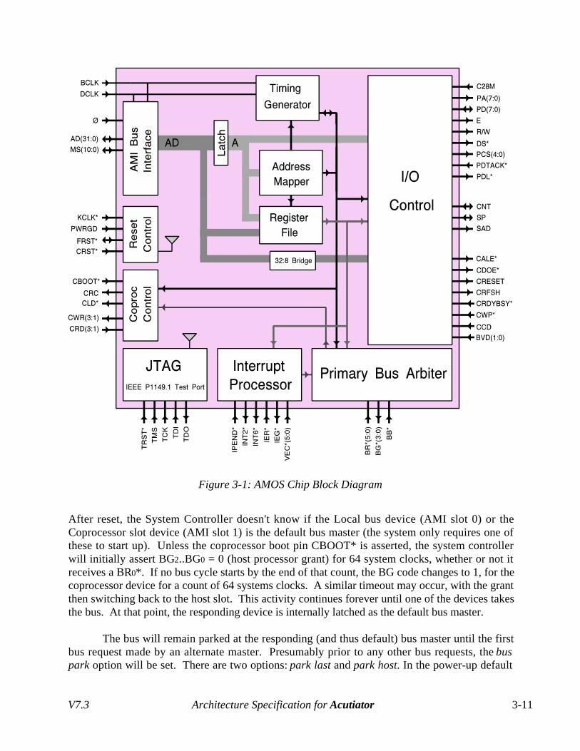
The actual AMOS design, while new in many areas, is the logical successor of parts of the Amiga 3000's Gary, RAMSEY, and Buster gate arrays. Based on the latest design methodologies, it doesn't make much sense to adapt actual logic from any of these parts, since most of the Acutiator chips will rely heavyily on logic synthesis, and must support clock speeds considerably beyond anything considered in the Amiga 3000 architecture. A block diagram of the AMOS chip is given in Figure 3-1.
3.9 MC68020/MC68030 Bus Support
The Acutiator bus attempts to support host processors that have bus access behavior similar to that of the MC68020/MC68040. This is reall just a matter of the specification of some small protocol variances to the MC68040 conventions. No other Acutiator chips will be affected by these protocols. The protocl changes really just pertain to the behavior of the Acutiator system at boot-up time. We have to make sure that the host processor gets enough time on the system bus to start the whole system going.
V7.3 Architecture Specification for Acutiator 3-11
After reset, the System Controller doesn't know if the Local bus device (AMI slot 0) or the Coprocessor slot device (AMI slot 1) is the default bus master (the system only requires one of these to start up). Unless the coprocessor boot pin CBOOT* is asserted, the system controller will initially assert BG2..BG0 = 0 (host processor grant) for 64 system clocks, whether or not it receives a BR0*. If no bus cycle starts by the end of that count, the BG code changes to 1, for the coprocessor device for a count of 64 systems clocks. A similar timeout may occur, with the grant then switching back to the host slot. This activity continues forever until one of the devices takes the bus. At that point, the responding device is internally latched as the default bus master.
The bus will remain parked at the responding (and thus default) bus master until the first bus request made by an alternate master. Presumably prior to any other bus requests, the bus park option will be set. There are two options: park last and park host. In the power-up default
Figure 3-1: AMOS Chip Block Diagram
Chapter 3: The Motherboard Controller V7.33-12
mode, park last, the bus will remain parked at the master last granted the bus until another request comes in. In park host mode, the bus mastership will automatically return to the system host whenever no other master is making a request. This takes place with or without a request from the host.
Previously the System Controller was responsible for responding to either MC68030 or MC68040 protocol interrupt acknowledge cycles. This is no longer the case, the AMI bus supports only the MC68040 protocol, where the T1-T0 code indicates interrupt acknowledge,
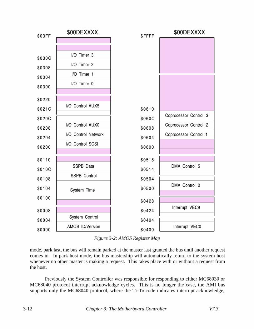
Figure 3-2: AMOS Register Map
V7.3 Architecture Specification for Acutiator 3-13
while the interrupt level is indicated on M2-M0. It's up to the CPU/RAM controller block to provide AMI bus compatible interrupt acknowledges and to provide any autovectoring signal that might be needed by the host processor.
3.10 RISC/Alternate Processor Bus Support
The AMI bus and System Controller, while generally designed to mesh nicely with MC68040 processor protocols, is designed to be reasonably processor independent. This is designed to allow easy support of coprocessors like the DSP3210, as well as future MC68060 or RISC host CPUs, on the bus. The basic protocols are easy to implement with m a handful of buffers and PALs from most modern CPU native bus interfaces. Registers are provided to taylor each bus master to the bus when its master. Some masters may support the full speed AMI bus with burst, others may only run single cycles.
The System Controller and AMI bus also support 64-bit processors. The 64-bit DRAM bus can be read as 64-bits wide, rather than a pipelined 32-bits wide. The AMI bus runs automatic double-32-bit transactions or octal-32-bit bursts in response to a 64-bit transaction request. See Chapter 7, “The AMI Bus”, for more information on this pseudo-64-bit protocol and other AMI bus issues.
3.11 Register Map
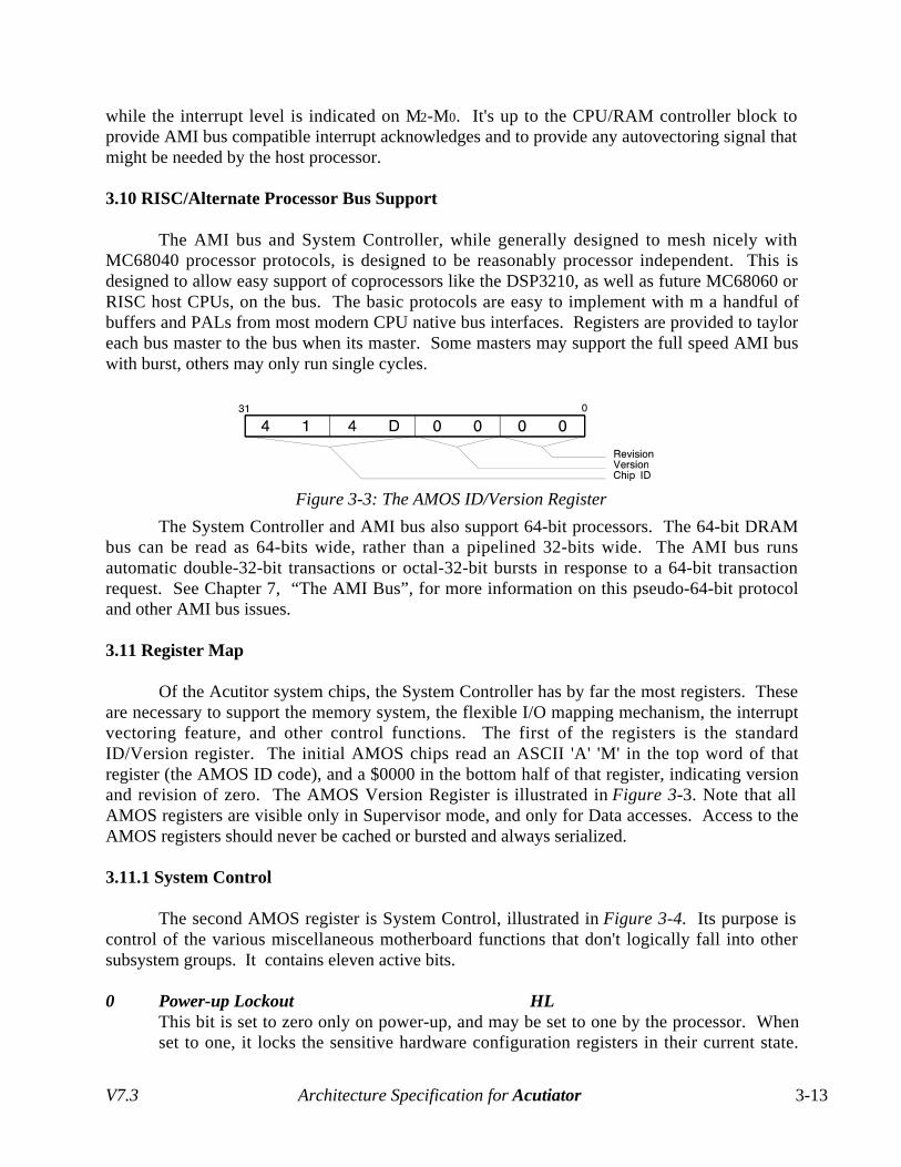
Of the Acutitor system chips, the System Controller has by far the most registers. These are necessary to support the memory system, the flexible I/O mapping mechanism, the interrupt vectoring feature, and other control functions. The first of the registers is the standard ID/Version register. The initial AMOS chips read an ASCII 'A' 'M' in the top word of that register (the AMOS ID code), and a $0000 in the bottom half of that register, indicating version and revision of zero. The AMOS Version Register is illustrated in Figure 3-3. Note that all AMOS registers are visible only in Supervisor mode, and only for Data accesses. Access to the AMOS registers should never be cached or bursted and always serialized.
3.11.1 System Control
The second AMOS register is System Control, illustrated in Figure 3-4. Its purpose is control of the various miscellaneous motherboard functions that don't logically fall into other subsystem groups. It contains eleven active bits.
0 Power-up Lockout HLThis bit is set to zero only on power-up, and may be set to one by the processor. When set to one, it locks the sensitive hardware configuration registers in their current state.
Figure 3-3: The AMOS ID/Version Register

Chapter 3: The Motherboard Controller V7.33-14
Figure 3-4: System Control Register
Bits/fields affected by this are indicted by “HL”. This bit also allows the OS to differentiate between cold and warm boots.
1 Keyboard Lockout SLThis bit controls keyboard reset. In its power-up setting of zero, the keyboard reset sequence will reset the system. If set to one by the processor, keyboard resets are ignored.
2 Soft Reset SLThis bit always reads as zero, but causes a simulated keyboard reset if written one. This allows the CPU to send a full-system reset to the system. A CPU-generated reset isn't the same, that's only an I/O reset.
4:3 Bus TimeoutThis is the Bus Timeout field. This register resets to zero, indicating that all cycles unterminated after approximately 8ms will be automatically given a normal termination. Writing a one here subquently causes unterminated cycles to be given an error acknowledge after approximately 250ms. Setting Bus Timeout to two causes all timeouts to be disabled, while a value of three is undefined.
5 Park Mode HLThis bit powers up zero, indicating that the host processor requests the bus, and thus it can remain parked at the last active master. If written one, the primary bus arbiter will assume the host doesn't actively request the bus, and so an unrequested bus returns to the host channel automatically.
10:7 Access LockThis register is a key to lock various fields against access by errant programs. The register resets to the unlocked state. A key written to it activates the soft lock, the inverted key written deactivates the soft lock. Affected fields are indicated by “SL”.
23:16 Retry Wait SLWhen a bus request from a DMA channel with Retry Enable set comes in, the controller will run a relinquish and retry cycle if the bus cycle doesn't complete within the number of clocks determined by the count in this field. No retry is attempted for channels with Retry Enable cleared or if this is set to zero.
28:30 Host Master Interrupt Priority SLThe host processor is generally fixed at a DMA priority of zero, other bus masters take on priority values relative to this. However, when an interrupt is taken, the master needs its priority bumped up; it gets bumped up to the value stored here.
31 Host Master Interrupt ResetThis bit is set to one when the system controller bumps host DMA priority up in response to an interrupt. A zero written here sets the priority back to zero.

V7.3 Architecture Specification for Acutiator 3-15
3.11.2 System Time Counter
This register pair is a 64-bit free running counter, starting at offset $0100. It counts BCLK cycles. To avoid rollover confusion, an access of the high-order register causes the count to freeze until the low-order register is accessed. A write to this register resets it to zero, which is also the value after a power-up reset.
3.11.3 SSPB Registers
The next two registers manage the Synchronous Serial Peripheral Bus, or SSPB. This is a flexible two/three-wire serial interface, designed to hook up to low cost serial bus I/O devices, such as those on the Philips I2C bus (two-wire) or ITT InterMetal bus (three-wire) protocols. It's expected that this will also support the emerging Access.Bus standard from DEC. The register at offset $010C is the SSPB data register, which transfers an eleven-bit serial stream in and out of AMOS onto the open-drain SP pin. The register at $0108 is the SSPB control register, which sets up clock and data options. There's an external data transition before the first clock, and one after the last clock. The SSPB Control bit field assignments are:
7:0 Clock SpeedThe SSPB automatic clock period is determined by the value written to the Clock Speed byte. The cycle time of CNT is given by (Clock Speed * 160ns), for values from 1 to 255. The value of Clock Speed is preserved over multiple SSPB data cycles.
8 Raw SP* This bit provides direct access to the SP line. A high written to Raw SP* will cause a
low on the SP line when the SSPB mechanism is not in a clocked transfer. A read of Raw SP* will return inverted the current state of the SP line. This allows the active programming of the SP line, to create unusual soft serial protocols.
9 Raw CNT* This bit provides direct access to the CNT line. A high written to Raw CNT* will cause
a low on the CNT line when the SSPB mechanism is not in a clocked transfer. A read of Raw CNT* will return inverted the current state of the CNT line. This allows the active programming of the CNT line.
10 Interrupt EnableThe Interrupt Enable bit is written low to disable interrupts, high to cause an INT2* interrupt to be generated by AMOS when a byte has been transferred over the SSPB bus.
Figure 3-5: SSPB Registers
Chapter 3: The Motherboard Controller V7.33-16
Interrupts are generally used by all clocked SSPB protocols, and they're normally autovectored; there doesn't currently seem to be any need for vectoring, though this remains an open issue until the Access.Bus specification is obtained.
11 Transfer CompleteThe Transfer Complete bit goes high to indicate that a successful transfer has completed; it is cleared on read, a no-op on write.
12 Serial ModeThis bit resets clear, indicating that a normal two or three wire cycle will be generated the next time data is written to the SSPB data register. Setting this bit causes the SAD line to be driven to indicate a 3-wire address cycle. It will automatically clear after the cycle is run.
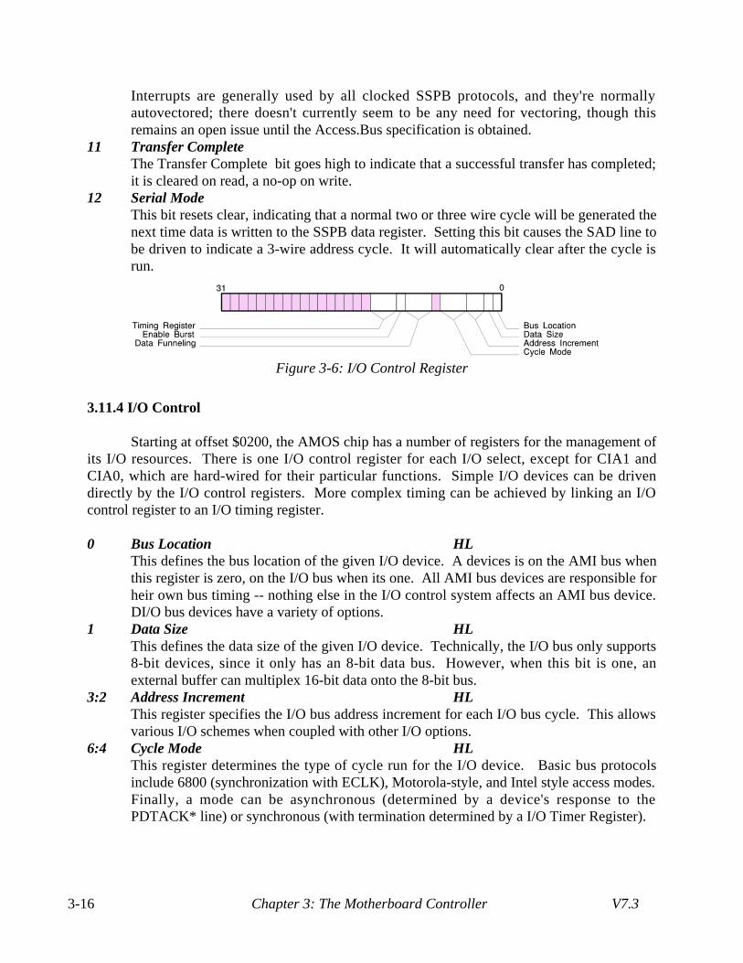
3.11.4 I/O Control
Starting at offset $0200, the AMOS chip has a number of registers for the management of its I/O resources. There is one I/O control register for each I/O select, except for CIA1 and CIA0, which are hard-wired for their particular functions. Simple I/O devices can be driven directly by the I/O control registers. More complex timing can be achieved by linking an I/O control register to an I/O timing register.
0 Bus Location HLThis defines the bus location of the given I/O device. A devices is on the AMI bus when this register is zero, on the I/O bus when its one. All AMI bus devices are responsible for heir own bus timing -- nothing else in the I/O control system affects an AMI bus device. DI/O bus devices have a variety of options.
1 Data Size HLThis defines the data size of the given I/O device. Technically, the I/O bus only supports 8-bit devices, since it only has an 8-bit data bus. However, when this bit is one, an external buffer can multiplex 16-bit data onto the 8-bit bus.
3:2 Address Increment HLThis register specifies the I/O bus address increment for each I/O bus cycle. This allows various I/O schemes when coupled with other I/O options.
6:4 Cycle Mode HLThis register determines the type of cycle run for the I/O device. Basic bus protocols include 6800 (synchronization with ECLK), Motorola-style, and Intel style access modes. Finally, a mode can be asynchronous (determined by a device's response to the PDTACK* line) or synchronous (with termination determined by a I/O Timer Register).
Figure 3-6: I/O Control Register
V7.3 Architecture Specification for Acutiator 3-17
Code Function0 No I/O for this channel1 6800-style cycle2 Mototola-style asynchronous cycle3 Intel-style asynchronous cycle4 Motorola-style synchronous cycle5 Intel-style synchronous cycle6 Motorola-style modified asynchronous cycle7 Intel-style modified asynchronous cycle
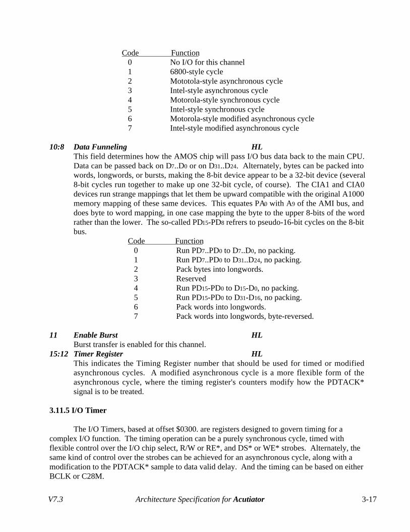
10:8 Data Funneling HLThis field determines how the AMOS chip will pass I/O bus data back to the main CPU. Data can be passed back on D7..D0 or on D31..D24. Alternately, bytes can be packed into words, longwords, or bursts, making the 8-bit device appear to be a 32-bit device (several 8-bit cycles run together to make up one 32-bit cycle, of course). The CIA1 and CIA0 devices run strange mappings that let them be upward compatible with the original A1000 memory mapping of these same devices. This equates PA0 with A9 of the AMI bus, and does byte to word mapping, in one case mapping the byte to the upper 8-bits of the word rather than the lower. The so-called PD15-PD8 refrers to pseudo-16-bit cycles on the 8-bit bus.
Code Function0 Run PD7..PD0 to D7..D0, no packing.1 Run PD7..PD0 to D31..D24, no packing.2 Pack bytes into longwords.3 Reserved4 Run PD15-PD0 to D15-D0, no packing.5 Run PD15-PD0 to D31-D16, no packing.6 Pack words into longwords.7 Pack words into longwords, byte-reversed.
11 Enable Burst HLBurst transfer is enabled for this channel.
15:12 Timer Register HLThis indicates the Timing Register number that should be used for timed or modified asynchronous cycles. A modified asynchronous cycle is a more flexible form of the asynchronous cycle, where the timing register's counters modify how the PDTACK* signal is to be treated.
3.11.5 I/O Timer
The I/O Timers, based at offset $0300. are registers designed to govern timing for a complex I/O function. The timing operation can be a purely synchronous cycle, timed with flexible control over the I/O chip select, R/W or RE*, and DS* or WE* strobes. Alternately, the same kind of control over the strobes can be achieved for an asynchronous cycle, along with a modification to the PDTACK* sample to data valid delay. And the timing can be based on either BCLK or C28M.

Chapter 3: The Motherboard Controller V7.33-18
1 Clock Source HLThis bit selects between the I/O clock, C28M, and the AMI bus clock, BCLK, for use as the timer's basis clock. The use of BCLK should allow the peripheral to run synchronously to the AMI bus, while C28M will always require synchronization. On the other hand, C28M is a fixed value, whereas BCLK will be different depending on system clock speeds.
12:8 Access Count HLFor synchronous cycles, this five bit field determines the number of clock cycles used for access, where the count is (Cycle Timing + 2). For asynchronous cycles, it determines the cycle count between PDTACK* received and data latched/cycle ended.
19:16 CS Delay HLThis field sets the count between peripheral address valid and CS/cycle start for the given I/O device.
23:20 DS Delay HLThis field sets the count between peripheral address valid and Data (Motorola mode) or Read-Write (Intel mode) strobe valid for the given I/O device.
27:24 Recovery HLThis field sets a minimum spacing between consecutive cycles one same device.
3.11.6 Interrupt Control
Starting at offset $0400, the AMOS chip has a number of registers for the management of interrupts. The register format is:
Figure 3-8: I/O Timing Effects
Figure 3-7: I/O Timer Register
V7.3 Architecture Specification for Acutiator 3-19
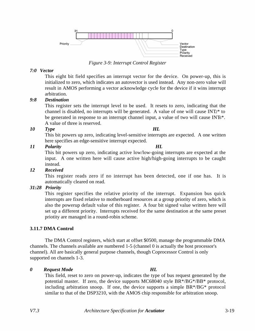
7:0 VectorThis eight bit field specifies an interrupt vector for the device. On power-up, this is initialized to zero, which indicates an autovector is used instead. Any non-zero value will result in AMOS performing a vector acknowledge cycle for the device if it wins interrupt arbitration.
9:8 DestinationThis register sets the interrupt level to be used. It resets to zero, indicating that the channel is disabled, no interrupts will be generated. A value of one will cause INT2* to be generated in response to an interrupt channel input, a value of two will cause INT6*. A value of three is reserved.
10 Type HLThis bit powers up zero, indicating level-sensitive interrupts are expected. A one written here specifies an edge-sensitive interrupt expected.
11 Polarity HLThis bit powers up zero, indicating active low/low-going interrupts are expected at the input. A one written here will cause active high/high-going interrupts to be caught instead.
12 ReceivedThis register reads zero if no interrupt has been detected, one if one has. It is automatically cleared on read.
31:28 PriorityThis register specifies the relative priority of the interrupt. Expansion bus quick interrupts are fixed relative to motherboard resources at a group priority of zero, which is also the powerup default value of this register. A four bit signed value written here will set up a different priority. Interrupts received for the same destination at the same preset priotity are managed in a round-robin scheme.
3.11.7 DMA Control
The DMA Control registers, which start at offset $0500, manage the programmable DMA channels. The channels available are numbered 1-5 (channel 0 is actually the host processor's channel). All are basically general purpose channels, though Coprocessor Control is only supported on channels 1-3.
0 Request Mode HLThis field, reset to zero on power-up, indicates the type of bus request generated by the potential master. If zero, the device supports MC68040 style BR*/BG*/BB* protocol, including arbitration snoop. If one, the device supports a simple BR*/BG* protocol similar to that of the DSP3210, with the AMOS chip responsible for arbitration snoop.
Figure 3-9: Interrupt Control Register

Chapter 3: The Motherboard Controller V7.33-20
1 Retry EnableThis bit conrols the system's relinquish and retry mechanism with respect to the given channel. In the reset condition of zero, no retry is used for the channel, while when set to one, the system retry wait regster is used to time out a retry when the channel's bus request is asserted.
2 Burst Enable SL This register indicates the burst capability of the potential bus master. When set to the
power-up value of zero, burst is not supported. When set to one, burst is supported. 10:8 Modifier Type
When set non-zero, this register supplies a value to be driven by the system controller for the M2-M0 lines, and also forces T1-T0 to be driven to “normal access” when this device is master. If zero, these lines are tri-state during the device's mastership.
16 Error FlagThis is set when a bus error is generated during the tenure of the specified bus master. It is cleared on reset or when rewritten.
19:17 Error CodeThis is the AMI bus error code that was present when an error caused the Error Flag bit to be set. In the case of multiple bus errors, the last error is stored here.
20 Access FlagThis is set when the potential master actually run a bus cycle. It is cleared on reset or when rewritten.
31:28 PriorityThis register specifies the relative priority of the DMA channel A four bit signed value written here will set up a priority, which defsults to zero. Requests received at the same preset priority are granted in a round-robin (eg, fair) scheme.
3.11.8 Coprocessor Control
The Coprocessor Control registers, based at $0600, are designed to allow the host processor to easily manage simple control of alternate processors. This isn't generally necessary for devices that are of the “DMA controller” nature (eg, SCSI, Ethernet, etc.), but it is generally necessary for devices that are of the “Coprocessor” nature (eg, DSP, CPU farm, etc.). The bits are as follows:
Figure 3-10: DMA Control Register
Figure 3-11: Coprocessor Control Register
V7.3 Architecture Specification for Acutiator 3-21
0:1 Input OptionsThis field specifies some modified behavior for the input data register. When set to zero. as on powerup, the input lines are simply port lines. When bit 0 is set, bit 0 of the input register causes an interrupt to be generated, based on the indicated vector register. When bit 1 is set, bit 1 of the input register acts as a negative edge detector rather than an indicator of the input level.
7:4 Vector RegisterThis register specifies an interrupt control register to use for generating any interrupt called for by the Input Mode setting. The trigger condition is set by the Input Mode setting, while the vector, level, and priority are based on this selected register number.
9:8 Output ModeThis field specified a modification to the output data register. If bit 0 is set, bit 0 of the output register acts as a negative-going strobe rather than a fixed port line. If bit 1 is set, bit 1 of the output register acts as a positive-going strobe rather than a fixed port line.
23:16 Input DataThis is the input data register. It generally reflects the status of the input data port, though its behavior can be somewhat modified by the Input Mode setting.
31:24 Output DataThis is the output data register. This is generally written to directly drive the output port lines, though its behavior can be modified somewhat by the Output Mode setting. The values written here can be read back at any time.
3.12 PCMCIA Registers
The Credit Card registers are mapped according to the standard PCMCIAconventions. Registers are provided to locate PCMCIA address and I/O in the system memory map. These mappings will be provided in a future release of this specification.
3.13 Memory Mapping
The AMOS chip does lots of memory mapping. The chip itself is located at a base of $00DE0000. The various resources it maps are:
Signal Range CIA0* $00BF0000 $00BFFFFFCIA1* $00BF0000 $00BFFFFFCIA2* $00BE0000 $00BFFFFFSCSI* $00DD0000 $00DDFFFFNET* $00D90000 $00D9FFFFAUX0* $00DB0000 $00DBFFFFAUX1* $00BD0000 $00DDFFFFAUX2* $00BC0000 $00BCFFFFAUX3* $00BB0000 $00BBFFFFAUX4* $00BA0000 $00BAFFFFMEM0* $04000000 $04FFFFFFMEM1* $05000000 $05FFFFFFMEM2* $06000000 $06FFFFFF

Chapter 3: The Motherboard Controller V7.33-22
MEM3* $07000000 $07FFFFFFPCMCIA Memory TBDPCMCIA I/O TBDPCMCIA Attribute TBD

V7.0 Architecture Specification for Acutiator 4-1
Chapter 4The Amiga Chip Controller
The Amiga Chip Controller is the interface between the Acutiator System Bus and the particulars of a given implementation of the Amiga Chips and Chip Bus. This device encapsulates the interface logic between any specific Amiga chip set and the rest of the Acutiator system. The particular Chip Controller specified here is designed to be a high performance interface between the AMI bus and the AAA Chip Bus, but a similar design could be done for any Amiga chip architecture.
Chip RAM access speed has been the one heretofore unsurmountable bottleneck in Amiga systems. The Chip Controller is designed to drastically reduce this bottleneck. It's very possible for this to be done with systems like AA or probably AA+, but AAA makes it especially simple. The Chip Controller contains a flexible data path FIFO, which sits between the AMI and RGA/D buses. This device can match CPU to Chip Bus speeds, write-buffer for zero wait write cycles, and lookahead in Chip RAM for more efficient block copies even when the AMI bus master isn't running burst cycles. The Chip Controller can interface to the AAA Chip bus either via the standard Andrea-controlled access or it can master the AAA DRAM bus and drive memory cycles itself at full CPU speed.
4.1The JTAG Test Port
As in all Acutiator chips, a test port for the IEEE P1149.1 boundary scan protocol is defined. While such a port isn't vital to the operation of the device, we're convinced that board-wide JTAG support will be useful for both Chip and System testing. The pin requirements are:
Signal(s) CountClock 1Mode Select 1Data 2Reset 1
TOTAL 5
The actual test register map will be defined based on the chip implementation, it doesn't belong in this architecture specification. However, we do expect any implementation will at the least support the normal boundary scan functions.
4.2 The AMI Bus Interface
Virtually all of the AMI bus signals go to the Chip Controller, though as a slave-only device, no arbitration signals are needed. It needs full address, data, and control in slave mode

Chapter 4: The Amiga Chip Controller V7.04-2
during AMI bus to Chip bus conversions. Additionally, the AMI bus basis clock provides synchronization for all AMI bus events and various internal operations. The initial pin count estimate for this subsection is:
Signal(s) CountClocks 2Adresss/Data Bus 32Master/Slave Bus 11Additional Control 1
TOTAL 46
AMI Bus Signals
BCLK AMI bus basis clock. All AMI bus signal transitions are references to this clock.
Ø AMI bus phase clock. This clock determines the multiplexing of the address/data and master/slave signals on the AMI bus.
AD31-AD0 AMI bus address/data signals.MS10-MS0 AMI bus control signals.CRST* CPU Reset strobe.
4.3 The Chip Bus Interface
The Amiga Chip Controller device interfaces directly to the AAA system's Andrea chip. Most Chip bus related timing comes from the Andrea basis and bus clocks, while all Chip bus activity is initiated by activating this control interface. The list of signals is as follows:
Signal(s) CountChip Bus Clocks 2A/D Bus 32Chip Bus Controls 6
TOTAL 40
Chip Bus Clocks
MCLK Chip bus basis clock.BUSCLK Chip bus transaction clock.
A/D Bus
RA/D31-RA/D0 This is the AAA multiplexed address/data bus. Transfers between the Chjp bus and the AMI bus are buffered though the Chip Controller in a variety of ways depending on the exact transfer mode and cycle type in question.

V7.0 Architecture Specification for Acutiator 4-3
Chip Bus Controls
ALE* Address Latch Enable. This bidirectional chip bus signal determines when Chip bus addresses are latched.
LATCH* Data Latch. This bidirectional chip bus signal determines when data is latched from the chip bus into the Chip Controller device.
AS* This is the Andrea address strobe. This and the NEED* signal are driven to cause a normal Andrea access.
RAM/REG* This strobe is driven by the Chip controller logic to tell Andrea if the current cycle is for Andrea registers or for Chip RAM. Note that some register accesses involve 16 to 32 bit bus sizing, and all are burst and cache inhibited.
DUAL/SING* This line determines if the Chip bus is for a dual or single system. This impacts a few of the interface decisions.
ARST* Andrea Reset. This line resets Andrea under control of the Chip Controller's reset register. This lets any DRAM/VRAM configuration codes can be entered before Andrea is reset, and ensures a 10ms reset pulse on powerup.
4.4 The Chip Bus Arbiter
The Chip bus arbiter manages the access of the chip bus by the AMI bus master. The Andrea chip supports two kinds of bus mastership, either Andrea-controller or externally controlled. For Andrea controlled cycles, Andrea is responsible for providing chip bus DRAM timing, while the AMI bus master must somehow synch up or down to that cycle. The Chip Controller handles this type of cycle by running data through a FIFO, so a full speed Chip bus cycle can be run, even with burst, without intra-cycle synchronization delays. The Chip Controller also supports the externally controller Chip RAM cycle, where is must drive all DRAM signals itself. The advantage of this type cycle is that the DRAM cycle is run synchronous to the AMI bus clock rather than the Chip bus clock, so it's more efficient. The required signals for this group are:
Signal(s) CountNormal Access 2External Access 2Holdoff 1
TOTAL 5
Chip Bus Arbiter Signals
NEED* This is asserted by the Chip Controller for normal Chip bus access. All register accesses and Andrea-controller DRAM accesses are activated when the Chip Controller asserts NEED* and AS* appropriately. The Andrea chip manages the synchronization of NEED* to the Chip bus clock.
BG* This signal is asserted by Andrea to grant one standard cycle to the Chip Controller. This may be a single or burst cycle, depending on the state of the burst request (only used for DRAM access).

Chapter 4: The Amiga Chip Controller V7.04-4
HIGHRQ* This signal is asserted by the Chip Controller for a high priority access to the Chip DRAM bus. In this mode, the controller drives all the DRAM signals.
HIGHBG* This signal is asserted by Andrea to give the Chip Controller the go-ahead to master the Chip DRAM bus.
GOAWAY* This signal is asserted by Andrea to indicate to the Chip Controller that the next Chip bus cycle cannot be granted to the AMI bus master. This can optionally cause the Chip Controller to issue a retry termination on the AMI bus rather than stall out waiting for Chip bus access.
4.5 The Chip RAM Interface
Timing of the Chip bus is managed by either the Andrea Chip or the Chip Controller, depending on the bus access mode granted by Andrea. Not only does the Chip Controller manage DRAM controls for Andrea's “high priority” control mode, but it drives configuration codes for the DRAM/VRAM installed, based on some programmable registers. This interface is clever enough to support variable sized memory modules, by shifting the output RAS* controls appropriately. While the AAA timing to Chip RAM is basically fixed, the Chip Controller allows the DRAM access to be quite flexible when driven under its control. To take full advantage of this mode, memory timing registers must be programmed based on AMI bus speed and the type of DRAM installed. The Chip RAM Control Signals are:
Signal(s) CountAddress 14Memory Strobes 26Control 5
TOTAL 45
Address
MA 9-MA 0 This is the address bus for VRAM/DRAM addressing. MA8 is only used for parts addressed as 4MB devices. This is always driven by the current Chip RAM bus master.
XA3-XA0 This is the bank address bus, providing the selection of one out of eight possible banks for VRAM or DRAM. Note that the XA encoding depends on whether the system is dual or single for both DRAM and VRAM access.
Memory Strobes
RAS* This is the global Row Address Strobe. This is asserted by Andrea when mastering the DRAM bus to select the appropriate bank-specific RASN* strobe.
BRAS* This is the Row Address Strobe for external blitter cycles. These are generated by Andrea for satellite blitter chips, which are supported by Andrea but don't currently exist.

V7.0 Architecture Specification for Acutiator 4-5
RAS7*-RAS0* These are the bank-specific Row Address Strobes. The XA3-XA 0 bus determines which of these will be driven for an Andrea-mastered DRAM cycle. When the Chip Controller is mastering the Chip bus, the bank is internally determined based on the bus address.
SE7*-SE0* These are the bank-specific serial port enable strobes. The XA3-XA0 bus determines which of these is driven for a VRAM serial cycle. The SEEN* line determines when the XA bus code is for VRAM cycles.
CAS7*-CAS0* These are the Column Address Strobes. They're driven by the current Chip bus controller. CAS7*-CAS4* correspond to CASH3*-CASH0*, the strobes for low-end systems and even longwords in high-end systems, while CAS3*-CAS0* correspond to CASL3*-CASL0*, the strobes for odd longwords in high-end systems.
Control
WE* This is the write enable strobe. This is driven by the current Chip bus master.RFSH This signal is driven by Andrea to indicate that a refresh cycle is taking place. SEEN* This line is driven by Andrea to enable one of the SEN* outputs.LATCHSE This line is asserted by Andrea to cause the current XA3-XA0 address to be
latched to select one of the eight SEN* outputs.
4.6 Special Functions
The chip controller have a couple of special functions designed to optimize the System to Amiga chip interface. As mentioned, the controller has a read/write FIFO that can also be used as a prefetch buffer. This allows transfers between Chip RAM and other RAM to go fast, even when burst transfers aren't possible. The direction of prefetch can be set for increment or decrement, allowing transfers to go either way. It also allows all writes to be buffered, so they run in zero wait states until the FIFO is full. Note that chip register access will always cause the read FIFO to be invalidated or the write FIFO to be flushed before access, and that chip register access does not get buffered or prefetched.
Two conversion functions are also supported. The first of these provides a mechanism for efficient chunky pixel to bitplane conversion, based around 8-bit chunky pixels. The other provides an efficient mechanism for certain kinds of bitplane to chunky pixel masking and conversion. Doing this in hardware is relatively simple and will speed up software considerably.
4.7 Amiga Chip Controller Summary
The chip controller specification, as presented here so far, considers the signals necessary to implement controllers for an AAA Chip subsystem. The support of zero wait writes, high speed burst transfers, and full speed DRAM cycle on the Chip RAM bus make this a major improvement in the Amiga system architecture, all but eliminating the Chip bus bottleneck except in very high bandwidth modes. Other Amiga Chip architectures, such as “AA” or “AA+” will define a different Chip Controller. The current signal summaries are:

Chapter 4: The Amiga Chip Controller V7.04-6
Signal Group CountJTAG Interface 5AMI Bus Interface 46Chip Bus Interface 48Chip Bus Arbiter 5Chip RAM Interface 45
GRAND TOTAL 141
4.8 Notes on SAIL History
Since the Acutiator project was started considerably before any serious systems work was done with the AAA chip set, a good bit of consideration was given to dealing with the AA chip set. Unlike AAA, the AA design is pretty unflexible, designed to sit on a 68000 or 68030 bus with a little bit of work. AA has all the mapping and bus conversion requirements of AAA, but it adds some extra concerns.
The main concern of the AA system on a high-end or even med-range Amiga computer is its video bus saturation at even relatively uninteresting display resolutions. In order to get around this problem, a two-chip solution was proposed for gluing AA into Acutiator systems. The first of these chips was a SAIL controller for AA. This was analogous to the AAA SAIL: it provided memory mapping, bus conversion control, memory control, etc. This is more difficult for AA, since there is no way to directly take control of the memory control signals, they must be externally tri-stated or processed through the AA SAIL. In any case, it could be done.
The interesting part of the AA SAIL implementation is the second chip, MOBI, a complex data path interface device that would act under the direction of the AA SAIL. This part, together with SAIL, managed a 64-bit RAM bus, a 32-bit AMI bus, and a 32-bit Chip bus. The two halves of the RAM bus would appear interleaved from the bitplane access point of view, so that, even in high video saturation modes, video fetch would be out of the way of CPU access very quickly. This allowed a fully saturated AA system to offer nearly full bandwidth to the host CPU. Additionally, the Chip RAM prefetch buffering mechanism, retained in the AAA SAIL chip, could boost this performance to nearly twice the A3000/A4000 level of performance for linear accesses, even with full video saturation occurring.
The 64-bit RAM bus is a bit of overkill for an AAA implementation of SAIL, especially since such a design can't be done in a single controller chip. The video RAM of AAA achieves much the same effect, by removing video contention from the main RAM bus. However, such a design may be interesting to consider for other chip set interfaces, and may even be a thing to consider as a built-in feature for future Amiga chip sets (of course, plenty of new features, such as a native AMI bus interface, should be considered for future Amiga Chips assuming Acutiator as specified here becomes a reality).

V7.0 Architecture Specification for Acutiator 4-7
4.9 The “AAA” SAIL Chip
The Synchronous Amiga Interface with Latch device, SAIL, is a single Chip implementation of the Amiga Chip Controller for use with the AAA Chip bus subsystem defined by the Andrea Chip. A diagram of this is shown in Figure 4-1. This is to be built as a 160 pin PQFP in 0.8um CMOS. The basic 141 pins for Amiga Chip Controller signals, plus four VDD pins and six VSS pins comes to a total of 151 pins, leaving nine spares.
4.10 Register Mapping
The mapping of SAIL registers is shown in Figure 4-2. These 32-bit registers reside at the fixed SAIL address, $00DC0000. These registers control the translation of AMI bus to Chip bus cycles, the interface used to access Chip RAM, various speed controls over Chip RAM mastered with the AAA “high-priority” interface, and some pixel type conversion functions. Additionally, some control over the location of the Chip bus facilities is provided, so this part can easily be used in non-standard applications (eg, AAA Zorro cards rather than modules or motherboards, etc.).
Figure 4-1: The AAA SAIL Chip
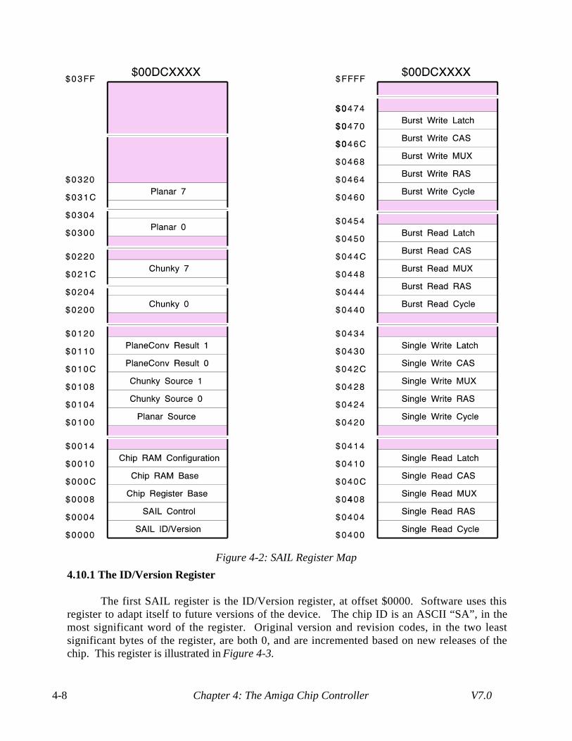
Chapter 4: The Amiga Chip Controller V7.04-8
4.10.1 The ID/Version Register
The first SAIL register is the ID/Version register, at offset $0000. Software uses this register to adapt itself to future versions of the device. The chip ID is an ASCII “SA”, in the most significant word of the register. Original version and revision codes, in the two least significant bytes of the register, are both 0, and are incremented based on new releases of the chip. This register is illustrated in Figure 4-3.
Figure 4-2: SAIL Register Map
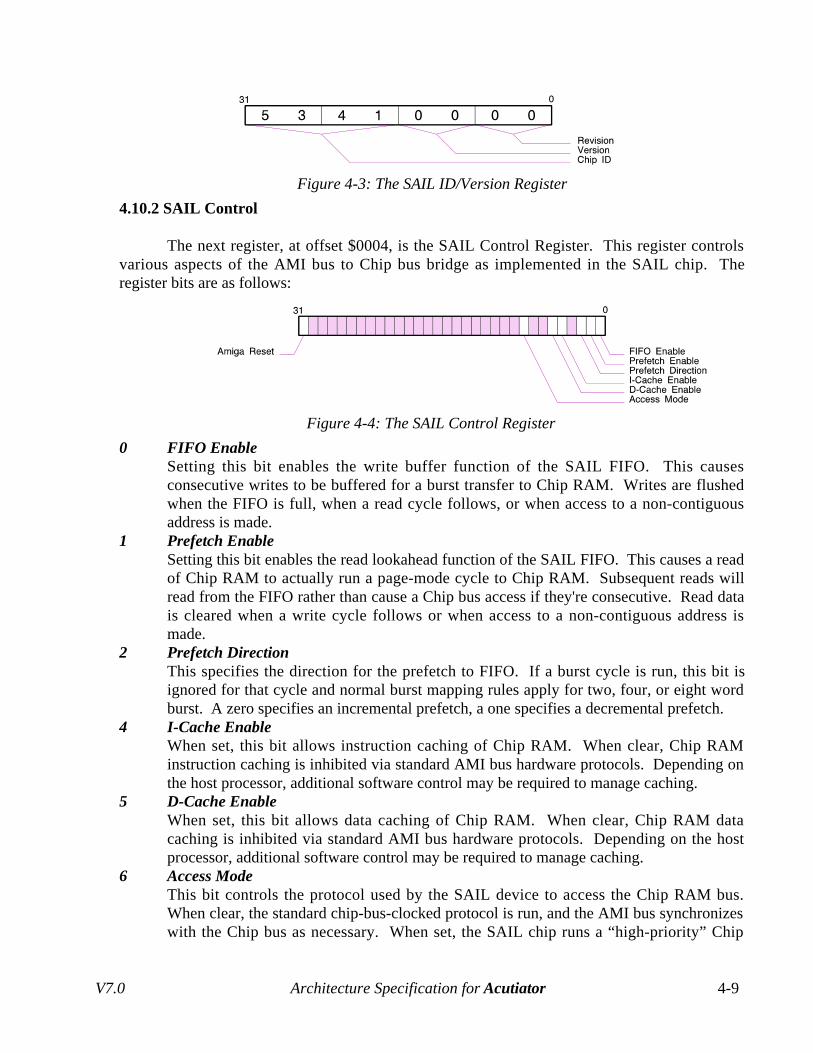
V7.0 Architecture Specification for Acutiator 4-9
4.10.2 SAIL Control
The next register, at offset $0004, is the SAIL Control Register. This register controls various aspects of the AMI bus to Chip bus bridge as implemented in the SAIL chip. The register bits are as follows:
0 FIFO EnableSetting this bit enables the write buffer function of the SAIL FIFO. This causes consecutive writes to be buffered for a burst transfer to Chip RAM. Writes are flushed when the FIFO is full, when a read cycle follows, or when access to a non-contiguous address is made.
1 Prefetch EnableSetting this bit enables the read lookahead function of the SAIL FIFO. This causes a read of Chip RAM to actually run a page-mode cycle to Chip RAM. Subsequent reads will read from the FIFO rather than cause a Chip bus access if they're consecutive. Read data is cleared when a write cycle follows or when access to a non-contiguous address is made.
2 Prefetch DirectionThis specifies the direction for the prefetch to FIFO. If a burst cycle is run, this bit is ignored for that cycle and normal burst mapping rules apply for two, four, or eight word burst. A zero specifies an incremental prefetch, a one specifies a decremental prefetch.
4 I-Cache EnableWhen set, this bit allows instruction caching of Chip RAM. When clear, Chip RAM instruction caching is inhibited via standard AMI bus hardware protocols. Depending on the host processor, additional software control may be required to manage caching.
5 D-Cache EnableWhen set, this bit allows data caching of Chip RAM. When clear, Chip RAM data caching is inhibited via standard AMI bus hardware protocols. Depending on the host processor, additional software control may be required to manage caching.
6 Access ModeThis bit controls the protocol used by the SAIL device to access the Chip RAM bus. When clear, the standard chip-bus-clocked protocol is run, and the AMI bus synchronizes with the Chip bus as necessary. When set, the SAIL chip runs a “high-priority” Chip
Figure 4-3: The SAIL ID/Version Register
Figure 4-4: The SAIL Control Register
Chapter 4: The Amiga Chip Controller V7.04-10
RAM access, where it drives the Chip bus signals synchronously to the AMI bus clocks. The timing for this is based on the RAM Timing Register sets described later in this chapter.
31 Amiga ResetThis bit provides software-controllable reset over the Amiga chips. It powers up low, indicating the reset condition. Several registers here are generally initialized by the host CPU before setting this bit high and allowing the Amiga chips to start up.
4.10.3 Chip Register Base
This register, at offset $0008, is the base address of the 64K space defined for “AAA” Chip registers. This register powers up defaulting to $00DF0000, but may be changed to any natural 64K boundary by the controlling CPU. Among other things, this makes it easy for the SAIL chip to act as a controller for Zorro card implementations of the “AAA” chip subsystem.
4.10.4 Chip RAM Base
This register, at offset $000C, is the base address of the 16MB space defined for “AAA” Chip RAM. Prior to the initialization of this register, Chip RAM is available only at the original 2MB space starting at $00000000. Current Acutiator specifications call for extended Chip RAM to be located based at $01000000, but this relocation mechanism allows Chip RAM to be located at any natural 16MB boundary.
4.10.5 Chip RAM Configuration
This register is initialized to the basic configuration codes to be sent to the “AAA” chipset in response to a Chip RAM configuration cycle. However, the SAIL chip can resolve holes in the bank-map of the Chip RAM, allowing much easier support of SIMM-based systems. Software writes the actual bank settings here, the SAIL chip generates the bank-contiguous version for the configuration cycle.
The format of this is just like that of the RAMATTR register in Andrea. There are eight logical banks of RAM, where bank N is represented by nybble D(N*4+3)-D(N*4). The meaning of each bit in the nybble is as follows:
Bit Name Meaning3 Slot filled This is low when filled, high when empty.2 RAM size This is low for RAM with 9 address lines, high for RAM with 10.1 BLIT chip This is set high to indicate a satellite blitter exists for this bank.0 RAM type This is set low for page-mode RAM, high for VRAM.
The SAIL chip doesn't mandate the mechanism for determining the type of RAM used in the system. A memory module-based machine may use ID codes like the “Nyx” prototype system, which allow SIMM-like modules to be used for upgrades. A board with a fixed memory arrary may have software poll RAM or initialize it from ROM, based on any memory type constraints the board may add.
V7.0 Architecture Specification for Acutiator 4-11
4.10.6 The Plane Conversion Mechanism
The next five registers support a mechanism for converting a bit planar image to a series of 8-bit chunky pixels. This can be used for efficient mask conversions and other such functions. The first register is the Planar Source register. The least significant byte here accepts a byte of bitplane data and starts the conversion process. Bits 7-0 in this register correspond directly to bytes 7-0 in the 64-bit register at offset $0110. When a bit in the Planar Source register is 0, the corresponding byte is loaded from the least significant byte of the Chunky Source 0 register at $0104. Similarly, when a bit in the Planar Source register is 1, the corresponding byte is loaded from the least significant byte of the Chunky Source 1 register at $108.
4.10.7 The Data Conversion Table
The next set of registers contains two separate 32-byte tables, for the conversion between chunky and planar data. The chunky table represents 32 consecutive 8-bit chunky pixels, while the planar table represents 32-bits each of the the corresponding 8 bitplanes. The conversion matrix is as follows. The chunky table looks like this:
$0200 P0,7 ... P0,0 P1,7 ... P1,0 P2,7 ... P2,0 P3,7 ... P3,0
$0204 P4,7 ... P4,0 P5,7 ... P5,0 P6,7 ... P6,0 P7,7 ... P7,0
$0208 P8,7 ... P8,0 P9,7 ... P9,0 P10,7 ... P10,0 P11,7 ... P11,0
$020C P12,7 ... P12,0 P13,7 ... P13,0 P14,7 ... P14,0 P15,7 ... P15,0
$0210 P16,7 ... P16,0 P17,7 ... P17,0 P18,7 ... P18,0 P19,7 ... P19,0
$0214 P20,7 ... P20,0 P21,7 ... P21,0 P22,7 ... P22,0 P23,7 ... P23,0
$0218 P24,7 ... P24,0 P25,7 ... P25,0 P26,7 ... P26,0 P27,7 ... P27,0
$021C P28,7 ... P28,0 P29,7 ... P29,0 P30,7 ... P30,0 P31,7 ... P31,0
The planar table looks like this:
$0218 P24,7 ... P24,0 P25,7 ... P25,0 P26,7 ... P26,0 P27,7 ... P27,0
$0300 P0,0 ... P7,0 P8,0 ... P15,0 P16,0 ... P23,0 P24,0 ... P31,0
$0304 P0,1 ... P7,1 P8,1 ... P15,1 P16,1 ... P23,1 P24,1 ... P31,1
$0308 P0,2 ... P7,2 P8,2 ... P15,2 P16,2 ... P23,2 P24,2 ... P31,2
$030C P0,3 ... P7,3 P8,3 ... P15,3 P16,3 ... P23,3 P24,3 ... P31,3
$0310 P0,4 ... P7,4 P8,4 ... P15,4 P16,4 ... P23,4 P24,4 ... P31,4
$0314 P0,5 ... P7,5 P8,5 ... P15,5 P16,5 ... P23,5 P24,5 ... P31,5
$0318 P0,6 ... P7,6 P8,6 ... P15,6 P16,6 ... P23,6 P24,6 ... P31,6
$031C P0,7 ... P7,7 P8,7 ... P15,7 P16,7 ... P23,7 P24,7 ... P31,7
Both tables are read/write, basically accessing the same data in different ways. They're organized to allow CPU bursts from 32 or 64-bit processors, as well as multi-byte moves. Since the size of the table and conversion is fixed, this can be implemented as a simple hardwired matrix rather than a shifting mechanism. Therefore, all conversions are instantaneous, the conversion is bidirectional, and there's no requirement in the machinery to convert a certain number of pixels before anything can be done with them.

Chapter 4: The Amiga Chip Controller V7.04-12
4.10.8 Chip RAM Timing
There are four sets of five registers each devoted to the control of Chip RAM timing during “high-priority” Chip bus accesses. The sets are at $0400 for single-beat reads, $0420 for single-beat writes, $0440 for burst reads, and $0460 for burst writes. Each RAM timing group consists of four waveform registers and a counter. The cycle counter determines the total number of clocks used for the DRAM cycle, which can't exceed limits imposed by the Chip bus interface. The waveform registers drive RAS*, address MUX, CAS*, and latch control based on this cycle count.
4.11 Decode Mapping
The SAIL chip provides mapping for Chip RAM and Chip registers. The first two megabytes of Chip RAM runs from $00000000-$001FFFFF. This same two megabytes is repeated with the rest of Chip RAM in the programmable range, which is by current conventions set to $01000000-$01FFFFFF. Chip registers are located starting at $00DFF000 by default, but can be realigned to any 64K boundary as mentioned. The range $00DFF000-$00DFF1FF is mapped as 16-bit space, with proper word to longword funneling done. The rest is 32-bit register space. Finally, the SAIL chip's registers are based at $00DC0000.
V7.1 Architecture Specification for Acutiator 5-1
Chapter 5The Expansion Controller
Standard Amiga system expansion is managed in Acutiator machines by the Expansion Controller chip. Its purpose is to convert AMI bus cycles into Zorro bus cycles, Zorro cycles into AMI bus cycles, and manages expansion bus arbitration. It is designed to be completely self-contained, relying only on the AMI bus, a 28MHz clock input, and a few external buffers for support of the bus reset signals. This makes it independent of the Chip Bus architecture. This chip works something like the Level II Buster for the Amiga 3000 systems, though it manages all address, data, and control paths between the buses. The data path incorporates a write buffer, which acts as a write latch for Zorro II bus cycles and as a burst FIFO for Zorro III cycles. The chip also incorporates a DMA controller for high speed bus to bus transfers.
When the AMI bus is acting as bus master, address decoding decides between Zorro II and Zorro III modes of operation. In most respects, the Expansion Controller support of Zorro II works like that of Fat Buster. Caching is mapped as in the Amiga 3000, according to the Zorro II rules first defined for the A2630 system. The Expansion Controller of course manages both address and data paths, and will latch Zorro II data on writes. For uncached burst writes, an entire line is buffered, and data bus bridging for 32 to 16 bit is managed. Behavior under Zorro III is similar, except that caching is permitted according to the Zorro III bus cache control line. In Zorro III mode, AMI bus burst cycles are converted to Zorro III multiple transfer cycles. The FIFO serves to improve the efficiency of this, as the entire burst transfer can be timed based on the specifics of each bus, rather than the current Amiga 3000 design, which incurs a full synch-down penalty after each word transferred.
If, during any AMI Bus to Zorro bus translation, two Zorro PICs collide, the cycle is terminated immediately. The Zorro data bus is tristated, the BERR* signal is driven on the Zorro bus, and the ET* and Collision Error code are driven on the AMI Bus. Other sources of BERR* on the Zorro bus result in ET* and the Unspecified Expansion Error code are driven on the AMI bus. ET* on the AMI bus doesn't normally result in BERR* being driven on the Expansion Bus.
When the Zorro bus becomes master, the Expansion Controller serves to translate Zorro cycles into the appropriate AMI bus cycle. For Zorro II masters, this involves a data bus bridge on odd-word cycles, as the 16-bit Zorro II device accesses 32-bit System Bus resources. For Zorro II devices, this is a simple bus to bus conversion, with write latching supported. The Expansion Controller does not do Zorro III to System Bus burst conversions. This kind of conversion is aways inefficient, since all of the Zorro III cycles must be monitored before any determination can be made as to whether or not the subcycles reside in the same quadlongword. The write latching does improve performance, though, as it tends to make the bus transfers somewhat pipelined, hiding the synch-down time normally associated with this kind of transfer. Additionally, all AMI bus resources are mapped as uncachable to Zorro III bus masters, at least for the moment. It will be necessary to implement the Zorro III multiprocessing extensions with
Chapter 5: The Expansion Controller V7.15-2
bus snooping, and snooping translations to the AMI bus, before a Zorro III device can safely cache any AMI bus resources.
The Expansion Controller fully supports Zorro III quick interrupt cycles. When it gets a response to a vector polling cycle, it will request the use of that interrupt via the IR* line. If the Motherboard Controller grants the interrupt for that cycle, IG* is returned immediately (the Motherboard Controller decides whether it requires the interrupt very quickly, so by the time polling is complete, the decision has been made). If not, the cycle is terminated without a vector phase; the responding devices will get their chance again during the next interrupt response cycle.
The Expansion Controller may ultimately support the Zorro III directed interrupt extensions, though they are not presently called for by this specification. Full support of directed interrupts would allow a Zorro III device to signal the DSP3210 or other coprocessor directly, rather than routing such signals though the host processor as is currently the requirement. Another possible extension is to provide interrupt vector registers for slow Zorro bus interrupts, much as the Motherboard Controller does for motherboard I/O.
Another function of the Expansion Controller is bus arbitration. It discriminates between Zorro II and Zorro III requests by sampling on the C7M clock. Software can assign prorities between Zorro II or Zorro III masters, but Zorro III requests have strict priority over Zorro II requests. Either request will result in a standard AMI bus request cycle being run to the AMI bus arbiter.
The final Expansion Controller function is the DMA controller. This mechanism permits transfers to be managed very efficiently between the AMI bus and the expansion bus (or, for that matter, transfers across either bus). This controller supports a flexible transfer scheme that allows it to service a linked list of in-memory transfer jobs before requiring intervention from the host processor. Intervention is signalled via an interrupt, which can be vectored in hardware or software and prioritized with respect to the other expansion interrupts. Optionally, this interrupt can be run to an interrupt channel of the System Controller and handled at the system priority level rather than the expansion priority level.
5.1 The JTAG Test Port
As in all Acutiator chips, a test port for the IEEE P1149.1 boundary scan protocol is defined. While such a port isn't vital to the operation of the device, we're convinced that board-wide JTAG support will be useful for both Chip and System testing. The pin requirements are:
Signal(s) CountClock 1Mode Select 1Data 2Reset 1
TOTAL 5

V7.1 Architecture Specification for Acutiator 5-3
The actual test register map will be defined based on the chip implementation, it doesn't belong in this architecture specification. However, we do expect any implementation will at the least support the normal boundary scan functions.
5.2 The Clocks
A minimum number of input clocks on the Expansion Controller manages to keep the requirements independent of anything but motherboard basis clocks. The single 28MHz video basis clock is used to generate required expansion bus clocks and synchronization to the Zorro II bus. Other clocks are detailed as part of the AMI bus interface. The pin count is:
Signal(s) CountInput clocks 2Output clocks 5
TOTAL 7
Input Clock
C28M 28MHz Zorro II basis clock.
Output Clocks
C1* Bus clock, 3.55MHz-3.58MHz.C3* Bus clock, 3.55MHz-3.58MHz, 90° behind C3*.C7M Bus clock, 7.09MHz-7.16MHz.CDAC Bus clock, 7.09MHz-7.16MHz, 90° behind C7M.E Bus clock, 709kHz-716kHz, 40%/60% duty cycle.
5.3 The AMI Bus Interface
Virtually all of the AMI bus signals go to the Expansion Controller. It needs full address, data, and control in slave mode during AMI bus to Zorro bus conversions, and address, data, and control in master mode during Zorro to AMI bus conversion. Additionally, the AMI bus basis clock provides synchronization for all AMI bus events. The initial pin count estimate for this subsection is:
Signal(s) CountClocks 3Adresss/Data Bus 32Master/Slave Bus 11Additional Control 2Interrupt 1
TOTAL 49
Chapter 5: The Expansion Controller V7.15-4
AMI Bus Signals
BCLK AMI bus basis clock. All AMI bus signal transitions are references to this clock.
DCLK Double-speed AMI bus clock.Ø AMI bus phase clock. This clock determines the multiplexing of the AMI bus.AD31-AD0 AMI bus address/data signals.MS10-MS0 AMI bus control signals.FRST* Full System reset strobe.CRST* CPU Reset strobe.INT* Open-drain, active low interrupt output.
5.4 Host Arbitration Signals
This group consists of signals used to obtain resources from the host processor bus. There are two resources that must be requested by the Expansion Controller: the right of mastership of the System Bus and the right of response to a particular interrupt. The signals required are counted:
Signal(s) CountBus Arbitration 3Interrupt Arbitration 2
TOTAL 5Bus Arbitration
BR* Bus request, asserted by EPIC when it requires the AMI bus.BG* Bus grant, asserted to EPIC indicating that it may master the AMI bus.BB* Bus busy, asserted by EPIC while mastering the AMI bus.
Interrupt Arbitration
IR* Interrupt request, asserted in response to a quick interrupt request cycle.IG* A grant indicating that the Expansion Controller may continue interrupt
service with a vector cycle.
5.5 The Zorro Bus Interface
Most of the Zorro bus signals go to the EPIC chip. The Zorro equivalents of every AMI Bus signal must go here, along with signals specific to the Zorro bus itself. The EPIC chip needs to act as a Zorro bus master when the Zorro bus is being mastered by the AMI bus or the DMA controller. Going the other direction, the EPIC chip needs to make the AMI bus look like a Zorro bus slave when a Zorro bus master accesses an AMI bus resource. The signals required for this are:

V7.1 Architecture Specification for Acutiator 5-5
Signal(s) CountMultiplexed A/D Bus 24Static Address/Data 14Control 19
TOTAL 57
This represents a full set of Zorro signals. The only additional pin requirements would be for enhancements of the current Zorro III specifiction, such as support of the directed interrupt or cache coherency extensions, which aren't currently planned for in Acutiator. Please refer to The Zorro III Bus Specification for more details on Zorro bus signals.
Address/Data
EAD31-EAD8 Multiplexed address/data bus, which forms part of the Zorro II mode non-multiplexed address and data buses.
EA7-EA2 Non-multiplexed address bus.ED7-ED0 Non-multiplexed data bus.
Control
LOCK* Bus lock signal in Zorro III mode, A1 in Zorro II mode.EDS3*-EDS0* Data byte strobes.FC2-FC0 Function codes, indicate processor address space type.FCS* Zorro III mode full cycle strobe.CCS* Zorro II cycle strobe.READ Data direction strobe.MTCR* Zorro III mode multiple transfer cycle clock, Zorro II mode DTACK* delay
strobe.MTACK* Zorro III mode multiple transfer cycle slave acknowledge.DTACK* Data transfer acknowledge.CINH* Cache inhibit strobe in Zorro III mode, DTACK* override in Zorro II mode.DOE Data buffer enable strobe.BERR* Bus error acknowledge.ERST* Main bus reset signal.EHLT* Bus halt signal. When asserted with ERST*, this indicates a full system reset
rather than a simple I/O reset.
5.6 Zorro Master/Slave Control
The final set of Expansion Controller signals is for the management of Zorro bus master and slave devices. Each channel on the Zorro bus requires three individual control lines, two for the DMA channel, one for slave identification and interrupt arbitration. The pin requirements for a device capable of supporting six channels is:

Chapter 5: The Expansion Controller V7.15-6
Signal(s) CountDMA Channels 12Slave Channels 6DMA support 3
TOTAL 21
There is hard limit on the number of Zorro channels that can be supported. Each slot requires three individual pins, which get added to the channel dependent signal groups. This specification suggests that six channels are sufficient for our needs.
Zorro Channel Support Signals SLV5*-SLV 0* Slot-specific slave response and interrupt arbitration lines.EBR5*-EBR0* Slot-specific bus request lines.EBG5*-EBG0* Slot-specific bus grant lines. The format of the grant follows the format of the
request.BGACK* Bus grant acknowledge for Zorro II protocol bus masters.OWN* Bus ownership for Zorro II protocol bus masters, bus address buffer direction
control in all cases.BCLR* Indicates to the that requests are pending.
5.7 PIC Support Mode
So far, the Expansion Controller has been discussed in its primary capacity, that of an Expansion Bus Controller. However, there is only a small amount of difference between a good Expansion Bus Controller and a good bus controller for plug-in cards. Toward this end, it is suggested that the Expansion Controller have an alternate mode for PIC support.
In PIC mode, the Zorro and AMI bus interfaces are relatively unchanged. The same kind of translations between modes that go on for a bus controller can go on for a PIC controller. Since the AMI bus is considerably easier to interface to than the Zorro III bus, and since the Expansion controller in this capacity buffers all Zorro III signals, this alone is a reasonable PIC controller. On top of that, since the Expansion Controller contains a DMA controller, the use of it as a PIC controller potentially provides DMA capability for any device for no additional cost.
In order to function as a good PIC controller, the Expansion Controller in PIC mode reassigns a few of its pins that would otherwise be useless to a PIC. The Controller manages the more complex aspects of the AUTOCONFIGTM protocol. It handles board select based on the configuration chain and provides a chip select for a configuration ROM. During the actual configuration process, it monitors reads of the ROM. It understands the AUTOCONFIGTM protocol and, based on the sizing from the ROM read early in the config process, it sets up a configuration latch which is written to configure the board at the end of the process. It passes configuration chain out, and then provides a board select output based on the configured address. The configuration process also programs the board's cachability and, optionally, a number of automatic chip selects (entered via a new AUTOCONFIGTM ROM field).

V7.1 Architecture Specification for Acutiator 5-7
The final functions of the Controller in PIC mode support interrupt and DMA activity generated by the PIC. There are two ways to generate a Zorro III bus request with this device. The first provides a standard set of request/grant lines which are automatically transformed to Zorro III register/unregister pluses. Alternately, the Controller can be programmed to automatically generate requests based on the PIC-side address generated. This is useful when an alternate processor of some kind inhabits the PIC.
Interrupts are managed pretty simply as well. The Controller can store a vector, and it can respond to Zorro III interrupt vector cycles. The PIC hardware simply supplies an interrupt input of any form to the Controller to cause it to handle a full Zorro III vectored interrupt cycle. PIC mode control registers that aren't programmed via AutoconfigTM can be initialized from either side of the bus.
The additional PIC-mode signals are described below. The the only extra physcial pin needed is the Control/PIC mode selection pin. Following that, a table of PIC-mode to Controller-mode pin equivalences is supplied.
AUTOCONFIGTM Signals
CFGIN* Configuration chain input.CFGOUT* Configuration chain output.SLAVE* Board select response. This is generated by the Controller during
configuration, during a normal Zorro III access, or during an interrupt vector cycle.
Chip Select Signals
CS5*-CS0* Chip selects. CS0* is the configuration ROM select during the configuration cycle, and thereafter if enabled. Other selects are enabled and sized based on the configuration ROM data.
CINT* Interrupt to PIC, driven via a Controller register.CACK* Interrupt acknowledge from PIC.
DMA Signals
ZBR* Standard request to the Zorro III bus.ZBG* Standard grant from the Zorro III bus.PBR* Asserted by the PIC to request the Zorro III bus.PBG* Asserted to the PIC when a Zorro III grant is obtained.PWANT* Asserted to PIC when the Zorro III bus wants PIC bus access.PCLR* Asserted by PIC when its bus is clear. Non-masters ground this all the time.
Interrupt Signals
ZINT* Zorro III interrupt output. This is attached to INT2* or INT6* on the Zorro bus, depending on the level needed by the PIC.

Chapter 5: The Expansion Controller V7.15-8
PINT* PIC bus interrupt input. This can actually be active high or active low, edge or level sensitive.
PIACK* PIC bus interrupt acknowledge output. Clears the input interrupt if latched.
The PIC-mode reassigments are listed here. Aside from these changes, a few other things should be noted. The Zorro III bus clocks on the Controller still go to the Zorro III bus, but they're now inputs rather than outputs. The PIC-side AMI bus still gets its timing from the BCLK and DCLK inputs. The pin equivalents are:
Controller-Mode PIC-ModeEBR5* CFGIN*SLV5* CFGOUT*SLV4* SLAVE*EBG5* ROM*EBG4*-EBG0* CS4*-CS0*SLV3* CINT*EBR3* CACK*BR* ZBR*BG* ZBG*EBR2* PBR*SLV2* PBG*SLV1* PWANT*EBR1* PCLR*BGACK* ZINT*IG* PINT*IR* PIACK*
5.8 Expansion Controller Summary
The Expansion Controller specification, as presented here, incorporates the desired features of an advanced Zorro bus controller. This device can substantially bring down the cost of full Zorro III support, while simultaneously increasing performance. Its PIC mode will allow higher performance Zorro III cards to be built for significantly lower costs than heretofore possible. A summary of the required signals is:
Signal Group CountJTAG Test Interface 5Clocks 7AMI Bus Interface 49Host Arbitration Signals 5Zorro Bus Interface 57Zorro Master/Slave Control 21Controller/PIC Select 1
GRAND TOTAL 145
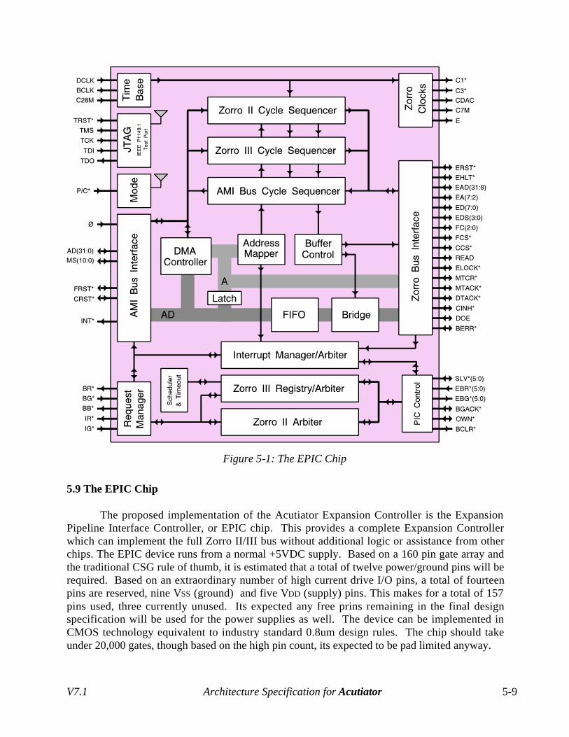
V7.1 Architecture Specification for Acutiator 5-9
5.9 The EPIC Chip
The proposed implementation of the Acutiator Expansion Controller is the Expansion Pipeline Interface Controller, or EPIC chip. This provides a complete Expansion Controller which can implement the full Zorro II/III bus without additional logic or assistance from other chips. The EPIC device runs from a normal +5VDC supply. Based on a 160 pin gate array and the traditional CSG rule of thumb, it is estimated that a total of twelve power/ground pins will be required. Based on an extraordinary number of high current drive I/O pins, a total of fourteen pins are reserved, nine VSS (ground) and five VDD (supply) pins. This makes for a total of 157 pins used, three currently unused. Its expected any free prins remaining in the final design specification will be used for the power supplies as well. The device can be implemented in CMOS technology equivalent to industry standard 0.8um design rules. The chip should take under 20,000 gates, though based on the high pin count, its expected to be pad limited anyway.
Figure 5-1: The EPIC Chip

Chapter 5: The Expansion Controller V7.15-10
5.10 Register Map
As with all Acutiator chips, the EPIC chip has a set of 32-bit registers at its own Controller-mode preassigned address, $00D8XXXX. These registers are designed for single, serialized, uncached access, accessable in supervisor data space only. A table of the twenty-one EPIC registers is show in Figure 5-2. These control various aspects of the EPIC FIFO, DMA controller, Zorro channels, and bus-to-bus tranfer functions. The EPIC chip is designed to support six Zorro expansion slots and an eight word FIFO, but the register map is designed to allow these items to be extended naturally. Some registers are active only in Controller mode, while others are applicable only to PIC mode.
In PIC-mode, the EPIC chip registers take up the first 4K of the PIC's memory, if enabled, once configuration is complete. Rather than respond to $00D8XXXX, the EPIC chip responds to the Zorro III configuration address for configuration, then its configuration-assigned address from then on. PIC registers, like Controller registers, are available independently from both sides of the bus. If the PIC registers aren't useful, they can be disabled via the PIC's controller configuration register. When disabled. chip selects and normal autoconfig support are available, but the DMA controller, interrupt handler, etc. are unavailable. Following are descriptions of the individual registers.
Figure 5-2: EPIC Register Map
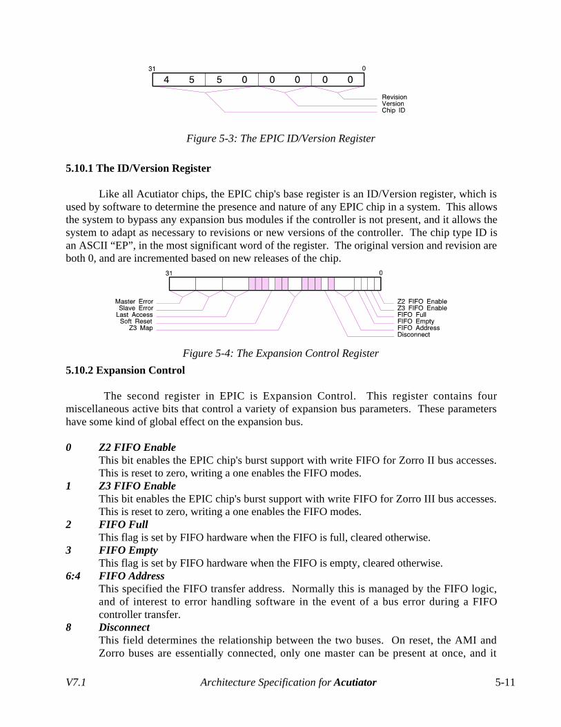
V7.1 Architecture Specification for Acutiator 5-11
5.10.1 The ID/Version Register
Like all Acutiator chips, the EPIC chip's base register is an ID/Version register, which is used by software to determine the presence and nature of any EPIC chip in a system. This allows the system to bypass any expansion bus modules if the controller is not present, and it allows the system to adapt as necessary to revisions or new versions of the controller. The chip type ID is an ASCII “EP”, in the most significant word of the register. The original version and revision are both 0, and are incremented based on new releases of the chip.
5.10.2 Expansion Control
The second register in EPIC is Expansion Control. This register contains four miscellaneous active bits that control a variety of expansion bus parameters. These parameters have some kind of global effect on the expansion bus.
0 Z2 FIFO EnableThis bit enables the EPIC chip's burst support with write FIFO for Zorro II bus accesses. This is reset to zero, writing a one enables the FIFO modes.
1 Z3 FIFO EnableThis bit enables the EPIC chip's burst support with write FIFO for Zorro III bus accesses. This is reset to zero, writing a one enables the FIFO modes.
2 FIFO FullThis flag is set by FIFO hardware when the FIFO is full, cleared otherwise.
3 FIFO EmptyThis flag is set by FIFO hardware when the FIFO is empty, cleared otherwise.
6:4 FIFO AddressThis specified the FIFO transfer address. Normally this is managed by the FIFO logic, and of interest to error handling software in the event of a bus error during a FIFO controller transfer.
8 DisconnectThis field determines the relationship between the two buses. On reset, the AMI and Zorro buses are essentially connected, only one master can be present at once, and it
Figure 5-3: The EPIC ID/Version Register
Figure 5-4: The Expansion Control Register
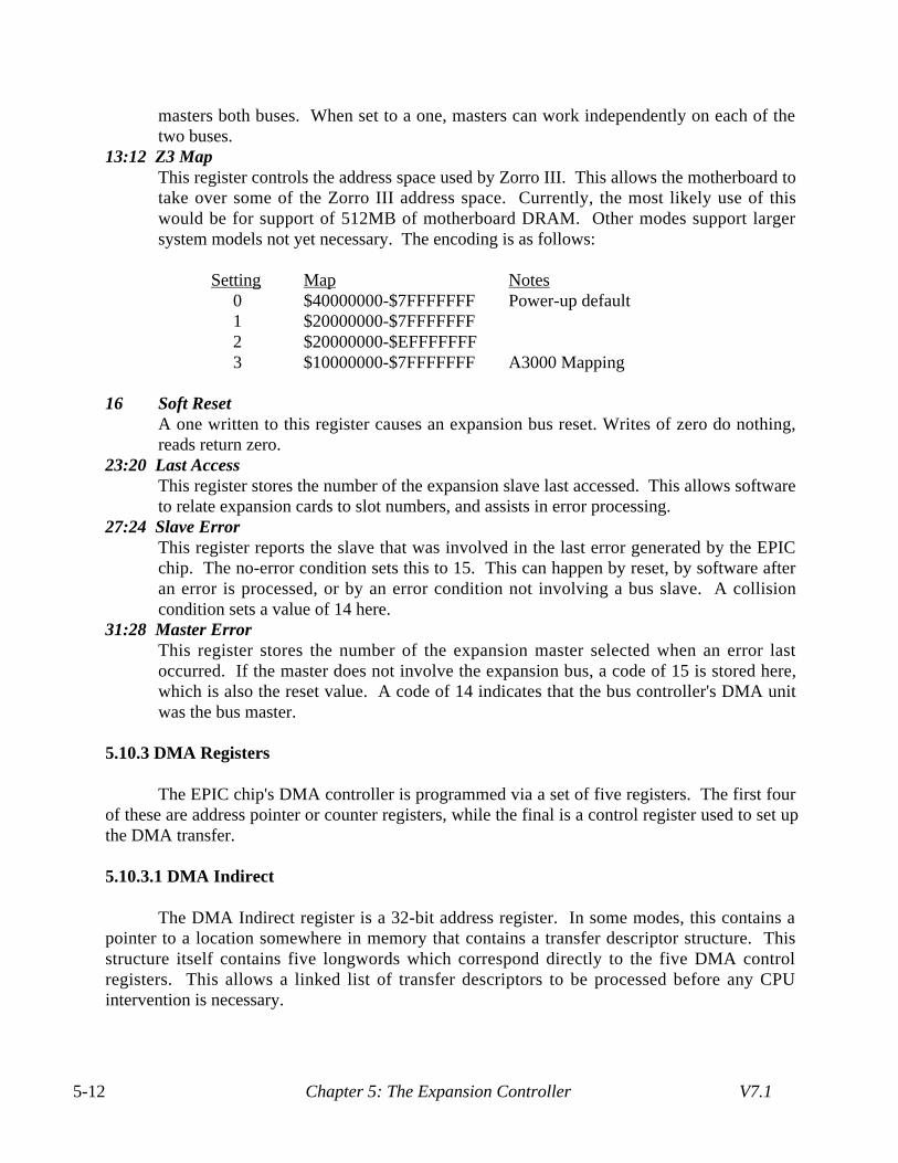
Chapter 5: The Expansion Controller V7.15-12
masters both buses. When set to a one, masters can work independently on each of the two buses.
13:12 Z3 MapThis register controls the address space used by Zorro III. This allows the motherboard to take over some of the Zorro III address space. Currently, the most likely use of this would be for support of 512MB of motherboard DRAM. Other modes support larger system models not yet necessary. The encoding is as follows:
Setting Map Notes 0 $40000000-$7FFFFFFF Power-up default 1 $20000000-$7FFFFFFF 2 $20000000-$EFFFFFFF 3 $10000000-$7FFFFFFF A3000 Mapping
16 Soft ResetA one written to this register causes an expansion bus reset. Writes of zero do nothing, reads return zero.
23:20 Last AccessThis register stores the number of the expansion slave last accessed. This allows software to relate expansion cards to slot numbers, and assists in error processing.
27:24 Slave ErrorThis register reports the slave that was involved in the last error generated by the EPIC chip. The no-error condition sets this to 15. This can happen by reset, by software after an error is processed, or by an error condition not involving a bus slave. A collision condition sets a value of 14 here.
31:28 Master ErrorThis register stores the number of the expansion master selected when an error last occurred. If the master does not involve the expansion bus, a code of 15 is stored here, which is also the reset value. A code of 14 indicates that the bus controller's DMA unit was the bus master.
5.10.3 DMA Registers
The EPIC chip's DMA controller is programmed via a set of five registers. The first four of these are address pointer or counter registers, while the final is a control register used to set up the DMA transfer.
5.10.3.1 DMA Indirect
The DMA Indirect register is a 32-bit address register. In some modes, this contains a pointer to a location somewhere in memory that contains a transfer descriptor structure. This structure itself contains five longwords which correspond directly to the five DMA control registers. This allows a linked list of transfer descriptors to be processed before any CPU intervention is necessary.

V7.1 Architecture Specification for Acutiator 5-13
5.10.3.2 DMA Source
This register contains a 32-bit source address for the DMA transfer. In most transfer modes, this register is incremented or decremented by one for each longword transferred. If source and destination are on different buses, cycles can be run on both buses simultaneously.
5.10.3.3 DMA Destination
This register contains a 32-bit destination address for the DMA transfer. In most transfer modes, this register is incremented or decremented by one for each longword transferred. If source and destination are on different buses, cycles can be run on both buses simultaneously.
5.10.3.4 DMA Count
This register contains a 32-bit count for the DMA transfer. This register is always decremented by one for each longword transferred during a DMA transfer. The EPIC chip can send an interrupt or run an indirect register load when this count passes zero.
5.10.3.5 DMA Control
The DMA Control register is responsible for determining the nature of the DMA transfer, and for actually starting the transfer when written. The bitfields are as follows:
1:0 Transfer ModeThe nature of the transfer is set by this register. When set to zero, no transfer takes place. When set to one, a simple longword by longword transfer takes place. When set to two, a burst by burst transfer takes place. Finally, when set to three, a bus optimized burst transfer takes place. This choice is the same as normal burst transfer when run on the same bus, but when run between the AMI bus and the Zorro bus, it causes the DMA controller to master the source bus, fill the FIFO, relinquish the source bus, master the destination bus, empty the FIFO, and then go back to the source bus again. This type of transfer can take longer than standard burst transfer, but it will use the system bandwidth more efficiently, so overall system performance may be boosted.
2 Transfer DirectionThis bit is set to 0 for an incrementing transfer, to a 1 for a decrementing transfer.
3 Source IncrementThis bit is set to cause source addresses to increment by one for each longword transferred. When clear, the source address does not increment.
Figure 5-5: The DMA Control Register
Chapter 5: The Expansion Controller V7.15-14
4 Destination IncrementThis bit is set to cause destination addresses to increment by one for each longword transferred. When clear, the destination address does not increment.
5 TC IndirectWhen the last longword of a DMA transfer is actually transferred, the terminal count condition is signalled in the DMA controller. Setting this bit causes a reload of the DMA registers from the DMA Indirect pointer following the terminal count.
6 Terminal CountThis bit is set by the DMA controller to indicate that the terminal count has been reached. This can be inspected to check if a transfer completed properly, though in general, if some other error wasn't register, the transfer did complete.
11:8 Interrupt PriorityThis sets the relative priority of the DMA controller interrupt with respect to the other expansion bus vectored interrupts.
13:12 Interrupt ModeThis specifies the interrupt behavior of the DMA transfer. When zero, no interrupt is generated. When set to one, a terminal count condition will cause an interrupt based on the interrupt priority and possible interrupt vector set. When set to two, the interrupt line is simply driven based on terminal count. A value of three is undefined.
14 Interrupt ReceivedThis bit is set by the DMA controller when an interrupt condition is signalled. Clearing this will clear a mode two interrupt or non-vectored mode one interrupt, while type one interrupts automatically clear in response to the interrupt vector cycle.
23:16 Interrupt VectorThis specifies an interrupt vector to use with mode one interrupts. When set to the reset state of zero, no vector cycle is run.
31:28 DMA PriorityThis register sets the priority of the DMA controller's activity relative to the channel priorities. The controller is treated as a Zorro III device for priority purposes (eg, it superceeds all Zorro II DMA).
5.10.4 Channel Control
The EPIC device supports one Channel Control register for each of its six expansion channels. These registers control various card-specific functions. There are a total of seventeen active bits in each register, broken up into five functional fields.
0 Z2 CacheThis bit, zeroed on reset, controls whether or not the particular card is cached for Zorro II memory access. A zero here inhibits caching, a one permits caching. All Zorro II I/O accesses are cache-inhibited.
1 Z2 LockThis bit determines the translation of locked AMI bus cycles to Zorro II cycles. Some Zorro II devices don't properly support the Zorro II locking mechanism. This resets to zero, which causes separate cycles to be generated. If set to one, EPIC generates appropriate TAS-lock read-modify-write cycles.

V7.1 Architecture Specification for Acutiator 5-15
2 Z2 UnsynchronizedThis bit determines the Zorro II DTACK* synchronization behavior. Technically, all Zorro II devices run a minimal four clock cycle, and a slave's DTACK* isn't sampled until the S4/S5 transition of the Zorro II cycle. While all bus masters have to support this, there's nothing technically preventing a slave from going faster. On reset, this bit is zeroed and all Zorro II access on the specific channel is normally synchronized. When set to one, slave-generated DTACK* is taken immediately, much like under Zorro III. This may permit some Zorro II cards to run faster without redesign. This is of course done at the risk of the user, unless the card is qualified by its manufacturer to handle this faster cycling.
4 Funnel To LongwordsWhen set, this bit causes words to be packed into longwords, or longwords to be broken down into words, for Zorro to AMI bus translations. If set for a Zorro III board, it causes D31-D16 to be used as the word, D15-D0 being ignored. This resets clear, permitting natural bus to bus conversions.
5 Funnel To BurstWhen set, this bit causes longwords to be packing up for burst cycles when going between the Zorro and AMI buses. When reset, bursts only take place when Zorro III devices request them.
6 Funnel UnincrementedWhen set, this bit causes the Zorro bus address to be held throughout a funneled transfer. This permits efficient I/O to AMI bus data funneling.
11:8 Interrupt PriorityThis field sets a priority for quick interrupts from the given channel. The reset value is zero, the priority is a four-bit signed value.
21:16 QuantumThis field specified the preferred optimal bus access quantum for the given channel as a Zorro III bus master. This resets to zero, which specified the default Zorro III arbiter quantum, generally eight cycles. The quantum is specified as a six-bit unsigned value.
31:28 PriorityThis field sets a priority for bus mastership from the given channel. The reset value is zero, the priority is a four-bit signed value.
5.10.5 AUTOCONFIGTM Control
This register is present only in PIC mode. It is initialized by various AUTOCONFIGTM registers when the host processor configures the board. Basically, when in PIC mode but unconfigured, the EPIC chip watches bus activity and uses this to set itself up.
Figure 5-6: The Channel Control Register
Chapter 5: The Expansion Controller V7.15-16
2:0 PIC SizeThis register follows the Zorro size conventions. It's initialized by a read to register 00, bits 2:0, during configuration. The value is used for determining how many bits out of the EPIC chip's configuration comparator are significant. The encodings, based in part on the Size Extension register as well, are as follows:
Extension=0 Extension=1 PIC Size Board Size Board Size
000 8 megabytes 16 megabytes001 64 kilobytes 32 megabytes010 128 kilobytes 64 megabytes011 256 kilobytes 128 megabytes100 512 kilobytes 256 megabytes 101 1 megabyte 512 megabytes110 2 megabytes 1 gigabyte111 4 megabytes RESERVED
3 Size ExensionZorro III size extension bit, from register 08. bit 5. This determines whether the Zorro II or Zorro III sizing conventions are used for the PIC Size register, as shown.
4 Autoboot ROMThis bit is set by the autoboot field in register 00. If there's a boot ROM, the ROM* select is still generated once the board is configured, with sizes given in the ROM Size field. If there's no boot ROM enabled, the ROM* select is generated only during configuration.
5 Cache InhibitThis bit is set by the device/memory bit in register 08. If the PIC is primarily of an I/O device nature, caching will automatically be inhibited after configuration
25:24 CS ModeThis field, from register 0C, sets the chip select controls for the PIC. When set to zero, no chip selects are generated. When set to one, CS4* covers the whole board. When set to two, CS4* covers the top half of the board, CS3*-CS0* are evenly spread over the bottom half. When set to three, CS4* covers the bottom three-fourths of the board, with CS3*-CS0* spread evenly over the top fourth of the board. ROM* always overlays this setup over its defined range, when enabled.
27:26 ROM SizeThis field controls the ROM* chip select. ROM* is always generated before configuration to enable the AUTOCONFIGTM ROM. Once configured, the ROM size varies based on the register 0C setting:
Figure 5-7: AUTOCONFIGTM Control Register
V7.1 Architecture Specification for Acutiator 5-17
ROM Size Meaning0 16K ROM1 64K ROM2 128K ROM3 512K ROM
28 HideThis bit sets the register hiding mode of the EPIC chip. When Hide is zero, the EPIC registers occupy the first 4K of PIC memory, overlaying any ROM or other chip select. When Hide is set, the registers go away after configuration.
29 Address DetectThis bit is used as a bus arbitration aid. When clear, a processor on the PIC bus must explicitly request the Zorro bus to force an arbitration and master the bus. When this bit is set, any address that falls off the PIC in the global system memory map causes an automatic bus arbitration.
5.10.6 Com Control
This register manages communications between the Zorro and PIC buses when in PIC mode. It manages interrupts between cards for simple I/O or multiprocessor signaling.
7:0 VectorThis register specifies an interrupt vector to be used by the PIC for Quick Interrupt cycles. It powers up zero, and if left zero, interrupt generation will be handled the Zorro II way.
10 TypeThis register specifies the type of interrupt input on the PIC side. It's set to the default of zero for a level-sensitive interrupt, set to one for an edge-sensitive interrupt.
11 PolarityThis bit powers up zero, indicating an active low/low-going interrupt expected at the input. A one written here causes an active high/high-going interrupt to be caught instead.
12 ReceivedThis bit reads one when EPIC registers a PIC-generated interrupt of the specified type and polarity. This can be written zero to clear.
13 Cause ZorroA one written here causes an interrupt on the Zorro bus, just as if the interrupt line were asserted in hardware. A PIC with processor on it may find this kind of interrupt simpler to generate than one using a hardware line.
Figure 5-8: Com Control Register

Chapter 5: The Expansion Controller V7.15-18
31 Cause PICA one written here causes an interrupt to the PIC bus. This bit will stay one until the interrupt is acknowledged.
5.10.7 Com Data
This is a simple dual-ported 32-bit register. Simultaneous read/write access is available between the AMI and Zorro sides of the chip. A bus lock on one side will hold off the completion of an access on the other side if they coincide. PICs can use this for simple communication with the AMI bus master without the need to provide shared memory.
511 Memory Mapping
The EPIC chip has very simple memory mapping rules. In PIC mode, the rules are all based on AUTOCONFIGTM: Configuration ROM responds at $FF000000 until configured, then the chip responds for the supplied board addresses. The individual chip selects within the board vary based on the board size, as mentioned previously. Both busses respond to the same address encoding, though the registers are dual ported and may be accessed simultaneously by both busses.
In Controller mode, the memory mapping is based on normal system mapping rules. The registers appear based at $00D80000 on the system or expansion bus. The Zorro II memory space is mapped from $00200000-$009FFFFF, while the Zorro II I/O space is mapped from $00A00000-$00B7FFFF, and from $00E80000-$00EFFFFF. Finally, the Zorro III space is mapped from $10000000-$7FFFFFFF.

V7.1 Architecture Specification for Acutiator 6-1
Chapter 6The CPU/RAM Controller
The CPU/RAM controller provides the interface between the host CPU, a large block of DRAM, and the AMI bus. This could be implemented using buffers, latches, and PALs, but an integrated solution is much more efficient. The DRAM controller benefits from the integrated solution, and total system performance benefits from a DRAM interface optimized for the host processor.
Any particular CPU is likely to have its own CPU/RAM controller chip. The point of this device is the creation of an optimized interface to the AMI and DRAM buses of an Acutiator motherboard. The part described here is for MC68040 and, optionally, MC68030/MC68030 processors. A CPU/RAM controller for any other CPU is likely to be similar, though actual details will vary some.
This chip manages the system ROM chip select as well, since ROM need to be on the CPU local bus to be cost effective and the DRAM controller's ROM mapping facility works hand in hand with the physical ROM select. Also managed here are four MC68040 bus DMA channels, which mix into a single AMI bus channel. This permits processor modules to easily support multiple bus masters, an advantage when the other bus masters directly support the MC68040 protocol. This also allows the same CPU/RAM controller to function on an alternate AMI bus module, perhaps to manage a CPU cluster in a multiprocessor system or another kind of '040 bus device that makes more sense as a separate AMI bus module. Other features exist as well, these will be covered in more detail in the specific sections of this chapter.
6.1 The JTAG Test Port
As in all Acutiator chips, a test port for the IEEE P1149.1 boundary scan protocol is defined. While such a port isn't vital to the operation of the device, we're convinced that board-wide JTAG support will be useful for both Chip and System testing. The pin requirements are:
Signal(s) CountClock 1Mode Select 1Data 2Reset 1
TOTAL 5
The actual test register map will be defined based on the chip implementation, it doesn't belong in this architecture specification. However, we do expect any implementation will at the least support the normal boundary scan functions.

Chapter 6: The CPU/RAM Controller6-2
6.2 The MC68040 Bus
The CPU/RAM controller is directly connected to the MC68040 address, data, and control bus. This is necessary to provide the highest performance CPU to DRAM interface possible. It also allows the CPU/RAM controller to provide an AMI bus interface for the MC68040 in a relatively efficient way. Along with the basic MC68040 bus, the CPU/RAM controller provides a bus arbiter and other CPU specific resources. The device allows the interface to be tuned specicially for different versions of the MC68040 and, optionally, the MC68020 or MC68030. This is set up in the configuration register, described in a later section.
In order to save on pin counts, only 8-bits of the MC68040 data bus is connected to the CPU/RAM controller. Controller registers are all 8-bit registers, though many form logical 32-bit groups. The pin count for the MC68040 bus interface is as follows:
Signal(s) CountCPU Clock 1Address Bus 32Data Bus 8Control Signals 16Interface Signals 1
TOTAL 58
MC68040 Bus Signals
CCLK The MC68040 Bus Clock.A31-A0 The MC68040 Address bus.D31-D24 The MC68040 Data bus.SIZ1-SIZ0 The MC68040 size control bits. These determine the size of the transfer
according to standard rules.TT1-TT0 The MC68040 transfer type bits. DRAM typically responds to standard
and MOVE16 types, registers only to standard Supervisor mode data cycles.
TM 1-TM 0 The MC68040 transfer modifier bits.R/W The MC68040 data transfer direction indicator.TS* The MC68040 transfer start strobe.TIP* The MC68040 transfer-in-progress strobe.MI* The MC68040 memory inhibit strobe. Memory and registers don't
respond to their assigned addresses when this strobe is asserted.LOCK* The MC68040 bus lock signal. This indicates an atomic operation is in
progress, the bus arbiter won't change masters as long as this is asserted.TCI* The MC68040 transfer cache inhibit signal. This is generated by a slave
device to inhibit the on-chip caches of the '040. In general, software support is also needed for cache control.
TBI* The MC68040 transfer burst inhibit signal. When a slave can't support a burst transfer, it generates this to tell the '040 not to burst.
V7.1 Architecture Specification for Acutiator 6-3
TA* The MC68040 transfer acknowledge signal. This is generated to cause a normal synchronous cycle transfer and termination.
TEA* MC68040 Transfer Error Acknowledge. The system records the AMI bus error code for processor examination.
IDIS* Disables interrupts to host MC68040.
A pair of bits in the configuration register set the processor type supported by the CPU/RAM controller. As mentioned, the support of the MC68030 and MC68020 are options that must be determined by the needs of the system design. While the MC68040 is the obvious choice for high-end systems in 1992, medium-range systems may still find the MC68030 or MC68020 desirable to use, especially since the Acutiator machines are designed to be modular. For support of these processors, the MC68040 bus interface pinout is remapped as follows:
MC68040 MC68030/MC68020TIP* AS*TM2-TM0 FC2-FC0
LOCK* RMC*TCI* CIIN*TBI* CBACK*TS* CBREQ*TA* STERM* ('030), DSACK1* & DSACK0* ('020)TEA* BERR*
Since there's no need to bus size, a 68030 can be driven completely from STERM*, whereas a 68020 can be driven from both DSACK* lines. In all modes, the appropriate CPU bus interrupt acknowledge cycle is translated into an AMI bus interrupt acknowledge cycle.
6.3 The AMI Bus Interface
An AMI bus port on the CPU/RAM controller allows an efficient conversion to be run between the MC68040 and the AMI bus for any time the MC68040 masters the AMI bus. This also simplifies the case when an AMI bus master needs to access the RAM bus, since the DRAM controls can be derived directly from the AMI bus signals, only AMI bus address and data need to be driven onto the MC68040 bus for DRAM access. The AMI bus A/D signal group is generated via buffer control signals generated in the CPU/RAM controller. Four 16-bit bidirectional latching buffers are driven directly by the controller and the various bus clocks, no extra glue is needed for this interface. The pins needed for this are as follows:
Signal(s) CountAMI Bus Clocks 3Master/Slave 11Address Buffer Control 3Data Buffer Control 3
TOTAL 20

Chapter 6: The CPU/RAM Controller6-4
While it's true that support of full address and data for both the MC68040 and AMI buses would result in a more efficient interface, it's just not enough of a performance boost to justify the massive size of the package that would require.
AMI Bus Signals
BCLK The AMI bus transaction clock, probably synchronous to the MC68040 clock. It's possible, but not necessary, to support asynchronous clocking of the AMI and MC68040 bus -- this is implementation dependent. Additionally, the synchronization phase between BCLK and CCLK is set by a bit in the configuration register.
DCLK The AMI bus double-speed clock.Ø The AMI bus phase clock.A/D31-A/D0 The AMI bus Address/Data group.ABDIR Direction control for the address buffers between AMI and MC68040
buses.ABLT Latching control for the address buffers between the two buses.ABOE* Output enable for the address buffers between the two buses.DBDIR Direction control for the data buffers between the AMI and MC68040
buses.DBLT Latching control for the data buffers between the two buses.DBOE* Output enable for the data buffers between the two buses.
The AMI bus requires that all burst cycles be inhibitable. If the MC68040 bus, or any other bus interface, has any reason to not always support burst inhibition, the CPU/RAM controller will need to manage burst shorting as part of the AMI bus interface. This is simply a way to quickly cancel a burst cycle that's overrunning what the responding AMI bus slave can handle. When the AMI bus slave is no longer responding to a cycle, but the cycle continues, the controller needs to continuously assert the MC68040's TA* signal until the cycle is terminated. This may be necessary for MC68060 processors if not the MC68040 today.
6.4 The DRAM Controller
The CPU/RAM controller manages a high-speed DRAM subsystem for the Host bus. The actual support logic included handles a total of 64MB, 128MB, 256MB, or 512MB of DRAM, depending on the configuration. It is specified with Fast Page Mode 32-bit JEDEC SIMMs in mind, but will of course support individual memory chips organized in a similar way.
The DRAM bus can be configured as a one, two, or four-way interleaved 32-bit bus or a one or two-way interleaved 64-bit bus. It's expected that the Acutiator systems will adopt a standard RAM bus socket either 64-bits or 128-bits wide, though current CPUs are of course not so wide. This interleave provides fast (four clocks at 25MHz with 80ns DRAM, though practically any DRAM speed is supported) initial access and one-clock burst read and write for any MC68040 bus device (AMI bus access it typically somewhat slower).
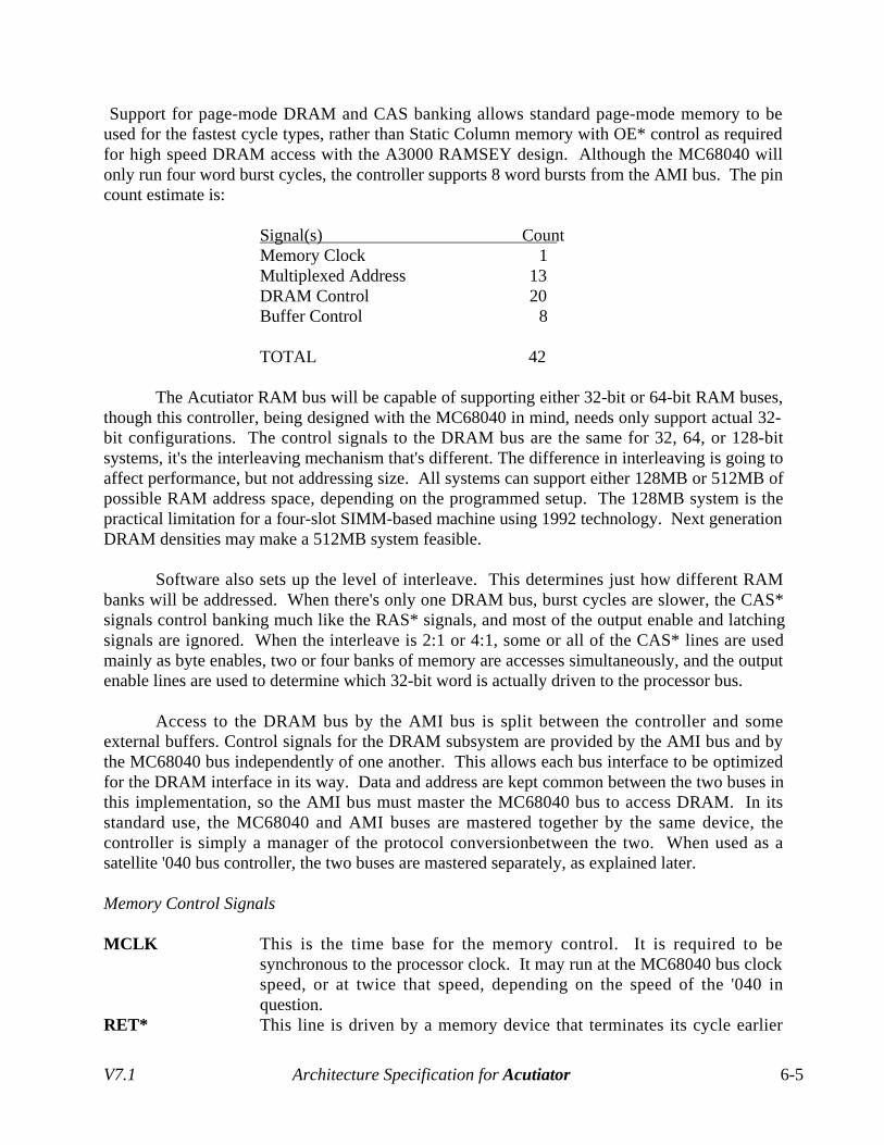
V7.1 Architecture Specification for Acutiator 6-5
Support for page-mode DRAM and CAS banking allows standard page-mode memory to be used for the fastest cycle types, rather than Static Column memory with OE* control as required for high speed DRAM access with the A3000 RAMSEY design. Although the MC68040 will only run four word burst cycles, the controller supports 8 word bursts from the AMI bus. The pin count estimate is:
Signal(s) CountMemory Clock 1Multiplexed Address 13DRAM Control 20Buffer Control 8
TOTAL 42
The Acutiator RAM bus will be capable of supporting either 32-bit or 64-bit RAM buses, though this controller, being designed with the MC68040 in mind, needs only support actual 32-bit configurations. The control signals to the DRAM bus are the same for 32, 64, or 128-bit systems, it's the interleaving mechanism that's different. The difference in interleaving is going to affect performance, but not addressing size. All systems can support either 128MB or 512MB of possible RAM address space, depending on the programmed setup. The 128MB system is the practical limitation for a four-slot SIMM-based machine using 1992 technology. Next generation DRAM densities may make a 512MB system feasible.
Software also sets up the level of interleave. This determines just how different RAM banks will be addressed. When there's only one DRAM bus, burst cycles are slower, the CAS* signals control banking much like the RAS* signals, and most of the output enable and latching signals are ignored. When the interleave is 2:1 or 4:1, some or all of the CAS* lines are used mainly as byte enables, two or four banks of memory are accesses simultaneously, and the output enable lines are used to determine which 32-bit word is actually driven to the processor bus.
Access to the DRAM bus by the AMI bus is split between the controller and some external buffers. Control signals for the DRAM subsystem are provided by the AMI bus and by the MC68040 bus independently of one another. This allows each bus interface to be optimized for the DRAM interface in its way. Data and address are kept common between the two buses in this implementation, so the AMI bus must master the MC68040 bus to access DRAM. In its standard use, the MC68040 and AMI buses are mastered together by the same device, the controller is simply a manager of the protocol conversionbetween the two. When used as a satellite '040 bus controller, the two buses are mastered separately, as explained later.
Memory Control Signals
MCLK This is the time base for the memory control. It is required to be synchronous to the processor clock. It may run at the MC68040 bus clock speed, or at twice that speed, depending on the speed of the '040 in question.
RET* This line is driven by a memory device that terminates its cycle earlier
Chapter 6: The CPU/RAM Controller6-6
than expected, as for memory devices with some kind of on-chip cache.MA 13-MA 0 Main multiplexed address bus. MA13 is only active for large mode
systems, when SIMMs exceed 32MBx32. These should be high current outputs, capable of driving all the DRAM that may be attached.
CAS15*-CAS0* Column address strobes. They manage four banks, where the bank number for CASN is given by (N div 4) and the byte number in that bank by (N mod 4).
RAS1*-RAS0* Row address strobes, used to manage banks.WE* The common write enable strobe for the whole RAM bus. This should be
a high current output.DOE3*-DOE0* Data buffer enables for up to four-way interleaving.DLT 3-DLT 0* Data buffer latch for up to four-way interleaving.
6.5 The Bus Arbiter
The CPU/RAM controller provides a simple MC68040 convention bus arbiter. This permits up to four MC68040 bus devices to run on a single AMI bus channel. The arbiter runs in two basic modes, based on the setting of a single configuration pin. The standard mode is set for an Acutiator host module. In this mode, the master of the MC68040 bus and the master of the AMI bus are always the same. Any request for mastership of the MC68040 bus is turned directly into a request for mastership of the AMI bus, and the AMI grant becomes the MC68040 grant. Address comparators on each bus watch the current master's activity to determine the direction of the data buffers between the two buses.
The alternate bus mastering mode is set by a bit in the configuration register. When in this mode, the CPU/RAM controller supports a satellite AMI bus module based on the MC68040 bus. This is mainly for support of shared-memory coprocessors, as it can glue any MC68040 bus device to an Acutiator AMI bus interface, completely with DRAM interface and intelligent arbitration. In this case, there can be are different masters on the AMI and MC68040 buses. The only time the two buses actually connect is when one bus needs to address resources from the other one. Address comparators monitor the MC68040 bus for the need to cross over to the AMI bus. When the MC68040 bus master needs AMI bus access, it will generate a standard AMI bus request and wait until a grant is received. When the AMI bus master needs access to the MC68040 bus, it generates a bus crossing request, via external address decoding logic, or it generates an AMI bus coprocessor override cycle (note that the configuration register also contains the slot ID for this). The DMA control register in the controller determines the rearbitration latency for each mastership condition, and which bus gets priority over the other in the event of a simultaneous mutual cross-access request. Finally, the control registers for the CPU/RAM controller are seen by the MC68040 bus only; they overlap with the host processor's CPU/RAM controller registers and can only be changed by the satellite processor. The signals needed are:
Signal(s) CountMC68040 Bus Arbitration 9AMI Bus Arbitration 4
TOTAL 13

V7.1 Architecture Specification for Acutiator 6-7
Bus Arbitration Signals
BR3*-BR0* MC68040 bus request strobes.BG3*-BG0* MC68040 bus grant strobes.BB* MC68040 bus busy strobe.ABR* AMI bus request strobe.ABG* AMI bus grant strobe.ABB* AMI bus busy strobe.ABC* Bus crossing request from the AMI bus. This is used only in satellite
mode, and is generated by some external decoding logic. When this line is asserted, the controller responds as the AMI bus slave, removes the grant from any MC68040 bus master, and gates the AMI bus over to the MC68040 bus as soon as it can. This crossing is governed by the ABC* line, and will remain as long as the ABC* line is asserted or the AMI bus loses the bus based on crossing priorities set in the controller registers.
6.6 Other Local Functions
Currently, there are a couple of additional functions defined for the MC68040 bus. The controller chip generates a that of ROM select, and supports associated ROM remapping in RAM. ROM cycles with Chip RAM overlay generate a MI* condition on the AMI bus so that no Chip RAM controller will respond.
The controller also generates the autovector signal for the MC68040. This was considered processor-specific enough to want to include it here, though there's no reason it couldn't have been generated elsewhere. The controller waits for a device to respond on the AMI bus before asserting an autovector condition, since an AMI bus device may be supplying its own interrupt vector. Unlike the A3000's vector support, this can be pretty fast since the AMI bus will indicate that a slave is responding very quickly, even if the response itself takes a long time to generate.
Finally, there are various bits of configuration information needed by the controller setup at boot time. There is a clock output and data input for a small serial ROM to set up this configuration data. Note that there's no hard limit on the size of this ROM, but all bits beyond those defined for any implementation must return zero.
Signal(s) CountROM Select 1Autovector 1Configuration Control 2
TOTAL 4

Chapter 6: The CPU/RAM Controller6-8
Miscellaneous Local Functions
ROM* ROM Chip Select.AVEC* Interrupt autovector.CFCNT Configuration serial clock.CFSP Configuration serial data port.
6.7 CPU/RAM Controller Summary
The CPU/RAM controller provides a high performance DRAM controller for the MC68040 bus that's compatible with the Acutiator RAM bus conventions. Additionally, it supports an MC68040 to AMI bus interface with full arbitration control. It can also be used to support MC68040 bus multiprocessors in an Acutiator system. A summary of the required pins is a follows:
Figure 6-1: RACE Chip Block Diagram

V7.1 Architecture Specification for Acutiator 6-9
Signal(s) CountJTAG Test Port 5MC68040 Bus Interface 58AMI Bus Interface 20The DRAM Controller 42The Bus Arbiter 13Other Local Functions 4
GRAND TOTAL 142
That's the CPU/RAM Controller specification. The next few sections cover a suggested implementation of this part, some register maps, and other assorted features of the device not already convered.
Figure 6-2: RACE Logical Register Map
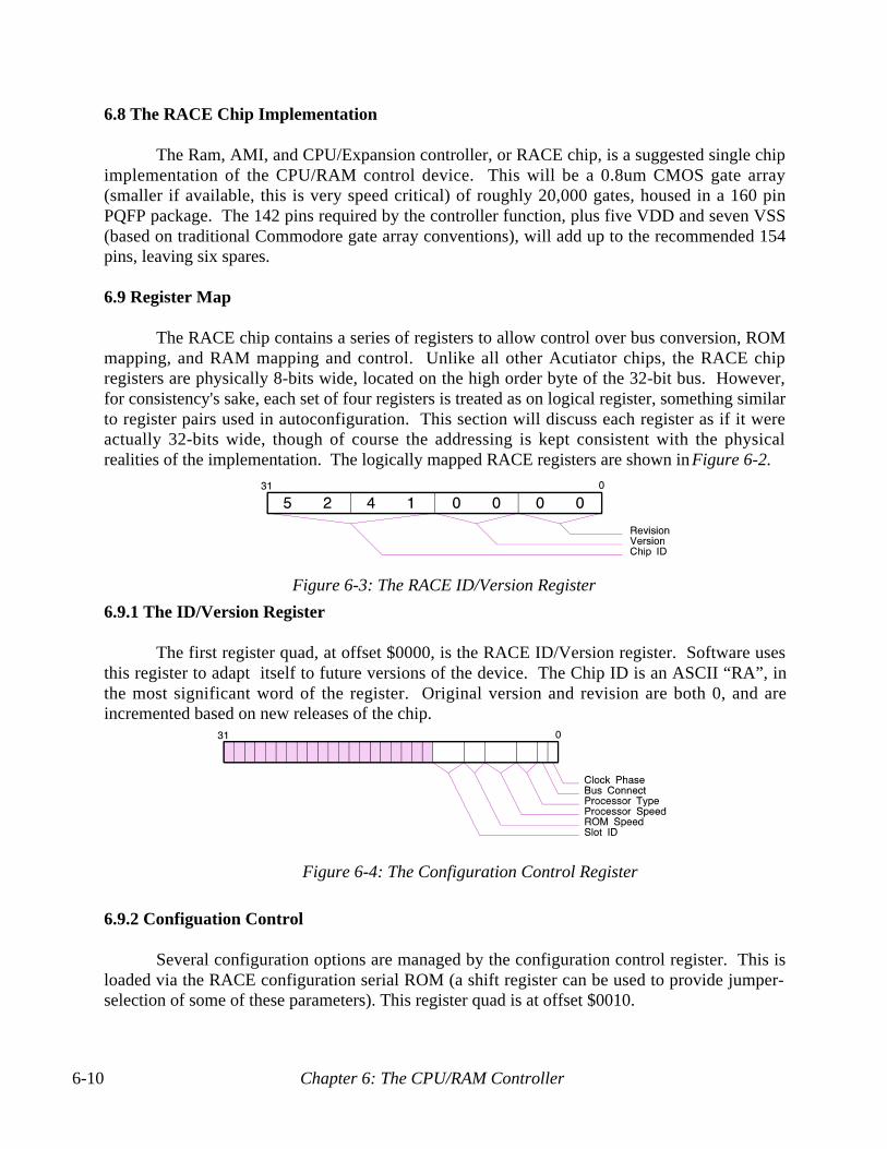
Chapter 6: The CPU/RAM Controller6-10
6.8 The RACE Chip Implementation
The Ram, AMI, and CPU/Expansion controller, or RACE chip, is a suggested single chip implementation of the CPU/RAM control device. This will be a 0.8um CMOS gate array (smaller if available, this is very speed critical) of roughly 20,000 gates, housed in a 160 pin PQFP package. The 142 pins required by the controller function, plus five VDD and seven VSS (based on traditional Commodore gate array conventions), will add up to the recommended 154 pins, leaving six spares.
6.9 Register Map
The RACE chip contains a series of registers to allow control over bus conversion, ROM mapping, and RAM mapping and control. Unlike all other Acutiator chips, the RACE chip registers are physically 8-bits wide, located on the high order byte of the 32-bit bus. However, for consistency's sake, each set of four registers is treated as on logical register, something similar to register pairs used in autoconfiguration. This section will discuss each register as if it were actually 32-bits wide, though of course the addressing is kept consistent with the physical realities of the implementation. The logically mapped RACE registers are shown in Figure 6-2.
6.9.1 The ID/Version Register
The first register quad, at offset $0000, is the RACE ID/Version register. Software uses this register to adapt itself to future versions of the device. The Chip ID is an ASCII “RA”, in the most significant word of the register. Original version and revision are both 0, and are incremented based on new releases of the chip.
6.9.2 Configuation Control
Several configuration options are managed by the configuration control register. This is loaded via the RACE configuration serial ROM (a shift register can be used to provide jumper-selection of some of these parameters). This register quad is at offset $0010.
Figure 6-3: The RACE ID/Version Register
Figure 6-4: The Configuration Control Register
V7.1 Architecture Specification for Acutiator 6-11
0 Clock PhaseThis bit sets the phase relationship between the AMI bus's BCLK and the MC68040 bus's CCLK. When zero, they're in phase, when one, they're 180° out of phase. This may help optimize theinterface, based on clock speed.
1 Bus ConnectThis bit determines the behavor of the MC68040 to AMI bus connections. If zero, the buses are connected together as usual, with all arbitration in common. This way, the current MC68040/AMI bus master has unblocked access to either bus, though of course only one master can be active at any given time. When set to one, each bus can run independently of each other, though they must run arbitrations when masters need the resources on each other's buses. The DMA Control register manages functions that relate to the use of this part as a satellite processor controller (eg, the two sides running independently).
3:2 Processor TypeThese bits determine the type of timing to generate for the processor specified:
Setting CPU Type0 Standard MC680401 Low-current MC68040 (MC68LC040, MC68EC040)
2 MC68030 3 MC68020
6:4 Procesor SpeedThis field indicates the speed of the MC68040 bus clock. The options are as follows:
Setting Speed 0 25 MHz 1 33 MHz 2 40 MHz 3 50 MHz 4-7 Reserved
8:7 ROM SpeedThis field specifies the speed of the system ROM. This lets the ROM speed be set on boot up without the ROM itself having to know how fast it is.
Setting Speed 0 100ns 1 150ns 2 200ns 3 300ns
11:9 Slot IDThis field contains the Acutiator system module slot number. The host processor is always slot zero, that's the only slot with a RAM bus extension on it.. When used as a satellite processor controller, the slot ID is read from the AMI bus connector and presented here. It's also used in the bus controller logic to detect a coprocessor override cycle directed at this device.

Chapter 6: The CPU/RAM Controller6-12
6.9.3 DMA Control
The next register quad, located at offset $0020, is the DMA control register. This is used to tune various aspects of the bus arbiter.
3:0 Select ChannelsWhile the RACE bus arbiter isn't as complex as the motherboard's arbitration scheme, it does have a little of that flavor. Following register fields allow the RACE chip to drive a Modifier code (TM2-TM0) and transfer type code (TT1-TT0) during DMA and, optionally, use a different bus request protocol. There are four bits here, one corresponding to each RACE DMA channel. If one is set, it uses the special protocol mode, if not, it uses the default MC68040 conventions.
6:4 Modifier TypeThis is the modifier code (TM2-TM0) that RACE will drive onto the MC68040 bus when a selected channel is the bus master. The transfer code in such a case is also driven to specify a normal transfer cycle.
7 Request ModeThis field, reset to zero on power-up, indicates the type of bus request generated by the potential master. If zero, the device supports the MC68040 style BR*/BG*/BB* protocol, including arbitration snoop. If one, the device supports a simple BR*/BG* protocol similar to that of the DSP3210.
19:16 68040 LatencyThis field determines how long the AMI bus should hold the MC68040 bus after a bus relinquish cycle.
23 Retry PriorityThis bit is set to determine which bus, in the event of a simultaneous cross access, should be retried. The default zero state causes the AMI bus to be retried, while setting this to one causes the MC68040 bus to be retried.
27:24 AMI LatencyThis field determines how long the MC68040 bus should hold the AMI bus after a bus relinquish cycle.
6.9.4 Coprocessor Communications
This register, located at $0030, is used to generate a coprocessor override cycle. The
Figure 6-6: The Coprocessor Communications Register
Figure 6-5: The DMA Control Register

V7.1 Architecture Specification for Acutiator 6-13
coprocessor number and command number are supplied during a write to this location, which is broadcast to the AMI bus. Either a coprocessor responds or the normal bus timeout ends the cycle with no coprocessor response.2:0 Coprocessor Number
This is the coprocessor number. During the initialization of a coprocessor module, this number is assigned by system software. All coprocessors detect a set to seven.
6:4 Coprocessor CommandThis is the three-bit coprocessor command code. The only command coprocessors so-far recognize is the bus relinquish command, code zero. This causes a coprocessor to get off its bus, useful when multiple coprocessors have local memory at the same global address and the host wants to master just one of them.
6.9.5 RAM/ROM Control
The next register manages basic overall physical structure of RAM and ROM. It also provides a facility for ROM-in-RAM mapping. This is located at $0100.
3:0 DRAM SizeThis register controls the basic size of a bank. One bank is the smallest independent RAS/CAS driven group, generally a whole or half of a SIMM module. The size, in K-longwords, is given by 2(DRAM Size + 8). The largest bank supportable is 64MB.
6:4 CAS BanksThis register indicates how many of the CAS-driven banks are present. There are always between one and four banks, the actual numbers possible depend on the bus interleave factor.
10:8 Bus InterleaveThis register specifies the number of buffered and latched banks of DRAM. This device can support one, two, or four banks.
13:12 ROM SizeThe ROM can be mapped for various sizes. This applies to both the physical ROM and any RAM emulation of it. The size are:
Setting Actual Size 0 512 K 1 1 MB 2 2 MB 3 4 MB
Figure 6-7: The RAM/ROM Control Register

Chapter 6: The CPU/RAM Controller6-14
14 ROM OverlayThis bit sets overlay of the low memory area on the system. Generally, this will be Chip RAM. The Chip RAM controller is kept from responding to this address by assertion of the MI* control when Chip overlay is done.
27:18 Overlay AddressThis field specifies the ROM base substitution address to generate when RAM is overlayingROM. This may apply to Chip RAM overlay or last through reset, depending on the setting of the Overlay Mode field.
31:30 Overlay ModeThis field determines just what the ROM in RAM translation function does, how long it lives, etc.
Setting Function 0 No overlay. 1 Overlay main ROM but not Chip RAM area, reset to zero. 2 Overaay all ROM areas, don't reset. 3 Reserved
6.9.6 RAM Base
This is a simple address register that locates the base address of the DRAM subsystem. The only real constraint is that it not conflict directly with another device and that it be an aligned address in Acutiator Fast RAM.
6.9.7 Refresh Control
The refresh control registers are based at $0020. There are four programmable 32-bit registers. The refresh cycle register determines the total number of clocks in a likely memory cycle. The refresh RAS and refresh CAS registers contain waveforms for RAS and CAS during refresh. Finally, the refresh count register determines the number of clocks that are counted between refresh cycles. All refresh is done with CAS-before-RAS protocols. With this programmable refresh generator, we should be able to support DRAM long into the future.
6.9.8 RAM Timing
There are four sets of six registers each devoted to the control of DRAM timing. The sets are at $0300 for single-beat reads, $0400 for single-beat writes, $0500 for burst reads, and $0600 for burst writes. Each RAM timing group consists of five waveform registers and a counter. The cycle counter determines the total number of clocks used for the DRAM cycle. The waveform registers drive RAS*, address MUX, CAS*, output-enable, and latch control based on this cycle count.
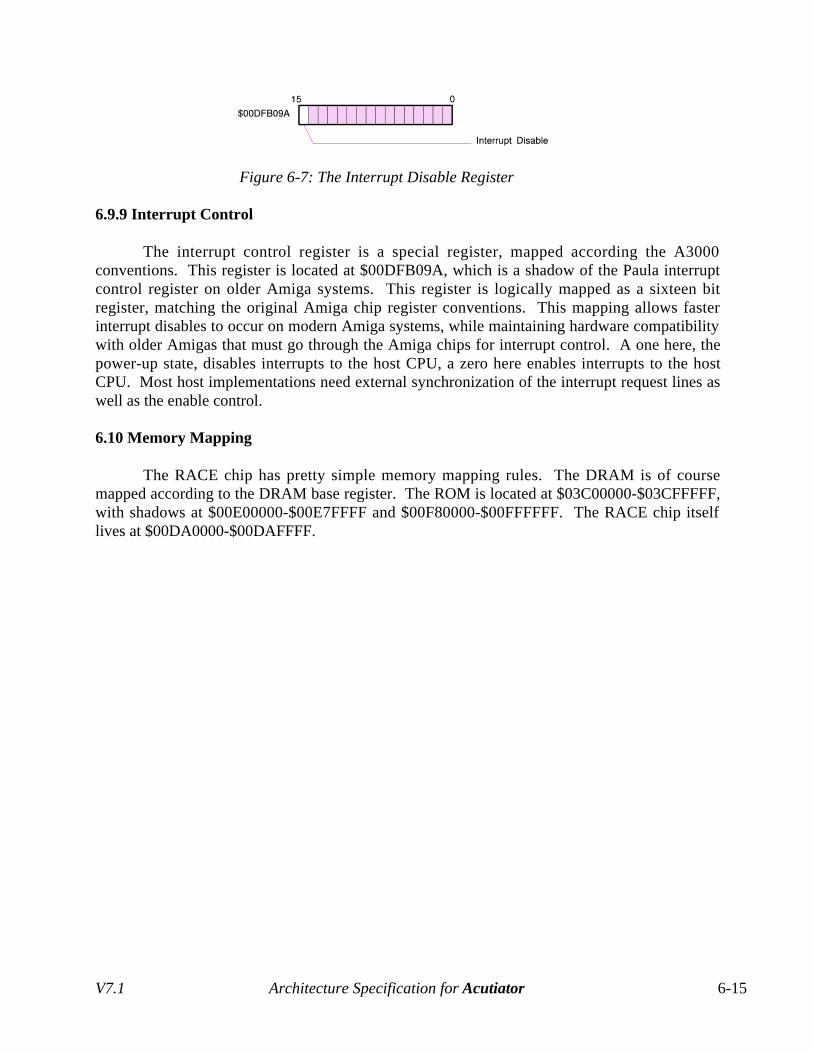
V7.1 Architecture Specification for Acutiator 6-15
6.9.9 Interrupt Control
The interrupt control register is a special register, mapped according the A3000 conventions. This register is located at $00DFB09A, which is a shadow of the Paula interrupt control register on older Amiga systems. This register is logically mapped as a sixteen bit register, matching the original Amiga chip register conventions. This mapping allows faster interrupt disables to occur on modern Amiga systems, while maintaining hardware compatibility with older Amigas that must go through the Amiga chips for interrupt control. A one here, the power-up state, disables interrupts to the host CPU, a zero here enables interrupts to the host CPU. Most host implementations need external synchronization of the interrupt request lines as well as the enable control.
6.10 Memory Mapping
The RACE chip has pretty simple memory mapping rules. The DRAM is of course mapped according to the DRAM base register. The ROM is located at $03C00000-$03CFFFFF, with shadows at $00E00000-$00E7FFFF and $00F80000-$00FFFFFF. The RACE chip itself lives at $00DA0000-$00DAFFFF.
Figure 6-7: The Interrupt Disable Register

Chapter 6: The CPU/RAM Controller6-16
V7.2 Architecture Specification for Acutiator 7-1
Chapter 7The AMI Bus
The Acutiator Modular Interconnect, or AMI bus, as briefly mentioned in preceeding chapters, is the bus interconnect used between Acutiator chips and modules. This bus is designed to address a number of important points:
• Compact bus size, important for system chip interconnects. Acutiator system gate arrays put a premium on pin count, so the AMI bus needs to keep pin counts down to a minimum.
• Easy processor interface. Ideally, a handful of low cost PAL and TTL devices should allow the basic 68030 or 68040 bus conversions.
• Processor neutrality. Without making the standard processor interface too complex, the bus needs to support a variety of possible processors without undue interface complexity, especially for low cost processors.
• High speed. The bus must maintain speeds necessary for nearly any motherboard. It must address interconnects with more speed and less cost overhead than an expansion bus at the loss of some generality.
The AMI bus is a multiplexed bus, based somewhat on Motorola family processor protocols. It is a fully synchronous bus, with a clock rate between 25MHz and 50MHz. There are two or three clocks, an Address/Data bus, and a Master/Slave control bus associated with the AMI bus. Two reset signals generally go along with the bus as well, but they are not a required part for all connections.
The main use of the AMI bus is for chip to chip interconnects. Secondary use is for intermodule interconnect, which in some cases amounts to the same thing. Toward this latter end, a connector is defined as a standard physical carrier for the AMI bus signals. The modular interconnect version of the AMI bus comes with some additional signals used for module configuration, I/O generation, and other useful functions. AMI bus cards are designed to be low-cost feature modules for a base Acutiator system, and this design is one way costs are kept down.
7.1 Component Signals
The AMI bus is a multiplexed 32-bit bus with support for 64-bit transfers. It is a synchronous bus based on a clock running between 25MHz and 50MHz†. The bus consists of three main signal groups. The clock group defines two or three clocks that control the other two groups. The A/D group defines a thirty-two wire address/data bus. Finally, the M/S group defines an eleven wire master/slave control bus.
†The clock rate is not a fixed value. We certainly need 25MHz-33MHz operation for any reasonably modern system performance. Looking forward, it would make sense to extend this to 40MHz-50MHz. Unlike previous designs, this will certainly require speed-graded parts for faster systems, possibly even using different gate array technologies.
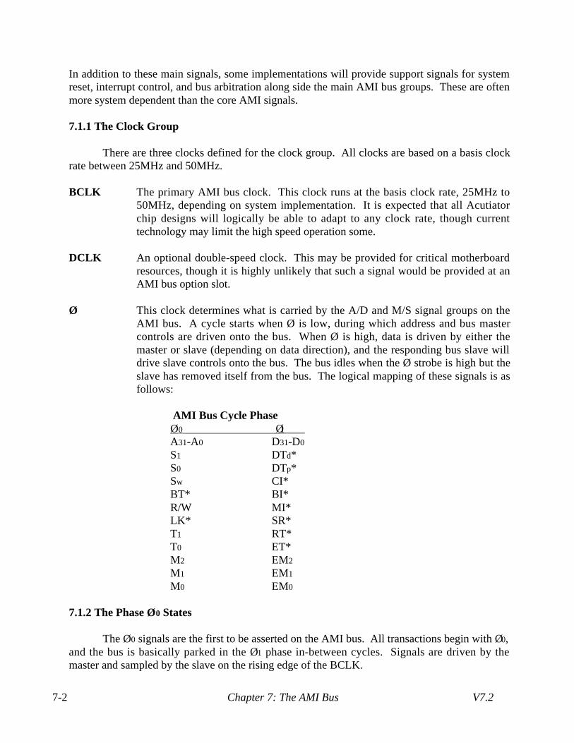
Chapter 7: The AMI Bus V7.27-2
In addition to these main signals, some implementations will provide support signals for system reset, interrupt control, and bus arbitration along side the main AMI bus groups. These are often more system dependent than the core AMI signals.
7.1.1 The Clock Group
There are three clocks defined for the clock group. All clocks are based on a basis clock rate between 25MHz and 50MHz.
BCLK The primary AMI bus clock. This clock runs at the basis clock rate, 25MHz to 50MHz, depending on system implementation. It is expected that all Acutiator chip designs will logically be able to adapt to any clock rate, though current technology may limit the high speed operation some.
DCLK An optional double-speed clock. This may be provided for critical motherboard resources, though it is highly unlikely that such a signal would be provided at an AMI bus option slot.
Ø This clock determines what is carried by the A/D and M/S signal groups on the AMI bus. A cycle starts when Ø is low, during which address and bus master controls are driven onto the bus. When Ø is high, data is driven by either the master or slave (depending on data direction), and the responding bus slave will drive slave controls onto the bus. The bus idles when the Ø strobe is high but the slave has removed itself from the bus. The logical mapping of these signals is as follows:
AMI Bus Cycle PhaseØ0 Ø1
A31-A0 D31-D0
S1 DTd*S0 DTp*Sw CI*BT* BI*R/W MI*LK* SR*T1 RT*T0 ET*M2 EM2
M1 EM1
M0 EM0
7.1.2 The Phase Ø0 States
The Ø0 signals are the first to be asserted on the AMI bus. All transactions begin with Ø0, and the bus is basically parked in the Ø1 phase in-between cycles. Signals are driven by the master and sampled by the slave on the rising edge of the BCLK.

V7.2 Architecture Specification for Acutiator 7-3
A31-A0 The 32-bit address bus.
S1, S0, SW The size of the transfer is indicated by these sizing strobes. All 64-bit transfers on the AMI bus are of course pseudo-64-bit transfers. Note that the burst enable strobe must be asserted to run a burst mode transfer.
S1 S0 SW Meaning 0 0 X Word (32-bits) 0 1 X Byte (8-bits) 1 0 X Half-Word (16-bits) 1 1 0 Word (32-bits, often burst) 1 1 1 Double-Word (64-bits)
BT* This strobe, burst transfer request, indicates the current master wants a burst cycle. If a master can't respond to slave burst inhibit, it must use an MMU to prevent burst cycles in areas that cannot support burst transfers. Bus slaves that can't support burst won't burst and will ignore cycles after their first. If a master can't inhibit bursting, it will need to monitor SR* and generate fake termination for the remaining burst transfers.
R/W This signal indicates the direction of a transfer across the AMI bus. If high, data flows from slave to master, if low, data flows from master to slave.
LK* This signal indicates that the current cycle is locked by the master. The bus arbiter will wait this line is negated during Ø0 before changing bus masters. This is designed for managing shared memory resources in a multiprocessor system, not as a way to hog the bus.
T1, T0 These are the cycle type indicator. They describe the type of cycle being run by the current bus master. Most slaves respond only to normal transfers, and uncachable bursts if they support burst transfers. They respond to special address spaces only if they contain hardware related to the special meaning of such spaces. The type encodings are:
T1 T0 Meaning 0 0 Normal transfer 0 1 Uncachable burst
1 0 Coprocessor override cycle 1 1 CPU special address space
M2-M0 These are the cycle type modifier codes. They further qualify the transfer indicated by the transfer type. Like the transfer modifiers, many of these may be CPU dependent. The AMI bus supports some standard meanings for normal transfers and uncachable burst transfers. Other meanings depend on the special function they indicate. Most slaves of a memory nature respond to User, MMU, Cache, and Supervisor accesses. Most slaves of an I/O, register, or control nature respond only to Supervisor Data accesses unless otherwise required (usually for

Chapter 7: The AMI Bus V7.27-4
compatibility), in which case they respond to User or Supervisor Data cycles. Coprocessor override cycles encode the coprocessor number on these lines. Basic encodings are:
M2 M1 M0 Meaning 0 0 0 Data cache push 0 0 1 User mode data access 0 1 0 User mode instruction access 0 1 1 MMU data table search 1 0 0 MMU instruction table search 1 0 1 Supervisor mode data access 1 1 0 Supervisor mode code access 1 1 1 Reserved
7.1.3 The Phase Ø1 States
The Ø1 signals are asserted on the AMI bus for the remainder of a bus cycle. The cycle may burst transfer four 32-bit words in 32-bit mode or eight 32-bit words in 64-bit mode. Bursts can be inhibited but not intrrupted, except when an error occurs. The signals are described below:
D31-D0 The 32-bit data bus. The state of the Ø0 R/W strobe determines whether master or slave drive this during the remainder of the cycle.
DTd* This is the double data termination strobe. During 64-bit mode transfers, this is asserted by the responding slave to indicate that a D64-D32 transfer is acknowledged. During bursts or pseudo-64-bit cycles, this word is transferred first. For other cycles, only one word is transferred and both acknowledges are asserted. True 64-bit systems use this strobe to latch the first word in either kind of pseudo-64-bit transfer.
DTp* This is the primary data termination strobe. This acknowledges all normal transfers. During 64-bit bursts or pseudo-64-bit transfers, this strobe indicates D31-D0 has been transferred. This mechanism allows DTp* to be the final transfer acknowledge indicator for all cycles.
CI* This is the cache inhibit strobe. This is asserted by a slave to inhibit caching of the transfer. Uncacheable transfers can only be bursts if an uncachable burst transfer is specifically called for. If a bus master can't respond to cache inhibit, it must make sure caching of uncachable resources is inhibited via MMU or other master-specific mechanism for all non-cacheable slaves.
BI* This is the burst inhibit strobe. This is asserted by a slave to inhibit bursting of the transfer. If a bus master cannot respond to the burst inhibit strobe, it must insure that bursting is inhibited via MMU or some other master-specific mechanism for all non-burstable slaves.
V7.2 Architecture Specification for Acutiator 7-5
MI* This is the memory inhibit strobe. This is actually monitored by all slaves. Its driven by a monitoring master, not the normal master or slave. Asserting this prevents the responding slave from actually responding. If it's negated before the end of the cycle, the slave then responds as normal.
RT* This is the retry termination strobe. A slave or pending bus master asserts this to cause the current cycle to terminate and retry. Usually, the system controller can generate this for a pending master, based on a bus access timout setting. All masters must do something reasonable when a retry is signalled. In conjunction with the bus arbiter this may generate a relinquish and retry cycle.
ET* This is the error termination strobe. It is asserted by a bus slave to indicate that some kind of problem with a transfer has occurred. This generally results in some kind of exception in the current master, and most of the time the host processor needs to intervene and properly process the error. The type of error is qualified by the EMN code.
EM2-EM0 These lines define the error modifier code. This code is asserted by a slave to indicate the type of error that has taken place. This will set the value of the error register in the Acutiator System controller chip, so that the host processor will have some idea about what kind of failure took place. For coproxessor override cycles, the override command is given on these lines. The error codes are:
EM2 EM1 EM0 Meaning 0 0 0 Module-generated AMI bus error0 0 1 Illegal access mode0 1 0 AMI bus timeout
0 1 1 Memory parity error1 0 0 Reserved1 0 1 PIC collision1 1 0 PIC-generated expansion bus error1 1 1 Unqualified AMI bus error
7.2 Bus Timing
The AMI bus timing is kept as simple and straight forward as possible. There are really just two sets of setup and hold times. The first set defines the time during which a signal can be driving the bus, with respect to the system clocks. The second set determines the time during which signals must be valid, with respect to the system clocks. The basic AMI bus cycle is shown in Figure 7-1.
AMI bus timing requirements vary by clock rate. While every system may not function at 50MHz, it is expected that most chips will support 50MHz clocks even if they don't function without wait-states there. The exceptions are for motherboard-based parts which are constrained to a speed-reated motherboard; these may be totally nonfunctional at higher clock rates. The following table illustrates the various parameters at the supported clock rates:

Chapter 7: The AMI Bus V7.27-6
No. Name 25MHz 33MHz 40MHz 50MHz 1 BCLK to signal on 0 ns 0 ns 0 ns 0 ns 2 Signal valid to BCLK 8 ns 6 ns 5 ns 4 ns 3 BCLK to signal invalid 8 ns 6 ns 5 ns 4 ns 4 Signal off to BCLK 0 ns 0 ns 0 ns 0 ns
7.3 Bus Transactions
The basic four-word transaction (32-bit burst) is shown in Figure 7-1. There are three other basic types of cycles: single-word, double-word (pseudo-64-bit), and eight-word (pseudo=64-bit burst). Each of these transaction types obeys the same basic timing shown for the four-word transaction. All bus slaves are required to handle single-word transactions, though it's highly desirable that they support all of the transaction types, at least where appropriate. Each of these types of cycles can take on wait-state variations, which allow both masters and slaves to insert extra cycles in order to guarantee proper operation at any clock speed.
7.3.1 Pseudo-64-bit Cycles
A detail of the pseudo-64-bit cycle is show in Figure 7-2. This is basically a double-length 32-bit transaction. Word transactions in pseudo-64-bit mode are actually two-word burst transaction, while bursts are actually eight-word 32-bit bursts. The main difference, other than the length, between 32-bit cycles and pseudo-64-bit cycles, is that both termination strobes are used during 64-bit transactions. This is designed to make it easy for a 64-bit bus master to easily handle the 32 to 64 bit funneling necessary for AMI bus access. In both 32-bit and 64-bit cycles, the DTp* strobe is the final cycle termination strobe. These cycle termination strobes are shown as separte signals in the following diagrams, but are of course actually part of the M/S signal group.
Figure 7-1: Basic AMI Bus Cycle
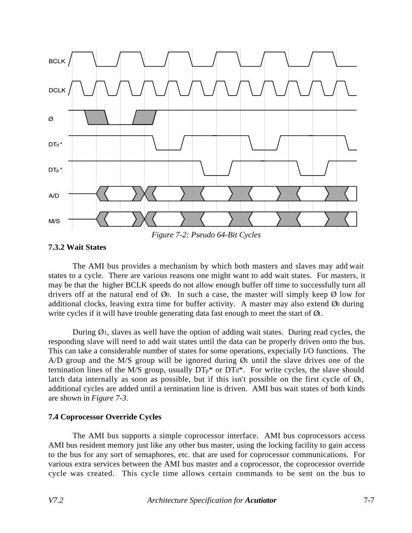
V7.2 Architecture Specification for Acutiator 7-7
7.3.2 Wait States
The AMI bus provides a mechanism by which both masters and slaves may add wait states to a cycle. There are various reasons one might want to add wait states. For masters, it may be that the higher BCLK speeds do not allow enough buffer off time to successfully turn all drivers off at the natural end of Ø0. In such a case, the master will simply keep Ø low for additional clocks, leaving extra time for buffer activity. A master may also extend Ø0 during write cycles if it will have trouble generating data fast enough to meet the start of Ø1.
During Ø1, slaves as well have the option of adding wait states. During read cycles, the responding slave will need to add wait states until the data can be properly driven onto the bus. This can take a considerable number of states for some operations, expecially I/O functions. The A/D group and the M/S group will be ignored during Ø1 until the slave drives one of the ternination lines of the M/S group, usually DTp* or DTd*. For write cycles, the slave should latch data internally as soon as possible, but if this isn't possible on the first cycle of Ø1, additional cycles are added until a ternination line is driven. AMI bus wait states of both kinds are shown in Figure 7-3.
7.4 Coprocessor Override Cycles
The AMI bus supports a simple coprocessor interface. AMI bus coprocessors access AMI bus resident memory just like any other bus master, using the locking facility to gain access to the bus for any sort of semaphores, etc. that are used for coprocessor communications. For various extra services between the AMI bus master and a coprocessor, the coprocessor override cycle was created. This cycle time allows certain commands to be sent on the bus to
Figure 7-2: Pseudo 64-Bit Cycles

Chapter 7: The AMI Bus V7.27-8
coprocessors as a normal AMI bus cycle. This cycle uses a special encoding of the T1-T0 lines, as described, along with the M2-M0 encoding the coprocessor number and the EM2-EM0 lines encoding the specific type of override function. Note that a general broadcast to all coprocessors can also be sent.
Coprocessor devices themselves can have private memory and other private resources not normally mapped into the AMI bus address space. The first coprocessor override function, level 0, causes the addressed coprocessor device to relinquish its private bus and allow the AMI bus master access to that bus. There must be some facility on the coprocessor device, of course, to allow the AMI bus access to the coprocessor's memory.
7.5 The AMI Bus Physical Connector
While the AMI bus is designed mainly as a simple and high-speed modular interconnect means, all modules in an Acutiator system are not necessarily located on the motherboard. Therefore, some means for adding various modules must be provided. The AMI bus slot definition is that means.
7.5.1 General Support Signals
To act as a practical and flexible modular interconnect, the AMI bus slot definition includes some signals not generally considered a required part of the AMI bus. These additional signals are as follows:
BFRST* This is the full-system reset. This signal is asserted onto the bus to indicate a full reset or power-up reset.
Figure 7-3: Wait States

V7.2 Architecture Specification for Acutiator 7-9
CRST* This is the CPU reset. This is asserted to reset the I/O system but not CPU-related elements of the system.
CNT The clock for the SSPB bus. SSPB is used on the AMI bus for simple configuration and other functions.
SP The data port for the SSPB bus.
SAD* The address strobe for the SSPB bus.
ID2-ID0 The slot ID code, used to allow a card to claim bussed slot-specific resources.
MP* This is the Module Present indicator. System logic may monitor this signal to determine if a module has been installed in any particular system slot.
7.5.2 Bus Arbitration Signals
Since the AMI bus is a multi-mastered bus, the AMI bus connector needs to support a handful of arbitration signals.
BR* This is a slot-specific bus grant. Actual grant lines are encoded by slot number and routed to their respective slots.
BG2-BG0 The bus grant generated by requests to the motherboard controller. The potential master compares its slot ID to the grant code to determine if it gets the grant.
BB* Bus busy strobe. This line is driven by a bus master or, depending on setup, the system controller, while some device is on the bus.
7.5.3 Coprocessor Support Signals
The AMI bus provides serialized I/O registers for simple coprocessor communitations. Additionally, it permits a coprocessor card to take over primary booting of the system from the Host processor.
CRC Coprocessor Register clock. This line clocks the serialized coprocessor register data.
CLD* Coprocessor Register load. This line loads data to or from a coprocessor control register.
CWR This is the slot-specific Coprocessor Write data line, which is converted by card hardware to an 8-bit output port.
CRD This its the slot-specific Coprocessor Read data line, which is converted by card

Chapter 7: The AMI Bus V7.27-10
hardware to an 8-bit input port.
CBOOT* This line is driven by a card to cause primary system booting to come from it, rather than from the Processor Slot Device.
7.5.4 Test Port Signals
Acutiator chips and many other modern chips support the JTAG boundary scan protocol (IEEE P1149.1), which permits detailed in-circuit test and troubleshooting. To allow modules to be part of the JTAG scan chain, these signals are brought out on the AMI bus.
TRST* JTAG (IEEE P1149.1) test port reset control.
TMS JTAG (IEEE P1149.1) test port mode select.
TCK JTAG (IEEE P1149.1) test port clock.
TDI JTAG (IEEE P1149.1) data input. For cards with no JTAG port, TDI is routed directly to TDO (empty slots achieve this via motherboard logic). Cards with a JTAG test port will describe their scan chain in the configuration ROM.
TDO JTAG (IEEE P1149.1) data output.
7.5.5 System I/O Signals
To aid in the support of low cost AMI bus I/O modules, the AMI bus will generarally be brought out with the System I/O bus available too. Extra memory and device selects are available for each slot, keyed to the slot ID code just as many other resources are. The system I/O group also supports a variety of interrupt signals, as follows:
C28M The I/O Bus Clock. Synchronous I/O transactions use this basis clock.
PA5-PA0 Peripheral addresses.
PD7-PD0 Peripheral data. There are a variety of 8 to 32 bit funneling options available for the actual transfers between this bus and the AMI bus.
E The 6502/6800 protocol clock.
R/W This is either a read/write strobe or a read enable strobe, depending on the selected mode of the device.
DS* This is either a data valid strobe or a write enable strobe, depending on the selected mode of the device.
PCS4-PCS0 These are the peripheral select codes. For AMI bus slots, an I/O select is available

V7.2 Architecture Specification for Acutiator 7-11
with PCS4 and PCS3 low, while a memory select is available with PCS4 low and PCS3 high, based on a slot ID match.
PDTACK* This is an asynchronous data acknowledge for self-timed peripherals.
PDL* This is the lower data word strobe for 16-bit transfers on the 8-bit bus.
7.5.6 The AMI Bus Slot Pinout
The following is a suggested pinout for the AMI bus physical connector. The recommended connector is a 112 pin, 50mil one piece edge connector. The signal arrangement is yet to be defined.

Chapter 7: The AMI Bus V7.27-12

V7.0 Architecture Specification for Acutiator 8-1
Chapter 8An Example System
This document proports to describe a system architecture, not a specific system. As an architecture, the Acutiator system can in theory describe any number of possible physical implementations. However, just as we described our views on chip implementations of the Acutiator architecture, this chapter discusses a system implementation.
8.1 The Highly Modular System Concept
The proposed basic Acutiator system design is what I'd term a Planned Highly Modular system architecture. The Highly Modular aspect is obvious; the motherboard system allows a great number of system details to be supplied on modular cards, rather than fixed into the motherboard design. A good portion of this capability comes from the way the Acutiator system is partitioned. The “planned” aspect is based on the idea, again, that the Acutiator system was designed from the ground up to exist as a series of modules. We'll include a short piece of history on modular systems that may help clarify this in a bit. That's an optional bit, you don't have to read it. We'd just like to make the point that, while modular systems seem to have become all the rage over the last few years, most of them are modular simply because a marketing department somewhere has decided that they should be modular. Amiga systems have been moving toward the goal of high modularity for some time now, for some very good reasons. The only thing that has held them back has been reluctance on the part of the product planners to go to highly modular systems. We hope this will change with realized Acutiator systems.
8.1.1 A Brief History of Modularity †
To some extent, the personal computer started out as a modular system. The orginal ur-PC was essentially a passive S-100 backplane into which the systems integrator would plug CPU, memory, and I/O boards in an effort to create a full fledged computer system. It was the “personalization” of the microcomputer in the mid-70s by Apple, Commodore, and Tandy that first gave you systems that were, to some degree or another, fixed function systems. Even at that, it was the expansion backplane in the Apple II, and its logical successor, the IBM PC, that brought forth truely successful and long lived computer systems. The expansion backplane in these machines was just another form of modularity. These backplanes eventually became suited only for low performance I/O, but they were, as much as anything, the reasons for the success of these systems. It has been a long term goal of the Amiga systems groups, both the originals in Los Gatos and the current in West Chester, to support and enhance this kind of capability in Amiga computers.
† As my observation, this section is obviously opionion, not hard fact. As someone who's been watching the microcomputer
industry just about as long as there has been a microcomputer industry, I hope it will be considered by the reader as an accurate observation.
Chapter 8: An Example System V7.08-2
There are a number of strong arguments for modularity. The need for an I/O backplane is an obvious one; no single base computer system can be all things to all people. Early systems required the I/O backplane to provide nearly all I/O; disk, ports, video, etc. Even while these items migrate to the system motherboard, higher performance version of the same become available for the I/O backplane, while new uses for this backplane are created every year. In the original Amiga 1000, the backplane was an add-on, and achieved limited success. When built into the Amiga 2000, a real platform system was created.
The Amiga 2000 actually took the modular concept one step further. It was obvious at the time of the A2000's design that the motherboard's 68000 would not be adequate for all the A2000's uses. Yet at the time, a 68020 processor was considered too expensive for the base A2000 system. The end result was the creation of the A2000 coprocessor slot, which made possible enhanced processors on relatively simple plug-in cards. The scope of the A2000 system didn't make this feature extremely elegant, but it made it very practical, and spawned a whole market in A2000 enhancement cards, as well as the A2500 machines bundled by Commodore itself. The A2500 development also made clear that such a modular design can drastically decrease the time to market of enhanced systems, especially when only one subsystem (CPU, Video, etc.) is being improved.
This concept was improved upon in the Amiga 3000. The coprocessor slot of the Amiga 3000 was designed with full forethough and consideration for the needs of an add on processor. Not only could an external CPU run it that slot, it could actively source the A3000 system clocks and efficiently share the A3000 local bus with the on-board 68030. It is also a trivial matter to eliminate the A3000's motherboard processors altogether and build A3000 class machines with the processor always on a plug in card, as ultimately done in the A3000T/040.
Modularity on Amiga systems reaches its logical conclusion at the Acutiator architecture. Acutiator, in as much as its possible without repartitioning the Amiga chip sets, makes every main component of an Amiga computer a modular element. It defines a standard interconnect for motherboard resources as well as expansion resources†. The Acutiator chips and both Local and System bus definitions make it much easier to connect a variety of processors with much less glue logic than required in previous Amiga systems. Traditionally motherboard related facilities can easily go on cards, and the number and type of such resources are very flexibly programmed, rather than being fixed in hardware as they were on previous systems. Finally, the motherboard itself is a module with respect to a finished system -- the same motherboard is used for all Acutiator configurations: pizza-box, small or large desktop, and tower systems alike.
8.1.2 Modularity and the Amiga
Modularity is not only a good idea, it's perhaps crucial to the success of anything but the cheapest low end Amiga system. Commodore is much smaller than a good portion of its competition, and willing to spend even less as a percentage of its size on new work than the
† This concept was first put forth here in a brief paper, “Toward the A4000”, by Dave Haynie, written up in 1990 shortly after the A3000 was finished. Needless to say, it has yet to be incorporated in an Amiga, though Sun and some in the PC Clone industry
are using the same basic concepts in their latest systems (eg, Sun's M-Bus, Intel's PCI, etc.).

V7.0 Architecture Specification for Acutiator 8-3
average computer company. Therefore, it depends much more on building platforms rather than one-use systems. And it shows; since the Amiga 1000 was introduced in 1985, Commodore has released only three fundamentally new high-end systems; Amiga 2000, 3000, and 4000. And these three system represent only two generations of system chips. Apple released more new systems than that in 1992 alone. Using the modular approach, however, the Amiga 2000 though 4000 became many different models.
However, neither system supports the creation of a highly modular motherboard, which is required to support both a broader range of Amiga computer products and the new Amiga technologies that are forthcoming. One Acutiator motherboard could support low profile systems with 68020, 68030, 68040, or 68060 processor modules, with or without multimedia (DSP) or high performance (FPU, DMA driven SCSI) options. Video option modules could cover ECS, “AA”, “AA+”, and both low and high end “AAA” subsystems. The same motherboard could be used for large desktop and/or tower machines. Even when one motherboard won't cover a whole line, modularization makes each new motherboard less work to design, build, and verify, and it can take advantage of the whole family of existing modules for CPU, video, expansion, etc.
This is good for Commodore, since any given addition to the matrix is an order of magnitude simpler and faster to implement than a whole new motherboard. It also makes it very easy to phase in cost reductions and improvements to one subsystem, since you replace only that subsystem, not the whole computer. A highly modular Amiga 3000† would have superceeded both today's Amiga 3000, the A3000T, and the A4000 and any possible “T” model to follow. The A4000 replacement “AA” implementations would have simply been a new video module.
This is good for the customer, since no one feels left behind when new technology is introduced. Even if separate upgrade modules ultimately cost as much as a complete new generation system, there's something psychologically comfortable to an upgrade of an existing system vs. a system replacement.
8.2 A Highly Modular Motherboard
A block diagram of an example highly modular Acutiator system is shown in Figure 8-1. The idea of a modular motherboard is that the main board itself strives to contain only those features that are useful for all systems or low cost enough to be redundant in some configurations. Technically, the motherboard could be a passive backplane, containing nothing but slots for I/O, processor, and memory. However, at a certain point, further modularization becomes counterproductive and expensive. Every system needs the ability to hook up to some fast memory and some basic I/O resources like keyboard, mouse, and floppy disk. While hard disk and networking at the very low end of Acutiator systems may not be critical, systems like IDE and RS-485, respectively, cost so little it's sensible not to omit these basics from the motherboard. Higher performance SCSI or Ethernet are available as add-ins, at least on the lower-cost systems. As always, what's modular in one implementation could easily become motherboard resident in a different implemetation.
† A modular video subsystem was originally proposed for the Amiga 3000, though we never considered a highly modular system at the time.

Chapter 8: An Example System V7.08-4
The key to the system's modularization are the available logical module slots. This suggested Acutiator defines four main kinds of module slots. These are not necessarily physically distinct in the actual system implementation, but they're logically defined, intended to be for the most part mixed as appropriate to the given motherboard. Module slots are somewhere between expansion slots and the old coprocessor slot in terms of reuseability. The expansion bus is expected to be supported, functionally unchanged, on any modular system. The coprocessor slot was a system-defined slot, subject to change for each new system implementation. Acutiator module slots are much more tightly coupled to system implementation than expansion slots, but at the very least designed to exist across multiple motherboards of the same generation if not across generations.
The primary module is the host processor module, which in nearly all cases will go in the system's single host slot. Normal modules have an AMI bus connector, while the host module adds the DRAM bus slot in-line with the AMI bus connector. The host module provides an AMI bus interface, a DRAM controller, and a system ROM. The card main contain other I/O or coprocessing devices; a processor module designed for Multimedia would contain a DSP3210
Figure 8-1: An Example Highly Modular System
V7.0 Architecture Specification for Acutiator 8-5
here. Typically, the interface logic for a CPU on this modules is minimal, especially if the RACE chip as defined in Chapter 6 is used.
For the addition of modules other than that of the host processor, the motherboard contains several AMI bus slots. Each of these slots provides the basic Acutiator Modular Interconnect Bus, the SSPB bus, and a DMA channel. A coprocessor interface channel is generally also provided, to help manage coprocesor devices like DSP or extra CPUs. Acutiator system chips are happy in such slots, and these serve as the basis for the rest of any complete Acutiator system. They can also be used for general purpose high speed expansion, including the addition of coprocessor devices and fast RAM. Most Finally, they may work in conjunction with the two other types of logical slots fo provide full featured I/O modularity.
There are two kinds of logical I/O slots. The first of these is the SysI/O slot. This is the basic support mechanism providing this Acutiator system with the capability to modularize things like expansion, port control, and video, while still allowing these things to work as they usually do in Amiga systems. So data channels for the motherboard supported RS-232 and floppy disk are available on this slot. Video data signals, both analog and digital, video clocks and other video related signals are on this connector, allowing a modular video card to drive a modular video expansion slot located on a totally different card. This is in some ways a “glue” slot. In the final design, it's possible that signals needed on the motherboard exist as a slot, while the rest of it takes the form of card-to-card cabling.
The final slot is the AuxI/O slot, designed for simple I/O expansion. This kind of slot contains the Acutiator peripheral bus management signals, some interrupts, and a both I/O and memory selects to be used by modules. Simple I/O ports, chip-selected peripherals, etc. can easily be located on modules this way. The SSPB serial ROM would be required to inform the OS of any modular device the system ROM doesn't already understand. This permits limited I/O devices to be added for very low cost, as if they were on the motherboard rather than in a general purpose expansion slot.
8.3 Some Processor Modules
There is a considerable bit of flexibility in the kind of host processor module that can be added to this example Acutiator system board. Figure 8-2 shows two possibilities. The first is essentially the lowest cost and lowest performance option, just a low-end processor and interface logic. The second is a multiprocessor host module, this one intended for high performance multimedia operations (several application optimized modules such as this could be offered).
On the low end of things is the basic processor module. Such modules contain only an MC680x0 type CPU and a small amount of processor-dependent logic to interface with the Acutiator Local Bus. Shown is an example MC68020 basic module. The host system ROM will be able to detect the MC680x0 processor type, so no system or SSPB ROM is necessary on this card. The system software configures all the programmable timing in the system based on the asynchronous 68020 bus (eg, it's essentially just advanced a state). A PAL is used to convert MC68020 control signals into their Acutiator bus equivalents in the few areas where they are not equivalents. As with all Acutiator host processor modules, this one supplies the two system bus
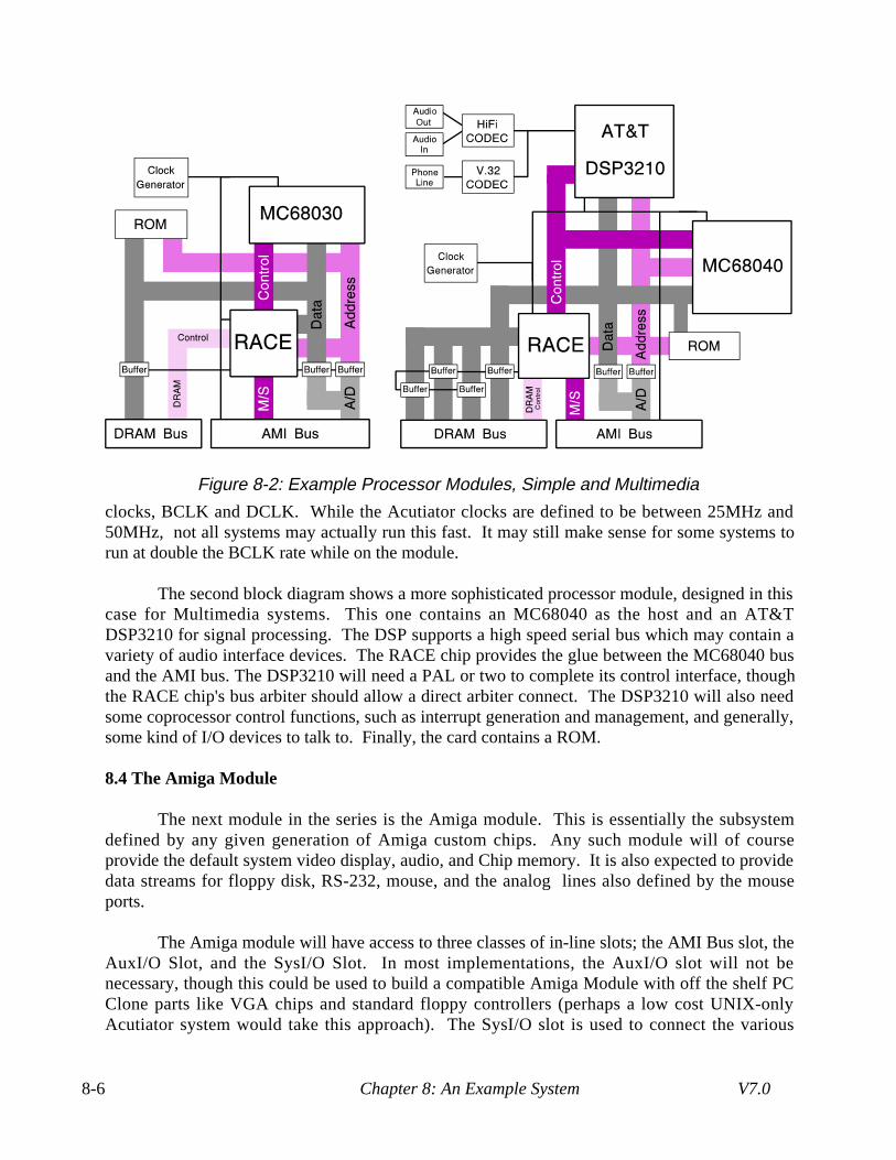
Chapter 8: An Example System V7.08-6
clocks, BCLK and DCLK. While the Acutiator clocks are defined to be between 25MHz and 50MHz, not all systems may actually run this fast. It may still make sense for some systems to run at double the BCLK rate while on the module.
The second block diagram shows a more sophisticated processor module, designed in this case for Multimedia systems. This one contains an MC68040 as the host and an AT&T DSP3210 for signal processing. The DSP supports a high speed serial bus which may contain a variety of audio interface devices. The RACE chip provides the glue between the MC68040 bus and the AMI bus. The DSP3210 will need a PAL or two to complete its control interface, though the RACE chip's bus arbiter should allow a direct arbiter connect. The DSP3210 will also need some coprocessor control functions, such as interrupt generation and management, and generally, some kind of I/O devices to talk to. Finally, the card contains a ROM.
8.4 The Amiga Module
The next module in the series is the Amiga module. This is essentially the subsystem defined by any given generation of Amiga custom chips. Any such module will of course provide the default system video display, audio, and Chip memory. It is also expected to provide data streams for floppy disk, RS-232, mouse, and the analog lines also defined by the mouse ports.
The Amiga module will have access to three classes of in-line slots; the AMI Bus slot, the AuxI/O Slot, and the SysI/O Slot. In most implementations, the AuxI/O slot will not be necessary, though this could be used to build a compatible Amiga Module with off the shelf PC Clone parts like VGA chips and standard floppy controllers (perhaps a low cost UNIX-only Acutiator system would take this approach). The SysI/O slot is used to connect the various
Figure 8-2: Example Processor Modules, Simple and Multimedia
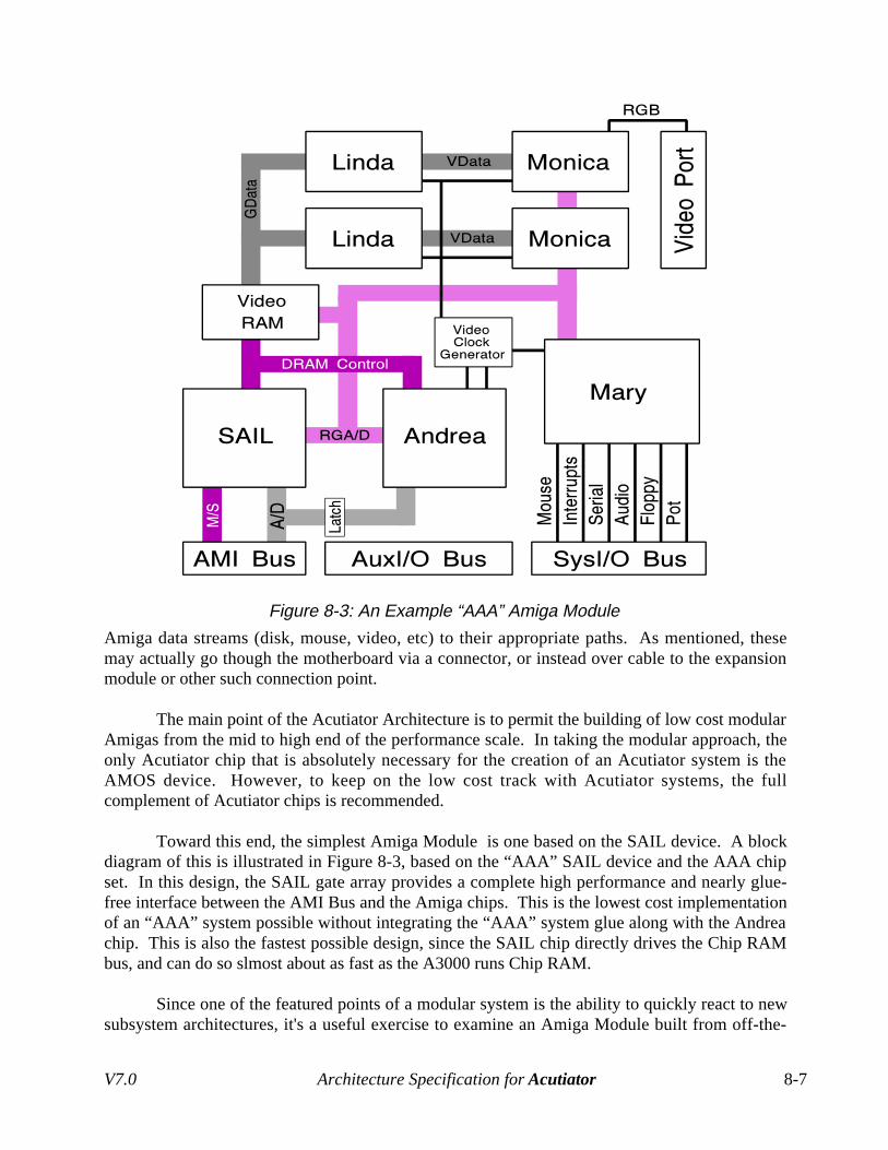
V7.0 Architecture Specification for Acutiator 8-7
Amiga data streams (disk, mouse, video, etc) to their appropriate paths. As mentioned, these may actually go though the motherboard via a connector, or instead over cable to the expansion module or other such connection point.
The main point of the Acutiator Architecture is to permit the building of low cost modular Amigas from the mid to high end of the performance scale. In taking the modular approach, the only Acutiator chip that is absolutely necessary for the creation of an Acutiator system is the AMOS device. However, to keep on the low cost track with Acutiator systems, the full complement of Acutiator chips is recommended.
Toward this end, the simplest Amiga Module is one based on the SAIL device. A block diagram of this is illustrated in Figure 8-3, based on the “AAA” SAIL device and the AAA chip set. In this design, the SAIL gate array provides a complete high performance and nearly glue-free interface between the AMI Bus and the Amiga chips. This is the lowest cost implementation of an “AAA” system possible without integrating the “AAA” system glue along with the Andrea chip. This is also the fastest possible design, since the SAIL chip directly drives the Chip RAM bus, and can do so slmost about as fast as the A3000 runs Chip RAM.
Since one of the featured points of a modular system is the ability to quickly react to new subsystem architectures, it's a useful exercise to examine an Amiga Module built from off-the-
Figure 8-3: An Example “AAA” Amiga Module

Chapter 8: An Example System V7.08-8
shelf parts. While it might be possible to build a new SAIL device with every new Amiga chip generation, it's not at all certain that such an effort will be necessary or even possible; resources may be better spent elsewhere, depending on the specifics of the situation. In other words, the modular architecture lends itself as much to the quick adaptation of new technologies as it does the creation of low cost systems. In fact, it makes the prototyping and development of new technologies much more efficient than what's done today, in that it's necessary only to prototype the new subsystem, not an entire new machine. So a prototype evaluation can be run over more units for less cost, and the prototype to production time is greatly lessened as a result.
We looked a little bit at a PAL and TTL implementation of an “AA” module for the Acutiator system. Such a module would be just a little more complex than the AA3000 or possibly A4000 version of an “AA” system. Typically, such a design would have somewhat lower performance than an integrated solution, and it would have a high cost. It's certainly possible to build a PAL/TTL module for system development and later phase in an integrated one. Even a production system could be managed this way.
8.5 The Expansion Module
The Expansion Module is shown in Figure 8-4. The design is very simple, since the EPIC chip takes care of all System Bus to Expansion Bus conversion in both directions, buffering, bus sizing for Zorro II support, etc. While this module is very simple, it's conceivable that with enough effort, an Expansion Module could be built based around the Fat Buster chip from the Amiga 3000. It would require at least ten TTL buffer chips for bus buffering and bridging, a bus mapping PAL, and some bus control conversion logic. While possible, it's not high efficient and not recommended.
The need for modular I/O expansion is not quite as obvious as the need for modularity in other subsystems. Certainly it's possible that you could put other expansion protocols into an Acutiator rather than the Amiga's Zorro bus. If the system were running the Apple Macintosh
Figure 8-4: The Expansion Module

V7.0 Architecture Specification for Acutiator 8-9
OS, certainly a NuBus backplane could be substituted. Similarly, with an EISA backplane and R4000 Host Module, you could turn the system into an Amiga-chip based ACE compatible computer. However, all of that amounts to a heck of a lot of work that's never likely to be done.
In much more practical terms, the Expansion Module has a reason for being. FIrst of all, in any low-profile Amiga, the expansion backplane is going to be on a daughtercard, to allow expansion cards to mount horizontally. It doesn't make much sense to create a new and different kind of motherboard socket for this backplane if the standardized modular solts will serve the same purpose. Making the expansion backplane modular in this manner also will allow a low-end version of the system to ship with expansion as an add-on option. While this could have been done on the Amiga 3000/A4000 class machines, most of the expansion costs were on the motherboard of that system in the first place. Finally, the Expansion Module makes sense if you think fo the whole Highly Modular Amiga Motherboard as a module itself. With the Expansion Module slots strategically located at the edge of the Motherboard, the same Motherboard can be used in a tower configuration. A right angle connector would be used instead of the normal vertical connector, with a mating daughterboard right next to the Motherboard taking cards in a normal tower system style configuration.
8.6 The Coprocessor Module
The final module type is for expansion only, few if any Acutiator systems would go out with such a module in them, at least not right away. A Coprocessor Module is a special case of the AMI bus module. In fact, it's not necessarily a special case at all. Coprocessor interface signals to aid the host/coprocessor communications exist on each open AMI bus slot. One slot has the CBOOT* signal, which permits it to grab the AMI bus before the host can.
This module has no single defined purpose; it can support multiple coprocessors, a high speed SCSI processor, extra memory, all kinds of things. In that it's much less general than the Zorro III bus, and in the suggested implementation, much smaller, we wouldn't recommed this slot be used for anything that could reasonably exist on an expansion card. Commodore-Amiga could, of course, claim this slot as their own for future unnamed expansion and force all third parties to use the general purpose expansion bus. In keeping with the Acutiator philosophy, this doesn't just permit very fast expansion, it also permits very cheap expansion, because the Motherboard Controller device is generating chip selects on the AuxI/O bus.
8.7 Physical Design Concepts
Until we get some physical design people involved, there can be no definitive statement about how a system like this would be mechanically configured. We do, however, have some ideas on the subject. To achieve a reasonable card size without building a giant motherboard (Acutiator Motherboards should be very small, as the example shown slightly smaller than full size in Figure 8-5), most implementations should be based on vertically mounted Module cards. However, we don't want to preclude the creation of low-profile systems like the A3000 or even two-slot machines like the A1000+ that was once proposed. Therefore, the Module cards should be small; probably no taller than 5-6cm high, 20cm long (obviously the Expansion Module will be larger, to accomodate Zorro bus slots). There's no requirement that the different types of
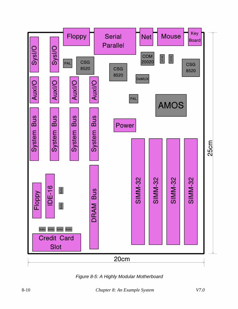
Chapter 8: An Example System V7.08-10
Figure 8-5: A Highly Modular Motherboard

V7.0 Architecture Specification for Acutiator 8-11
Modules all be the same size, but they will all fit within a specified maximum dimension to allow rational case designs.
The various bus connectors will be very high density connectors. The “KEL from Hell” style connector of the Amiga 3000 won't suffiice, because it doesn't permit vertically mounted cards. The high density IBM MicroChannel style edge connector is one candidate, since a one piece connector is generally cheaper and wastes less Module board space. However, such a connector precludes the building of “pizza box” style computers. It's very possible to build a single motherboard that would serve for pizza box, low profile desktop, and tower systems. In the pizza box systems, you don't use the Expansion or Coprocessor Modules, and you orient the Host and Amiga Modules horizontally. For the other systems, all modules are supported and are vertically oriented. Many of the high density two-piece connectors offer the plug-in board half of the connector in both straight and right angle versions; such a connector would facilitate this level of flexibility.

Chapter 8: An Example System V7.08-12