Architecture of an Advanced Synthesized Receiver for ...
93
Architecture of an Advanced Synthesized Receiver for Remote Control Applications by Aroosh R. Elahi A thesis submitted to The faculty of Graduate Studies and Research in partial fulfillment of the requirements for the degree of Masters of Applied Science in Electrical Engineering Ottawa-Carleton Institute for Electrical and Computer Engineering Department of Systems and Computer Engineering Carleton University Ottawa, Ontario, Canada June 12 th , 2008 ©Copyright 2008, Aroosh Elahi
Transcript of Architecture of an Advanced Synthesized Receiver for ...

Architecture of an Advanced Synthesized Receiver for
Remote Control Applications
by
Aroosh R. Elahi
A thesis submitted to
The faculty of Graduate Studies and Research
in partial fulfillment of
the requirements for the degree of
Masters of Applied Science in Electrical Engineering
Ottawa-Carleton Institute for Electrical and Computer Engineering
Department of Systems and Computer Engineering
Carleton University
Ottawa, Ontario, Canada
June 12th, 2008
©Copyright
2008, Aroosh Elahi

1*1 Library and Archives Canada
Published Heritage Branch
395 Wellington Street Ottawa ON K1A0N4 Canada
Bibliotheque et Archives Canada
Direction du Patrimoine de I'edition
395, rue Wellington Ottawa ON K1A0N4 Canada
Your file Votre reference ISBN: 978-0-494-44039-1 Our file Notre reference ISBN: 978-0-494-44039-1
NOTICE: The author has granted a nonexclusive license allowing Library and Archives Canada to reproduce, publish, archive, preserve, conserve, communicate to the public by telecommunication or on the Internet, loan, distribute and sell theses worldwide, for commercial or noncommercial purposes, in microform, paper, electronic and/or any other formats.
AVIS: L'auteur a accorde une licence non exclusive permettant a la Bibliotheque et Archives Canada de reproduire, publier, archiver, sauvegarder, conserver, transmettre au public par telecommunication ou par I'lnternet, prefer, distribuer et vendre des theses partout dans le monde, a des fins commerciales ou autres, sur support microforme, papier, electronique et/ou autres formats.
The author retains copyright ownership and moral rights in this thesis. Neither the thesis nor substantial extracts from it may be printed or otherwise reproduced without the author's permission.
L'auteur conserve la propriete du droit d'auteur et des droits moraux qui protege cette these. Ni la these ni des extraits substantiels de celle-ci ne doivent etre imprimes ou autrement reproduits sans son autorisation.
In compliance with the Canadian Privacy Act some supporting forms may have been removed from this thesis.
While these forms may be included in the document page count, their removal does not represent any loss of content from the thesis.
•*•
Canada
Conformement a la loi canadienne sur la protection de la vie privee, quelques formulaires secondaires ont ete enleves de cette these.
Bien que ces formulaires aient inclus dans la pagination, il n'y aura aucun contenu manquant.

Acknowledgments
It is a pleasure to thank the many people who made this thesis possible.
It is difficult to overstate my gratitude to my supervisor, Dr. Ioannis Lambadaris. With
his enthusiasm, his inspiration, and his great efforts to explain things clearly and simply,
he helped to make this research fun for me. Throughout my research, studies and thesis-
writing period, he provided encouragement, sound advice, good teaching, good company,
and lots of good ideas. I would have been lost without him.
I would also like to thank my friend Jorge Perez for his help on the PCB layout of the
receiver design; his assistance was instrumental in verifying the design parameters.
I wish to thank my entire extended family for providing a loving environment for me. My
brothers Sarmad and Omer, and my sister Sofia were particularly supportive.
Especially, I would like to give my special thanks to my wife Zaniab whose patient love
enabled me to complete this work and my daughter Ryka who really established the
deadline for completing this thesis!
Lastly, and most importantly, I wish to thank my parents, Rizwan Elahi and Arooj Elahi.
They bore me, raised me, supported me, taught me, and loved me. To them I dedicate this
thesis.
II

Abstract
This thesis presents a design of a narrow-band synthesized receiver system for remote
control applications. More and more critical infrastructure depends on wireless RF links
for command and control, hence reliability and robustness of the wireless link are of
paramount importance. While the transmitter is an integral part of any wireless link, we
focus on the receiver in this application because of its remote placement, size, power and
weight constraints and usually very harsh operating condition.
We present novel techniques for achieving good sensitivity and selectivity by means of
phase noise reduction in the local oscillator. We also describe other enhancements to the
back-end processing to achieve extremely reliable performance. All the concepts and
techniques described in this thesis were prototyped and tested on the bench and in the
field.
in

Contents
1 Introduction 1
2 Architecture of the Receiver 8
3 User Interface and Programmability 14
3.1.1 Frequency of operation 15
3.1.2 Failsafe modes 16
3.1.3 User defined per-channel failsafe programming 18
3.1.4 User defined channel-to-pin re-mapping 18
3.1.5 Enable different factory default and user defined pin mapping 19
3.1.6 Enable/Disable digital signal processing 19
3.1.7 Reset the receiver to factory default settings 20
4 Hardware Implementation 20
4.1 Power Supply Section 20
4.2 Micro-Controller Section 22
4.3 Antenna Section 26
4.4 LO Generation 28
4.4.1 VCO Section 28
4.4.2 PLL Section 30
4.4.2.1 Phase Lock Loop (PLL) 31
4.4.2.2 Phase Noise Reduction 33
4.4.2.3 Loop Filter Calculation 39
4.5 First Mixer 45
4.6 10.7 MHz IF Section 51
4.7 Limiter Section 51
4.8 Second Mixer (IF) 52
4.9 455 kHz IF Section 54
4.10 Discriminator Section/Baseband Recovery 55
4.11 Programmer Interface 55
5 Baseband Signal Processing 62
5.1 PPM Frame Protocol Basics 62
IV

5.2 Comparator Section 65
5.3 PPM Frame Search Procedure 66
5.4 Incoming Frame Filter 68
5.5 Frame Processing and Servo Output Calculation 69
5.6 Servo Outputs and Failsafe 70
6 Future Research Suggestions 71
6.1 Miniaturization 71
6.1.1 Digital Processing 71
6.1.2 Low-IF Architecture 72
6.1.3 CMOS Integration 72
6.2 Enhanced Reliability and Robustness 73
6.2.1 Front-end Filter 73
6.2.2 Spread Spectrum RF Link 73
6.2.3 Autonomous Operation 75
7 References 76
v

List of Figures
FIGURE 1: TYPICAL RC CHANNEL SPECTRUM 4 FIGURE 2: RECEIVER PROTOTYPE WITH TWO SERVOS CONNECTED 7 FIGURE 3: SELF-MIXING OF THE LO AND/OR OF AN INTERFERER IN A
HOMODYNE RECEIVER 9 FIGURE 4: SUPER-HETERODYNE MIXING 10 FIGURE 5: ARCHITECTURE OF THE SYNTHESIZED RECEIVER 13 FIGURE 6: PROGRAMMER HARDWARE 14 FIGURE 7: PROGRAMMER CONNECTED TO A RECEIVER 15 FIGURE 8: DUAL REGULATED POWER SUPPLY 22 FIGURE 9: MICRO-CONTROLLER BLOCK 24 FIGURE 10: ANTENNA CIRCUIT 26 FIGURE 11: ANTENNA CIRCUIT SIMULATION, S12 (LOG SCALE) 27 FIGURE 12: VCO CIRCUIT SCHEMATIC 29 FIGURE 13: PLL BLOCK DIAGRAM 31 FIGURE 14: ADF4001, BLOCK DIAGRAM 32 FIGURE 15: PLL SCHEMATIC 33 FIGURE 16: FLOWCHART FOR CALCULATING PLL PHASE-NOISE OPTIMIZED
N NUMBERS 37 FIGURE 17: HISTOGRAM OF THE N NUMBERS FOR THE RECEIVER 38 FIGURE 18: HISTOGRAM OF THE LO ERROR FOR THE RECEIVER 38 FIGURE 19: NOISE CONTRIBUTION OF ALL SOURCES EXCEPT VCO [41] 40 FIGURE 20: NOISE CONTRIBUTION OF THE VCO [41] 41 FIGURE 21: SETTLING TRANSIENTS 42 FIGURE 22: 2ND ORDER PASSIVE FILTER 43 FIGURE 23: DESIGN SPECIFICATIONS FOR THE 2ND ORDER LOOP FILTER... 44 FIGURE 24: MIXER BLOCK DIAGRAM 46 FIGURE 25: INTERMODULATION PRODUCTS 47 FIGURE 26: THIRD ORDER INTERCEPT POINT (IP3) 48 FIGURE 27: MOSFET MDCER SCHEMATIC 50 FIGURE 28: 10.7MHZ IF SECTION 51 FIGURE 29: LIMITER/AGC CIRCUITRY 52 FIGURE 30: SECOND STAGE MIXER, IF AND DEMODULATOR STAGE 53 FIGURE 31: CFUKG455KH1X-R0 FREQUENCY CHARACTERISTICS (NARROW
BAND) 54 FIGURE 32: CDBKB455KCAY07-R0 FREQUENCY CHARACTERISTICS 55 FIGURE 33: ROTARY BCD SWITCH CONNECTIONS 56 FIGURE 34: PROGRAMMER 57 FIGURE 35: PROGRAMMER SCHEMATIC 57
VI

FIGURE 36: PROGRAMMER RESISTOR CALCULATION FLOWCHART 60 FIGURE 37: POSITIVE AND NEGATIVE SHIFT PPM FRAMES 63 FIGURE 38: POSITIVE SHIFT PPM FRAME AND SERVO DECODING 64 FIGURE 39: BASEBAND CONDITIONING AND COMPARATOR OUTPUT 65 FIGURE 40: BOOT-UP SEQUENCE OF THE RECEIVER 67
VII

Table of Abbreviation
30IP
AC
A/D
ADC
AGC
BCD
CCP
DC
DSP
DSSS
ESC
FCC
FET
FHSS
FSK
ICP
ICSP
IF
INT
I/O
IP3
LC
LDO
Third Order Intermodulation Product
Alternating Current
Analog to Digital Converter
Analog to Digital Converter
Automatic Gain Control
Binary Coded Decimal
Capture Compare Port
Direct Current
Digital Signal Processor
Direct Sequence Spread Spectrum
Electronic Speed Control
Federal Communication Commission
Field Effect Transistor
Frequency Hopping Spread Spectrum
Frequency Shift Keying
In-Circuit Programming
In-Circuit Serial Programming
Intermediate Frequency
Interrupt
Input/Output Port
Third Order Intercept Point
Inductive/Capacitive
Low Dropout Regulator
viii

LED
LO
MCF
MCU
MOSFET
PFD
PLL
PPM
PWM
Q
RC
REF
RF
RSSI
SMD
SMT
SNR
TCXO
UAV
VCO
VLSI
XTAL
Light Emitting Diode
Local Oscillator
Monolithic Crystal Filter
Micro-Controller Unit
Metal Oxide Semiconductor Field Effect Transistor
Phase Frequency Detector
Phase Lock Loop
Pulse Position Modulation
Pulse Width Modulation
Quality Factor
Radio Control
Reference Frequency
Radio Frequency
Received Signal Strength Indication
Surface Mount Device
Surface Mount Technology
Signal to Noise Ratio
Temperature Compensated Crystal Oscillator
Unmanned Aerial Vehicle
Voltage Controlled Oscillator
Very large scale integration
Crystal Oscillator
IX

1 Introduction
Recent advances in semiconductor and wireless technologies have spawned numerous
new applications that were unfeasible or impossible to be realized just a few years ago
[30]. One such application that is attracting renewed global interest is the area of
remotely manned aerial and surface vehicles [45].
Unmanned vehicles are utilized in a very diverse set of applications, some utilizations of
unmanned vehicles that are remotely controlled are:
• Disaster monitoring: unmanned vehicles are used to monitor man made
and natural disasters, e.g. unmanned miniature helicopters were used
during the hurricane Katrina disaster in New Orleans [45].
• Airborne reconnaissance and combat: unmanned aerial vehicles
(UAVs) are used for reconnaissance and unmanned combat in Afghanistan
[31] [45].
• Infrastructure surveillance: unmanned vehicles are used for border
patrol and pipeline monitoring [26].
• Entertainment: airborne and surface unmanned miniature toy vehicles
are popular all over the world for personal enjoyment. A wide variety of
variations and types of miniature vehicles with sophisticated options exist
in the market [44].
• Education: miniature unmanned vehicles are an excellent form of
education tools to introduce not only advanced propulsion and
aerodynamic principles. They have also been successfully used to
demonstrate, motivate and improve learning abilities of students in areas
as diverse as electronic hardware design, integrated circuit design and
control systems [7] [28].
Most unmanned vehicles in operation have limited artificial intelligence and vision
processing capabilities and therefore require a remote human teleoperation control [1]
[30] [32] [45]. One of the most critical component of an unmanned system is the control
link between the vehicle and the human [26], in most cases the control link is wireless.
The wireless link infrastructure consists of a radio transmitter that modulates control
information in the form of data onto a carrier at the operator end. On the unmanned
vehicle a radio receiver removes the baseband from the carrier and processes the
demodulated data to forward it onwards to peripheral devices, e.g. servo motors,
propulsion control, camera, telemetry instruments, weapons, etc. The receiver has very
demanding performance requirements due to the following constraints:
• Weight: most unmanned vehicles have limited propulsion fuel, therefore
less weight translates into more endurance of the vehicle [30] [45].
• Size: real-estate is limited on most unmanned vehicles, and as such, a lot
of functionality has to be integrated in a small area [30] [32].
• Harsh operating environment: unmanned vehicles operate in harsh
environments where they're subjected to a wide variation in temperature,
intense G-forces, low frequency vibration in a very short span of time
[27]. Operation in the presence of strong in-band and out-of-band RF
2

signals is also a big concern. In hostile environments electronic warfare
and counter-measures against this threat is of paramount importance [30]
[31].
• Reliability: unmanned vehicles are sometimes used in very hostile
environment with operational time spans exceeding 24 hours [30].
The primary requirement for the performance of a receiver is its measure of sensitivity
and selectivity, sensitivity is measured in terms of the level of an RF signal that when
applied to the input of the receiver results in a specified signal to noise ratio at the output
of the receiver [22]. Selectivity is defined as the ability of the receiver to discriminate
between the intended signal in the presence of unwanted signal(s) [22].
The primary objective of this research is to develop architecture of an advanced RF
receiver system for remote control of unmanned vehicles. A complete end-to-end system
architecture and design is presented in the following sections. The receiver operates in the
72MHz and the 75MHz bands [43], the two bands are assigned for Remote Control
applications by the FCC (USA) and Industry Canada. The two bands are divided into
individual channels that are 20kHz wide with the output spectrum contained within
10kHz as depicted in Figure 1. The transmissions utilize binary Frequency Shift Keying
(FSK) whereby information is transmitted via two discrete variations of the carrier. The
modulation index defines the amount of FSK variation from the carrier and is around
2kHz for Radio Control applications. Following are some key features of this band for
RCuse:
72MHz: 50 channels, 20kHz apart, 72.01MHz-72.99MHz, 2kHz modulation
index either positive or negative.
3

75MHz: 20kHz apart, 75.41MHz-75.990MHz, 2kHz modulation index either
positive or negative.
f0-20kHz fO-lOkHz fO fO+lOkHz f0+20kHz
Figure 1: Typical RC channel spectrum
There are numerous commercially available receivers on the market that are targeted
towards the Remote Control applications. In comparison to the other areas of
conventional electronics the current state of commercial Radio Control receivers is quite
outdated. Most of the commercial receiver utilize designs that were conceived a couple of
decades ago. The following are some of the short-comings of the existing commercially
available receivers:
• All the existing receivers on the market are "non-crossover"; i.e. they
work either in the 72MHz band or the 75MHz band. This causes
additional efforts to manufacture and market receivers designed for the
two bands.
4

• Most of the commercial receivers work on just one kind of shift, either
negative or positive.
• Most of the receivers utilize sequential shift register based logic to
distribute the servo pulses to individual servos. This introduces excessive
jitter and glitches on the outputs.
• Most of the receivers utilize older technology and components that have
to be manually tuned and adjusted e.g. variable inductors and capacitors.
Vibration stress during operation routinely causes degraded performance
and severely reduces the life of the product.
• There are a couple of receivers on the market that offer synthesized LO
generation, however, the phase-noise of the LO signal is quite poor.
Furthermore, the design of these receivers is quite bulky and difficult to
utilize in smaller models, e.g. the Futaba synthesized receiver weighs
35.4grams and measures 53mmx33mmx20mm [49].
• None of the synthesized receivers offer easy field programming options.
• Most of the "High-end" receivers on the market cost upwards to U$150.
The receiver presented in this thesis presents the following enhancements:
• "Cross-over" operation. The receiver can operate on two bands and thus
cover all Radio Control applications.
5

• The receiver can operate on both the positive and the negative shift
transmitters available on the market. The operation is transparent to the
user and the shift determination is made automatically by the receiver.
• A micro-controller is utilized to process the baseband and de-multiplex the
PWM servo signals. Advanced algorithms to suppress glitches and to
discard corrupted frames are part of the baseband processing routines.
• Almost 95% of the components are surface mount, and none require
manual tuning and adjustment.
• The LO is synthesized and special techniques are utilized to reduce the
phase noise and bring performance as close to a monolithic crystal as
possible. The receiver is also very small and compact, it weighs only
7grams and measures 45mmx20mmx9mm.
• The receiver also features a modular programmer that is used to set
operational frequencies and can also be used to set different user defined
options. The programming can be achieved with relative ease in the field.
Some of the programming features are unique and are not present in any
previously available commercial product. The design of the programmer is
also quite unique, with a small passive resistor network and two BCD
encoded rotary switches 100 unique programming options can be realized
while only utilizing three pins of the micro-controller.
• The estimated commercial cost of the receiver is approximately U$65.
6

The receiver was prototyped in January 2007 and after minor adjustments to the
components and field trials that lasted 3 months, the product entered mass production.
The receiver is powered through a battery carried in the model, the outputs of the receiver
consist of a set of eight servo-pin connector. Servos and other peripherals e.g. camera
control, motor speed-controllers, etc. connected to this interface provide the control
mechanism for different functions. Figure 2 shows a picture of the prototyped receiver
with two servos connected.
Figure 2: Receiver prototype with two servos connected
7
2 Architecture of the Receiver
Rapid and widespread adoption of RF devices in the modern era translates into an
extremely busy RF environment, there are multitude users of the spectrum utilizing
different frequencies. This generates lots of interference and presence of strong and very
weak signals. The purpose of a receiver is to select the desired RF signal and demodulate
it to a baseband signal for further processing while rejecting all other signals that are of
no interest.
A good portable receiver architecture takes into account the complexity of the design,
power dissipation, size, number of components and performance [14]. A natural receiver
topology is a direct conversion, also known as a homodyne or zero-IF receiver
architecture that converts the RF directly to baseband [13]. The homodyne topology
offers simplicity, and is an attractive option for a compact and efficient design, however,
it has several shortcomings that impedes its widespread implementation and utilization
[14]:
• DC Offsets: Due to direct conversion to baseband, extraneous offset
voltages can corrupt the signal and saturate the following stages. The
offset voltages are created due to imperfect isolation between the local
oscillator (LO) port and the input RF port. Leakage of the LO to the RF
port are amplified and mixed with the LO signal in the mixer and thus
produce a DC component at the output, this phenomenon is called "self
mixing".
8

• Even-Order Distortion: Even-order distortions are problematic in
homodyne conversion, strong interferers close to the channel and LO
output duty cycle that deviates from 50% can produce even-order inter-
modulations that can corrupt the baseband signal.
• LO Leakage: The LO leakage can not only cause the phenomenon of
"self mixing", it can also be strong enough to cause interference to other
receivers as shown in Figure 3 [13]. This can be a real concern if a large
number of mobile receivers are operating in close proximity away from
their controlling transmitters which is a common occurrence during RC
competitions when a large number of models are operated simultaneously.
Interferer self-mixing
LO self-mixing
x
Figure 3: Self-mixing of the LO and/or of an interferer in a Homodyne Receiver
• Flicker Noise: In a homodyne receiver, the LNA and the mixer provide
limited gain to the downconverted signal thus making it quite sensitive to
9

noise. At low frequencies it becomes very important that baseband is
amplified with low noise.
IFlow IFhigh
Figure 4: Super-Heterodyne Mixing
The issues with the homodyne receivers as described above have prompted invention of
other architectures, the most notable being the super-heterodyne architecture [14]. Most
RF receivers offer very good sensitivity, this means that the receiver has to work with
very small signals and offers very large amplification on the order of 120dB or more [29].
The presence of a very weak signal (RF) and the amplification can cause coupling effects
and wreak havoc on the performance of the receiver, however, if the gain is spread over
several frequencies the effect of this coupling can be reduced, This is the fundamental
motivation for a super-heterodyne receiver [29]. In a super-heterodyne receiver the
incoming RF signal (Frf) is mixed with a local oscillator frequency (Fio) that is at an offset
from the RF frequency, the mixer output creates two components Ftf+Fio and Frf-Fio as
shown in Figure 4. The obvious goal is to shift the RF to a lower frequency signal, hence
10

the output of the mixer is bandpass filtered through an intermediate frequency filter that
only allows the Frf-Fio to pass to the next stage.
The super-heterodyne receiver solves all the homodyne receiver problems that were
mentioned above. The DC offsets of the front end are removed by bandpass IF filtering,
also, the LO leakage occurs at out of band frequencies and is suppressed by front-end
filtering and hence is no longer a big concern [14]. The most important feature of a super
heterodyne receiver is the superior selectivity that can be achieved even for a small
modulation index of a high frequency carrier [13]. Even with all its benefits the super
heterodyne receiver does present a number of drawback, the most significant being the
"image frequency", whereby the mixer translates frequencies above and below the local
oscillator frequency to the intermediate frequency as depicted in Figure 4. There are
numerous ways to solve this issue, each one presents its own pros and cons and the final
selection is dependent on the application [13] [14]:
• Choosing an IF frequency where the resultant image RF lies in an unused
part of the spectrum. This may not be a good solution as future utilization
of the spectrum can cause issues with the performance of the product.
• Choosing a very selective front-end filter, this can help in reducing the
level of undesired RF, however, it increases the number of components,
increases the filter loss and the Q requirements of the inductors may be
very difficult to achieve in a small SMT container. Also, even if high Q
filters are realizable they may require manual tuning which is prohibitive
for mass production of a commercial product.
11

• Choosing a high enough IF frequency so that the IF filter provides more
attenuation to the image frequency components. If a high IF is chosen to
attenuate image frequency components then it is important to chose an IF
filter that is no wider than the channel bandwidth and offers a high Q. In
some cases choosing a high IF may not be practical due to increased size
of the filter, cost and the design complexity.
• Use multiple conversion stage architecture. This technique can
significantly allow relaxation of the IF filter requirement by employing
multiple mixers and IF stages. Lower IF frequencies allow the utilization
of cheaper and more readily available IF filters that offer excellent
performance. However, this technique increases the component count and
complexity of the design.
The receiver architecture presented in this thesis is based upon the super-heterodyne
topology. There are two down conversion stages, with the first stage IF being 10.7MHz,
the second stage IF is 455kHz. The receiver employs a frontend band-select filter based
on discrete LC components that offers bandwidth of around 10MHz with the centre
frequency around 70MHz. The local oscillator is generated with a discrete VCO and a
varactor diode along with a low phase noise PLL. A micro-controller is employed to
control the PLL, process the baseband and provide control and programming interface to
the external peripherals and the user respectively. A system level block diagram of the
receiver is presented in Figure 5.
12

10.7MH
z IF filter
10.7MH
z IF
Lim
iter/AG
C
455kHz IF filter
455kHz IF r\
vco
PLL
11.355 MH
z C
rystal O
scillator
455 kHz
Ceram
ic
Discrim
inator
FIX
Programm
ing
Micro
-Co
ntro
ller U
nit
Baseband P
rocessor an
d PLL
Control
25MH
z
TGXO
T
J B
aseband Signal
Programm
er Interface Peripheral C
ontrol

3 User Interface and Programmability
The design offers a number of features that allow the user to customize the performance
of the receiver. The programming is achieved via the modular patent pending [20]
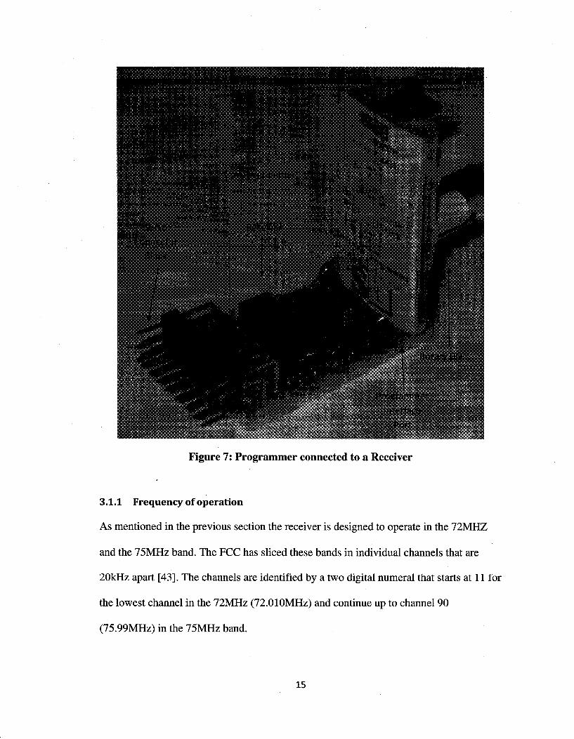
programmer hardware shown in Figure 6. Figure 7 shows the receiver with a
programmer connected. A full set of user defined features are described in detail in the
following sub-sections. Details on the design of the programmer are presented in section
4.11.
Figure 6: Programmer Hardware
14
Rotary Dials
Programmer
Interface
Port
Figure 7: Programmer connected to a Receiver
3.1.1 Frequency of operation
As mentioned in the previous section the receiver is designed to operate in the 72MHZ
and the 75MHz band. The FCC has sliced these bands in individual channels that are
20kHz apart [43]. The channels are identified by a two digital numeral that starts at 11 for
the lowest channel in the 72MHz (72.010MHz) and continue up to channel 90
(75.99MHz) in the 75MHz band.
15

To program a specific channel, the user determines the frequency of operation of the
transmitters and then dials this two digit number on the programmer by using the two
rotary switches. These two rotary switches are labeled 10's and 1 's to illustrate the most
significant and the least significant digit respectively.
Once the channel number is dialed-in, the user inserts the programmer in the respective
port on the receiver and pushes the push-button switch on the programmer. This action
immediately downloads the proper information to the receiver and it configures the
internal PLL to operate on this newly programmed channel.
The information remains stored on the non-volatile flash memory of the receiver, until
the user decides to re-program it or performs a factory reset.
3.1.2 Failsafe modes
In the event of the loss of transmitter-receiver link it is imperative that the model is
brought to a known state to avoid loss of property and/or injury. Different applications
require different failsafe strategies. The receiver offers the following three failsafe
options; the first two are factory programmed, while the third offers a complete user
control per individual channels:
a) Limited hold failsafe mode (default-factory pre-programmed): In this mode
the receiver will keep on driving the servos and other peripherals connected to its
servo-pin outputs with the last known good signal for lsec. After this interval, the
receiver will drive all servo-pin outputs low. This will cause all commercial ESC
(Electronic Speed Controllers) to shut-down the electric propulsion system after a
small timeout. The servo-pin outputs with servos connected will remain in the last
16

known good positions but will have no torque. In the event of a re-establishment
of the transmitter-receiver link, the receiver starts processing the received frame
and drives the servo-pins as in normal operation mode. This mode is already
programmed in the receiver and is selected to be the default factory failsafe mode
of operation. To explicitly select this mode the user dials in 98 on the
programmer.
b) Permanent hold failsafe mode (pre-programmed): In this mode the receiver
will keep on driving the servos and other peripherals connected to its servo-pin
outputs with the last known good signal indefinitely or until the transmitter-
receiver link is re-established. This mode is already programmed in the receiver,
however, to activate it, the user has to explicitly select this mode as a failsafe
operating mode. In the event of a re-establishment of the transmitter-receiver link,
the receiver starts processing the received frame and drives the servo-pins as in
normal operation mode. To explicitly select this mode the user dials in 97 on the
programmer.
c) User-defined per-channel failsafe mode: In this mode the user defines the servo
positions driven on the servo-pins when the transmitter-receiver link is severed.
Upon loss of link event, the receiver will keep on driving the servos and other
peripherals connected to its servo-pin outputs with the last known good signal for
lsec. after this short interval, each servo-pin will be driven by the respective user-
defined servo position value. In the event of a re-establishment of the transmitter-
receiver link, the receiver starts processing the received frame and drives the
17
servo-pins as in normal operation mode. The next section will detail the
programming aspect of this mode.
3.1.3 User defined per-channel failsafe programming
As defined in the previous section, the user selects the behavior of the individual servo-
pin channels in the event of the loss of transmitter-receiver link. To program this mode
the user selects the desired position of the servos connected to the receiver using the
transmitter. While holding these positions, the user (or a helper) dials 96 on the
programmer and pushes the push-button switch after inserting it on the receiver. This
causes the current servo positions to be captured by the receiver and stored in the internal
non-volatile flash memory.
3.1.4 User defined channel-to-pin re-mapping
In default factory mode, the servo-pins are assigned to logical channel in a progressive
manner, e.g. servo-pin 1 is assigned logical channel 1, servo-pin 2 is assigned logical
channel2, etc. However, in certain applications it is desirable to change this mapping to
accommodate logical channels that are higher than 8, or to drive two servos connected on
two different servo-pins with the same logical channel information. The receiver allows
for two channel-pin profiles to be stored on the non-volatile flash memory. The first user
defined map programming is initiated by dialing 91 on the programmer. The next step
requires defining the pin position followed by the logical channel number. The user can
choose to re-map one or all of the pins, once all pins are re-defmed, the programming
sequence is terminated by dialing 30 on the programmer.
18

3.1.5 Enable different factory default and user defined pin mapping
The receiver features two pre-programmed channel-pin mapping profiles, and two user
defined profiles as described in the previous section. The pre-programmed profiles are
called master and slave modes. In master mode, the pins are defined to output logical
channelsl-8 on servo-pinsl-8 respectively. The slave mode is used to extend the number
of logical channels that can be used in an application; by using two receivers, one
configured in master mode and the other in slave mode, the user can incorporate 16
servos in the application. In slave mode the receiver outputs channels9-16 on servo pinsl-
8 respectively. Master mode is selected by dialing 91 on tine, programmer, while the slave
mode selected by dialing 92 on the programmer.
The two user defined channel-pin mappings can be accessed by dialing 00 for user
setting 1 and 01 for user setting2 on the programmer.
3.1.6 Enable/Disable digital signal processing
The receiver allows the user to disable and enable the digital filtering employed to
remove glitches and check for the sanity of the frame before decoding it to generate servo
outputs. This is mainly used to diagnose noisy RF conditions in a controlled environment
or to allow the usage of a trainer setup, whereby two transmitters are connected together
to allow the trainer to grant or restrict control to a trainee to operate the model. Without
disabling digital signal processing the subtle differences in frame compositions of the two
transmitters will not allow the frames to pass through the rigorous checks implemented in
the firmware. The digital signal processing can be disabled by dialing 95 on the
programmer. The digital signal processing feature is enabled as a factory default,
however, it can explicitly be enabled by dialing 94 on the programmer.
19

3.1.7 Reset the receiver to factory default settings
Dialing 99 on the programmer erases all custom settings on the receiver and brings the
state of the receiver as per the factory defaults.
4 Hardware Implementation
The receiver is constructed on a 4-layer PCB, with a mix of SMT and through-hole
components. There are 55 unique components and a total of 109 components on the PCB.
The receiver measures 45.0mmx20.0mmx9.0mm and weighs approximately 7grams. The
following sub-sections describe in details the functionalities and design process for
different blocks of the receiver.
4.1 Power Supply Section
The power supply section of the receiver consists of a cascaded chain of two low drop
out (LDO) regulators. The receiver can operate with an input range of 3.8V - 9.0V. This
power supply configuration plays a fundamental role in the performance of the receiver
by providing additional suppression of power-supply transients.
There are various reasons for the generation of noise on the power-supply in the receiver:
• Servo noise: Servos are a common peripheral connected to the output of
the receiver. Servos translate and input PWM modulated electrical signal
into rotary mechanical motion. The servo arm is connected to different
control surfaces, e.g. wheels on a car, elevators of a plane, etc. Due to the
mechanical nature of servos they generate low frequency noise, they also
generate noise on the supply due to uneven current consumption e.g. when
20

a high load is presented to the servo arm or when the servo arm is
obstructed.
• Battery: An input supply battery with low charge or an input supply
battery with high internal resistance can cause momentary dips in the
output voltage of the battery when a high-current load is presented. These
dips can cause the first stage voltage regulator on the receiver to lose
regulation.
• Installation issues: Bad installation can also cause noise issues, e.g. long
and thin leads and leads with flaky electrical connections can offer a finite
resistance, for high currents, noisy voltages can occur in these wires and
cause the receiver to lose regulation.
The stability of the PLL+VCO is of utmost importance for a reliable RF link, the RF
performance of the receiver is directly linked to the phase-noise of the PLL [5] and the
phase noise of the PLL is related to the amount of noise on the power supply line,
Heydari et. al. present a very detailed analysis of the effect of power-supply noise on PLL
performance [4].
In the receiver, a 3.3V output and a 3.0V output regulators from National Semiconductor
Corporation are utilized. The LP2985 is a 150 mA low-noise ultra low-dropout regulator
in a SMD package that comes in a variety of output voltage configurations and offers
exceptional performance over a wide temperature range [34]. The output of the first stage
3.3V regulator is fed to a second stage regulator that drops down the input to a regulated
3.0V output as shown in Figure 8. The motivation of double regulation is to reduce and
21

smooth out the power-supply noise for the RF section. The performance of just a single
regulator is excellent, however, the utilization of two LP2985 cascaded together gives
additional noise suppression capabilities for relatively small increase in cost and PCB real
estate. The final 3.0V supply is ultra-stable and is used to power the RF section and the
two IF stages. The 3.3V supply is used only for the micro-controller section where
power-supply noise is non-critical.
3.8v-9.0V input from external
battery or power supply I..P2985IM5-3.3
3.3V regulated output from first stage regulator. This is the supply
for the micro-controller and art input to the second stage 3.0V
regulator
Ultra-stable 3.0V dual regulated output to
power the RF stages
Figure 8: Dual Regulated Power Supply
4.2 Micro-Controller Section
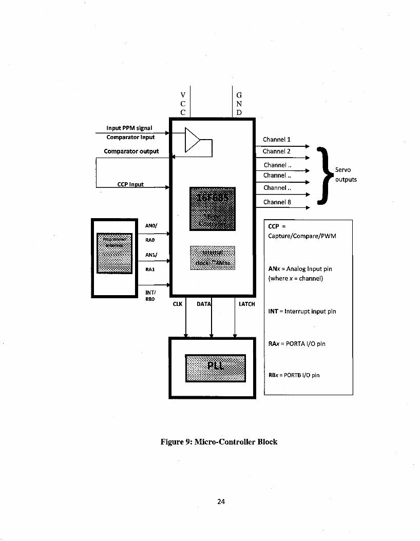
For the design of the receiver a Microchip 16F685 micro-controller was used. A block
diagram of the micro-controller with external interfaces as utilized in the receiver design
is presented in Figure 9. This micro-controller has the following key properties that were
instrumental in its selection [15]:
• Precision internal oscillator: up to 8MHz, this internal clock provides a
stable time base with low jitter. The receiver clock was configured to run
at 4MHz, this enables low power consumption and greater stability and
22

provides more than enough processing capacity. An internal oscillator also
saves a micro-controller pin which can be used as an output servo
controller pin.
• Wide operating voltage: the micro-controller has a wide operating
voltage of 2.0V-5.5V. The receiver powers up the micro-controller at
3.3V, however, the wide operating voltage provides enough margin for
momentary dips in the supply voltage.
• Analog comparator module: the micro-controller features two built-in
analog comparators. The receiver utilizes one comparator to convert the
baseband output of the receiver into a TTL (0V-3.3V) pulse that can then
be further processed by the micro-controller. The comparator features on-
chip regulated programmable and fixed voltage references along with
externally accessible input and outputs.
• Two internal timers: the two internal independent timers provide multi
tasking capabilities.
• A/D Converter: the micro-controller features 12-channels of 10-bit
resolution A/D converters. The receiver utilizes two channels of this A/D
for interface to the external programmer.
• Capture Compare Port (CCP): the CCP port provides 16-bit capture
resolution and has its own internal timer. The output of the internal
comparator is fed to the CCP through an external loop-back.
23
V c c
G N D
Input PPM signal
Comparator Input
Comparator output
CCP Input
Programmer
Interface
ANO/
RAO
A M /
RA1
INT/ RBO
16F685
Microcontroller
Internal
clock: ~4Mhz
CLK DATA
Channel 1
Channel 2
Channel..
Channel..
Channel..
Channel 8 •*
Servo
outputs
LATCH
CCP =
Capture/Compare/PWM
ANx = Analog Input pin
(where x = channel)
INT = Interrupt input pin
RAx = PORTA I/O pin
RBx=PORTBI/Opin
Figure 9: Micro-Controller Block
24

• In-Circuit Serial Programming (ICSP): The ICSP feature allows the
micro-controller to be placed on the PCB without the final firmware
programmed. The micro-controller can be programmed in-circuit after the
product is fully assembled. This also allows field-programmability in the
event that new features are added to the product or for operational bug
fixes.
• 17 I/O Ports: the micro-controller has 17 I/O pins. The receiver utilizes
all of these 17 I/O ports.
The micro-controller provides the intelligence to the products and performs the following
functions:
• Programming the PLL.
• Accept user commands via the programming interface.
• Process the baseband frame and establish the signature of the transmission
over a long interval.
• Make decisions on the validity of the incoming baseband frames based on
the initial signature calculations.
• Decide on the steps to take in case the radio link is severed.
• Drive the servos.
The micro-controller offers a combined user-interface and ICP (In-circuit Programming)
port to download new firmware loads.
25

4.3 Antenna Section
The antenna section of the receiver consists of a bandpass filter. The frontend antenna
filter works as a band-select filter that also reduces image band signals and avoids
frontend saturation [13]. The center frequency of the filter is around 70MHz and provides
a decent cut-off at higher and lower frequencies. Due to the dual-conversion of the
receiver, the main objective in the implementation of the receiver is to provide enough
attenuation to out of band RF radiation so that the mixer saturation is avoided. The
bandpass filter also provides a matching circuitry to the mixer input port and the antenna
(assumed to be 50ohm) for maximum power transfer. The output port is connected to the
MOSFET mixer. The circuit as implemented is presented in Figure 10.
50 Ohm
33pF 120 Ohm
-AAA. 100pF
180nH
50KOhm
Figure 10: Antenna Circuit
26

The circuit was simulated in RFsim.991 package and the results are presented in Figure
11. The simulation results show the performance of the filter, the maximum energy
transfer happens in the 70MHz band, the filter provides sharp cut-off for frequencies
lower than 70MHz where the main image frequencies lies. Above 72MHz, the filter
provides decent attenuation, since the receiver uses a dual conversion super-heterodyne
architecture with a low-IF, image frequencies don't lie in frequencies greater then
70MHz, hence the filter's contribution is to reduce out of band energy above 70MHz to
reduce the frontend mixer saturation.
74.09MHz
10MHz 20MHz- 40MHz 60MHz 80MHz 100MHz 200MHz 400MHz 1 *
Figure 11: Antenna Circuit Simulation, S12 (Log Scale)
1 RFSim99 is a linear S-parameter based circuit simulator offering schematic capture,
simulation, 1 port and 2 port S-parameter display. http://l01 science.com/RFSim99.exe
27

4.4 LO Generation
There are various methods to synthesize a waveform of a certain frequency, the authors
of [6] discuss comparative details of different synthesis techniques and the pros and cons
of each method. Phase Locked Loops (PLLs) are extensively used in the electronics
industry for frequency synthesis, clock and data recovery, and clock de-skewing [12].
Today's high performance PLLs are a preferred choice for wireless communication due
to their stable performance, low noise and tunability [40]. The receiver has to offer
excellent sensitivity in excess of -lOOdBm and cover over 80 unique channels that are
divided over two bands covering a range of 4MHz, this naturally lends to the utilization
of a PLL for frequency control. The LO generation system in the receiver consists of a
low noise VCO that is controlled by a PLL, the following sub-sections will go into details
of these two components.
4.4.1 VCO Section
The receiver VCO utilizes an NPN transistor in a Colpitts configuration to generate the
LO for the first MOSFET mixer. Since the LO is taken from the collector of the
transistor, the Colpitts configuration is preferred because the design inherently isolates
the resonator from the load [36]. A hyper abrupt varactor diode is used to fine-tune and
control the frequency of oscillation through the PLL charge pump output. The hyper
abrupt family of varactor diodes provides linear voltage versus capacitance characteristics
with decent Q and a wide tuning range [36]. The MMBV609LT1 varactor diode used in
the receiver VCO is a dual configuration hyper abrupt diode with a Q of 500 at 70MHz
28

[37]. The gain of the VCO (Kvco) was measured on the bench and was found to be
lOMHz/Volt. The VCO circuit schematic is presented in Figure 12.
vcc From PLL
Charge Pump V Output
0.1uF
VARACTOR
LO for 1st Mixer
180nH
PLL Feedback Input
>
Figure 12: VCO Circuit Schematic
29

4.4.2 PLL Section
The PLL section provides the frequency agility which is achieved through the
combination of the R and the N counter. The R counter divides the input reference signal
by its integer value, similarly the value of the integer N counter is used to divide the
output of the VCO. The outputs of the two dividers (R & N) are fed to the Phase
Frequency Detector (PFD), which generates a current through the charge pumps which is
proportional to the phase difference of the two input sources. This PFD output is then
passed through the loop filter and is used to control and correct the VCO [41].
The basic block diagram of the PLL is presented in Figure 13 [41]. The PLL compares
the VCO output to a known reference signal and the result of the comparison is low pass
filtered and used to adjust the VCO output to increase or decrease the output frequency
[8] [10] [19].
The architecture of the PLL, the design, simulations and phase noise performance and the
unique phase noise minimization techniques employed in the receiver will be presented in
the following sub-sections.
30

Fout
Loop Filter
Phase Detector/ Charge Pump
Figure 13: PLL Block Diagram
4.4.2.1 Phase Lock Loop (PLL)
The receiver utilizes an Analog Devices ADF4001 PLL. This PLL offers very low phase
noise, some of the properties of this PLL are [18]:
• Minimum RF Input Frequency @3V: 5MHz
• Maximum RF Input Frequency @3V: 165MHz
• Minimum Reference Input: 5MHz
• Maximum Reference Input: 104MHz
• Ultra Low phase noise: Typical performance (200MHz) of -99 dBc/Hz at
1kHz offset, 200kHz PFD (Phase Frequency Detector)
• Precision charge pump control
• Low noise digital PFD.
• Analog and digital lock detect
31

• Programmable 14-bit reference divider
• Programmable 13-bit N counter
• 3-wire interface for external programming interface
The block diagram of the PLL is presented in
Figure 14 [18]. The schematic of this PLL as implemented is presented in Figure 15.
CLK(
DAIAt
«FMB<
«f„„ m, M u»00 -O———Or
H>
FUNCTIONAL BLOCK DIAGRAM Vp CPOND O -O
M-SIT INPUT HESBTEH
Mou,
t>
ST L ^ N . JHTER /
FUHGT»« UffCH
NCOUNTER LATCH
PHASE
DETECTOR
m LOCK DETECT
%r ~-o-~
*-QCf*
r~r~FTT~7 cpa cpi2 cm CPIB cm CPM
t t f
Figure 14: ADF4001, Block Diagram
32

Charge Rirp CUputto
\£0
Figure 15: PLL Schematic
4.4.2.2 Phase Noise Reduction
One of the most crucial performance specification of a PLL is the measure of its phase
noise or jitter [8]. Phase noise is the frequency-domain measurement of the noise
spectrum around an oscillator signal, while jitter is the related to the cycle-to-cycle timing
accuracy of the oscillator period [9] [41]. The phase noise of the PLL directly affects the
performance of the receiver, the detrimental effect of increased phase noise on receiver
33

sensitivity and adjacent channel selectivity is well documented in the literature [5] [19],
this phenomenon can also be observed quite easily in the lab with the right setup. There
are various contributors to the PLL phase noise, e.g. PLL N divider, comparison
frequency, PLL 1/f noise, charge pump gain, VCO noise, TCXO noise, etc. [41]. The
authors of [10] and [41] discuss in detail the effects and contributions of each of these,
however, the PLL N divider plays the pivotal role and is the main contributor to the final
phase noise figure [19].
In a PLL, one input to the phase/frequency detector (PFD) is the reference oscillator
signal divided by the R counter [19]:
The second input to the PFD is the VCO output divided by the feedback N counter, at
equilibrium the two inputs are equal and the LO output is [19]:
FLO = N * FPFD
As per the above equation, the N numbers are inversely proportional to the FPFD [41].
The phase noise of the PLL is multiplied up from the PFD at a rate of 20*log(N) [10]
[19] [41], reduction of N by a factor of 2 improve system phase noise by 3dB, hence the
lowest N values should be used [19].
A 25MHz T0521 low phase-noise precision TCXO (Temperature Compensated Crystal
Oscillator) clock is used to generate the reference input to the PLL [38]. The reference
TCXO was determined using the standard available TCXO frequencies and calculating
the N numbers using the algorithm presented in the Figure 16. The 25MHz reference was
determined to give the lowest maximum N number and also the lowest average N
34
numbers for the entire range of operation. This TCXO offer excellent stability and
tolerance of less than +/-2ppm over a temperature range of -20C to +70C, the phase-noise
performance of the TCXO is -135dBc/Hz @ lkHZ offset [38]. A good frequency
reference with low phase noise is critical for stable PLL performance and ultimately the
performance of the receiver [19]. The T0521 TCXO offers a clipped sine output which is
preferred for low phase noise PLL operation since sharper clock edges result in less jitter
at the R divider output [19].
The receiver requirement is to cover 80 channels in two bands (72/75 MHz), in each of
the bands individual channels are contiguous with a difference of 20kHz. To cover the
entire band the highest FPFD according to conventional techniques would have to be
10kHz, this would result in the smallest N value of around 6100 (N = — ^ = - ) . A V FpFD lOfcHz7
PLL with this high N value would increase the LO jitter and reduce adjacent channel
selectivity which would render the receiver unusable in a crowded RF environment.
To reduce the N numbers, a different technique was followed whereby an iterative
computational method was formulated which for each channels starts with the lowest N
value and increases the R divider until a LO frequency is achieved that has the smallest
difference (error) from the real LO frequency. The flowchart of the algorithm is presented
in Figure 16, the algorithm was coded in C. The resulting N numbers distribution is
presented in Figure 17 and shows that for majority of the channels the N numbers lie
between 300~600, the smallest N number was less than 100, while the highest N number
35

was not greater than 1300. It is clearly evident that even for the worst case N number
derived from this method, the reduction is almost 4 times compared to the best case N
number of the conventional technique. This is almost 6dB reduction in phase noise as
per: 10*log(4) [19]. The downside of this method is that for a majority of the frequencies
the LO has an offset error, it was experimentally determined that the receiver can easily
tolerate an error of ±1.5kHz in the LO frequency as long as the spectral purity is
maintained. The distribution of the offset error for each channel is presented in Figure 18.
For the majority of the channels the offset lies between ±300Hz, the maximum error is no
more than ±lkHz, which is well within the error limit of ±1.5kHz determined
experimentally.
36

Begin
Select the First Channel
Frequency
Select the smallest N = 3
multiplier number
Select the smallest divider R =1
Figure 16: Flowchart for calculating PLL Phase-Noise optimized N numbers
37

93 ™, 22 -21 -20 -19 -18 -17 -16 -15 -
S" 14 -c 13 -SJ 12 -g- 11 -« 10 -£ 9 -
8 -7 -6 -5 -4 -3 -2 -1 -0 -
Histogram of the N Numbers for SL-8
° ̂ # # > c? >#
HI 5 • • • ill _ 1 | ____•__
N Number bins
Figure 17: Histogram of the N numbers for the receiver
19 -,
n -10 -
9 -
8 £T 7 -c '
cr S 5 U_
O
T
1
Histogram of the LO error for SL-8
l 1 1 T
1 I
"T I T" "T ~i ____ m
o o o o o o o o o o o o o o o o o o o o o o o o o o o o o o o o o o o o o o o o o o o o o riooiMNiiJui^mNri i - H ( N m ^ - m i o r - . o o a i o * n TH I H I " i ' H ri
1 1
Error in Hz
Figure 18: Histogram of the LO error for the receiver
38

4.4.2.3 Loop Filter Calculation
Various studies have been conducted on the optimal loop filter design as presented in [2],
[39], [40], and [41]. For the receiver implementation, we primarily follow the techniques
presented in [40] and [41].
The PLL Loop filter is a critical section of the PLL. The biggest contributors to the phase
noise of the LO are the VCO and the noise generated by the PLL components, e.g.
reference dividers, phase detector, multipliers, etc. [41]. To understand the effects of the
loop filter and how to arrive at an optimum design, we will look at some basics of this
section of the PLL. Referring to Figure 13, PLL transfer functions are defined as [40]
[41]:
Forward Loop Gain = G(s) = K^Z^s)-^-^ = 2njf; K^ = Charge pump Gain
1 Reverse Loop Gain — H(s) —T:'>N = PLL N Numbers
IS
Open Loop Gain = H(s).G(s) = K^Z^s)-^- ; \H(s)G(s)\ = 1 v Ns
The VCO transfer function as stated below is determined by introducing a test frequency
at the input and observing the corresponding change in the output frequency [41]:
VCO transfer Function = [1 + G(s)tf(s)]
The close loop transfer function takes into account the whole system:
G(s) Close Loop Transfer Function (VCO + loop filter) =
39
[l + //(s)G(s)]

The transfer function of the loop filter is defined as the change in voltage at the tuning
port of the VCO divided by the current at the charge pump that caused it:
l + sT2
sA0(l + sTl) Transfer function of a PLL loop filter (2nd Order) = Z(s) =
CI Tl = R2C2-; T2 = R2C2; AO = CI + C2
The phase noise of the system with a very large PLL loop bandwidth is dominated by
noise of the PLL, while in a very narrowband loop filter it is dominated by the VCO
noise [2] as depicted in Figure 19 and Figure 20. This presents a tricky situation and
careful analysis of the end application is used to determine the optimal bandwidth of the
system. In most PLL system, a very low phase noise reference is utilized and thus the
VCO noise is a major contributor to the overall Phase noise [2]. Increasing the loop filter
bandwidth may seem like a simple solution, However, increasing the loop filter
bandwidth also increases the spurious noise due to reference spurs [41] [42] and too wide
a bandwidth can also cause the loop to become unstable and lose lock permanently [19].
Frequency 0)C = PLL Loop filter bandwidth
Figure 19: Noise contribution of all sources except VCO [41]
40

0 C = PLL Loop Filter Bandwidth
Figure 20: Noise contribution of the VCO [41]
• • Frequency
Another consideration in the loop bandwidth as per the loop filter transfer function is that
if it is too wide the loop filter capacitors become very small and can be swamped by the
parasitic capacitances and the VCO input capacitance, similarly, for too narrow
bandwidths the loop filter capacitor becomes unrealistically large [41] [42]. For the PLL
loop filter a typical bandwidth of 10kHz was chosen for the design based on tests
conducted on the bench which included subjecting the receiver to vibration stress and
measuring the LO stability.
The stability of the PLL is dependent on the PLL phase margin (<p), it is specified as the
difference between 180 degrees and the phase of the open loop transfer function:
<p = 180 - z.G(5)//(s)
41

Typical values range between 40 to 45 degrees [41]. As per [40] the phase margin for the
calculations was selected to be 45 degrees to produce an optimum settling transient of the
PLL [19], an example diagram of a PLL settling transient is shown in Figure 21.
iiJMMHz
Figure 21: Settling Transients
A second order passive PLL loop filter was selected as shown in Figure 22 [40], this was
done for simplicity in terms of number of components and also because of very wide
variation of loop gain for our design due to large variations in the N numbers across the
band. Since lower order filters are more immune to changes in the loop gain compared
to higher order loop filters, it is suggested that if the loop gain varies by more than a
factor of two, a lower order filter should be considered [41]. As presented earlier, the
42

design uses a wide variation of N numbers, this fact becomes a deciding factor in
choosing a second order passive loop filter.
Do 1 1 VCO
CI T I
Figure 22:2nd Order Passive Filter
An active loop filter was another option which was not considered due to inferior phase
noise performance, added cost and complexity [41].
The charge pump gain (K^) was selected to be 3mA, this was selected as a first pass
estimation and high enough to minimize charge pump leakage effects. As presented
previously the PLL loop bandwidth gain is directly proportional to the charge pump
current, also the bandwidth of the loop filter is inversely proportional to the N numbers.
As per section 4.4.2.2, N numbers in the design vary quite a bit, for a low N number
channel the bandwidth of the loop filter decreases and to bring it back in the vicinity of
the 10kHz design target the charge pump current is also reduced. For channel frequencies
with high N numbers the bandwidth of the loop filter is reduced and a higher current
setting is utilized to bring the bandwidth within the design margin. The final charge pump
values for each discrete frequency were selected based on the bench performance.
43

The PLL N numbers were calculated before the loop filter design and the highest N
number (1227) was selected for the design specification after experimental tests with
respect to the observed phase noise.
Figure 23 below presents all the design specifications that were used to calculate the loop
filter components.
Symbol
h
a)p
<P
K(p
"•VCO
N
Description
Loop B a n d w i d t h
di-p-2 .71.Fc = Loop
b a n d w i d t h i n
r a d i a n s
P h a s e M a r g i n
C h a r g e Pump G a i n
VCO G a i n
PLL N Number
V a l u e
10
6.283xl04
45
3
10
1227 (MAX)
Units
kHz
r a d / s e c
d e g
mA/2Ttrad
M H z / V o l t
-
Figure 23: Design Specifications for the 2nd Order Loop Filter
44

Based on the above presented design specifications, time constants Tl and T2 which
determine the frequencies of the pole and the zero of the filter transfer function were
calculated as per [40] [41]:
Tl = s e c ( y ) - t a n W = 6.594X10"6 sec up
T2= —±— = 3.8423xl0~5 sec "P
Calculation of the three loop filter components were done as per:
C l = ^ S ! f e i i ^ ! = 2 .56nF
C2 = C1 . (—- 1) = 12.38 nF v r 2 j
R2 = — =3.1kQ C2
The above circuit was built and found to give excellent performance for all frequencies.
The final values as shown in Figure 15 were determined taking into account standard
component values and also with some minor bench work tweaks applied:
CI = 2.2nF, C2 = 15nF, R2 = 2.7kH
4.5 First Mixer
Mixers are designed to translate signals from one frequency to another. They have two
inputs and one output as shown in Figure 24
45

Mixer
Input: RF J J L •Output: IF
Local Oscillator
Figure 24: Mixer Block Diagram
The mixers in receivers are generally called down-converting mixers due to the fact that
they take an information signal on the input (RF) at a certain frequency, and shift it to
another frequency and present it at the output (IF), to do so they are fed a large periodic
Local Oscillator (LO) signal, the frequency of this LO signal equals the amount of
frequency translation desired, a mixer thus behaves both linearly to the RF input and
strongly non-linear to the LO input [29]. Traditionally Schottky diodes have been the
most non-linear device for mixers, however, the field-effect-transistors (FET) devices
have become more popular due to low noise performance, high conversion gain and low
LO requirements [11].
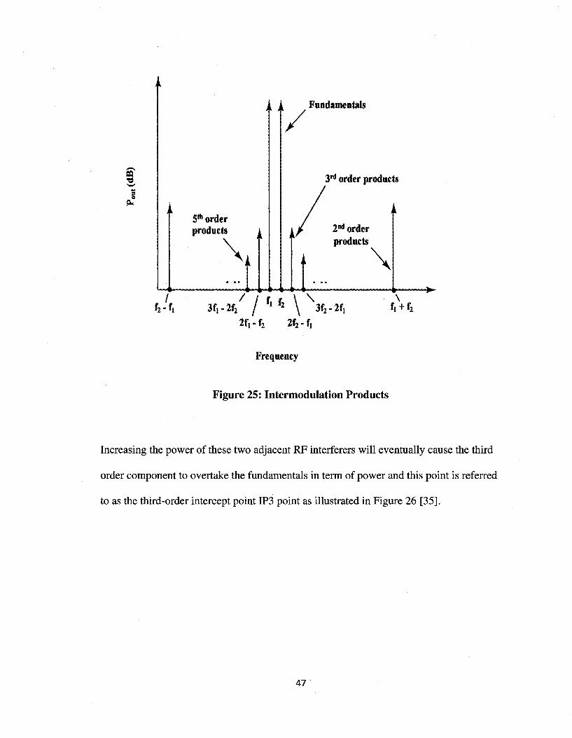
One of the most important performance parameter of a mixer is the third order
Intermodulation distortion point (30IP). In a system like 72MHz RC band where equally
spaced channels are used, two adjacent RF sources can generate undesired components
that are sum and differences of the multiples of the fundamental frequencies of these
sources inside the mixer [35]. Most of these components are out of band and hence cause
no major issues, however, the third order tone is on the fundamental and adds non-
linearity and distortion in the output as presented in Figure 25 [35].
46
i
/
5th order products
\
4 » » »
Fundamentals
3rd order products
2nd order products
\
/ fi-fi 3fi-2f2 / fl k \ 3f2-2f!
2f2-fj
/
2f,-f2
\ fi + fi
Frequency
Figure 25: Intermodulation Products
Increasing the power of these two adjacent RF interferers will eventually cause the third
order component to overtake the fundamentals in term of power and this point is referred
to as the third-order intercept point IP3 point as illustrated in Figure 26 [35].
47

09 it«3
3rd Order Products (slope = 3:1)
2nd Order Products (slope = 2:1)
Fundamentals (slope = 1:1)
Input power = Pfa(dBm)
Figure 26: Third Order Intercept Point (IP3)
The first mixing stage of the receiver is realized with an N-channel dual gate MOSFET.
The BF908WR MOSFET offers high forward transfer admittance, low-noise gain and a
maximum noise figure of 2.5dB @800MHz [16]. The RF input through the antenna
section is applied to the gatel of the MOSFET, the LO (local oscillator) input is applied
to the source and gate2. The resultant 10.7MHz IF is generated at the drain port of the
device. The schematic of the MOSFET mixer as implemented is presented in Figure 27.
This topology offers very high linearity and excellent Third-Order Intermodulation
(30IP) performance in excess of +5dBm based on comparative measurements with
commercial receivers.
48

The dual gate MOSFET provides an inherent separation of LO and RF ports and allows
both of these ports to be separately matched for maximum power transfer [11]. The dual
gate MOSFET can be considered equivalent to a cascade of two single gate MOSFETs,
the LO is applied to the upper FET, while the RF is applied to the lower FET [11]. When
the LO signal is applied to the gate of upper FET it goes into saturation region while the
lower FET remains in the linear region, the mixing process takes place in the lower FET
while the upper FET acts as an amplifier [11].
49

WK*»
Output IF
input t o : : " *
Input RF
Figure 27: MOSFET Mixer Schematic
The LO frequency is generated according to the principles defined in the PLL section,
and is always at an offset of 10.7MHz from the RF of interest.
50

4.6 10.7 MHz IF Section
The first IF filter (10M05B) is custom designed four-pole monolithic crystal filter
(MCF), it is based upon the lOMxxB family of MCF [33]. This filter has a bandwidth of
5kHz @ 3 dB, stop bandwidth is 22kHz (around the centre frequency) and a minimum stop
band attenuation of 50dB. The schematic of this section is presented in Figure 28.
10.7MHz Input ;:::.:::::v:,.. :.;::W:i 3 ^ r C h ' : ^ v , ; - i l i ' . : .3 , n 7 U U ~ . . r ;,.,.,,,„,.ta ; ;:;.:fa—•S> ^MfejU^jJL.:,;.^^. a^/S/%^-—~ 1 ( ) . 7 M H Z O u t p u t
r r o m Mixer ste&fcv-ia'l ;:: isfe: *—»_ *u^> mi/->c
Figure 28:10.7MHz IF section
4.7 Limiter Section
The 10.7MHz section also incorporates an AGC/hmiter circuitry. The AGC apparatus
consists of a transistor that is controlled by the RSSI signal output from the second IF
mixer, the transistor attenuates the 10.7MHz signal going into the 2nd Mixer based on the
RSSI feedback as presented in Figure 29. The second mixer utilized in the design is a
Toshiba receiver IC (TA31136), the RSSI signal of this device provides a linear range of
about 80dB [17].
The limiter circuitry provides attenuation of high IF levels and also lowers the Third
Order Intermodulation Product (IP3) levels of the second mixer. It should be noted that
the IP3 performance of the first stage mixer is exceptional (+5dBm), however the second
51

IF mixer has an IP3 point of -1 ldBm which is much lower comparatively [17]. In the
case of this receiver implementation, the limiter provides a gain of ~6-7dBm in regards to
measured IP3 improvement.
10.7MHz output of the MCF
RSSI Signal Input from 2nd Mixer
Figure 29: Limiter/AGC Circuitry
4.8 Second Mixer (IF)
The second mixer take the 10.7 MHz IF and further downconverts it to a 455kHz IF. An
integrated FMIC TA31136 from Toshiba is used as a second mixer, it provides a
compact SMT package, very high sensitivity of -96dBm, low operating voltage (1.8v-
5.5V) and an integrated quadrature detector for baseband recovery [17]. The schematic of
the second stage is presented in Figure 30.
52

I 31
Si Er v
3
1 if
Figure 30: Second Stage Mixer, IF and Demodulator Stage
53

The LO port of the mixer is fed from a fixed crystal oscillator at 11.155MHz. The
resultant output of the mixer is amplified internally and baseband filtered through a
cascade chain of two external IF filters. A built-in quadrature detector in conjunction with
an external ceramic discriminator provides the baseband signal.
4.9 4 5 5 kHz IF Section
The second IF filter (CFUKG455KH1X-R0) is a cascade of two SMD 4-pole ceramic
crystal filters operating at a centre frequency of 455kHz and a 6dB bandwidth of 6kHz,
the stop bandwidth is 20kHz within 40dB as depicted in and Figure 31 [23].
100 442 455 Frequency (kHz)
46$
I-: Q
6
Figure 31: CFUKG455KH1X-R0 Frequency Characteristics (narrow-band)
54

4.10 Discriminator Section/Baseband Recovery
The baseband is recovered by a 455kHz ceramic discriminator (CDBKB455KCAY07-
R0) that offers a recovered signal bandwidth of 4kHz and an output level of 350mV, the
frequency characteristics of this discriminator are presented in Figure 32 [23].
500
100
§0
I 1 10
1
440 450 460 470 Frequency (kHz)
Figure 32: CDBKB455KCAY07-R0 Frequency Characteristics
4.11 Programmer Interface
The Programmer Interface on the receiver allows the user to modify and select the
following options [20]:
\ t
50.0
10.0
5.0
1.0
0-5
0.1
q
55

• Change the frequency of operation.
• Change the Failsafe options.
• Change the mapping of the logical channels to the physical pins.
• Enable/modify other options of the receiver, e.g. enable/disable the digital signal
processing of the incoming frames, reset the receiver, etc.
The programmer consists of two ITT Cannon 10-position BCD encoded DIP rotary
switches and a pushbutton as depicted in Figure 34 and Figure 35. Each rotary switch has
ten positions that are selectable by the user and five contact terminals; one terminal is
common, while the other four form connections depending on the switch position as per
Figure 33 [48]:
FOS. w
1 2 4
S
0 •
1
•
•
2
•
•
3 m •
m
4
•
•
5 •
•
•
6 •
#
•
7
•
•
•
•
a •
•
9 •
•
•
Figure 33: Rotary BCD Switch Connections
The two rotary switches are connected to two independent but similar resistor networks
that provide a unique voltage output for every switch position. It should also be noted that
the programmer is a completely passive device with no active components. The receiver
56

supplies the power to the programmer unit when it is connected through the programmer
port.
Figure 34: Programmer
&3V
a»
F»> R3& R2> R l i 1K87 ? 4K02 ? JKS1 ? *SK?
PUSH 8MTT0S SWtTCH
O700 44.
LED
SCO ROTAfW SWITCH
B„1 4 COMMON M5SJ8
• • T G A B «
RO 1KB?
Figure 35: Programmer Schematic
Switch 2 implementation is exactly like Switch 1
57

On the micro-controller side the output of the resistor network is connected to analog
inputs that can measure the voltage output. When the pushbutton of the programmer is
asserted, it signals the micro-controller to sample the voltage present on the output of the
two resistor networks and hence a unique code is registered by the micro-controller. This
scheme allows the use of only three pins, however, it results in a very precise and
accurate method to achieve 100 unique steps. A comparable digital (binary) method will
consume 7 micro-controller pins [20].
The main challenge in the design of the programmer is to keep the output voltage such
that every position of the rotary switch results in a unique voltage output that can be
sampled by the micro-controller without any ambiguity. A minimum voltage separation
of lOOmV was selected as a design criteria, this value was selected to achieve a resistor
network design with commercially available values that can give 10 unique voltage
outputs for a Vcc of 3.3V and also provide a large enough separation between two switch
positions such that noise, etc. cannot result in a false reading.
The resistor network schematic as presented in Figure 35 was determined by utilizing an
exhaustive iterative program written in C. 100 commercially available resistor values in
the range of IkQ. to 33k£2 with 1% tolerance were defined, the smallest resistor value
from the list was selected at the start of the program and the 10 voltage outputs were
calculated for every possible resistor value combination for the rest of the network as per
the following set of equations which were derived taking into account the rotary BCD
switch configuration as per Figure 33 for each position. Voltage V0 represents voltage
output for switch position "0", etc.:
58

V0 = OV; V1 = Vcc*-^-\V2 = Vcc*-\-;V3 = Vcc* § , ° ' 1 CC RQ+RI> ' CC Ro+Rz 6 CC R «^_+B '
RQ+R2
v4 = Vcc*nJ^;Vs = Vcc*ri «: in;Ve = Vcc*ni £ |C ,
v7 = ycc* B .^ frL ,^ ; v8 = vcc*-^--, Vo = vcc * R
7 ~ CC Rl*
R2*Rz*iRz+R3\Ro 8 ~ CC Ro+RS 9~ CC R^T^T+RO
n i (R2+R3)*R2*R3 ° * Rl+R4 °
The 10 voltage outputs at every step were checked to make sure that the minimum
separation criteria of lOOmV is satisfied. A flowchart depicting the complete algorithm is
presented in Figure 36.
The iterative algorithm as presented gave the following resistor values and switch position
voltages:
RQ = 1.87KH; R± = 13tffl; R2 = 7.51^X2; R3 = 4.02^0; R4 = 1.87KD.
V0 = Ov; V1 = 0.4l5v; V2 = 0.658V; V3 = 0.931r; V4 = 1.047i7; V5 = 1.249x7;
V6 = 1.375x7; V7 = 1.524t7; V8 = 1.658t7; V9 = 1.76v;
From the above it can be seen that the nominal voltage difference between two adjacent
switch values is:
V1- V0 = 0.415x7; V2-V1 = 0.243x7; V3 - V2 = 0.272x7; V4 - V3 = 0.116x7;
V5 - v4 = 0.20117; V6- V5 = 0.126x7; V7 - V6 = 0.149x7; V8 - V7 = 0.125v;
V9-Va = O.llv;
59

f BEGH ^ P f " ' 600
610
INPUT ROUST OF WESfSTOR VALUE
8ELECTNEXT VALUE FOR fSI
A » coupon vi
J TL 60S
;YES
SORT NEXT VAUJE FOR m. AND
COMPOTE WAND V3
SELECT MBCT VALUE FOR R3 AND OOMPU1E ¥4, VS» W, V7
mmi M©cr VALUE FOR M AND COMPWF1V8 AND ¥9
SUCE83LSOUJTION S6TF0W0
fPRINT AU. THE SOLUTION SETS FGUMP | S ( S T O P )
Figure 36: Programmer Resistor Calculation Flowchart
60

Since the resistors used are commercial 1% tolerance, a further analysis was conducted to
analyze the performance of the circuit taking into account worst case drifts in the resistor
values. 256 worst case combination scenarios were simulated and the following results
were obtained.
Maximum adjacent switch position voltage difference for worst case resistor drifts:
V1-VQ = 0A22v; V2 - Vx = 0.254v; V3 - V2 = 0.277t?; V4 - V3 = 0.123v;
V5 - V4 = 0.205v; V6- V5 = 0.131v; V7 - V6 = O.lSlv; V8 - V7 = 0.134v;
V9 - V8 = 0.112i;;
Minimum adjacent switch position voltage difference for worst case resistor drifts:
V1-V0 = 0A07v; V2-Vx = 0.233v; V3-V2 = 0.267v; F4 - V3 = 0.102r;
V5 - V4 = 0.198v; V6 - V5 = O.Ulv; V7 - V6 = 0.147v; Va - V7 = 0.113t;;
V9 - V8 = 0.109y;
From the above analysis, it is evident that the design is robust given 1% tolerance
resistors are used.
61

5 Baseband Signal Processing
This section describes in detail the baseband decoded signal, the protocol and framing
utilized to encode information, and servo output calculation according to an auto-
regressive smoothing filter. Details on comparator based baseband signal conditioning,
and the search algorithm utilized to determine the nature of the frame are also illustrated.
5.1 PPM Frame Protocol Basics
The transmitter reads the information from the control switches and joysticks as a Pulse
Width Modulated (PWM) signal. The PWM signals from all the switches and sticks are
multiplexed together serially to form a Pulse Position Modulated (PPM) frame. The
width of the frame is a fixed duration of 22.5ms; this translates into an output frame rate
of45Hz.
There are two industry standards for encoding the frames, one is called positive shift,
where the information is encoded with a voltage that is more than ~2.0V. The negative
shift signal encodes information with a voltage level that is closer to OV and is usually
~0.1V. These voltages can change depending on the number of encoded channels, sync
pulse width, and the frame rate. However, the voltages in either shift remain within the
above-mentioned nominal range.
In a positive shift framing system, there is a variable high phase and a constant low-phase
that is around 0.3ms wide. The negative shift frame is the exact opposite of the positive
shift, instead of a constant low-phase (0.3ms), it has a constant high-phase (0.3ms). The
variable part of the pulse is low-phase. Due to this difference, the positive and the
negative frames have different DC offsets.
62

Figure 37 shows the structure of the positive and negative shift PPM frames.
h- Sync Pulse
M Sync Pulse — W
Positive Shift Frame (PPM)
Servo Pulse 1 (PWM)
Negative Shift Frame
Servo Pulse 2 (PWM)
Figure 37: Positive and Negative Shift PPM Frames
The receiver processes a frame and outputs proper control pulses to the servos. The servo
position information is PWM based, the width of these pulses define the servo positions.
Output servo pulses can range from a minimum of 1ms to a maximum of 2.0ms, middle
position is 1.5ms. The sync pulse width depends on the number of encoded channels, rate
of transmission and the current position of the servos. The sync pulse is always greater
than the maximum possible servo pulse width (2.0ms). Minimum sync pulse is 2.5ms,
this corresponds to a case of 10 encoded channels in a frame.
During the course of normal operation, the sync pulse varies from frame to frame
depending on the current servo position, e.g. in an 8-channel transmitter system the sync
pulse can vary between 14.5ms (all servo positions are 1ms) to 6.5ms (all servo positions
63

are 2ms). Figure 38 shows a positive shift PPM frame with 8 channel servo positions and
the decoded servo PWM signals.
f»P«»Praie •22,5 ns-
rSyncMse ~*\ lis | 1 K | I , & » |
start in unjTunn Lfi¥ruru
Decoded PWM Servo Outputs
SyiK
1 PWM Servo Pulse #1 (2ms)
PWM Servo Pulse #2 (1ms)
3 I PWM Servo Pulse #3 (1.5ms)
m PWM Servo Pulse #8
Figure 38: Positive Shift PPM frame and Servo Decoding
Following is a summary of some basics of PPM frames:
Frame width: - 22.5ms (~45Hz)
Servo pulse (low-extreme): ~ 0.92ms-1.0ms
Servo pulse (high-extreme): ~ 2.0ms-2.12ms
Servo pulse (neutral/middle stick): ~ 1.5ms-1.52ms
Maximum number of channels in a transmitters: 10
Minimum number of channels in a transmitters: 3
• Minimum width of sync pulse: 2.5ms (based on 10 channels)
64

5.2 Comparator Section
The decoded baseband signal is an AC signal superimposed on a DC signal. Since the
micro-controller is a digital device, the incoming baseband signal needs to be conditioned
and transformed any further digital processing so that the high and the low phases are
accurately determined. A built-in internal comparator of the micro-controller is used to
achieve this. The incoming baseband signal is connected to one input of a comparator of
the micro-controller, the other input is connected either to internally generated 0.6V for
the negative shift frames or 0V for the positive shift frame. The output of the comparator
generates a TTL (0-3.3V) version of the incoming PPM frame as shown in Figure 39.
3.3V
ov
Decoded negative shift baseband signal
TTL conditioned output of the comparator
3.3V
Decoded positive shift baseband signal
0.8V
-0.2V
Figure 39: Baseband Conditioning and Comparator Output
65

5.3 PPM Frame Search Procedure
The receiver boot-up sequence consists of programming the PLL; once the PLL is
programmed the micro-controller analyzes the content of the baseband signal. The
complete boot-search sequence is presented in Figure 40 [20]. The comparator toggle
function is instrumental in detecting the shift of the incoming signal. Once the PLL has
been programmed, the toggle is asserted to a value (either high or low) and the micro
controller tries to determine if valid frames are detected in this toggle position. The
toggle remains in one position for around ~500ms, during this time 10 valid continuous
frames should be detected, failing this the toggle polarity is reversed and the same criteria
is applied in an infinite loop until the above-mentioned condition is fulfilled. Once the
condition is satisfied, the toggle is maintained at the same polarity where proper frames
were detected for the rest of the duration of the operation (i.e. until power is cycled or the
receiver is reprogrammed).
66

( BEGIN
f
m
mmwi RESET
m
i
m PROGRAM THE
m FOR PROPER FREQUENCY OPERATION
%#M!#^
SET COMPARATOR \ ) THRESHOLD FOR
NEGATIVE SHIFT PPM
SET COMPARATOR THRESHOLD FOR
POSiTME 8MFTPPII
m
{ UXKCMPCM T SISNWIANDOONIWUE J HOWMLOpewnoiis J
sss
<00K NEGWIVESHIFT P f # T SIGNAL AND CONTINUE } M Q R m DERATIONS J
<L0OK POSITIVE SHIFT P P l \ StGHALANDCOKlMJE J Nowwiopawioiis J
Figure 40: Boot-up Sequence of the receiver
The following criterion defines a valid frame and was used in this procedure:
• The frame is either 20-22.5 ms
67

• The longest low or high pulse (larger than or equal to 2.5ms) determine
the shift of the frame
• Sync pulse cannot be less than 2.5ms
• The number of servo channels should be no less than 3 and no more than
10
• Servo pulses should be within the range of ~ 0.92ms - 2.12ms
Once shift detection and rate determination is completed by the micro-controller, the
following features of the frame are noted for the duration of the operation (i.e. until
power is cycled or the receiver is reprogrammed) and used in subsequent filtering and
processing of the frames, we'll collectively call these the "frame-signature":
• The shift of the frame (positive/negative)
• The rate of the frame (low/high)
• The number of channels
• The consistent high-phase duration (for negative shift) or the consistent
low-phase duration (for positive shift)
5.4 Incoming Frame Filter
The function of the frame filter is to either accept a frame or reject it. Frames can be
rejected due to noise or interference corruptions and are not processed since they'll result
in erroneous undesired outputs on the servo control lines. The following filter is applied
to all incoming frames:
• The frame should match the shift and rate as defined in the "frame-
signature" during the detection phase
68

• The frame should contain valid servo pulses
• The frame should contain valid sync pulse
• The frame should match the number of channels as defined in the "frame-
signature" during the detection phase
• The frame should match the high/low phase duration as defined in the
"frame-signature" during the detection phase
A frame that doesn't pass the above filter requirement is rejected and the previous known
good servo outputs are sent out. The above-defined filter will henceforth be called
"glitch-filter".
5.5 Frame Processing and Servo Output Calculation
Once a frame passes the "glitch-filter", the servo outputs can be read and processed.
Immediately following the sync pulse section, the first pulse in a frame represent servo
position for channel-1, the second pulse contains servo position data for channel-2 and so
on and so forth until the end of the frame (start of a new sync pulse).
To minimize jitter and to provide a smooth servo movement, the following auto
regressive smoothing filter was utilized to calculate the final servo output position:
l(c,x) = 0.75 * tf{c,x) + 0.15 * l(c,x - 1) + 0.10 * l(c,x - 2) + 0.03 * l(c,x - 3) + 0.02 * l(c,x - 4)
c = servo channel number; x = frame number
lie, x) = final servo output pulse width
t(c,x) = servo output pulse width for channel c contained in the current decoded frame
69

5.6 Servo Outputs and Failsafe
Servo outputs as mentioned earlier are Pulse Width Modulated (PWM). The servo
movement transcribes an arc; an output pulse width of 2000us will move the servo in one
extreme position, the other extreme position is achieved with a pulse width of lOOOus.
Neutral is defined as 1500us. The maximum pulse width change is 1.0ms.
Upon power-up the servo output lines are be kept high until valid pulses are ready to be
sent out, this makes sure that no glitches are sent out to the servos during initialization
and detection phase.
In case where the number of transmitted channels in a frame is less than 8, the spare
servo pins are driven low during normal operation (i.e. once boot-up and detection phase
is over).
In a situation where a bad frame is received, previous known good servo outputs are used
to drive the servos. If continuous bad frames are received for 1.5 seconds, Failsafe
condition is activated, whereby all servo outputs are to be driven low, in this case the
ESC (Electronic Speed Controller) will be given a chance to shut-down the throttle to the
motor.
Servo outputs are to be generated for each channel at 45Hz. The latency in processing the
frames and jitter in the output servo pulses was kept to a minimum. Latency in servo
outputs was no more than 20ms under normal circumstances, in the event of frame
corruption latency will go up. Servo output jitter was also no more than 2us.
70

6 Future Research Suggestions
In this research we present a synthesized, high performance, intelligent receiver for
remote control. While this solves a number of issues with the current products available
in the market, it does have inherent deficiencies, and new and upcoming technologies can
further enhance some of the features of this system. The following sub-section will be
categorized according to different research topics that can be investigated further.
6.1 Miniaturization
As presented in the opening sections of this thesis, the size and weight of the receiver is a
major concern for a lot of modern unmanned vehicle applications. Micro UAVs are the
considered one of the most important future warfare component and an indispensible tool
in the arsenal of every soldier [47]. Reduction in the size and the accompanying weight
can mean smaller and lighter vehicle structures towards this development.
There are multiple research opportunities toward this goal of miniaturization as listed
below:
6.1.1 Digital Processing
Most of the real estate occupied on the current receiver PCB is due to the external passive
IF filters, the two downconversion stages, the discriminator and the baseband processor.
One solution to this problem is to digitize the RF with an ADC and perform all the
operations digitally [25]. This however requires ADCs with a large dynamic range and
substantial computational processing power for signal processing. As the authors in [25]
suggest, moving the ADC to IF can reduce the dynamic range requirement of the ADC
and also reduce the processing power requirement of the DSP in the backend.
71

6.1.2 Low-IF Architecture
Earlier we discussed different receiver architectures, we presented homodyne receiver
and its shortcomings. A compromise to the issues faced in a homodyne receiver can be
solved with a Low-IF architecture. The mixer rather than down-converting the RF to
baseband, converts to a low IF (around a few hundred kilohertz), this low-IF can then be
easily processed. Recent advanced in integrating high-performance active filters on-chip
means that this will become a viable alternative to the super-heterodyne architecture in
the near future [3].
6.1.3 CMOS Integration
The bulky passive filters of super-heterodyne receivers can be integrated in CMOS on a
single die along with all other RF front-end and back-end components. The authors in
[21] present a complete dual-conversion FM receiver on a single die, with on-chip
switched capacitor filtering and baseband demodulation. There are a multitude of issues
with this integration and delicate balance of different parameters based on performance
criteria have to be undertaken, however, this is an area which has tremendous potential
for future research. Not only is the superior performance of a super heterodyne receiver
preserved, but the drawback of bulky external filters is also removed in this approach.
Another addition to the integration exercise would be to integrate the baseband
processing and distribution of the control frame on the same chip. Currently an external
micro-controller is utilized to process the incoming baseband and distribute the controls
to the servos or other peripherals. This task can become part of the baseband recovery on
the RF chip. The authors in [7] have successfully demonstrated fabrication of a CMOS IC
72

using VLSI techniques for the replacement of the micro-controller in RC receiver
applications.
6.2 Enhanced Reliability and Robustness
This section will focus on enhancements that can yield more robust RF link between the
controller and the unmanned vehicle. A self-healing, resilient link, along with vehicle
intelligence and autonomy are some of the hottest research areas.
6.2.1 Front-end Filter
For a narrow-band receiver, one of the major challenges is to restrict the out-of-band RF
energy from entering the first stage mixer, this requires extremely sharp and tunable
filters [22]. One area of further research would be to integrate high-Q and very sharp
tunable filters in CMOS, this would not only attenuate out-of-band RF, but also allow a
single receiver to operate in multiple bands.
6.2.2 Spread Spectrum RF Link
Narrow-band operation has the benefit of allowing a multitude of users and the overall
utilization of the spectrum is quite efficient. Narrow-band systems however are more
susceptible to interference and a low SNR [24]. Furthermore, current regulatory
provisions on shared access in 72/75MHz are archaic and require error-prone user
intervention in regards to spectrum access and frequency separation. Lack of bandwidth
in 72MHz also doesn't leave room for any addressing information to be transmitted.
This lack of plug-and-play operation and digital modulation in 72MHz present a
fundamental disadvantage and towards that end the Spread Spectrum access and digital
data modulation techniques offer tremendous benefits. Each transmitter can have a
73

unique addressing ID that is part of the transmitted packet header and only the receiver
with the corresponding ID can decode and recover the packet information to drive the
servos etc.
Spread spectrum techniques utilize more bandwidth, two of the prevailing spread-
spectrum techniques are DSSS (Direct Sequence Spread Spectrum) and FHSS
(Frequency Hopping Spread Spectrum). In DSSS, the transmission data sequence is
multiplied by a special pseudo-random chip sequence that causes the resulting data to
appear a noise [24], by using appropriate orthogonal sequences, the allocated spectrum
can be occupied by a large number with an adequate SNR. In the FHSS system, the
allocated spectrum is divided into a relatively large number of narrow-band channels, the
transmitter and receiver then hop in synchronization over these narrow-band channels at a
very high rate [24], so that the dwell time in each channel is minimized. To further
enhance the robustness of this technique an adaptive FHSS can be employed that takes
into account parts of spectrum that have poor SNR and remove them from the hopping
sequence [24].
The authors in [26] discuss a combined DSSS/FHSS RF link for UAV communication
and control. There are numerous areas in the field that provide ample opportunities for
further research and include:
• Intelligent medium access techniques
• Digital data modulation techniques
• Intelligent interference avoidance and adaptation
• Antenna design, configurations and diversity
74

• Latency minimization
6.2.3 Autonomous Operation
A majority of the unmanned vehicles deployed currently are remotely controlled by
skilled human operators [32], however, there is a need for greater autonomy [47],
especially when human intervention may not be practical or possible. The authors in [32]
present an autonomous hovering control of a micro air vehicle, this idea can be extended
to allow various functions built-in the device that can respond to payload senor data, one
such application is an autonomous electronic warfare campaign as discussed by the
authors in [31]. The autonomy and the distributed nature of the campaign make it
difficult for the opposing side to counter the attack effectively [31]. An autonomous
unmanned vehicle control system is a nascent field and presents tremendous future
opportunities for research, this includes hybrid human control and intelligent vehicle
autonomy agent algorithms, and sensor payload design and integration. The cooperative
autonomous unmanned vehicle network is proposed in [31] presents a rich area that
provides research opportunities in areas as diverse as ad-hoc sensor networks.
75
7 References
Note: All online references were accessed on 1st December, 2007
[1] Szabo, S., Scott, H. A., Murphy, K. N., and Legowik, S. A., "Control System
Architecture for a Remotely Operated Unmanned Land Vehicle". Proceedings of
the 5th IEEE International Symposium on Intelligent Control, Philadelphia, PA,
September 5-7, 1990.
[2] K. Lim, S. Choi, and B. Kim, "Optimal loop bandwidth design for low noise PLL
applications". Proceedings of the Asia and South Pacific Design Automation
Conference 1997, pp. 425-428, 1997.
[3] Farazian, M.; Shoaei, O., Yavari, M, "Topology selection for low-voltage low-
power wireless receivers", Electronics, Circuits and Systems, 2003. ICECS 2003.
Proceedings of the 2003 10th IEEE International Conference, Volume: 1, pp:20 -
23. December 14-17, 2003.
[4] Payam Heydari and Massoud Pedram, "Analysis of Jitter due to Power-Supply
Noise in Phase-Locked Loops," IEEE Custom Integrated Circuits Conference
(CICC), pp. 443-446, May 2000.
[5] T. Nakagawa and K. Araki, "Effect of phase noise on RF communication signals."
In Proceedings of the IEEE Vehicular Technology Conference, pp. 588-591,
2000.
76

[6] D.P Noel and T.A. Kwasniewski, "Frequency Synthesis: A Comparison of
Techniques", Canadian Conference on Electrical and Computer Engineering, pp.
535-538, September 25-28,1994.
[7] Larry T. Wurtz, "Design and Fabrication of a CMOS Signal Conversion
Integrated Circuit for Remote Control Hobbyists", IEEE Transactions on
Education, Volume 39, Issue 2, pp. 265-273, May 1996.
[8] Amit Mehrotra, "Noise Analysis of Phase-Locked Loops", IEEE Circuits Syst.
Mag., vol.49, no.9, pp.1309-1316, September 2002.
[9] Rick Poore, "Phase Noise and Jitter", Agilent Technologies 2001.
http://eesof.tm.agilent.com/pdf/jitter phasenoise.pdf
[10] Venceslav F. Kroupa, "Noise Properties of PLL Systems", IEEE Communications
Transactions, vol. COM-30, pp. 2244-2252, 1982.
[11] Glover Ian, Pennock S. R., Shepherd Peter R., "Microwave Devices, Circuits and
Subsystems for Communications Engineering", pp.341-362, John Wiley and
Sons, 2005.
[12] Kenneth S. Kundert, "Predicting the Phase Noise and Jitter of PLL-Based
Frequency Synthesizers", Designer's Guide Consulting, Inc.
http://www.designers-guide.org/Analysis/PLLnoise+jitter.pdf
77

[13] Shahriar Mirabbasi and Ken Martin, "Classical and Modern Receiver
Architectures", Communications Magazine, IEEE, Vol. 38, No. 11, pp. 132-139,
2000.
[14] Behzad Razavi, "Challenges in Portable RF Transceiver Design", IEEE Circuits
and Devices Magazine, pp. 12-25, Sept. 1996.
[15] Microchip Technology Inc., "PIC16F685 Datasheet: 20-Pin Flash-Based, 8-Bit
CMOS Microcontrollers with nanoWatt Technology", 2007.
http://wwl.microchip.com/downloads/en/DeviceDoc/41262D.pdf
[16] Philips Semiconductors, "BF908WR Datasheet: N-channel dual-gate MOS-FET",
1995.
http://www.nxp.com/acrobat download/datasheets/BF908WR l.pdf
[17] Toshiba Semiconductor, "TA31136FN Datasheet: FM IF Detector IC for Cordless
Telephone", 1997.
http://www.datasheetarchive.com/pdf/3310250.pdf
[18] Analog Devices Inc., "ADF4001 Datasheet: 200MHz Clock Generator PLL",
2003.
http://www.analog.com/UploadedFiles/Data Sheets/ADF4001 .pdf
[19] Analog Devices Inc., "AN30-Ask the Applications Engineer - PLL Synthesizers",
2002.
78

http://www.analog.com/UploadedFiles/Application Notes/494973545190600605
APP NOTE FOX.pdf
[20] Elahi Aroosh, Lambadaris Ioannis, Perez Jorge, "Radio control receiver system
for multiple bands, frequencies and modulation protocol coverage", USPTO -
20060089113,2006.
http://www.freshpatents.com/Aroosh-Rizwan-Elahi-Ottawa-invdire.php
[21] Bang-Sup Song and Jeffrey R. Barner, "A CMOS Double-Heterodyne FM
Receiver", IEEE Journal on Solid-State Circuits, vol. SC-21, pp. 916-923, Dec.
1986.
[22] Nicolae Cotanis, "The Radio Receiver Saga: An Introduction to the Classic Paper
by Edwin H. Armstrong", Proceedings of the IEEE, Volume 85, Issue 4, pp. 681-
684, April 1997.
[23] Murata Manufacturing Company Ltd., "Ceramic Filters (CERAFIL®)/ Ceramic
Discriminators for Communications Equipment", University of California, 2006.
http://www.murata.com/catalog/p05e.pdf
[24] Tsung-Hsien Lin, William J. Kaiser and Gregory J. Pottie, "Integrated Low-
Power Communication System Design for Wireless Sensor Networks", IEEE
Communications Magazine, vol. 42, no. 12, pp. 142-150, 2004.
[25] Behzad Razavi, "Next-Generation RF Circuits and Systems", Proc. of 17th
Conference on Advanced Research in VLSI, pp. 270-282, September 1997.
79

[26] Michael Edrich, Ralph Schmalenberger, "Combined DSSS/FHSS Approach to
Interference Rejection and Navigation Support in UAV Communications and
Control", IEEE Seventh International Symposium on Spread Spectrum
Techniques and Applications, Volume: 3, pp. 687- 691, 2002.
[27] Dr. Russ Duren, "Development of a Small Rotary Wing Autonomous Vehicle",
Proceedings of the 18th Digital Avionics Systems Conference, pp. 6.A.2-1-8, St.
Louis, MO., 24-29 October 1999.
[28] Angel Abusleme, Aldo Cipriano, and Marcello Guarini, "A Low-Cost Altitude
Control System for the Kadet Senior Radio-Controlled Airplane", IEEE
Transactions on Education , Vol. 46 , No.l , February 2003.
[29] Kenneth S. Kundert, "Introduction to RF Simulation and Its Application", IEEE
Journal on Solid-State Circuits, vol. 34, no. 9, Sep. 1999.
[30] David Ledger, "Electronic Warfare Capabilities of Mini UAVs", Proceeding of
the Electronic Warfare Conference (Kuala Lumpur), 2002.
http://www.aerosonde.com/downloads/electronic warfare ledger.doc
[31] Anthony Finn, Kim Brown, Tony Linsday, "Miniature UAVs & Future
Electronic Warfare", Proceedings of the Land Warfare Conference, Brisbane
2002.
http://www.aerosonde.com/downloads/Aerosonde DSTO EW.pdf
80
[32] Huai-yu Wu and Zhao-ying Zhou, "Autonomous Hovering Control and Test for
Micro Air Vehicle", Proceedings of the 2003 IEEE International Conference on
Robotics and Automation, Taiwan, pp 528-533, September 14-19 2003.
[33] Waysun Electronics Limited, "Crystal Filters 10MHz Specification", 2007.
http://www.waysunasia.com/image/crystal filters/crystal filters 10M.pdf
[34] National Semiconductor Corporation "LP2985", 2007.
http://www.national.com/ds/LP/LP2985.pdf
[35] Jasper Bill, "IP3 (3rd Order Intercept)", TestEdge Incorporated, 2007.
http://www.testedgeinc.com/docs/ip3.pdf
[36] Mini-Circuits, "Understanding VCO Concepts", 1999.
http://www.minicircuits.com/pages/pdfs/vco 15-4.pdf
[37] ON Semiconductor, "MMBV609LT1: Silicon Tuning Diode", 2006.
http://www.onsemi.com/pub/Collateral/MMBV609LTl-D.PDF
[38] Vanlong Inc., "T0521: Clipped Sine SM TCXO", 2006.
http://www.vanlong.com/download/TQ521 .pdf
[39] Fujitsu Microelectronics Inc., "PLL Basics-Loop Filter Design" 2006.
http://www.fma.fuiitsu.com/pdf/PLLapp.pdf
81

[40] National Semiconductor Corporation, "An Analysis and performance Evaluation
of a Passive Filter Design Technique for Charge Pump PLL's" 2001.
http://www.national.com/an/AN/AN-1001 .pdf
[41] Banerjee Dean, "PLL Performance, Simulation, and Design, 4th Edition", 2006.
http://www.national.com/appinfo/wireless/files/deansbook4.pdf
[42] Banerjee Dean, Brown Deborah, Nguyen Khang, "Loop Filter Optimization",
National Semiconductor Corporation.
http://www.national.com/AU/files/loop filter optimization.pdf
[43] Academy of Model Aeronautics (AMA), "Frequency Chart for Model Operation",
2008.
http://www.modelaircraft.org/events/frequencies.aspx
[44] Wikipedia, "Radio-controlled aircraft".
http://en.wikipedia.org/wiM/Radio-controlled aircraft
[45] Wikipedia, "Unmanned aerial vehicle".
http://en.wikipedia.org/wiki/Unmanned aerial vehicle
[46] Cable News Network (CNN), "Robot chopper documents Katrina's power", 2005.
http://www.cnn.com/2005/TECH/12/09/robotanalysis/index.html

[47] Abatti James, "Small Power: The Role of Micro and Small UAVs in Future",
Center for Strategy and Technology, Air War College, Air University, 2005.
http://www.au.af.mil/au/awc/awcgate/cst/bugs ch06.pdf
[48] ITT Cannon., "C&K CD Series 8mm DIP Coded Rotary Switches".
http://www.ittcannon.com/media/pdf/catalogs/leaf/SW dip cd.pdf
[49] Futaba Corp., "R319DPS Synthesized Receiver PCM 72MHz".
http://www.futaba-rc.com/radioaccys/futl7610.html
83