AR M201 Service manual
176
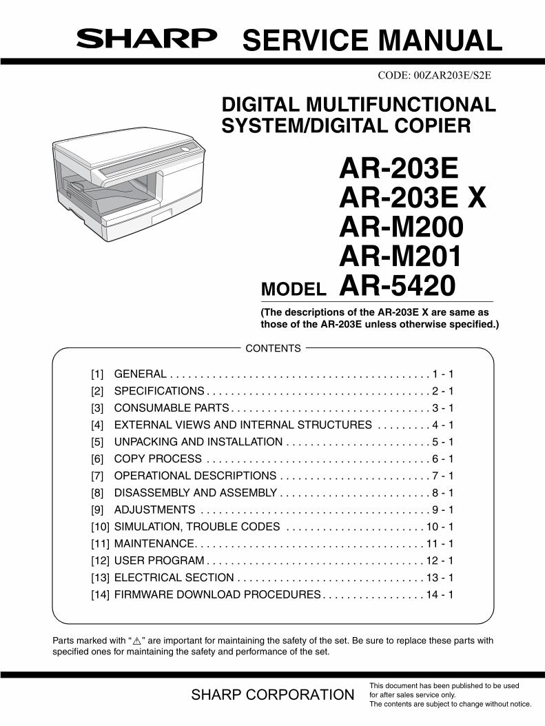
Parts marked with “ ” are important for maintaining the safety of the set. Be sure to replace these parts with specified ones for maintaining the safety and performance of the set. This document has been published to be used for after sales service only. The contents are subject to change without notice. SERVICE MANUAL CONTENTS SHARP CORPORATION CODE: 00ZAR203E/S2E DIGITAL MULTIFUNCTIONAL SYSTEM/DIGITAL COPIER AR-203E AR-203E X AR-M200 AR-M201 MODEL AR-5420 (The descriptions of the AR-203E X are same as those of the AR-203E unless otherwise specified.) [1] GENERAL . . . . . . . . . . . . . . . . . . . . . . . . . . . . . . . . . . . . . . . . . . . 1 - 1 [2] SPECIFICATIONS . . . . . . . . . . . . . . . . . . . . . . . . . . . . . . . . . . . . . 2 - 1 [3] CONSUMABLE PARTS . . . . . . . . . . . . . . . . . . . . . . . . . . . . . . . . . 3 - 1 [4] EXTERNAL VIEWS AND INTERNAL STRUCTURES . . . . . . . . . 4 - 1 [5] UNPACKING AND INSTALLATION . . . . . . . . . . . . . . . . . . . . . . . . 5 - 1 [6] COPY PROCESS . . . . . . . . . . . . . . . . . . . . . . . . . . . . . . . . . . . . . 6 - 1 [7] OPERATIONAL DESCRIPTIONS . . . . . . . . . . . . . . . . . . . . . . . . . 7 - 1 [8] DISASSEMBLY AND ASSEMBLY . . . . . . . . . . . . . . . . . . . . . . . . . 8 - 1 [9] ADJUSTMENTS . . . . . . . . . . . . . . . . . . . . . . . . . . . . . . . . . . . . . . 9 - 1 [10] SIMULATION, TROUBLE CODES . . . . . . . . . . . . . . . . . . . . . . . 10 - 1 [11] MAINTENANCE. . . . . . . . . . . . . . . . . . . . . . . . . . . . . . . . . . . . . . 11 - 1 [12] USER PROGRAM . . . . . . . . . . . . . . . . . . . . . . . . . . . . . . . . . . . . 12 - 1 [13] ELECTRICAL SECTION . . . . . . . . . . . . . . . . . . . . . . . . . . . . . . . 13 - 1 [14] FIRMWARE DOWNLOAD PROCEDURES . . . . . . . . . . . . . . . . . 14 - 1
-
Upload
mahesh-kamath-n -
Category
Documents
-
view
681 -
download
44
description
sharp mfp AR M201 service manual
Transcript of AR M201 Service manual
SERVICE MANUAL
Parts marked with “ ” are important for maintaining the safety of the set. Be sure to replace these parts withspecified ones for maintaining the safety and performance of the set.
CONTENTS
CODE: 00ZAR203E/S2E
DIGITAL MULTIFUNCTIONAL SYSTEM/DIGITAL COPIER
AR-203EAR-203E XAR-M200AR-M201
MODEL AR-5420(The descriptions of the AR-203E X are same as those of the AR-203E unless otherwise specified.)
[1] GENERAL . . . . . . . . . . . . . . . . . . . . . . . . . . . . . . . . . . . . . . . . . . . 1 - 1
[2] SPECIFICATIONS . . . . . . . . . . . . . . . . . . . . . . . . . . . . . . . . . . . . . 2 - 1
[3] CONSUMABLE PARTS . . . . . . . . . . . . . . . . . . . . . . . . . . . . . . . . . 3 - 1
[4] EXTERNAL VIEWS AND INTERNAL STRUCTURES . . . . . . . . . 4 - 1
[5] UNPACKING AND INSTALLATION . . . . . . . . . . . . . . . . . . . . . . . . 5 - 1
[6] COPY PROCESS . . . . . . . . . . . . . . . . . . . . . . . . . . . . . . . . . . . . . 6 - 1
[7] OPERATIONAL DESCRIPTIONS . . . . . . . . . . . . . . . . . . . . . . . . . 7 - 1
[8] DISASSEMBLY AND ASSEMBLY . . . . . . . . . . . . . . . . . . . . . . . . . 8 - 1
[9] ADJUSTMENTS . . . . . . . . . . . . . . . . . . . . . . . . . . . . . . . . . . . . . . 9 - 1
[10] SIMULATION, TROUBLE CODES . . . . . . . . . . . . . . . . . . . . . . . 10 - 1
[11] MAINTENANCE. . . . . . . . . . . . . . . . . . . . . . . . . . . . . . . . . . . . . . 11 - 1
[12] USER PROGRAM . . . . . . . . . . . . . . . . . . . . . . . . . . . . . . . . . . . . 12 - 1
[13] ELECTRICAL SECTION . . . . . . . . . . . . . . . . . . . . . . . . . . . . . . . 13 - 1
[14] FIRMWARE DOWNLOAD PROCEDURES . . . . . . . . . . . . . . . . . 14 - 1
This document has been published to be usedfor after sales service only.The contents are subject to change without notice.
SHARP CORPORATION
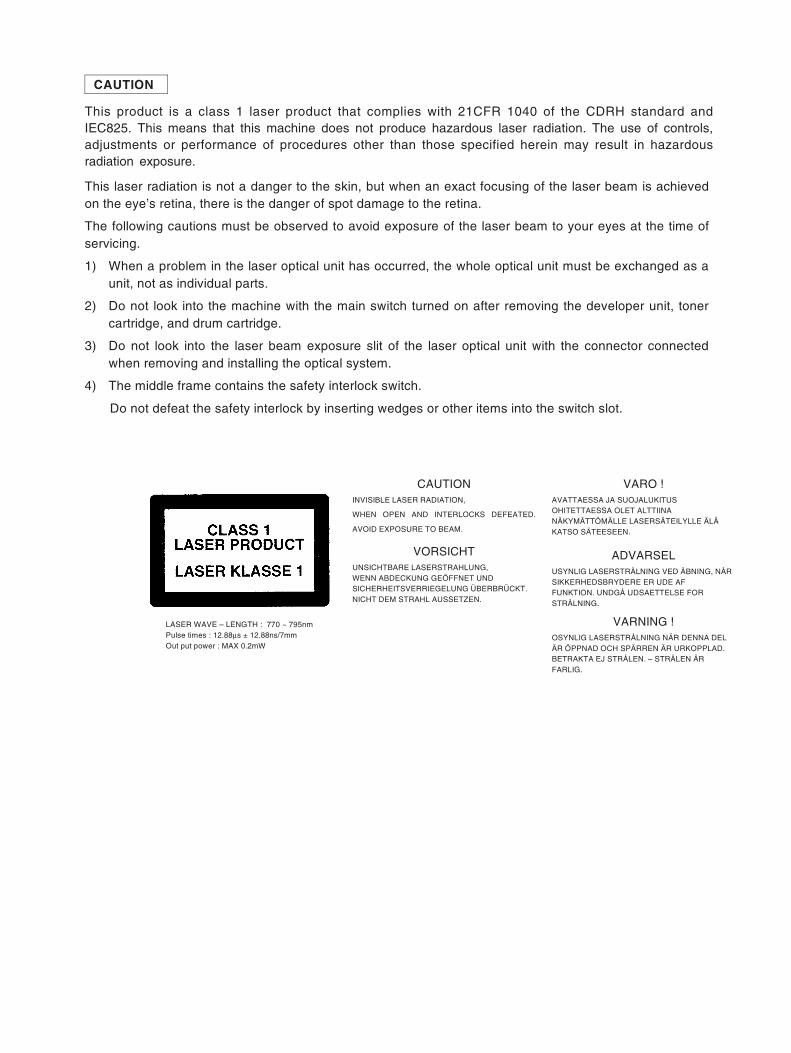
CAUTION
This laser radiation is not a danger to the skin, but when an exact focusing of the laser beam is achievedon the eye’s retina, there is the danger of spot damage to the retina.
The following cautions must be observed to avoid exposure of the laser beam to your eyes at the time ofservicing.
1) When a problem in the laser optical unit has occurred, the whole optical unit must be exchanged as aunit, not as individual parts.
2) Do not look into the machine with the main switch turned on after removing the developer unit, tonercartridge, and drum cartridge.
3) Do not look into the laser beam exposure slit of the laser optical unit with the connector connectedwhen removing and installing the optical system.
4) The middle frame contains the safety interlock switch.
Do not defeat the safety interlock by inserting wedges or other items into the switch slot.
LASER WAVE – LENGTH : 770 ~ 795nmPulse times : 12.88µs ± 12.88ns/7mmOut put power : MAX 0.2mW
CAUTIONINVISIBLE LASER RADIATION,
WHEN OPEN AND INTERLOCKS DEFEATED.
AVOID EXPOSURE TO BEAM.
VORSICHTUNSICHTBARE LASERSTRAHLUNG,WENN ABDECKUNG GEÖFFNET UNDSICHERHEITSVERRIEGELUNG ÜBERBRÜCKT.NICHT DEM STRAHL AUSSETZEN.
VARO !AVATTAESSA JA SUOJALUKITUSOHITETTAESSA OLET ALTTIINANÄKYMÄTTÖMÄLLE LASERSÄTEILYLLE ÄLÄKATSO SÄTEESEEN.
ADVARSELUSYNLIG LASERSTRÅLNING VED ÅBNING, NÅRSIKKERHEDSBRYDERE ER UDE AFFUNKTION. UNDGÅ UDSAETTELSE FORSTRÅLNING.
VARNING !OSYNLIG LASERSTRÅLNING NÄR DENNA DELÄR ÖPPNAD OCH SPÄRREN ÄR URKOPPLAD.BETRAKTA EJ STRÅLEN. – STRÅLEN ÄRFARLIG.
This product is a class 1 laser product that complies with 21CFR 1040 of the CDRH standard andIEC825. This means that this machine does not produce hazardous laser radiation. The use of controls,adjustments or performance of procedures other than those specified herein may result in hazardousradiation exposure.

At the production line, the output powerof the scanner unit is adjusted to 0.18MILLI-WATT PLUS 20 PCTS and ismaintained constant by the operation ofthe Automatic Power Control (APC).Even if the APC circuit fails in operationfor some reason, the maximum outputpower will only be 15 MILLI-WATT 0.1MICRO-SEC. Giving and accessibleemission level of 42 MICRO-WATTwhich is still-less than the limit ofCLASS-1 laser product.
The foregoing is applicable only to the 220Vmodel, 230V model and 240V model.
VAROITUS! LAITTEEN KÄYTTÄMINEN MUULLAKUIN TÄSSÄ KÄYTTÖOHJEESSA MAINITULLATAVALLA SAATTAA ALTISTAA KÄYTTÄJÄNTURVALLISUUSLUOKAN 1 YLITTÄVÄLLENÄKYMÄTTÖMÄLLE LASERSÄTEILYLLE.
VARNING - OM APPARATEN ANVÄNDS PÅ ANNATSÄTT ÄN I DENNA BRUKSANVISNINGSPECIFICERATS, KAN ANVÄNDAREN UTSÄTTASFÖR OSYNLIG LASERSTRÅLNING, SOMÖVERSKRIDER GRÄNSEN FÖR LASERKLASS 1.
CautionThis product contains a low power laserdevice. To ensure continued safety do notremove any cover or attempt to gain accessto the inside of the product. Refer allservicing to qualified personnel.
LUOKAN 1 LASERLAITEKLASS 1 LASER APPARAT

CONTENTS
[1] GENERAL
1. Major functions . . . . . . . . . . . . . . . . . . . . . . . . . . . . . . . 1-1
[2] SPECIFICATIONS
1. Basic Specifications . . . . . . . . . . . . . . . . . . . . . . . . . . . 2-1
2. Operation specifications . . . . . . . . . . . . . . . . . . . . . . . . 2-1
3. Copy performance . . . . . . . . . . . . . . . . . . . . . . . . . . . . 2-2
4. GDI printer (AR-203E only). . . . . . . . . . . . . . . . . . . . . . 2-3
5. SPLC printer (AR-M200/M201). . . . . . . . . . . . . . . . . . . 2-3
6. Scan function (AR-203E/M200/M201) . . . . . . . . . . . . . 2-3
[3] CONSUMABLE PARTS
1. Supply system table . . . . . . . . . . . . . . . . . . . . . . . . . . . 3-1
A. Europe Subsidiary (AR-203E/5420/M200/M201), SCA/SCNZ (AR-203E/M201) . . . . . . . . . . . . . . . . . . 3-1
B. Asia Subsidiary (AR-203E/M201). . . . . . . . . . . . . . . 3-1
C. SMEF/Distributor (AR-203E/M201) . . . . . . . . . . . . . 3-1
D. SRH (AR-203E/M201) . . . . . . . . . . . . . . . . . . . . . . . 3-1
2. Environmental . . . . . . . . . . . . . . . . . . . . . . . . . . . . . . . . 3-2
3. Production control number (lot No.) identification . . . . . 3-2
4. Toner cartridge replacement. . . . . . . . . . . . . . . . . . . . . 3-3
[4] EXTERNAL VIEWS AND INTERNAL STRUCTURES
1. Appearance . . . . . . . . . . . . . . . . . . . . . . . . . . . . . . . . . 4-1
2. Internal . . . . . . . . . . . . . . . . . . . . . . . . . . . . . . . . . . . . . 4-1
3. Operation panel . . . . . . . . . . . . . . . . . . . . . . . . . . . . . . 4-2
A. AR-203E/5420 . . . . . . . . . . . . . . . . . . . . . . . . . . . . . 4-2
B. AR-M200/M201 . . . . . . . . . . . . . . . . . . . . . . . . . . . . 4-3
4. Motors and solenoids . . . . . . . . . . . . . . . . . . . . . . . . . . 4-5
5. Sensors and switches . . . . . . . . . . . . . . . . . . . . . . . . . . 4-6
6. PWB unit . . . . . . . . . . . . . . . . . . . . . . . . . . . . . . . . . . . . 4-7
7. Cross sectional view . . . . . . . . . . . . . . . . . . . . . . . . . . . 4-8
[5] UNPACKING AND INSTALLATION
1. Copier installation . . . . . . . . . . . . . . . . . . . . . . . . . . . . . 5-1
2. Cautions on handling . . . . . . . . . . . . . . . . . . . . . . . . . . 5-1
3. Checking packed components and accessories. . . . . . 5-1
4. Unpacking. . . . . . . . . . . . . . . . . . . . . . . . . . . . . . . . . . . 5-2
5. Removing protective packing materials . . . . . . . . . . . . 5-2
6. Developer unit installation. . . . . . . . . . . . . . . . . . . . . . . 5-2
7. Toner cartridge installation . . . . . . . . . . . . . . . . . . . . . . 5-3
8. Loading paper. . . . . . . . . . . . . . . . . . . . . . . . . . . . . . . . 5-4
9. Power to copier . . . . . . . . . . . . . . . . . . . . . . . . . . . . . . . 5-4
10. Software (AR-203E/M200/M201) . . . . . . . . . . . . . . . . . 5-4
A. Before installation. . . . . . . . . . . . . . . . . . . . . . . . . . . 5-4
B. Installing the software. . . . . . . . . . . . . . . . . . . . . . . . 5-5
C. Setting up Button Manager. . . . . . . . . . . . . . . . . . . . 5-7
11. Interface . . . . . . . . . . . . . . . . . . . . . . . . . . . . . . . . . . . . 5-9
A. USB . . . . . . . . . . . . . . . . . . . . . . . . . . . . . . . . . . . . . 5-9
12. Moving . . . . . . . . . . . . . . . . . . . . . . . . . . . . . . . . . . . . . 5-9
13. Scanner moisture-proof kit . . . . . . . . . . . . . . . . . . . . . . 5-9
A. Components . . . . . . . . . . . . . . . . . . . . . . . . . . . . . . . 5-9
B. Precautions at installation . . . . . . . . . . . . . . . . . . . . 5-9
C. Attachment method . . . . . . . . . . . . . . . . . . . . . . . . . 5-9
[6] COPY PROCESS
1. Functional diagram . . . . . . . . . . . . . . . . . . . . . . . . . . . . 6-1
2. Outline of print process . . . . . . . . . . . . . . . . . . . . . . . . . 6-2
3. Actual print process . . . . . . . . . . . . . . . . . . . . . . . . . . . 6-2
[7] OPERATIONAL DESCRIPTIONS
1. Outline of operation. . . . . . . . . . . . . . . . . . . . . . . . . . . . 7-1
2. Scanner section . . . . . . . . . . . . . . . . . . . . . . . . . . . . . . 7-2
A. Scanner unit . . . . . . . . . . . . . . . . . . . . . . . . . . . . . . . 7-2
B. Optical system . . . . . . . . . . . . . . . . . . . . . . . . . . . . . 7-2
C. Drive system. . . . . . . . . . . . . . . . . . . . . . . . . . . . . . . 7-2
3. Laser unit . . . . . . . . . . . . . . . . . . . . . . . . . . . . . . . . . . .7-3
A. Basic structure . . . . . . . . . . . . . . . . . . . . . . . . . . . . . 7-3
B. Laser beam path. . . . . . . . . . . . . . . . . . . . . . . . . . . . 7-3
C. Composition . . . . . . . . . . . . . . . . . . . . . . . . . . . . . . . 7-3
4. Fuser section . . . . . . . . . . . . . . . . . . . . . . . . . . . . . . . . 7-3
A. General description . . . . . . . . . . . . . . . . . . . . . . . . . 7-4
5. Paper feed section and paper transport section . . . . . . 7-4
A. Paper transport path and general operations . . . . . . 7-4
6. D-D (Duplex to Duplex) mode paper/document transport (Duplex model) (AR-M201 only) . . . . . . . . . . . . . . . . . . . . . . . . . . . . . . . 7-7
A. Initial state . . . . . . . . . . . . . . . . . . . . . . . . . . . . . . . . 7-7
B. Front copy. . . . . . . . . . . . . . . . . . . . . . . . . . . . . . . . . 7-7
C. Back copy . . . . . . . . . . . . . . . . . . . . . . . . . . . . . . . . . 7-7
7. Shifter (AR-M200/M201) . . . . . . . . . . . . . . . . . . . . . . . .7-8
[8] DISASSEMBLY AND ASSEMBLY
1. High voltage section . . . . . . . . . . . . . . . . . . . . . . . . . . . 8-1
A. List . . . . . . . . . . . . . . . . . . . . . . . . . . . . . . . . . . . . . . 8-1
B. Drum replacement . . . . . . . . . . . . . . . . . . . . . . . . . . 8-1
C. Disassembly procedure . . . . . . . . . . . . . . . . . . . . . . 8-3
D. Assembly procedure. . . . . . . . . . . . . . . . . . . . . . . . .8-3
E. Charger wire cleaning. . . . . . . . . . . . . . . . . . . . . . . .8-4
F. Charger wire replacement . . . . . . . . . . . . . . . . . . . . 8-4
2. Operation panel section . . . . . . . . . . . . . . . . . . . . . . . . 8-4
A. List . . . . . . . . . . . . . . . . . . . . . . . . . . . . . . . . . . . . . . 8-4
B. Disassembly procedure . . . . . . . . . . . . . . . . . . . . . . 8-4
C. Assembly procedure. . . . . . . . . . . . . . . . . . . . . . . . .8-5
3. Optical section . . . . . . . . . . . . . . . . . . . . . . . . . . . . . . . 8-5
A. List . . . . . . . . . . . . . . . . . . . . . . . . . . . . . . . . . . . . . . 8-5
B. Disassembly procedure . . . . . . . . . . . . . . . . . . . . . . 8-5
C. Assembly procedure. . . . . . . . . . . . . . . . . . . . . . . . .8-7
4. Fusing section. . . . . . . . . . . . . . . . . . . . . . . . . . . . . . . . 8-7
A. List . . . . . . . . . . . . . . . . . . . . . . . . . . . . . . . . . . . . . . 8-7
B. Disassembly procedure . . . . . . . . . . . . . . . . . . . . . . 8-7
C. Assembly procedure. . . . . . . . . . . . . . . . . . . . . . . .8-10
5. Tray paper feed/transport section . . . . . . . . . . . . . . . . 8-10
A. List . . . . . . . . . . . . . . . . . . . . . . . . . . . . . . . . . . . . . 8-10
B. Disassembly procedure . . . . . . . . . . . . . . . . . . . . . 8-10
C. Assembly procedure. . . . . . . . . . . . . . . . . . . . . . . .8-16
6. Manual paper feed section . . . . . . . . . . . . . . . . . . . . . 8-16
A. List . . . . . . . . . . . . . . . . . . . . . . . . . . . . . . . . . . . . . 8-16
B. Disassembly procedure . . . . . . . . . . . . . . . . . . . . . 8-16
C. Assembly procedure. . . . . . . . . . . . . . . . . . . . . . . .8-18
D. Pressure plate holder attachment. . . . . . . . . . . . . . 8-18
7. Rear frame section . . . . . . . . . . . . . . . . . . . . . . . . . . . 8-18
A. List . . . . . . . . . . . . . . . . . . . . . . . . . . . . . . . . . . . . . 8-18
B. Disassembly procedure . . . . . . . . . . . . . . . . . . . . . 8-18
C. Assembly procedure. . . . . . . . . . . . . . . . . . . . . . . .8-19
8 Power section . . . . . . . . . . . . . . . . . . . . . . . . . . . . . . . 8-20
A. List . . . . . . . . . . . . . . . . . . . . . . . . . . . . . . . . . . . . . 8-20
B. Disassembly procedure . . . . . . . . . . . . . . . . . . . . . 8-20
C. Assembly procedure. . . . . . . . . . . . . . . . . . . . . . . . 8-20
9. DV unit section . . . . . . . . . . . . . . . . . . . . . . . . . . . . . . 8-20
A. Developer . . . . . . . . . . . . . . . . . . . . . . . . . . . . . . . . 8-20
B. DV seal. . . . . . . . . . . . . . . . . . . . . . . . . . . . . . . . . . 8-20
C. DV blade. . . . . . . . . . . . . . . . . . . . . . . . . . . . . . . . . 8-21
D. DV doctor . . . . . . . . . . . . . . . . . . . . . . . . . . . . . . . . 8-21
E. DV sensor. . . . . . . . . . . . . . . . . . . . . . . . . . . . . . . . 8-21
10. Duplex motor section (AR-M201 only) . . . . . . . . . . . . 8-21
A. List . . . . . . . . . . . . . . . . . . . . . . . . . . . . . . . . . . . . . 8-21
B. Disassembly procedure . . . . . . . . . . . . . . . . . . . . . 8-21
C. Assembly procedure. . . . . . . . . . . . . . . . . . . . . . . . 8-21
11. Reverse roller section (AR-M201 only). . . . . . . . . . . . 8-22
A. List . . . . . . . . . . . . . . . . . . . . . . . . . . . . . . . . . . . . . 8-22
B. Disassembly procedure . . . . . . . . . . . . . . . . . . . . . 8-22
C. Assembly procedure. . . . . . . . . . . . . . . . . . . . . . . . 8-22
[9] ADJUSTMENTS
1. Optical section . . . . . . . . . . . . . . . . . . . . . . . . . . . . . . . 9-1
A. Copy magnification ratio adjustment . . . . . . . . . . . . 9-1
B. Image position adjustment . . . . . . . . . . . . . . . . . . . . 9-2
2. Copy density adjustment . . . . . . . . . . . . . . . . . . . . . . . 9-4
A. Copy density adjustment timing . . . . . . . . . . . . . . . . 9-4
B. Note for copy density adjustment . . . . . . . . . . . . . . . 9-4
C. Necessary tool for copy density adjustment. . . . . . . 9-4
D. Features of copy density adjustment . . . . . . . . . . . . 9-4
E. Copy density adjustment procedure. . . . . . . . . . . . . 9-5
3. High voltage adjustment . . . . . . . . . . . . . . . . . . . . . . . . 9-5
A. Main charger (Grid bias). . . . . . . . . . . . . . . . . . . . . . 9-5
B. DV bias check . . . . . . . . . . . . . . . . . . . . . . . . . . . . . 9-6
4. Duplex adjustment . . . . . . . . . . . . . . . . . . . . . . . . . . . . 9-6
A. Adjusting the paper reverse position in memory for duplex copying (AR-M200/M201) . . . . . . . . . . . . 9-6
B. Adjusting trailing edge void in duplex copy mode (AR-M201) . . . . . . . . . . . . . . . . . . . . . . . . . . . . . . . . 9-6
5. Automatic black level correction . . . . . . . . . . . . . . . . . . 9-7
[10] SIMULATION, TROUBLE CODES
1. Entering the simulation mode . . . . . . . . . . . . . . . . . . . 10-1
2. Key rule. . . . . . . . . . . . . . . . . . . . . . . . . . . . . . . . . . . . 10-1
3. List of simulations . . . . . . . . . . . . . . . . . . . . . . . . . . . . 10-1
4. Descriptions of various simulations. . . . . . . . . . . . . . . 10-3
5. Trouble codes . . . . . . . . . . . . . . . . . . . . . . . . . . . . . . 10-40
A. Trouble codes list . . . . . . . . . . . . . . . . . . . . . . . . . 10-40
B. Details of trouble codes . . . . . . . . . . . . . . . . . . . . 10-41
[11] MAINTENANCE
1. Maintenance table . . . . . . . . . . . . . . . . . . . . . . . . . . . 11-1
2. Maintenance display system. . . . . . . . . . . . . . . . . . . . 11-1
3. Remaining toner indication . . . . . . . . . . . . . . . . . . . . . 11-1
[12] USER PROGRAM
1. Functions that can be set with user programs . . . . . . 12-1
2. Toner save mode (AR-203E/5420) . . . . . . . . . . . . . . . 12-1
3. User programs (AR-203E/5420) . . . . . . . . . . . . . . . . . 12-1
4. User programs (AR-M200/M201) . . . . . . . . . . . . . . . . 12-2
A. Copy mode . . . . . . . . . . . . . . . . . . . . . . . . . . . . . . . 12-3
B. Print mode . . . . . . . . . . . . . . . . . . . . . . . . . . . . . . . 12-4
[13] ELECTRICAL SECTION
1. Block diagram . . . . . . . . . . . . . . . . . . . . . . . . . . . . . . . 13-1
A. Overall block diagram (AR-203E/5420) . . . . . . . . . 13-1
B. Overall block diagram (AR-M200/M201) . . . . . . . . 13-2
2. Actual wiring diagram . . . . . . . . . . . . . . . . . . . . . . . . . 13-3
A. MCU PWB (AR-203E/5420) . . . . . . . . . . . . . . . . . . 13-3
B. MCU PWB (AR-M200/M201) . . . . . . . . . . . . . . . . . 13-4
C. SPF unit (AR-203E optional only). . . . . . . . . . . . . . 13-5
D. RSPF unit (AR-M200/M201 optional only) . . . . . . . 13-5
E. 2nd cassette unit (AR-203E/M200/M201 optional only) . . . . . . . . . . . 13-5
F. Network box and FAX (AR-M200/M201 optional only). . . . . . . . . . . . . . . . 13-6
3. Signal name list. . . . . . . . . . . . . . . . . . . . . . . . . . . . . . 13-6
4. Circuit diagram . . . . . . . . . . . . . . . . . . . . . . . . . . . . . . 13-9
A. MCU PWB (AR-203E/5420) . . . . . . . . . . . . . . . . . . 13-9
B. MCU PWB (AR-M200/M201) . . . . . . . . . . . . . . . . 13-21
C. OPE PWB (AR-203E/5420) . . . . . . . . . . . . . . . . . 13-37
D. OPERATION PWB (AR-M200/M201). . . . . . . . . . 13-38
[14] FIRMWARE DOWNLOAD PROCEDURES
1. Initial setting (Serial number setting procedures) . . . . 14-1
2. Download procedures . . . . . . . . . . . . . . . . . . . . . . . . .14-1
3. Version acquisition procedures . . . . . . . . . . . . . . . . . . 14-3
4. EEPROM data acquisition procedure . . . . . . . . . . . . . 14-4
5. Installing procedures. . . . . . . . . . . . . . . . . . . . . . . . . . 14-5
AR-203E/5420/M200/M201 GENERAL 1 - 1
[1] GENERAL
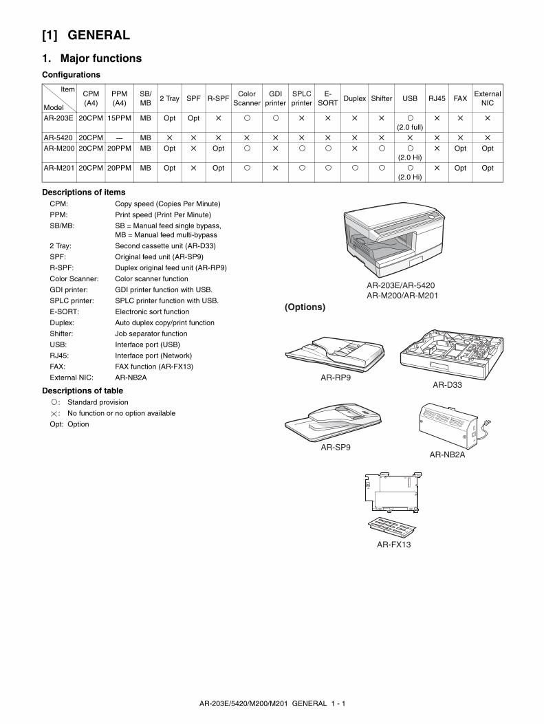
1. Major functionsConfigurations
Descriptions of itemsCPM: Copy speed (Copies Per Minute)
PPM: Print speed (Print Per Minute)
SB/MB: SB = Manual feed single bypass, MB = Manual feed multi-bypass
2 Tray: Second cassette unit (AR-D33)
SPF: Original feed unit (AR-SP9)
R-SPF: Duplex original feed unit (AR-RP9)
Color Scanner: Color scanner function
GDI printer: GDI printer function with USB.
SPLC printer: SPLC printer function with USB.
E-SORT: Electronic sort function
Duplex: Auto duplex copy/print function
Shifter: Job separator function
USB: Interface port (USB)
RJ45: Interface port (Network)
FAX: FAX function (AR-FX13)
External NIC: AR-NB2A
Descriptions of table: Standard provision
: No function or no option available
Opt: Option
Item
Model
CPM (A4)
PPM (A4)
SB/MB
2 Tray SPF R-SPFColor
ScannerGDI
printerSPLC printer
E-SORT
Duplex Shifter USB RJ45 FAXExternal
NIC
AR-203E 20CPM 15PPM MB Opt Opt
(2.0 full)
AR-5420 20CPM — MB
AR-M200 20CPM 20PPM MB Opt Opt
(2.0 Hi) Opt Opt
AR-M201 20CPM 20PPM MB Opt Opt
(2.0 Hi) Opt Opt
AR-SP9
(Options)
AR-D33
AR-203E/AR-5420AR-M200/AR-M201
AR-NB2A
AR-FX13
AR-RP9
[2] SPECIFICATIONS
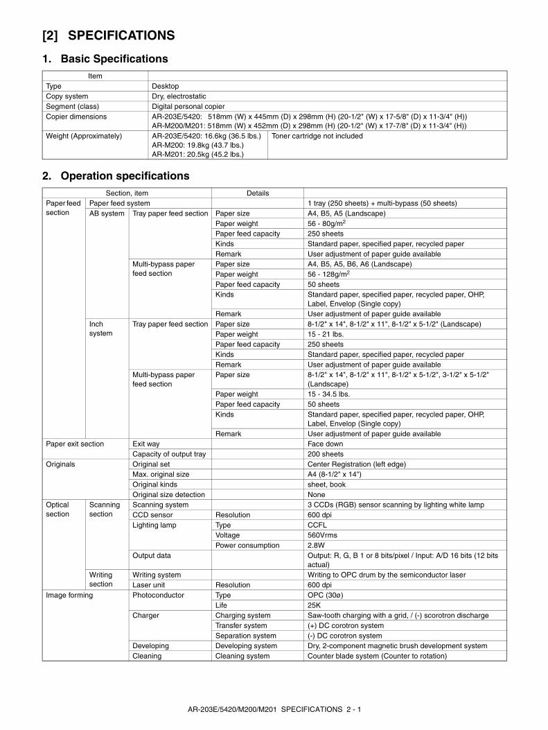
1. Basic Specifications
2. Operation specifications
ItemType DesktopCopy system Dry, electrostaticSegment (class) Digital personal copierCopier dimensions AR-203E/5420: 518mm (W) x 445mm (D) x 298mm (H) (20-1/2" (W) x 17-5/8" (D) x 11-3/4" (H))
AR-M200/M201: 518mm (W) x 452mm (D) x 298mm (H) (20-1/2" (W) x 17-7/8" (D) x 11-3/4" (H))Weight (Approximately) AR-203E/5420: 16.6kg (36.5 lbs.)
AR-M200: 19.8kg (43.7 lbs.)AR-M201: 20.5kg (45.2 lbs.)
Toner cartridge not included
Section, item DetailsPaper feed section
Paper feed system 1 tray (250 sheets) + multi-bypass (50 sheets)AB system Tray paper feed section Paper size A4, B5, A5 (Landscape)
Paper weight 56 - 80g/m2
Paper feed capacity 250 sheetsKinds Standard paper, specified paper, recycled paperRemark User adjustment of paper guide available
Multi-bypass paper feed section
Paper size A4, B5, A5, B6, A6 (Landscape)Paper weight 56 - 128g/m2
Paper feed capacity 50 sheetsKinds Standard paper, specified paper, recycled paper, OHP,
Label, Envelop (Single copy)Remark User adjustment of paper guide available
Inch system
Tray paper feed section Paper size 8-1/2" x 14", 8-1/2" x 11", 8-1/2" x 5-1/2" (Landscape)Paper weight 15 - 21 lbs.Paper feed capacity 250 sheetsKinds Standard paper, specified paper, recycled paperRemark User adjustment of paper guide available
Multi-bypass paper feed section
Paper size 8-1/2" x 14", 8-1/2" x 11", 8-1/2" x 5-1/2", 3-1/2" x 5-1/2" (Landscape)
Paper weight 15 - 34.5 lbs.Paper feed capacity 50 sheetsKinds Standard paper, specified paper, recycled paper, OHP,
Label, Envelop (Single copy)Remark User adjustment of paper guide available
Paper exit section Exit way Face downCapacity of output tray 200 sheets
Originals Original set Center Registration (left edge)Max. original size A4 (8-1/2" x 14")Original kinds sheet, bookOriginal size detection None
Optical section
Scanning section
Scanning system 3 CCDs (RGB) sensor scanning by lighting white lampCCD sensor Resolution 600 dpiLighting lamp Type CCFL
Voltage 560VrmsPower consumption 2.8W
Output data Output: R, G, B 1 or 8 bits/pixel / Input: A/D 16 bits (12 bits actual)
Writing section
Writing system Writing to OPC drum by the semiconductor laserLaser unit Resolution 600 dpi
Image forming Photoconductor Type OPC (30ø)Life 25K
Charger Charging system Saw-tooth charging with a grid, / (-) scorotron dischargeTransfer system (+) DC corotron systemSeparation system (-) DC corotron system
Developing Developing system Dry, 2-component magnetic brush development systemCleaning Cleaning system Counter blade system (Counter to rotation)
AR-203E/5420/M200/M201 SPECIFICATIONS 2 - 1

3. Copy performance
*1: If a value greater than 200% or smaller than 50% is selected when the RSPF is used, the magnification ratio is automatically set to 200% or50%.
*2: The first-copy time is measured after the power save indicator turns off following power on, using the document glass with the polygon rotat-ing in the copy ready state and "Selection of copy start state" set to ON in the user programs (A4 (8-1/2" x 11"), paper fed from paper tray).
The first-copy time may vary depending on machine operating conditions and ambient conditions such as temperature.
Fusing section Fusing system Heat roller systemUpper heat roller Type Teflon rollerLower heat roller Type Silicon rubber rollerHeater lamp Type Halogen lamp
Voltage 220 - 240V / 120VPower consumption 800W
Electrical section Power source Voltage 220 - 240V / 120VFrequency Common use for 50 and 60Hz
Power consumption Max. Less than 1000WAverage (during copying) AR-203E/5420: 350Wh/H or less
AR-M200/ M201: 380Wh/H or lessAverage (stand-by) 80Wh/HPre-heat mode AR-203E/5420: 25Wh/H or less
AR-M200/ M201: 28Wh/H or lessAuto power shut-off mode AR-203E/5420: 8.8W or less
AR-M200/ M201: 12.5W or less
Section, item DetailsCopy magnification Fixed
magnification ratios
AR-203E/5420:3 Reduction + 2 Enlargement(AB system: 50, 70, 86, 100, 141, 200%)(Inch system: 50, 64, 78, 100, 129, 200%)
AR-M200/M201: *14 Reduction + 3 Enlargement(AB system: 25, 50, 70, 86, 100, 141, 200, 400%)(Inch system: 25, 50, 64, 78, 100, 129, 200, 400%)
Zooming magnification ratios
25 - 400% (376 steps in 1% increments)50 - 200% when using SPF (151 steps in 1% increments)
Manual steps (manual, photo) 5 stepsCopy speed First-copy time *2
(Approximately)AR-203E/5420:
8.0 seconds (When user program 24 is set to OFF)10.7 seconds (When user program 24 is set to ON)
AR-M200/M201:8.0 seconds
(paper: A4 (8-1/2" x 11"), exposure mode: AUTO, copy ratio: 100%)AB systemA4 (Landscape)
Copy speed (CPM)
Same size 20Enlargement 20Reduction 20
AB systemB5 (Landscape)
Copy speed (CPM)
Same size 20Enlargement 20Reduction 20
Inch system8-1/2" x 11" (Landscape)
Copy speed (CPM)
Same size 20Enlargement 20Reduction 20
Max. continuous copy quantity 99Void Void area Leading edge 1 - 4mm
Trailing edge 4mm or lessSide edge void area
0.5mm or more (per side)4.5mm or less (total of both sides)
Image loss Leading edge same size: 3.0mm or less (OC) / 4mm or less (SPF)Enlarge: 1.5mm or less (OC) / 3mm or less (SPF)Reduction (50%): 6.0mm or less (OC) / 8mm or less (SPF)
Warm-up time 0 sec. Immediately the ready lamp is lit.Power save mode reset time 0 sec. Immediately the ready lamp is lit.Paper jam recovery time 0 sec.
∗ Jam recovery condition: Recovery time from 60 sec of door open.
Section, item Details
AR-203E/5420/M200/M201 SPECIFICATIONS 2 - 2
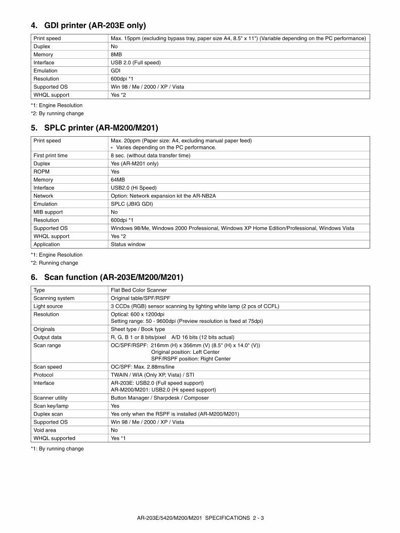
4. GDI printer (AR-203E only)
*1: Engine Resolution
*2: By running change
5. SPLC printer (AR-M200/M201)
*1: Engine Resolution
*2: Running change
6. Scan function (AR-203E/M200/M201)
*1: By running change
Print speed Max. 15ppm (excluding bypass tray, paper size A4, 8.5" x 11") (Variable depending on the PC performance)
Duplex No
Memory 8MB
Interface USB 2.0 (Full speed)
Emulation GDI
Resolution 600dpi *1
Supported OS Win 98 / Me / 2000 / XP / Vista
WHQL support Yes *2
Print speed Max. 20ppm (Paper size: A4, excluding manual paper feed)∗ Varies depending on the PC performance.
First print time 8 sec. (without data transfer time)
Duplex Yes (AR-M201 only)
ROPM Yes
Memory 64MB
Interface USB2.0 (Hi Speed)
Network Option: Network expansion kit the AR-NB2A
Emulation SPLC (JBIG GDI)
MIB support No
Resolution 600dpi *1
Supported OS Windows 98/Me, Windows 2000 Professional, Windows XP Home Edition/Professional, Windows Vista
WHQL support Yes *2
Application Status window
Type Flat Bed Color Scanner
Scanning system Original table/SPF/RSPF
Light source 3 CCDs (RGB) sensor scanning by lighting white lamp (2 pcs of CCFL)
Resolution Optical: 600 x 1200dpiSetting range: 50 - 9600dpi (Preview resolution is fixed at 75dpi)
Originals Sheet type / Book type
Output data R, G, B 1 or 8 bits/pixel A/D 16 bits (12 bits actual)
Scan range OC/SPF/RSPF: 216mm (H) x 356mm (V) (8.5" (H) x 14.0" (V))Original position: Left CenterSPF/RSPF position: Right Center
Scan speed OC/SPF: Max. 2.88ms/line
Protocol TWAIN / WIA (Only XP, Vista) / STI
Interface AR-203E: USB2.0 (Full speed support)AR-M200/M201: USB2.0 (Hi speed support)
Scanner utility Button Manager / Sharpdesk / Composer
Scan key/lamp Yes
Duplex scan Yes only when the RSPF is installed (AR-M200/M201)
Supported OS Win 98 / Me / 2000 / XP / Vista
Void area No
WHQL supported Yes *1
AR-203E/5420/M200/M201 SPECIFICATIONS 2 - 3
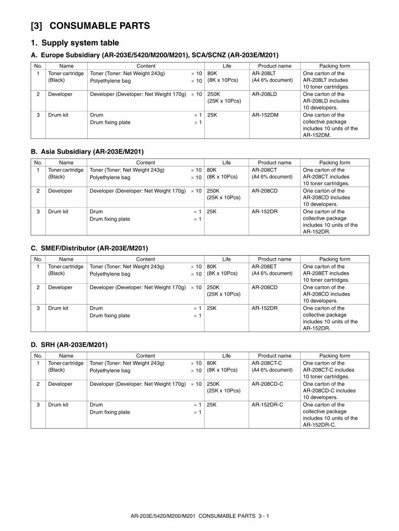
[3] CONSUMABLE PARTS
1. Supply system tableA. Europe Subsidiary (AR-203E/5420/M200/M201), SCA/SCNZ (AR-203E/M201)
B. Asia Subsidiary (AR-203E/M201)
C. SMEF/Distributor (AR-203E/M201)
D. SRH (AR-203E/M201)
No. Name Content Life Product name Packing form1 Toner cartridge
(Black)Toner (Toner: Net Weight 243g) × 10 80K
(8K x 10Pcs)AR-208LT(A4 6% document)
One carton of the AR-208LT includes 10 toner cartridges.
Polyethylene bag × 10
2 Developer Developer (Developer: Net Weight 170g) × 10 250K(25K x 10Pcs)
AR-208LD One carton of the AR-208LD includes 10 developers.
3 Drum kit Drum × 1 25K AR-152DM One carton of the collective package includes 10 units of the AR-152DM.
Drum fixing plate × 1
No. Name Content Life Product name Packing form1 Toner cartridge
(Black)Toner (Toner: Net Weight 243g) × 10 80K
(8K x 10Pcs)AR-208CT(A4 6% document)
One carton of the AR-208CT includes 10 toner cartridges.
Polyethylene bag × 10
2 Developer Developer (Developer: Net Weight 170g) × 10 250K(25K x 10Pcs)
AR-208CD One carton of the AR-208CD includes 10 developers.
3 Drum kit Drum × 1 25K AR-152DR One carton of the collective package includes 10 units of the AR-152DR.
Drum fixing plate × 1
No. Name Content Life Product name Packing form1 Toner cartridge
(Black)Toner (Toner: Net Weight 243g) × 10 80K
(8K x 10Pcs)AR-208ET(A4 6% document)
One carton of the AR-208ET includes 10 toner cartridges.
Polyethylene bag × 10
2 Developer Developer (Developer: Net Weight 170g) × 10 250K(25K x 10Pcs)
AR-208CD One carton of the AR-208CD includes 10 developers.
3 Drum kit Drum × 1 25K AR-152DR One carton of the collective package includes 10 units of the AR-152DR.
Drum fixing plate × 1
No. Name Content Life Product name Packing form1 Toner cartridge
(Black)Toner (Toner: Net Weight 243g) × 10 80K
(8K x 10Pcs)AR-208CT-C(A4 6% document)
One carton of the AR-208CT-C includes 10 toner cartridges.
Polyethylene bag × 10
2 Developer Developer (Developer: Net Weight 170g) × 10 250K(25K x 10Pcs)
AR-208CD-C One carton of the AR-208CD-C includes 10 developers.
3 Drum kit Drum × 1 25K AR-152DR-C One carton of the collective package includes 10 units of the AR-152DR-C.
Drum fixing plate × 1
AR-203E/5420/M200/M201 CONSUMABLE PARTS 3 - 1

2. EnvironmentalThe environmental conditions for assuring the copy quality and themachine operations are as follows:
(1) Normal operating conditionTemperature: 20 - 25°C
Humidity: 65 ± 5%RH
(2) Acceptable operating condition
(3) Transport condition
(4) Supply storage condition
3. Production control number (lot No.) identification
<Toner cartridge>
<Drum cartridge>
The label on the drum cartridge shows the date of production.
(SOCC production)
*1: The production control label is not attached to the cartridge ofa China product.
Humidity (RH)
85%
60%
20%
10˚C 30˚C 35˚C
Humidity (RH)
90%
60%
15%
–25˚C 30˚C 40˚C
Humidity (RH)
90%
20%
–5˚C 45˚C
Production monthProduction dayDestination code (Dealer, distributor, OEM, etc.)Production place (SOCC: Fixed to B.)End digit of yearVersion No.
Production monthProduction dayDestination code (Dealer, distributor, OEM, etc.)Production place (SOCC: Fixed to B.)End digit of yearVersion No.
Production controllabel attachment position
Production controllabel attachment position(*1)
AR-203E/5420/M200/M201 CONSUMABLE PARTS 3 - 2

<Developer>
4. Toner cartridge replacement1) Open the front and side cabinets of the copier.
2) Keep holding Toner lever, and
3) Carefully pull out Toner unit from the copier.
4) Put Toner unit in a collection bag immediately after removing itfrom the copier
Note: Never carry exposed Toner unit. Be sure to put it in the col-lection bag.
Sub lotProduction dayProduction month End digit of yearProduction place
1
3
2
AR-203E/5420/M200/M201 CONSUMABLE PARTS 3 - 3
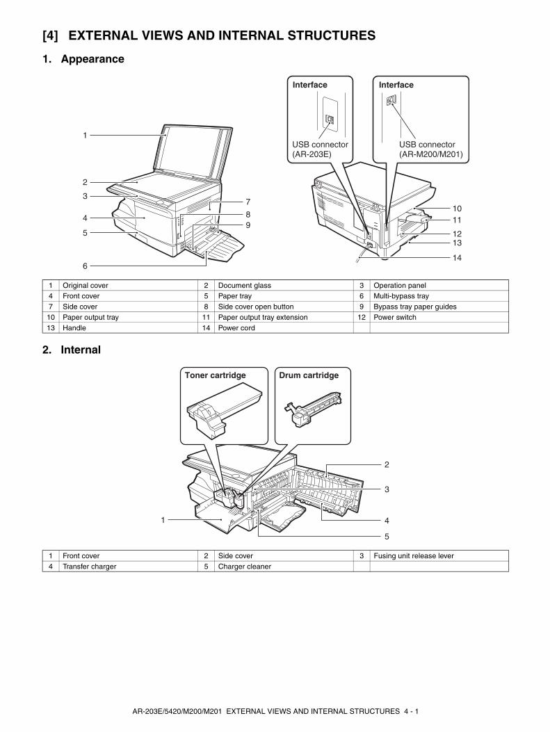
[4] EXTERNAL VIEWS AND INTERNAL STRUCTURES
1. Appearance
2. Internal
1 Original cover 2 Document glass 3 Operation panel4 Front cover 5 Paper tray 6 Multi-bypass tray
7 Side cover 8 Side cover open button 9 Bypass tray paper guides
10 Paper output tray 11 Paper output tray extension 12 Power switch
13 Handle 14 Power cord
1 Front cover 2 Side cover 3 Fusing unit release lever
4 Transfer charger 5 Charger cleaner
Interface
USB connector(AR-203E)
Interface
USB connector(AR-M200/M201)
3
4
5
1
2
7
98
6
1011
12
14
13
3
4
5
2
1
Toner cartridge Drum cartridge
AR-203E/5420/M200/M201 EXTERNAL VIEWS AND INTERNAL STRUCTURES 4 - 1
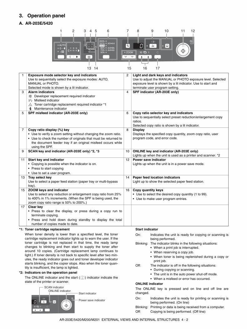
3. Operation panelA. AR-203E/5420
*1: Toner cartridge replacement
When toner density is lower than a specified level, the tonercartridge replacement indicator lights up to warn the user. If thetoner cartridge is not replaced in that time, the ready lampchanges to blinking and then start to supply the toner afteraround 10 copies. (Cartridge replacement lamp continues tolight.) If toner density is not back to specific level after two min-utes, the ready indicator goes out and toner developer indicatorstarts blinking, and the copier stops. Also when the toner quan-tity is insufficient, the lamp is lighted.
*2: Indicators on the operation panel
The ONLINE indicator and the start ( ) indicator indicate thestate of the printer or scanner.
Start indicator
ONLINE indicator
The ONLINE key is pressed and on line and off line arechanged.
1 Exposure mode selector key and indicatorsUse to sequentially select the exposure modes: AUTO, MANUAL or PHOTO.Selected mode is shown by a lit indicator.
2 Light and dark keys and indicatorsUse to adjust the MANUAL or PHOTO exposure level. Selected exposure level is shown by a lit indicator. Use to start and terminate user program setting.
3 Alarm indicatorsDeveloper replacement required indicatorMisfeed indicatorToner cartridge replacement required indicator *1Maintenance indicator
4 SPF indicator (AR-203E only)
5 SPF misfeed indicator (AR-203E only) 6 Copy ratio selector key and indicatorsUse to sequentially select preset reduction/enlargement copy ratios.Selected copy ratio is shown by a lit indicator.
7 Copy ratio display (%) key• Use to verify a zoom setting without changing the zoom ratio.• Use to check the number of originals that must be returned to
the document feeder tray if an original misfeed occurs whileusing the SPF.
8 DisplayDisplays the specified copy quantity, zoom copy ratio, user program code, and error code.
9 SCAN key and indicator (AR-203E only) *2, *3 10 ONLINE key and indicator (AR-203E only)Lights up when the unit is used as a printer and scanner. *2
11 Start key and indicator• Copying is possible when the indicator is on.• Press to start copying• Use to set a user program.
12 Power save indicatorLights up when the unit is in a power save mode.
13 Tray select keyUse to select a paper feed station (paper tray or multi-bypass tray).
14 Paper feed location indicatorsLight up to show the selected paper feed station.
15 ZOOM keys and indicatorUse to select any reduction or enlargement copy ratio from 25% to 400% in 1% increments. (When the SPF is being used, the zoom copy ratio range is 50% to 200%.)
16 Copy quantity keys• Use to select the desired copy quantity (1 to 99).• Use to make user program entries.
17 Clear key• Press to clear the display, or press during a copy run to
terminate copying.• Press and hold down during standby to display the total
number of copies made to date.
1 2 7 8 9 10 11 12
13 15 16 17
543
14
6
Power save indicator
Start indicatorONLINE indicator
SCAN indicator
On: Indicates the unit is ready for copying or scanning isbeing performed.
Blinking: The indicator blinks in the following situations:• When a print job is interrupted.• When reserving a copy job.• When toner is being replenished during a copy or
print job.Off: The indicator is off in the following situations:
• During copying or scanning.• The unit is in the auto power shut-off mode.• When a misfeed or error has occurred.
On: Indicates the unit is ready for printing or scanning isbeing performed. (On line)
Blinking: Printing or data is being received from a computer.Off: Copying is being performed. (Off line)
AR-203E/5420/M200/M201 EXTERNAL VIEWS AND INTERNAL STRUCTURES 4 - 2
Power save indicator
SCAN indicator
*3: Using the SCAN key to begin scanning
Note:
• Scanning is not possible during a copy job.
• If the SCAN ( ) key is pressed during a print job, the scanjob will be stored.
• When scanning an original that has been placed in the SPF,only one original can be placed unless you are using Sharp-desk.
1) Press the SCAN ( ) key.
The unit enters scan mode.
2) Place the original you wish to scan on the document glass/SPF.
3) Press the right copy quantity key to display the number ofthe application that you wish to use for scanning.
The application numbers are initially as follows.
4) Press the start ( ) key.
Scanning will start and the scanned data will be transferredto the application.
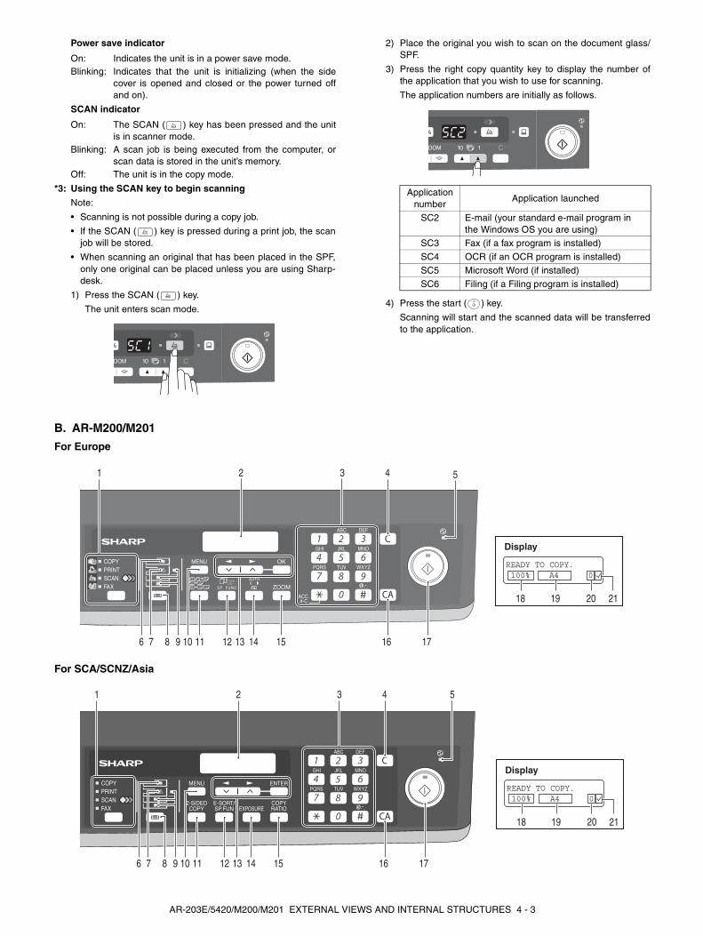
B. AR-M200/M201
For Europe
For SCA/SCNZ/Asia
On: Indicates the unit is in a power save mode.Blinking: Indicates that the unit is initializing (when the side
cover is opened and closed or the power turned offand on).
On: The SCAN ( ) key has been pressed and the unitis in scanner mode.
Blinking: A scan job is being executed from the computer, orscan data is stored in the unit’s memory.
Off: The unit is in the copy mode.
Application number
Application launched
SC2 E-mail (your standard e-mail program in the Windows OS you are using)
SC3 Fax (if a fax program is installed)
SC4 OCR (if an OCR program is installed)
SC5 Microsoft Word (if installed)
SC6 Filing (if a Filing program is installed)
6 7 8 10 11 12 14 159 16 17
1 1 22 22 1 1
13
READY TO COPY. 100% A4 0
Display
18 19 20 21
1 2 3 4 5
1 2
6 7 8 10 11 1312 14 159 16
3 4 5
17
READY TO COPY. 100% A4 0
Display
18 19 20 21
AR-203E/5420/M200/M201 EXTERNAL VIEWS AND INTERNAL STRUCTURES 4 - 3
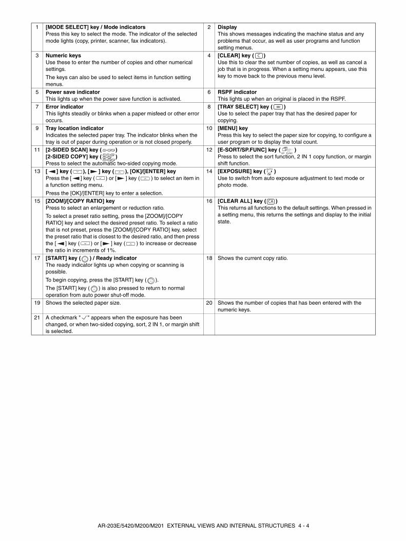
1 [MODE SELECT] key / Mode indicatorsPress this key to select the mode. The indicator of the selected mode lights (copy, printer, scanner, fax indicators).
2 DisplayThis shows messages indicating the machine status and any problems that occur, as well as user programs and function setting menus.
3 Numeric keysUse these to enter the number of copies and other numerical settings.
The keys can also be used to select items in function setting menus.
4 [CLEAR] key ( )Use this to clear the set number of copies, as well as cancel a job that is in progress. When a setting menu appears, use this key to move back to the previous menu level.
5 Power save indicatorThis lights up when the power save function is activated.
6 RSPF indicatorThis lights up when an original is placed in the RSPF.
7 Error indicatorThis lights steadily or blinks when a paper misfeed or other error occurs.
8 [TRAY SELECT] key ( )Use to select the paper tray that has the desired paper for copying.
9 Tray location indicatorIndicates the selected paper tray. The indicator blinks when the tray is out of paper during operation or is not closed properly.
10 [MENU] keyPress this key to select the paper size for copying, to configure a user program or to display the total count.
11 [2-SIDED SCAN] key ( )[2-SIDED COPY] key ( )Press to select the automatic two-sided copying mode.
12 [E-SORT/SP.FUNC] key ( )Press to select the sort function, 2 IN 1 copy function, or margin shift function.
13 [ ] key ( ), [ ] key ( ), [OK]/[ENTER] keyPress the [ ] key ( ) or [ ] key ( ) to select an item in a function setting menu.
Press the [OK]/[ENTER] key to enter a selection.
14 [EXPOSURE] key ( )Use to switch from auto exposure adjustment to text mode or photo mode.
15 [ZOOM]/[COPY RATIO] keyPress to select an enlargement or reduction ratio.
To select a preset ratio setting, press the [ZOOM]/[COPY RATIO] key and select the desired preset ratio. To select a ratio that is not preset, press the [ZOOM]/[COPY RATIO] key, select the preset ratio that is closest to the desired ratio, and then press the [ ] key ( ) or [ ] key ( ) to increase or decrease the ratio in increments of 1%.
16 [CLEAR ALL] key ( )This returns all functions to the default settings. When pressed in a setting menu, this returns the settings and display to the initial state.
17 [START] key ( ) / Ready indicatorThe ready indicator lights up when copying or scanning is possible.
To begin copying, press the [START] key ( ).
The [START] key ( ) is also pressed to return to normal operation from auto power shut-off mode.
18 Shows the current copy ratio.
19 Shows the selected paper size. 20 Shows the number of copies that has been entered with the numeric keys.
21 A checkmark " " appears when the exposure has been changed, or when two-sided copying, sort, 2 IN 1, or margin shift is selected.
2 1 1
1 1 22 22 1 1
AR-203E/5420/M200/M201 EXTERNAL VIEWS AND INTERNAL STRUCTURES 4 - 4
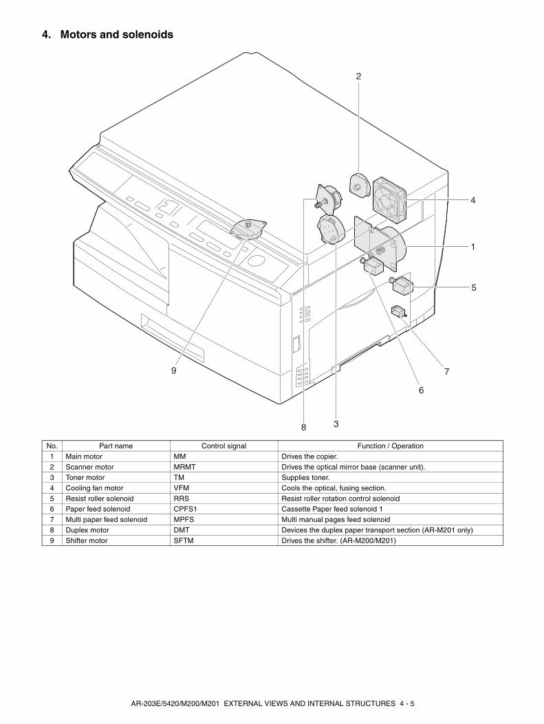
4. Motors and solenoids
4
1
5
3
2
7
6
8
9
No. Part name Control signal Function / Operation
1 Main motor MM Drives the copier.
2 Scanner motor MRMT Drives the optical mirror base (scanner unit).
3 Toner motor TM Supplies toner.
4 Cooling fan motor VFM Cools the optical, fusing section.
5 Resist roller solenoid RRS Resist roller rotation control solenoid6 Paper feed solenoid CPFS1 Cassette Paper feed solenoid 1
7 Multi paper feed solenoid MPFS Multi manual pages feed solenoid
8 Duplex motor DMT Devices the duplex paper transport section (AR-M201 only)
9 Shifter motor SFTM Drives the shifter. (AR-M200/M201)
AR-203E/5420/M200/M201 EXTERNAL VIEWS AND INTERNAL STRUCTURES 4 - 5

5. Sensors and switches
5
6
4
7
21
3
No. Name Signal Type Function Output
1 Scanner unit home position sensor
MHPS Transmission sensor Scanner unit home position detection
"H" at home position
2 POD sensor POD Transmission sensor Paper exit detection "H" at paper pass
3 PPD2 sensor PPD2 Transmission sensor Paper transport detection 2 "L" at paper pass4 Cassette detection switch CED1 Micro-switch Cassette installation detection "H" at cassette insertion
5 PD1 sensor (AR-M200/M201) PD1 Micro-switch Paper width detect "H" at A4 size or less"L" at A4 size or more
6 PPD1 sensor PPD1 Transmission sensor Paper transport detection 1 "L" at paper pass
7 Door switch DSW Micro-switch Door open/close detection (safety switch for 24V)
1 or 0V of 24V at door open
AR-203E/5420/M200/M201 EXTERNAL VIEWS AND INTERNAL STRUCTURES 4 - 6
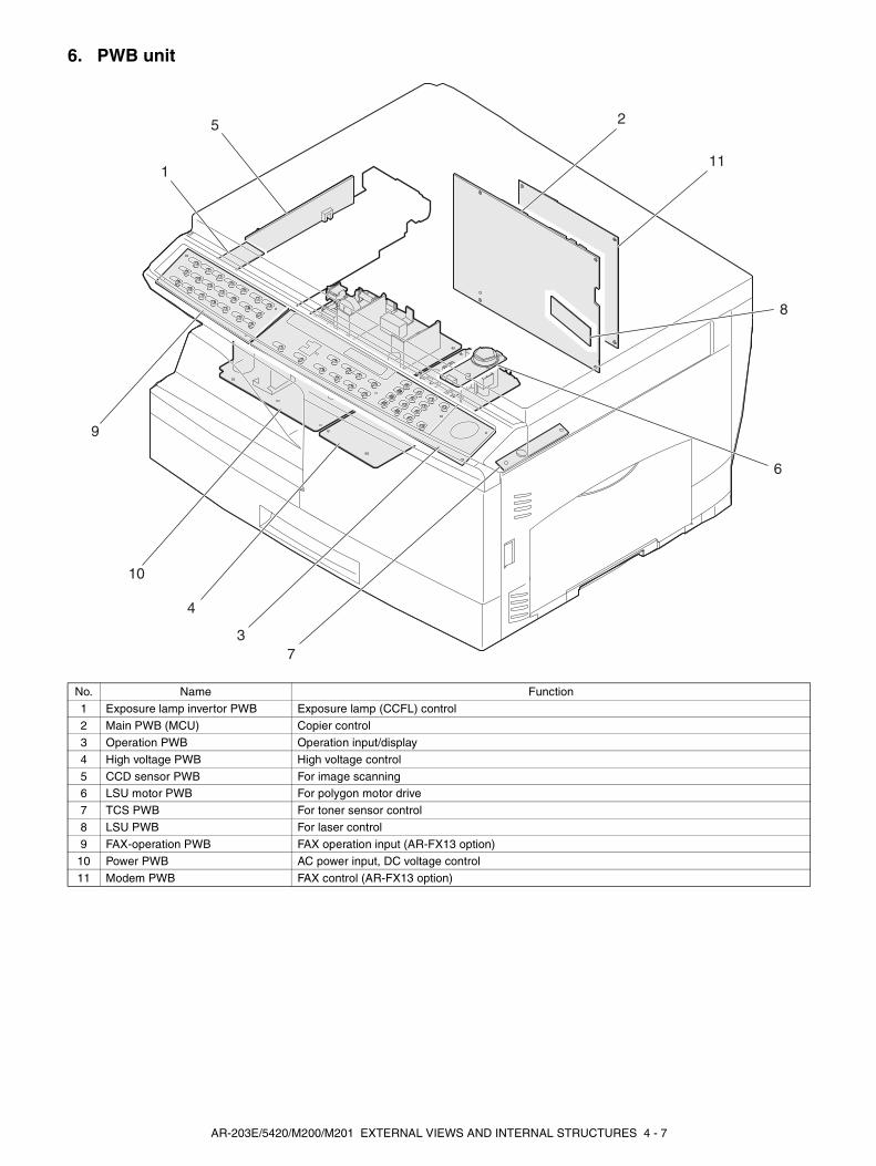
6. PWB unit
1
5 2
11
8
6
37
4
10
9
No. Name Function
1 Exposure lamp invertor PWB Exposure lamp (CCFL) control
2 Main PWB (MCU) Copier control
3 Operation PWB Operation input/display
4 High voltage PWB High voltage control
5 CCD sensor PWB For image scanning6 LSU motor PWB For polygon motor drive
7 TCS PWB For toner sensor control
8 LSU PWB For laser control
9 FAX-operation PWB FAX operation input (AR-FX13 option)
10 Power PWB AC power input, DC voltage control
11 Modem PWB FAX control (AR-FX13 option)
AR-203E/5420/M200/M201 EXTERNAL VIEWS AND INTERNAL STRUCTURES 4 - 7
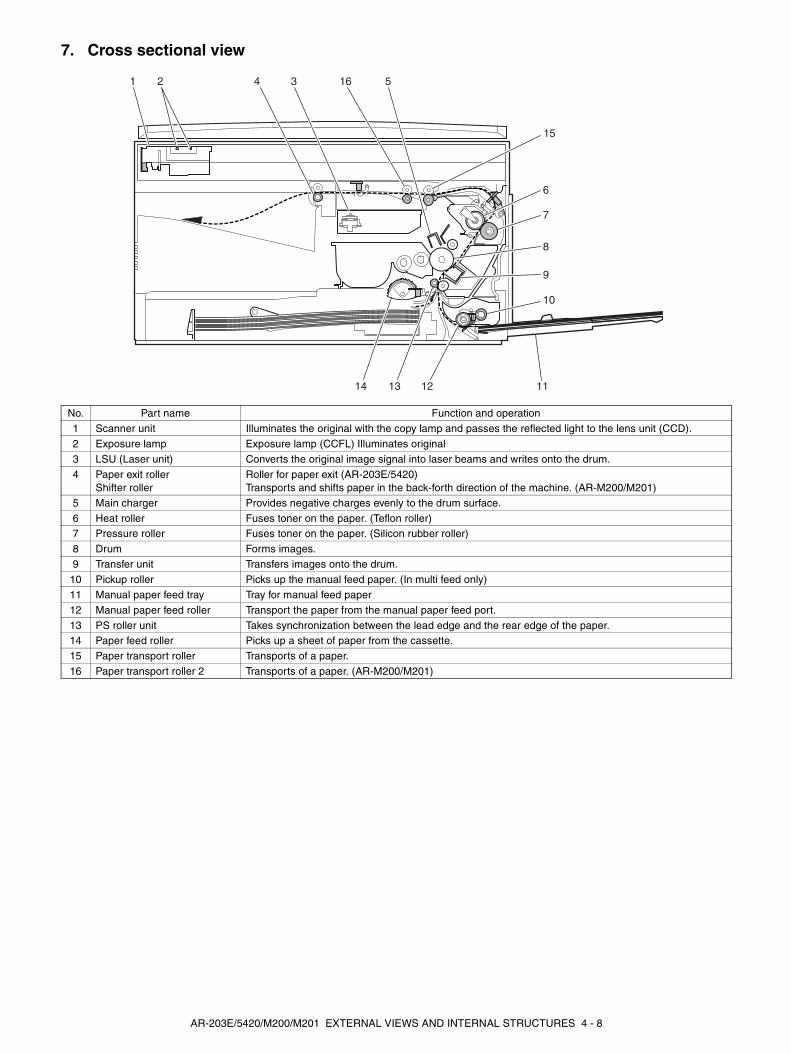
7. Cross sectional view
6
7
8
9
10
111214 13
4 16
15
1 2 53
No. Part name Function and operation
1 Scanner unit Illuminates the original with the copy lamp and passes the reflected light to the lens unit (CCD).
2 Exposure lamp Exposure lamp (CCFL) Illuminates original
3 LSU (Laser unit) Converts the original image signal into laser beams and writes onto the drum.
4 Paper exit rollerShifter roller
Roller for paper exit (AR-203E/5420)Transports and shifts paper in the back-forth direction of the machine. (AR-M200/M201)
5 Main charger Provides negative charges evenly to the drum surface.
6 Heat roller Fuses toner on the paper. (Teflon roller)7 Pressure roller Fuses toner on the paper. (Silicon rubber roller)
8 Drum Forms images.
9 Transfer unit Transfers images onto the drum.
10 Pickup roller Picks up the manual feed paper. (In multi feed only)
11 Manual paper feed tray Tray for manual feed paper
12 Manual paper feed roller Transport the paper from the manual paper feed port.
13 PS roller unit Takes synchronization between the lead edge and the rear edge of the paper.14 Paper feed roller Picks up a sheet of paper from the cassette.
15 Paper transport roller Transports of a paper.
16 Paper transport roller 2 Transports of a paper. (AR-M200/M201)
AR-203E/5420/M200/M201 EXTERNAL VIEWS AND INTERNAL STRUCTURES 4 - 8
[5] UNPACKING AND INSTALLATION
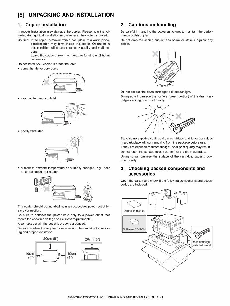
1. Copier installationImproper installation may damage the copier. Please note the fol-lowing during initial installation and whenever the copier is moved.
Caution: If the copier is moved from a cool place to a warm place,condensation may form inside the copier. Operation inthis condition will cause poor copy quality and malfunc-tions.Leave the copier at room temperature for at least 2 hoursbefore use.
Do not install your copier in areas that are:
• damp, humid, or very dusty
• exposed to direct sunlight
• poorly ventilated
• subject to extreme temperature or humidity changes, e.g., nearan air conditioner or heater.
The copier should be installed near an accessible power outlet foreasy connection.
Be sure to connect the power cord only to a power outlet thatmeets the specified voltage and current requirements.
Also make certain the outlet is properly grounded.
Be sure to allow the required space around the machine for servic-ing and proper ventilation.
2. Cautions on handlingBe careful in handling the copier as follows to maintain the perfor-mance of this copier.
Do not drop the copier, subject it to shock or strike it against anyobject.
Do not expose the drum cartridge to direct sunlight.
Doing so will damage the surface (green portion) of the drum car-tridge, causing poor print quality.
Store spare supplies such as drum cartridges and toner cartridgesin a dark place without removing from the package before use.
If they are exposed to direct sunlight, poor print quality may result.
Do not touch the surface (green portion) of the drum cartridge.
Doing so will damage the surface of the cartridge, causing poorprint quality.
3. Checking packed components and accessories
Open the carton and check if the following components and acces-sories are included.
20cm (8")20cm (8")
10cm(4")
10cm(4")
Operation manual
Software CD-ROM
Drum cartridge(installed in unit)
AR-203E/5420/M200/M201 UNPACKING AND INSTALLATION 5 - 1
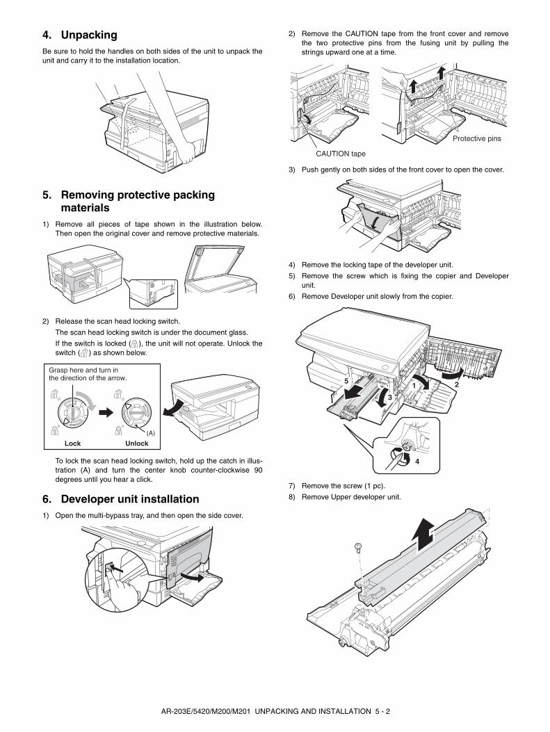
4. UnpackingBe sure to hold the handles on both sides of the unit to unpack theunit and carry it to the installation location.
5. Removing protective packing materials
1) Remove all pieces of tape shown in the illustration below.Then open the original cover and remove protective materials.
2) Release the scan head locking switch.
The scan head locking switch is under the document glass.
If the switch is locked ( ), the unit will not operate. Unlock theswitch ( ) as shown below.
To lock the scan head locking switch, hold up the catch in illus-tration (A) and turn the center knob counter-clockwise 90degrees until you hear a click.
6. Developer unit installation1) Open the multi-bypass tray, and then open the side cover.
2) Remove the CAUTION tape from the front cover and removethe two protective pins from the fusing unit by pulling thestrings upward one at a time.
3) Push gently on both sides of the front cover to open the cover.
4) Remove the locking tape of the developer unit.
5) Remove the screw which is fixing the copier and Developerunit.
6) Remove Developer unit slowly from the copier.
7) Remove the screw (1 pc).
8) Remove Upper developer unit.
(A)
Lock Unlock
Grasp here and turn in the direction of the arrow.
CAUTION tape
Protective pins
2
4
5
3
1
AR-203E/5420/M200/M201 UNPACKING AND INSTALLATION 5 - 2
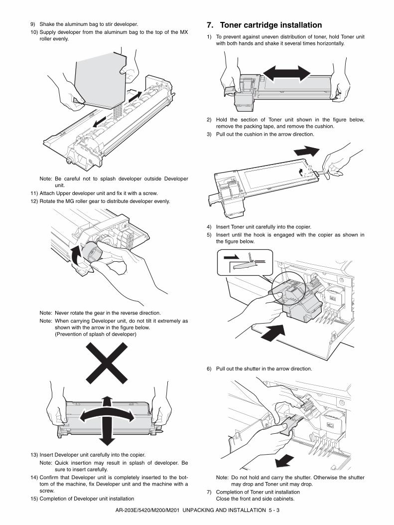
9) Shake the aluminum bag to stir developer.
10) Supply developer from the aluminum bag to the top of the MXroller evenly.
Note: Be careful not to splash developer outside Developerunit.
11) Attach Upper developer unit and fix it with a screw.
12) Rotate the MG roller gear to distribute developer evenly.
Note: Never rotate the gear in the reverse direction.
Note: When carrying Developer unit, do not tilt it extremely asshown with the arrow in the figure below.(Prevention of splash of developer)
13) Insert Developer unit carefully into the copier.
Note: Quick insertion may result in splash of developer. Besure to insert carefully.
14) Confirm that Developer unit is completely inserted to the bot-tom of the machine, fix Developer unit and the machine with ascrew.
15) Completion of Developer unit installation
7. Toner cartridge installation1) To prevent against uneven distribution of toner, hold Toner unit
with both hands and shake it several times horizontally.
2) Hold the section of Toner unit shown in the figure below,remove the packing tape, and remove the cushion.
3) Pull out the cushion in the arrow direction.
4) Insert Toner unit carefully into the copier.
5) Insert until the hook is engaged with the copier as shown inthe figure below.
6) Pull out the shutter in the arrow direction.
Note: Do not hold and carry the shutter. Otherwise the shuttermay drop and Toner unit may drop.
7) Completion of Toner unit installationClose the front and side cabinets.
AR-203E/5420/M200/M201 UNPACKING AND INSTALLATION 5 - 3
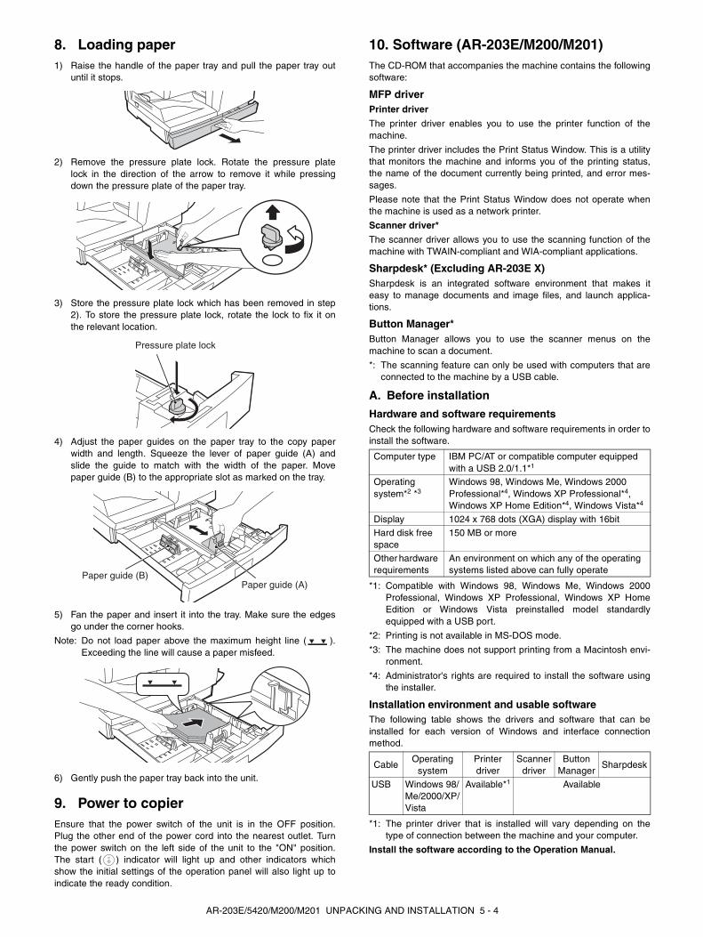
8. Loading paper1) Raise the handle of the paper tray and pull the paper tray out
until it stops.
2) Remove the pressure plate lock. Rotate the pressure platelock in the direction of the arrow to remove it while pressingdown the pressure plate of the paper tray.
3) Store the pressure plate lock which has been removed in step2). To store the pressure plate lock, rotate the lock to fix it onthe relevant location.
4) Adjust the paper guides on the paper tray to the copy paperwidth and length. Squeeze the lever of paper guide (A) andslide the guide to match with the width of the paper. Movepaper guide (B) to the appropriate slot as marked on the tray.
5) Fan the paper and insert it into the tray. Make sure the edgesgo under the corner hooks.
Note: Do not load paper above the maximum height line ( ).Exceeding the line will cause a paper misfeed.
6) Gently push the paper tray back into the unit.
9. Power to copierEnsure that the power switch of the unit is in the OFF position.Plug the other end of the power cord into the nearest outlet. Turnthe power switch on the left side of the unit to the "ON" position.The start ( ) indicator will light up and other indicators whichshow the initial settings of the operation panel will also light up toindicate the ready condition.
10. Software (AR-203E/M200/M201)The CD-ROM that accompanies the machine contains the followingsoftware:
MFP driverPrinter driver
The printer driver enables you to use the printer function of themachine.
The printer driver includes the Print Status Window. This is a utilitythat monitors the machine and informs you of the printing status,the name of the document currently being printed, and error mes-sages.
Please note that the Print Status Window does not operate whenthe machine is used as a network printer.
Scanner driver*
The scanner driver allows you to use the scanning function of themachine with TWAIN-compliant and WIA-compliant applications.
Sharpdesk* (Excluding AR-203E X)Sharpdesk is an integrated software environment that makes iteasy to manage documents and image files, and launch applica-tions.
Button Manager*Button Manager allows you to use the scanner menus on themachine to scan a document.
*: The scanning feature can only be used with computers that areconnected to the machine by a USB cable.
A. Before installation
Hardware and software requirementsCheck the following hardware and software requirements in order toinstall the software.
*1: Compatible with Windows 98, Windows Me, Windows 2000Professional, Windows XP Professional, Windows XP HomeEdition or Windows Vista preinstalled model standardlyequipped with a USB port.
*2: Printing is not available in MS-DOS mode.
*3: The machine does not support printing from a Macintosh envi-ronment.
*4: Administrator's rights are required to install the software usingthe installer.
Installation environment and usable softwareThe following table shows the drivers and software that can beinstalled for each version of Windows and interface connectionmethod.
*1: The printer driver that is installed will vary depending on thetype of connection between the machine and your computer.
Install the software according to the Operation Manual.
Pressure plate lock
Paper guide (B)Paper guide (A)
Computer type IBM PC/AT or compatible computer equipped with a USB 2.0/1.1*1
Operating system*2 *3
Windows 98, Windows Me, Windows 2000 Professional*4, Windows XP Professional*4, Windows XP Home Edition*4, Windows Vista*4
Display 1024 x 768 dots (XGA) display with 16bit
Hard disk free space
150 MB or more
Other hardware requirements
An environment on which any of the operating systems listed above can fully operate
CableOperating
systemPrinter driver
Scanner driver
Button Manager
Sharpdesk
USB Windows 98/Me/2000/XP/Vista
Available*1 Available
AR-203E/5420/M200/M201 UNPACKING AND INSTALLATION 5 - 4
B. Installing the softwareNote:
• The screen images in this manual are mainly for Windows XP.With other versions of Windows, some screen images may be dif-ferent from those in this manual.
• In the following explanations it is assumed that the mouse is con-figured for right hand operation.
• If an error message appears, follow the instructions on the screento solve the problem. After the problem is solved, the installationprocedure will continue. Depending on the problem, you mayhave to click the "Cancel" button to exit the installer. In this case,reinstall the software from the beginning after solving the prob-lem.
1) The USB cable must not be connected to the machine. Makesure that the cable is not connected before proceeding.
If the cable is connected, a Plug and Play window will appear. Ifthis happens, click the "Cancel" button to close the window anddisconnect the cable.
Note: The cable will be connected in step 13).
2) Insert the CD-ROM into your computer's CD-ROM drive.
3) Click the "start" button, click "My Computer", and then double-click the CD-ROM icon.
• In Windows Vista, click the "Start" button, click "Computer",and then double-click the CD-ROM icon.
• In Windows 98/Me/2000, double-click "My Computer", andthen double-click the CD-ROM icon.
4) Double-click the "setup" icon.
In Windows Vista, if a message screen appears asking you forconfirmation, click "Allow".
5) The "SOFTWARE LICENSE" window will appear. Make surethat you understand the contents of the software license, andthen click the "Yes" button.
Note: You can show the "SOFTWARE LICENSE" in a differentlanguage by selecting the desired language from thelanguage menu. To install the software in the selectedlanguage, continue the installation with that languageselected.
6) Read the "Readme First" in the "Welcome" window and thenclick the "Next" button.
7) To install all of the software, click the "Standard" button and goto step 12).
To install particular packages, click the "Custom" button and goto next step.
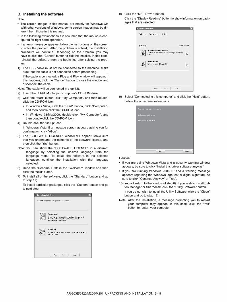
8) Click the "MFP Driver" button.
Click the "Display Readme" button to show information on pack-ages that are selected.
9) Select "Connected to this computer" and click the "Next" button.
Follow the on-screen instructions.
Caution:
• If you are using Windows Vista and a security warning windowappears, be sure to click "Install this driver software anyway".
• If you are running Windows 2000/XP and a warning messageappears regarding the Windows logo test or digital signature, besure to click "Continue Anyway" or "Yes".
10) You will return to the window of step 8). If you wish to install But-ton Manager or Sharpdesk, click the "Utility Software" button.
If you do not wish to install the Utility Software, click the "Close"button and go to step 12).
Note: After the installation, a message prompting you to restartyour computer may appear. In this case, click the "Yes"button to restart your computer.
AR-203E/5420/M200/M201 UNPACKING AND INSTALLATION 5 - 5

Installing the Utility Software
11) Click the "Button Manager" or the "Sharpdesk" button.
Click the "Display Readme" button to show information on pack-ages that are selected.
Follow the on-screen instructions.
Caution: In Windows 98/Me/2000, if the following screen appears,click the "Skip" button or the "Continue" button as appro-priate to continue the Sharpdesk installation.
If "Skip" is selected, the Sharpdesk installation will con-tinue without installing Sharpdesk Imaging.
If "Continue" is selected, Sharpdesk Imaging will beinstalled. If Imaging for Windows is installed on your com-puter, Sharpdesk Imaging will overwrite Imaging for Win-dows.
12) When installing is finished, click the "Close" button.
Caution:
• If you are using Windows Vista and a security warning windowappears, be sure to click "Install this driver software anyway".
• If you are running Windows 2000/XP and a warning messageappears regarding the Windows logo test or digital signature, besure to click "Continue Anyway" or "Yes".
A message will appear instructing you to connect the machineto your computer. Click the "OK" button.
Note: After the installation, a message prompting you to restartyour computer may appear. In this case, click the "Yes"button to restart your computer.
13) Make sure that the power of the machine is turned on, and thenconnect the USB cable.
Windows will detect the machine and a Plug and Play screenwill appear.
14) Follow the instructions in the plug and play window to install thedriver.
Follow the on-screen instructions.
Caution:
• If you are using Windows Vista and a security warning windowappears, be sure to click "Install this driver software anyway".
• If you are running Windows 2000/XP and a warning messageappears regarding the Windows logo test or digital signature, besure to click "Continue Anyway" or "Yes".
This completes the installation of the software.
• If you installed Button Manager, set up Button Manager asexplained in "C. Setting up Button Manager".
• If you installed Sharpdesk, the Sharpdesk setup screen willappear. Follow the instructions in the screen to set up Sharpdesk.
(1) Connecting a USB cableFollow the procedure below to connect the machine to your com-puter.
A USB cable for connecting the machine to your computer is notincluded with the machine. Please purchase the appropriate cablefor your computer.
Caution:
• USB is available with a PC/AT compatible computer that was orig-inally equipped with USB and had Windows 98, Windows Me,Windows 2000 Professional, Windows XP or Windows Vista pre-installed.
• Do not connect the USB cable before installing the printer driver.The USB cable should be connected during installation of theprinter driver.
Note
• If the machine will be connected using a USB 2.0 port of yourcomputer, please purchase a USB cable that supports USB 2.0.
• To obtain the fastest USB 2.0 data transfer speed, "USB2.0MODE SWITCH" in the machine's user programs must be set to"HI-SPEED". For more information, see "[12] USER PROGRAM".(AR-M200/M201 only)
• Use the machine's "HI-SPEED" mode only when using a com-puter that is running Windows 2000/XP/Vista.
• Even when the Microsoft USB 2.0 driver is used, it may not bepossible to obtain full USB 2.0 speed if a PC card supportingUSB 2.0 is used. To obtain the latest driver (which may enable ahigher speed), contact the manufacturer of your PC card.
• Connection is also possible using a USB 1.1 port on your com-puter.However, the specifications will be USB 1.1 specifications (Full-Speed).
1) Insert the cable into the USB connector on the machine.
2) Insert the other end of the cable into your computer's USB port.
(AR-203E) (AR-M200/M201)
AR-203E/5420/M200/M201 UNPACKING AND INSTALLATION 5 - 6
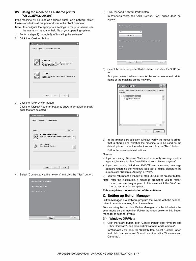
(2) Using the machine as a shared printer (AR-203E/M200/M201)
If the machine will be used as a shared printer on a network, followthese steps to install the printer driver in the client computer.
Note: To configure the appropriate settings in the print server, seethe operation manual or help file of your operating system.
1) Perform steps 2) through 6) in "Installing the software".
2) Click the "Custom" button.
3) Click the "MFP Driver" button.
Click the "Display Readme" button to show information on pack-ages that are selected.
4) Select "Connected via the network" and click the "Next" button.
5) Click the "Add Network Port" button.
In Windows Vista, the "Add Network Port" button does notappear.
6) Select the network printer that is shared and click the "OK" but-ton.
Ask your network administrator for the server name and printername of the machine on the network.
7) In the printer port selection window, verify the network printerthat is shared and whether the machine is to be used as thedefault printer, make the selections and click the "Next" button.
Follow the on-screen instructions.
Caution:
• If you are using Windows Vista and a security warning windowappears, be sure to click "Install this driver software anyway".
• If you are running Windows 2000/XP and a warning messageappears regarding the Windows logo test or digital signature, besure to click "Continue Anyway" or "Yes".
8) You will return to the window of step 3). Click the "Close" button.
Note: After the installation, a message prompting you to restartyour computer may appear. In this case, click the "Yes" but-ton to restart your computer.
This completes the installation of the software.
C. Setting up Button ManagerButton Manager is a software program that works with the scannerdriver to enable scanning from the machine.
To scan using the machine, Button Manager must be linked with thescan menu on the machine. Follow the steps below to link ButtonManager to scanner events.
(1) Windows XP/Vista1) Click the "start" button, click "Control Panel", click "Printers and
Other Hardware", and then click "Scanners and Cameras".
In Windows Vista, click the "Start" button, select "Control Panel"and click "Hardware and Sound", and then click "Scanners andCameras".
AR-203E/5420/M200/M201 UNPACKING AND INSTALLATION 5 - 7
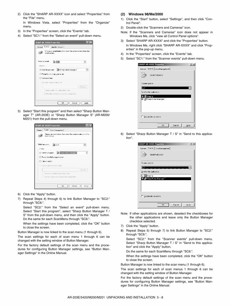
2) Click the "SHARP AR-XXXX" icon and select "Properties" fromthe "File" menu.
In Windows Vista, select "Properties" from the "Organize"menu.
3) In the "Properties" screen, click the "Events" tab.
4) Select "SC1:" from the "Select an event" pull-down menu.
5) Select "Start this program" and then select "Sharp Button Man-ager T" (AR-203E) or "Sharp Button Manager S" (AR-M200/M201) from the pull-down menu.
6) Click the "Apply" button.
7) Repeat Steps 4) through 6) to link Button Manager to "SC2:"through "SC6:".
Select "SC2:" from the "Select an event" pull-down menu.Select "Start this program", select "Sharp Button Manager T /S" from the pull-down menu, and then click the "Apply" button.Do the same for each ScanMenu through "SC6:".
When the settings have been completed, click the "OK" buttonto close the screen.
Button Manager is now linked to the scan menu (1 through 6).
The scan settings for each of scan menu 1 through 6 can bechanged with the setting window of Button Manager.
For the factory default settings of the scan menu and the proce-dures for configuring Button Manager settings, see "Button Man-ager Settings" in the Online Manual.
(2) Windows 98/Me/20001) Click the "Start" button, select "Settings", and then click "Con-
trol Panel".
2) Double-click the "Scanners and Cameras" icon.
Note: If the "Scanners and Cameras" icon does not appear inWindows Me, click "view all Control Panel options".
3) Select "SHARP AR-XXXX" and click the "Properties" button.
In Windows Me, right click "SHARP AR-XXXX" and click "Prop-erties" in the pop-up menu.
4) In the "Properties" screen, click the "Events" tab.
5) Select "SC1:" from the "Scanner events" pull-down menu.
6) Select "Sharp Button Manager T / S" in "Send to this applica-tion".
Note: If other applications are shown, deselect the checkboxes forthe other applications and leave only the Button Managercheckbox selected.
7) Click the "Apply" button.
8) Repeat Steps 5) through 7) to link Button Manager to "SC2:"through "SC6:".
Select "SC2:" from the "Scanner events" pull-down menu.Select "Sharp Button Manager T / S" in "Send to this applica-tion" and click the "Apply" button.
Do the same for each ScanMenu through "SC6:".
When the settings have been completed, click the "OK" buttonto close the screen.
Button Manager is now linked to the scan menu (1 through 6).
The scan settings for each of scan menus 1 through 6 can bechanged with the setting window of Button Manager.
For the factory default settings of the scan menu and the proce-dures for configuring Button Manager settings, see "Button Man-ager Settings" in the Online Manual.
AR-203E/5420/M200/M201 UNPACKING AND INSTALLATION 5 - 8

11. InterfaceA. USB
ConnectorType-B connector
CableShielded twisted pair cable
(2 m (6 feet) Max.: high-speed transmission equivalent)
Pin configurationThe pin numbers and signal names are listed in the following table.
12. MovingMoving instructionsWhen moving the unit, follow the procedure below.
Note: When moving this unit, be sure to remove the toner cartridgein advance.
1) Turn the power switch off and remove the power cord from theoutlet.
2) Open the side cover and front cover, in that order. Remove thetoner cartridge and close the front cover and side cover, in thatorder.
To open and close the side cover and front cover, and to removethe toner cartridge.
3) Raise the handle of the paper tray and pull the paper tray outuntil it stops.
4) Push the center of the pressure plate down until it locks in placeand lock the plate using the pressure plate lock which has beenstored in the front of the paper tray.
5) Push the paper tray back into the unit.
6) Lock the scan head locking switch.
Note: When shipping the unit, the scan head locking switch mustbe locked to prevent shipping damage.
7) Close the multi-bypass tray and the paper output tray extension,and attach the packing materials and tape which were removedduring installation of the unit.
8) Pack the unit into the carton.
13. Scanner moisture-proof kitIf the machine is installed in a highly humid environment, you canalleviate dew condensation inside the scanner by installing thescanner moisture-proof kit described below.
A. ComponentsScanner moisture-proof kit (DKIT-0016QSZZ)
B. Precautions at installationClean the position where each cushion/mylar is attached withindustrial alcohol before the work.
C. Attachment methodTurn the main switch to the "OFF" position and remove the powerplug from the outlet.
1) Remove the document cover.
Remove the document cover from the copier.
2) Remove the rear cabinet.
Remove the four screws and then remove the rear cabinet.
Pin No. Signal name
1 +5V
2 -DATA
3 +DATA
4 GND
12
3 4
Name Part code Qty
1 Scanner condensation prevention mylar
PSHEZ0493QSZZ 3
2 Optical right hole mylar B PSHEZ0469QSZZ 2
3 Scanner motor metal plate cushion
PMLT-0106QSZZ 2
4 Scanner upper surface cushion PMLT-0105QSZZ 1
5 Scanner motor lower mylar PSHEP0600QSZZ 1
6 Scanner UPG mylar J3 PSHEP0599QSZZ 17 Fan housing cushion PMLT-0108QSZ1 1
1
2
AR-203E/5420/M200/M201 UNPACKING AND INSTALLATION 5 - 9
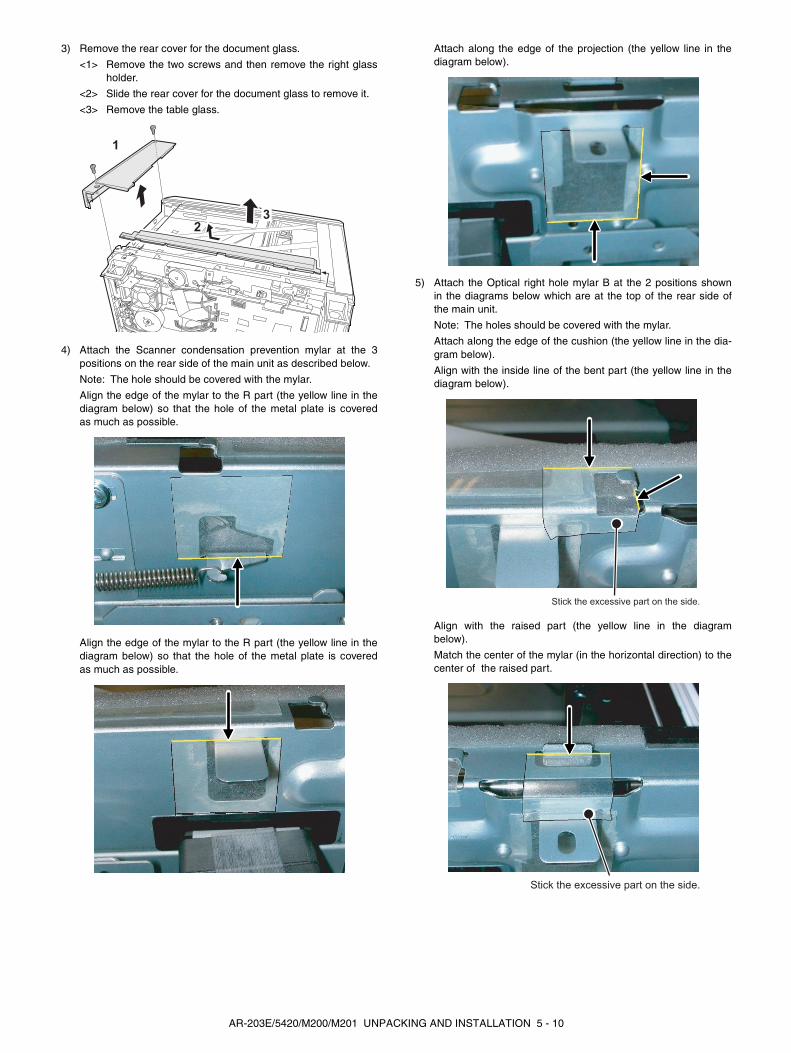
3) Remove the rear cover for the document glass.
<1> Remove the two screws and then remove the right glassholder.
<2> Slide the rear cover for the document glass to remove it.
<3> Remove the table glass.
4) Attach the Scanner condensation prevention mylar at the 3positions on the rear side of the main unit as described below.
Note: The hole should be covered with the mylar.
Align the edge of the mylar to the R part (the yellow line in thediagram below) so that the hole of the metal plate is coveredas much as possible.
Align the edge of the mylar to the R part (the yellow line in thediagram below) so that the hole of the metal plate is coveredas much as possible.
Attach along the edge of the projection (the yellow line in thediagram below).
5) Attach the Optical right hole mylar B at the 2 positions shownin the diagrams below which are at the top of the rear side ofthe main unit.
Note: The holes should be covered with the mylar.
Attach along the edge of the cushion (the yellow line in the dia-gram below).
Align with the inside line of the bent part (the yellow line in thediagram below).
Align with the raised part (the yellow line in the diagrambelow).
Match the center of the mylar (in the horizontal direction) to thecenter of the raised part.
1
2
3
Stick the excessive part on the side.
Stick the excessive part on the side.
AR-203E/5420/M200/M201 UNPACKING AND INSTALLATION 5 - 10
6) Attach the Scanner motor metal plate cushion at 1 position onthe attachment plate of the motor on the rear side of the mainunit.
Note: The hole on the top of the motor unit should be coveredwith the mylar.
Align the edge of the metal plate and the edge of the cushion(the yellow line in the diagram below).
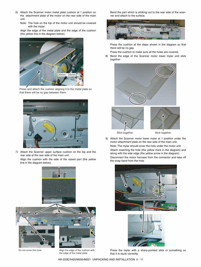
7) Attach the Scanner upper surface cushion on the top and therear side at the rear side of the main unit.
Align the cushion with the side of the raised part (the yellowline in the diagram below).
Bend the part which is sticking out to the rear side of the scan-ner and attach to the surface.
Press the cushion at the steps shown in the diagram so thatthere will be no gap.
Press the cushion to make sure all the holes are covered.
8) Bend the edge of the Scanner motor lower mylar and sticktogether.
9) Attach the Scanner motor lower mylar at 1 position under themotor attachment plate on the rear side of the main unit.
Note: The mylar should cover the hole under the motor unit.
Attach matching the hole (the yellow mark in the diagram) andalong with the side edge (the yellow arrow in the diagram).
Disconnect the motor harness from the connector and take offthe snap band from the hole.
Press the mylar with a sharp-pointed stick or something sothat it is stuck correctly.
Press and attach the cushion aligning it to the metal plate so
that there will be no gap between them.
20mm - 25mm
Do not cover this hole. Align the edge of the cushion with
the edge of the metal plate.
Stick together. Stick together.
AR-203E/5420/M200/M201 UNPACKING AND INSTALLATION 5 - 11
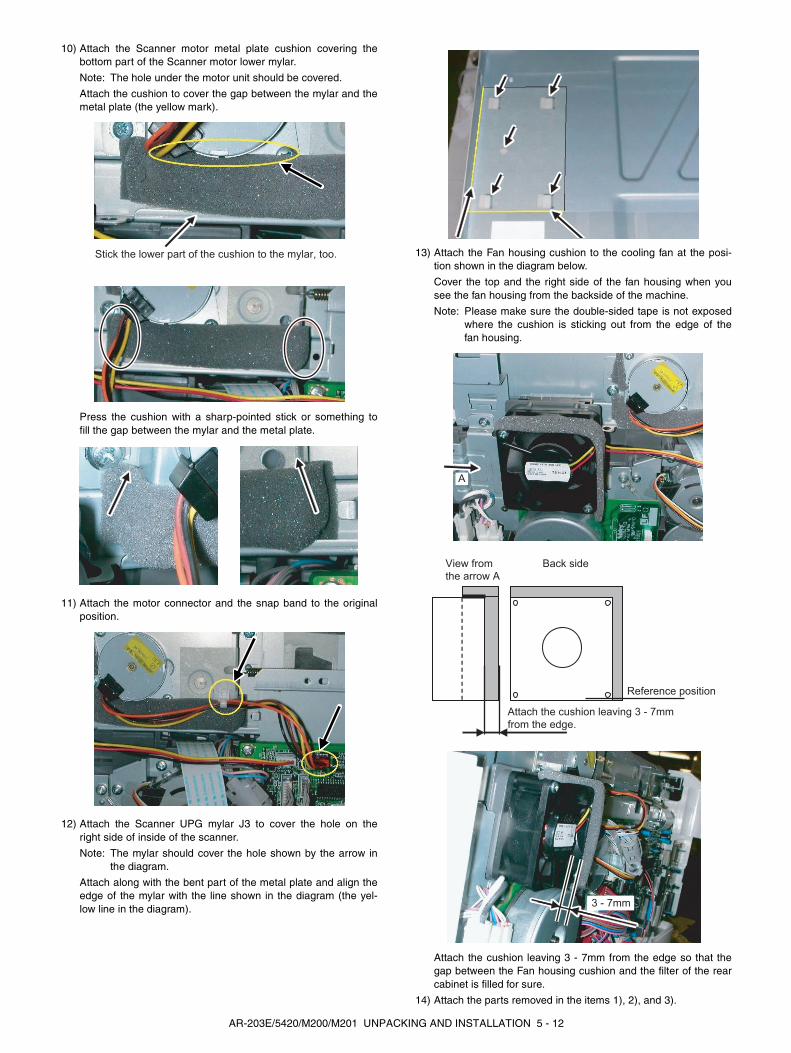
10) Attach the Scanner motor metal plate cushion covering thebottom part of the Scanner motor lower mylar.
Note: The hole under the motor unit should be covered.
Attach the cushion to cover the gap between the mylar and themetal plate (the yellow mark).
Press the cushion with a sharp-pointed stick or something tofill the gap between the mylar and the metal plate.
11) Attach the motor connector and the snap band to the originalposition.
12) Attach the Scanner UPG mylar J3 to cover the hole on theright side of inside of the scanner.
Note: The mylar should cover the hole shown by the arrow inthe diagram.
Attach along with the bent part of the metal plate and align theedge of the mylar with the line shown in the diagram (the yel-low line in the diagram).
13) Attach the Fan housing cushion to the cooling fan at the posi-tion shown in the diagram below.
Cover the top and the right side of the fan housing when yousee the fan housing from the backside of the machine.
Note: Please make sure the double-sided tape is not exposedwhere the cushion is sticking out from the edge of thefan housing.
Attach the cushion leaving 3 - 7mm from the edge so that thegap between the Fan housing cushion and the filter of the rearcabinet is filled for sure.
14) Attach the parts removed in the items 1), 2), and 3).
Stick the lower part of the cushion to the mylar, too.
A
View from
the arrow A
Back side
Attach the cushion leaving 3 - 7mm
from the edge.
Reference position
3 - 7mm
AR-203E/5420/M200/M201 UNPACKING AND INSTALLATION 5 - 12
[6] COPY PROCESS
1. Functional diagram
(Basic operation cycle)
(20 microns thick)
Aluminum drum
Pigment layer (0.2to 0.3 microns thick)
An OPC drum is used for the photoconductor.(Structure of the OPC drum layers)
OPC layer
Main charger
Laser beam
MG roller
Cleaning blade
Drum
Transfer unit
Resist roller
ExposureMain high voltage unit
Saw tooth Charge
DrumCleaning
Cleaning blade
Waste toner box
Paper release Fusing Separation
Heat roller
Heater lamp
Transfer
Transfer charger
Transfer highvoltage unit
Developing
Toner
Developer
Print process
Paper transport route
Semiconductor laser
Manual feed
PS roller
Focus correction lens
Electrode
Synchronizationwith drum
Cassettepaper feed
To facedown tray
AR-203E/5420/M200/M201 COPY PROCESS 6 - 1

2. Outline of print processThis printer is a non-impact printer that uses a semiconductorlaser and electrostatic print process. This printer uses an OPC(Organic Photo Conductor) for its photoconductive material.
First, voltage from the main corona unit charges the drum surfaceand a latent image is formed on the drum surface using a laserbeam. This latent image forms a visible image on the drum surfacewhen toner is applied. The toner image is then transferred onto theprint paper by the transfer corona and fused on the print paper inthe fusing section with a combination of heat and pressure.
Step-1: Charge
Step-2: Exposure
∗ Latent image is formed on the drum.
Step-3: DevelopingLatent image formed on the drum is then changed intovisible image with toner.
Step-4: TransferThe visible image (toner image) on the drum is transferredonto the print paper.
Step-5: CleaningResidual toner on the drum surface is removed and col-lected by the cleaning blade.
Step-6: Optical dischargeResidual charge on the drum surface is removed, bysemiconductor laser beam.
3. Actual print processStep-1: DC charge
A uniform negative charge is applied over the OPC drum surfaceby the main charging unit. Stable potential is maintained by meansof the Scorotron charger.
Positive charges are generated in the aluminum layer.
Step-2: Exposure (laser beam, lens)
A Laser beam is generated from the semiconductor laser and con-trolled by the print pattern signal. The laser writes onto the OPCdrum surface through the polygon mirrors and lens. The resis-tance of the OPC layer decreases for an area exposed by the laserbeam (corresponding to the print pattern signal). The beam neu-tralizes the negative charge. An electrostatic latent image isformed on the drum surface.
AboutDC5.5KV
( 580V/ 400V)
OPC layerPigmentlayerAluminumdrum
OPC layerPigmentlayerAluminumlayer
Drum surface chargeafter the exposure
Non-image area Image area
Semiconductor laser
Exposure(semiconductor laser)
AR-203E/5420/M200/M201 COPY PROCESS 6 - 2
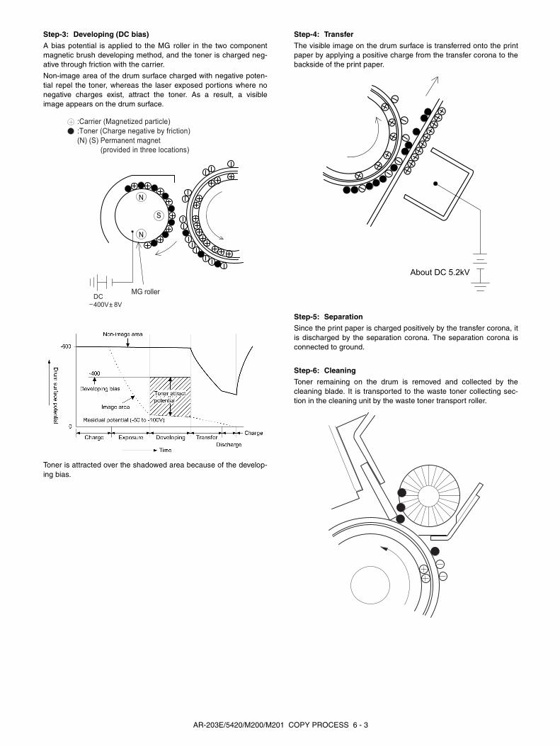
Step-3: Developing (DC bias)
A bias potential is applied to the MG roller in the two componentmagnetic brush developing method, and the toner is charged neg-ative through friction with the carrier.
Non-image area of the drum surface charged with negative poten-tial repel the toner, whereas the laser exposed portions where nonegative charges exist, attract the toner. As a result, a visibleimage appears on the drum surface.
Toner is attracted over the shadowed area because of the develop-ing bias.
Step-4: Transfer
The visible image on the drum surface is transferred onto the printpaper by applying a positive charge from the transfer corona to thebackside of the print paper.
Step-5: Separation
Since the print paper is charged positively by the transfer corona, itis discharged by the separation corona. The separation corona isconnected to ground.
Step-6: Cleaning
Toner remaining on the drum is removed and collected by thecleaning blade. It is transported to the waste toner collecting sec-tion in the cleaning unit by the waste toner transport roller.
S
N
N
:Carrier (Magnetized particle):Toner (Charge negative by friction)(N) (S) Permanent magnet
(provided in three locations)
MG roller
DC400V 8V
About DC 5.2kV
AR-203E/5420/M200/M201 COPY PROCESS 6 - 3

Step-7: Optical discharge (Semiconductor laser)
Before the drum rotation is stopped, the semiconductor laser isradiated onto the drum to reduce the electrical resistance in theOPC layer and eliminate residual charge, providing a uniform stateto the drum surface for the next page to be printed.
When the electrical resistance is reduced, positive charges on thealuminum layer are moved and neutralized with negative chargeson the OPC layer.
Charge by the Scorotron charger
Function
The Scorotron charger functions to maintain uniform surfacepotential on the drum at all times, It control the surface potentialregardless of the charge characteristics of the photoconductor.
Basic function
A screen grid is placed between the saw tooth and the photocon-ductor. A stable voltage is added to the screen grid to maintain thecorona current on the photoconductor.
As the photoconductor is charged by the saw tooth from the maincorona unit, the surface potential increases. This increases thecurrent flowing through the screen grid. When the photoconductorpotential nears the grid potential, the current turns to flow to thegrid so that the photoconductor potential can be maintained at astable level.
Process controlling
Function
The print pattern signal is converted into an invisible image by thesemiconductor laser using negative to positive (reversible) devel-oping method. Therefore, if the developing bias is added beforethe drum is charged, toner is attracted onto the drum. If the devel-oping bias is not added when the drum is charged, the carrier isattracted to the drum because of the strong electrostatic force ofthe drum.
To avoid this, the process is controlled by adjusting the drumpotential and the grid potential of the Scorotron charger.
Basic function
Voltage added to the screen grid can be selected, high and low. Tomake it easily understood, the figure below shows voltage transi-tion at the developer unit.
Start1) Because the grid potential is at a low level, the drum potential
is at about -400V. (Carrier may not be attracted though the car-rier is pulled towards the drum by the electrostatic force of -400V.
2) Developing bias (-400V) is applied when the photoconductorpotential is switched from LOW to HIGH.
3) Once developing bias (-400V) is applied and the photo con-ductor potential rises to HIGH, toner will not be attracted to thedrum.
StopThe reverse sequence takes place.
Retaining developing bias at an abnormal occurrence
Function
The developing bias will be lost if the power supply was removedduring print process. In this event, the drum potential slightlyabates and the carrier makes deposits on the drum because ofstrong static power. To prevent this, the machine incorporates afunction to retain the developing bias for a certain period anddecrease the voltage gradually against possible power loss.
Basic function
Normally, the developing bias voltage is retained for a certain timebefore the drum comes to a complete stop if the machine shouldstop before completing the normal print cycle. The developing biascan be added before resuming the operation after an abnormalinterruption. Therefore, carrier will not make a deposit on the drumsurface.
Semiconductor laser
0START STOP
Print potential
Toner attractpotential
2)
3)
1) Low
4) High Drum potential
Developing bias
Time
AR-203E/5420/M200/M201 COPY PROCESS 6 - 4

[7] OPERATIONAL DESCRIPTIONS
1. Outline of operationThe outline of operation is described referring to the basic configuration.
(Basic configuration)
(Outline of copy operation)Setting conditions
1) Set copy conditions such as the copy quantity and the copydensity with the operation section, and press the COPY but-ton. The information on copy conditions is sent to the MCU.
Image scanning
2) When the COPY button is pressed, the scanner section startsscanning of images. The light from the copy lamp is reflected by the document andpassed through the lens to the CCD.
Photo signal/Electric signal conversion
3) The image is converted into electrical signals by the CCD cir-cuit and passed to the MCU.
Image process
4) The document image signal sent from the CCD circuit is pro-cessed under the revised conditions and sent to the LSU(laser unit) as print data.
Electric signal/Photo signal (laser beam) conversion
5) The LSU emits laser beams according to the print data.(Electrical signals are converted into photo signals.)
6) The laser beams are radiated through the polygon mirror andvarious lenses to the OPC drum.
Printing
7) Electrostatic latent images are formed on the OPC drumaccording to the laser beams, and the latent images are devel-oped to be visible images (toner images).
8) Meanwhile the paper is fed to the image transfer section insynchronization with the image lead edge.
9) After the transfer of toner images onto the paper, the tonerimages are fused to the paper by the fusing section. The cop-ied paper is discharged onto the exit tray.
(Outline of printer operation)The print data sent from the PC are passed through the NIC PWB(in case of network connection) and the MCU to the LSU. The pro-cedures after that are the same as above 5) and later.
(Outline of scanner operation)The scan data are passed through the MCU to the PC accordingto the conditions requested by the operations with the operationpanel.
Operationsection
Scanner section
CCD
MCU (Main control/image process section) Printer/Scanner I/F
USB
USB
USB
PC
Laser beamPaper exit
Fusing section
Paper transport section
Manual paperfeed section
Cassette paperfeed section
Printer section
LSU (Laser unit)Laser diode, Polygon mirror lens
Process section
FAX modemFAX
(Option)
(Option)Network
FAX I/FNetworkBox
AR-M200/M201
AR-203E/M200/M201
AR-203E/5420/M200/M201 OPERATIONAL DESCRIPTIONS 7 - 1

2. Scanner sectionA. Scanner unitThe scanner unit in the digital copier scans images.
It is composed of the optical unit and the drive unit. The optical unitperforms scanning in the main scan direction with the light receiv-ing elements (color CCD). The drive unit performs scanning in thesub scanning direction by moving the optical unit.
B. Optical systemTwo white lamps are used as the light source.
Light radiated from the light source is applied to the document onthe document table. The reflected light from the document isreflected 4 times by No. 1 - No. 3 mirrors and passed through thereduction lens to form images on the light-receiving surface of 3-line CCD.
The light-receiving surface of the color CCD is provided with 3 linescanning sections for RGB. Separate images scanned in eachcolor section are overlapped to complete color scanning. (WhenPC scanning)
The resolution is 600dpi.
When copying, only the green component is used to print with theprinter.
The color component for printing can be switched to red or blue bythe service simulation.
(Spectrum characteristics of the lamp)
(Spectrum characteristics of the color CCD)
(Optical unit)
C. Drive systemThe drive system is composed of the scanner motor, the pulleygear, the idle pulley, the idle gear, the belt 473, the belt 190, and theshaft.
The motor rotation is converted into reciprocated movements of thebelt 473 through the idle gear, the pulley gear, the belt 190, and theidle pulley to drive the optical unit.
100
75
5045.4
100.0
50.2
25
380 480 580 680 780
Wavelength [nm]
Sen
sitiv
ity
1 Table glass 2 Optical unit 3 Lens4 Mirror 1 5 Mirror 2 6 Mirror 37 CCD PWB 8 Lamp 9 Reflector
10 Original
Spectral sensitivity characteristics (Standard characteristics)
Re
lative
se
nsitiv
ity
Wavelength [nm]
89 98101
7
53 4 2
6
7 9
3 4 6 2 8 5
1
3
1 Scanner motor 2 Pulley gear 3 Idle pulley4 Belt 473 5 Belt 190 6 Optical unit
7 Shaft 8 Idle gear 9 Table glass
AR-203E/5420/M200/M201 OPERATIONAL DESCRIPTIONS 7 - 2
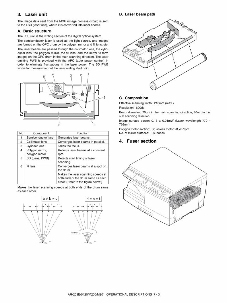
3. Laser unitThe image data sent from the MCU (image process circuit) is sentto the LSU (laser unit), where it is converted into laser beams.
A. Basic structureThe LSU unit is the writing section of the digital optical system.
The semiconductor laser is used as the light source, and imagesare formed on the OPC drum by the polygon mirror and fθ lens, etc.
The laser beams are passed through the collimator lens, the cylin-drical lens, the polygon mirror, the fθ lens, and the mirror to formimages on the OPC drum in the main scanning direction. The laseremitting PWB is provided with the APC (auto power control) inorder to eliminate fluctuations in the laser power. The BD PWBworks for measurement of the laser writing start point.
Makes the laser scanning speeds at both ends of the drum sameas each other.
B. Laser beam path
C. CompositionEffective scanning width: 216mm (max.)
Resolution: 600dpi
Beam diameter: 75um in the main scanning direction, 80um in thesub scanning direction
Image surface power: 0.18 ± 0.01mW (Laser wavelength 770 -795nm)
Polygon motor section: Brushless motor 20.787rpmNo. of mirror surfaces: 5 surfaces
4. Fuser section
No Component Function1 Semiconductor laser Generates laser beams.2 Collimator lens Converges laser beams in parallel.3 Cylinder lens Takes the focus.4 Polygon mirror,
polygon motorReflects laser beams at a constant rpm.
5 BD (Lens, PWB) Detects start timing of laser scanning.
6 fθ lens Converges laser beams at a spot on the drum.Makes the laser scanning speeds at both ends of the drum same as each other. (Refer to the figure below.)
2
3
3
6
4 1
5
6
a ≠ b ≠ ca b c
d = e = fd e f
fθ LENS
AR-203E/5420/M200/M201 OPERATIONAL DESCRIPTIONS 7 - 3

A. General descriptionGeneral block diagram (cross section)
Top view
(1) Heat rollerA Teflon roller is used for the heat roller and a silicone rubber rolleris used for the lower heat roller for better toner fusing performanceand paper separation.
(2) Separator pawlThree separator pawls are used on the upper heat roller. The sep-arator pawls are Teflon coated to reduce friction with the roller andprevent a smear on the paper caused by the separator pawl.
(3) Thermal control1) The heater lamp, thermistor, main PWB, DC power supply
PWB, and triac within the power supply unit are used to controlthe temperature in the fuser unit.To prevent against abnormally high temperature in the fuserunit, a thermal breaker and thermal fuse are used for safetypurposes.
2) The surface temperature of the upper heat roller is set to 160 -200°C. The surface temperature during the power save modeis set to 100°C.
3) The self-check function comes active when one of the follow-ing malfunctions occurs, and an "H" is displayed on the multi-copy window.
a. When the heat roller surface temperature rises above 240°C.
b. When the heat roller surface temperature drops below 100°Cduring the copy cycle.
c. Open thermistor
d. Open thermal fuse
e. When the heat roller temperature does not reach 190°C within27 second after supplying the power.
(4) Fusing resistorThis model is provided with a fusing resistor in the fusing sectionto improve transfer efficiency.
Since the upper heat roller is conductive, when using copy paperthat contains moisture and the distance between the transfer unitand the fusing unit is short, the transfer current may find a path toground via the copy paper, the upper heat roller and the discharg-ing brush.
5. Paper feed section and paper transport section
A. Paper transport path and general operations
Paper feed is made in two ways; the tray paper feed and the man-ual paper feed. The tray is of universal-type, and has the capacityof 250 sheets.
The front loading system allows you to install or remove the trayfrom the front cabinet.
The general descriptions on the tray paper feed and the manualpaper feed operation are given below.
Separator pawl
Separator pawl
PPD2
Thermal fuse
Thermistor
Heat roller
Paper guide
Pressure roller
Heat rollerThermistor
Thermal fuse
Heater lamp
Separator pawl
Safety device(thermal breaker, thermalfuse)
Triac (in thepower supply unit)
Heated by the heater lamp. (950W)
The surface temperatureof the upper heat roller issensed by the thermistor.
Level of the thermistor iscontrolled by the main PWB.
With the signal from themain PWB, the triac iscontrolled on and off.(power supply PWB)
1 Scanner unit 9 Transfer unit2 Exposure lamp 10 Pickup roller
3 LSU (Laser unit) 11 Manual paper feed tray
4 Paper exit roller 12 Manual paper feed roller
5 Main charger 13 PS roller unit
6 Heat roller 14 Paper feed roller
7 Pressure roller 15 Paper transport roller8 Drum 16 Shifter roller
67
8
910
111214 13
4 16
15
1 2 53
AR-203E/5420/M200/M201 OPERATIONAL DESCRIPTIONS 7 - 4
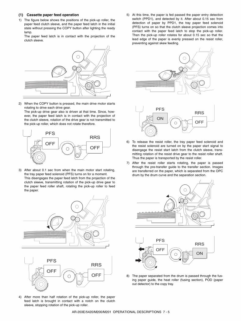
(1) Cassette paper feed operation1) The figure below shows the positions of the pick-up roller, the
paper feed clutch sleeve, and the paper feed latch in the initialstate without pressing the COPY button after lighting the readylamp.The paper feed latch is in contact with the projection of theclutch sleeve.
2) When the COPY button is pressed, the main drive motor startsrotating to drive each drive gear.The pick-up drive gear also is driven at that time. Since, how-ever, the paper feed latch is in contact with the projection ofthe clutch sleeve, rotation of the drive gear is not transmitted tothe pick-up roller, which does not rotate therefore.
3) After about 0.1 sec from when the main motor start rotating,the tray paper feed solenoid (PFS) turns on for a moment.This disengages the paper feed latch from the projection of theclutch sleeve, transmitting rotation of the pick-up drive gear tothe paper feed roller shaft, rotating the pick-up roller to feedthe paper.
4) After more than half rotation of the pick-up roller, the paperfeed latch is brought in contact with a notch on the clutchsleeve, stopping rotation of the pick-up roller.
5) At this time, the paper is fed passed the paper entry detectionswitch (PPD1), and detected by it. After about 0.15 sec fromdetection of paper by PPD1, the tray paper feed solenoid(PFS) turns on so that the clutch sleeve projection comes intocontact with the paper feed latch to stop the pick-up roller.Then the pick-up roller rotates for about 0.15 sec so that thelead edge of the paper is evenly pressed on the resist roller,preventing against skew feeding.
6) To release the resist roller, the tray paper feed solenoid andthe resist solenoid are turned on by the paper start signal todisengage the resist start latch from the clutch sleeve, trans-mitting rotation of the resist drive gear to the resist roller shaft.Thus the paper is transported by the resist roller.
7) After the resist roller starts rotating, the paper is passedthrough the pre-transfer guide to the transfer section. Imagesare transferred on the paper, which is separated from the OPCdrum by the drum curve and the separation section.
8) The paper separated from the drum is passed through the fus-ing paper guide, the heat roller (fusing section), POD (paperout detector) to the copy tray.
OFF
PFS
OFF
RRS
OFF
PFS
OFF
RRS
ON
PFS
OFF
RRS
OFF
PFS
ON
RRS
AR-203E/5420/M200/M201 OPERATIONAL DESCRIPTIONS 7 - 5
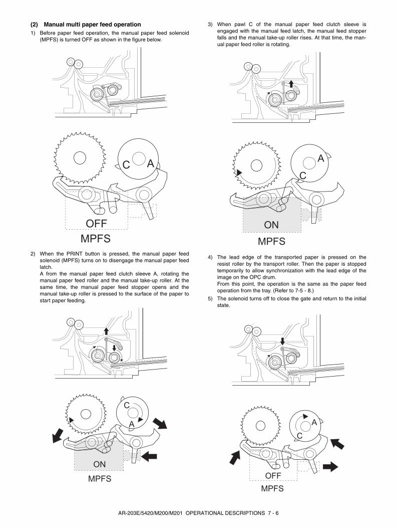
(2) Manual multi paper feed operation1) Before paper feed operation, the manual paper feed solenoid
(MPFS) is turned OFF as shown in the figure below.
2) When the PRINT button is pressed, the manual paper feedsolenoid (MPFS) turns on to disengage the manual paper feedlatch.A from the manual paper feed clutch sleeve A, rotating themanual paper feed roller and the manual take-up roller. At thesame time, the manual paper feed stopper opens and themanual take-up roller is pressed to the surface of the paper tostart paper feeding.
3) When pawl C of the manual paper feed clutch sleeve isengaged with the manual feed latch, the manual feed stopperfalls and the manual take-up roller rises. At that time, the man-ual paper feed roller is rotating.
4) The lead edge of the transported paper is pressed on theresist roller by the transport roller. Then the paper is stoppedtemporarily to allow synchronization with the lead edge of theimage on the OPC drum.From this point, the operation is the same as the paper feedoperation from the tray. (Refer to 7-5 - 8.)
5) The solenoid turns off to close the gate and return to the initialstate.
OFMPFS
F
C A
ON
MPFS
A
C
ONMPFS
A
C
OFMPFS
F
AC
AR-203E/5420/M200/M201 OPERATIONAL DESCRIPTIONS 7 - 6

(3) Conditions of occurrence of paper misfeed
a. When the power is turned on:PPD or POD is ON when the power is turned on.
b. Copy operation
6. D-D (Duplex to Duplex) mode paper/document transport (Duplex model) (AR-M201 only)
A. Initial stateSet duplex documents on the document tray.
Set paper on the cassette. (In the duplex mode, the manual feedtray cannot be selected.)
B. Front copyDocument transport:
The document feed roller feeds the document from the paper feedroller to the PS roller.
• The document is exposed in the exposure section, and trans-ported to the document exit section by the lower transport rollerand the paper exit roller.
• The document is transported to the paper exit tray. (However, it isnot discharged completely.)
• The document is stopped once, and then switchback operation isperformed. (To the back copy)
Paper transport:
The paper is passed through the paper feed roller and the PS roller,and the images on the front surface are transferred.
• The paper is passed through the fusing section and the lowerside of the gate section to the paper exit tray side. (However, it isnot discharged completely.)
• The paper is stopped once, and switchback operation is per-formed. (To the back copy)
C. Back copyDocument transport:
By switchback operation, the document is sent through the uppertransport roller and the PS roller to the exposure section, where theback surface of the document is exposed.
• The document is sent to the document exit section by the lowertransport roller and the paper exit roller.
• The document is sent to the intermediate tray. (However, it is notdischarged completely.)
• The document is stopped once, and switchback operation is per-formed.
• The document is sent through the upper transport roller and thePS roller and the exposure section (without being exposed) to thedocument exit section.
• The document is discharged to the document exit tray.
Paper transport:
Switchback operation is performed.
• The paper is sent through the upper side of the gate section andthe duplex transport section and the PS roller, and the images onthe back surface are transferred.
• The paper is sent through the fusing section and discharged tothe paper exit tray.
a PPD1 jam PPD1 does not turn off within 4 sec after turning on the resist roller.
b PPD2 jam PPD2 is off immediately after turning on the resist roller.
PPD2 does not turn off within 1.2 sec after turning off the resist roller.
c POD jam POD does not turn on within 2.9 sec after turning on the resist roller.
POD does not turn off within 1.5 sec - 2.7 sec after turning off PPD2.
AR-203E/5420/M200/M201 OPERATIONAL DESCRIPTIONS 7 - 7
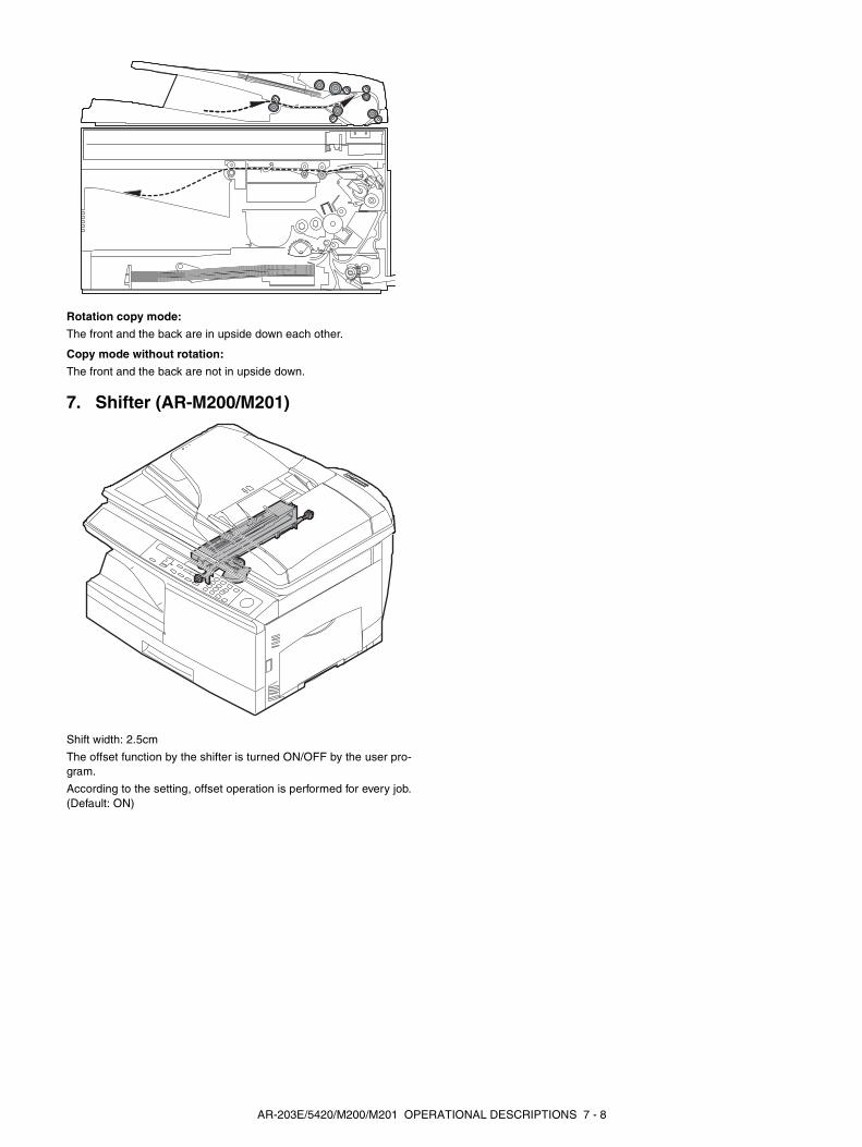
Rotation copy mode:
The front and the back are in upside down each other.
Copy mode without rotation:
The front and the back are not in upside down.
7. Shifter (AR-M200/M201)
Shift width: 2.5cm
The offset function by the shifter is turned ON/OFF by the user pro-gram.
According to the setting, offset operation is performed for every job.(Default: ON)
AR-203E/5420/M200/M201 OPERATIONAL DESCRIPTIONS 7 - 8

[8] DISASSEMBLY AND ASSEMBLY
The disassembly and assembly procedures are described for thefollowing sections:
1. High voltage section
2. Operation panel section
3. Optical section
4. Fusing section
5. Tray paper feed/transport section
6. Manual paper feed section
7. Rear frame section
8. Power section
9. DV unit section
10. Duplex motor section (AR-M201 only)
11. Reverse roller section (AR-M201 only)
1. High voltage sectionA. List
B. Drum replacement1) Remove the drum cover. (4 Lock Tabs)
2) Remove the drum fixing plate and the photoconductor drum.
(Note) Dispose the drum fixing plate which was removed.
3) Check the cleaning blade and the red felt for no damage.
• If there is any damage, execute all procedures from item 5)and later.
• If there is no damage, execute the procedure of item 12).
4) Remove the main charger.(When uneven charging occurs, clean the screen grid and thesawteeth with an air blower.)
5) Remove the cleaning blade.
Note: Dispose the cleaning blade which was removed. If a cleaning error occurs, replace the cleaning blade.(Recommendable replacement cycle: Every 25K)
Before disassembly, be sure to disconnect the power cord for safety.1. Do not disconnect or connect the connector and the
harness during the machine is powered. Especially be careful not to disconnect or connect the harness between the MCU PWB and the LSU (MCU PWB: CN119) during the machine is powered. (If it is disconnected or connected during the machine is powered, the IC inside the LSU will be destroyed.)
2. To disconnect the harness after turning on the power, be sure to turn off the power and wait for at least 10 sec before disconnection. (Note that a voltage still remains immediately after turning off the power.)
No. Part name Ref.1 Drum2 Transfer charger unit3 Charger wire
(2)
(3)
LO CK
AR-203E/5420/M200/M201 DISASSEMBLY AND ASSEMBLY 8 - 1

6) Clean the cleaning section and the waste toner pipe to removewaste toner completely with a vacuum cleaner.
7) Remove the felt and duplex tape completely.
Note: Be careful not to scratch or bend the sub blade.
8) Attach the cleaning blade.
Securely insert the plate section of the cleaning blade into theunit and fix it with a screw.
Do not touch the cleaning blade rubber with your hand.
When attaching the cleaning blade, press the cleaning bladein the arrow direction and attach.
Attach the cleaning blade, press the molt on the process framewith a screwdriver (–), and push it in the clearance between theprocess frame and the cleaning blade.
• Machine F side
• Machine R side
Normal state of the molt
• Machine F side
• Machine R side
9) Attach the moquettes.
Attach the mocket with slightly pressing section A of the clean-ing blade.
Do not touch the tip of the cleaning blade.
Do not put the mocket under the cleaning blade.
Do not put the mocket on the sub blade.
Do not press the sub blade with the mocket.
If the moquette F/R is deformed or damaged, replace it. (Recommendable replacement cycle: Every 25K)
0 – 0.3 mm 0 – 0.3 mm
0 – 0.5 mm0 – 0.5 mm
0.2
– 0.
5 m
m
0.2
– 0.
5 m
m
Cleaning blade
Cleaning blade
Moquette R
Sub blade
Sub blade
Moquette F
Moquette RMoquette F
∗ ∗
∗: Check while pressing the blade.
Be careful not to allow the moquette to cover the sub blade.
Example of NG
AR-203E/5420/M200/M201 DISASSEMBLY AND ASSEMBLY 8 - 2
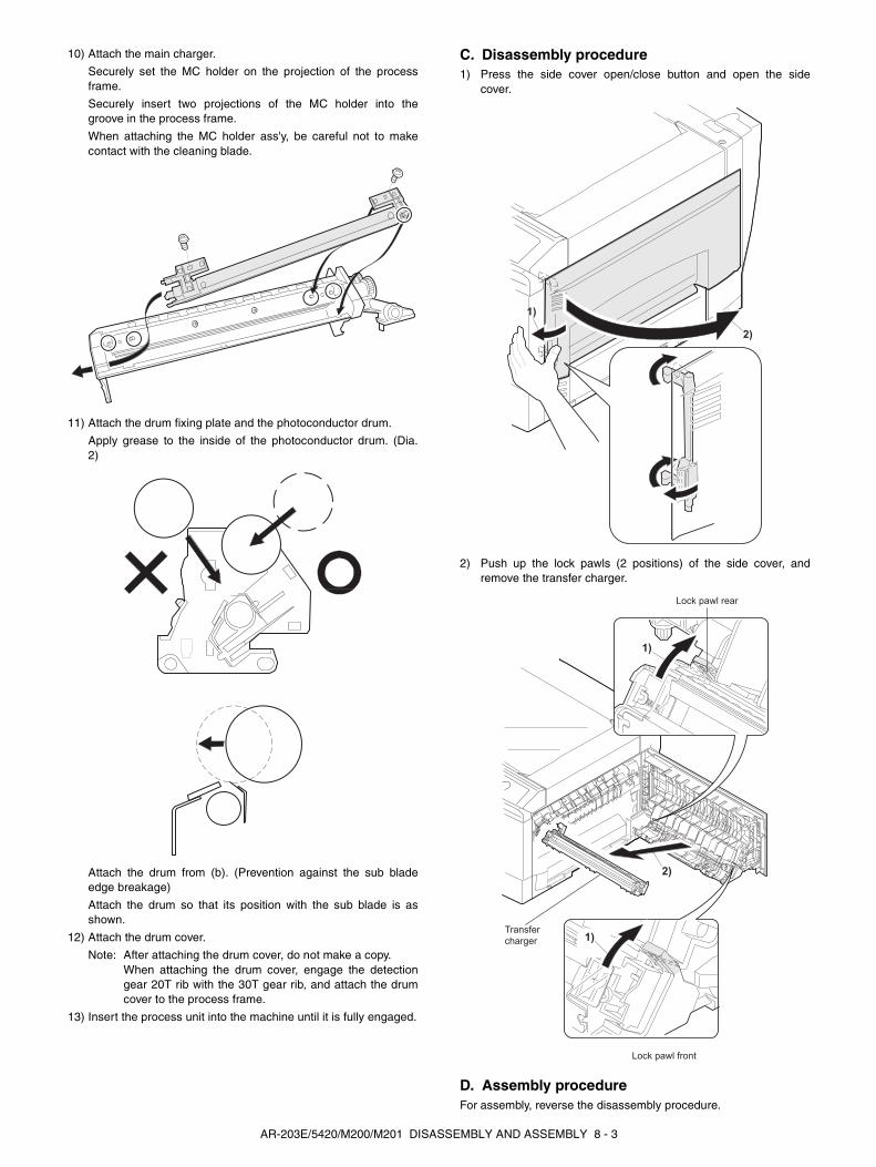
10) Attach the main charger.
Securely set the MC holder on the projection of the processframe.
Securely insert two projections of the MC holder into thegroove in the process frame.
When attaching the MC holder ass'y, be careful not to makecontact with the cleaning blade.
11) Attach the drum fixing plate and the photoconductor drum.
Apply grease to the inside of the photoconductor drum. (Dia.2)
Attach the drum from (b). (Prevention against the sub bladeedge breakage)
Attach the drum so that its position with the sub blade is asshown.
12) Attach the drum cover.
Note: After attaching the drum cover, do not make a copy. When attaching the drum cover, engage the detectiongear 20T rib with the 30T gear rib, and attach the drumcover to the process frame.
13) Insert the process unit into the machine until it is fully engaged.
C. Disassembly procedure1) Press the side cover open/close button and open the side
cover.
2) Push up the lock pawls (2 positions) of the side cover, andremove the transfer charger.
D. Assembly procedureFor assembly, reverse the disassembly procedure.
1)
2)
2)
1)
1)Transfercharger
Lock pawl rear
Lock pawl front
AR-203E/5420/M200/M201 DISASSEMBLY AND ASSEMBLY 8 - 3
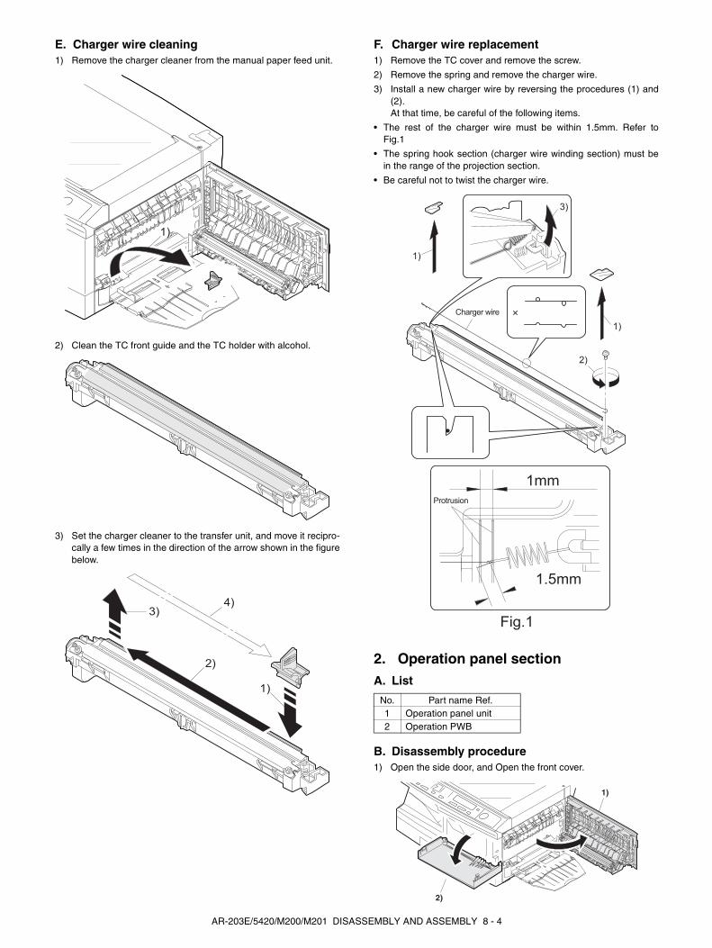
E. Charger wire cleaning1) Remove the charger cleaner from the manual paper feed unit.
2) Clean the TC front guide and the TC holder with alcohol.
3) Set the charger cleaner to the transfer unit, and move it recipro-cally a few times in the direction of the arrow shown in the figurebelow.
F. Charger wire replacement1) Remove the TC cover and remove the screw.
2) Remove the spring and remove the charger wire.
3) Install a new charger wire by reversing the procedures (1) and(2).At that time, be careful of the following items.
• The rest of the charger wire must be within 1.5mm. Refer toFig.1
• The spring hook section (charger wire winding section) must bein the range of the projection section.
• Be careful not to twist the charger wire.
2. Operation panel sectionA. List
B. Disassembly procedure1) Open the side door, and Open the front cover.
1)
1)
2)
3)4)
No. Part name Ref.1 Operation panel unit2 Operation PWB
1mm
1.5mm
Fig.1
1)
1)
2)
3)
Charger wire
Protrusion
1)
2)
AR-203E/5420/M200/M201 DISASSEMBLY AND ASSEMBLY 8 - 4

2) Remove the screws (4 pcs.), the harness, and the operationpanel unit.
3) Remove four screws, and remove the operation cabinet.
4) Remove four screws, and remove the operation PWB.
(AR-203E/5420)
(AR-M200/M201)
C. Assembly procedureFor assembly, reverse the disassembly procedure
3. Optical sectionA. List
B. Disassembly procedure1) Remove four screws, and remove the rear cabinet and the rear
cabinet cover.
1)
1)
1)
2)
1)
1)
1)1)
1)2)
3)3)
3)
3)3)
3)
3) 3)
4)
NO. Part name Ref.1 Copy lamp unit2 Copy lamp3 Lens unit
1)
3)
2)
4)
2)
5)
5)
5)
5)
1)
1)
2)
2)
1)
AR-203E/5420/M200/M201 DISASSEMBLY AND ASSEMBLY 8 - 5
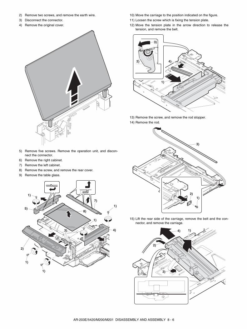
2) Remove two screws, and remove the earth wire.
3) Disconnect the connector.
4) Remove the original cover.
5) Remove five screws. Remove the operation unit, and discon-nect the connector.
6) Remove the right cabinet.
7) Remove the left cabinet.
8) Remove the screw, and remove the rear cover.
9) Remove the table glass.
10) Move the carriage to the position indicated on the figure.
11) Loosen the screw which is fixing the tension plate.
12) Move the tension plate in the arrow direction to release thetension, and remove the belt.
13) Remove the screw, and remove the rod stopper.
14) Remove the rod.
15) Lift the rear side of the carriage, remove the belt and the con-nector, and remove the carriage.
2)
4)
5)
7)
8)
1)
1)
1)
3)
1)
1)
1)
2) 4)
3)
1)2)
3)
1)
2)
4)
3)
AR-203E/5420/M200/M201 DISASSEMBLY AND ASSEMBLY 8 - 6

C. Assembly procedureCCD core
1) Insert the CCD-MCU harness into the CCD PWB of the car-riage unit.
2) Attach the CCD-MCU harness to the duplex tape on the backsurface of the carriage unit. Clean and remove oil and dirt fromthe attachment surface.
3) Pass the CCD-MCU harness through the square hole in thebase plate.
4) Attach the CCD-MCU harness to the base plate with duplextape.
5) Attach two cable fixing sheets to fix the CCD-MCU harness tothe base plate.
6) Pass the core through the CCD-MCU harness and fix the core.
7) Insert the CCD-MCU harness into the MCU PWB.
4. Fusing sectionA. List
B. Disassembly procedure1) Remove the connectors (3 pcs.) of the rear cabinet.
2) Open the side cover, remove two screws, and remove the fus-ing unit.
3) Cut the binding band, remove the screw, and remove the ther-mistor.
Note: Attach the FCC to the base plate securely with duplex tape to prevent against coming loose.
Note: Attach the FCC to fit with the marking line. Marking line.
No. Part name Ref.1 Thermistor2 PPD2 sensor3 Heater lamp4 Pressure roller5 Heat roller
1)
2)3)
2)
1)
2)
3)Thermistor
AR-203E/5420/M200/M201 DISASSEMBLY AND ASSEMBLY 8 - 7

4) Remove the screw and remove the U-turn guide.
Pressure roller section disassembly
5) Remove the three screws, remove the fusing cover lower onthe right side, and open the heat roller section.
6) Remove the screw and remove the PPD2 sensor.
7) Remove the plate spring on the right and remove the heaterlamp.
8) Remove the spring, and remove the upper separation pawls (3pcs.).
9) Remove the E-ring and remove the reverse gate.
1)
2)
1)
5)
5)
6)
6)
4)3)2)
1)
2)PPD2 sensor
1)
2)
Heater lamp
3)
1)
2)
2)
1)
3)
AR-203E/5420/M200/M201 DISASSEMBLY AND ASSEMBLY 8 - 8
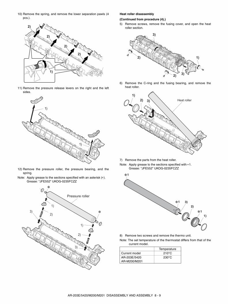
10) Remove the spring, and remove the lower separation pawls (4pcs.).
11) Remove the pressure release levers on the right and the leftsides.
12) Remove the pressure roller, the pressure bearing, and thespring.
Note: Apply grease to the sections specified with an asterisk (∗).Grease: "JFE552" UKOG-0235FCZZ
Heat roller disassembly
(Continued from procedure (4).)
5) Remove screws, remove the fusing cover, and open the heatroller section.
6) Remove the C-ring and the fusing bearing, and remove theheat roller.
7) Remove the parts from the heat roller.
Note: Apply grease to the sections specified with ∗1.Grease: "JFE552" UKOG-0235FCZZ
8) Remove two screws and remove the thermo unit.
Note: The set temperature of the thermostat differs from that of thecurrent model.
2)
2)
2)
1)
2)
1)
1)
1)
2)
2)
1)
3)
3)
Pressure roller
TemperatureCurrent model 210°CAR-203E/5420AR-M200/M201
230°C
1)
2)
2)
3)
3)
1)2) 3) Heat roller
3)2)
1)
1
1
1
AR-203E/5420/M200/M201 DISASSEMBLY AND ASSEMBLY 8 - 9
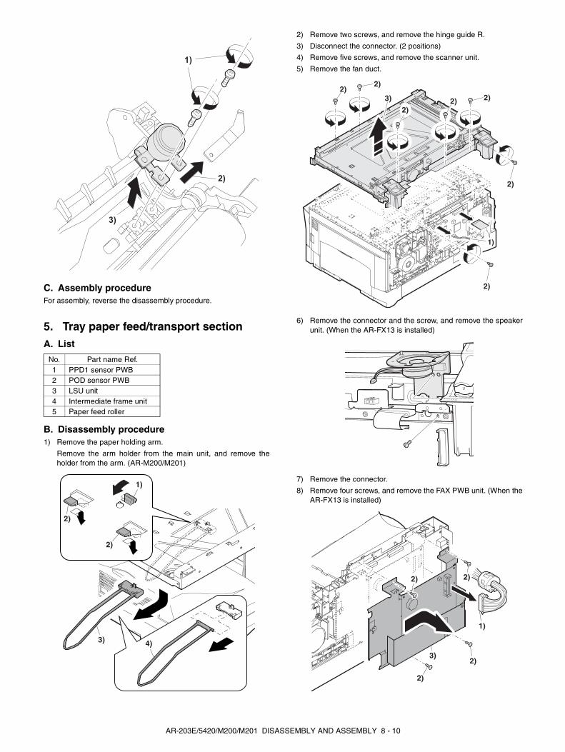
C. Assembly procedureFor assembly, reverse the disassembly procedure.
5. Tray paper feed/transport sectionA. List
B. Disassembly procedure1) Remove the paper holding arm.
Remove the arm holder from the main unit, and remove theholder from the arm. (AR-M200/M201)
2) Remove two screws, and remove the hinge guide R.
3) Disconnect the connector. (2 positions)
4) Remove five screws, and remove the scanner unit.
5) Remove the fan duct.
6) Remove the connector and the screw, and remove the speakerunit. (When the AR-FX13 is installed)
7) Remove the connector.
8) Remove four screws, and remove the FAX PWB unit. (When theAR-FX13 is installed)
No. Part name Ref.1 PPD1 sensor PWB2 POD sensor PWB3 LSU unit4 Intermediate frame unit5 Paper feed roller
1)
2)
3)
3)
1)
2)
2)
4)
2)
2)
1)
2)2)
2) 2)
2)
3)
2)
2)
3)
1)
2)
2)
AR-203E/5420/M200/M201 DISASSEMBLY AND ASSEMBLY 8 - 10

9) Remove each connector and four screws, and remove the MCUPWB. (The shape of the MCU PWB differs depending on themodel.)
10) Remove the PWB insulation mylar and remove the paper trans-port detection sensor (POD).
11) Remove two springs and open the intermediate frame unit. (AR-203E/5420)
12) Remove the screw, and open the upper paper guide. (AR-M200/M201)
13) Remove the roller, and remove the belt. (AR-M200/M201)
1)
1)1)
1)
2)
2)
3)
2)
1)
1)
2)
1)
1)
2)
1)1)
2)
1)
2)
AR-203E/5420/M200/M201 DISASSEMBLY AND ASSEMBLY 8 - 11

14) Remove the pulleys on the both sides and remove the paperexit roller. (AR-203E/5420)
15) Disengage the pawl, and remove the roller knob.
16) Disengage the pawl, and shift the pulley and the bearing.
17) Remove the paper exit roller, and remove the belt, the pulley,and the bearing.
18) Remove the harness guide.
19) Remove two screws and remove the toner motor.
20) Remove three screws, and remove the DUP motor unit and thebelt. (AR-M201)
4)
2)
1)3)
1)
2)3)
4)
1)2)
1)
2)
1)
1)
2) 3)
AR-203E/5420/M200/M201 DISASSEMBLY AND ASSEMBLY 8 - 12
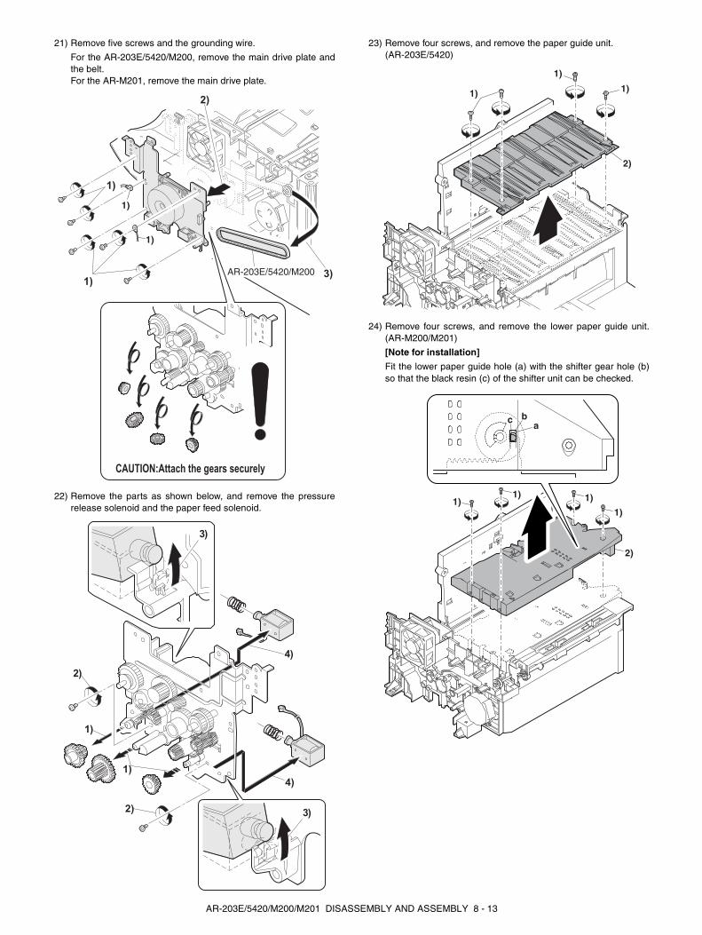
21) Remove five screws and the grounding wire.
For the AR-203E/5420/M200, remove the main drive plate andthe belt.For the AR-M201, remove the main drive plate.
22) Remove the parts as shown below, and remove the pressurerelease solenoid and the paper feed solenoid.
23) Remove four screws, and remove the paper guide unit. (AR-203E/5420)
24) Remove four screws, and remove the lower paper guide unit.(AR-M200/M201)
[Note for installation]
Fit the lower paper guide hole (a) with the shifter gear hole (b)so that the black resin (c) of the shifter unit can be checked.
1)
1)
3)
2)
1)
CAUTION:Attach the gears securely
1)
AL-2030 onlyAL-2030 onlyAR-203E/5420/M200
3)
3)
1)
1)
2)
2)
4)
4)
2)
1)
1)
1)
1)
1)1)1)
2)
abc
AR-203E/5420/M200/M201 DISASSEMBLY AND ASSEMBLY 8 - 13

25) Put the lower paper guide unit upside down, remove twoscrews, and remove the shifter motor. (AR-M200/M201)
26) Remove the screw, and remove the grounding plate and thegear. (AR-M200/M201)
27) Remove the E-ring, the gear, and the bearing, and remove theshifter roller. (AR-M200/M201)
28) Disengage the pawl, and remove the pulley.
29) Shift and remove the shifter unit. (AR-M200/M201)
30) Remove four screws, and remove the LSU unit.
[Note for assembling the LSU]
When installing the LSU, turn the LSU clockwise and fix withscrews in order to provide an attachment backlash in the properdirection.
Observe the following sequence of fixing screws.
1)
2)
1)
2)
3)
1)
2)
3)
3)
4)
1)
1)
1)
2)
AR-203E/5420/M200/M201 DISASSEMBLY AND ASSEMBLY 8 - 14

31) Remove the screw, slide the left cabinet to the left to detach it.
Remove each pawl, and remove the paper exit tray.
32) Remove two screws and remove the fusing connector.
33) Remove five screws and the connector, and lift the intermediateframe unit to remove.
34) Remove the screw and the E-ring, and remove the PS semi-cir-cular earth plate and the PS roller unit.
35) Remove the E-ring and remove the spring clutch from the PSroller unit.
36) Remove three screws and remove the TC front paper guide.
5)
1)2)
3)
4)
2)
2)
3)
4)
1)
5)
4)
4)
1)
2)
3)
PS roller unit
PS semi-circulerearth plate
5)
4)
4)
1)
2)
3)
PS semi-circularearth plate
Use grease of Floil FG40H only to apply to this section.
1)
2)
AR-203E/5420/M200/M201 DISASSEMBLY AND ASSEMBLY 8 - 15
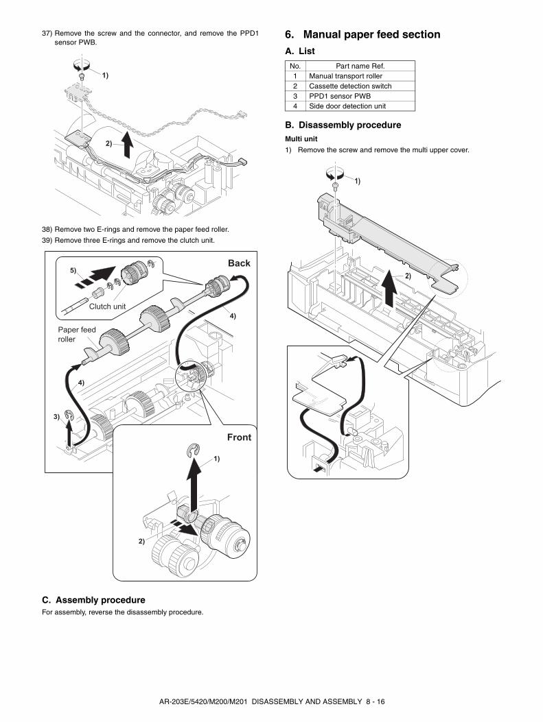
37) Remove the screw and the connector, and remove the PPD1sensor PWB.
38) Remove two E-rings and remove the paper feed roller.
39) Remove three E-rings and remove the clutch unit.
C. Assembly procedureFor assembly, reverse the disassembly procedure.
6. Manual paper feed sectionA. List
B. Disassembly procedureMulti unit
1) Remove the screw and remove the multi upper cover.
1)
2)
4)
5)
1)
2)
3)
4)
Back
Front
Clutch unit
Paper feedroller
No. Part name Ref.1 Manual transport roller2 Cassette detection switch3 PPD1 sensor PWB4 Side door detection unit
2)
1)
AR-203E/5420/M200/M201 DISASSEMBLY AND ASSEMBLY 8 - 16
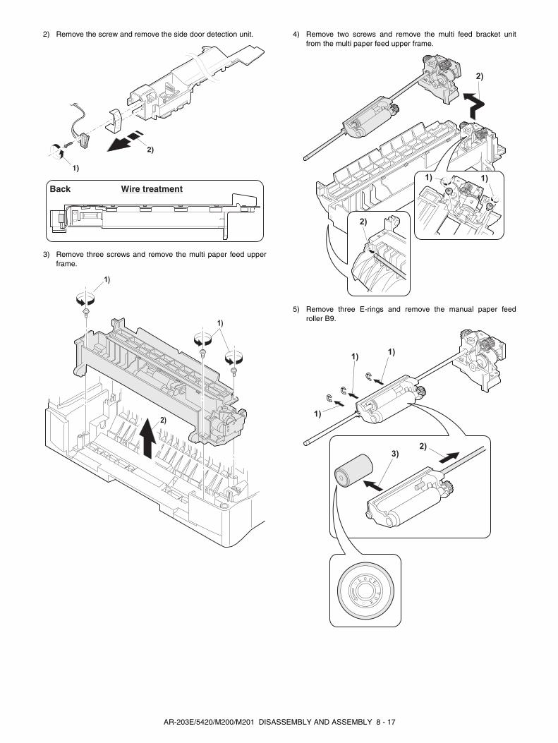
2) Remove the screw and remove the side door detection unit.
3) Remove three screws and remove the multi paper feed upperframe.
4) Remove two screws and remove the multi feed bracket unitfrom the multi paper feed upper frame.
5) Remove three E-rings and remove the manual paper feedroller B9.
1)
2)
Back Wire treatment
1)
2)
1)
2)
2)
1) 1)
2)
1) 1)
1)
3)
L O C K
TO
K
AR-203E/5420/M200/M201 DISASSEMBLY AND ASSEMBLY 8 - 17
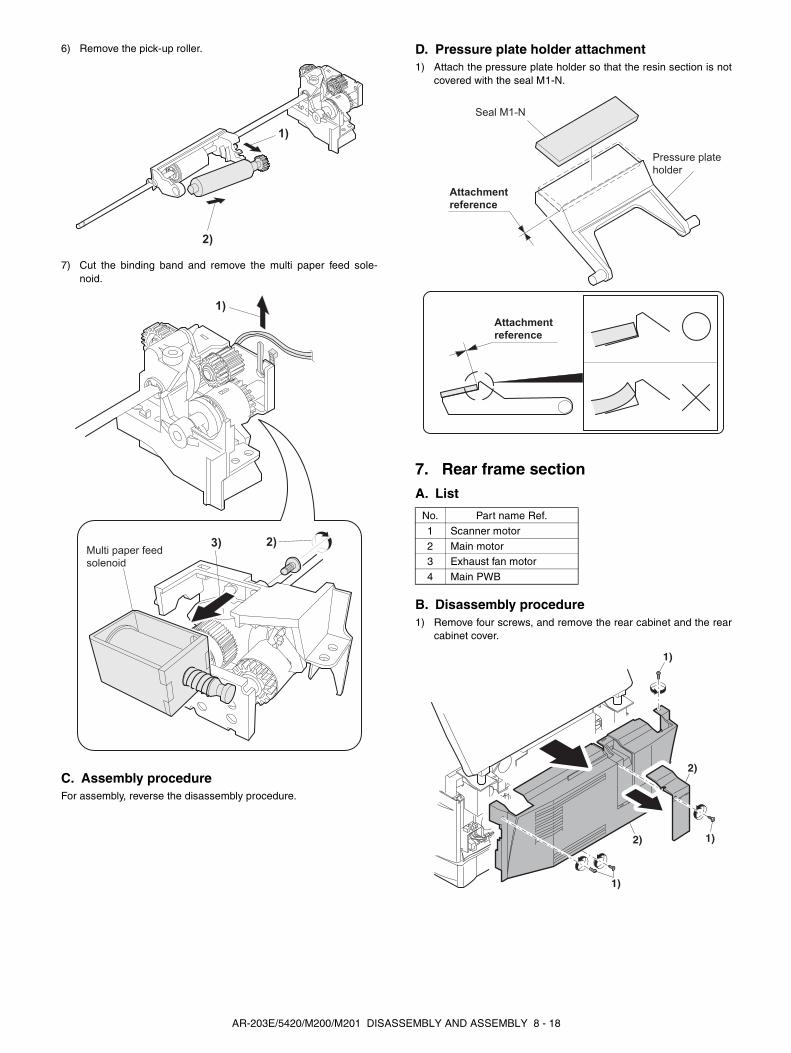
6) Remove the pick-up roller.
7) Cut the binding band and remove the multi paper feed sole-noid.
C. Assembly procedureFor assembly, reverse the disassembly procedure.
D. Pressure plate holder attachment1) Attach the pressure plate holder so that the resin section is not
covered with the seal M1-N.
7. Rear frame sectionA. List
B. Disassembly procedure1) Remove four screws, and remove the rear cabinet and the rear
cabinet cover.
2)
1)
1)
2)3)Multi paper feedsolenoid
No. Part name Ref.
1 Scanner motor
2 Main motor3 Exhaust fan motor
4 Main PWB
Pressure plateholder
Seal M1-N
Attachmentreference
Attachmentreference
1)
1)
2)
2)
1)
AR-203E/5420/M200/M201 DISASSEMBLY AND ASSEMBLY 8 - 18
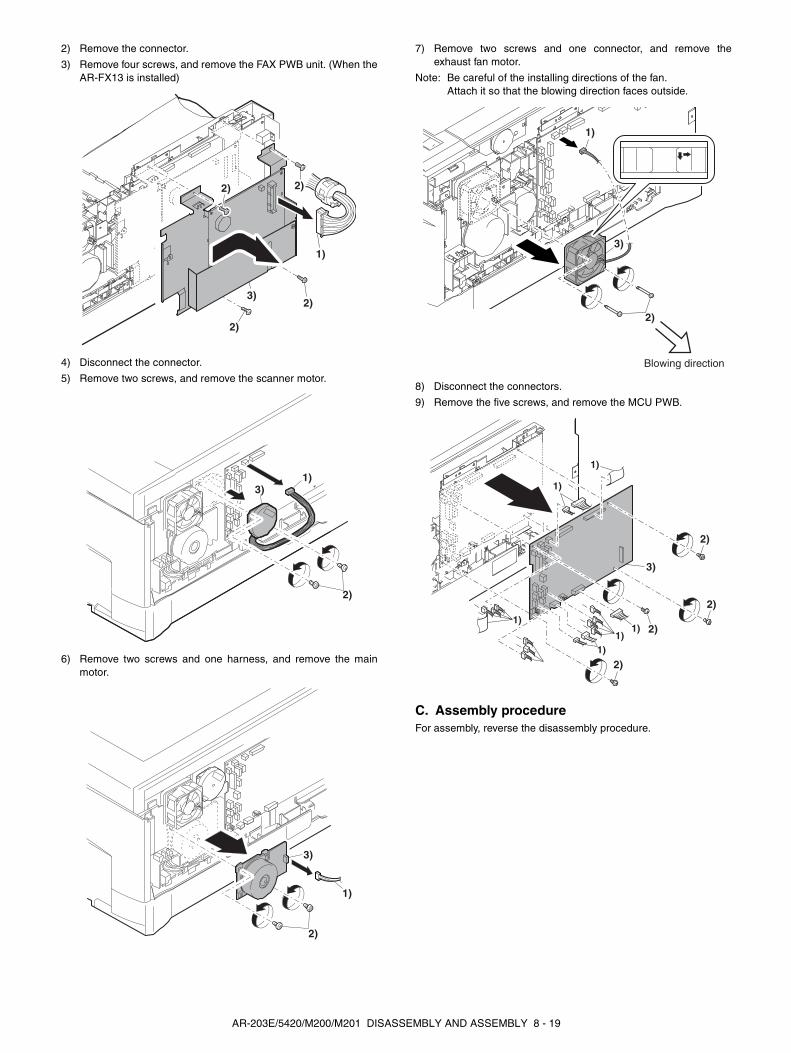
2) Remove the connector.
3) Remove four screws, and remove the FAX PWB unit. (When theAR-FX13 is installed)
4) Disconnect the connector.
5) Remove two screws, and remove the scanner motor.
6) Remove two screws and one harness, and remove the mainmotor.
7) Remove two screws and one connector, and remove theexhaust fan motor.
Note: Be careful of the installing directions of the fan.Attach it so that the blowing direction faces outside.
8) Disconnect the connectors.
9) Remove the five screws, and remove the MCU PWB.
C. Assembly procedureFor assembly, reverse the disassembly procedure.
2)
2)
3)
1)
2)
2)
1)
2)
3)
1)
2)
3)
1)
2)
3)
Blowing direction
2)
3)
2)
2)
2)1)
1)
1)1)
1)
1)
AR-203E/5420/M200/M201 DISASSEMBLY AND ASSEMBLY 8 - 19
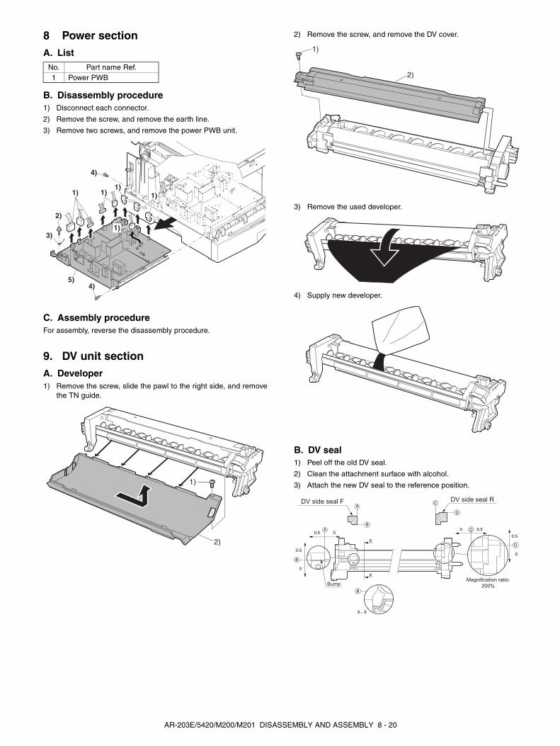
8 Power sectionA. List
B. Disassembly procedure1) Disconnect each connector.
2) Remove the screw, and remove the earth line.
3) Remove two screws, and remove the power PWB unit.
C. Assembly procedureFor assembly, reverse the disassembly procedure.
9. DV unit sectionA. Developer1) Remove the screw, slide the pawl to the right side, and remove
the TN guide.
2) Remove the screw, and remove the DV cover.
3) Remove the used developer.
4) Supply new developer.
B. DV seal1) Peel off the old DV seal.
2) Clean the attachment surface with alcohol.
3) Attach the new DV seal to the reference position.
No. Part name Ref.1 Power PWB
1) 1)1)
1)
2)
3)
4)
4)5)
1)
1)
2)
1)
2)
B
X - X
D
C
B
A
A
B
0
0
X
X
D
0
0.5
0.50.5
0.50
DV side seal F DV side seal R
BumpMagnification ratio:
200%
C
AR-203E/5420/M200/M201 DISASSEMBLY AND ASSEMBLY 8 - 20

C. DV blade1) Peel off the old DV blade.
2) Clean the attachment surface with alcohol.
3) Attach the new DV blade to the reference position.
D. DV doctor1) Remove the screw, and remove the DV doctor.
* Clean the edge (A) section.
Note for installation
1) Insert the DG check gauge as shown in the figure.
2) After checking, install the doctor gap and fix it with a screw.
* Apply screw lock to the screw tightening section as shown in thefigure below.
E. DV sensor1) Remove the Mylar.
2) Remove the screw, and remove the DV sensor.
* Clean the sensor (A) section.
10. Duplex motor section (AR-M201 only)A. List
B. Disassembly procedure1) Remove the rear cabinet.
2) Remove two screws.
3) Remove the Duplex motor cover.
4) Remove the Duplex motor.
Note: When reassembling, be sure to engage the Duplex motorgear with the belt on the main body side.
C. Assembly procedureFor assembly, reverse the disassembly procedure.
B
A
B
A
DV-BOX AS
0.5 0DV blade IC
1)
2)A
1)
F/Rsection
Csection
REAR
MG-ROL
DG:1.550.15
DG:1.50.10
FRONT
20 2010 10
110
F C R
* After checking the DG,apply screw lock.
DG checkgauge
DG checkgauge
DG checkgauge
DG checkgauge
12
DG checkposition
No. Part name Ref.
1 Duplex motor
1)
2)
2)
A
3)
12
31
AR-203E/5420/M200/M201 DISASSEMBLY AND ASSEMBLY 8 - 21

11. Reverse roller section (AR-M201 only)A. List
B. Disassembly procedure1) Remove four screws.
2) Remove the spring, and the earth wire.
3) Remove the reverse unit.
4) Bend the reverse roller and remove it.
C. Assembly procedureFor assembly, reverse the disassembly procedure.
No. Part name Ref.
1 Reverse roller
1
2
3
1
AR-203E/5420/M200/M201 DISASSEMBLY AND ASSEMBLY 8 - 22

[9] ADJUSTMENTS
1. Optical sectionA. Copy magnification ratio adjustmentThe copy magnification ratio must be adjusted in the main scan-ning direction and in the sub scanning direction. To adjust, useSIM 48-1.
(1) OutlineThe main scanning (front/rear) direction magnification ratio adjust-ment is made automatically or manually.
Automatic adjustment: The width of the reference line marked onthe shading correction plate is scanned to perform the main scan-ning (front/rear) direction magnification ratio adjustment automati-cally.
Manual adjustment: The adjustment is made by [Copy quantity]keys (or [Numeric] keys for the AR-M200/M201) operations. (Ineither of the automatic and manual adjustments, the zoom data reg-ister set value is changed for adjustment.)
The magnification ratio in the sub scanning direction is adjusted bychanging the carriage (scanner) scanning speed.
(2) Main scanning direction magnification ratio adjustment
a. Cases when the adjustment is required
1) When the main PWB is replaced.
2) When the EEPROM in the main PWB is replaced.
3) When "U2" trouble occurs.
4) When repairing or replacing the optical section.
b. Necessary tools
• Screwdriver (+)
• Scale
c. Adjustment procedure
1) Set the scale vertically on the document table. (Use a longscale for precise adjustment.)
2) Set the copy magnification ratio to 100%.
3) Make a copy on A4 or 81/2" x 11" paper.
4) Measure the length of the copied scale image.
5) Calculate the main scanning direction magnification ratio. Main scanning direction magnification ratio
6) Check that the copy magnification ratio is within the specifiedrange. If it is not within the specified range, perform the follow-ing procedures.
7) Execute SIM 48-1 to select the main scanning direction copymagnification ratio adjustment mode.To select the adjustment mode, use the [Exposure mode selec-tor] key (or [ ] [ ] key for the AR-M200/M201).
In the case of the automatic adjustment, when the START switch ispressed, the mirror base unit moves to the white plate for shadingto scan the width of the reference line, calculating the correctionvalue and displaying and storing this value.
After execution of the automatic adjustment, go out from the simu-lation mode and make a copy to check the magnification ratio.
If the magnification ratio is not in the specified range (100 ± 1.0%),manually adjust as follows.
(AR-203E/5420)
(AR-M200/M201)
8) Enter the new set value of main scanning direction copy magni-fication ratio with the copy quantity key (or [Numeric] key for theAR-M200/M201), and press the [START] key.
9) Change the set value and repeat the adjustment until the ratio iswithin the specified range.When the set value is changed by 1, the magnification ratio ischanged by 0.1%.
(3) Sub scanning direction copy magnification ratio
a. Cases when the adjustment is required
1) When the scanner unit drive section is disassembled or the partis replaced.
2) When the main PWB is replaced.
3) When the EEPROM in the main PWB is replaced.
4) When "U2" trouble occurs.
b. Necessary tools
• Scale
=Copy image dimensions
X 100 (%)Original dimension
Adjustment mode Display lamp DefaultMain scanning direction magnification ratio
TEXT mode lamp 50
OC mode sub scan direction magnification ratio
PHOTO mode lamp 50
Adjustment modeDisplay
itemLED Default
Main scan direction magnification ratio
F-R PRINT mode lamp 50
OC mode sub scan direction magnification ratio
SCAN SCAN mode lamp 50
100 110 120 130 150140mm1/2mm
JAPAN
HARDENEDSTAINLESS
Shizuoka
100 110 120 130 150140mm1/2mm
JAPAN
HARDENEDSTAINLESS
Shizuoka
110
10 20
10 20
(When a 100mm scale is used as the original.)
Paper feeddirection
Reference Comparison point
Original (Scale)
Copy
AR-203E/5420/M200/M201 ADJUSTMENTS 9 - 1

c. Adjustment procedure
1) Set the scale on the document table as shown below. (Use along scale for precise adjustment.)
2) Set the copy magnification ratio to 100%.
3) Make a copy on A4 or 81/2" x 11" paper.
4) Measure the length of the copied scale image.
5) Calculate the sub scanning direction copy magnification ratiousing the formula below.
6) Check that the actual copy magnification ratio is within thespecified range. (100 ± 1.0%).If it is not within the specified range, perform the following pro-cedures.
7) Execute SIM 48-1 to select the sub scanning direction copymagnification ratio adjustment mode.To select the adjustment mode, use the [Exposure mode selec-tor] key (or [ ] [ ] key for the AR-M200/M201). (PHOTOlamp ON (or SCAN mode lamp ON for the AR-M200/M201))
8) Enter the new set value of sub scanning direction copy magnifi-cation ratio with the [Copy quantity] keys (or [Numeric] keys forthe AR-M200/M201), and press the [START] key.
Repeat procedures 1) - 8) until the sub scanning direction actualcopy magnification ratio in 100% copying is within the specifiedrange.
When the set value is changed by 1, the magnification ration ischanged by 0.1%.
B. Image position adjustmentThere are following eleven kinds of image position adjustments,which are made by laser control except for the image scan startposition adjustment. For the adjustments, SIM 50-01 and 50-10 areused.
(AR-203E/5420)
To select the adjustment mode with SIM 50-01, use the [Exposuremode selector] key.
The relationship between the adjustment modes and the lightinglamps are as shown in the table below.
: Supported for the installing model and skipped for non-install-ing mode.
To select the adjustment mode with SIM 50-10, use the [Exposuremode selector] key.
The relationship between the adjustment modes and the lightinglamps are as shown in the table below.
Machine with the multi manual paper feed unit
: Supported for the installing model and skipped for non-install-ing mode.
=Copy image dimensions
X 100 (%)Original dimension
100 110 120 130 150140mm1/2mm
JAPAN
HARDDENCDSTAINLESS
Shizuoka
100 110 120 130 150140mm1/2mm
JAPAN
HARDDENCDSTAINLESS
Shizuoka
110
10 20
10 20
Original (Scale)
Paper feeddirection
Reference Comparison point Copy
No. Mode SIM1 Print start position (Main cassette paper feed) 50-01
2 Print start position (2nd cassette paper feed) 50-01
3 Print start position (Manual paper feed) 50-01
4 Image lead edge void amount 50-01
5 Image scan start position 50-01
6 Image rear edge void amount (Cassette paper feed) 50-017 Image rear edge void amount (Manual paper feed) 50-01
8 Print center offset (Main cassette paper feed) 50-10
9 Print center offset (2nd cassette paper feed) 50-10
10 Print center offset (Manual paper feed) 50-10
11 2nd print center offset (Main cassette paper feed) 50-10
Adjustment mode Lamp ONPrint start position (Main cassette paper feed)
AE, main cassette lamp
Print start position (2nd cassette paper feed)
AE, 2nd cassette lamp
Print start position (Manual paper feed)
AE, manual feed lamp
Image lead edge void quantity TEXT lamp
Image scan start position PHOTO lamp
Image rear edge void quantity AE, TEXT, PHOTO lamp
Adjustment mode Lamp ON
Print center offset (Main cassette paper feed)
AE, main cassette lamp
Print center offset (2nd cassette) AE, 2nd cassette lamp
Print center offset (Manual paper feed)
AE, manual paper feed lamp
Second side center offset TEXT lamp
AR-203E/5420/M200/M201 ADJUSTMENTS 9 - 2

(AR-M200/M201)
To select the adjustment mode with SIM 50-01, use the [ ] [ ]key.
The relationship between the adjustment modes and the lightinglamps are as shown in the table below.
To select the adjustment mode with SIM 50-10, use the [ ] [ ]key.
The relationship between the adjustment modes and the lightinglamps are as shown in the table below.
(1) Lead edge adjustment1) Set a scale to the center of the paper lead edge guide as shown
below, and cover it with B4 or 8 1/2" x 14" paper.
2) Execute SIM 50-01
3) Set the print start position (AE lamp ON) (A), the lead edge voidamount (TEXT lamp ON) (B), and the scan start position(PHOTO lamp ON) (C) to 0, and make a copy of a scale at100%. (AR-203E/5420)
For the AR-M200/M201, the following LED’s are lighted:
• AE lamp/COPY mode lamp: (A)
• TEXT lamp/PRINT mode lamp: (B)
• PHOTO lamp/SCAN mode lamp: (C)
4) Measure the image loss amount (R mm) of the scale image.Set C = 10 X R (mm). (Example: Set the value of C to 30.)When the value of C is increased by 10, the image loss isdecreased by 1mm. (Default: 50)
5) Measure the distance (H mm) between the paper lead edgeand the image print start position.Set A = 10 X H (mm). (Example: Set the value of A to 50.)When the value of A is increased by 10, the image lead edge isshifted to the paper lead edge by 1mm. (Default: 50)
6) Set the lead edge void amount to B = 50 (2.5mm).When the value of B is increased by 10, the void amount isincreased by about 1mm. For 25 or less, however, the voidamount becomes zero. (Default: 50)
(2) Image rear edge void amount adjustment1) Set a scale to the rear edge section of A4 or 11" x 8 1/2" paper
size as shown in the figure below, and cover it with B4 or 8 1/2"x 14" paper.
2) Execute SIM 50-01 to select the image rear edge void amountadjustment mode.The set adjustment value is displayed on the copy quantity dis-play.
3) Make a copy and measure the void amount of image rear edge.
Adjustment mode Display item Lamp ONPrint start position (Main cassette paper feed)
TRAY1 COPY mode lampMain cassette lamp
(*) Print start position (2nd cassette paper feed)
TRAY2 COPY mode lamp2nd cassette lamp
Print start position (Manual paper feed)
MFT COPY mode lampManual paper feed lamp
Image lead edge void amount
DEN-A PRINT mode lampMain cassette lamp
Image scan start position RRC-A SCAN mode lampMain cassette lamp
Image rear edge void amount (Cassette paper feed)
DEN-B COPY mode lampPRINT mode lampSCAN mode lampMain cassette lamp
Image rear edge void amount (Manual paper feed)
RRC-B COPY mode lampPRINT mode lampManual paper feed lamp
Adjustment mode Display item Lamp ON
Print center offset (Main cassette paper feed)
TRAY1 COPY mode lampMain cassette lamp
Print center offset (2nd cassette paper feed)
TRAY2 COPY mode lamp2nd cassette lamp
Print center offset (Manual paper feed)
MFT COPY mode lampManual paper feed lamp
2nd print center offset (Main cassette paper feed)
SIDE2 PRINT mode lampMain cassette lamp
5mm
10mm
(Example)Distance between paper leadedge and image: H = 5mm
Image loss:R = 3mm
B4 or 8 1/2″ × 14″ paper
A4 size rear edge
Paper rear edge
Void amount (Standard value: 2 - 3mm)
Scale image
AR-203E/5420/M200/M201 ADJUSTMENTS 9 - 3
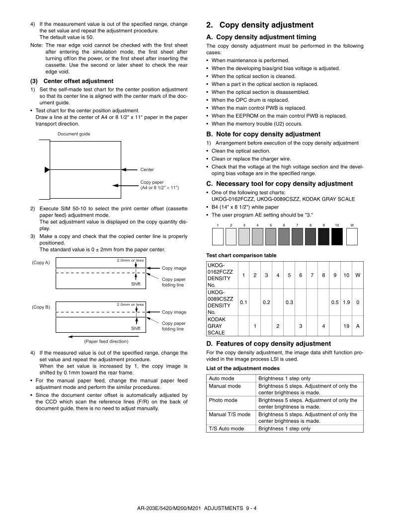
4) If the measurement value is out of the specified range, changethe set value and repeat the adjustment procedure.The default value is 50.
Note: The rear edge void cannot be checked with the first sheetafter entering the simulation mode, the first sheet afterturning off/on the power, or the first sheet after inserting thecassette. Use the second or later sheet to check the rearedge void.
(3) Center offset adjustment1) Set the self-made test chart for the center position adjustment
so that its center line is aligned with the center mark of the doc-ument guide.
• Test chart for the center position adjustment.Draw a line at the center of A4 or 8 1/2" x 11" paper in the papertransport direction.
2) Execute SIM 50-10 to select the print center offset (cassettepaper feed) adjustment mode.The set adjustment value is displayed on the copy quantity dis-play.
3) Make a copy and check that the copied center line is properlypositioned.The standard value is 0 ± 2mm from the paper center.
4) If the measured value is out of the specified range, change theset value and repeat the adjustment procedure.When the set value is increased by 1, the copy image isshifted by 0.1mm toward the rear frame.
• For the manual paper feed, change the manual paper feedadjustment mode and perform the similar procedures.
• Since the document center offset is automatically adjusted bythe CCD which scan the reference lines (F/R) on the back ofdocument guide, there is no need to adjust manually.
2. Copy density adjustmentA. Copy density adjustment timingThe copy density adjustment must be performed in the followingcases:
• When maintenance is performed.
• When the developing bias/grid bias voltage is adjusted.
• When the optical section is cleaned.
• When a part in the optical section is replaced.
• When the optical section is disassembled.
• When the OPC drum is replaced.
• When the main control PWB is replaced.
• When the EEPROM on the main control PWB is replaced.
• When the memory trouble (U2) occurs.
B. Note for copy density adjustment1) Arrangement before execution of the copy density adjustment
• Clean the optical section.
• Clean or replace the charger wire.
• Check that the voltage at the high voltage section and the devel-oping bias voltage are in the specified range.
C. Necessary tool for copy density adjustment• One of the following test charts:
UKOG-0162FCZZ, UKOG-0089CSZZ, KODAK GRAY SCALE
• B4 (14" x 8 1/2") white paper
• The user program AE setting should be "3."
Test chart comparison table
D. Features of copy density adjustmentFor the copy density adjustment, the image data shift function pro-vided in the image process LSI is used.
List of the adjustment modes
Document guide
Center
Copy paper(A4 or 8 1/2″ × 11″)
(Copy A)
(Copy B)
2.0mm or less
2.0mm or less
Copy image
Copy paperfolding line
Copy image
Copy paperfolding line
Shift
Shift
(Paper feed direction)
UKOG-0162FCZZDENSITYNo.
1 2 3 4 5 6 7 8 9 10 W
UKOG-0089CSZZDENSITYNo.
0.1 0.2 0.3 0.5 1.9 0
KODAKGRAYSCALE
1 2 3 4 19 A
Auto mode Brightness 1 step only
Manual mode Brightness 5 steps. Adjustment of only the center brightness is made.
Photo mode Brightness 5 steps. Adjustment of only the center brightness is made.
Manual T/S mode Brightness 5 steps. Adjustment of only the center brightness is made.
T/S Auto mode Brightness 1 step only
1 10 W2 3 4 5 6 7 8 9
AR-203E/5420/M200/M201 ADJUSTMENTS 9 - 4

E. Copy density adjustment procedureUse SIM 46-1 to set the copy density for each copy mode.
For selection of modes, use the [Exposure mode selector] key (or[ ] [ ] key for the AR-M200/M201).
(1) Test chart (UKOG-0162FCZZ) setting1) Place the test chart so that its edge is aligned with the A4 (Let-
ter) reference line on the document table. Then place a A4(14" x 8 1/2") white paper on the test chart and close the docu-ment cover.
(2) Perform the adjustment in each mode.1) Execute SIM 46-01 (300dpi). To adjust in 600dpi, execute SIM
46-02.
2) AR-203E/5420
Select the mode to be adjusted with the exposure mode selectkey. Set the exposure level to 3 for all adjustment. (Except forthe auto mode.)
2) AR-M200/M201
Select the mode to be adjusted with the exposure key. Set theexposure level to 3 (center) for all adjustment. (Except for theauto mode.)
3) Make a copy.Check the adjustment level (shown in the above table) of theexposure test chart (Sharp Gray Scale).
(When too bright): Decrease the value displayed on the copyquantity display.
(When too dark): Increase the value displayed on the copy quan-tity display.
∗ The value can be set in the range of 1 - 99.
3. High voltage adjustmentA. Main charger (Grid bias)Note:
• Use a digital multi meter with internal resistance of 10MΩ ormore measurement.
• After adjusting the grid LOW output, adjust the HIGH output. Donot reverse the sequence.
Procedures
1) Set the digital multi meter range to DC700V.
2) Set the positive side of the test rod to the connector CN11-3(GRID) of high voltage section of the power PWB and set thenegative side to the frame ground (power frame).
3) Execute SIM 8-2. (The main charger output is supplied for 30sec in the grid voltage HIGH output mode.)
4) Adjust the control volume (VRG1) so that the output voltage is580 ± 12V.
Adjustment mode
Exposure modedisplay lamp
Sharp gray chart adjustment level
Auto mode Auto lamp ON "3" is slightly copied.
Manual mode Manual lamp ON "3" is slightly copied.
Photo mode Photo lamp ON "3" is slightly copied.
Manual T/S mode
Manual lamp/Photo lamp ON "3" is slightly copied.
Auto T/S mode
Auto lamp/Photo lamp ON "3" is slightly copied.
Test chart
White paper
(1) (2)
Exposure mode select key/display lamp
[Exposure mode selector] key/display lamp
(1)
(2)
1 1 22 22 1 1 (2) Exposure key
(1) Exposure mode, level displayTEXT | | | | |
Adjustment mode
Display item
LEDSharp gray chart adjustment level
Auto mode AE COPY mode lamp "3" is slightly copied.
Text mode TEXT PRINT mode lamp "3" is slightly copied.
Photo mode PHOTO SCAN mode lamp "3" is slightly copied.
Text T/S mode TSTXT PRINT mode lampSCAN mode lamp
"3" is slightly copied.
Auto T/S mode TSAE COPY mode lampSCAN mode lamp
"3" is slightly copied.
Sharp Gray Scale adjustment level
Non toner save mode
Toner save mode
1 10 W2 3 4 5 6 7 8 9
Slightly copied.
Not copied.
1 10 W2 3 4 5 6 7 8 9
Slightly copied.
Not copied.
VRG1
AR-203E/5420/M200/M201 ADJUSTMENTS 9 - 5
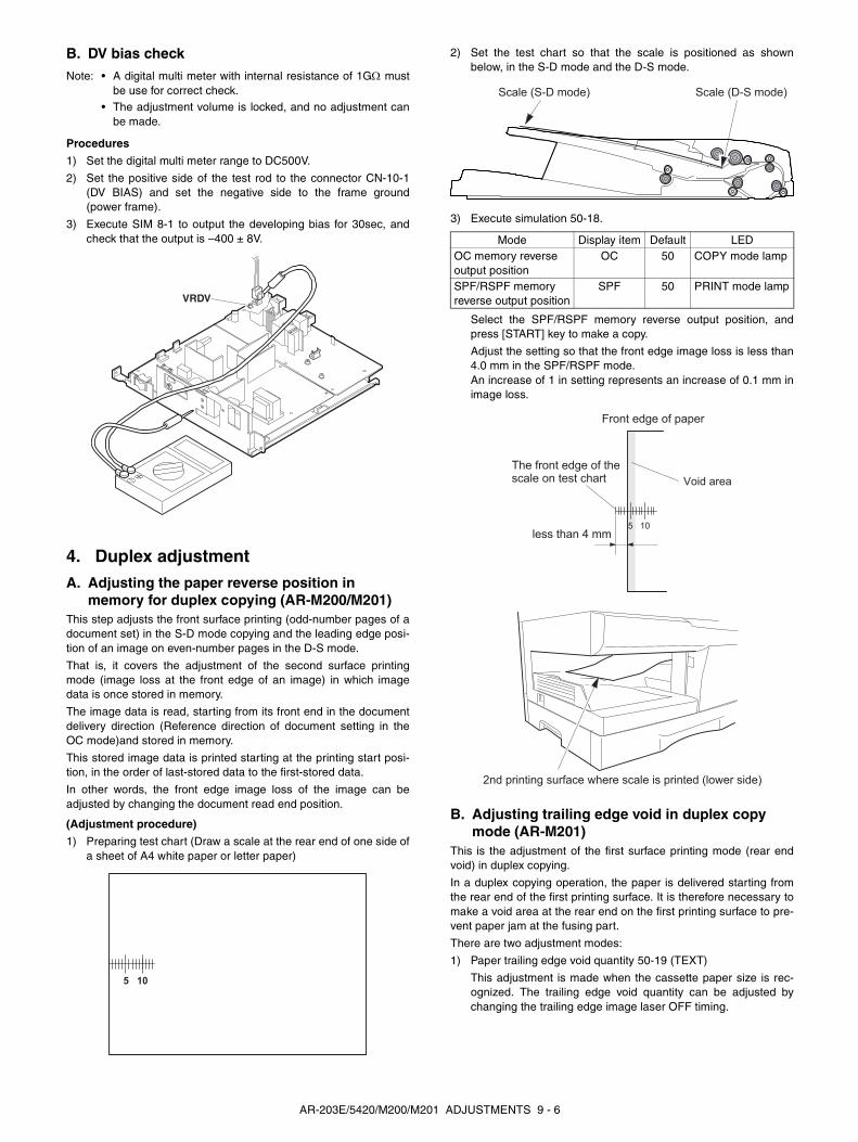
B. DV bias check
Procedures
1) Set the digital multi meter range to DC500V.
2) Set the positive side of the test rod to the connector CN-10-1(DV BIAS) and set the negative side to the frame ground(power frame).
3) Execute SIM 8-1 to output the developing bias for 30sec, andcheck that the output is –400 ± 8V.
4. Duplex adjustmentA. Adjusting the paper reverse position in
memory for duplex copying (AR-M200/M201)This step adjusts the front surface printing (odd-number pages of adocument set) in the S-D mode copying and the leading edge posi-tion of an image on even-number pages in the D-S mode.
That is, it covers the adjustment of the second surface printingmode (image loss at the front edge of an image) in which imagedata is once stored in memory.
The image data is read, starting from its front end in the documentdelivery direction (Reference direction of document setting in theOC mode)and stored in memory.
This stored image data is printed starting at the printing start posi-tion, in the order of last-stored data to the first-stored data.
In other words, the front edge image loss of the image can beadjusted by changing the document read end position.
(Adjustment procedure)
1) Preparing test chart (Draw a scale at the rear end of one side ofa sheet of A4 white paper or letter paper)
2) Set the test chart so that the scale is positioned as shownbelow, in the S-D mode and the D-S mode.
3) Execute simulation 50-18.
Select the SPF/RSPF memory reverse output position, andpress [START] key to make a copy.
Adjust the setting so that the front edge image loss is less than4.0 mm in the SPF/RSPF mode.An increase of 1 in setting represents an increase of 0.1 mm inimage loss.
B. Adjusting trailing edge void in duplex copy mode (AR-M201)
This is the adjustment of the first surface printing mode (rear endvoid) in duplex copying.
In a duplex copying operation, the paper is delivered starting fromthe rear end of the first printing surface. It is therefore necessary tomake a void area at the rear end on the first printing surface to pre-vent paper jam at the fusing part.
There are two adjustment modes:
1) Paper trailing edge void quantity 50-19 (TEXT)
This adjustment is made when the cassette paper size is rec-ognized. The trailing edge void quantity can be adjusted bychanging the trailing edge image laser OFF timing.
Note: • A digital multi meter with internal resistance of 1GΩ mustbe use for correct check.
• The adjustment volume is locked, and no adjustment canbe made.
VRDV
5 10
Mode Display item Default LEDOC memory reverse output position
OC 50 COPY mode lamp
SPF/RSPF memory reverse output position
SPF 50 PRINT mode lamp
Scale (S-D mode) Scale (D-S mode)
5 10
The front edge of thescale on test chart
Front edge of paper
Void area
less than 4 mm
2nd printing surface where scale is printed (lower side)
AR-203E/5420/M200/M201 ADJUSTMENTS 9 - 6

2) Print start position (Duplex back surface) (SPF/RSPF) 50-19(PHOTO)
The size (length) of a document read from the SPF/RSPF isdetected, the image at the trailing edge of the first printing sur-face is cut to make a void area. (The adjustment of void quantityat the time when the cassette paper size is not recognized.)
The paper void quantity should be first adjusted before the imagecut trailing edge void quantity (SPF/RSPF) is adjusted.
(Adjustment procedure)
(1) Paper trailing edge void quantity1) Preparing test chart (Draw a scale at the rear end of one side
of a sheet of A/4 white paper or letter paper)
2) Set the test chart on the document glass as shown below.
3) Using the user simulation [18], set the paper size of the firstcassette.
• Letter paper: 4
• A4 paper: 3
4) Execute SIM 50-19 to turn on the PRINT mode lamp and makethe printing mode in OC-D mode.
Make a copy of the test chart to check the void area of the scaleon the image.
Adjust the setting so that the void area is 4 - 5 mm. An increase in1 of setting represents 0.1 mm in void area.
(2) Print start position (Duplex back surface)1) Set the test chart so that the scale is positioned as shown
below.
2) Execute SIM 50-19 to turn on the SCAN mode lamp and makethe printing mode in the S-D mode.
3) Remove and reinsert the cassette.
Note: Make sure to carry out this step before making a copy duringthis adjustment.
4) Make a copy and check the void area of the scale on theimage.Adjust the setting so that the void area is 2 - 4 mm. Anincrease of 1 in setting represents an increase of 0.1 mm invoid area.Void position to be checked
5. Automatic black level correctiona. Cases when the adjustment is required
1) When the main PWB is replaced.
2) When the EEPROM in the main PWB is replaced.
3) When "U2" trouble occurs.
4) When repairing or replacing the optical section.
b. Adjustment procedure
Used to acquire the black level target value used for the black leveladjustment of white balance.
When SIM 63-02 is executed, the current correction value is dis-played in 3 digits of 12bit hexadecimal number.
Place the gray gradation chart (UKOG-0162FCZZ) used as thecorrection document so that the density 10 (black side) comes onthe left side and that the chart is upside down at the center of theplate left center.
When [START] key is pressed, the mirror base unit scans the chartand calculates the correction value.
After completion of correction, the corrected value is displayed onthe display section.
∗ Default: 0
∗ If the value is set to the default, operation is made with 0x60.
AR-M200/M201
c. Operation
1) Initial display
2) [OK]/[ENTER]/[START] key: Correction start
<During canceling - When [Clear]/[Clear All] key is pressed->
After canceling, the machine goes into the sub code entry standbymode.
3) After execution
3) In case of an error
Document guide The trailing edge has a scale
Table glass
The trailing edge void on the first printing surface is shown above.
Paper
Void position to be check
Scale (S-D mode)
63-02 BLACK LEVEL 0
63-02 BLACK LEVELEXECUTING...
THE JOB IS BEINGCANCELED.
63-02 BLACK LEVEL *** OK
63-02 BLACK LEVEL *** ERR
Chart back surface
10
AR-203E/5420/M200/M201 ADJUSTMENTS 9 - 7
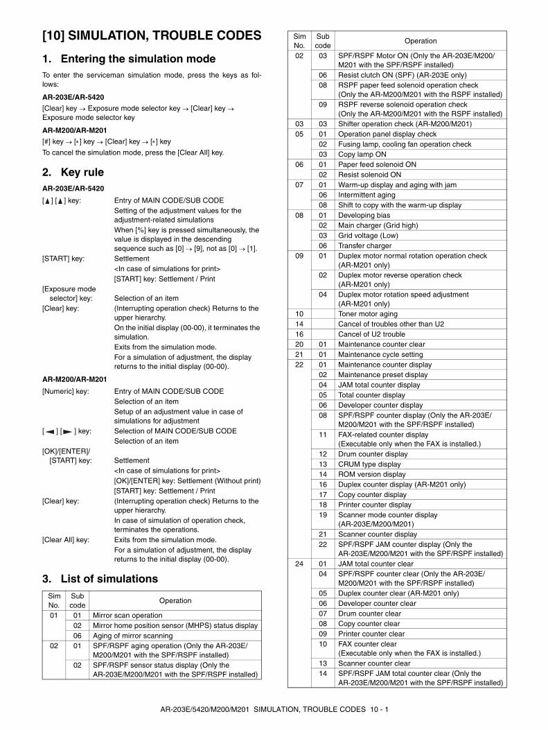
[10] SIMULATION, TROUBLE CODES
1. Entering the simulation modeTo enter the serviceman simulation mode, press the keys as fol-lows:
AR-203E/AR-5420
[Clear] key → Exposure mode selector key → [Clear] key → Exposure mode selector key
AR-M200/AR-M201
[#] key → [∗] key → [Clear] key → [∗] key
To cancel the simulation mode, press the [Clear All] key.
2. Key ruleAR-203E/AR-5420
AR-M200/AR-M201
3. List of simulations
[ ] [ ] key: Entry of MAIN CODE/SUB CODESetting of the adjustment values for the adjustment-related simulationsWhen [%] key is pressed simultaneously, the value is displayed in the descending sequence such as [0] → [9], not as [0] → [1].
[START] key: Settlement<In case of simulations for print>[START] key: Settlement / Print
[Exposure mode selector] key: Selection of an item
[Clear] key: (Interrupting operation check) Returns to the upper hierarchy.On the initial display (00-00), it terminates the simulation.Exits from the simulation mode.For a simulation of adjustment, the display returns to the initial display (00-00).
[Numeric] key: Entry of MAIN CODE/SUB CODESelection of an itemSetup of an adjustment value in case of simulations for adjustment
[ ] [ ] key: Selection of MAIN CODE/SUB CODESelection of an item
[OK]/[ENTER]/[START] key: Settlement
<In case of simulations for print>[OK]/[ENTER] key: Settlement (Without print)[START] key: Settlement / Print
[Clear] key: (Interrupting operation check) Returns to the upper hierarchy.In case of simulation of operation check, terminates the operations.
[Clear All] key: Exits from the simulation mode.For a simulation of adjustment, the display returns to the initial display (00-00).
Sim No.
Sub code
Operation
01 01 Mirror scan operation02 Mirror home position sensor (MHPS) status display06 Aging of mirror scanning
02 01 SPF/RSPF aging operation (Only the AR-203E/M200/M201 with the SPF/RSPF installed)
02 SPF/RSPF sensor status display (Only the AR-203E/M200/M201 with the SPF/RSPF installed)
02 03 SPF/RSPF Motor ON (Only the AR-203E/M200/M201 with the SPF/RSPF installed)
06 Resist clutch ON (SPF) (AR-203E only)08 RSPF paper feed solenoid operation check
(Only the AR-M200/M201 with the RSPF installed)09 RSPF reverse solenoid operation check
(Only the AR-M200/M201 with the RSPF installed)03 03 Shifter operation check (AR-M200/M201)05 01 Operation panel display check
02 Fusing lamp, cooling fan operation check03 Copy lamp ON
06 01 Paper feed solenoid ON02 Resist solenoid ON
07 01 Warm-up display and aging with jam06 Intermittent aging08 Shift to copy with the warm-up display
08 01 Developing bias02 Main charger (Grid high)03 Grid voltage (Low)06 Transfer charger
09 01 Duplex motor normal rotation operation check (AR-M201 only)
02 Duplex motor reverse operation check (AR-M201 only)
04 Duplex motor rotation speed adjustment (AR-M201 only)
10 Toner motor aging14 Cancel of troubles other than U216 Cancel of U2 trouble20 01 Maintenance counter clear21 01 Maintenance cycle setting22 01 Maintenance counter display
02 Maintenance preset display04 JAM total counter display05 Total counter display06 Developer counter display08 SPF/RSPF counter display (Only the AR-203E/
M200/M201 with the SPF/RSPF installed)11 FAX-related counter display
(Executable only when the FAX is installed.)12 Drum counter display13 CRUM type display14 ROM version display16 Duplex counter display (AR-M201 only)17 Copy counter display18 Printer counter display19 Scanner mode counter display
(AR-203E/M200/M201)21 Scanner counter display22 SPF/RSPF JAM counter display (Only the
AR-203E/M200/M201 with the SPF/RSPF installed)24 01 JAM total counter clear
04 SPF/RSPF counter clear (Only the AR-203E/M200/M201 with the SPF/RSPF installed)
05 Duplex counter clear (AR-M201 only)06 Developer counter clear07 Drum counter clear08 Copy counter clear09 Printer counter clear10 FAX counter clear
(Executable only when the FAX is installed.)13 Scanner counter clear14 SPF/RSPF JAM total counter clear (Only the
AR-203E/M200/M201 with the SPF/RSPF installed)
Sim No.
Sub code
Operation
AR-203E/5420/M200/M201 SIMULATION, TROUBLE CODES 10 - 1
24 15 Scanner mode counter clear (AR-203E/M200/M201)
25 01 Main motor operation check (Cooling fan motor rotation check)
10 Polygon motor ON26 02 SPF/RSPF setup
03 Second cassette setup04 Machine duplex setup06 Destination setup07 Machine conditions check20 Rear edge void setup30 CE mark support control ON/OFF37 Cancel of stop at developer life over39 Memory capacity check40 Polygon motor OFF time setup (Time required for
turning OFF after completion of printing)42 Transfer ON timing control setup43 Side void setup54 γ life correction setting62 Energy-save mode copy lamp setup
30 01 Paper sensor status display41 06 OC cover float detection level adjustment (Only the
AR-203E/M200/M201 with the SPF/RSPF installed)
07 OC cover float detection margin setting (Only the AR-203E/M200/M201 with the SPF/RSPF installed)
43 01 Fusing temperature setting (Normal copy)04 Fusing temperature setting in multi copy05 Fusing temperature setup in duplex copy
(AR-M201 only)14 Fusing start temperature setting
46 01 Copy density adjustment (300dpi)02 Copy density adjustment (600dpi)12 Density adjustment in the FAX mode
(Collective adjustment) (Executable only when the FAX is installed.)
13 FAX mode density adjustment (Normal text) (Executable only when the FAX is installed.)
14 FAX mode density adjustment (Fine text) (Executable only when the FAX is installed.)
15 FAX mode density adjustment (Super fine) (Executable only when the FAX is installed.)
18 Image contrast adjustment (300dpi)19 Exposure mode setup20 SPF/RSPF exposure correction (Only the
AR-203E/M200/M201 with the SPF/RSPF installed)29 Image contrast adjustment (600dpi)30 AE limit adjustment31 Image sharpness adjustment32 Copier color reproduction setup39 FAX mode sharpness adjustment
(Executable only when the FAX is installed.)48 01 Front/rear (main scanning) direction and scan (sub
scanning) direction magnification ratio adjustment05 SPF/RSPF mode sub scan direction magnification
ratio in copying (Only the AR-203E/M200/M201 with the SPF/RSPF installed)
49 01 Flash ROM program writing mode50 01 Lead edge image position
06 Copy lead edge position adjustment (SPF/RSPF) (Only the AR-203E/M200/M201 with the SPF/RSPF installed)
10 Center offset adjustment
Sim No.
Sub code
Operation
50 12 Document off-center adjustment18 Memory reverse position adjustment in duplex
copy (Only the AR-M201, or the AR-M200 with the RSPF installed)
19 Duplex copy rear edge void adjustment (AR-M201 only)
51 02 Resist quantity adjustment53 08 SPF/RSPF scan position automatic adjustment
(Only the AR-203E/M200/M201 with the SPF/RSPF installed)
61 03 Polygon motor check (HSYNC output check)63 01 Shading check
02 Black level automatic correction12 Light quantity stabilization wait time setting13 Light quantity stabilization band setting
64 01 Self print (1by2 mode)66 01 FAX soft SW setting
(Executable only when the FAX is installed.)02 FAX soft SW initializing
(excluding the adjustment values) (Executable only when the FAX is installed.)
03 FAX PWB memory check (Executable only when the FAX is installed.)
04 Signal send mode (Max. value) (Executable only when the FAX is installed.)
05 Signal send mode (Soft SW set value) (Executable only when the FAX is installed.)
07 Image memory content print (Executable only when the FAX is installed.)
10 Image memory content clear (Executable only when the FAX is installed.)
11 300bps signal send (Max. value) (Executable only when the FAX is installed.)
12 300bps signal send (Soft SW set value) (Executable only when the FAX is installed.)
13 Dial test (Executable only when the FAX is installed.)
17 DTMF signal send (Max. value) (Executable only when the FAX is installed.)
18 DTMF signal send (Soft SW set value) (Executable only when the FAX is installed.)
21 FAX information print (Executable only when the FAX is installed.)
24 FAST SRAM clear (Executable only when the FAX is installed.)
30 TEL/LIU status change check (Executable only when the FAX is installed.)
33 Signal detection check (Executable only when the FAX is installed.)
34 Communication time measurement (Executable only when the FAX is installed.)
37 Speaker sound volume setting (Executable only when the FAX is installed.)
38 Time setting/check (Executable only when the FAX is installed.)
67 50 USB receive speed adjustment (USB1.1) (AR-203E only)
Sim No.
Sub code
Operation
AR-203E/5420/M200/M201 SIMULATION, TROUBLE CODES 10 - 2

4. Descriptions of various simulationsMain code
Sub code
Contents Details of function/operation
01 01 Mirror scan operation [Function]When [OK]/[ENTER]/[START] key is pressed, the home position is checked and the mirror baseperforms full scan at the speed of the set magnification ratio.
During operation, the set magnification ratio is displayed.
The mirror home position sensor status is displayed with the "Drum replacement required lamp(or the copy mode indicator for the AR-M200/M201)". (When the mirror is in the home position,the lamp lights up.)
During operation, the copy lamp lights up.
When [Clear] key is pressed, if the operation is on the way, it is terminated and the machinegoes to the sub code entry standby mode.
[Operation] (AR-M200/M201)
02 Mirror home position sensor (MHPS) status display
[Function]Monitors the mirror home position sensor, and makes the "Drum replacement required lamp (orthe copy mode indicator for the AR-M200/M201)" turn on during the sensor ON status.
[Operation] (AR-M200/M201)
06 Aging of mirror scanning [Function]When [OK]/[ENTER]/[START] key is pressed, the mirror base performs full scan at the speed ofthe set magnification ratio.
During operation, the set magnification ratio is displayed.
After 3sec, the mirror base performs full scan again.
∗ When [OK]/[ENTER]/[START] key is pressed once, the ready lamp remains OFF.The mirror home position sensor status is displayed on the "Drum replacement required lamp(or the copy mode indicator for the AR-M200/M201)." (The lamp is ON when the mirror is in thehome position.)
During aging, the copy lamp is ON.
[Operation] (AR-M200/M201)The operation is similar to simulation 01-01.
02 01 SPF/RSPF aging operation (Only the AR-203E/M200/M201 with the SPF/RSPF installed)
[Function]When [OK]/[ENTER]/[START] key is pressed, the set magnification ratio is obtained. For theSPF, the single-face document transport is performed. For the RSPF, the duplex documenttransport is performed.
However, the operating conditions don't matter and the operation is not stopped even in case ofa jam. Also the magnification ratio is displayed on the LCD/display.
[Operation] (AR-M200/M201)The operation is similar to simulation 01-01.
1) Initial display 2) [ZOOM]/[COPY RATIO] key
2) [ ] key
2) [ ] key
3) [OK]/[ENTER]/[START]key01-01 SCAN CHK
- 100% + 01-01 SCAN CHK - 78% +
01-01 SCAN CHK - 99% +
01-01 SCAN CHK - 101% +
01-01 SCAN CHKEXECUTING... - 78% +
1) Initial display
01-02 MHP-SENSOREXECUTING...
AR-203E/5420/M200/M201 SIMULATION, TROUBLE CODES 10 - 3

02 02 SPF/RSPF sensor status display (Only the AR-203E/M200/M201 with the SPF/RSPF installed)
[Function]The ON/OFF status of the SPF/RSPF sensors can be checked with the LCD/LED.When a sensor is ON, the sensor name is displayed on the LCD/LED.
[Operation] (AR-M200/M201)
03 SPF/RSPF Motor ON (Only the AR-203E/M200/M201 with the SPF/RSPF installed)
[Function]When [OK]/[ENTER]/[START] key is pressed, the motor rotates for 10sec at the speed corre-sponding to the set magnification ratio.
[Operation] (AR-M200/M201)The operation is similar to simulation 01-01.
06 Resist clutch ON (SPF) (AR-203E only)
When the [START] key is pressed, the SPF resist clutch (SRRC) repeats ON (500 ms) and OFF (500 ms) 20 times.
08 RSPF paper feed solenoid operation check (Only the AR-M200/M201 with the RSPF installed)
[Function]The RSPF paper feed solenoid (SPUS) repeats ON for 500ms and OFF for 500ms 20 times bythe use of the solenoid drive control Bios.
[Operation]
09 RSPF reverse solenoid operation check (Only the AR-M200/M201 with the RSPF installed)
[Function]The RSPF reverse solenoid (SPFS) repeats ON for 500ms and OFF for 500ms 20 times by theuse of the solenoid drive control Bios.
[Operation]
03 03 Shifter operation check (AR-M200/M201)
[Function]The shifter is moved back and forth in four reciprocations.
[Operation]
Main code
Sub code
Contents Details of function/operation
SensorDisplay item
(AR-M200/M201)Display item(AR-203E)
Document set sensor SPID TD cartridge replacement required lamp
RSPF document transport sensor SPPD Misfeed lampRSPF paper feed cover open/close sensor
SDSW —
RSPF paper exit sensor SPOD —
1) Initial display 2) When the sensor is ON:
02-02 SPF SENSOR 02-02 SPF SENSORSPID SPPD SDSW SPOD
1) Initial display
02-08 SPF SPUS CHKEXECUTING...
1) Initial display
02-09 RSPF SPFS CHKEXECUTING...
1) Initial display
03-03 SHIFTER CHKEXECUTING...
AR-203E/5420/M200/M201 SIMULATION, TROUBLE CODES 10 - 4

05 01 Operation panel display check
[Function]<LED check mode (All ON/Individual ON)>When [OK]/[ENTER]/[START] key is pressed, all the LCD's on the operation panel are turnedON (all pixels ON).After 5sec of ON, the machine goes into the sub code entry standby mode.When [Mode Select] key is pressed under the all ON state, the mode is shifted to the individualON mode, where the LED's are turned on one by one from the left upper end to the left lowerside then from the right upper side to the right lower side. (All the pixels of LCD are lightedsimultaneously.) After lighting all the LCD's sequentially, all the LCD's are lighted simulta-neously. After 5sec from lighting all the LCD's simultaneously, the machine goes into the subcode entry standby mode. (Cycle of individual ON mode: ON 300ms, OFF 20ms)
When [Clear] key is pressed in the LED check mode, the machine goes into the sub code entrystandby mode.When [START] key is pressed, the machine goes into the key input check mode.
<Key input check mode>When the machine goes into the key input check mode, the value display section indicates "– ––" (For the AR-M200/M201, 0 of the LCD is indicated).When any key is pressed after pressing a key on the operation panel, "+1" is added to thevalue.Once a key is pressed, it is not recounted.When [START] key is pressed, counting is made and the machine goes into the LED ON checkmode (LED all ON status) after 3sec.When [Clear] key is pressed for the first time, it is counted. When it is pressed for the secondtime, the key check mode is retained as well as when another key is pressed.
(Note in the key input check mode)• Be sure to press [START] key at the last. (If it is pressed on the way, the machine goes into
the LED ON check mode.) (LED all ON status)
• Multi key input is ignored.
[Operation] (AR-M200/M201)<LED check mode (All ON/Individual ON)>
<Key input check mode>
02 Fusing lamp, cooling fan operation check
[Function]When [OK]/[ENTER]/[START] key is pressed, the fusing lamp repeats ON for 500ms and OFFfor 500ms 5 times. During this period, the cooling fan motor rotates.
Note: When the CE mark setting is ON, the slow start function may operate depending on theemployed frequency. If the state of the heater lamp cannot be checked, temporarily set SIM 26-30 to "0" and check the lamp state. After confirming that the heater lamp is ON, set SIM 26-30to "1" again.
[Operation] (AR-M200/M201)
03 Copy lamp ON [Function]When [OK]/[ENTER]/[START] key is pressed, the copy lamp turns ON for 5sec.
[Operation] (AR-M200/M201)
Main code
Sub code
Contents Details of function/operation
1) Initial display
2) When [Mode Select] key is pressed, the machine goes into the individual ON mode.
1) Initial display 2) [OK]/[ENTER]/[START]key
05-01 LCD/LED CHK. 0 05-01 LCD/LED CHK.
**
1) Initial display
05-02 HT LAMP CHKEXECUTING...
1) Initial display
05-03 C-LAMP CHKEXECUTING...
AR-203E/5420/M200/M201 SIMULATION, TROUBLE CODES 10 - 5
06 01 Paper feed solenoid ON [Function]When [OK]/[ENTER]/[START] key is pressed, the selected paper feed solenoid repeats ON for500ms and OF for 500ms 20 times.When tray select key (or [Numeric] key or [ ] [ ] key for the AR-M200/M201) is pressed,the paper feed solenoid setting is switched.
[Operation] (AR-M200/M201)
02 Resist solenoid ON [Function]When [OK]/[ENTER]/[START] key is pressed, the resist solenoid repeats ON for 500ms andOFF for 500ms 20 times.
[Operation] (AR-M200/M201)
07 01 Warm-up display and aging with jam
[Function]Copying is repeated to make the set quantity of copies.When the simulation is executed, warm-up is started and warm-up time is added for every sec-ond from 0 and displayed.When warm-up is completed, addition is stopped. When [Clear All] key is pressed, the readylamp lights up.After that, enter the copy quantity with [ ] [ ] key (or [Numeric] key for the AR-M200/M201)and press [OK]/[ENTER]/[START] key to repeat copying of the set quantity (interval 0sec).To cancel the simulation, turn off the power or execute a simulation which causes hardwarereset.
[Operation] (AR-M200/M201)
06 Intermittent aging [Function]Copying is repeated to make the set quantity of copies.When the simulation is executed, warm-up is performed and the ready lamp is lighted.Enter the copy quantity with the [ ] [ ] key (or [Numeric] key for the AR-M200/M201) andpress [OK]/[ENTER]/[START] key, and copying is executed to make the set quantity of copies,and the ready state is kept for 3sec, and copying is executed again to make the set quantity ofcopies. These operations are repeated.To cancel the simulation, turn off the power or execute a simulation which executes hardware reset.
[Operation] (AR-M200/M201)
08 Shift to copy with the warm-up display
[Function]Enter the simulation code, and warm-up is started and warm-up time is counted for every sec-ond from 0 and displayed.When [Clear All] key is pressed during counting up, "0" is displayed on the display and countingis stopped. However, warm-up is continued.After completion of warm-up, counting is terminated. (The aging function is removed from simu-lation 07-01.)
[Operation] (AR-M200/M201)
Main code
Sub code
Contents Details of function/operation
Code number Setting Remark0 CPFS11 CPFS2 Operation is possible only when No. 2 cassette is installed. 2 MPFS
1) Initial display 2) [Numeric] key or [ ] key
2) [Numeric] key or [ ] key
3) [OK]/[ENTER]/[START]key
4) Returns to the initial display.
06-01 PSOL CHK0:CPFS1
06-01 PSOL CHK1:CPFS2
06-01 PSOL CHK2:MPFS
06-01 PSOL CHKEXECUTING...
1) Initial display
06-02 RES.R SOL CHKEXECUTING...
1) Initial display 2) After 10sec
07-01 W-UP/AGING 0
07-01 W-UP/AGING 10
1) Initial display (Basic display of copy)
READY TO COPY 100% A4 0
1) Initial display 2) After 10sec
07-08 W-UP C-MODE 0
07-08 W-UP C-MODE 10
AR-203E/5420/M200/M201 SIMULATION, TROUBLE CODES 10 - 6

08 01 Developing bias [Function]When [OK]/[ENTER]/[START] key is pressed, the developing bias signal is turned ON for 30sec.
When, however, an actual output value is measured, use simulation 25-01.
After completion of this process, the machine goes into the sub code entry standby mode.
[Operation] (AR-M200/M201)
02 Main charger (Grid high) [Function]When [OK]/[ENTER]/[START] key is pressed, the main charger is outputted for 30sec in the gridvoltage HIGH move.
After completion of this process, the machine goes into the sub code entry standby mode.
[Operation] (AR-M200/M201)
03 Grid voltage (Low) [Function]When [OK]/[ENTER]/[START] key is pressed, the main charger is outputted for 30sec in the gridvoltage LOW move.
After completion of this process, the machine goes into the sub code entry standby mode.
[Operation] (AR-M200/M201)
06 Transfer charger [Function]When [OK]/[ENTER]/[START] key is pressed, the transfer charger is outputted for 30sec.
After completion of this process, the machine goes into the sub code entry standby mode.
[Operation] (AR-M200/M201)
09 01 Duplex motor normal rotation operation check (AR-M201 only)
[Function]Use the duplex motor Bios to drive the duplex motor in the normal direction (paper exit direc-tion) for 30sec.
After completion of this process, the machine goes into the sub code entry standby mode.
[Operation]
02 Duplex motor reverse operation check (AR-M201 only)
[Function]Use the duplex motor Bios to drive the duplex motor in the reverse direction for 30sec.
After completion of this process, the machine goes into the sub code entry standby mode.
[Operation]
04 Duplex motor rotation speed adjustment (AR-M201 only)
[Function]When this simulation is executed, the currently set value is displayed.Enter the adjustment value with [Numeric] key and press [OK]/[ENTER]/[START] key. Theentered value is stored and the machine goes into the sub code entry standby mode. Thegreater the set value is, the higher the speed is. The smaller the set value is, the lower thespeed is. (Setting range: 1 - 13, Default: 8)
[Operation]
Main code
Sub code
Contents Details of function/operation
1) Initial display
08-01 DVLP BIAS SET.EXECUTING...
1) Initial display
08-02 MHV(H) SET.EXECUTING...
1) Initial display
08-03 MHV(L) SET.EXECUTING...
1) Initial display
08-06 THV SET.EXECUTING...
1) Initial display
09-01 DPLX ROT.EXECUTING...
1) Initial display
09-02 DPLX ROT.REV.EXECUTING...
1) Initial display 2) [Numeric] key 3) [OK]/[ENTER]/[START]key
09-04 DPLX ROT.SPEED 8( 1-13)
09-04 DPLX ROT.SPEED 7( 1-13) 09-04 DPLX ROT.SPEED
7( 1-13)
AR-203E/5420/M200/M201 SIMULATION, TROUBLE CODES 10 - 7
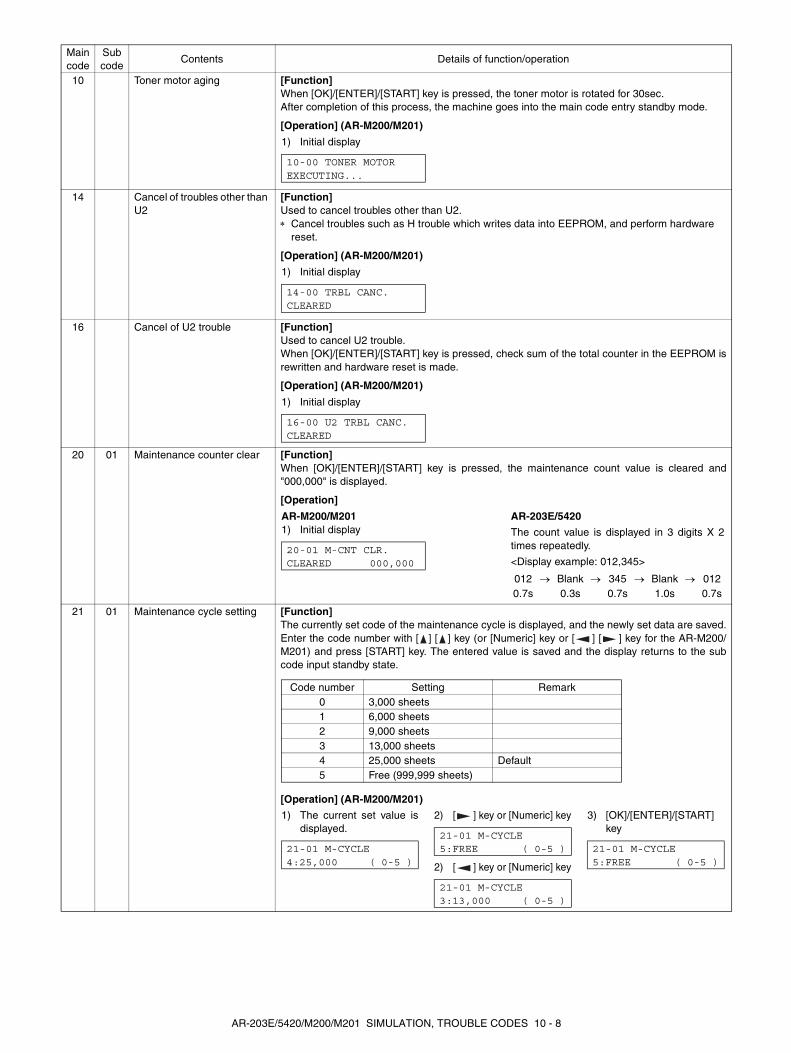
10 Toner motor aging [Function]When [OK]/[ENTER]/[START] key is pressed, the toner motor is rotated for 30sec.After completion of this process, the machine goes into the main code entry standby mode.
[Operation] (AR-M200/M201)
14 Cancel of troubles other than U2
[Function]Used to cancel troubles other than U2.∗ Cancel troubles such as H trouble which writes data into EEPROM, and perform hardware
reset.
[Operation] (AR-M200/M201)
16 Cancel of U2 trouble [Function]Used to cancel U2 trouble.When [OK]/[ENTER]/[START] key is pressed, check sum of the total counter in the EEPROM isrewritten and hardware reset is made.
[Operation] (AR-M200/M201)
20 01 Maintenance counter clear [Function]When [OK]/[ENTER]/[START] key is pressed, the maintenance count value is cleared and"000,000" is displayed.
[Operation]
21 01 Maintenance cycle setting [Function]The currently set code of the maintenance cycle is displayed, and the newly set data are saved.Enter the code number with [ ] [ ] key (or [Numeric] key or [ ] [ ] key for the AR-M200/M201) and press [START] key. The entered value is saved and the display returns to the subcode input standby state.
[Operation] (AR-M200/M201)
Main code
Sub code
Contents Details of function/operation
1) Initial display
10-00 TONER MOTOREXECUTING...
1) Initial display
14-00 TRBL CANC.CLEARED
1) Initial display
16-00 U2 TRBL CANC.CLEARED
AR-M200/M2011) Initial display
AR-203E/5420
The count value is displayed in 3 digits X 2times repeatedly.
<Display example: 012,345>20-01 M-CNT CLR.CLEARED 000,000
012 → Blank → 345 → Blank → 0120.7s 0.3s 0.7s 1.0s 0.7s
Code number Setting Remark0 3,000 sheets1 6,000 sheets2 9,000 sheets3 13,000 sheets4 25,000 sheets Default5 Free (999,999 sheets)
1) The current set value isdisplayed.
2) [ ] key or [Numeric] key
2) [ ] key or [Numeric] key
3) [OK]/[ENTER]/[START]key
21-01 M-CYCLE4:25,000 ( 0-5 )
21-01 M-CYCLE5:FREE ( 0-5 )
21-01 M-CYCLE3:13,000 ( 0-5 )
21-01 M-CYCLE5:FREE ( 0-5 )
AR-203E/5420/M200/M201 SIMULATION, TROUBLE CODES 10 - 8

22 01 Maintenance counter display [Function]When [OK]/[ENTER]/[START] key is pressed, the maintenance counter is displayed.
[Operation]
02 Maintenance preset display [Function]When [OK]/[ENTER]/[START] key is pressed, the preset value (25,000 sheets, etc.) corre-sponding to the code set with simulation 21-01 is displayed.
[Operation]
04 JAM total counter display [Function]The JAM total counter is displayed.
[Operation]
05 Total counter display [Function]The total counter value is displayed.
[Operation]
06 Developer counter display [Function]When [OK]/[ENTER]/[START] key is pressed, the developer counter value is obtained and dis-played.
[Operation]
08 SPF/RSPF counter display (Only the AR-203E/M200/M201 with the SPF/RSPF installed)
[Function]The SPF/RSPF counter is displayed.
[Operation]
11 FAX-related counter display (Executable only when the FAX is installed.)
[Function]The FAX-related counter is displayed.
[Operation]
Main code
Sub code
Contents Details of function/operation
AR-M200/M201
1) Initial display
AR-203E/5420
The operation is similar to simulation 20-01.
22-01 M-CNT ***,***
AR-M200/M201
1) Initial display
AR-203E/5420
The operation is similar to simulation 20-01.
22-02 M-CNT PRESET ***,***
AR-M200/M201
1) Initial display
AR-203E/5420
The operation is similar to simulation 20-01.
22-04 JAM TTL CNT ***,***
AR-M200/M201
1) Initial display
AR-203E/5420
The operation is similar to simulation 20-01.
22-05 TTL CNT ***,***
AR-M200/M201
1) Initial display
AR-203E/5420
The operation is similar to simulation 20-01.
22-06 DVLP CNT ***,***
AR-M200/M201
1) Initial display
AR-203E
The operation is similar to simulation 20-01.
22-08 SPF CNT ***,***
1) Initial display
∗ [Clear] key: FAX control is terminated.
2) Select 1
("xxx,xxx" is the current value.)
∗ [Clear] key: Returns to "1) Initial display".
2) Select 2
("xxxxx: xx. xx" is the current value.)
∗ [Clear] key: Returns to "1) Initial display".
SELECT COUNTER1:PAGE 2:TIME
SEND PAGE:xxx,xxxRECV PAGE:xxx,xxx
TX TIME:xxxxx:xx.xxRX TIME:xxxxx:xx.xx
AR-203E/5420/M200/M201 SIMULATION, TROUBLE CODES 10 - 9

22 12 Drum counter display [Function]The drum counter is displayed.
[Operation]
13 CRUM type display [Function]The CRUM type currently set (written) in the CRUM chip is displayed.
[Operation] (AR-M200/M201)
14 ROM version display [Function]The P-ROM version is displayed.Press [ ] [ ] key (or [Numeric] key or [ ] [ ] key for the AR-M200/M201) to switch the dis-play version.
[Operation]
16 Duplex counter display (AR-M201 only)
[Function]The duplex counter is displayed.
[Operation]
17 Copy counter display [Function]The copy counter is displayed.
[Operation]
Main code
Sub code
Contents Details of function/operation
AR-M200/M201
1) Initial display
AR-203E/5420
The operation is similar to simulation 20-01.
22-12 DRUM CNT ***,***
Code number CRUM type Display item00 Not set 001 BTA-A BTA-A02 BTA-B BTA-B03 BTA-C BTA-C99 Conversion CONVERSION
1) The CRUM type is displayed.
22-13 CRUM TYPE01:BTA-A
Code number Version Display item0 Main unit Program MAIN PROG.1 F-IMC Program F-IMC PROG.2 LCD DATA LCD DATA
AR-M200/M201
1) Initial display
2) [Numeric] key or [ ] key
2) [Numeric] key or [ ] key
AR-203E/5420
The operation is similar to simulation 20-01.
22-14 ROM VER.MAIN PROG. 00.00
22-14 ROM VER.F-IMC PROG. 00.00
22-14 ROM VER.LCD DATA 00.00
1) Initial display
22-16 DPLX CNT ***,***
AR-M200/M201
1) Initial display
AR-203E/5420
The operation is similar to simulation 20-01.
22-17 COPIES CNT ***,***
AR-203E/5420/M200/M201 SIMULATION, TROUBLE CODES 10 - 10
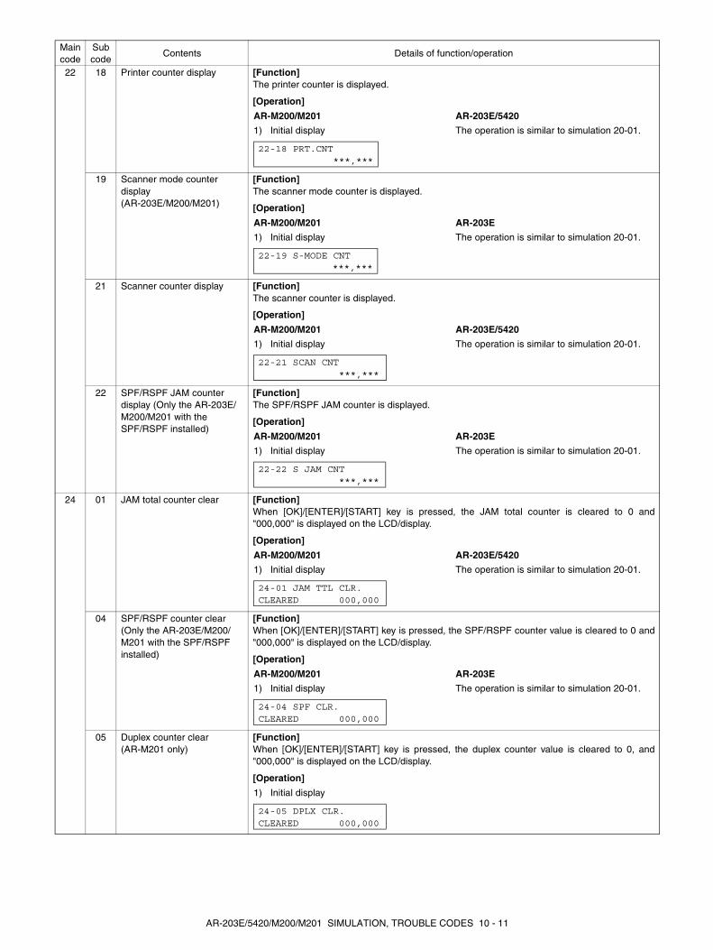
22 18 Printer counter display [Function]The printer counter is displayed.
[Operation]
19 Scanner mode counter display (AR-203E/M200/M201)
[Function]The scanner mode counter is displayed.
[Operation]
21 Scanner counter display [Function]The scanner counter is displayed.
[Operation]
22 SPF/RSPF JAM counter display (Only the AR-203E/M200/M201 with the SPF/RSPF installed)
[Function]The SPF/RSPF JAM counter is displayed.
[Operation]
24 01 JAM total counter clear [Function]When [OK]/[ENTER]/[START] key is pressed, the JAM total counter is cleared to 0 and"000,000" is displayed on the LCD/display.
[Operation]
04 SPF/RSPF counter clear (Only the AR-203E/M200/M201 with the SPF/RSPF installed)
[Function]When [OK]/[ENTER]/[START] key is pressed, the SPF/RSPF counter value is cleared to 0 and"000,000" is displayed on the LCD/display.
[Operation]
05 Duplex counter clear (AR-M201 only)
[Function]When [OK]/[ENTER]/[START] key is pressed, the duplex counter value is cleared to 0, and"000,000" is displayed on the LCD/display.
[Operation]
Main code
Sub code
Contents Details of function/operation
AR-M200/M201
1) Initial display
AR-203E/5420
The operation is similar to simulation 20-01.
22-18 PRT.CNT ***,***
AR-M200/M201
1) Initial display
AR-203E
The operation is similar to simulation 20-01.
22-19 S-MODE CNT ***,***
AR-M200/M201
1) Initial display
AR-203E/5420
The operation is similar to simulation 20-01.
22-21 SCAN CNT ***,***
AR-M200/M201
1) Initial display
AR-203E
The operation is similar to simulation 20-01.
22-22 S JAM CNT ***,***
AR-M200/M201
1) Initial display
AR-203E/5420
The operation is similar to simulation 20-01.
24-01 JAM TTL CLR.CLEARED 000,000
AR-M200/M201
1) Initial display
AR-203E
The operation is similar to simulation 20-01.
24-04 SPF CLR.CLEARED 000,000
1) Initial display
24-05 DPLX CLR.CLEARED 000,000
AR-203E/5420/M200/M201 SIMULATION, TROUBLE CODES 10 - 11
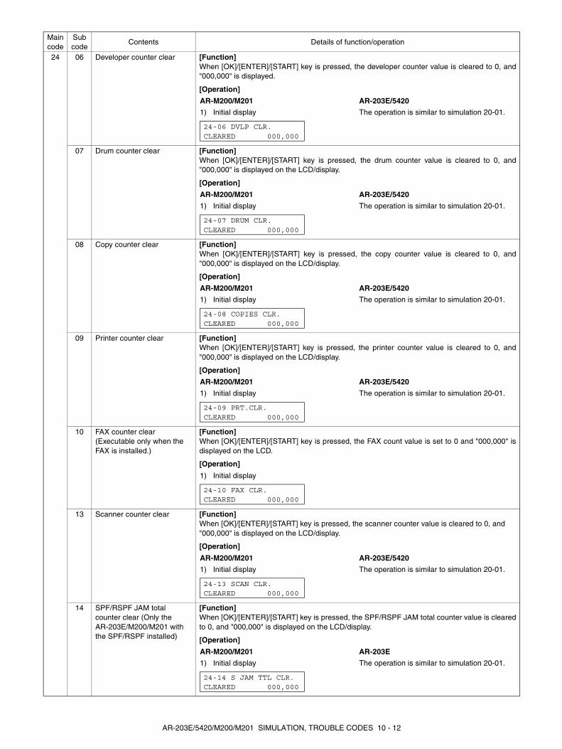
24 06 Developer counter clear [Function]When [OK]/[ENTER]/[START] key is pressed, the developer counter value is cleared to 0, and"000,000" is displayed.
[Operation]
07 Drum counter clear [Function]When [OK]/[ENTER]/[START] key is pressed, the drum counter value is cleared to 0, and"000,000" is displayed on the LCD/display.
[Operation]
08 Copy counter clear [Function]When [OK]/[ENTER]/[START] key is pressed, the copy counter value is cleared to 0, and"000,000" is displayed on the LCD/display.
[Operation]
09 Printer counter clear [Function]When [OK]/[ENTER]/[START] key is pressed, the printer counter value is cleared to 0, and"000,000" is displayed on the LCD/display.
[Operation]
10 FAX counter clear (Executable only when the FAX is installed.)
[Function]When [OK]/[ENTER]/[START] key is pressed, the FAX count value is set to 0 and "000,000" isdisplayed on the LCD.
[Operation]
13 Scanner counter clear [Function]When [OK]/[ENTER]/[START] key is pressed, the scanner counter value is cleared to 0, and "000,000" is displayed on the LCD/display.
[Operation]
14 SPF/RSPF JAM total counter clear (Only the AR-203E/M200/M201 with the SPF/RSPF installed)
[Function]When [OK]/[ENTER]/[START] key is pressed, the SPF/RSPF JAM total counter value is clearedto 0, and "000,000" is displayed on the LCD/display.
[Operation]
Main code
Sub code
Contents Details of function/operation
AR-M200/M201
1) Initial display
AR-203E/5420
The operation is similar to simulation 20-01.
24-06 DVLP CLR.CLEARED 000,000
AR-M200/M201
1) Initial display
AR-203E/5420
The operation is similar to simulation 20-01.
24-07 DRUM CLR.CLEARED 000,000
AR-M200/M201
1) Initial display
AR-203E/5420
The operation is similar to simulation 20-01.
24-08 COPIES CLR.CLEARED 000,000
AR-M200/M201
1) Initial display
AR-203E/5420
The operation is similar to simulation 20-01.
24-09 PRT.CLR.CLEARED 000,000
1) Initial display
24-10 FAX CLR.CLEARED 000,000
AR-M200/M201
1) Initial display
AR-203E/5420
The operation is similar to simulation 20-01.
24-13 SCAN CLR.CLEARED 000,000
AR-M200/M201
1) Initial display
AR-203E
The operation is similar to simulation 20-01.
24-14 S JAM TTL CLR.CLEARED 000,000
AR-203E/5420/M200/M201 SIMULATION, TROUBLE CODES 10 - 12
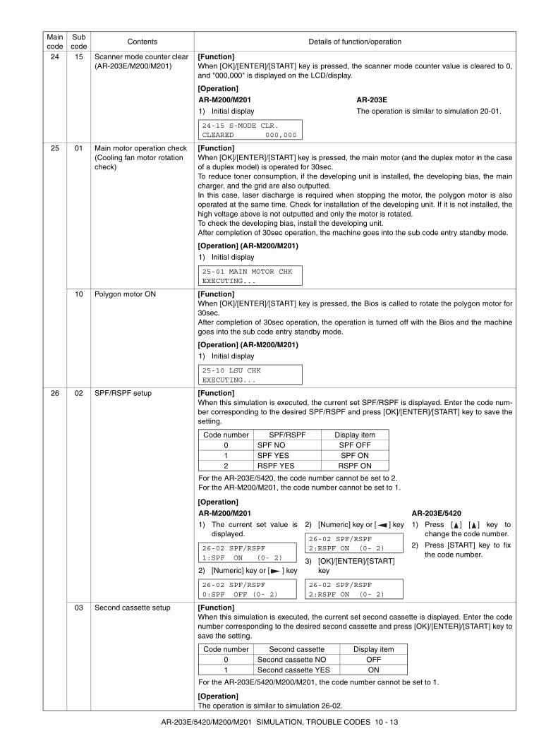
24 15 Scanner mode counter clear (AR-203E/M200/M201)
[Function]When [OK]/[ENTER]/[START] key is pressed, the scanner mode counter value is cleared to 0,and "000,000" is displayed on the LCD/display.
[Operation]
25 01 Main motor operation check (Cooling fan motor rotation check)
[Function]When [OK]/[ENTER]/[START] key is pressed, the main motor (and the duplex motor in the caseof a duplex model) is operated for 30sec.To reduce toner consumption, if the developing unit is installed, the developing bias, the maincharger, and the grid are also outputted.In this case, laser discharge is required when stopping the motor, the polygon motor is alsooperated at the same time. Check for installation of the developing unit. If it is not installed, thehigh voltage above is not outputted and only the motor is rotated.To check the developing bias, install the developing unit.After completion of 30sec operation, the machine goes into the sub code entry standby mode.
[Operation] (AR-M200/M201)
10 Polygon motor ON [Function]When [OK]/[ENTER]/[START] key is pressed, the Bios is called to rotate the polygon motor for30sec.After completion of 30sec operation, the operation is turned off with the Bios and the machinegoes into the sub code entry standby mode.
[Operation] (AR-M200/M201)
26 02 SPF/RSPF setup [Function]When this simulation is executed, the current set SPF/RSPF is displayed. Enter the code num-ber corresponding to the desired SPF/RSPF and press [OK]/[ENTER]/[START] key to save thesetting.
[Operation]
03 Second cassette setup [Function]When this simulation is executed, the current set second cassette is displayed. Enter the codenumber corresponding to the desired second cassette and press [OK]/[ENTER]/[START] key tosave the setting.
[Operation]The operation is similar to simulation 26-02.
Main code
Sub code
Contents Details of function/operation
AR-M200/M201
1) Initial display
AR-203E
The operation is similar to simulation 20-01.
24-15 S-MODE CLR.CLEARED 000,000
1) Initial display
25-01 MAIN MOTOR CHKEXECUTING...
1) Initial display
25-10 LSU CHKEXECUTING...
For the AR-203E/5420, the code number cannot be set to 2.For the AR-M200/M201, the code number cannot be set to 1.
Code number SPF/RSPF Display item0 SPF NO SPF OFF1 SPF YES SPF ON2 RSPF YES RSPF ON
AR-M200/M201
1) The current set value isdisplayed.
2) [Numeric] key or [ ] key
2) [Numeric] key or [ ] key
3) [OK]/[ENTER]/[START]key
AR-203E/5420
1) Press [ ] [ ] key tochange the code number.
2) Press [START] key to fixthe code number.
26-02 SPF/RSPF1:SPF ON (0- 2)
26-02 SPF/RSPF0:SPF OFF (0- 2)
26-02 SPF/RSPF2:RSPF ON (0- 2)
26-02 SPF/RSPF2:RSPF ON (0- 2)
For the AR-203E/5420/M200/M201, the code number cannot be set to 1.
Code number Second cassette Display item0 Second cassette NO OFF1 Second cassette YES ON
AR-203E/5420/M200/M201 SIMULATION, TROUBLE CODES 10 - 13

26 04 Machine duplex setup [Function]When this simulation is executed, the current set duplex is displayed. Enter the code numbercorresponding to the desired duplex and press [OK]/[ENTER]/[START] key to save the setting.
[Operation]The operation is similar to simulation 26-02.
06 Destination setup [Function]When this simulation is executed, the current set destination is displayed. Enter the code num-ber corresponding to the desired destination and press [OK]/[ENTER]/[START] key to save thesetting.
[Operation]The operation is similar to simulation 26-02.
07 Machine conditions check [Function]When this simulation is executed, the current machine setting is displayed.
[Operation] (AR-M200/M201)
20 Rear edge void setup [Function]When this simulation is executed, the current set rear edge void is displayed. Enter the codenumber corresponding to the desired rear edge void and press [OK]/[ENTER]/[START] key tosave the setting.
[Operation]The operation is similar to simulation 26-02.
30 CE mark support control ON/OFF
[Function]When this simulation is executed, the current set CE mark support control is displayed. Enterthe code number corresponding to the desired CE mark support control and press [OK]/[ENTER]/[START] key to save the setting.
[Operation]The operation is similar to simulation 26-02.
37 Cancel of stop at developer life over
[Function]When this simulation is executed, the current setting is displayed. Enter the code number andpress [OK]/[ENTER]/[START] key to change the setting.
[Operation]The operation is similar to simulation 21-01.
39 Memory capacity check [Function]When the simulation is executed, the currently installed SDRAM of the main unit is displayed.
[Operation] (AR-M200/M201)
Main code
Sub code
Contents Details of function/operation
* AR-203E/5420/M200: cannot be executed.
Code number Duplex Display item0 Duplex NO OFF1 Duplex YES* ON
* Code number 2 cannot be selected.
Code number Destination Display item0 Inch series INCH1 EX Japan AB series AB2 Japan AB series –
CPM Copy quantity Remark20 CPM 20
1) The machine setting is displayed.
26-07 CPM20 CPM
Code number Setting Display item Remark0 Rear edge void NO OFF1 Rear edge void YES ON Default
Code number Setting Display item Remark0 CE mark support control OFF OFF Default (100V series)1 CE mark support control ON ON
Code number Setting Remark8 8 MBYTE16 16 MBYTE
1) Memory capacity display
26-39 MEM.CHK8 MBYTE
AR-203E/5420/M200/M201 SIMULATION, TROUBLE CODES 10 - 14
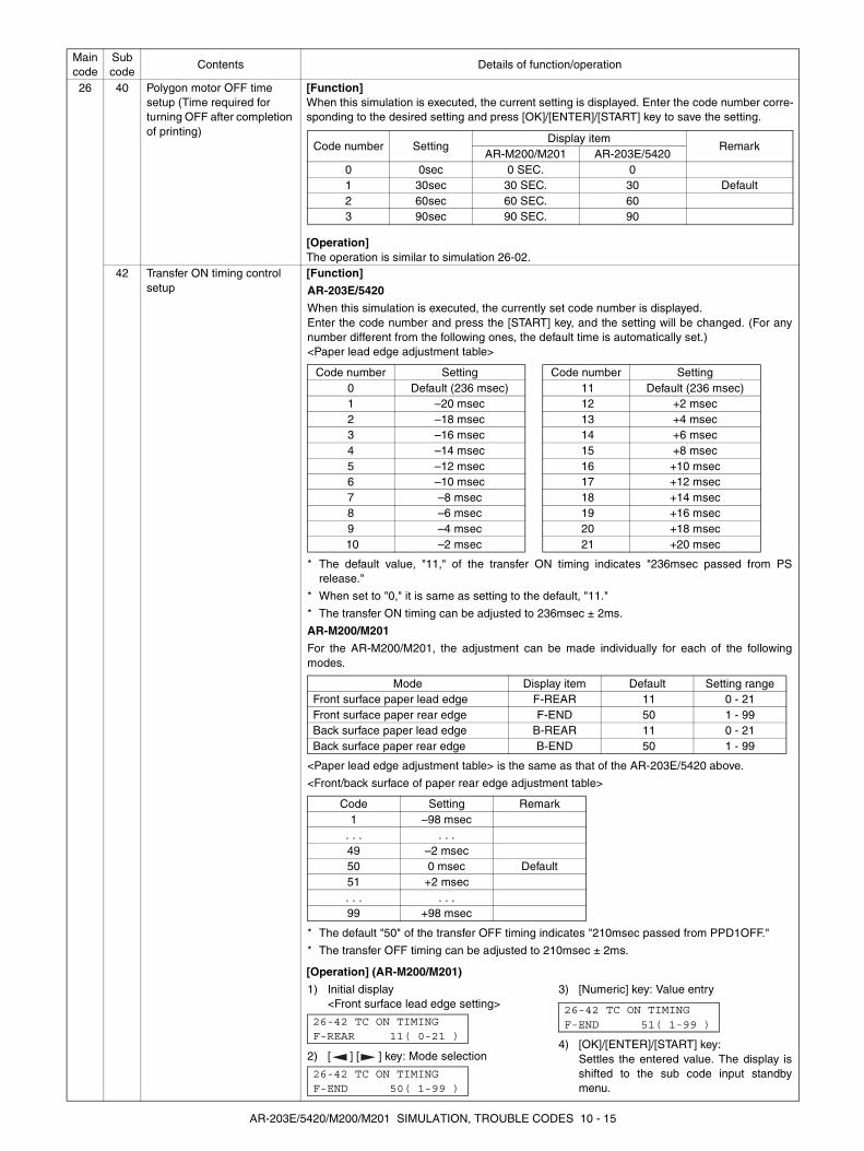
26 40 Polygon motor OFF time setup (Time required for turning OFF after completion of printing)
[Function]When this simulation is executed, the current setting is displayed. Enter the code number corre-sponding to the desired setting and press [OK]/[ENTER]/[START] key to save the setting.
[Operation]The operation is similar to simulation 26-02.
42 Transfer ON timing control setup
[Function]
[Operation] (AR-M200/M201)
Main code
Sub code
Contents Details of function/operation
Code number SettingDisplay item
RemarkAR-M200/M201 AR-203E/5420
0 0sec 0 SEC. 01 30sec 30 SEC. 30 Default2 60sec 60 SEC. 603 90sec 90 SEC. 90
AR-203E/5420
When this simulation is executed, the currently set code number is displayed.Enter the code number and press the [START] key, and the setting will be changed. (For anynumber different from the following ones, the default time is automatically set.)<Paper lead edge adjustment table>
* The default value, "11," of the transfer ON timing indicates "236msec passed from PSrelease."
* When set to "0," it is same as setting to the default, "11."
* The transfer ON timing can be adjusted to 236msec ± 2ms.
AR-M200/M201
For the AR-M200/M201, the adjustment can be made individually for each of the followingmodes.
<Paper lead edge adjustment table> is the same as that of the AR-203E/5420 above.
<Front/back surface of paper rear edge adjustment table>
* The default "50" of the transfer OFF timing indicates "210msec passed from PPD1OFF."
* The transfer OFF timing can be adjusted to 210msec ± 2ms.
Code number Setting Code number Setting0 Default (236 msec) 11 Default (236 msec)1 –20 msec 12 +2 msec2 –18 msec 13 +4 msec3 –16 msec 14 +6 msec4 –14 msec 15 +8 msec5 –12 msec 16 +10 msec6 –10 msec 17 +12 msec7 –8 msec 18 +14 msec8 –6 msec 19 +16 msec9 –4 msec 20 +18 msec
10 –2 msec 21 +20 msec
Mode Display item Default Setting rangeFront surface paper lead edge F-REAR 11 0 - 21Front surface paper rear edge F-END 50 1 - 99Back surface paper lead edge B-REAR 11 0 - 21Back surface paper rear edge B-END 50 1 - 99
Code Setting Remark1 –98 msec
. . . . . .49 –2 msec50 0 msec Default51 +2 msec. . . . . .99 +98 msec
1) Initial display <Front surface lead edge setting>
2) [ ] [ ] key: Mode selection
3) [Numeric] key: Value entry
4) [OK]/[ENTER]/[START] key: Settles the entered value. The display isshifted to the sub code input standbymenu.
26-42 TC ON TIMINGF-REAR 11( 0-21 )
26-42 TC ON TIMINGF-END 50( 1-99 )
26-42 TC ON TIMINGF-END 51( 1-99 )
AR-203E/5420/M200/M201 SIMULATION, TROUBLE CODES 10 - 15
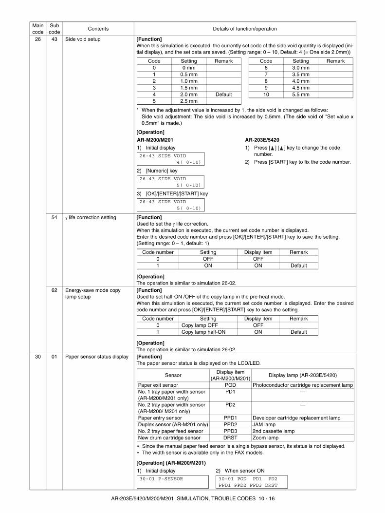
26 43 Side void setup [Function]When this simulation is executed, the currently set code of the side void quantity is displayed (ini-tial display), and the set data are saved. (Setting range: 0 – 10, Default: 4 (= One side 2.0mm))
* When the adjustment value is increased by 1, the side void is changed as follows:Side void adjustment: The side void is increased by 0.5mm. (The side void of "Set value x0.5mm" is made.)
[Operation]
54 γ life correction setting [Function]Used to set the γ life correction.When this simulation is executed, the current set code number is displayed.Enter the desired code number and press [OK]/[ENTER]/[START] key to save the setting. (Setting range: 0 – 1, default: 1)
[Operation]The operation is similar to simulation 26-02.
62 Energy-save mode copy lamp setup
[Function]Used to set half-ON /OFF of the copy lamp in the pre-heat mode.When this simulation is executed, the current set code number is displayed. Enter the desiredcode number and press [OK]/[ENTER]/[START] key to save the setting.
[Operation]The operation is similar to simulation 26-02.
30 01 Paper sensor status display [Function]The paper sensor status is displayed on the LCD/LED.
[Operation] (AR-M200/M201)
Main code
Sub code
Contents Details of function/operation
Code Setting Remark0 0 mm1 0.5 mm2 1.0 mm3 1.5 mm4 2.0 mm Default5 2.5 mm
Code Setting Remark6 3.0 mm7 3.5 mm8 4.0 mm9 4.5 mm10 5.5 mm
AR-M200/M201
1) Initial display
2) [Numeric] key
3) [OK]/[ENTER]/[START] key
AR-203E/5420
1) Press [ ] [ ] key to change the code number.
2) Press [START] key to fix the code number.26-43 SIDE VOID 4( 0-10)
26-43 SIDE VOID 5( 0-10)
26-43 SIDE VOID 5( 0-10)
Code number Setting Display item Remark0 OFF OFF1 ON ON Default
Code number Setting Display item Remark0 Copy lamp OFF OFF1 Copy lamp half-ON ON Default
∗ Since the manual paper feed sensor is a single bypass sensor, its status is not displayed.∗ The width sensor is available only in the FAX models.
SensorDisplay item
(AR-M200/M201)Display lamp (AR-203E/5420)
Paper exit sensor POD Photoconductor cartridge replacement lampNo. 1 tray paper width sensor (AR-M200/M201 only)
PD1 —
No. 2 tray paper width sensor (AR-M200/ M201 only)
PD2 —
Paper entry sensor PPD1 Developer cartridge replacement lampDuplex sensor (AR-M201 only) PPD2 JAM lampNo. 2 tray paper feed sensor PPD3 2nd cassette lampNew drum cartridge sensor DRST Zoom lamp
1) Initial display 2) When sensor ON
30-01 P-SENSOR 30-01 POD PD1 PD2PPD1 PPD2 PPD3 DRST
AR-203E/5420/M200/M201 SIMULATION, TROUBLE CODES 10 - 16

41 06 OC cover float detection level adjustment (Only the AR-203E/M200/M201 with the SPF/RSPF installed)
[Function]When this simulation is executed, the current set value is displayed. When [OK]/[ENTER]/[START] key is pressed, the mirror base unit moves to the SPF/RSPF scan position to acquirethe OC cover float detection level.When the mirror base unit returns to the home position, the acquired value is displayed.If the adjustment is NG, the following message is displayed.
AR-203E/5420: Misfeed lamp lights up, and the 7seg display remains unchanged.AR-M200/M201: The LCD indicates "ERR."
Note that, this simulation must be executed with the OC cover closed.∗ If the value is 0, float detection is not performed in normal jobs.
[Operation] (AR-M200/M201)
07 OC cover float detection margin setting (Only the AR-203E/M200/M201 with the SPF/RSPF installed)
[Function]For the number of pixels between black markers on the SPF/RSFP scanning position saved in"41-06: (OC cover float detection level adjustment)", if the number of pixels between the mark-ers when processing float detection is less than the number of pixels set with this simulation, itis judged as the float error.When the set value of this simulation is "0," no float error occurs.When this simulation is executed, the current set value is displayed.Enter the adjustment value with [ ] [ ] key (or [Numeric] key for the AR-M200/M201), and press[START] key. The setting is saved and the display is shifted to the sub code input standby menu.Setting range: 0 – 99 (Copes with margin 0 – 99 pixels.)Default: 30 (30 pixels)
[Operation]The operation is similar to simulation 09-04.
43 01 Fusing temperature setting (Normal copy)
[Function]Used to set the fusing temperature of 3rd or later sheet. (For 1st and 2nd sheets, simulation 43-14 is used.)When this simulation is executed, the current set code number is displayed. Press [ ] [ ] key(or [Numeric] key for the AR-M200/M201) to change the setting and press [OK]/[ENTER]/[START] key to save the setting into the EERPOM. The machine goes into the sub code entrystandby mode.The [Exposure mode selector] key (or [ ] [ ] key for the AR-M200/M201) is used to selectthe mode.
[Operation]
Main code
Sub code
Contents Details of function/operation
1) Initial display
2) [OK]/[ENTER]/[START]key
41-06 OC FLOAT LEVEL 0
41-06 OC FLOAT LEVELEXECUTING...
<Canceling - when [Clear]/[Clear All] key is pressed->
After canceling, the machine goes into the sub code entrystandby mode.
3) When the level is acquired:
3) When the level is not acquired:
THE JOB IS BEINGCANCELED.
41-06 OC FLOAT LEVEL **** OK
41-06 OC FLOAT LEVEL **** ERR
* The cassette feed and the manual feed are controlled similarly.
Code Set temperature (°C) Remark Code Set temperature (°C) Remark0 170 5 195 Default1 175 6 2002 180 7 2053 185 8 2104 190
ModeDisplay item
(AR-M200/M201)Display item
(AR-203E/5420)Main cassette paper feed & 2nd cassette paper feed TRAY1 AE mode lampManual paper feed MFT TEXT mode lamp
AR-M200/M201
1) Initial display <Main cassette paper feed& 2nd cassette paper feed setting>
2) [ ] [ ] key: Mode selection
3) [Numeric] key: Value entry
4) [OK]/[ENTER]/[START] key
Settles the entered value. The display isshifted to the sub code input standbymenu.
AR-203E/5420
1) Press [Exposure mode selector] key tochange the mode.
2) Press [ ] [ ] key to set the value.
3) Press [START] key to fix the code number.
43-01 FU TEMPTRAY1 6( 0-8 )
43-01 FU TEMPMFT 6( 0-8 )
43-01 FU TEMPMFT 6( 0-8 )
AR-203E/5420/M200/M201 SIMULATION, TROUBLE CODES 10 - 17

43 04 Fusing temperature setting in multi copy
[Function]For 20th sheet or later in multi copy, the fusing temperature is automatically changed from thetemperature set with simulation 43-01 to the temperature set with this simulation.When this simulation is executed, the current set code number is displayed. Enter the codenumber and press [OK]/[ENTER]/[START] key to change the setting.
∗ The cassette feed and the manual feed are controlled similarly.
[Operation]The operation is similar to simulation 43-01.
05 Fusing temperature setup in duplex copy (AR-M201 only)
[Function]In the case of duplex copy, the shift temperature set with this simulation is applied to the fusingtemperature.When this simulation is executed, the current set code number is displayed. Enter the desired code number and press [OK]/[ENTER]/[START] key to save the setting.
[Operation]The operation is similar to simulation 26-02.
14 Fusing start temperature setting
[Function]When this simulation is started, the currently set code number is displayed.Press [ ] [ ] key (or [Numeric] key or [ ] [ ] key for the AR-M200/M201) to switch the set-ting, and press [OK]/[ENTER]/[START] key to save it to the EEPROM. The machine goes to thesub code entry standby mode.
[Operation]The operation is similar to simulation 43-01.
Main code
Sub code
Contents Details of function/operation
Code Set temperature (°C) Remark0 1651 1702 1753 1804 1855 1906 1957 200
ModeDisplay item
(AR-M200/M201)Display lamp
(AR-203E/5420)Default
Main cassette paper feed & 2nd cassette paper feed
TRAY1 AE mode lamp 3
Manual paper feed MFT TEXT mode lamp 3Main cassette paper feed & 2nd cassette paper feed (small-size)
TRAY1 SH PHOTO mode lamp 1
Manual paper feed (small-size) MFT SH AE mode lampTEXT mode lamp
1
Code Shift temperature (°C) Remark0 ±0 Default1 –82 –63 –44 –2
Code Shift temperature (°C) Remark5 ±06 +27 +48 +69 +8
Code Set temperature (°C) Remark0 1601 1652 1703 1754 1805 185
Code Set temperature (°C) Remark6 1907 195 Default8 2009 205
10 210
AR-203E/5420/M200/M201 SIMULATION, TROUBLE CODES 10 - 18

46 01 Copy density adjustment (300dpi)
[Function]Copy density is set for each mode.When this simulation is executed, the current se value is displayed in 2 digits (Default: 50).Change the set value and press [START] key to make a copy under the set value.When the set value is increased, the copy becomes darker. When the set value is decreased,the copy becomes lighter.In this case, only Exp.3 copy is made. When, however, the setting is made to make darker copy,Exp.1 and Exp.5 copies also become darker. When made to lighter copy, Exp1. and Exp.5 cop-ies become lighter, too.Press [Exposure mode selector] key (or [ ] [ ] key for the AR-M200/M201) to switch the mode.The set value of the selected mode is displayed on the LCD/display. (Adjustment value: 1 – 99) The setting procedure of the magnification ratio is the same as that to copy operation.
[Operation]
02 Copy density adjustment (600dpi)
[Function]Copy density is set for each mode.When this simulation is executed, the current se value is displayed in 2 digits (Default: 50).Change the set value and press [START] key to make a copy under the set value.When the set value is increased, the copy becomes darker. When the set value is decreased,the copy becomes lighter.In this case, only Exp.3 copy is made. When, however, the setting is made to make darker copy,Exp.1 and Exp.5 copies also become darker. When made to lighter copy, Exp1. and Exp.5 cop-ies become lighter, too.Press [Exposure mode selector] key (or [ ] [ ] key for the AR-M200/M201) to switch the mode.The set value of the selected mode is displayed on the LCD/display. (Adjustment value: 1 – 99)
[Operation]The operation is similar to simulation 46-01.
Main code
Sub code
Contents Details of function/operation
ModeDisplay item
(AR-M200/M201)LED
(AR-M200/M201)Display lamp
(AR-203E/5420)Default
AE mode (300dpi) AE COPY mode lamp AE mode lamp 50TEXT mode (300dpi) TEXT PRINT mode lamp TEXT mode lamp 50PHOTO mode PHOTO SCAN mode lamp PHOTO mode lamp 50TS mode (TEXT) (300dpi)
TSTXT PRINT mode lampSCAN mode lamp
TEXT mode lampPHOTO mode lamp
50
TS mode (AE) (300dpi)
TSAE COPY mode lampSCAN mode lamp
AE mode lampPHOTO mode lamp
50
AR-M200/M2011) Initial display
2) [ ] key: Mode selection
2) [ ] key: Mode selection
3) [Numeric] key: Value entry
4) [START] key: Fixing and printing value (No change on the LCD)
* Print is started in the set mode.
4) To fix the set value without printing, press[OK]/[ENTER] key.
* To cancel manual feed paper empty MSG,press any key.
* When performing the AE mode exposureadjustment, place the test chart on the docu-ment table so that the center area of 10cm isnot covered.
AR-203E/54201) Press [Exposure mode selector] key to
change the mode.
2) Press [ ] [ ] key to set the value.
3) [START] Fixing and printing value
* Print is started in the set mode.
46-01 EXP.LEVEL 300AE 100% 50( 1-99)
46-01 EXP.LEVEL 300TSAE 100% 50( 1-99)
46-01 EXP.LEVEL 300TEXT 100% 50( 1-99)
46-01 EXP.LEVEL 300AE 100% 62( 1-99)
46-01 EXP.LEVEL 300AE 100% 62( 1-99)
46-01 EXP.LEVEL 300AE 100% 62( 1-99)
ModeDisplay item
(AR-M200/M201)LED
(AR-M200/M201)Display lamp
(AR-203E/5420)Default
AE mode (600dpi) AE COPY mode lamp AE mode lamp 50TEXT mode (600dpi) TEXT PRINT mode lamp TEXT mode lamp 50PHOTO mode PHOTO SCAN mode lamp PHOTO mode lamp 50TS mode (TEXT) (600dpi)
TSTXT PRINT mode lampSCAN mode lamp
TEXT mode lampPHOTO mode lamp
50
TS mode (AE) (600dpi)
TSAE COPY mode lampSCAN mode lamp
AE mode lampPHOTO mode lamp
50
AR-203E/5420/M200/M201 SIMULATION, TROUBLE CODES 10 - 19

46 12 Density adjustment in the FAX mode (Collective adjustment) (Executable only when the FAX is installed.)
[Function]When [START] key is pressed, scan is executed with the entered exposure adjustment valueand the data stored on the FAX side is rewritten into the entered value.All data of the exposure adjustment values are rewritten into the same value.For the density adjustment table data, refer to simulation 46-13 (density adjustment (Normaltext) in the FAX mode).
[Operation]
13 FAX mode density adjustment (Normal text) (Executable only when the FAX is installed.)
[Function]Scan is started with the exposure adjustment value entered with [START] key, and the storeddata of the selected mode on the FAX side is rewritten into the input value.
[Operation]
14 FAX mode density adjustment (Fine text) (Executable only when the FAX is installed.)
[Function]When [START] key is pressed, scan is started with the entered exposure adjustment value andthe data of the selected mode on the FAX side is changed to the entered value.For the density adjustment value table data, refer to simulation 46-13 (FAX mode densityadjustment (Normal text).)
[Operation]
Main code
Sub code
Contents Details of function/operation
1) Initial display
("XX" is the exposure adjustment value ofnormal text stored on the FAX side.)
2) Enter a 2-digit value as the exposureadjustment value.
("YY" is the entered exposure adjustmentvalue.)
3) Scan is started (self print), and the LEDof [START] key is turned off.
4) Print is started (self print).
After completion of printing, returns to “2)”display.
ADJUST EXP. AUTO XX
ADJUST EXP. AUTO YY
ADJUST EXP. AUTO SCAN YY
ADJUST EXP. AUTO PRINT YY
Density adjustment value data table
When initializing each data: 50
Mode Photo Exposure adjustment valueSTD (Normal text) offFine (Fine text) on
offSfine (Super fine) on
off
1) Initial display
("XX" is the corresponding exposure adjust-ment value of normal text mode stored on theFAX side.)
2) Enter a 2-digit value as the exposureadjustment value with [Numeric] key.
("YY" is the entered exposure adjustmentvalue.)
3) Scan is started (self print), and the LEDof [START] key is turned off.
4) Print is started (self print).
After completion of printing, returns to “2)” display.
ADJUST EXP. STD XX
ADJUST EXP. STD YY
ADJUST EXP. STD SCAN YY
ADJUST EXP. STD PRINT YY
1) Initial display
("XX" is the corresponding exposure adjust-ment value of the fine text mode stored onthe FAX side.)
2) Enter a 2-digit value as the exposureadjustment value with [Numeric] key.
("YY" is the entered exposure adjustmentvalue.)
3) Scan start (self print)
4) Print start (self print)
After completion of printing, returns to “2)” display.
ADJUST EXP. FINE XX
ADJUST EXP. FINE YY
ADJUST EXP. FINE SCAN YY
ADJUST EXP. AUTO PRINT YY
AR-203E/5420/M200/M201 SIMULATION, TROUBLE CODES 10 - 20

46 15 FAX mode density adjustment (Super fine) (Executable only when the FAX is installed.)
[Function]When [START] key is pressed, scan is started with the entered exposure adjustment value andthe data of the selected mode on the FAX side is changed to the entered value.
For the density adjustment value table data, refer to simulation 46-13 (FAX mode densityadjustment (Normal text).)
[Operation]
18 Image contrast adjustment (300dpi)
[Function]Contrast is set for each mode.When this simulation is executed, the current se value is displayed in 2 digits (Default: 50).Change the set value and press [START] key to make a copy under the set value.When the set value is increased, the contrast becomes higher. When the set value isdecreased, the contrast becomes lower.In this case, only Exp.3 copy is made. When, however, the setting is made to make higher con-trast, Exp.1 and Exp.5 copies also become in higher contrast. When made to a lower contrast,Exp1. and Exp.5 copies become lower contrast, too.Press [Exposure mode selector] key (or [ ] [ ] key for the AR-M200/M201) to switch themode. The set value of the selected mode is displayed on the LCD/display. (Adjustment value: 1– 99)
* No density display on LCD/display.
[Operation]The operation is similar to simulation 46-01.
Main code
Sub code
Contents Details of function/operation
1) Initial display
("XX" is the corresponding exposure adjust-ment value of the super fine mode stored onthe FAX side.)
2) Enter a 2-digit value as the exposureadjustment value with [Numeric] key.
("YY" is the entered exposure adjustmentvalue.)
3) Scan start (self print)
4) Print start (self print)
After completion of printing, returns to “2)” display.
ADJUST EXP. S-FINE XX
ADJUST EXP. S-FINE YY
ADJUST EXP. S-FINE SCAN YY
ADJUST EXP. S-FINE PRINT YY
ModeDisplay item
(AR-M200/M201)LED
(AR-M200/M201)Display lamp
(AR-203E/5420)Default
AE mode (300dpi) AE COPY mode lamp AE mode lamp 50TEXT mode (300dpi) TEXT PRINT mode lamp TEXT mode lamp 50PHOTO mode PHOTO SCAN mode lamp PHOTO mode lamp 50TS mode (TEXT) (300dpi)
TSTXT PRINT mode lampSCAN mode lamp
TEXT mode lampPHOTO mode lamp
50
TS mode (AE) (300dpi)
TSAE COPY mode lampSCAN mode lamp
AE mode lampPHOTO mode lamp
50
AR-203E/5420/M200/M201 SIMULATION, TROUBLE CODES 10 - 21

46 19 Exposure mode setup [Function]<γ table setting>
When this simulation is executed, the code number of the current set gamma table is displayed.(Default: 2)Enter the code number corresponding to the desired gamma table, and press [Exposure modeselector] key (or [ ] [ ] key for the AR-M200/M201) to change the mode and write into theEEPROM.
<AE operation mode>When setting the γ table, press [Exposure mode selector] key (or [ ] key for the AR-M200/M201) to change to the AE operation mode, and the current set code number of the AE opera-tion mode is displayed. (Default: 0)Enter the code number corresponding to the desired AE operation mode and press [Exposuremode selector] key (or [ ] [ ] key for the AR-M200/M201) to change the mode and writeinto the EEPROM.
<PHOTO image process setting>When [Exposure mode selector] key (or [ ] key for the AR-M200/M201) is pressed in AEoperation mode setting, the mode is changed to the PHOTO image process setting and thecode number of the current set PHOTO image process setting is displayed. (Default: 1)Enter the code number corresponding to the desired PHOTO image process setting and press[Exposure mode selector] key (or [ ] [ ] key for the AR-M200/M201) to change the modeand write into the EEPROM.
[Operation]The operation is similar to simulation 43-01.
20 SPF/RSPF exposure correction (Only the AR-203E/M200/M201 with the SPF/RSPF installed)
[Function]Used to adjust the exposure correction amount in the SPF/RSPF mode. The adjustment ismade by adjusting Vref voltage variation for the OC mode. When this simulation is executed, the current set value is displayed in 2 digits (Default: 50).Change the set value and press [START] key to save the setting and make a copy. When the set value is increased, copy becomes darker. When the set value is decreased, copybecomes lighter. (Adjustment range: 1 – 99)
[Operation]The operation is similar to simulation 46-01.
Main code
Sub code
Contents Details of function/operation
ModeDisplay item
(AR-M200/M201)Display lamp
(AR-203E/5420)Code
numberSetting content Remark
γ GAMMA OFF1
Image quality priority mode
2Toner consumption priority mode
Default
AE AE AE 0 Lead edge stop Default1 Real time process
PHOTO PHOTO PHOTO1 Error diffusion process Default2 Dither process
ModeDisplay item
(AR-M200/M201)Display lamp(AR-203E)
Default Remark
RSPF/SPF SPF TEXT mode lamp 50
AR-203E/5420/M200/M201 SIMULATION, TROUBLE CODES 10 - 22

46 29 Image contrast adjustment (600dpi)
[Function]Contrast is set for each mode.When this simulation is executed, the current se value is displayed in 2 digits (Default: 50).Change the set value and press [START] key to make a copy under the set value.When the set value is increased, the contrast becomes higher. When the set value isdecreased, the contrast becomes lower.In this case, only Exp.3 copy is made. When, however, the setting is made to make higher con-trast, Exp.1 and Exp.5 copies also become in higher contrast. When made to a lower contrast,Exp1. and Exp.5 copies become lower contrast, too.Press [Exposure mode selector] key (or [ ] [ ] key for the AR-M200/M201) to switch the mode.The set value of the selected mode is displayed on the LCD/display. (Adjustment value: 1 – 99)
* No density display on LCD/display.
[Operation]The operation is similar to simulation 46-01.
30 AE limit adjustment [Function]Used to set the limit value in AE and AE (toner save).Change the setting and press [OK]/[ENTER]/[START] key to write the setting into the EEPROM.The machine goes into the sub code entry standby mode.By pressing [Exposure mode selector] key (or [ ] [ ] key for the AR-M200/M201), setting ischanged. (Setting range: 0 – 31, Default: 0)
<Remark>
When simulation 26-06 (Destination setting) or simulation 46-19 Auto Exposure mode ischanged, the setting of this simulation is also changed to the default in connection.
[Operation]The operation is similar to simulation 46-19.
31 Image sharpness adjustment
[Function]Used to adjust sharpening/blurring of image in each mode.
When this simulation is executed, warm-up and shading are performed and the current setvalue is displayed. (Default: 1)Change the set value and press [START] key to make a copy under the set conditions.To change the mode, press [Exposure mode selector] key (or [ ] [ ] key for the AR-M200/M201). The code number of the selected mode is dip0slayed on the LCD/display.
[Operation]The operation is similar to simulation 46-01.
Main code
Sub code
Contents Details of function/operation
ModeDisplay item
(AR-M200/M201)LED
(AR-M200/M201)Display lamp
(AR-203E/5420)Default
AE mode (600dpi) AE COPY mode lamp AE mode lamp 50TEXT mode (600dpi) TEXT PRINT mode lamp TEXT mode lamp 50PHOTO mode PHOTO SCAN mode lamp PHOTO mode lamp 50TS mode (TEXT) (600dpi)
TSTXT PRINT mode lampSCAN mode lamp
TEXT mode lampPHOTO mode lamp
50
TS mode (AE) (600dpi)
TSAE COPY mode lampSCAN mode lamp
AE mode lampPHOTO mode lamp
50
ModeDisplay item
(AR-M200/M201)Display lamp
(AR-203E/5420)Remark
Limit value for AE AE AE mode lampLimit value for AE (toner save) TEXT TEXT mode lamp
Image quality Setting No RemarkBlurring 0
Standard 1 DefaultSharpening 2
ModeDisplay item
(AR-M200/M201)LED
(AR-M200/M201)Display lamp
(AR-203E/5420)Default
AE mode AE COPY mode lamp AE mode lamp 1TEXT mode TEXT PRINT mode lamp TEXT mode lamp 1PHOTO mode PHOTO SCAN mode lamp PHOTO mode lamp 1TS mode (TEXT) TSTXT PRINT mode lamp
SCAN mode lampTEXT mode lampPHOTO mode lamp
1
TS mode (AE) TSAE COPY mode lampSCAN mode lamp
AE mode lamp PHOTO mode lamp
1
AR-203E/5420/M200/M201 SIMULATION, TROUBLE CODES 10 - 23

46 32 Copier color reproduction setup
[Function]Used to set color reproduction in each mode. Colors easy to be copied and colors difficult to becopied can be switched.
* This setting has virtually no effect on black-and-white documents.
When this simulation is executed, warm-up and shading are performed and the current setvalue is displayed. (Default: 0)Press [START] key to make a copy under the set conditions . At that time, color components arechanged for used in copying.To change the mode, press [Exposure mode selector] key (or [ ] [ ] key for the AR-M200/M201). The code number of the selected mode is dip0slayed on the LCD/display.
[Operation]The operation is similar to simulation 46-01.
39 FAX mode sharpness adjustment (Executable only when the FAX is installed.)
[Function]When [START] key is pressed, scan is started with the entered sharpness adjustment value,and the data of the selected mode stored on the FAX side is changed to the entered value.
[Operation]
Main code
Sub code
Contents Details of function/operation
Set value Colors easy to be copied Colors difficult to be copied0 Purple, Blue, Red Yellow, Green, Water blue1 Water blue, Green, Blue Purple, Red, Yellow2 Yellow, Red, Green Blue, Water blue, Purple
Specification component Setting No RemarkGreen 0 DefaultRed 1Blue 2
ModeDisplay item
(AR-M200/M201)LED
(AR-M200/M201)Display lamp
(AR-203E/5420)Default
AE mode (including TS)
AE COPY mode lamp AE mode lamp 0
TEXT mode (including TS)
TEXT PRINT mode lamp TEXT mode lamp 0
PHOTO mode PHOTO SCAN mode lamp PHOTO mode lamp 0
Sharpness adjustment value data table
When initializing each data: 1
Mode Sharpness adjustment value1: STD2: FINE3: S-FINE4: FINE/PHOTO5: S-FINE/PHOTO
1) Initial display
2) [ ] [ ] key or after 2sec
Every time when [ ] key is pressed,the second line is changed in thesequence of No. 1 → 2 → 3 → 4 → 5 →1.
When [ ] key is pressed, the sequenceis reversed.
3) Select the arrow key 1-5, and the LED of[START] key is lighted.
("ZZZZ" is the mode selected among STD,FINE, S-FINE, FINE/PHOTO, and S-FINE/PHOTO.)
("X" is the corresponding sharpness adjust-ment value of the selected mode stored onthe FAX side.)
∗ [Clear] key: Returns to “2)” display.
4) Enter a one-digit value (0-2) as the sharp-ness adjustment value with [Numeric]key.
("Y" is the entered sharpness adjustmentvalue.)
∗ [Clear] key: Returns to “2)” display.
5) Scan start (self print)
6) Print start (self print)
After completion of printing, returns to “4)” display.
SHARPNESS SETTINGPRESS ←,→
SHARPNESS SET (1-5)1:STD
SHARPNESS SETTINGZZZZ(0-2) X
SHARPNESS SETTINGZZZZ(0-2) Y
SHARPNESS SETTING SCAN Y
SHARPNESS SETTING PRINT Y
AR-203E/5420/M200/M201 SIMULATION, TROUBLE CODES 10 - 24
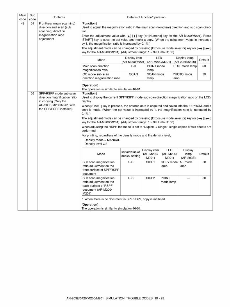
48 01 Front/rear (main scanning) direction and scan (sub scanning) direction magnification ratio adjustment
[Function]Used to adjust the magnification ratio in the main scan (front/rear) direction and sub scan direc-tion.
Enter the adjustment value with [ ] [ ] key (or [Numeric] key for the AR-M200/M201). Press[START] key to save the set value and make a copy. (When the adjustment value is increasedby 1, the magnification ratio is increased by 0.1%.)
The adjustment mode can be changed by pressing [Exposure mode selector] key (or [ ] [ ]key for the AR-M200/M201). (Adjustment range: 1 – 99, Default: 50)
[Operation]The operation is similar to simulation 46-01.
05 SPF/RSPF mode sub scan direction magnification ratio in copying (Only the AR-203E/M200/M201 with the SPF/RSPF installed)
[Function]Used to display the current SPF/RSPF mode sub scan direction magnification ratio on the LCD/display.
When [START] key is pressed, the entered data is acquired and saved into the EEPROM, and acopy is made. (When the set value is increased by 1, the magnification ratio is increased by0.1%.)
The adjustment mode can be changed by pressing [Exposure mode selector] key (or [ ] [ ]key for the AR-M200/M201). (Adjustment range: 1 – 99, Default: 50)
When adjusting the RSPF, the mode is set to "Duplex → Single," single copies of two sheets areperformed.
For printing, regardless of the density mode and the density level,
Density mode = MANUALDensity level = 3
* When there is no document in SPF/RSPF, copy is inhibited.
[Operation]The operation is similar to simulation 46-01.
Main code
Sub code
Contents Details of function/operation
ModeDisplay item
(AR-M200/M201)LED
(AR-M200/M201)Display lamp
(AR-203E/5420)Default
Main scan direction magnification ratio
F-R PRINT mode lamp
TEXT mode lamp 50
OC mode sub scan direction magnification ratio
SCAN SCAN mode lamp
PHOTO mode lamp
50
ModeInitial value of duplex setting
Display item(AR-M200/
M201)
LED(AR-M200/
M201)
Display lamp
(AR-203E)Default
Sub scan magnification ratio adjustment on the front surface of SPF/RSPF document
S-S SIDE1 COPY mode lamp
AE mode lamp
50
Sub scan magnification ratio adjustment on the back surface of RSPF document (AR-M200/M201)
D-S SIDE2 PRINT mode lamp
— 50
AR-203E/5420/M200/M201 SIMULATION, TROUBLE CODES 10 - 25

49 01 Flash ROM program writing mode
[Function]When this simulation is executed, "d" is displayed on the display (or "DOWNLOAD MODE" isdisplayed on the LCD for the AR-M200/M201), the machine goes into the program writing modefrom PC to Flash ROM.
Use the writing tool on the PC and write the program.
During writing, the display shows as follows:
After completion of download, turn OFF/ON the power to reset.
In case of an error in download, the following message is displayed on the LCD. (AR-M200/M201)
To enter the download mode, there is a method to use key operations as well as to use a simu-lation. With the power OFF, press and hold [Clear All] key + [ ] key, turn on the power.
[Operation] (AR-M200/M201)
Main code
Sub code
Contents Details of function/operation
* "∗" in an error display indicates the error position.
StatusAR-M200/M201 AR-203E/5420
RemarkDisplay item Display
Pre-heat lamp
Ready lamp
Download data receiving RECEIVING "d" ON ON OFFLoader function transfer LOADER COPYING AR-M200/M201Date delete start FLASH ERASE "d" ON OFF ONData write (Boot section) BOOT WRITING "d" ON Blink OFFData write (Program section)
PROGRAM WRITING "d" ON Blink Blink
Data write (EEPROM) E2PROM WRITING AR-M200/M201Data write (LCD) LCD DATE WRITING AR-M200/M201During SUM CHECK FLASH ROM SUM
CHECK"d" ON ON ON
During BOOT SUM CHECK
BOOT SUM CHECK AR-M200/M201
During EEPROM SUM CHECK
EEPROM SUM CHECK AR-M200/M201
Download complete DOWNLOAD COMPLETE!
"0FF" ON OFF OFF
Error state "E ∗" ON OFF OFF AR-203E/5420
1 Data reception error 6 Sum check (Loader section)2 Loader function transfer 7 Sum check (Boot section)3 FLASH ROM delete 8 Sum check (Program section)4 FLASH ROM writing (Boot section) 9 Sum check (EEPROM section)5 FLASH ROM writing (Program section) 10 Data error
Error status Display itemPC data receiving E-01 PC TRANSLoader function transfer E-02 LOADER COPYFLASH ROM delete E-03 FLASH ERASEBoot section FLASH ROM write E-04 BOOT WRITEProgram section FLASH ROM write E-05 PROGRAM WRITELoader section SUM CHECK E-06 LOADER SUMBoot section SUM CHECK E-07 BOOT SUMProgram section SUM CHECK E-08 PROGRAM SUME2PROM SUM CHECK E-09 E2PROM SUME2PROM write E-10 E2PROM WRITEE2PROM read Verify E-11 E2PROM READE2PROM collating Verify E-12 E2PROM COLLATEBoot section lens check E-13 BOOT LENGTHProgram section lens check E-14 PROGRAM LENGTHE2PROM lens check E-15 E2PROM LENGTHTotal data size check E-16 DATE SIZEIMC communication error E-17 IMC TRANSIMC FRASH ROM write E-18 IMC FLASH WRITELCD section lens check E-19 LCD DATE LENGTHLCD section FLASH ROM write E-20 LCD DATE WRITELCD section SUM CHECK E-21 LCD DATE SUM
1) Initial display
DOWNLOAD MODE
AR-203E/5420/M200/M201 SIMULATION, TROUBLE CODES 10 - 26
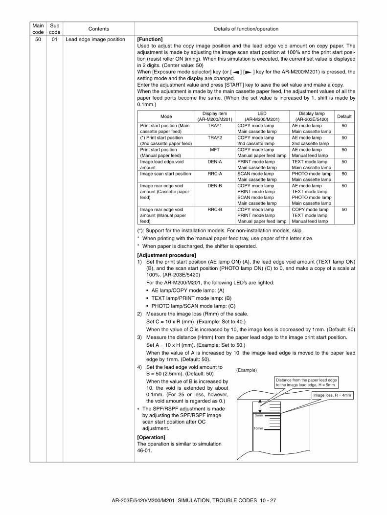
50 01 Lead edge image position [Function]Used to adjust the copy image position and the lead edge void amount on copy paper. Theadjustment is made by adjusting the image scan start position at 100% and the print start posi-tion (resist roller ON timing). When this simulation is executed, the current set value is displayedin 2 digits. (Center value: 50)When [Exposure mode selector] key (or [ ] [ ] key for the AR-M200/M201) is pressed, thesetting mode and the display are changed.Enter the adjustment value and press [START] key to save the set value and make a copy.When the adjustment is made by the main cassette paper feed, the adjustment values of all thepaper feed ports become the same. (When the set value is increased by 1, shift is made by0.1mm.)
(*): Support for the installation models. For non-installation models, skip.
* When printing with the manual paper feed tray, use paper of the letter size.
* When paper is discharged, the shifter is operated.
[Adjustment procedure]1) Set the print start position (AE lamp ON) (A), the lead edge void amount (TEXT lamp ON)
(B), and the scan start position (PHOTO lamp ON) (C) to 0, and make a copy of a scale at100%. (AR-203E/5420)
For the AR-M200/M201, the following LED’s are lighted:
• AE lamp/COPY mode lamp: (A)
• TEXT lamp/PRINT mode lamp: (B)
• PHOTO lamp/SCAN mode lamp: (C)
2) Measure the image loss (Rmm) of the scale.
Set C = 10 x R (mm). (Example: Set to 40.)
When the value of C is increased by 10, the image loss is decreased by 1mm. (Default: 50)
3) Measure the distance (Hmm) from the paper lead edge to the image print start position.
Set A = 10 x H (mm). (Example: Set to 50.)
When the value of A is increased by 10, the image lead edge is moved to the paper leadedge by 1mm. (Default: 50).
4) Set the lead edge void amount to B = 50 (2.5mm). (Default: 50)
When the value of B is increased by10, the void is extended by about0.1mm. (For 25 or less, however,the void amount is regarded as 0.)
∗ The SPF/RSPF adjustment is made by adjusting the SPF/RSPF image scan start position after OC adjustment.
[Operation]The operation is similar to simulation 46-01.
Main code
Sub code
Contents Details of function/operation
ModeDisplay item
(AR-M200/M201)LED
(AR-M200/M201)Display lamp
(AR-203E/5420)Default
Print start position (Main cassette paper feed)
TRAY1 COPY mode lampMain cassette lamp
AE mode lampMain cassette lamp
50
(*) Print start position (2nd cassette paper feed)
TRAY2 COPY mode lamp2nd cassette lamp
AE mode lamp2nd cassette lamp
50
Print start position (Manual paper feed)
MFT COPY mode lampManual paper feed lamp
AE mode lampManual feed lamp
50
Image lead edge void amount
DEN-A PRINT mode lampMain cassette lamp
TEXT mode lampMain cassette lamp
50
Image scan start position RRC-A SCAN mode lampMain cassette lamp
PHOTO mode lampMain cassette lamp
50
Image rear edge void amount (Cassette paper feed)
DEN-B COPY mode lampPRINT mode lampSCAN mode lampMain cassette lamp
AE mode lampTEXT mode lampPHOTO mode lampMain cassette lamp
50
Image rear edge void amount (Manual paper feed)
RRC-B COPY mode lampPRINT mode lampManual paper feed lamp
COPY mode lampTEXT mode lampManual feed lamp
50
5mm
10mm
Distance from the paper lead edge to the image lead edge, H = 5mm
Image loss, R = 4mm
(Example)
AR-203E/5420/M200/M201 SIMULATION, TROUBLE CODES 10 - 27
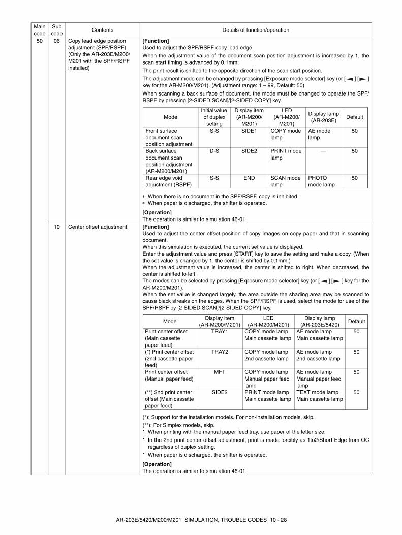
50 06 Copy lead edge position adjustment (SPF/RSPF) (Only the AR-203E/M200/M201 with the SPF/RSPF installed)
[Function]Used to adjust the SPF/RSPF copy lead edge.
When the adjustment value of the document scan position adjustment is increased by 1, thescan start timing is advanced by 0.1mm.
The print result is shifted to the opposite direction of the scan start position.
The adjustment mode can be changed by pressing [Exposure mode selector] key (or [ ] [ ]key for the AR-M200/M201). (Adjustment range: 1 – 99, Default: 50)
When scanning a back surface of document, the mode must be changed to operate the SPF/RSPF by pressing [2-SIDED SCAN]/[2-SIDED COPY] key.
∗ When there is no document in the SPF/RSPF, copy is inhibited.∗ When paper is discharged, the shifter is operated.
[Operation]The operation is similar to simulation 46-01.
10 Center offset adjustment [Function]Used to adjust the center offset position of copy images on copy paper and that in scanningdocument.When this simulation is executed, the current set value is displayed.Enter the adjustment value and press [START] key to save the setting and make a copy. (Whenthe set value is changed by 1, the center is shifted by 0.1mm.)When the adjustment value is increased, the center is shifted to right. When decreased, thecenter is shifted to left.The modes can be selected by pressing [Exposure mode selector] key (or [ ] [ ] key for theAR-M200/M201).When the set value is changed largely, the area outside the shading area may be scanned tocause black streaks on the edges. When the SPF/RSPF is used, select the mode for use of theSPF/RSPF by [2-SIDED SCAN]/[2-SIDED COPY] key.
(*): Support for the installation models. For non-installation models, skip.
(**): For Simplex models, skip.* When printing with the manual paper feed tray, use paper of the letter size.
* In the 2nd print center offset adjustment, print is made forcibly as 1to2/Short Edge from OCregardless of duplex setting.
* When paper is discharged, the shifter is operated.
[Operation]The operation is similar to simulation 46-01.
Main code
Sub code
Contents Details of function/operation
ModeInitial value of duplex setting
Display item (AR-M200/
M201)
LED(AR-M200/
M201)
Display lamp(AR-203E)
Default
Front surface document scan position adjustment
S-S SIDE1 COPY mode lamp
AE mode lamp
50
Back surface document scan position adjustment (AR-M200/M201)
D-S SIDE2 PRINT mode lamp
— 50
Rear edge void adjustment (RSPF)
S-S END SCAN mode lamp
PHOTO mode lamp
50
ModeDisplay item
(AR-M200/M201)LED
(AR-M200/M201)Display lamp
(AR-203E/5420)Default
Print center offset (Main cassette paper feed)
TRAY1 COPY mode lampMain cassette lamp
AE mode lampMain cassette lamp
50
(*) Print center offset (2nd cassette paper feed)
TRAY2 COPY mode lamp2nd cassette lamp
AE mode lamp2nd cassette lamp
50
Print center offset (Manual paper feed)
MFT COPY mode lampManual paper feed lamp
AE mode lampManual paper feed lamp
50
(**) 2nd print center offset (Main cassette paper feed)
SIDE2 PRINT mode lampMain cassette lamp
TEXT mode lampMain cassette lamp
50
AR-203E/5420/M200/M201 SIMULATION, TROUBLE CODES 10 - 28
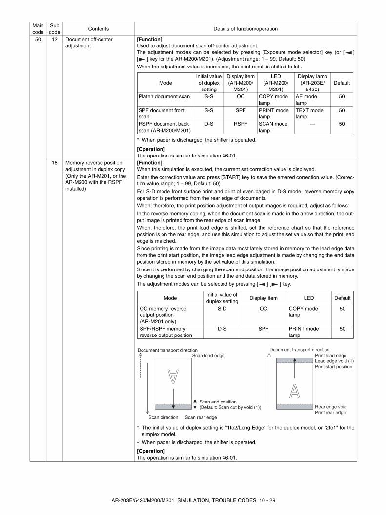
50 12 Document off-center adjustment
[Function]Used to adjust document scan off-center adjustment.The adjustment modes can be selected by pressing [Exposure mode selector] key (or [ ][ ] key for the AR-M200/M201). (Adjustment range: 1 – 99, Default: 50)
When the adjustment value is increased, the print result is shifted to left.
* When paper is discharged, the shifter is operated.
[Operation]The operation is similar to simulation 46-01.
18 Memory reverse position adjustment in duplex copy (Only the AR-M201, or the AR-M200 with the RSPF installed)
[Function]When this simulation is executed, the current set correction value is displayed.
Enter the correction value and press [START] key to save the entered correction value. (Correc-tion value range; 1 – 99, Default: 50)
For S-D mode front surface print and print of even paged in D-S mode, reverse memory copyoperation is performed from the rear edge of documents.
When, therefore, the print position adjustment of output images is required, adjust as follows:
In the reverse memory coping, when the document scan is made in the arrow direction, the out-put image is printed from the rear edge of scan image.
When, therefore, the print lead edge is shifted, set the reference chart so that the referenceposition is on the rear edge, and use this simulation to adjust the set value so that the print leadedge is matched.
Since printing is made from the image data most lately stored in memory to the lead edge datafrom the print start position, the image lead edge adjustment is made by changing the end dataposition stored in memory by the set value of this simulation.
Since it is performed by changing the scan end position, the image position adjustment is madeby changing the scan end position and the end data stored in memory.
The adjustment modes can be selected by pressing [ ] [ ] key.
* The initial value of duplex setting is "1to2/Long Edge" for the duplex model, or "2to1" for thesimplex model.
∗ When paper is discharged, the shifter is operated.
[Operation]The operation is similar to simulation 46-01.
Main code
Sub code
Contents Details of function/operation
ModeInitial value of duplex setting
Display item (AR-M200/
M201)
LED(AR-M200/
M201)
Display lamp (AR-203E/
5420)Default
Platen document scan S-S OC COPY mode lamp
AE mode lamp
50
SPF document front scan
S-S SPF PRINT mode lamp
TEXT mode lamp
50
RSPF document back scan (AR-M200/M201)
D-S RSPF SCAN mode lamp
— 50
ModeInitial value of duplex setting
Display item LED Default
OC memory reverse output position (AR-M201 only)
S-D OC COPY mode lamp
50
SPF/RSPF memory reverse output position
D-S SPF PRINT mode lamp
50
Document transport direction Document transport directionScan lead edge Print lead edge
Lead edge void (1)Print start position
Scan end position(Default: Scan cut by void (1)) Rear edge void
Print rear edgeScan direction Scan rear edge
AR-203E/5420/M200/M201 SIMULATION, TROUBLE CODES 10 - 29

50 19 Duplex copy rear edge void adjustment (AR-M201 only)
[Function]Used to adjust the rear edge void amount in duplex copy.
When this simulation is executed, the current set value is displayed in 2 digits. (Center value:50.) The adjustment modes can be selected by pressing [ ] [ ] key. (Adjustment range; 1 –99)
Enter the adjustment value and press [START] key to save the set value and make a copy. (Thepaper information is cleared for every copy.)
When the set value is increased by 1, the void amount is increased by about 0.1mm.
* The initial value for duplex setting is "1to2/Short Edge" for the OC setting, or "2to2" for theRSPF setting.
∗ When paper is discharged, the shifter is operated.
[Operation]The operation is similar to simulation 46-01.
51 02 Resist quantity adjustment [Function]Used to adjust the contact pressure of the main unit resist roller and the SPF/RSPF resist rolleronto paper. When this simulation is executed, the current set value is displayed.
The adjustment modes can be selected by pressing [Exposure mode selector] key (or [ ][ ] key for the AR-M200/M201).
Enter the adjustment value with [ ] [ ] key (or [Numeric] key for the AR-M200/M201) andpress [START] key to save the set value and make a copy.
(*): Support for the installation models. For non-installation models, skip.
[Operation] (AR-M200/M201)The operation is similar to simulation 46-01.
Main code
Sub code
Contents Details of function/operation
Mode Display item LED DefaultPaper rear edge void amount DEN-B PRINT mode lamp 50Print start position (Duplex back surface) RRC-D SCAN mode lamp 50
ModeDisplay item
(AR-M200/M201)LED
(AR-M200/M201)Display lamp
(AR-203E/5420)Default
Main cassette paper feed
TRAY1 COPY mode lampMain cassette lamp
AE mode lampMain cassette lamp
50
(*) 2nd cassette paper feed
TRAY2 COPY mode lamp2nd cassette lamp
AE mode lamp2nd cassette lamp
50
Manual paper feed MFT COPY mode lampManual paper feed lamp
AE mode lampManual paper feed lamp
50
RSPF document paper feed (Front surface) (AR-M200/M201)
SIDE1 COPY mode lampPRINT mode lampSCAN mode lampMain cassette lamp
— 50
RSPF document paper feed (Back surface) (AR-M200/M201)
SIDE2 COPY mode lampPRINT mode lampMain cassette lamp
— 50
(*) Duplex back surface (AR-M201 only)
DUP-2 PRINT mode lampSCAN mode lampMain cassette lamp
TEXT mode lampPHOTO mode lampMain cassette lamp
50
AR-203E/5420/M200/M201 SIMULATION, TROUBLE CODES 10 - 30
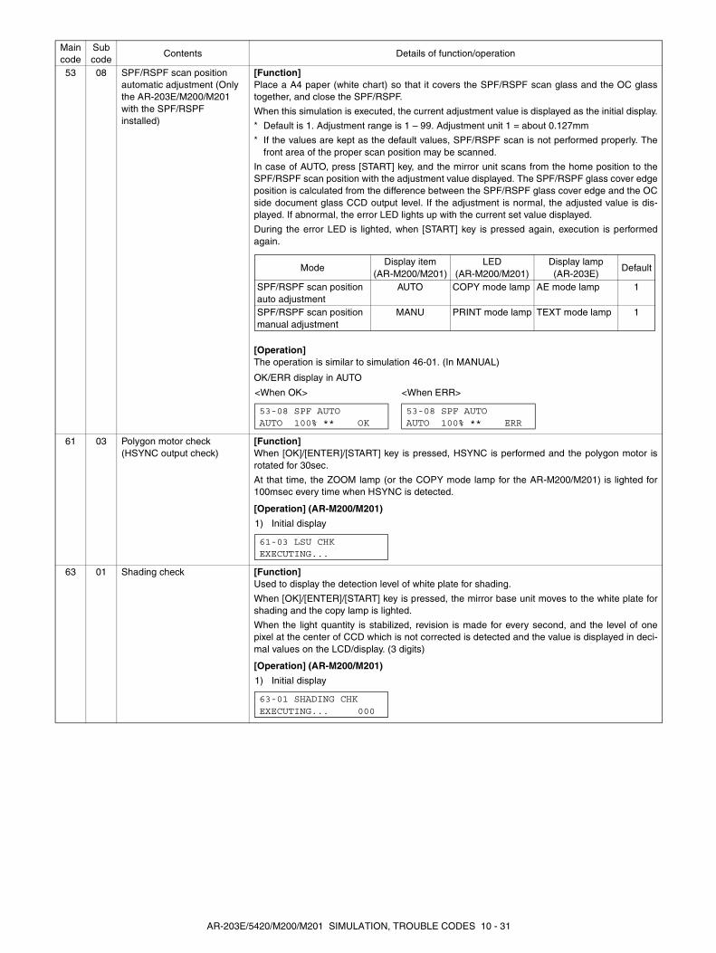
53 08 SPF/RSPF scan position automatic adjustment (Only the AR-203E/M200/M201 with the SPF/RSPF installed)
[Function]Place a A4 paper (white chart) so that it covers the SPF/RSPF scan glass and the OC glasstogether, and close the SPF/RSPF.
When this simulation is executed, the current adjustment value is displayed as the initial display.
* Default is 1. Adjustment range is 1 – 99. Adjustment unit 1 = about 0.127mm
* If the values are kept as the default values, SPF/RSPF scan is not performed properly. Thefront area of the proper scan position may be scanned.
In case of AUTO, press [START] key, and the mirror unit scans from the home position to theSPF/RSPF scan position with the adjustment value displayed. The SPF/RSPF glass cover edgeposition is calculated from the difference between the SPF/RSPF glass cover edge and the OCside document glass CCD output level. If the adjustment is normal, the adjusted value is dis-played. If abnormal, the error LED lights up with the current set value displayed.
During the error LED is lighted, when [START] key is pressed again, execution is performedagain.
[Operation]The operation is similar to simulation 46-01. (In MANUAL)
OK/ERR display in AUTO
61 03 Polygon motor check (HSYNC output check)
[Function]When [OK]/[ENTER]/[START] key is pressed, HSYNC is performed and the polygon motor isrotated for 30sec.
At that time, the ZOOM lamp (or the COPY mode lamp for the AR-M200/M201) is lighted for100msec every time when HSYNC is detected.
[Operation] (AR-M200/M201)
63 01 Shading check [Function]Used to display the detection level of white plate for shading.
When [OK]/[ENTER]/[START] key is pressed, the mirror base unit moves to the white plate forshading and the copy lamp is lighted.
When the light quantity is stabilized, revision is made for every second, and the level of onepixel at the center of CCD which is not corrected is detected and the value is displayed in deci-mal values on the LCD/display. (3 digits)
[Operation] (AR-M200/M201)
Main code
Sub code
Contents Details of function/operation
ModeDisplay item
(AR-M200/M201)LED
(AR-M200/M201)Display lamp(AR-203E)
Default
SPF/RSPF scan position auto adjustment
AUTO COPY mode lamp AE mode lamp 1
SPF/RSPF scan position manual adjustment
MANU PRINT mode lamp TEXT mode lamp 1
<When OK> <When ERR>
53-08 SPF AUTOAUTO 100% ** OK
53-08 SPF AUTOAUTO 100% ** ERR
1) Initial display
61-03 LSU CHKEXECUTING...
1) Initial display
63-01 SHADING CHKEXECUTING... 000
AR-203E/5420/M200/M201 SIMULATION, TROUBLE CODES 10 - 31
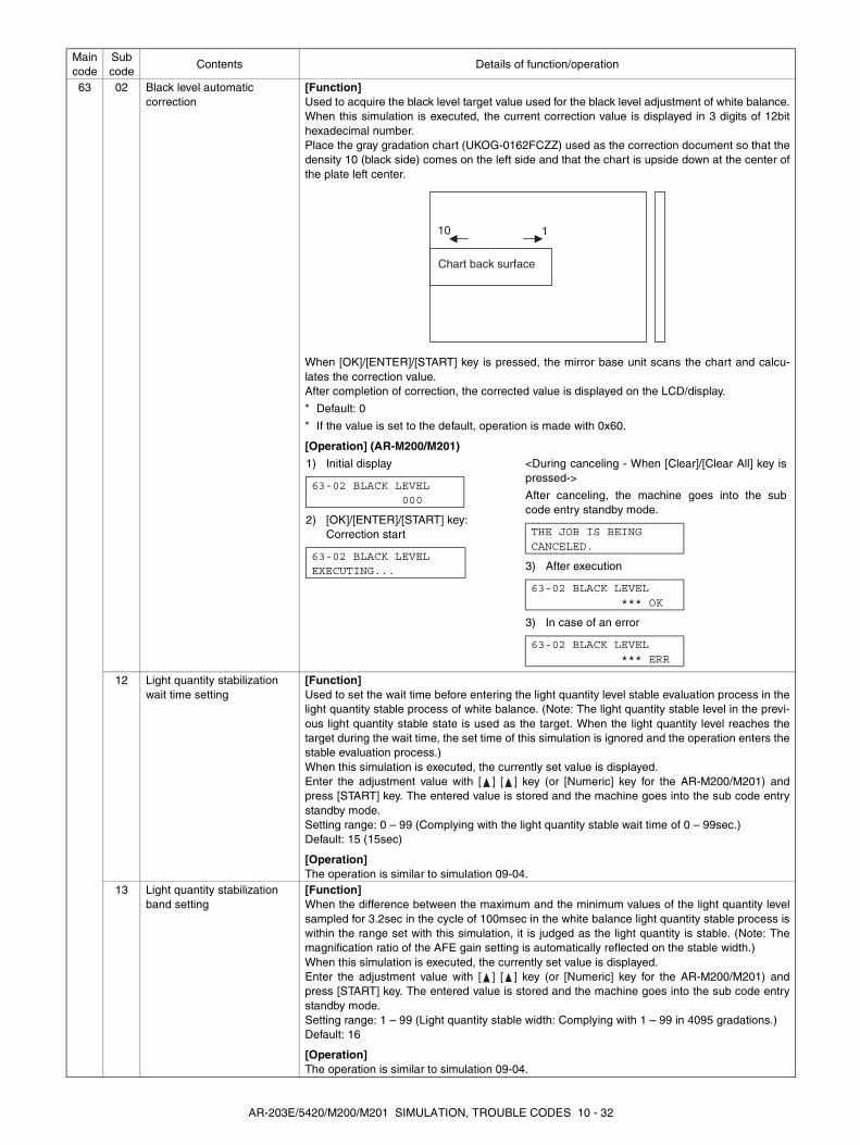
63 02 Black level automatic correction
[Function]Used to acquire the black level target value used for the black level adjustment of white balance.When this simulation is executed, the current correction value is displayed in 3 digits of 12bithexadecimal number.Place the gray gradation chart (UKOG-0162FCZZ) used as the correction document so that thedensity 10 (black side) comes on the left side and that the chart is upside down at the center ofthe plate left center.
When [OK]/[ENTER]/[START] key is pressed, the mirror base unit scans the chart and calcu-lates the correction value.After completion of correction, the corrected value is displayed on the LCD/display.
* Default: 0
* If the value is set to the default, operation is made with 0x60.
[Operation] (AR-M200/M201)
12 Light quantity stabilization wait time setting
[Function]Used to set the wait time before entering the light quantity level stable evaluation process in thelight quantity stable process of white balance. (Note: The light quantity stable level in the previ-ous light quantity stable state is used as the target. When the light quantity level reaches thetarget during the wait time, the set time of this simulation is ignored and the operation enters thestable evaluation process.)When this simulation is executed, the currently set value is displayed.Enter the adjustment value with [ ] [ ] key (or [Numeric] key for the AR-M200/M201) andpress [START] key. The entered value is stored and the machine goes into the sub code entrystandby mode.Setting range: 0 – 99 (Complying with the light quantity stable wait time of 0 – 99sec.)Default: 15 (15sec)
[Operation]The operation is similar to simulation 09-04.
13 Light quantity stabilization band setting
[Function]When the difference between the maximum and the minimum values of the light quantity levelsampled for 3.2sec in the cycle of 100msec in the white balance light quantity stable process iswithin the range set with this simulation, it is judged as the light quantity is stable. (Note: Themagnification ratio of the AFE gain setting is automatically reflected on the stable width.)When this simulation is executed, the currently set value is displayed.Enter the adjustment value with [ ] [ ] key (or [Numeric] key for the AR-M200/M201) andpress [START] key. The entered value is stored and the machine goes into the sub code entrystandby mode.Setting range: 1 – 99 (Light quantity stable width: Complying with 1 – 99 in 4095 gradations.)Default: 16
[Operation]The operation is similar to simulation 09-04.
Main code
Sub code
Contents Details of function/operation
Chart back surface
10
1) Initial display
2) [OK]/[ENTER]/[START] key: Correction start
63-02 BLACK LEVEL 000
63-02 BLACK LEVELEXECUTING...
<During canceling - When [Clear]/[Clear All] key ispressed->
After canceling, the machine goes into the subcode entry standby mode.
3) After execution
3) In case of an error
THE JOB IS BEINGCANCELED.
63-02 BLACK LEVEL *** OK
63-02 BLACK LEVEL *** ERR
AR-203E/5420/M200/M201 SIMULATION, TROUBLE CODES 10 - 32
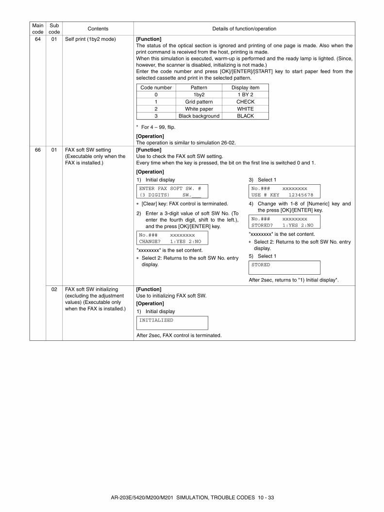
64 01 Self print (1by2 mode) [Function]The status of the optical section is ignored and printing of one page is made. Also when theprint command is received from the host, printing is made.When this simulation is executed, warm-up is performed and the ready lamp is lighted. (Since,however, the scanner is disabled, initializing is not made.)Enter the code number and press [OK]/[ENTER]/[START] key to start paper feed from theselected cassette and print in the selected pattern.
* For 4 – 99, flip.
[Operation]The operation is similar to simulation 26-02.
66 01 FAX soft SW setting (Executable only when the FAX is installed.)
[Function]Use to check the FAX soft SW setting.Every time when the key is pressed, the bit on the first line is switched 0 and 1.
[Operation]
02 FAX soft SW initializing (excluding the adjustment values) (Executable only when the FAX is installed.)
[Function]Use to initializing FAX soft SW.
[Operation]
Main code
Sub code
Contents Details of function/operation
Code number Pattern Display item0 1by2 1 BY 21 Grid pattern CHECK2 White paper WHITE3 Black background BLACK
1) Initial display
∗ [Clear] key: FAX control is terminated.
2) Enter a 3-digit value of soft SW No. (Toenter the fourth digit, shift to the left.),and the press [OK]/[ENTER] key.
"xxxxxxxx" is the set content.
∗ Select 2: Returns to the soft SW No. entrydisplay.
3) Select 1
4) Change with 1-8 of [Numeric] key andthe press [OK]/[ENTER] key.
"xxxxxxxx" is the set content.
∗ Select 2: Returns to the soft SW No. entrydisplay.
5) Select 1
After 2sec, returns to "1) Initial display".
ENTER FAX SOFT SW. #(3 DIGITS) SW.___
No.### xxxxxxxxCHANGE? 1:YES 2:NO
No.### xxxxxxxxUSE # KEY 12345678
No.### xxxxxxxxSTORED? 1:YES 2:NO
STORED
1) Initial display
After 2sec, FAX control is terminated.
INITIALIZED
AR-203E/5420/M200/M201 SIMULATION, TROUBLE CODES 10 - 33
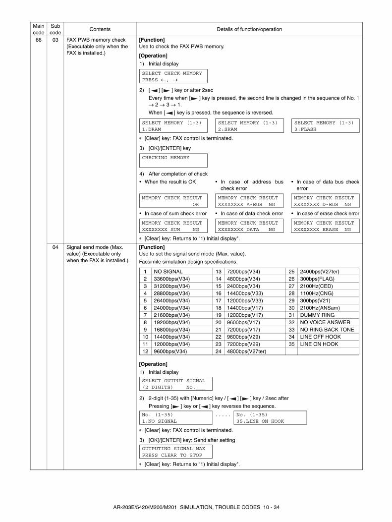
66 03 FAX PWB memory check (Executable only when the FAX is installed.)
[Function]Use to check the FAX PWB memory.
[Operation]
04 Signal send mode (Max. value) (Executable only when the FAX is installed.)
[Function]Use to set the signal send mode (Max. value).
Facsimile simulation design specifications.
[Operation]
Main code
Sub code
Contents Details of function/operation
1) Initial display
2) [ ] [ ] key or after 2sec
Every time when [ ] key is pressed, the second line is changed in the sequence of No. 1→ 2 → 3 → 1.
When [ ] key is pressed, the sequence is reversed.
∗ [Clear] key: FAX control is terminated.
3) [OK]/[ENTER] key
4) After completion of check
• When the result is OK
• In case of sum check error
• In case of address buscheck error
• In case of data check error
• In case of data bus checkerror
• In case of erase check error
∗ [Clear] key: Returns to "1) Initial display".
SELECT CHECK MEMORYPRESS ←, →
SELECT MEMORY (1-3)1:DRAM
SELECT MEMORY (1-3)2:SRAM
SELECT MEMORY (1-3)3:FLASH
CHECKING MEMORY
MEMORY CHECK RESULT OK
MEMORY CHECK RESULTXXXXXXXX SUM NG
MEMORY CHECK RESULTXXXXXXXX A-BUS NG
MEMORY CHECK RESULTXXXXXXXX DATA NG
MEMORY CHECK RESULTXXXXXXXX D-BUS NG
MEMORY CHECK RESULTXXXXXXXX ERASE NG
1 NO SIGNAL 13 7200bps(V34) 25 2400bps(V27ter)2 33600bps(V34) 14 4800bps(V34) 26 300bps(FLAG)3 31200bps(V34) 15 2400bps(V34) 27 2100Hz(CED)4 28800bps(V34) 16 14400bps(V33) 28 1100Hz(CNG)5 26400bps(V34) 17 12000bps(V33) 29 300bps(V21)6 24000bps(V34) 18 14400bps(V17) 30 2100Hz(ANSam)7 21600bps(V34) 19 12000bps(V17) 31 DUMMY RING8 19200bps(V34) 20 9600bps(V17) 32 NO VOICE ANSWER9 16800bps(V34) 21 7200bps(V17) 33 NO RING BACK TONE10 14400bps(V34) 22 9600bps(V29) 34 LINE OFF HOOK11 12000bps(V34) 23 7200bps(V29) 35 LINE ON HOOK12 9600bps(V34) 24 4800bps(V27ter)
1) Initial display
2) 2-digit (1-35) with [Numeric] key / [ ] [ ] key / 2sec after
Pressing [ ] key or [ ] key reverses the sequence.
∗ [Clear] key: FAX control is terminated.
3) [OK]/[ENTER] key: Send after setting
∗ [Clear] key: Returns to "1) Initial display".
SELECT OUTPUT SIGNAL(2 DIGITS) No.___
No. (1-35)1:NO SIGNAL
..... No. (1-35)35:LINE ON HOOK
OUTPUTING SIGNAL MAXPRESS CLEAR TO STOP
AR-203E/5420/M200/M201 SIMULATION, TROUBLE CODES 10 - 34
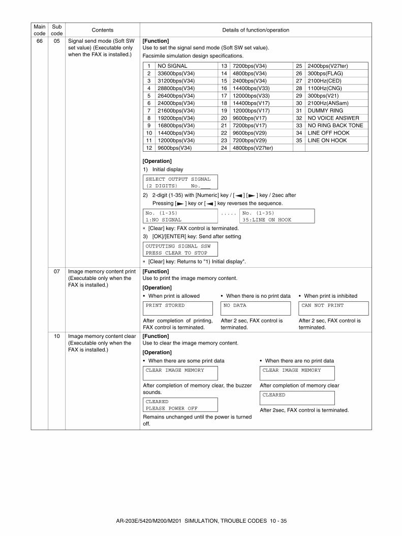
66 05 Signal send mode (Soft SW set value) (Executable only when the FAX is installed.)
[Function]Use to set the signal send mode (Soft SW set value).
Facsimile simulation design specifications.
[Operation]
07 Image memory content print (Executable only when the FAX is installed.)
[Function]Use to print the image memory content.
[Operation]
10 Image memory content clear (Executable only when the FAX is installed.)
[Function]Use to clear the image memory content.
[Operation]
Main code
Sub code
Contents Details of function/operation
1 NO SIGNAL 13 7200bps(V34) 25 2400bps(V27ter)2 33600bps(V34) 14 4800bps(V34) 26 300bps(FLAG)3 31200bps(V34) 15 2400bps(V34) 27 2100Hz(CED)4 28800bps(V34) 16 14400bps(V33) 28 1100Hz(CNG)5 26400bps(V34) 17 12000bps(V33) 29 300bps(V21)6 24000bps(V34) 18 14400bps(V17) 30 2100Hz(ANSam)7 21600bps(V34) 19 12000bps(V17) 31 DUMMY RING8 19200bps(V34) 20 9600bps(V17) 32 NO VOICE ANSWER9 16800bps(V34) 21 7200bps(V17) 33 NO RING BACK TONE10 14400bps(V34) 22 9600bps(V29) 34 LINE OFF HOOK11 12000bps(V34) 23 7200bps(V29) 35 LINE ON HOOK12 9600bps(V34) 24 4800bps(V27ter)
1) Initial display
2) 2-digit (1-35) with [Numeric] key / [ ] [ ] key / 2sec after
Pressing [ ] key or [ ] key reverses the sequence.
∗ [Clear] key: FAX control is terminated.
3) [OK]/[ENTER] key: Send after setting
∗ [Clear] key: Returns to "1) Initial display".
SELECT OUTPUT SIGNAL(2 DIGITS) No.___
No. (1-35)1:NO SIGNAL
..... No. (1-35)35:LINE ON HOOK
OUTPUTING SIGNAL SSWPRESS CLEAR TO STOP
• When print is allowed
After completion of printing,FAX control is terminated.
• When there is no print data
After 2 sec, FAX control is terminated.
• When print is inhibited
After 2 sec, FAX control is terminated.
PRINT STORED NO DATA CAN NOT PRINT
• When there are some print data
After completion of memory clear, the buzzersounds.
Remains unchanged until the power is turnedoff.
• When there are no print data
After completion of memory clear
After 2sec, FAX control is terminated.
CLEAR IMAGE MEMORY
CLEAREDPLEASE POWER OFF
CLEAR IMAGE MEMORY
CLEARED
AR-203E/5420/M200/M201 SIMULATION, TROUBLE CODES 10 - 35
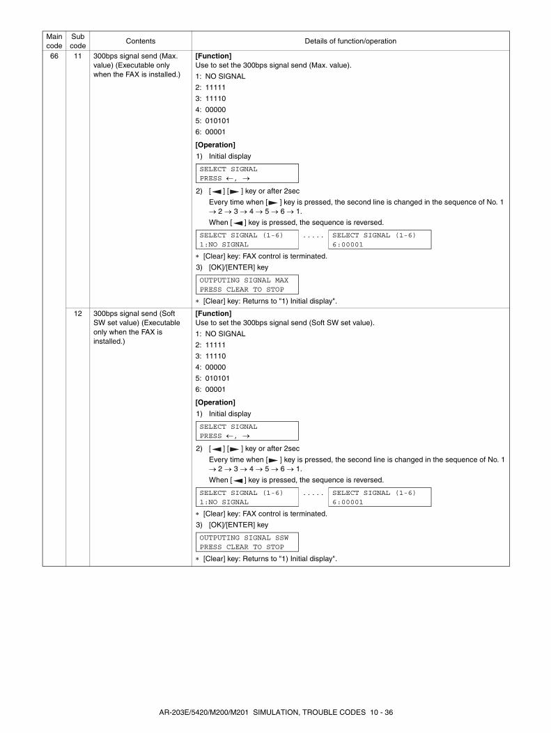
66 11 300bps signal send (Max. value) (Executable only when the FAX is installed.)
[Function]Use to set the 300bps signal send (Max. value).
1: NO SIGNAL
2: 11111
3: 11110
4: 00000
5: 010101
6: 00001
[Operation]
12 300bps signal send (Soft SW set value) (Executable only when the FAX is installed.)
[Function]Use to set the 300bps signal send (Soft SW set value).
1: NO SIGNAL
2: 11111
3: 11110
4: 00000
5: 010101
6: 00001
[Operation]
Main code
Sub code
Contents Details of function/operation
1) Initial display
2) [ ] [ ] key or after 2sec
Every time when [ ] key is pressed, the second line is changed in the sequence of No. 1→ 2 → 3 → 4 → 5 → 6 → 1.
When [ ] key is pressed, the sequence is reversed.
∗ [Clear] key: FAX control is terminated.
3) [OK]/[ENTER] key
∗ [Clear] key: Returns to "1) Initial display".
SELECT SIGNALPRESS ←, →
SELECT SIGNAL (1-6)1:NO SIGNAL
..... SELECT SIGNAL (1-6)6:00001
OUTPUTING SIGNAL MAXPRESS CLEAR TO STOP
1) Initial display
2) [ ] [ ] key or after 2sec
Every time when [ ] key is pressed, the second line is changed in the sequence of No. 1→ 2 → 3 → 4 → 5 → 6 → 1.
When [ ] key is pressed, the sequence is reversed.
∗ [Clear] key: FAX control is terminated.
3) [OK]/[ENTER] key
∗ [Clear] key: Returns to "1) Initial display".
SELECT SIGNALPRESS ←, →
SELECT SIGNAL (1-6)1:NO SIGNAL
..... SELECT SIGNAL (1-6)6:00001
OUTPUTING SIGNAL SSWPRESS CLEAR TO STOP
AR-203E/5420/M200/M201 SIMULATION, TROUBLE CODES 10 - 36
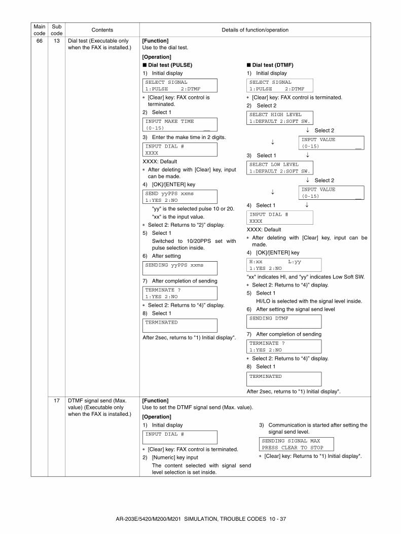
66 13 Dial test (Executable only when the FAX is installed.)
[Function]Use to the dial test.
[Operation]
17 DTMF signal send (Max. value) (Executable only when the FAX is installed.)
[Function]Use to set the DTMF signal send (Max. value).
[Operation]
Main code
Sub code
Contents Details of function/operation
Dial test (PULSE)
1) Initial display
∗ [Clear] key: FAX control is terminated.
2) Select 1
3) Enter the make time in 2 digits.
XXXX: Default
∗ After deleting with [Clear] key, inputcan be made.
4) [OK]/[ENTER] key
"yy" is the selected pulse 10 or 20.
"xx" is the input value.
∗ Select 2: Returns to “2)” display.
5) Select 1
Switched to 10/20PPS set withpulse selection inside.
6) After setting
7) After completion of sending
∗ Select 2: Returns to “4)” display.
8) Select 1
After 2sec, returns to "1) Initial display".
SELECT SIGNAL1:PULSE 2:DTMF
INPUT MAKE TIME(0-15) __
INPUT DIAL #XXXX
SEND yyPPS xxms1:YES 2:NO
SENDING yyPPS xxms
TERMINATE ?1:YES 2:NO
TERMINATED
Dial test (DTMF)
1) Initial display
∗ [Clear] key: FAX control is terminated.
2) Select 2
↓ Select 2
3) Select 1 ↓
↓ Select 2
4) Select 1 ↓
XXXX: Default
∗ After deleting with [Clear] key, input can bemade.
4) [OK]/[ENTER] key
"xx" indicates HI, and "yy" indicates Low Soft SW.
∗ Select 2: Returns to “4)” display.
5) Select 1
HI/LO is selected with the signal level inside.
6) After setting the signal send level
7) After completion of sending
∗ Select 2: Returns to “4)” display.
8) Select 1
After 2sec, returns to "1) Initial display".
SELECT SIGNAL1:PULSE 2:DTMF
SELECT HIGH LEVEL1:DEFAULT 2:SOFT SW.
↓INPUT VALUE(0-15) __
SELECT LOW LEVEL1:DEFAULT 2:SOFT SW.
↓INPUT VALUE(0-15) __
INPUT DIAL #XXXX
H:xx L:yy1:YES 2:NO
SENDING DTMF
TERMINATE ?1:YES 2:NO
TERMINATED
1) Initial display
∗ [Clear] key: FAX control is terminated.
2) [Numeric] key input
The content selected with signal sendlevel selection is set inside.
3) Communication is started after setting thesignal send level.
∗ [Clear] key: Returns to "1) Initial display".
INPUT DIAL #SENDING SIGNAL MAXPRESS CLEAR TO STOP
AR-203E
/5420/M200/M201 SIMULATION, TROUBL E CODES 10 - 37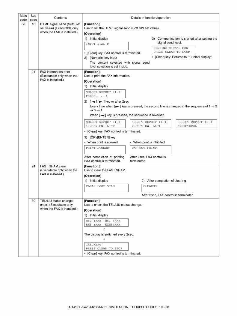
66 18 DTMF signal send (Soft SW set value) (Executable only when the FAX is installed.)
[Function]Use to set the DTMF signal send (Soft SW set value).
[Operation]
21 FAX information print (Executable only when the FAX is installed.)
[Function]Use to print the FAX information.
[Operation]
24 FAST SRAM clear (Executable only when the FAX is installed.)
[Function]Use to clear the FAST SRAM.
[Operation]
30 TEL/LIU status change check (Executable only when the FAX is installed.)
[Function]Use to check the TEL/LIU status change.
[Operation]
Main code
Sub code
Contents Details of function/operation
1) Initial display
∗ [Clear] key: FAX control is terminated.
2) [Numeric] key input
The content selected with signal sendlevel selection is set inside.
3) Communication is started after setting thesignal send level.
∗ [Clear] key: Returns to "1) Initial display".
INPUT DIAL #SENDING SIGNAL SSWPRESS CLEAR TO STOP
1) Initial display
2) [ ] [ ] key or after 2sec
Every time when [ ] key is pressed, the second line is changed in the sequence of 1 → 2→ 3 → 1.
When [ ] key is pressed, the sequence is reversed.
∗ [Clear] key: FAX control is terminated.
3) [OK]/[ENTER] key
• When print is allowed
After completion of printing,FAX control is terminated.
• When print is inhibited
After 2sec, FAX control is terminated.
SELECT REPORT (1-3)PRESS ←, →
SELECT REPORT (1-3)1:USER SW. LIST
SELECT REPORT (1-3)2:SOFT SW. LIST
SELECT REPORT (1-3)3:PROTOCOL
PRINT STORED CAN NOT PRINT
1) Initial display 2) After completion of clearing
After 2sec, FAX control is terminated.
CLEAR FAST SRAM CLEARED
1) Initial display
↑
The display is switched every 2sec.
↓
∗ [Clear] key: FAX control is terminated.
HS2 :xxx HS1 :xxxRHS :xxx EXHS:xxx
CHECKINGPRESS CLEAR TO STOP
AR-203E/5420/M200/M201 SIMULATION, TROUBLE CODES 10 - 38

66 33 Signal detection check (Executable only when the FAX is installed.)
[Function]Use to check the signal detection.
[Operation]
34 Communication time measurement (Executable only when the FAX is installed.)
[Function]Use to measurement the communication time.
[Operation]
37 Speaker sound volume setting (Executable only when the FAX is installed.)
[Function]Use to set the speaker sound volume.
1: NO SOUND2: LOW3: MID4: HIGH
[Operation]
Main code
Sub code
Contents Details of function/operation
1) Initial display
When a signal is detected, the display is changed from NONE to the following.
CI/CNG/CED/BT/DT/Flag/SDT/DTMF
∗ [Clear] key: FAX control is terminated.
CHECKING NONEPRESS CLEAR TO STOP
1) Initial display
"xx:xx:xx:xxx" indicates o'clock, minute, second, millisecond.
∗ [Clear] key: FAX control is terminated.
COMM. TIMExx:xx:xx:xxx msec
1) Initial display
2) [ ] [ ] key or after 2sec
Every time when [ ] key is pressed, the second line is changed in the sequence of 1 → 2→ 3 → 4 → 1.
When [ ] key is pressed, the sequence is reversed.
∗ [Clear] key: FAX control is terminated.
3) [OK]/[ENTER] key
xxx: Set content
After 2sec, FAX control is terminated.
SELECT SPEEKER VOL.PRESS ←, →
SELECT (1-4)1:NO SOUND
SELECT (1-4)2:LOW
.....
STOREDxxx
AR-203E/5420/M200/M201 SIMULATION, TROUBLE CODES 10 - 39
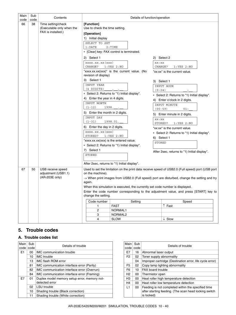
5. Trouble codesA. Trouble codes list
66 38 Time setting/check (Executable only when the FAX is installed.)
[Function]Use to check the time setting.
[Operation]
67 50 USB receive speed adjustment (USB1.1) (AR-203E only)
Used to set the limitation on the print data receive speed of USB2.0 (Full speed) port (USB porton the machine).
→ When print images from USB2.0 (Full speed) port are disturbed, change the setting and tryagain.
When this simulation is executed, the currently set code number is displayed.
Enter the code number corresponding to the adjustment value, and press [START] key tochange the setting.
Main code
Sub code
Contents Details of function/operation
1) Initial display
∗ [Clear] key: FAX control is terminated.
2) Select 1
"xxxx.xx.xx(xxx)" is the current value. (Norevision of display)
3) Select 1
∗ Select 2: Returns to "1) Initial display".
4) Enter the year in 4 digits.
5) Enter the month in 2 digits.
6) Enter the day in 2 digits.
"xxxx.xx.xx(xxx) is the entered value.
∗ Select 2: Returns to "1) Initial display".
7) Select 1
After 2sec, returns to "1) Initial display".
2) Select 2
"xx:xx" is the current value.
3) Select 1
∗ Select 2: Returns to "1) Initial display".
4) Enter o'clock in 2 digits.
5) Enter minute in 2 digits.
"xx:xx" is the current value.
∗ Select 2: Returns to "1) Initial display".
6) Select 1
After 2sec, returns to "1) Initial display".
SELECT TO SET1:DATE 2:TIME
xxxx.xx.xx(xxx)CHANGE? 1:YES 2:NO
INPUT YEAR(4 DIGITS)____.__.__
INPUT MONTH(1-12) 1998.__.__
INPUT DAY(1-31) 1998.01.__
xxxx.xx.xx(xxx)STORED? 1:YES 2:NO
STORED
xx:xxCHANGE? 1:YES 2:NO
INPUT HOUR(0-24) __:__
INPUT MINUTE(00-59) 01:__
xx:xxSTORED? 1:YES 2:NO
STORED
Code number Setting Speed1 FAST ↑ Fast2 NORMAL13 NORMAL24 SLOW ↓ Slow
Main code
Sub code
Details of trouble
E1 00 IMC communication trouble10 IMC trouble13 IMC flash ROM error81 IMC communication interface error (Parity)82 IMC communication interface error (Overrun)84 IMC communication interface error (Framing)
E7 01 Duplex model memory setup error, memory not-detected error
02 LSU trouble10 Shading trouble (Black correction)11 Shading trouble (White correction)
Main code
Sub code
Details of trouble
E7 16 Abnormal laser outputF2 02 Toner supply abnormality
04 Improper cartridge (Destination error, life cycle error)F5 02 Copy lamp lighting abnormalityF6 10 FAX board troubleH2 00 Thermistor openH3 00 Heat roller high temperature detectionH4 00 Heat roller low temperature detectionL1 00 Feeding is not completed within the specified time
after starting feeding. (The scan head locking switch is locked)
AR-203E/5420/M200/M201 SIMULATION, TROUBLE CODES 10 - 40
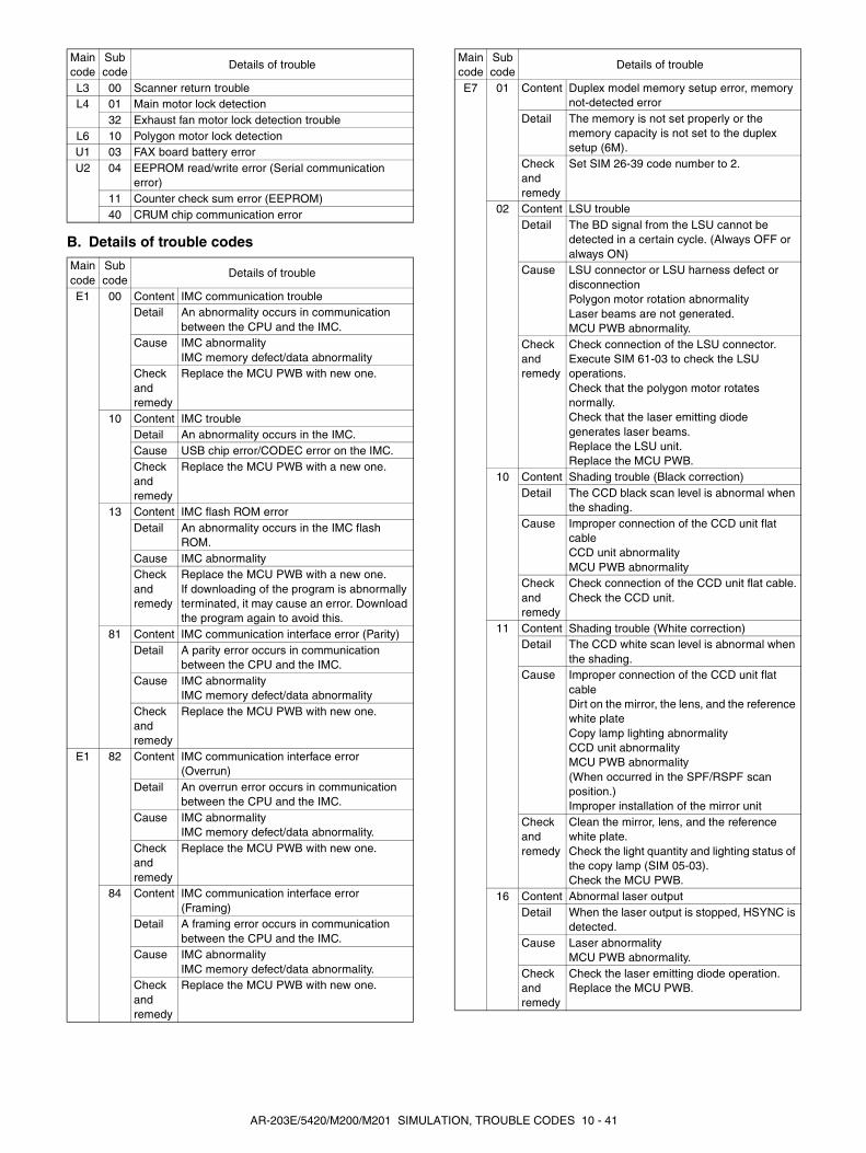
B. Details of trouble codes
L3 00 Scanner return troubleL4 01 Main motor lock detection
32 Exhaust fan motor lock detection troubleL6 10 Polygon motor lock detectionU1 03 FAX board battery errorU2 04 EEPROM read/write error (Serial communication
error)11 Counter check sum error (EEPROM)40 CRUM chip communication error
Main code
Sub code
Details of trouble
E1 00 Content IMC communication troubleDetail An abnormality occurs in communication
between the CPU and the IMC.Cause IMC abnormality
IMC memory defect/data abnormalityCheck and remedy
Replace the MCU PWB with new one.
10 Content IMC troubleDetail An abnormality occurs in the IMC.Cause USB chip error/CODEC error on the IMC.Check and remedy
Replace the MCU PWB with a new one.
13 Content IMC flash ROM errorDetail An abnormality occurs in the IMC flash
ROM.Cause IMC abnormalityCheck and remedy
Replace the MCU PWB with a new one.If downloading of the program is abnormally terminated, it may cause an error. Download the program again to avoid this.
81 Content IMC communication interface error (Parity)Detail A parity error occurs in communication
between the CPU and the IMC.Cause IMC abnormality
IMC memory defect/data abnormalityCheck and remedy
Replace the MCU PWB with new one.
E1 82 Content IMC communication interface error (Overrun)
Detail An overrun error occurs in communication between the CPU and the IMC.
Cause IMC abnormalityIMC memory defect/data abnormality.
Check and remedy
Replace the MCU PWB with new one.
84 Content IMC communication interface error (Framing)
Detail A framing error occurs in communication between the CPU and the IMC.
Cause IMC abnormalityIMC memory defect/data abnormality.
Check and remedy
Replace the MCU PWB with new one.
Main code
Sub code
Details of trouble
E7 01 Content Duplex model memory setup error, memory not-detected error
Detail The memory is not set properly or the memory capacity is not set to the duplex setup (6M).
Check and remedy
Set SIM 26-39 code number to 2.
02 Content LSU troubleDetail The BD signal from the LSU cannot be
detected in a certain cycle. (Always OFF or always ON)
Cause LSU connector or LSU harness defect or disconnectionPolygon motor rotation abnormalityLaser beams are not generated.MCU PWB abnormality.
Check and remedy
Check connection of the LSU connector.Execute SIM 61-03 to check the LSU operations.Check that the polygon motor rotates normally.Check that the laser emitting diode generates laser beams.Replace the LSU unit.Replace the MCU PWB.
10 Content Shading trouble (Black correction)Detail The CCD black scan level is abnormal when
the shading.Cause Improper connection of the CCD unit flat
cableCCD unit abnormalityMCU PWB abnormality
Check and remedy
Check connection of the CCD unit flat cable.Check the CCD unit.
11 Content Shading trouble (White correction)Detail The CCD white scan level is abnormal when
the shading.Cause Improper connection of the CCD unit flat
cableDirt on the mirror, the lens, and the reference white plateCopy lamp lighting abnormalityCCD unit abnormalityMCU PWB abnormality(When occurred in the SPF/RSPF scan position.)Improper installation of the mirror unit
Check and remedy
Clean the mirror, lens, and the reference white plate.Check the light quantity and lighting status of the copy lamp (SIM 05-03).Check the MCU PWB.
16 Content Abnormal laser outputDetail When the laser output is stopped, HSYNC is
detected.Cause Laser abnormality
MCU PWB abnormality.Check and remedy
Check the laser emitting diode operation.Replace the MCU PWB.
Main code
Sub code
Details of trouble
AR-203E/5420/M200/M201 SIMULATION, TROUBLE CODES 10 - 41
F2 02 Content Toner supply abnormalityDetail The maximum toner supply time is greatly
exceeded.Cause CRUM chip trouble
Improper developing unitCheck and remedy
Replace the CRUM chip.Replace the developing unit.
04 Content Improper cartridge (Destination error, life cycle error)
Detail The destination of the main unit differs from that of the CRUM.When the life cycle information is other than Not Used (FFh).
Cause CRUM chip troubleImproper developing unit
Check and remedy
Replace the CRUM chip.Replace the developing unit.
F5 02 Content Copy lamp lighting abnormalityDetail The copy lamp does not turn on.Cause Copy lamp abnormality
Copy lamp harness abnormalityCCD PWB harness abnormality.
Check and remedy
Use SIM 5-3 to check the copy lamp operations.When the copy lamp lights up.Check the harness and the connector between the CCD unit and the MCU PWB.When the copy lamp does not light up.Check the harness and the connector between the copy lamp unit and the MCU PWB.Replace the copy lamp unit.Replace the MCU PWB.
F6 10 Content FAX board troubleDetail Communication trouble between MCU and
FAX control PWBCause FAX control PWB connector disconnection
Defective harness between FAX control PWB and MCU PWBMotherboard connector pin breakageFAX control PWB ROM error/Data errorIC on FAX PWB causes abnormality
Check and remedy
Check connector/harness of FAX control PWB and MCU PWB.Check the grounding of the copier.Check FAX control PWB ROM.Replace the FAX PWB.
H2 00 Content Thermistor openDetail The thermistor is open.
The fusing unit is not installed.Cause Thermistor abnormality
Control PWB abnormalityFusing section connector disconnectionThe fusing unit is not installed.
Check and remedy
Check the harness and the connector between the thermistor and the PWB.Use SIM 14 to clear the self diagnostic display.
Main code
Sub code
Details of trouble
H3 00 Content Heat roller high temperature detectionDetail The fusing temperature exceeds 240°C.Cause Thermistor abnormality
Control PWB abnormalityFusing section connector disconnection.
Check and remedy
Use SIM 5-02 to check the heater lamp blinking operation.When the lamp blinks normally.Check the thermistor and its harness.Check the thermistor input circuit on the control PWB.When the lamp keeps ON.Check the power PWB and the lamp control circuit on the MCU PWB.Use SIM 14 to clear the self diagnostic display.
H4 00 Content Heat roller low temperature detectionDetail 1) When the target temperature (165°C) is
not reached in 55 sec after starting warming-up.
2) When the temperature below 100°C is detected for 300ms under the ready print state.
∗ "Starting warming-up" means not only that in power supply but also reset that in reset from shut-off and in side door close. (The timing of generating H4 is not limited to that in power supply.)
Cause Thermistor abnormalityHeater lamp abnormalityThermostat abnormalityControl PWB abnormality
Check and remedy
Use SIM 5-02 to check the heater lamp blinking operation.When the lamp blinks normally.Check the thermistor and its harness.Check the thermistor input circuit on the control PWB.When the lamp does not light up.Check for disconnection of the heater lamp and the thermostat. Check the interlock switch.Check the power PWB and the lamp control circuit on the MCU PWB.Use SIM 14 to clear the self diagnostic display.
Main code
Sub code
Details of trouble
AR-203E/5420/M200/M201 SIMULATION, TROUBLE CODES 10 - 42
L1 00 Content Feeding is not completed within the specified time after starting feeding. (The scan head locking switch is locked)
Detail The white area and the black marking on the shading plate are used to obtain the difference in the CCD level values for judgment of lock. When the difference in the levels of which and black is small, it is judged that the black mark could not be scanned by lock and the trouble code "L1" is displayed.
Cause The scan head is locked by the lock switch.Mirror unit abnormalityThe scanner wire is disconnected.The origin detection sensor abnormalityMirror motor harness abnormality
Check and remedy
Check to confirm that the scan head lock switch is released.Use SIM 1-1 to check the mirror reciprocating operations.When the mirror does not feed.Check for disconnection of the scanner wire.Check the harness and the connector between the mirror motor and the MCU PWB.Replace the mirror unit.Replace the MCU PWB.When the mirror does feed.Use SIM 1-2 to check the mirror home position sensor.
L3 00 Content Scanner return troubleDetail When the mirror base is returned for the
specified time (6 sec) in mirror initializing after turning on the power, the mirror home position sensor (MHPS) does not turn ON. Or when the mirror base is returned for the specified time (about 6 sec) after start of copy return, the mirror home position sensor (MHPS) does not turn ON.
Cause Mirror unit abnormalityScanner wire disconnectionOrigin detection sensor abnormalityMirror motor harness abnormality
Check and remedy
Use SIM 1-1 to check the mirror reciprocating operations.When the mirror does not return.Check for disconnection of the scanner wire.Check the harness and the connector between the mirror motor and the MCU PWB.Replace the mirror unit.Replace the MCU PWB.When the mirror does feed.Use SIM 1-2 to check the mirror home position sensor.
L4 01 Content Main motor lock detectionDetail When the main motor encoder pulse is not
detected for 100 msec.Cause Main motor unit abnormality
Improper connection or disconnection the main motor and the harness.MCU PWB abnormality
Check and remedy
Use SIM 25-01 to check the main motor operations.Check connection of the main motor harness/connector.Replace the main motor.Replace the MCU PWB.
Main code
Sub code
Details of trouble
L4 32 Content Exhaust fan motor lock detection troubleDetail The error detection is started after 2 sec
from starting rotation of the exhaust fan motor.1) The continuous rotation state of 250ms is
not detected for 1 sec after starting detection.
2) When the lock sensor (in the exhaust fan) detects the HIGH level (unstable) after detection the lock state (stable state).
Cause Exhaust fan motor connector connection troubleExhaust fan motor troubleMCU PWB trouble
Check and remedy
Exhaust fan motor connector connection checkExhaust fan motor replacementReplace the MCU PWB.
L6 10 Content Polygon motor lock detectionDetail The lock signal (specified rpm signal) does
not return within a certain time (about 20 sec) from starting the polygon motor rotation.
Cause Polygon motor unit abnormalityImproper connection or disconnection of the polygon motor and the harness.MCU PWB abnormality
Check and remedy
Use SIM 61-1 to check the polygon motor operations.Check connection of the polygon motor harness/connector.Replace the polygon motor.Replace the MCU PWB.
U1 03 Content FAX board battery errorDetails The SRAM backup battery voltage on FAX
PWB falls.Cause The SRAM backup battery voltage on FAX
PWB falls.Check and remedy
Check voltage of the SRAM back up battery.Replace the battery.
U2 04 Content EEPROM read/write error (Serial communication error)
Detail EEPROM access process errorCause EEPROM abnormalityCheck and remedy
Check that the EEPROM is properly set.Use SIM 16 to cancel the trouble.Replace the MCU PWB.
11 Content Counter check sum error (EEPROM)Detail Check sum error of the counter area in the
EEPROMCause EEPROM abnormalityCheck and remedy
Check that the EEPROM is properly set.Use SIM 16 to cancel the trouble.Replace the MCU PWB.
40 Content CRUM chip communication errorDetail An error occurs in MCU-CRUM chip
communication.Cause CRUM chip trouble
Defective contact of developing unitMCU PWB trouble
Check and remedy
Replace the CRUM chip.Check installation of the developing unit.Cancel by turning OFF/ON the power.Replace the MCU PWB.
Main code
Sub code
Details of trouble
AR-203E/5420/M200/M201 SIMULATION, TROUBLE CODES 10 - 43
AR-203E/5420/M200/M201 MAINTENANCE 11 - 1
[11] MAINTENANCE
1. Maintenance table: Check (Clean, adjust, or replace when required.) : Clean : Replace : Adjust : Lubricate
2. Maintenance display system
Note: When developer is replaced, be sure to execute simulation No. 24-06 to reset the counter.
3. Remaining toner indication
• The remaining toner indication is based on the number of revolutions of the toner motor.
• The toner END indication appears when the END is detected by the toner sensor.
• The remaining toner indication is a rough indication of the remaining toner quantity.
Section Parts 25K 50K 75K 100K 125K RemarkDeveloping Developer
DV bladeDV side seal (F/R)DV doctor White streaks are made on the image.
Process peripheral Drum
Toner Life 8KRemaining quantity NEAR EMPTY
About 12.5%EMPTY
LED ON FlashMachine Operation allowed Stop
Developer Life 25KLED ON at 25K of the developer count.Machine Selection is available between Not Stop and Stop by Service Simulation (SIM 26-37) Setup.
(If Stop is selected, the LED will flash and stop at 25K.)
∗ Default: Not Stop
∗ Clear: SIM 24-06Maintenance LED Selection is available among 25K, 13K, 9K, 6K, 3K, and free (no lighting) with SIM 21-1.
∗ Default: 25K
∗ Clear: SIM 20-1Machine Not stop.
TONER FULL
Remaining toner indicationDisplay for users
100%
75%
50%
25%
Lo
LOW LEVEL
100-76% 75-51% 50-26% 25-13% 12.5% or less
[12] USER PROGRAMThe conditions of factory setting can be changed according to theuse conditions.
1. Functions that can be set with user programs
Toner save modeReduces toner consumption by approximately 10%.
Power save modesThe unit has two power save modes of operation: preheat modeand auto power shut-off mode.
Preheat mode
When the unit enters the preheat mode, the power save ( ) indi-cator will light up and other indicators will remain on or off asbefore. In this condition, the fuser in the unit is maintained at alower heat level, thereby saving power. To copy from the preheatmode, make desired copier selections and press the start ( )key using the normal copying procedure.
Auto power shut-off mode
When the unit enters the auto power shut-off mode, the powersave ( ) indicator will light up and other indicators except theONLINE indicator will go out. The auto power shut-off mode savesmore power than the preheat mode but requires a longer timebefore starting copying. To copy from the auto power shut-offmode, press the start ( ) key. Then make desired copier selec-tions and press the start ( ) key using the normal copying proce-dure.
Auto clearThe unit returns to the initial settings a preset amount of time afterthe end of job.
This preset amount of time (auto clear time) can be changed.
Resolution of AUTO & MANUAL modeYou can set the copy resolution used for AUTO and MANUAL( ) exposure mode.
2. Toner save mode (AR-203E/5420)1) Press the exposure mode selector key to select the MANUAL
( ) mode.
2) Press and hold down the exposure mode selector key forapproximately 5 seconds. The MANUAL ( ) indicator willgo out and the PHOTO ( ) indicator will begin to blink. Thelight and dark indicator marked "5" will light up, indicating thestandard toner mode is active.
3) To enter the toner save mode, press the light ( ) key. Thelight and dark indicator marked "1" will light up, indicating thetoner save mode is selected.
4) Press the exposure mode selector key. The PHOTO ( )indicator will stop blinking and light up steadily. The light anddark indicator marked "3" will light up. The toner save mode isnow active.
Note: To return to the standard mode, repeat the procedure butuse the dark ( ) key to select exposure level "5" in step3).
3. User programs (AR-203E/5420)The user programs allow the parameters of certain functions to beset, changed, or canceled as desired.
Set the power save modes, auto clear time, preheat mode, SPF automatic original discharge time, resolution of AUTO & MANUAL mode and reset factory setting.
1) Press and hold down the light ( ) key simultaneously formore than 5 seconds until all the alarm indicators ( , , , ) blink and " " appears in the display.
2) Use the left copy quantity ( ) key to select a user programnumber (1: Auto clear time, 2: Preheat mode, 3: Auto powershut off mode, 4: Auto power shut off timer, 6: SPF automaticoriginal discharge time, 10: Resolution of AUTO & MANUALmode, 21: Reset factory, 24: Prevention of OC copies whenthe SPF is up function, 25: Copy effective paper width settingfunction (Bypass tray), 26: Copy effective paper width settingfunction (Tray), 28: Selection of copy start state (Polygon rota-tion on/off), 29: Fusing temperature setting when the bypasstray is used). The selected number will blink in the left side ofthe display.
3) Press the start ( ) key. The entered program number will besteadily lit and the currently selected parameter number for theprogram will blink on the right side of the display.
4) Select the desired parameter using the right copy quantity( ) key. The entered parameter number will blink on theright of the display.
Program No.
Mode Parameters
1 Auto clear time 1 → 10 sec., 2 → 30 sec., *3 → 60 sec., 4 → 90 sec., 5 → 120 sec., 6 → OFF
2 Preheat mode *1 → 30 sec., 2 → 60 sec., 3 → 5 min., 4 → 30 min., 5 → 60 min., 6 → 120 min., 7 → 240 min.
3 Auto power shut off mode *1 → ON, 2 → OFF4 Auto power shut off timer *1 → 5 min., 2 → 30min.,
3 → 60 min., 4 → 120 min., 5 → 240 min.
6 SPF automatic original discharge time
1 → 5 min., *2 → 30 min., 3 → 60 min., 4 → 120 min., 5 → 240 min., 6 → OFF
10 Resolution of AUTO & MANUAL mode
*1 → 300dpi, 2 → 600dpi
21 Reset factory 1 → YES, *2 → NO24 Prevention of OC copies
when the SPF is up function
*1 → ON, 2 → OFF
AR-203E/5420/M200/M201 USER PROGRAM 12 - 1

∗ Factory default settings are indicated with an asterisk (*).
5) Press the start ( ) key. The right-hand number in the displaywill be steadily lit and the entered value will be stored.
Note: To change the setting or to set another mode, press theclear key. The unit will return to step 2).
6) Press the light ( ) key to return to the normal copy mode.
4. User programs (AR-M200/M201)1) Press the [MENU] key and then press the [OK]/[ENTER] key.
In printer mode, the user programs are accessed by simplypressing the [MENU] key.
2) Press the [ ] key [ ] or [ ] key [ ] to select the itemthat you wish to configure in the USER PROGRAM items, andthen press the [OK]/[ENTER] key.
• See "1. User programs" for the program name and programcode.
• You can also select a program by directly entering the pro-gram number with the numeric keys.
3) Press the [ ] key [ ] or [ ] key [ ] to change the set-ting of the selected item.
• See "1. User programs" for the program code.
NOTE:
• If you mistakenly select the wrong item, press the [Clear] key( ) and repeat the procedure from step 2).
• To cancel a setting for a user program, press the [MENU] key.
4) Press the [OK]/[ENTER] key.
Your selection appears briefly and then the previous screenappears.
NOTE:
When "AE LEVEL ADJUST" is selected in the user programs andthe [OK]/[ENTER] key is pressed, the automatic exposureadjustment screen appears. Adjust the exposure and press the[OK]/[ENTER] key.
25 Copy effective paper width setting function (Bypass tray)
*1 → Large (A4 width/LETTER), 2 → Small (B5R width/INVOICE)
26 Copy effective paper width setting function (Tray)
*1 → Large (A4 width/LETTER), 2 → Small (B5R width/INVOICE)
28 Selection of copy start state (Polygon rotation on/off)
*1 → ON, 2 → OFF
29 Fusing temperature setting when the bypass tray is used
1 → Low, *2 → High
Program No.
Mode Parameters
1 1 22 22 1 1
MAIN MENU1:USER PROGRAM
MAIN MENU1:USER PROGRAM
1 1 22 22 1 1
USER PROGRAM2:PREHEAT MODE
USER PROGRAM2:PREHEAT MODE
Audible signals (key entry beep, invalid key beep, base setting beep)
The machine sounds three different types of beep signals: a keyentry beep that sounds when a valid key is pressed, an invalidkey beep that sounds when an invalid key is pressed, and a basesetting beep that sounds when a setting is the same as the basesetting (base settings are explained below). The base settingbeep is initially disabled. If you wish to enable the base settingbeep, see "SOUND AT DEFAULT". If you wish to change the vol-ume of the beep signals or disable them, see "KEY TOUCHSOUND".
The beep patterns of each type of beep signal are as follows:
Key entry beep: One beepBase setting beep: Three beeps
Invalid key beep: Two beeps
Base settings
The base settings are preset standard selections for each copysetting. The base settings are as follows:
Copy ratio: 100%Light and Dark level: Center
Paper feed location: Tray 1 (Upper paper tray)
AUTO/TEXT/PHOTO: AUTO
1 1 22 22 1 1
PREHEAT MODE1:1 MIN
PREHEAT MODE1:1 MIN
AR-203E/5420/M200/M201 USER PROGRAM 12 - 2
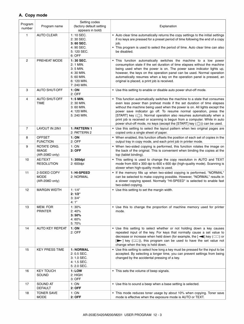
A. Copy mode
Program number
Program nameSetting codes
(factory default setting appears in bold)
Explanation
1 AUTO CLEAR 1: 10 SEC.2: 30 SEC.3: 60 SEC.4: 90 SEC.5: 120 SEC.6: OFF
• Auto clear time automatically returns the copy settings to the initial settingsif no keys are pressed for a preset period of time following the end of a copyjob.
• This program is used to select the period of time. Auto clear time can alsobe disabled.
2 PREHEAT MODE 1: 30 SEC.2: 1 MIN.3: 5 MIN.4: 30 MIN.5: 60 MIN.6: 120 MIN.7: 240 MIN.
• This function automatically switches the machine to a low powerconsumption state if the set duration of time elapses without the machinebeing used when the power is on. The power save indicator lights up,however, the keys on the operation panel can be used. Normal operationautomatically resumes when a key on the operation panel is pressed, anoriginal is placed, a print job is received.
3 AUTO SHUT-OFF 1: ON2: OFF
• Use this setting to enable or disable auto power shut-off mode.
4 AUTO SHUT-OFF TIME
1: 5 MIN.2: 30 MIN.3: 60 MIN.4: 120 MIN.5: 240 MIN.
• This function automatically switches the machine to a state that consumeseven less power than preheat mode if the set duration of time elapseswithout the machine being used when the power is on. All lights except thepower save indicator go off. To resume normal operation, press the[START] key ( ). Normal operation also resumes automatically when aprint job is received or scanning is begun from a computer. While in autopower shut-off mode, no keys (except the [START] key ( )) can be used.
7 LAYOUT IN 2IN1 1: PATTERN 12: PATTERN 2
• Use this setting to select the layout pattern when two original pages arecopied onto a single sheet of paper.
8 OFFSET FUNCTION
1: ON2: OFF
• When enabled, this function offsets the position of each set of copies in theoutput tray in copy mode, and each print job in printer mode.
9 ROTATE ORIG. IMAGE (AR-208D only)
1: ON2: OFF
• When two-sided copying is performed, this function rotates the image onthe back of the original. This is convenient when binding the copies at thetop (tablet binding).
10 AE/TEXT RESOLUTION
1: 300dpi2: 600dpi
• This setting is used to change the copy resolution in AUTO and TEXTmode from 600 x 300 dpi to 600 x 600 dpi (high-quality mode). Scanning isslower when high-quality mode is used.
11 2-SIDED COPY MODE (AR-208D only)
1: HI-SPEED2: NORMAL
• If the memory fills up when two-sided copying is performed, "NORMAL"can be selected to make copying possible. However, "NORMAL" results ina slower copying speed. Normally "HI-SPEED" is selected to enable fasttwo-sided copying.
12 MARGIN WIDTH 1: 1/4"2: 1/2"3: 3/4"4: 1"
• Use this setting to set the margin width.
13 MEM. FOR PRINTER
1: 30%2: 40%3: 50%4: 60%5: 70%
• Use this to change the proportion of machine memory used for printermode.
14 AUTO KEY REPEAT 1: ON2: OFF
• Use this setting to select whether or not holding down a key causesrepeated input of the key. For keys that normally cause a set value todecrease or increase when held down (for example, the [ ] key ( ) or[ ] key ( )), this program can be used to have the set value notchange when the key is held down.
15 KEY PRESS TIME 1: NORMAL2: 0.5 SEC.3: 1.0 SEC.4: 1.5 SEC.5: 2.0 SEC.
• Use this setting to select how long a key must be pressed for the input to beaccepted. By selecting a longer time, you can prevent settings from beingchanged by the accidental pressing of a key.
16 KEY TOUCH SOUND
1: LOW2: HIGH3: OFF
• This sets the volume of beep signals.
17 SOUND AT DEFAULT
1: ON2: OFF
• Use this to sound a beep when a base setting is selected.
18 TONER SAVE MODE
1: ON2: OFF
• This mode reduces toner usage by about 10% when copying. Toner savemode is effective when the exposure mode is AUTO or TEXT.
AR-203E/5420/M200/M201 USER PROGRAM 12 - 3

B. Print mode
*1: The scanning speed increases when the USB 2.0 mode is set to "HI-SPEED", however, the printing speed does not increase considerably.
*2: When the 250-sheet paper feed unit is installed.
19 AE LEVEL ADJUST 1: SPF/RSPF (Adjustment to 5 levels is possible.)
2: DOCUMENT GLASS (Adjustment to 5 levels is possible.)
• This is used to adjust the exposure level.• The automatic exposure level can be adjusted separately for the document
glass and the RSPF.• For the procedure for adjusting the exposure and guidelines for numeric
values. The factory default setting for the exposure level is center.
20 LANGUAGE 1: AMERICAN ENGLISH2: ENGLISH3: FRENCH4: SPANISH
::
• This is used to set the language used in the display.
21 RESET FACTORY 1: Yes2: No
• This is used to return all settings to the factory default settings.
22 SORT AUTO SELECT
1: ON2: OFF
• Use this setting to enable or disable sort auto select mode.
24 CHECK RSPF OPEN
1: ON2: OFF
• You can set the operation that takes place if the [START] key ( ) ispressed when the RSPF is not completely closed. (Valid only when themulti-bypass paper feed is used.)
25 VALID COPY WIDTH
1: 8.5x112: 5.5x8.5
• Set the allowed paper sizes for copying from the bypass tray. When"5.5x8.5" is selected, a copy of a letter size original will only be printed upto invoice size.
28 LSU SETTING 1: ON2: OFF
• Select whether copying is only allowed when the polygon motor is rotating,or also when the polygon motor is stopped.
29 PAPER TYPE 1: PLAIN PAPER2: HEAVY PAPER
• Set the temperature of the fusing unit when the bypass tray is used.Normally "HEAVY PAPER" should be selected.
30 DISPLAY CONTRAST
1: LIGHTER2: LIGHT3: NORMAL4: DARK5: DARKER
• Set the contrast of the display.
Program number
Program nameSetting codes
(factory default setting appears in bold)
Explanation
Program number
Program nameSetting codes
(factory default setting appears in bold)
Explanation
1 FORCED OUTPUT 1: ON2: OFF
• When this function is enabled, printing in printer mode will automaticallycontinue using a different size of paper if the specified size of paper runs outin all trays. This feature does not function in copy mode.
2 USB 2.0 MODE SWITCH *1
1: FULL-SPEED2: HI-SPEED
• This sets the USB 2.0 data transfer speed. To obtain the fastest speed whenusing the USB 2.0 connector, first verify that your computer meets thesystem requirements (operating system and driver), and then use thisprogram to change the USB 2.0 mode to "Hi-Speed". Note that the settingshould not be changed while running a TWAIN driver.
3 AUTO TRAY SWITCH*2
1: ON2: OFF
• If the paper runs out during printing and there is paper of the same size inanother tray, this function automatically switches to that tray (excluding thebypass tray). The function can be disabled.
AR-203E/5420/M200/M201 USER PROGRAM 12 - 4
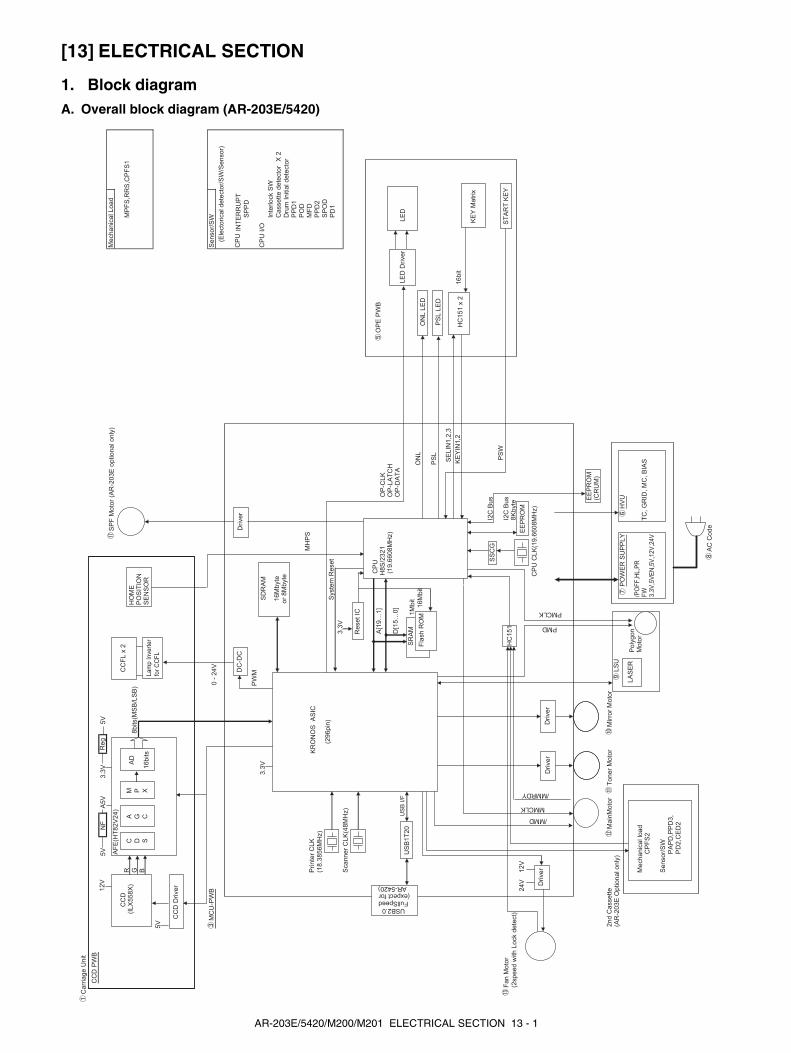
[13] ELECTRICAL SECTION
1. Block diagramA. Overall block diagram (AR-203E/5420)
Carr
iage
Unit
CC
DP
WB
12V
5V
NF
A5V
3.3
VR
eg
5V
SP
FM
oto
r(A
R-2
03E
optionalonly
)M
echanic
alLoad
RM
PF
S,R
RS
,CP
FS
1G
8bits(M
SB
/LS
B)
B
5V
MC
U-P
WB
Sensor/
SW
(Ele
cto
ricaldete
cto
r/S
W/S
ensor)
CP
UIN
TE
RR
UP
T
SP
PD
3.3
VC
PU
I/O
Inte
rlock
SW
Cassett
edete
cto
rX
2
Dru
mIn
itia
ldete
cto
rP
PD
1P
OD
Printe
rC
LK
MF
D
(18.3
856M
Hz)
PP
D2
SP
OD
PD
13.3
VS
canner
CLK
(48M
Hz)
A[1
9…
1]
OP
EP
WB
D[1
5…
0]
US
BI/F
1M
bit
16M
bit
16bit
I2C
Bus
Fan
Moto
rI2
CB
us
(2speed
with
Lock
dete
ct)
8K
byte
24V
12V
2nd
Cassette
Main
Moto
rT
oner
Moto
rM
irro
rM
oto
r(A
R-2
03E
Optionalonly
)
Poly
gon
Mechanic
allo
ad
Moto
r
CP
FS
2
Sensor/
SW
PA
PD
,PP
D3,
PD
2,C
ED
2
AC
Code
LS
U
KR
ON
OS
AS
IC
(296pin
)
CP
UH
8S
/2321
(19.6
608M
Hz) E
EP
RO
M
SD
RA
M
16M
byte
or
8M
byte
ResetIC
SR
AM
Driver
Fla
sh
RO
M
AF
E(H
T82V
24)
C D S
A G C
M P X
AD
16bits
CC
DD
river
CC
FL
x2
Lam
pIn
vert
er
for
CC
FL
HO
ME
PO
SIT
ION
SE
NS
OR
CC
D(I
LX
558X
)
CP
UC
LK
(19.6
608M
Hz)
Syste
mR
eset SS
CG
PMD
Driver
LE
DD
river
LE
D
HC
151
x2
KE
YM
atr
ix
ST
AR
TK
EY
PO
WE
RS
UP
PLY
/PO
FF
,HL,P
RF
W3.3
V,5
VE
N,5
V,1
2V
,24V
HV
U
TC
,G
RID
,M
C,B
IAS
PMCLK
PS
W
KE
YIN
1,2
SE
LIN
1,2
,3
OP
-CLK
OP
-LA
TC
HO
P-D
AT
A
PS
L
MH
PS
Driver
/MMD
PW
M
0-
24V
HC
151
DC
-DC
/MMRDY
EE
PR
OM
(CR
UM
)
LA
SE
R
MMCLK
US
B1T
20
PS
LLE
D
ON
LLE
DO
NL
Driver
USB2.0FullSpeed(expectforAR-5420)
AR-203E/5420/M200/M201 ELECTRICAL SECTION 13 - 1

B. Overall block diagram (AR-M200/M201)
Car
riag
e U
nit
12V
12V
Reg
A5V
3.3V
RS
PF
Mot
or (
AR
-M20
0/M
201
optio
nal o
nly)
R G8b
its (
MS
B/L
SB
)B
AR
-FX
13 (
Opt
ion)
5V
Spe
aker
Mec
hani
cal L
oad
MC
U-P
WB
MP
FS
,RR
S,C
PF
S1
(RS
PF
UN
IT)
SP
US
,SR
VC
3.3V
8Mb
256M
bx2
or 1
6Mb
D[7
..0]
AR
-NB
2A(O
ptio
n)R
D12
MH
zC
SIN
TS
enso
r/S
WP
rinte
r C
LKE
ther
net
(Ele
ctor
ical
det
ecto
r/S
W/S
enso
r)/E
SP
RD
CP
UIN
TE
RR
UP
TS
PP
D18
.385
6MH
z3.
3V18
.385
6MH
zU
AR
TC
PU
I/O
NW
PW
BIn
terlo
ck S
WC
asse
tte d
etec
tor
X 2
Dru
m In
itial
det
ecto
rS
cann
er C
LK (1
2MH
zx4
48M
Hz)
A[1
9…1]
PP
D1
PO
DD
[15…
0]M
FD
PP
D2
1Mbi
tO
PE
PW
BS
PID
SR
JDS
CO
D
Dup
lex
Mod
el O
nly
CP
UC
LK8b
itD
uple
x M
otor
FA
X M
odel
Onl
y
I2C
Bus
8bit
FA
X O
PE
PW
BA
R-F
X13
D[1
5…8]
8Kby
teS
hifte
r M
otor
Buz
zer
Fan
Mot
or24
V12
V
2nd
Cas
sett
eM
ain
Mot
orT
oner
Mot
orM
irror
Mot
or
Mec
hani
cal l
oad
CP
FS
2
Sen
sor/
SW
Pol
ygon
Mot
orP
PD
3,P
D2,
CE
D2
AC
Cod
e
LSU
KR
ON
OS
AS
IC (
296p
in)
CP
UH
8S/2
321
(19.
6608
MH
z)
EE
PR
OM
SD
RA
M8M
byte
Res
et IC
SR
AM
Driv
er
Fla
sh R
OM
AF
E(H
T86
V26
)
C D S
A G C
M P X
AD
16bi
ts
CC
D D
river
CC
FL
x 2
Lam
p In
vert
erfo
r C
CF
L
HO
ME
PO
SIT
ION
SE
NS
OR
CC
D(I
LX55
8K)
CP
U C
LK (
19.6
608M
Hz)
Sys
tem
Res
et SS
CG
PMD
LED
Driv
erLE
D
HC
151
KE
Y M
atrix
ST
AR
T K
EY
PO
WE
R S
UP
PL
Y
/PO
FF,H
L,P
RFW 3.
3V,5
VE
N,5
V,1
2V,2
4V
HV
U
TC
, GR
ID, M
C, B
IAS
PMCLK
PS
W
KE
YIN
SE
LIN
1,2,
3
OP
-CLK
OP
-LA
TC
HO
P-D
AT
A
PS
L
MH
PS
Driv
er
Driv
er
/MMD
PW
M
0 -
24V
DC
-DC
Imag
e B
US
(PI-
Bus
)Im
age
BU
S(P
O-B
us)
OA
982
SD
RA
MF
lash
RO
M
/MMLD
8
KE
YS
CA
N1
- 3
ISP
1583
USB2.0High-speed
P-B
us
LCD
(2 x
20)
FA
X I/
F
HC
238
(3 to
8 d
ecod
e)
EE
PR
OM
(CR
UM
)
LCD
ELC
D R
SLC
D R
/W (
TB
D)
LCD
DB
7-4
FA
X M
ain
PC
BA
Driv
er
IO A
SIC
LAS
ER
KE
Y M
atrix
LED
MMCLK
PS
L LE
D
8
SS
CG
PMRDY
Driv
er
Net
wor
k B
ox10
0Bas
e-T
Driv
er
16M
bit
AR-203E/5420/M200/M201 ELECTRICAL SECTION 13 - 2
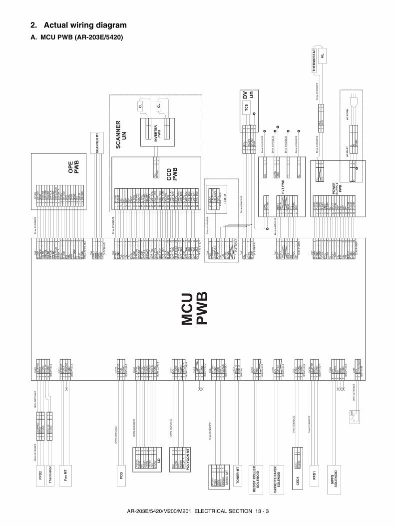
2. Actual wiring diagramA. MCU PWB (AR-203E/5420)
DH
AI-
0519Q
SP
ZD
HA
I-0287Q
SZ
ZC
N22
CN
2D
HA
I-0513Q
SP
ZC
N304
1LE
DP
PD
21
LE
DP
PD
21
12
PP
D2
22
23
D-G
ND
33
34
41
RT
H_IN
15
52
D-G
ND
2B
5B
-PH
-K-S
66
77
88
CN
11
99
10
10
11
11
12
12
13
13
B4B
-PH
-K-S
14
14
15
15
16
16
17
17
18
18
IMS
A-9
619S
-18A
CN
41 2 3 4
B4B
-PH
-K-R
CN
3D
HA
I-0268Q
SZ
4D
HA
I-0286Q
SZ
ZC
N19
11
22
33
44
B3B
-PH
-K-S
55
66
77
DH
AI-
0530Q
SP
ZC
N42
88
-H
SY
NC
89
9D
-GN
D7
10
10
+5V
611
11
512
12
-LD
EN
413
13
-V
IDE
O3
14
14
-S
/H2
15
15
D-G
ND
116
16
1B
08B
-CZ
HK
-B17
17
218
18
19
19
20
20
21
21
DH
AI-
0529Q
SP
ZC
N41
22
22
523
23
424
24
325
25
226
26
127
27
B05B
-CZ
HK
-B28
28
29
29
30
30
CN
25
31
31
32
32
PD
1F
F4-3
2-S
15D
5
B3B
-PH
-K-M
CN
5D
HA
I-0516Q
SP
ZD
HA
I-0514Q
SP
ZC
N6
22
14
42
63
38
1
MM
LD
4M
MLD
1P
18-F
X-4
S-C
/MM
CLK
5/M
MC
LK
3B
5B
-PA
SK
-15 7 9
CN
23
10
TM
A_O
B10B
-PH
DS
S-B
TM
B_O
B2P
-VH
CN
5D
HA
I-0526Q
SP
Z1
11
22
23
66
CN
12
45
5B
4B
-PH
-K-R
88
/RR
S
B3B
-PH
-K-E
DH
AI-
0515Q
SP
Z1
12
CN
10
DH
AI-
0273Q
SZ
ZC
N1
DH
AI-
0525Q
SP
Z1
11
42
2B
3B
-PH
-K-S
33
44
DH
AI-
0292Q
SZ
Z5
51
66
DH
AI-
0269Q
SZ
ZC
N7
77
CE
D1
18
8D
HA
I-0267Q
SP
ZD
-GN
D2
B24B
-PN
DZ
S-1
1
B3B
-PH
-K-K
DH
AI-
0289Q
SZ
ZC
N16
CN
19
110
21
DH
AI-
0536Q
SP
ZD
HA
I-0537Q
SP
ZB
3B
-PH
-K-R
11
32
11
12
4H
LN
22
13
514
6C
N26
15
71
16
82
17
93
18
10
419
11
520
12
B5B
-PH
-K-R
21
13
22
14
23
15
L1
L
DH
AI-
0272Q
SZ
ZC
N15
24
16
N2
N
B24B
-PN
DZ
S-1
B2P
-VH
-R
(CR
UM
SD
A)
(CR
UM
SC
L)
PG
ND
5V
EN
PG
ND
(CR
UM
SD
A)
(CR
UM
SC
L)
24V
P-G
ND
D-G
ND
TC
SD
VS
EL
24V
5V
EN
/PM
DP
MR
DY
PM
CLK
_A
INT
24V
/MM
DP
GN
D
(AF
E_D
B4)
(AF
E_D
B3)
/CP
FS
1
1
INT
24V
PG
ND
/MM
D
12 3
HLN
HLL
HLL
3
GR
IDM
CF
B
TC
/MC
/BIA
S/T
C
24V
1
SH
OLD
/SY
NC
INT
5V
D-G
ND
/LD
EN
/VID
EO
8 1 21 2D
-GN
D
23 4 5 1
12V
IN24V
FW
P-G
ND
24V
/PR
HLO
UT
P-G
ND
EN
5V
3.3
VIN
5V
/PO
FF
D-G
ND
P-G
ND
D-G
ND
3.3
VIN
/PR
HLO
UT
P-G
ND
P-G
ND
12V
IN24V
FW
24V
EN
5V
3.3
VIN
5V
/PO
FF
D-G
ND
P-G
ND
D-G
ND
3.3
VIN
BC
/BIA
S/T
C/G
RID
L/M
C
BIA
SF
-GN
DM
C
/GR
IDL
INT
5V
INT
24V
INT
5V
INT
24V
BIA
S
24V
TC
SD
VS
EL
D-G
ND
24V
DV
SE
LT
CS
(AF
E_D
B0)
(AF
E_D
B4)
(AF
E_D
B3)
(AF
E_D
B2)
(AF
E_D
B1)
D-G
ND
(AD
CLK
)D
-GN
D(A
FE
_S
CK
)(A
FE
_D
B7)
MH
PS
(AF
E_D
B6)
CC
D_P
HI1
(AF
E_S
EN
)
(AF
E_D
B5)
VC
LP
-GN
D
CC
D-C
P(A
FE
_S
DI)
CC
D_P
HI2
D-G
ND
CC
D-T
GD
-GN
DC
CD
-RS
(BS
AM
P)
2
P-G
ND
P-G
ND
VC
LV
CL
12V
12V
EN
5V
D-G
ND
(VS
AM
P)
1 1321 2 1 253 46 721 2 3 4 2
D-G
ND
D-G
ND
P-G
ND
24V
(AF
E_S
EN
)
(AD
CLK
)D
-GN
D
VC
LV
CL
12V
12V
D-G
ND
53 44 1 2 35
SE
LIN
2
KE
YIN
2#
PS
W
D-G
ND
PS
L
ON
L
OP
-DA
TA
EN
5V
3
D-G
ND
PM
CLK
_A
3
D-G
ND
LE
DP
OD
PO
D
SE
LIN
3
OU
TB
+O
UT
A-
OU
TB
-
OU
TA
+
D-G
ND
DR
ST
SE
LIN
1O
P-C
LK
D-G
ND
D-G
ND
KIN
1K
EY
IN1#
SE
LIN
3S
TR
OB
E
VF
MO
UT
PP
D2
D-G
ND
D-G
ND
RT
H_IN
FA
NLK
/VF
MC
NT
PG
ND
24V
PM
RD
Y/P
MD
D-G
ND
OP
-ST
B
D-G
ND
(VS
AM
P)
CC
D-T
G
P-G
ND
P-G
ND
OP
-LA
TC
H
PS
LO
NL
PS
W
EN
5V
(AF
E_D
B0)
(AF
E_D
B2)
(AF
E_D
B1)
(AF
E_D
B7)
(AF
E_D
B5)
(AF
E_D
B6)
mt_
at_
hom
e
D-G
ND
(AF
E_S
CK
)
3
PP
D1
D-G
ND
CE
D1
D-G
ND
LE
DP
PD
1
1 2D
-GN
D3
24V
1(D
SW
S)
5 MF
DD
GN
D
/MP
FS
24V
CC
D-R
S(B
SA
MP
)C
CD
-CP
(AF
E_S
DI)
CC
D_P
HI2
D-G
ND
CC
D_P
HI1
D-G
ND
OP
-DA
TA
5V
EN
SE
LIN
1O
P-C
LK
SE
LIN
2
OP
-LA
TC
H
PG
ND
KIN
2
5V
DR
ST
D-G
ND
5V
24V
PPD
2
Thermistor
FanMT
POD
POLYGONMT
LD
TONERMT
RESISTROLLER
SOLENOID
CASSETTEPAPER
SOLENOID
CED
1 PPD
1
DS
W
OPE
PWB
SCANNERMT
CCD
PWB
INVERTER
PWB
CL
CL
TCSDVun
HVTPWB
POWER
SUPPLY
PWB
MCU
PWB
MA
INM
T
THERMOSTAT
SCANNER
UN
MPFS
SOLENOID
HL
CR
UM
AC-INLET
AC-CORD
AR-203E/5420/M200/M201 ELECTRICAL SECTION 13 - 3
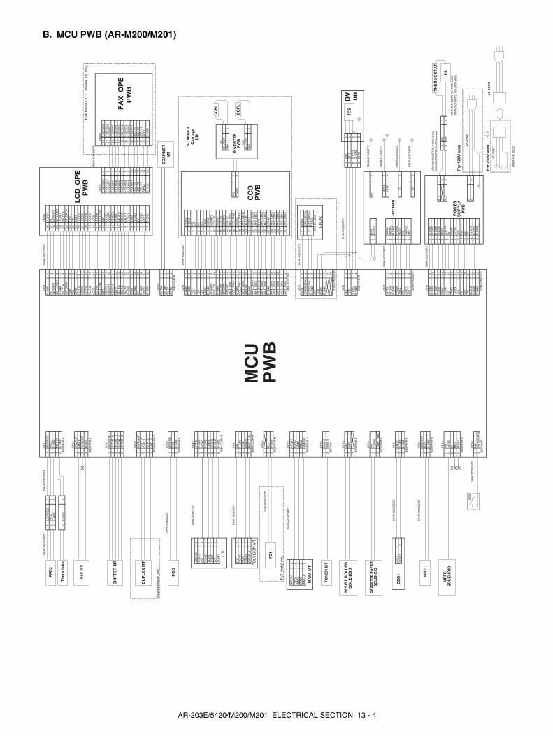
B. MCU PWB (AR-M200/M201)D
HA
I-05
19Q
SP
ZD
HA
I-02
87Q
SZ
ZC
N11
CN
3D
HA
I-05
17Q
SP
ZC
N30
21
LED
PP
D2
1LE
DP
PD
21
322
PP
D2
22
313
D-G
ND
33
304
295
282
D-G
ND
2B
5B-P
H-K
-S6
277
268
25C
N16
924
1023
1122
1221
1320
FA
XM
odel
/FX
13O
ptio
nalK
ITon
lyB
4B-P
H-K
-S14
1915
18D
HA
I-05
43Q
SP
Z16
1717
16C
N30
1C
N40
118
151
15C
N27
1914
214
2013
313
2112
412
2211
511
2310
610
249
79
258
88
267
97
276
106
285
115
CN
2029
412
430
313
331
214
232
115
1
B05
B-X
AS
K-1
Dup
lex
Mod
elon
lyC
N22
1
DH
AI-
0286
QS
ZZ
CN
262 3 4
B4B
-PH
-K-R
B3B
-PH
-K-S
CN
4D
HA
I-02
68Q
SZ
41
1
DH
AI-
0530
QS
P1
CN
422
2
-HS
YN
C8
33
D-G
ND
74
4
+5V
65
5
56
6
-LD
EN
47
7
-VID
EO
38
8
-S/H
29
9
D-G
ND
110
10
B08
B-C
ZH
K-B
1111
1212
CN
213
1314
1415
15D
HA
I-05
29Q
SP
1C
N41
1616
15
1717
24
1818
319
19C
N3
220
201
2121
B05
B-C
ZH
K-B
2222
2323
2424
CN
2825
25D
HA
I-04
23Q
SZ
Z26
26P
D1
2727
2828
B3B
-PH
-K-M
2929
3030
FA
XM
odel
only
3131
3232
DH
AI-
0514
QS
PZ
CN
12FF
4-32
-S15
D5
1 2 3M
MLD
4M
MLD
CN
7D
HA
I-05
16Q
SP
Z
/MM
CLK
5/M
MC
LK2
2
B5B
-PA
SK
-14
46
38
11
P18
-FX
-4S
-C3
CN
255
TM
A_O
7T
MB
_O9
B2P
-VH
10B
10B
-PH
DS
S-B
CN
18C
N6
DH
AI-
0526
QS
PZ
11
1/R
RS
22
23
66
B3B
-PH
-K-E
45
5B
4B-P
H-K
-R8
8
CN
15D
HA
I-05
15Q
SP
Z1
MC
12
B3B
-PH
-K-S
DH
AI-
0273
QS
ZZ
CN
2D
HA
I-05
25Q
SP
Z1
11
42
2D
HA
I-02
69Q
SZ
ZC
N21
33
CE
D1
14
4D
HA
I-02
92Q
SZ
ZD
-GN
D2
55
16
6B
3B-P
H-K
-K7
78
8D
HA
I-02
67Q
SP
ZB
24B
-PN
DZ
S-1
1
DH
AI-
0289
QS
ZZ
CN
24
CN
2D
HA
I-05
25Q
SP
Z
B3B
-PH
-K-R
91
102
DH
AI-
0510
QS
P1
(for
100V
area
)11
3D
HA
I-05
36Q
SP
Z(f
or20
0Var
ea)
124
HLL
1C
N14
135
21
11
146
HLN
22
215
73
168
DH
AI-
0511
QS
P1
(for
100V
area
)4
179
DH
AI-
0537
QS
PZ
(for
200V
area
)5
1810
Fo
r12
0Var
eaB
5B-P
H-K
-R19
1120
1221
13L
1D
HA
I-02
72Q
SZ
ZC
N10
2214
N2
2315
2416
B2P
-VH
-RB
24B
-PN
DZ
S-1
Fo
r20
0Var
ea
DH
AI-
0491
QS
ZZ
MC
FB
GR
ID
TC
BC
LED
_V2
LED
_V1
DA
TA
1D
-GN
D
F-K
EY
IN3
F-K
EY
IN2
F-K
EY
IN1
LED
_V3
LED
_V1
DA
TA
1D
-GN
D
F-K
EY
SC
3F
-KE
YS
C2
F-K
EY
SC
1F-
KE
YIN
7F-
KE
YIN
6F-
KE
YIN
5F-
KE
YIN
4
F-K
EY
IN1
LED
_V3
LED
_V2
F-K
EY
SC
3F
-KE
YS
C2
F-K
EY
SC
1
F-K
EY
IN4
F-K
EY
IN3
F-K
EY
IN2
F-K
EY
IN7
F-K
EY
IN6
F-K
EY
IN5
124
VD
upM
T
(AF
E_D
B6)
D-G
ND
(AF
E_D
B4)
(AF
E_D
B3)
(AF
E_S
CK
)
mt_
at_h
ome
(AF
E_D
B5)
AC
VO
UT
D-G
ND
DV
SE
L
24V
TC
S
5VE
N(C
RU
MS
DA
)
(AF
E_D
B2)
1D
-GN
DG
ND
3
CC
D_P
HI1
(AF
E_S
EN
)(A
FE
_SE
N)
(AD
CLK
)(A
DC
LK)
CC
D_P
HI1
CC
D_P
HI2
VC
LD
-GN
DP
-GN
D
CC
D-C
PG
ND
3(A
FE
_SD
I)
(BS
AM
P)
(BS
AM
P)
AC
VO
UT
1
D-G
ND
D-G
ND
CC
D-R
SC
CD
-RS
(VS
AM
P)
(VS
AM
P)
CC
D-T
GC
CD
-TG
EN
5VE
N5V
D-G
ND
D-G
ND
12V
12V
12V
12V
VC
LV
CL
VC
LV
CL
OU
TB
-
P-G
ND
P-G
ND
P-G
ND
P-G
ND
/SF
TM
T_3
OU
TA
+O
UT
B+
OU
TA
-
5V D-G
ND
VC
C3
D-G
ND
/SF
TM
T_0
3/S
FT
MT
_14
/SF
TM
T_2
LCD
E
3/D
MT
_1
LCD
RS
LCD
CO
NT
BZ
R
LCD
RS
/DM
T_0
124
VS
FT
MT
24V
/MP
FS
24V
24V
1(D
SW
S)
5 MF
DD
GN
D
3
PP
D1
D-G
ND
CE
D1
D-G
ND
LED
PP
D1
1 2D
-GN
D3
(AF
E_D
B1)
(AF
E_D
B0)
(AF
E_D
B7)
FA
NLK
/VF
MC
NT
PG
ND
CC
D-C
P(A
FE
_SD
I)C
CD
_PH
I2D
-GN
D
OP
_LA
TC
H
PS
W
LCD
D6
LCD
D5
PS
LD
RS
T
D-G
ND
24V
/DM
T_3
/DM
T_2
PM
RD
Y/P
MD
D-G
ND
D-G
ND
BL
INF
OLE
DO
P_L
AT
CH
VF
MO
UT
PP
D2
D-G
ND
D-G
ND
RT
H_I
N
D-G
ND
BL
INF
OLE
D
BZ
RLC
DC
ON
T
D-G
ND
OP
_CLK
LCD
D7
LCD
D4
OP
_CLK
OP
_DA
TA
PS
W
D-G
ND
PM
CLK
_A
3
D-G
ND
LED
PO
DP
OD
5
OP
_DA
TA
LCD
ELC
DD
4
LCD
D7
LCD
D6
LCD
D5
PS
LD
RS
T
3 4 1 2 34 522 5
D-G
ND
53 4 8 1 2
D-G
ND
P-G
ND
24V
1 253 4 1 2 1 132 2
D-G
ND
(AF
E_S
CK
)(A
FE
_DB
7)M
HP
S(A
FE
_DB
5)(A
FE
_DB
6)D
-GN
D(A
FE
_DB
4)(A
FE
_DB
3)(A
FE
_DB
2)
5VE
N(C
RU
MS
DA
)
(AF
E_D
B1)
(AF
E_D
B0)
(CR
UM
SC
L)P
-GN
D
D-G
ND
D-G
ND
24V
DV
SE
LT
CS
(CR
UM
SC
L)D
-GN
D
BIA
S
24V
TC
SD
VS
EL
BIA
SF
-GN
D
/GR
IDL
INT
5VIN
T24
V
P-G
ND
INT
5VIN
T24
VP
-GN
D
/BIA
S
/GR
IDL
/MC
D-G
ND
/MC
5V /PO
FF
12V
IN
P-G
ND
D-G
ND
3.3V
INE
N5V
24V
FW
24V
/PR
HLO
UT
P-G
ND
P-G
ND
D-G
ND
P-G
ND
D-G
ND
3.3V
INE
N5V
3.3V
IN5V
1
P-G
ND
24V
/PR
HLO
UT
P-G
ND
/PO
FF
12V
IN24
VF
W
1
SH
OLD
/SY
NC
INT
5VD
-GN
D
/LD
EN
/VID
EO
6 72
/PM
DP
MR
DY
PM
CLK
_A
2 3
INT
24V
/MM
DP
GN
D
24V
/CP
FS
1
1
INT
24V
PG
ND
/MM
D
223 4 5
HLN
HLL
3
P-G
ND
/BIA
S/T
C
P-G
ND
3.3V
IN
/TC
1
24V
P-G
ND
KE
YIN
SE
LIN
3S
ELI
N2
SE
LIN
1D
-GN
DE
N5V
D-G
ND
KE
YS
C1
KE
YS
C2
KE
YS
C3
1 21 2 3 4
KE
YS
C1
KE
YS
C2
KE
YS
C3
KE
YIN
SE
LIN
3S
ELI
N2
SE
LIN
1D
-GN
D
VC
C3
D-G
ND
EN
5VD
-GN
D5V D
-GN
D
PP
D2
Th
erm
isto
r
Fan
MT
PO
D
PO
LYG
ON
MT
LD
TO
NE
RM
T
RE
SIS
TR
OL
LE
RS
OL
EN
OID
CA
SS
ETT
EP
AP
ER
SO
LEN
OID
CE
D1 PP
D1
DS
W
LC
D_O
PE
PW
B
TC
SD
V un
HV
TP
WB
PO
WE
RS
UP
PL
YP
WB
AC
-CO
RD
MC
UP
WB
MA
INM
T
DU
PL
EX
MT
TH
ER
MO
ST
AT
HL
MP
FS
SO
LE
NO
ID
SH
IFT
ER
MT
SC
AN
NE
RM
T
CC
DP
WB
INV
ER
TE
RP
WB
CC
FL
CC
FL
SC
AN
NE
RC
arri
age
UN
CR
UM
PD
1
FA
X_O
PE
PW
B
AC
-IN
LET
AC
-CO
RD
AR-203E/5420/M200/M201 ELECTRICAL SECTION 13 - 4

C. SPF unit (AR-203E optional only)
D. RSPF unit (AR-M200/M201 optional only)
E. 2nd cassette unit (AR-203E/M200/M201 optional only)
CN24 DHAI-0532QSP1
B12B-PH-K-S
A
6 /A
5 COMA
2 COMB
4
SPID
2 DGND
3 B
1 /B
1
3 LEDSPID
1 SPPD
2 DGND
3 LEDSPPD
DGND 11
LEDSPPD 12
LEDSPID 9
SPPD 10
SPID 7
DGND 8
SPMT_1 5
SPMT_3 6
SPMT_0 3
SPMT_2 4
24VSPFMT 1
24VSPFMT 2
MCUPWB
SPID
SPMT
SPF UNIT
SPPD
CN30 DHAI-0533QSPZ DHAI-0541QSPZ
DHAI-0540QSPZ
DHAI-0539QSPZ
B24B-PNDZS-1
/BCOMBBA
/A
24V 12 SRVC 2
2 _SPUS 21
1 SPID 11 24V 1
3 LED_SPID 32 D-GND 2
1
21 SPPD 1
3 LED_SRJD 32 D-GND 21 SRJD
SPID2 DGND3 LEDSPID
1 SCOD2 DGND
3 LED_SPPD 32 D-GND
2 DGND3 LEDSPPD
3 LEDSRJD
1 SPPD
LEDSCOD
SRJD2 DGND1
6
3
1
3
1
5 COMA
2
4
LED_SRJD 1
LED_SPPD 2
DGND 3
DGND 4
SRJD 5
SPPD 6LED_SCOD 7
LED_SPID 8
DGND 9
DGND 10
SCOD 11
SPID 12
NC 15
SPMT_1 16
24VSPFSOL 13
24VSPFSOL 17
SPMT_2 18
SPMT_3 14
SPUS 19
SPMT_0 20
24VSPFSOL 21
24VSPFMT 22
SRVC 23
24VSPFMT 24
MCUPWB
SRJD
SPMT
RSPF UNIT
SPPD
SCOD
SPID
SPUS
SRVC
AR-203E: CN18AR-M200/AR-M201: CN19
B14B-PHDSS-B
DHAI-0442QSZZ DHAI-0441QSZZ
14 /CPFS2 113 24V 211 5V 48 PPD3 77 D-GND 86 PD2 94 D-GND 112 CED2 131 D-GND 149 FG 612 310 5
1 24V 1
3 12
CED2 1D-GND 2
5 10
3PPD3 2
PD2 1
D-GND 1
5V
D-GND 2
D-GND
/CPFS224V5VPPD3D-GNDPD2D-GND
3569
247
CED214
10
2 /CPFS2 2
8111213
1
MCU PWB
CPFS2
PPD3
PD2
CED2
2nd CASSETTE UN
AR-203E/5420/M200/M201 ELECTRICAL SECTION 13 - 5

F. Network box and FAX (AR-M200/M201 optional only)
3. Signal name listSignal name Name Function/Operation Section
(ADCLK) AFE AFE control signal Scanner unit section(AFE_DB0) AFE Image scan data Scanner unit section(AFE_DB1) AFE Image scan data Scanner unit section(AFE_DB2) AFE Image scan data Scanner unit section(AFE_DB3) AFE Image scan data Scanner unit section(AFE_DB4) AFE Image scan data Scanner unit section(AFE_DB5) AFE Image scan data Scanner unit section(AFE_DB6) AFE Image scan data Scanner unit section(AFE_DB7) AFE Image scan data Scanner unit section(AFE_SCK) AFE AFE control signal Scanner unit section(AFE_SDI) AFE AFE serial data Scanner unit section(AFE_SEN) AFE AFE control signal Scanner unit section(BSAMP) AFE AFE control signal Scanner unit section(VSAMP) AFE AFE control signal Scanner unit section/BIAS HV bias signal HV bias drive Process section/CPFS1 1st CS pickup solenoid Paper transport section/CPFS2 2nd CS pickup solenoid 2nd cassette section/DMT_0 DUP motor DUP motor phase control Duplex drive section/DMT_1 DUP motor DUP motor phase control Duplex drive section/DMT_2 DUP motor DUP motor phase control Duplex drive section/DMT_3 DUP motor DUP motor phase control Duplex drive section/FAX_RST FAX PWB reset signal FAX optional section/GRIDL HV grid signal Main charger grid control Process section/LDEN Laser Laser circuit control signal LSU/MC HV MC signal Main charger control Process section/MDM_IRQ FAX PWB interrupt FAX optional section/MMCLK Main motor Clock signal to the polygon motor Main drive section/MMD Main motor Polygon motor drive signal Main drive section/MPFS Multi bypass solenoid Paper transport section/PMD Polygon motor Polygon motor drive signal LSU/POFF Low voltage power Output power control Power section/PR Heater lamp Power relay control Power section
FAX Model / FX13 Optional Model Only
DHAI-0538QSPZCN5 CN2 CN3
B02B-PH-K-S
MJ2
MJ1
CN8 USB Cable CN11 VBUS 12 23 34 4567 CN989
PJ1
DHAI-0544QSPZ CN3
AR-NB2A Optional Model only
VCC
LK_LED12
5V 10
TPTX+TPTX-TPRX+
2GND 3
D-D+
NCST_LED
FG
115V
1 L1 L 1
5TPRX-NC
GNDNCNC
32 2N N
5 FG
3 D+4 GND
1 5V2 D-
1 BT12 LT1
5 LT26 BT2
3 TEL14 TEL2
1 BT12 LT1
5 NC6 NC
3 L14 L2
1 NC2 NC
40 D-GND39 P-GND
38 VCC337 EN5V
36 24V35 MDM_IRQ
34 FAX_RST33 PB_NOE
32 PB_NWE31 PB_NAE0
30 PB_NCS129 PB_ADDR0
28 PB_ADDR127 PB_ADDR2
26 PB_ADDR325 PB_ADDR4
24 PB_DATA523 PB_ADDR6
22 PB_ADDR721 PB_DATA0
20 PB_DATA119 PB_DATA2
18 PB_DATA317 PB_DATA4
16 PB_DATA515 PB_DATA6
14 PB_DATA713 MCU_INT
12 MCU_nCS11 /RD
10 MCU_D09 MCU_D1
8 MCU_D27 MCU_D3
6 MCU_D45 MCU_D5
4 MCU_D63 MCU_D7
2 MODEM_IN1 D-GND
39 D-GND40 P-GND
37 VCC338 EN5V
35 24V36 MDM_IRQ
33 FAX_RST34 PB_NOE
31 PB_NWE32 PB_NAE0
29 PB_NCS130 PB_ADDR0
27 PB_ADDR128 PB_ADDR2
25 PB_ADDR326 PB_ADDR4
23 PB_DATA524 PB_ADDR6
21 PB_ADDR722 PB_DATA0
19 PB_DATA120 PB_DATA2
17 PB_DATA318 PB_DATA4
15 PB_DATA516 PB_DATA6
13 PB_DATA714 MCU_INT
11 MCU_nCS12 /RD
9 MCU_D010 MCU_D1
7 MCU_D28 MCU_D3
5 MCU_D46 MCU_D5
3 MCU_D64 MCU_D7
1 MODEM_IN2 D-GND
MCUPWB
FAXMainPWB
ToTEL
CommunicationLine
ToTEL
CommunicationLine
Speaker
NW BoxPWB
ToLAN
AC adapter
POWERSUPPLY
PWB
AR-203E/5420/M200/M201 ELECTRICAL SECTION 13 - 6
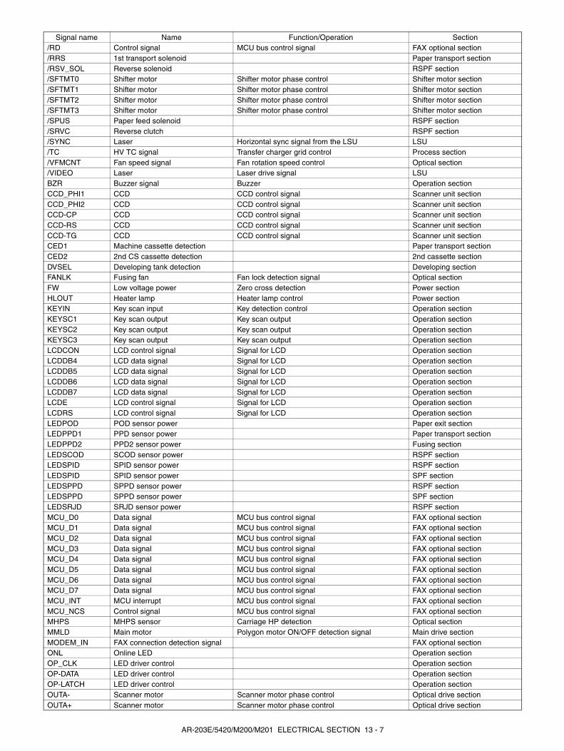
/RD Control signal MCU bus control signal FAX optional section/RRS 1st transport solenoid Paper transport section/RSV_SOL Reverse solenoid RSPF section/SFTMT0 Shifter motor Shifter motor phase control Shifter motor section/SFTMT1 Shifter motor Shifter motor phase control Shifter motor section/SFTMT2 Shifter motor Shifter motor phase control Shifter motor section/SFTMT3 Shifter motor Shifter motor phase control Shifter motor section/SPUS Paper feed solenoid RSPF section/SRVC Reverse clutch RSPF section/SYNC Laser Horizontal sync signal from the LSU LSU/TC HV TC signal Transfer charger grid control Process section/VFMCNT Fan speed signal Fan rotation speed control Optical section/VIDEO Laser Laser drive signal LSUBZR Buzzer signal Buzzer Operation sectionCCD_PHI1 CCD CCD control signal Scanner unit sectionCCD_PHI2 CCD CCD control signal Scanner unit sectionCCD-CP CCD CCD control signal Scanner unit sectionCCD-RS CCD CCD control signal Scanner unit sectionCCD-TG CCD CCD control signal Scanner unit sectionCED1 Machine cassette detection Paper transport sectionCED2 2nd CS cassette detection 2nd cassette sectionDVSEL Developing tank detection Developing sectionFANLK Fusing fan Fan lock detection signal Optical sectionFW Low voltage power Zero cross detection Power sectionHLOUT Heater lamp Heater lamp control Power sectionKEYIN Key scan input Key detection control Operation sectionKEYSC1 Key scan output Key scan output Operation sectionKEYSC2 Key scan output Key scan output Operation sectionKEYSC3 Key scan output Key scan output Operation sectionLCDCON LCD control signal Signal for LCD Operation sectionLCDDB4 LCD data signal Signal for LCD Operation sectionLCDDB5 LCD data signal Signal for LCD Operation sectionLCDDB6 LCD data signal Signal for LCD Operation sectionLCDDB7 LCD data signal Signal for LCD Operation sectionLCDE LCD control signal Signal for LCD Operation sectionLCDRS LCD control signal Signal for LCD Operation sectionLEDPOD POD sensor power Paper exit sectionLEDPPD1 PPD sensor power Paper transport sectionLEDPPD2 PPD2 sensor power Fusing sectionLEDSCOD SCOD sensor power RSPF sectionLEDSPID SPID sensor power RSPF sectionLEDSPID SPID sensor power SPF sectionLEDSPPD SPPD sensor power RSPF sectionLEDSPPD SPPD sensor power SPF sectionLEDSRJD SRJD sensor power RSPF sectionMCU_D0 Data signal MCU bus control signal FAX optional sectionMCU_D1 Data signal MCU bus control signal FAX optional sectionMCU_D2 Data signal MCU bus control signal FAX optional sectionMCU_D3 Data signal MCU bus control signal FAX optional sectionMCU_D4 Data signal MCU bus control signal FAX optional sectionMCU_D5 Data signal MCU bus control signal FAX optional sectionMCU_D6 Data signal MCU bus control signal FAX optional sectionMCU_D7 Data signal MCU bus control signal FAX optional sectionMCU_INT MCU interrupt MCU bus control signal FAX optional sectionMCU_NCS Control signal MCU bus control signal FAX optional sectionMHPS MHPS sensor Carriage HP detection Optical sectionMMLD Main motor Polygon motor ON/OFF detection signal Main drive sectionMODEM_IN FAX connection detection signal FAX optional sectionONL Online LED Operation sectionOP_CLK LED driver control Operation sectionOP-DATA LED driver control Operation sectionOP-LATCH LED driver control Operation sectionOUTA- Scanner motor Scanner motor phase control Optical drive sectionOUTA+ Scanner motor Scanner motor phase control Optical drive section
Signal name Name Function/Operation Section
AR-203E/5420/M200/M201 ELECTRICAL SECTION 13 - 7
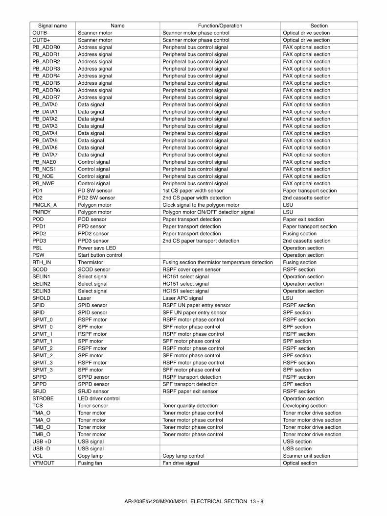
OUTB- Scanner motor Scanner motor phase control Optical drive sectionOUTB+ Scanner motor Scanner motor phase control Optical drive sectionPB_ADDR0 Address signal Peripheral bus control signal FAX optional sectionPB_ADDR1 Address signal Peripheral bus control signal FAX optional sectionPB_ADDR2 Address signal Peripheral bus control signal FAX optional sectionPB_ADDR3 Address signal Peripheral bus control signal FAX optional sectionPB_ADDR4 Address signal Peripheral bus control signal FAX optional sectionPB_ADDR5 Address signal Peripheral bus control signal FAX optional sectionPB_ADDR6 Address signal Peripheral bus control signal FAX optional sectionPB_ADDR7 Address signal Peripheral bus control signal FAX optional sectionPB_DATA0 Data signal Peripheral bus control signal FAX optional sectionPB_DATA1 Data signal Peripheral bus control signal FAX optional sectionPB_DATA2 Data signal Peripheral bus control signal FAX optional sectionPB_DATA3 Data signal Peripheral bus control signal FAX optional sectionPB_DATA4 Data signal Peripheral bus control signal FAX optional sectionPB_DATA5 Data signal Peripheral bus control signal FAX optional sectionPB_DATA6 Data signal Peripheral bus control signal FAX optional sectionPB_DATA7 Data signal Peripheral bus control signal FAX optional sectionPB_NAE0 Control signal Peripheral bus control signal FAX optional sectionPB_NCS1 Control signal Peripheral bus control signal FAX optional sectionPB_NOE Control signal Peripheral bus control signal FAX optional sectionPB_NWE Control signal Peripheral bus control signal FAX optional sectionPD1 PD SW sensor 1st CS paper width sensor Paper transport sectionPD2 PD2 SW sensor 2nd CS paper width detection 2nd cassette sectionPMCLK_A Polygon motor Clock signal to the polygon motor LSUPMRDY Polygon motor Polygon motor ON/OFF detection signal LSUPOD POD sensor Paper transport detection Paper exit sectionPPD1 PPD sensor Paper transport detection Paper transport sectionPPD2 PPD2 sensor Paper transport detection Fusing sectionPPD3 PPD3 sensor 2nd CS paper transport detection 2nd cassette sectionPSL Power save LED Operation sectionPSW Start button control Operation sectionRTH_IN Thermistor Fusing section thermistor temperature detection Fusing sectionSCOD SCOD sensor RSPF cover open sensor RSPF sectionSELIN1 Select signal HC151 select signal Operation sectionSELIN2 Select signal HC151 select signal Operation sectionSELIN3 Select signal HC151 select signal Operation sectionSHOLD Laser Laser APC signal LSUSPID SPID sensor RSPF UN paper entry sensor RSPF sectionSPID SPID sensor SPF UN paper entry sensor SPF sectionSPMT_0 RSPF motor RSPF motor phase control RSPF sectionSPMT_0 SPF motor SPF motor phase control SPF sectionSPMT_1 RSPF motor RSPF motor phase control RSPF sectionSPMT_1 SPF motor SPF motor phase control SPF sectionSPMT_2 RSPF motor RSPF motor phase control RSPF sectionSPMT_2 SPF motor SPF motor phase control SPF sectionSPMT_3 RSPF motor RSPF motor phase control RSPF sectionSPMT_3 SPF motor SPF motor phase control SPF sectionSPPD SPPD sensor RSPF transport detection RSPF sectionSPPD SPPD sensor SPF transport detection SPF sectionSRJD SRJD sensor RSPF paper exit sensor RSPF sectionSTROBE LED driver control Operation sectionTCS Toner sensor Toner quantity detection Developing sectionTMA_O Toner motor Toner motor phase control Toner motor drive sectionTMA_O Toner motor Toner motor phase control Toner motor drive sectionTMB_O Toner motor Toner motor phase control Toner motor drive sectionTMB_O Toner motor Toner motor phase control Toner motor drive sectionUSB +D USB signal USB sectionUSB -D USB signal USB sectionVCL Copy lamp Copy lamp control Scanner unit sectionVFMOUT Fusing fan Fan drive signal Optical section
Signal name Name Function/Operation Section
AR-203E/5420/M200/M201 ELECTRICAL SECTION 13 - 8
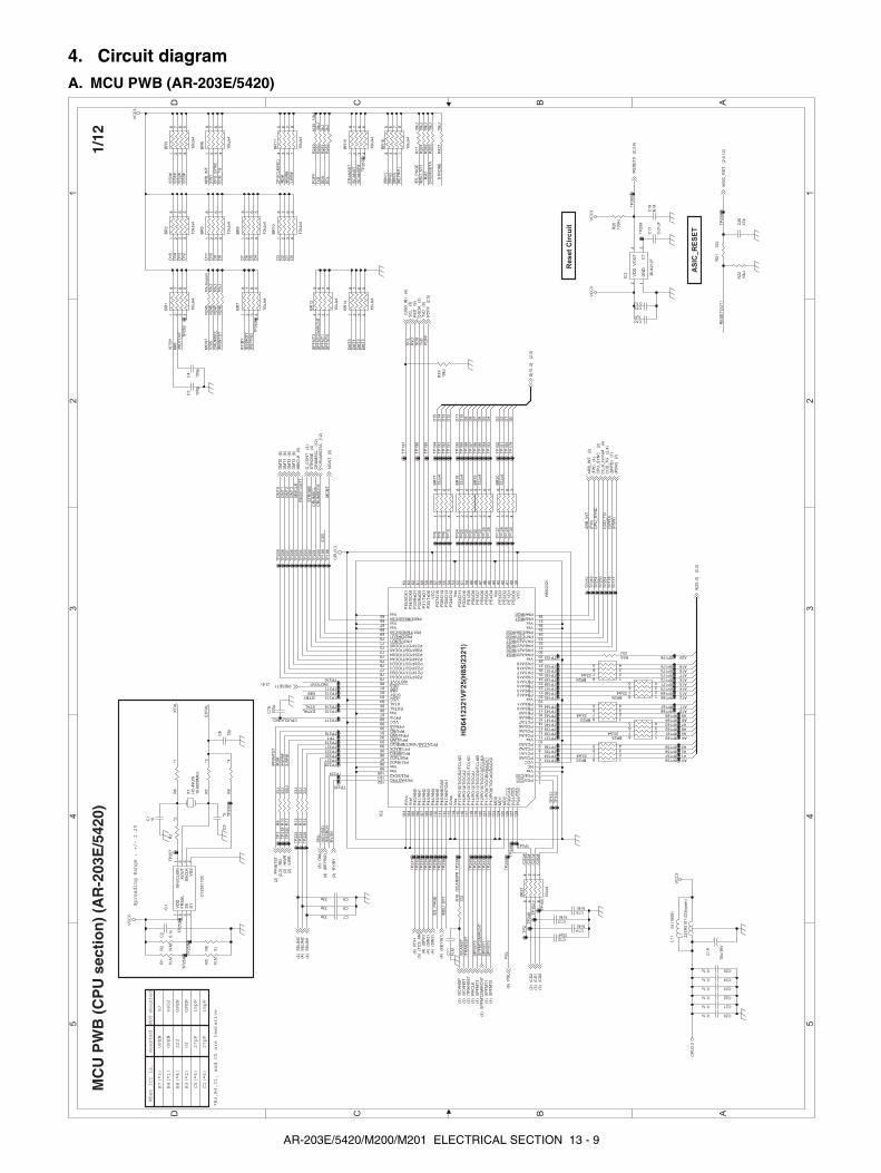
4. Circuit diagramA. MCU PWB (AR-203E/5420)
(SIN
2)
/STBY
/CS
3#
DM
T3
D2
AR
B_IN
T
(SP
PD
)
/WDTOVF
D7
ON
L
AR
B_IN
T
/WD
TO
VF
/CS
5
SC
L
D6
/CS
2#
DM
T2
(SIN
3)
SD
A
D4
/SC
AN
ST
/SC
AN
SP
#
NMI
D2
D10
/ST
BY
/CS
1#
D5
D3
/CS
0#
/CS
3#
DM
T0
A20
D10
CC
D_T
G
SP
FM
T1
/RD
#
D4
(FW
)
D11
D8
(KE
YIN
1)
D8
/LW
R#
D3
D0
/HW
R#
D15
D5
/CS
1#
/SC
AN
ST
PO
FF
/TR
AN
SS
TD
9
SP
FM
T3
/LW
R#
D1
CP
U_S
YN
C
/HW
R#
D9
SP
FM
T2/M
IRC
NT
D6
(SIN
1)
D11
A12
CP
U_S
YN
C
D13
/SC
AN
SP
#
/CS
0#
/RD
#
DM
T1
/TR
AN
SS
T
D1
MC
NT
A8
CP
UC
LK
(NC
)
NM
I
(FW
)
D14
D12
D0
SP
FM
T0
D7
SP
FM
T1
SP
FM
T3
SP
FM
T0
SP
FM
T2/M
IRC
NT
/ES
SR
DY
RY
/BY
CR
UM
SC
L/P
RIN
TS
T
EX
TA
L
XT
AL
(KE
YIN
2)
/PR
INT
ST
TxD
SD
AR
xD
SC
L
PO
FF
/ES
_P
AG
E/M
SU
_S
T1
MC
NT
RY
/BY
/ES
SR
DY
(KE
YIN
2)
TxD R
xD
CR
UM
SD
TA
RE
SE
TO
UT
1
ST
RO
BE
ST
RO
BE
A0A1A2A3
A4A5A6A7
A9A10A11
A13A14A15A16A17A18A19
(PS
W)
D12
D13
D14
D15
/CS
5C
RU
MS
DT
AC
RU
MS
CL
RE
SE
TO
UT
1M
MC
LK
DM
T3
DM
T2
DM
T1
DM
T0
XTALEXTAL
CPUCLK(NC)
/ES
_P
AG
E
/MS
U_S
T1
PS
L
/CS
2#
CC
D_T
G
VC
C3
CP
U3.3
VC
C3
CP
U3.3
VC
C3
VC
C3
VC
C3
RT
H(5
)
(SIN
2)
(4)S
ELIN
1(4
)
(SIN
3)
(4)
SP
FM
T1
(4)
DM
T0
(6)
(SIN
1)
(4)
/CS
1(3
)
CC
D_T
G(2
,4)
DM
T3
(6)
/CS
0(3
)
D_C
ON
T(4
)
DM
T2
(6)
/LW
R(2
)
D[1
5..0]
(2,3
)
SP
FM
T3
(4)
A[2
0..0]
(2,3
)
/RE
SE
T0
(2,3
,4)
ST
RO
BE
(4)
/TR
AN
SS
T(2
)
CP
U_S
YN
C(2
)
(SP
PD
)(7
)
/RD
(2,3
)
/SC
AN
SP
(2)
AR
B_IN
T(2
)
/RESET1(2,4)
(FW
)(4
)
SE
LIN
3(4
)
SP
FM
T0
(4)
/SC
AN
ST
(2)
DM
T1
(6)
/CS
2(2
)
PM
CLK
(5)
(PS
W)
(7)
/HW
R(3
)
SP
FM
T2/M
IRC
NT
(4)
/AS
IC_R
ST
(2,4
,12)
SE
LIN
2(4
)M
MC
LK
(5)
/PR
INT
ST
(2)
PO
FF
(2,5
)T
xD
(9)
SD
A(3
)R
xD
(9)
SC
L(3
)(U
SB
_IN
)(4
)
(KE
YIN
2)
(4)
(TC
S_A
N)
(5)
(KE
YIN
1)
(4)
RY
/BY
(3)
ON
L(8
)C
RU
MS
DT
A(1
2)
CR
UM
SC
L(1
2)
PS
L(8
)
mt_
at_
hom
e#
(4)
MC
NT
(5)
Reset Circuit
R8(*4)
680J
When IC1 is,
*R3,R4,C1, and C5 are temtative
R7(*3)
15pF
OPEN
15pF
R4(*1)
27pF
0J
OPEN
27pF
C1(*6)
C5(*5)
OPEN
0J
R3(*2)
NOT mounted
OPEN
mounted
22J
ASIC_RESET
Spreading Range : +/- 1.2%
TP
226
TP139 TP162
TP
180
TP
253
C200.1u
TP
201
C250.1u
BR
8
10kJx4
1 2 3 4
8 7 6 5
TP167
R261
10kJ
TP
10
TP
222
TP150TP172
TP
242
BR2233Jx4
1234
8765
TP
185
TP227
BR
10
10kJx4
1 2 3 4
8 7 6 5
TP
181
TP
254
R4
*1
TP140 TP163
TP
202
C26
47p
TP
6
TP168
BR2333Jx4
1234
8765
TP
24
BR
3
10kJx4
1 2 3 4
8 7 6 5
IC2
H8S
/2321
HD6412321VF
25(H8S/2321)
P3
5/S
CK
16
4
P3
4/S
CK
06
3
P3
3/R
xD
16
2
P3
2/R
xD
06
1
P3
1/T
xD
16
0
P3
0/T
xD
05
9
VC
C5
8
PD
7/D
15
57
PD
6/D
14
56
PD
5/D
13
55
PD
4/D
12
54
Vss
53
PD
3/D
11
52
PD
2/D
10
51
PD
1/D
95
0
PD
0/D
84
9
PE
7/D
74
8
PE
6/D
64
7
PE
5/D
54
6
PE
4/D
44
5
Vss
44
PE
3/D
34
3
PE
2/D
24
2
PE
1/D
14
1
PE
0/D
04
0
VC
C3
9
AV
cc
10
3
Vre
f1
04
P4
0/A
N0
10
5
P4
1/A
N1
10
6
P4
2/A
N2
10
7
P4
3/A
N3
10
8
P4
4/A
N4
10
9
P4
5/A
N5
11
0
P4
6/A
N6
/DA
01
11
P4
7/A
N7
/DA
11
12
AV
ss
11
3
Vss
11
4
P1
7/P
O1
5/T
IOC
B2
/TC
LK
D1
15
P1
6/P
O1
4/T
IOC
A2
11
6
P1
5/P
O1
3/T
IOC
B1
/TC
LK
C1
17
P1
4/P
O1
2/T
IOC
A1
11
8
P1
3/P
O1
1/T
IOC
D0
/TC
LK
B1
19
P1
2/P
O1
0/T
IOC
C0
/TC
LK
A1
20
P1
1/P
O9
/TIO
CB
0/D
AC
K1
12
1
P1
0/P
O8
/TIO
CA
0/D
AC
K0
12
2
MD
01
23
MD
11
24
MD
21
25
PG
0/C
AS
12
6
PG
1/C
S3
12
7
PG
2/C
S2
12
8
PG3/CS11
PG4/CS02
Vss3
NC4
VCC5
PC0/A06
PC1/A17
PC2/A28
PC3/A39
Vss10
PC4/A411
PC5/A512
PC6/A613
PC7/A714
PB0/A815
PB1/A916
PB2/A1017
PB3/A1118
Vss19
PB4/A1220
PB5/A1321
PB6/A1422
PB7/A1523
PA0/A1624
PA1/A1725
PA2/A1826
PA3/A1927
Vss28
PA4/A20/IRQ429
PA5/A21/IRQ530
PA6/A22/IRQ631
PA7/A23/IRQ732
P67/CS7/IRQ333
P66/CS6/IRQ234
Vss35
Vss36
P65/IRQ137
P64/IRQ038
P53/ADTRG102
P52/SCK2101
Vss100
Vss99
P51/RxD298
P50/TxD297
PF0/BREQ96
PF1/BACK95
PF2/LCAS/ WAIT/BREQO94
PF3/LWR93
PF4/HWR92
PF5/RD91
PF6/AS90
VCC89
PF7/088
Vss87
EXTAL86
XTAL85
VCC84
STBY83
NMI82
RES81
WDTOVF80
P20/PO0/TIOCA379
P21/PO1/YICOB378
P22/PO2/TIOCC377
P23/PO3/TIOCD376
P24/PO4/TIOCA475
P25/PO5/TIOCB474
P26/PO6/TIOCA573
P27/PO7/TIOCB572
P63/TEND171
P62/DREQ170
P61/TEND0/CS569
Vss68
Vss67
P60/DREQ0/CS466
Vss65
TP173
TP
245
TP
243
TP151
TP
261
TP228
R252
2kJ
TP
186
TP141
BR2433Jx4
1234
8765
TP
182
TP
203
BR
6
10kJx4
1 2 3 4
8 7 6 5
TP
131
TP
154
TP
195
TP
8
C2
0.1
u
TP169
TP
25
C160.1u
R17
10kJ
BR2533Jx4
1234
8765
TP
244
TP152TP174
TP
246
R12
33J
TP142
R262
10kJ
C4
100p
TP210
TP
187
TP229
TP
183
TP
155
TP
255
TP
204
TP
132
TP
196
R8
*4
BR2633Jx4
1234
8765
TP170
R250
10kJ
BR
11
10kJx4
1234
8765
R13
33J
R2
N.M
.
TP
258
TP175
TP247
R248
10kJ
TP153
C1222pF
TP211
BR
17
33Jx4
1 2 3 4
8 7 6 5
TP
235
TP143
C14N.M.
TP230
TP
188
BR
7
10kJx4
1 2 3 4
8 7 6 5
TP
184
TP
256
C13N.M.
TP
205
TP133 TP156
C6
12p
TP
197
C15N.M.
IC3 BU
4212F
GN
D1
VD
D2
CT
3
VO
UT
4
R1633J
BR
18
33Jx4
1 2 3 4
8 7 6 5
R263
10kJ
R22
10kJ
BR
15
10kJx4
1 2 3 4
8 7 6 5
R14
33J
TP
259
R246
10kJ
TP
1
TP
126
R1
N.M
.
TP176
TP
248
TP
236
TP144
TP212
TP
189
R21
33J
TP
231
BR
19
33Jx4
1 2 3 4
8 7 6 5
TP
262
X1
HC
-49U
/S19.6
608M
Hz
BR
12
10kJx4
1234
8765
TP134 TP157
TP
257
TP
206
TP
198
C210.1u
TP
193
TP
30
TP7
BR
20
33Jx4
1 2 3 4
8 7 6 5
TP
260
R19
10kJ
C220.1u
TP
177
TP
2
TP
127
TP
267
TP145
R3
*2
TP213
TP
237
R5
N.M
.
TP
190
TP
232
R9
33J
BR
21
33Jx4
1234
8765
TP
263
TP
207
C230.1u
TP135 TP158
TP
199
R421
10kJ
C733p
C101uF
TP
194
TP
31
C78
100p
R245
10kJ(o
pen)
C240.1u
C17
0.0
1uF
TP
218
TP
128
+C
19
10u/1
6V
TP
250
TP
238
TP146
TP214
TP
191
TP
233
TP223
TP
208
TP136 TP159
R6
0J
R7
*3
C833p
C5
*5
C3
100p
BR
1
10kJx4
1 2 3 4
8 7 6 5
R251
2kJ
C933p
TP164
TP
32
TP219
L11
0J (
1608)
TP
251
TP
129
TP
239
TP147
TP215
TP
192
TP
234
TP
224
BR
14
10kJx4
1 2 3 4
8 7 6 5
TP160
TP
178
TP
249
TP
209
TP137
R20
100kJ
R249
N.M
._10kJ
TP165
TP
33
R11
100J
L1
ZJS
R5101-2
23(o
pen)
TP
220
TP
130
TP216
TP
240
TP148
BR
16
10kJx4
1234
8765
TP225
R18
33J
TP
252
TP138 TP161
TP
179
IC1
CY
25811S
C
XIN
/CL
KIN
1
XO
UT
8V
DD
7
VS
S2
SS
CL
K5
FR
SE
L6
S0
4
S1
3
TP
200
BR
2
10kJx4
1 2 3 4
8 7 6 5
R247
10kJ
TP166
C18
N.M
.
TP
125
C1
*6
TP
9
TP221
R10
33J
TP
241
TP149
TP217
BR
5
10kJx4
1 2 3 4
8 7 6 5
TP171
C11
N.M
.
5 5
4 4
3 3
2 2
1 1
DD
CC
BB
AA
MC
U P
WB
(C
PU
sec
tio
n)
(AR
-203
E/5
420)
1/12
AR-203E/5420/M200/M201 ELECTRICAL SECTION 13 - 9
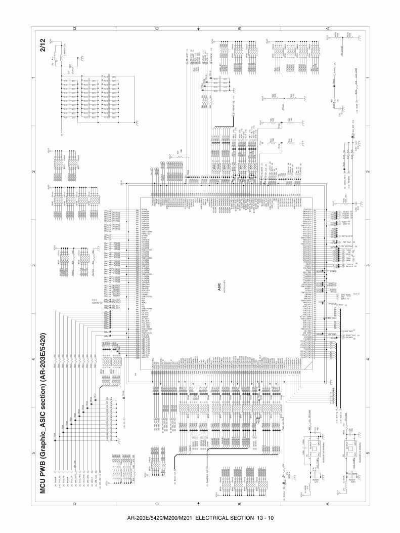
PF
CL
KIN
PFCLKOUT
/IN
RE
Q
SY
NC
#
AF
E_
DB
0
AF
E_
DB
7
AF
E_
DB
4A
FE
_D
B5
AF
E_
DB
6
AF
E_
DB
1A
FE
_D
B2
AF
E_
DB
3
/OU
TA
CK
/PC
LP
RO
/FA
XP
RO
/ES
PR
D
CL
K_
CO
NT
/OU
TC
S
MM
_B
I1
MM
_A
I0M
M_
BI2
MM
_B
I0
MM
_A
I2M
M_
AI1
/AU
TO
FD
/SL
CT
IN/I
NIT
/ST
B
PA
RA
D7
PA
RA
D3
PA
RA
D4
PA
RA
D5
PA
RA
D6
PA
RA
D1
PA
RA
D2
PA
RA
D0
VM
IN
RC
VV
PIN
AF
E_
DB
7A
FE
_D
B6
AF
E_
DB
3
AF
E_
DB
5
AF
E_
DB
2A
FE
_D
B1
AF
E_
DB
4
AF
E_
DB
0
AF
E_
SD
I
RA
MD
B0
RA
MD
B3
RA
MD
B2
RA
MD
B1
RA
MD
B5
RA
MD
B4
RA
MD
B7
RA
MD
B6
RA
MD
B1
2
RA
MD
B1
4R
AM
DB
15
RA
MD
B1
3
RA
MD
B8
RA
MD
B9
RA
MD
B1
0R
AM
DB
11
VM
IN
JT
G_
TD
IJT
G_
TM
SJT
G_
TC
K
PF
CL
K
JT
G_
TD
O
/PIR
EQ
/PO
AC
K
PO
DA
TA
3P
OD
AT
A2
PO
DA
TA
1P
OD
AT
A0
PO
DA
TA
7P
OD
AT
A6
PO
DA
TA
5P
OD
AT
A4
ME
M_
INT
CL
KS
W
CL
K_
CO
NT
CL
K_
CO
NT
SF
CL
K4
8
AF
E_
SD
I
MT
AD
0M
TA
D1
MT
AD
2M
TA
D3
MT
AD
4M
TA
D5
MT
AD
6M
TA
D7
/AU
TO
FD
/SL
CT
IN/I
NITSL
CT
PE
BU
SY
/AC
K
FA
UL
T/R
EV
PA
RA
D7
PA
RA
D6
PA
RA
D5
PA
RA
D4
PA
RA
D3
PA
RA
D2
PA
RA
D1
PA
RA
D0
MM
_B
I0
MM
_A
I0M
M_
AI1
MM
_A
I2
PO
DA
TA
1
PIDATA4
MTAD1
/PCLPRO
A7
D1
/INREQ
A1
PF
CL
KO
UT
CLKSW
PO
DA
TA
0
/PIR
EQ
MTAD8
MTAD12
A5
D6
JTG_TMS
MTAD0
/OUTACK
A2
D0
D7P
OD
AT
A3
SFCLK48
D10
D12
PIDATA0
MTAD7
MTAD11
A8
D5
D15
A6
VP
IN
PO
DA
TA
6
/PO
AC
K
/OUTCS
D14
PO
DA
TA
5
PO
DA
TA
2
PIDATA1
MTAD4
MTAD10SYNC#
JTG_TCK
JTG_TDI
PIDATA5
RAM_CLK_OUT
MTAD15
MM
_B
I2
PFCLK
D9D8
PIDATA2
MTAD3
RC
V
JTG_TDO
PIDATA6
A3
A9
D2
MTAD5
MTAD14
MM
_B
I1
PIDATA3
MTAD2
D3
D11
D13
PO
DA
TA
7
PO
DA
TA
4
PIDATA7
/ESPRD
MEM_INT
/ST
B
PFCLKIN
MTAD6
MTAD9
MTAD13
/FAXPRO
A4
D4
RA
M_
CL
K_
OU
T
MA
D3
MA
D2
MA
D1
MA
D0
MA
D1
0
MA
D1
2M
AD
11
MA
D9
MA
D8
MA
D7
MA
D6
MA
D5
MA
D4
RA
MD
B7
RA
MD
B6
RA
MD
B5
RA
MD
B4
RA
MD
B3
RA
MD
B2
RA
MD
B1
RA
MD
B0
RA
MD
B1
5R
AM
DB
14
RA
MD
B1
3R
AM
DB
12
RA
MD
B1
1R
AM
DB
10
RA
MD
B9
RA
MD
B8
MT
AD
8M
TA
D9
MT
AD
10
MT
AD
11
MT
AD
12
MT
AD
13
MT
AD
14
MT
AD
15
PID
AT
A0
PID
AT
A1
PID
AT
A2
PID
AT
A3
PID
AT
A4
PID
AT
A5
PID
AT
A6
PID
AT
A7
G3
.3V
VC
C3
VC
C3
VC
C3
VC
C3
VC
C3
VC
C3
G3
.3V
VC
C3
VC
C3
VC
C3
VC
C3
VC
C3
VC
C3
VC
C3
VC
C3
VC
C3
VC
C3
VC
C3
MM
_Y
2(5
)
/SD
WD
E(3
)
CC
D_
CP
(4)
HL
(5)
(/S
YN
C)
(4)
MRPS2 (5)
VFM_24V (5)
DQ
M1
(3)
/LWR (1)
TM
(4)
VFMCNT_12V (5)
MM
_Y
1(5
)
/LEND (5)
CC
D_
TG
(1,4
)
MC (5)
PR
(5)
/SC
AN
SP
(1)
BIAS (5)
MM
_P
H_
B(6
)
VS
AM
P(4
)
RRS (5)
MP
FS
(5)
CPFS1 (5)
/SD
RA
S(3
)
MM
_Y
3(5
)
CC
D_
PH
I1(4
)
/CS2 (1)
/RD (1,3)
MMD (5)
SD
CL
K(3
)
MM
_P
H_
A(6
)
TM
_(4
)
VIDEO# (4)
TC (5)
MM
_B
I0(6
)
AF
E_
SC
K(4
)
D[1
5..
0]
(1,3
)
MIRCNT(4)
CC
D_
PH
I2(4
)
PTPULSE (5)
/SD
CS
(3)
MM
_A
I0(6
)
OP
_L
AT
CH
(4)
CL
(10
)
MA
D[1
2..
0]
(3)
BA
NK
0(3
)
MM
_B
I1(6
)
LDEN (5)
/RESET0
(1,3,4)
A[2
0..
0]
(1,3
)
RA
MD
B[1
5..
0]
(3)
CP
FS
2(5
)
/TR
AN
SS
T(1
)
SD
CK
E(3
)
AF
E_
SE
N(4
)
MRPS3 (5)
MIR
ON
(4)
/ASIC_RST (1,4,12)
OP
_C
LK
(4)
MRPS1 (5)
BS
AM
P(4
)
GRIDL(5)
SP
FO
N(4
)
MM
_A
I1(6
)
DQ
M0
(3)
OP
_D
AT
A(4
)
CC
D_
RS
(4)
PMD (5)
/SD
CA
S(3
)
AD
CL
K(4
) AF
E_
DB
[7..
0]
(4)
VP
OU
T(1
1)
VM
OU
T(1
1)
OE
N(1
1)
SU
SP
EN
D(1
1)
VM
IN(1
1)
/PR
INT
ST
(1)
VP
IN(1
1)
RC
V(1
1)
/SC
AN
ST
(1)
AF
E_
SD
I(4
)
PO
FF
(1,5
)
PA
RA
D[7
..0
](1
3)
/RE
V(1
3)
/FA
UL
T(1
3)
/AC
K(1
3)
BU
SY
(13
)P
E(1
3)
SL
CT
(13
)
/IN
IT(1
3)
/SL
CT
IN(1
3)
/AU
TO
FD
(13
)
/OA
_R
ST
(13
)
(/A
SIC
_R
ST
)(4
)
/RE
SE
T1
(1,4
)
CPU_SYNC (1)
/ST
B(1
3)
ARB_INT(1)
BA
NK
1(3
)
R2
43
3J
TP
38
5
TP
33
8
TP274
TP
40
5
TP327
BR
30
10
kJx4
1 2 3 4
8 7 6 5
R2
93
3J
TP
35
6
TP
35
2
TP281
TP
38
8
R5
11
0kJ
TP
42
9
TP
11
2
1
TP
30
8
C4
8
47
p
TP80
1
R5
0N
.M.
TP
34
TP
34
6
C680.1u
TP110
1
C640.1u
TP
36
7
TP
37
7
C600.1u
TP
37
1
TP335
TP96
1
TP
30
2
BR
29
0Jx4
1 2 3 4
8 7 6 5
TP
40
6
TP
44
7
TP79
1
TP
47
1
TP
65
1
TP275
R3
33
3J
TP328
BR
53
10
kJx4
1 2 3 4
8 7 6 5
TP282
R3
81
0kJ
TP109
1
TP4
TP
11
6
1
R4
13
3J
TP
38
9
TP
41
0
TP
33
9
TP
43
0
TP276
TP
39
9
TP
36
8
BR
61
33
Jx4
1 2 3 4
8 7 6 5
C590.1u
C340.1u
BR
48
10
kJx4
1 2 3 4
8 7 6 5
BR
60
33
Jx4
1 2 3 4
8 7 6 5
TP
35
3
TP95
1
TP78
1
R3
13
3J
R3
03
3J
TP
31
1
TP108
1
TP
70
1
TP
37
8
TP294
TP
42
1
TP
5
TP
73
1
TP
12
1
1
TP
34
7
TP
39
1
BR
63
33
Jx4
1 2 3 4
8 7 6 5
TP336
C660.1u
TP
42
3
TP
30
3
TP
39
2
TP
40
7
TP
43
2
TP
56
1
TP
44
8
TP
44
2
R3
23
3J
TP94
1
TP283
BR
34
33
Jx4
1 2 3 4
8 7 6 5
R3
63
33
J
TP
58
1
TP
39
0
TP
54
1
C310.1u
TP
43
1
TP277
TP107
1
TP297
BR
67
10
kJx4
1234
8765
TP279
BR
66
10
kJx4
1234
8765
TP
41
1C5
2
47
p
BR
45
10
kJx4
1 2 3 4
8 7 6 5
TP
76
1
TP
45
1
BR
47
82
Jx4
1 2 3 4
8 7 6 5T
P4
00
TP
36
9
C73N.M.
C2
56
N.M
.
TP
35
4
TP
31
2
TP
34
0
C5
5
47
p
TP295
TP93
1
TP
37
9
R3
75
N.M
.
R2
54
10
kJ
TP
60
1
TP
52
1
TP337
TP106
1
TP285
TP
42
4
R4
8N
.M.
C430.1u
BR
43
10
kJx4
1 2 3 4
8 7 6 5
TP
43
6
TP
67
1
TP
43
3
TP
45
1
R4
91
0kJ
BR
36
33
Jx4
1 2 3 4
8 7 6 5
TP
39
3
R5
33
3J
R3
41
0K
J TP284
TP
44
3
TP
44
9
TP
39
1
TP280
R4
09
N.M
._1
0K
J
TP
41
2
TP92
1
TP
36
TP
40
1
TP
37
0
BR
28
10
kJx4
1234
8765
TP
35
5
TP105
1
C670.1u
C290.1u
TP
35
7
TP
31
3
TP296
TP
50
1
X3
SG
80
02
DC
(18
.38
56
MH
z)
N.C
.1
VC
C8
OU
TP
UT
5
GN
D4
TP
62
1
TP
36
0
C270.1u
BR
52
10
kJx4
1 2 3 4
8 7 6 5
C460.1u
TP286
TP
42
5
R2
33
3J
TP
43
7
TP
34
1
TP91
1
R2
36
N.M
.
TP
39
4
TP
43
4
BR
68
10
kJx4
1234
8765
TP
44
4
X2
SG
80
02
DC
(48
.00
00
MH
z)
N.C
.1
VC
C8
OU
TP
UT
5
GN
D4
TP104
1
TP
12
0
1
R3
74
N.M
.
TP
31
6
C320.1u
TP
41
3
C280.1u
TP292
TP3
TP
40
2
C300.1u
TP90
1
TP
35
8
TP
31
4
C5
4
47
p
TP
40
1
C5
0
47
p
TP103
1
TP
36
1
TP
37
1
BR
35
33
Jx4
1 2 3 4
8 7 6 5
TP
38
1
TP271
TP77
1
TP
43
8
TP
72
1
C2
31
12
0p
TP
42
6
L1
2N
.M.
TP268
TP
39
5
R2
55
10
kJ
TP
43
5
TP329
R4
04
33
J
TP
12
4
1
BR
51
10
kJx4
1 2 3 4
8 7 6 5
TP89
1
C5
8
N.M
.
TP
38
0
BR
62
33
Jx4
1 2 3 4
8 7 6 5
TP
44
5
R5
2
10
J
BR
27
10
kJx4
1234
8765
C2
57
47
p
TP
34
2
TP
64
1
TP
31
7
TP
48
1
TP
41
4
TP288
BR
40
33
Jx4
1 2 3 4
8 7 6 5
TP102
1
TP293
C23222000p
BR
41
33
Jx4
1 2 3 4
8 7 6 5T
P4
3
1
TP
69
1
R2
56
10
kJ
TP
41
5
TP
75
1
TP290
C350.1u
TP
31
5
TP
45
2
TP
35
9
TP88
1
C630.1u
C470.1u
TP272
TP
36
2
TP
37
2
TP
42
7
TP269
TP
43
9
TP101
1
C4
9
47
p
TP330
BR
42
10
kJx4
1 2 3 4
8 7 6 5
BR
39
10
kJx4
1 2 3 4
8 7 6 5
TP
39
6
TP323
TP
38
1
BR
71
10
kJx4
1 2 3 4
8 7 6 5
TP
34
8
TP
31
8
TP289
TP87
1
BR
54
10
kJx4
1 2 3 4
8 7 6 5
TP
11
5
1
R4
07
N.M
.
BR
37
33
Jx4
1 2 3 4
8 7 6 5
L2
ZJS
R5
10
1-2
23
TP
30
9
R4
73
3J
TP
30
4
TP
11
9
1
TP100
1
TP291
C5
1
47
p
TP
41
6
TP
44
6
R2
73
3J
C420.1u
TP
34
3
+C
37
47
u/1
6V
R2
81
0K
J
C650.1u
TP
36
3
TP
37
3
C380.1u
C330.1u
TP
44
0
TP86
1
C71N.M.
TP
39
7
TP
46
1
TP331
TP
66
1
TP
55
1
TP99
1
TP
38
2
TP
57
1
IC4
HG
73
C1
41
HF
V
ASIC
CPU_DATA71
CPU_DATA62
CPU_DATA53
CPU_DATA44
CPU_DATA18
CPU_DATA36
CPU_DATA27
VCC(AC)5
CPU_DATA09
GND(AC)10
MIRCNT11
/CPUSYNC12
MEM_INT13
ARB_INT14
VCC(CORE)15
CPU_AD816
CPU_AD717
CPU_AD618
CPU_AD519
GND(CORE)20
RAM_CLK_IN21
CPU_AD422
CPU_AD323
CPU_AD224
CPU_AD125
CPU_AD026
/CPUCS27
SFCLK4828
GND(CORE)29
/CPUWR30
/CPURD31
/RESET32
PFCLK34
CLKSW35
GND(CORE)36
PFCLKOUT37
PFCLKIN38
GND(PLL)39
VCC(PLL)40
GND(PLL)41
VCC(PLL)42
TM2_15M43
/SYNC44
GND(AC)45
/VIDEO46
/LEND47
VCC(AC)48
OUTP00A49
OUTP02A51
OUTP03A52
OUTP04A53
OUTP05A54
OUTP06A55
VCC(CORE)57
OUTP15A56
OUTP07A58
OUTP08A59
GND(CORE)60
OUTP09A61
OUTP10A62
OUTP11A63
OUTP12A64
VC
C(C
OR
E)
86
OU
TP
13
B8
4
OU
TP
12
B8
3
OU
TP
10
B8
1
GND(AC)69
OU
TP
09
B8
0
OU
TP
08
B7
9
OUTP03B72
GN
D(C
OR
E)
78
OU
TP
07
B7
7
OU
TP
06
B7
6
OUTP00B68
OUTP14A67
VCC(CORE)66
OUTP13A65
VCC(AC)74
OUTP04B73
OU
TP
11
B8
2
OUTP02B71
OU
TP
05
B7
5
OU
TP
14
B8
5
OUTP01B70
TS
P_
MO
DE
96
OP
E_
CL
K9
2
/TM
87
TM
88
OP
E_
DA
TA
89
OP
E_
LA
TC
H9
0G
ND
(AC
)9
1
VC
C(A
C)
93
/SC
AN
SP
94
TS
O0
95
IE1
28
4_
ST
B9
7IE
12
84
_A
UT
OF
D9
8V
CC
(CO
RE
)9
9IE
12
84
_S
LC
TIN
10
0IE
12
84
_IN
IT1
01
IE1
28
4_
SL
CT
10
2G
ND
(CO
RE
)1
03
IE1
28
4_
PE
10
4IE
12
84
_B
US
Y1
05
IE1
28
4_
AC
K1
06
IE1
28
4_
FA
UL
T1
07
VC
C(C
OR
E)
10
8IE
12
84
_R
EV
10
9IE
12
84
_P
AR
AD
71
10
IE1
28
4_
PA
RA
D6
11
1IE
12
84
_P
AR
AD
51
12
IE1
28
4_
PA
RA
D4
11
3IE
12
84
_P
AR
AD
31
14
IE1
28
4_
PA
RA
D2
11
5V
CC
(AC
)1
16
IE1
28
4_
PA
RA
D1
11
7IE
12
84
_P
AR
AD
01
18
SU
SP
EN
D1
19
GN
D(A
C)
12
0O
EN
12
1V
MO
UT
12
2V
PO
UT
12
3G
ND
(CO
RE
)1
24
VM
IN1
25
VP
IN1
26
RC
V1
27
/SC
AN
ST
12
8
VCC(CORE)192
/INREQ191
/OUTCS190
/OUTACK189
/ESPRD188
/FAXPRD187
/PCLPRD186
GND(AC)185
MDAT15184
MDAT14183
MDAT13182
VCC(CORE)181
MDAT12180
MDAT11179
MDAT10178
VCC(AC)177
MDAT09176
MDAT08175
MDAT07174
GND(CORE)173
MDAT06172
MDAT05171
MDAT04170
VCC(CORE)169
MDAT03168
MDAT02167
MDAT01166
MDAT00165
GND(AC)164
/INCS163
/INACK162
/OUTREQ161
GND(CORE)160
/HSYNC159
PIDATA0158
PIDATA1157
PIDATA2156
VCC(AC)155
PIDATA3154
PIDATA4153
PIDATA5152
PIDATA6151
PIDATA7150
/POCS149
/PO
RE
Q1
48
VC
C(A
C)
14
7
/PIW
T1
46
/PIA
CK
14
5
GN
D(A
C)
14
4
/PO
AC
K1
43
/PIR
EQ
14
2
GN
D(C
OR
E)
14
1
PO
DA
TA
01
40
PO
DA
TA
11
39
PO
DA
TA
21
38
PO
DA
TA
31
37
PO
DA
TA
41
36
PO
DA
TA
51
35
PO
DA
TA
61
34
PO
DA
TA
71
33
VC
C(C
OR
E)
13
2
/TR
AN
SS
T1
31
/RE
CE
PT
ST
13
0
/PR
INT
ST
12
9
RA
M_
DA
TA
42
56
RA
M_
DA
TA
52
55
RA
M_
DA
TA
62
54
RA
M_
DA
TA
72
53
GN
D(A
C)
25
2R
AM
_D
QM
02
51
RA
M_
WD
E2
50
VC
C(A
C)
24
9R
AM
_C
AS
24
8R
AM
_R
AS
24
7R
AM
_C
S2
46
RA
M_
BA
NK
S0
24
5R
AM
_B
AN
KS
12
44
VC
C(C
OR
E)
24
3R
AM
_M
AD
10
24
2R
AM
_M
AD
02
41
RA
M_
MA
D1
24
0G
ND
(CO
RE
)2
39
RA
M_
MA
D2
23
8R
AM
_M
AD
32
37
GN
D(A
C)
23
6M
M_
AI2
23
5M
M_
AI1
23
4M
M_
AI0
23
3M
M_
PH
_A
23
2
AFE_DB3217
MM
_B
I22
31
MM
_B
I12
30
MM
_Y
22
25
VCC(AC)221
MM
_Y
12
26
AFE_DB0220
AFE_DB1219
GN
D(C
OR
E)
22
3
AFE_DB2218
AFE_DB4216
AFE_DB5215
MM
_B
I02
29
MM
_P
H_
B2
28
VC
C(C
OR
E)
22
7
MM
_Y
32
24
CLPWM222
AFE_DB6214
AFE_DB7213
GND(AC)212
AFESCK211
VCC(CORE)210
ADCLK209
GND(CORE)208
AFE_SEN207
CCD_PH1206
CCD_PH2205
AFE_SDI204
CCD_CP203
BSAMP202
CCD_RS201
CCD_TG200
VSAMP199
GND(CORE)198
TD0197
TRSK195
TDI196
TCK193
TMS194
VCC(CORE)33
OUTP01A50
GN
D(C
OR
E)
25
7
RA
M_
DA
TA
32
58
RA
M_
DA
TA
22
59
RA
M_
DA
TA
12
60
RA
M_
DA
TA
02
61
GN
D(A
C)
26
2
RA
M_
DA
TA
15
26
3
RA
M_
DA
TA
14
26
4
VC
C(C
OR
E)
26
5
RA
M_
DA
TA
13
26
6
RA
M_
DA
TA
12
26
7
RA
M_
DA
TA
11
26
8
RA
M_
DA
TA
10
26
9
RA
M_
DA
TA
92
70
RA
M_
DA
TA
82
71
VC
C(C
OR
E)
27
2
RA
M_
DQ
M1
27
3
RA
M_
CK
E2
74
GN
D(A
C)
27
5
RA
M_
CL
K_
OU
T2
76
GN
D(C
OR
E)
27
7
RA
M_
MA
D1
22
78
RA
M_
MA
D1
12
79
RA
M_
MA
D9
28
0
VC
C(C
OR
E)
28
1
RA
M_
MA
D8
28
2
RA
M_
MA
D7
28
3
VC
C(A
C)
28
4
RA
M_
MA
D6
28
5
RA
M_
MA
D5
28
6
RA
M_
MA
D4
28
7
GN
D(A
C)
28
8
CP
UD
AT
A1
52
89
CP
UD
AT
A1
42
90
CP
UD
AT
A1
32
91
CP
UD
AT
A1
22
92
CP
UD
AT
A1
12
93
CP
UD
AT
A1
02
94
CP
UD
AT
A9
29
5
CP
UD
AT
A8
29
6
C610.1u
TP324
C450.1u
TP
34
9
TP
31
9
TP
12
3
1
C7
4N
.M.
TP
30
5
R3
53
3J
C2
64
10
00
p
R2
63
3J
TP
31
0
BR
70
10
kJx4
1 2 3 4
8 7 6 5
TP
42
0
TP
53
1
TP
41
7
TP85
1
BR
44
33
Jx4
1 2 3 4
8 7 6 5
TP
59
1
R2
53
10
kJ
R4
03
33
J
TP287
BR
46
10
kJx4
1 2 3 4
8 7 6 5
TP98
1
R4
23
3J
TP
37
4
TP
32
0
TP
36
4
TP
40
8
R2
53
3J
TP
44
1
TP
34
4
TP332
L1
00
J (
16
08
)
TP
39
8
R4
5N
.M.
TP
40
3
TP325
TP84
1
TP
38
3
TP
41
1
TP
35
0
C360.1u
TP
71
1
BR
31
0Jx4
1 2 3 4
8 7 6 5
TP
38
6
TP
51
1
TP97
1
TP
61
1
TP
30
6
C5
3
N.M
.
TP
45
0
TP
42
1
R3
9
10
kJ
TP
41
8
TP
29
8
TP
11
4
1
BR
50
33
Jx4
1 2 3 4
8 7 6 5
C390.1u
TP278
TP
11
8
1
R4
41
0kJ
TP
74
1
BR
69
10
kJx4
1234
8765
TP83
1
BR
32
10
kJx4
1 2 3 4
8 7 6 5
R3
61
0kJ
C7
9 47
pR
40
63
3J
TP
36
5
BR
33
10
kJx4
1 2 3 4
8 7 6 5
TP
37
5
TP
32
1
C72N.M.
TP
11
3
1
TP
40
9
C7522000p
R4
03
3J
TP
30
0
C70N.M.
R3
71
0kJ
TP
11
7
1
TP333
BR
49
33
Jx4
1 2 3 4
8 7 6 5
TP
38
4
TP273
TP
40
4
TP326
TP
68
1
TP
44
1
TP
35
1
R4
08
N.M
.
C440.1u
C400.1u
TP
38
7
TP
34
5
TP82
1
L1
30
J (
16
08
)
TP
42
8
TP
30
7
TP
35
TP
42
2
TP
63
1
TP
41
9
TP
49
1
TP
12
2
1
C7
78
2p
C410.1u
C690.1u
TP
29
9
C2300.1u
TP
36
6
TP
37
6
TP
32
2
C5
6
N.M
.
C7
60
.1u
R4
33
3J
TP81
1
C5
7
47
p
C620.1u
TP334
TP111
1
TP
30
1
5 5
4 4
3 3
2 2
1 1
DD
CC
BB
AA
MC
U P
WB
(G
rap
hic
_AS
IC s
ecti
on
) (A
R-2
03E
/542
0)2/
12
AR-203E/5420/M200/M201 ELECTRICAL SECTION 13 - 10
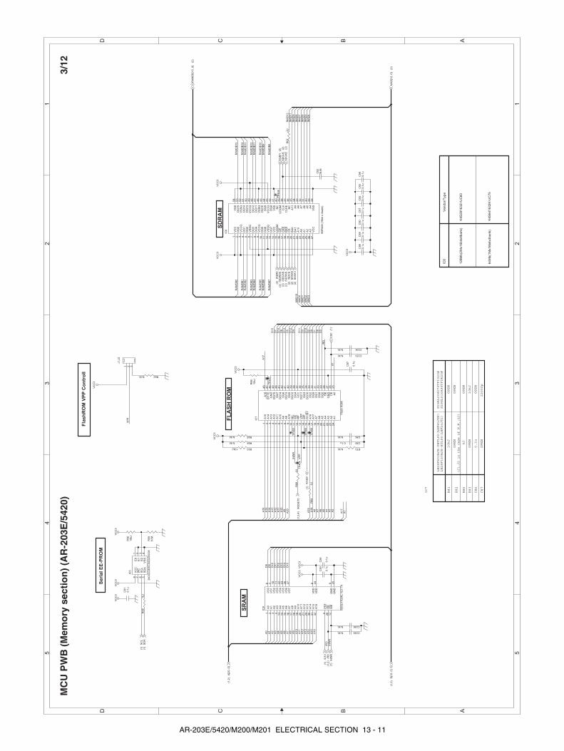
D6
/HW
R
RA
MD
B14
D7
A17
A4
RA
MD
B5
A8
MA
D9
/HW
R
MA
D1
A5
A2
A7
A14
MA
D6
D0
D2
D8
RA
MD
B9
RA
MD
B13
A15
A3
A2
RA
MD
B3
D15
MA
D8
VP
P
MA
D12
A8
A11
D13
D11
A15
VP
P
D3
D10
D14
A13
A19
A13
RA
MD
B12
D10
RA
MD
B8
MA
D2
D14
RA
MD
B4
MA
D7
D15
MA
D11
A10
D9
A16
A18
D11
A12
MA
D3
A1
RA
MD
B11
D5
A16
RA
MD
B7
A1
A14
MA
D10
RA
MD
B2
D9
MA
D5
D8
RA
MD
B10
A7
A5
RA
MD
B0
A3
A9
D1
A1
A6
D12
RA
MD
B15
A10
A9
MA
D0
/RD
RA
MD
B6
A6
D4
MA
D4
RA
MD
B1
A12
A0
A4
A11
A17
D13
D12
A20
/RD
VC
C3
VC
C3
VC
C3
VC
C3
VC
C3
VC
C3
VC
C3
VC
C3
VC
C3
VC
C3
VC
C3
D[1
5..0]
(1,2
)
RA
MD
B[1
5..0]
(2)
/CS
1(1
)
/CS
0(1
)
RY
/BY
(1)
/SD
CS
(2)/S
DR
AS
(2)
/RE
SE
T0
(1,2
,4)
MA
D[1
2..0]
(2)
/RD
(1,2
)
/SD
WD
E(2
)D
QM
0(2
)
BA
NK
0(2
)
SD
CLK
(2)
/HW
R(1
)
/SD
CA
S(2
)D
QM
1(2
)
SD
CK
E(2
)
BA
NK
1(2
)
A[2
0..0]
(1,2
)
SC
L(1
)S
DA
(1)
Serial EE-PROM
FlashROM
VPP
Controll
IC6
64M
b(1
Mx16bitx4bank)
K4S
281632I-
UC
60
K4S
641632K
-UC
75
SDRAM V
endor/
Type
128M
b(2
Mx16bitx4bank)
(J1,J2 in the case of N.M.:0J)
0J
R86
10kJ
OPEN
OPEN
R83
OPEN
R82
OPEN
10kJ
OPEN
S29AL008D70TFI020#
S29GL016A90TFIR20#
LH28F800BJE-PBTL90(LHF80JZP)
LH28F160BJE-BTL90(LHF16JT2)
0.1u
IC7
R81
C86
OPEN
22000p
OPEN
C87
FLASH
ROM
SRAM
TP
453
C233N.M.
C234N.M.
IC7
Fla
sh R
OM
A0
25
A1
24
A2
23
A3
22
A4
21
A5
20
A6
19
A7
18
A8
8A
97
A1
06
A1
15
A1
24
A1
33
A1
42
A1
51
A1
64
8
A1
71
7
DQ
02
9
DQ
13
1
DQ
23
3
DQ
33
5
DQ
43
8
DQ
54
0
DQ
64
2
DQ
74
4
DQ
83
0
DQ
93
2
DQ
10
34
DQ
11
36
DQ
12
39
DQ
13
41
DQ
14
43
DQ
15
45
A1
99
NC
10
A1
81
6
GN
D4
6
GN
D2
7
VC
C3
7
VP
P1
3
BY
TE
47
OE
28
CE
26
WE
11
RP
12
WP
14
RY
/BY
15
C89
0.1
u
R56
10kJ
R65N.M.
TP
454
C90
0.1
uC
91
0.1
u
TP
458
C92
0.1
uC
93
0.1
u
TP
455
R64N.M.
C84
0.1
u
C81
0.1
u
C94
0.1
u
R68
0J
R69
0J
TP
456
R6310kJ
C86N.M.
C236N.M.
C88
0.1
u
R59
N.M
.
C235N.M.
C82
N.M
.
IC5
24C
02/2
4W
C04/2
4W
C08
E0
1
E1
2
E2
3
VS
S4
SD
A5
SC
L6
WC
7V
CC
8
C850.1u
R66
10kJ
IC6
SD
RA
M (
16bit x
4bank)
A0
23
A1
24
A2
25
A3
26
A4
29
A5
30
A6
31
A7
32
A8
33
A9
34
A1
02
2
BA
02
0
DQ
02
DQ
14
DQ
25
DQ
37
DQ
48
DQ
51
0
DQ
61
1
DQ
71
3D
Q8
42
DQ
94
4D
Q1
04
5
DQ
11
47
DQ
12
48
DQ
13
50
DQ
14
51
DQ
15
53
VC
C1
VC
C2
7
VS
S5
4
VS
S2
8
VC
CQ
9
VS
S4
1
VC
CQ
43
VC
CQ
49
VS
SQ
6
VS
SQ
12
VS
SQ
46
VS
SQ
52
LD
QM
15
UD
QM
39
WE
16
CA
S1
7
RA
S1
8
CS
19
CL
KE
37
CL
K3
8
NC
40
NC
36
VC
CQ
3
VC
C1
4
BA
12
1A
11
35
R67
0J
J1,J
2
1 2 3
IC8
IS63LV
1024L-1
2J-T
R
I/O
06
A0
1
I/O
17
A1
2
I/O
21
0A
23
I/O
31
1A
34
I/O
42
2A
41
3
I/O
52
3A
51
4
I/O
62
6A
61
5
I/O
72
7A
71
6
A8
17
A9
18
A1
01
9
A1
12
0
A1
22
1
A1
32
9
A1
43
0
CS
15
OE
28
WE
12
VD
D8
GN
D9
VD
D2
4A
15
31
A1
63
2
GN
D2
5
R58
1kJ
TP
457
C83
0.1
u
R62N.M.
C87
0.1
u
R70N.M.
5 5
4 4
3 3
2 2
1 1
DD
CC
BB
AA
MC
U P
WB
(M
emo
ry s
ecti
on
) (A
R-2
03E
/542
0)3/
12
AR-203E/5420/M200/M201 ELECTRICAL SECTION 13 - 11
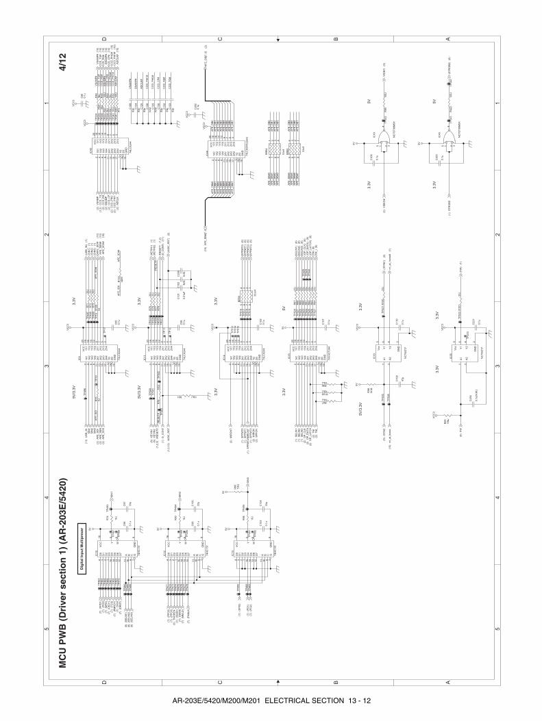
/RE
SE
T#
VS
AM
P#
CC
D_
TG
#C
CD
_R
S#
BS
AM
P#
CC
D_
CP
#C
CD
_P
HI2
#C
CD
_P
HI1
#
AD
CL
K#
/RE
SE
T#
AF
E_
SD
I#A
FE
_S
DI
5 5
4 4
3 3
2 2
1 1
DD
CC
BB
AA
MC
U P
WB
(D
rive
r se
ctio
n 1
) (A
R-2
03E
/542
0)4/
12
AF
E_
SD
I#A
FE
_S
DI
AF
E_
DB
#0
AF
E_
DB
#3
AF
E_
DB
#2
AF
E_
DB
#1
AF
E_
DB
#7
AF
E_
DB
#5
AF
E_
DB
#4
AF
E_
DB
#6
AF
E_
DB
#0
AF
E_
DB
#3
AF
E_
DB
#2
AF
E_
DB
#1
AF
E_
DB
#7
AF
E_
DB
#5
AF
E_
DB
#4
AF
E_
DB
#6
AF
E_
DB
3
AF
E_
DB
7
AF
E_
DB
5A
FE
_D
B4
AF
E_
DB
6
AF
E_
DB
2
AF
E_
DB
0
AF
E_
DB
5
AF
E_
DB
2
AF
E_
DB
1
AF
E_
DB
4
AF
E_
DB
7A
FE
_D
B6
AF
E_
DB
1
AF
E_
DB
0
AF
E_
DB
3
VS
AM
P#
BS
AM
P#
AD
CL
K#
CC
D_
PH
I1#
CC
D_
PH
I2#
CC
D_
CP
#
CC
D_
RS
#
CC
D_
TG
#
VC
C3
5V
5V
5V
5V
5V
5V
VC
C3
5V
VC
C3
VC
C3
VC
C3
VC
C3
5V
VC
C3
VC
C3
VC
C3
VC
C3
SE
LIN
3(1
)
(CE
D1
)(7
)
SIN
2
OP
_L
AT
CH
(2)
KE
YIN
1(8
)
(PD
1)
(7)
(OP
_C
LK
)(8
)
(SP
ID)
(7)
OP
_D
AT
A(2
)
(FW
)(1
)
TM
_(2
)
(DR
ST
)(7
)
(TM
_)
(6)
(TM
)(6
)
(PM
RD
Y)
(7)
/SY
NC
(9)
(CE
D2
)(7
)
(OP
_L
AT
CH
)(8
)
SE
LIN
2(1
)
(PO
D)
(7)
(PP
D3
)(7
)(P
PD
2)
(7)
(TC
S)
(7)
(OP
_D
AT
A)
(8)
(SE
LIN
3)
(8)
(SE
LIN
1)
(8)
/VID
EO
(9)
SIN
1
SE
LIN
1(1
)
(PD
2)
(7)
DS
WS
(7)
/RE
SE
T1
(1,2
)
SIN
1S
IN2
OP
_C
LK
(2)
SIN
3
(MF
D)
(7)
TH
OP
EN
(5)
(PP
D1
)(7
)
(SE
LIN
2)
(8)
TM
(2)
VID
EO
#(2
)
(MM
LD
)(7
)
SIN
3
DV
S1
(7)
FW
(8)
US
B_
IN(1
1)
KE
YIN
2(8
)(K
EY
IN1
)(1
)(K
EY
IN2
)(1
)/R
ES
ET
0(1
,2,3
)
MIR
ON
(2)
SP
FM
T2
/MIR
CN
T(1
)(S
PF
MT
1)
(6)
(SP
FM
T0
)(6
)
SP
FO
N(2
)
MIR
CN
T(2
)
(SP
FM
T2
)(6
)
SP
FM
T0
(1)
(SP
FM
T3
)(6
)S
PF
MT
3(1
)
SP
FM
T1
(1)
(/S
YN
C)
(2)(S
EL
IN2
)(8
)(S
EL
IN1
)(8
)
(SE
LIN
3)
(8)
(US
B_
IN)
(1)
(SIN
1)
(1)
(SIN
3)
(1)
(SIN
2)
(1)
D_
CO
NT
(1)
(D_
CO
NT
)(1
1)
(FA
NL
K)
(7)
/AS
IC_
RS
T(1
,2,1
2)
(/A
SIC
_R
ST
)(2
)
ST
RO
BE
(1)
(ST
RO
BE
)(8
)
mt_
at_
ho
me
(10
)m
t_a
t_h
om
e#
(1)
CC
D_
CP
#(1
0)
CC
D_
TG
#(1
0)
VS
AM
P#
(10
)
CC
D_
PH
I1#
(10
)
AF
E_
SC
K#
(10
)
CC
D_
PH
I2#
(10
)
BS
AM
P#
(10
)C
CD
_R
S#
(10
)
AD
CL
K#
(10
)
AF
E_
SD
I#(1
0)
VS
AM
P(2
)C
CD
_T
G(1
,2)
CC
D_
RS
(2)
BS
AM
P(2
)C
CD
_C
P(2
) CC
D_
PH
I2(2
)C
CD
_P
HI1
(2)
AD
CL
K(2
)
AF
E_
SD
I(2
)A
FE
_S
EN
(2)
AF
E_
SC
K(2
)A
FE
_S
EN
#(1
0)
AF
E_
DB
#[7
..0
](1
0)
AF
E_
DB
[7..
0]
(2)
5V
/3.3
V
3.3
V5V
3.3
V
Digital Input Multiprexer
5V
3.3
V
3.3
V3.3
V
5V
/3.3
V3.3
V
5V
/3.3
V3.3
V
3.3
V3.3
V5V
3.3
V
BR
64
0Jx4
1 2 3 4
8 7 6 5
R9
13
3J
TP
47
2
R12810kJ
C1
32
33
p
TP
49
8
TP
53
9
R9
51
00
J
TP
52
3
R8
83
3J
R4
22
10
0J
C1
03
0.1
u
TP
27
0
C1
09
47
p
TP
49
2
TP
48
0
IC1
5
74
VH
CT
24
4
1A
12
1A
24
1A
36
1A
48
2A
111
2A
213
2A
315
2A
417
1G
1
2G
19
1Y
118
1Y
216
1Y
314
1Y
412
2Y
19
2Y
27
2Y
35
2Y
43
VC
C20
GN
D10
R7
33
3J
IC1
4
74
LC
X2
44
1A
12
1A
24
1A
36
1A
48
2A
111
2A
213
2A
315
2A
417
1G
1
2G
19
1Y
118
1Y
216
1Y
314
1Y
412
2Y
19
2Y
27
2Y
35
2Y
43
VC
C20
GN
D10
BR
55 3
3Jx4
1234
8765
R1
50
J
TP
47
3
R8
6
10
J
IC1
3
74
HC
15
1
D0
4
D1
3
D2
2
D3
1
D4
15
D5
14
D6
13
D7
12
A11
B10
C9
G7
W6
Y5
VC
C16
GN
D8
TP
46
3
TP
49
9
TP
54
0
C9
6
0.1
u
C9
9
0.1
u
R9
03
3J
R1
00
33
J
TP
52
4
C1
04
33
p
C1
33
82
p
R8
73
3J
TP
50
3
R8
0
10
J
R7
4
10
J
TP
50
0
IC4
5
NC
7S
T0
8M
5X
1 2 3
4
5
TP
53
3
C8
00
.1u
R81 10kJ
TP
50
7
C1
00
33
p
TP
47
4TP
46
4
R4
65
6J
TP
51
0
TP
54
1
R1
30
0J
TP
52
5
TP
49
6
C9
7
33
p
TP
52
7
TP
11
IC9
74
LC
X2
44
1A
12
1A
24
1A
36
1A
48
2A
111
2A
213
2A
315
2A
417
1G
1
2G
19
1Y
118
1Y
216
1Y
314
1Y
412
2Y
19
2Y
27
2Y
35
2Y
43
VC
C20
GN
D10
TP
51
3
TP
50
1
TP
49
3
TP
48
2
R8
51
0kJ
R7
93
3J
TP
18
TP
47
5
TP
50
8
C1
02
N.M
.
TP
46
5
R7
81
00
J
C1
08
82
p
TP
51
1
R5
45
6J
TP
48
7
TP
52
6
R1
33
op
en
TP
52
8
TP
51
4
TP
49
4
IC1
6
NC
7S
T0
8M
5X
1 2 3
4
5
R1
01
33
J
TP
48
3
TP
49
7
TP
47
6
TP
50
9TP
19
TP
46
6
TP
48
8
C1
24
82
p
TP
52
9
R5
51
00
J
C2
63
0.1
u
TP
51
5
TP
49
5
TP
48
4
IC1
1
74
LC
X2
44
1A
12
1A
24
1A
36
1A
48
2A
111
2A
213
2A
315
2A
417
1G
1
2G
19
1Y
118
1Y
216
1Y
314
1Y
412
2Y
19
2Y
27
2Y
35
2Y
43
VC
C20
GN
D10
IC1
2
74
HC
15
1
D0
4
D1
3
D2
2
D3
1
D4
15
D5
14
D6
13
D7
12
A11
B10
C9
G7
W6
Y5
VC
C16
GN
D8
TP
46
7
TP
12
TP
48
9
TP
53
4
TP
53
0
TP
50
5
C1
25
82
p
R7
63
3J
TP
51
6
TP
17
TP
48
5
R5
75
6J
TP
46
8C
95
0.1
u
TP
53
5
R9
23
3J
TP
53
1
TP
51
7
TP
48
6
C2
55
N.M
.
TP
54
4
R8
34
7J C
12
6N
.M.
R7
53
3J
C2
58
0.1
u(N
.M.)
IC1
0
74
HC
15
1
D0
4
D1
3
D2
2
D3
1
D4
15
D5
14
D6
13
D7
12
A11
B10
C9
G7
W6
Y5
VC
C16
GN
D8
R7
71
kJ
R6
05
6J
IC1
8
NC
7W
Z1
7
A1
1
A2
3
Y1
6
Y2
4
GN
D2
Vcc
5
C2
21
0.1
u
C9
80
.1u
TP
46
9
BR
65
0Jx4
1234
8765
TP
53
6
TP
52
0
TP
54
2
R9
8N
.M.
TP
51
8
C1
01
0.0
1u
F
IC4
3
74
LC
X2
44
1A
12
1A
24
1A
36
1A
48
2A
111
2A
213
2A
315
2A
417
1G
1
2G
19
1Y
118
1Y
216
1Y
314
1Y
412
2Y
19
2Y
27
2Y
35
2Y
43
VC
C20
GN
D10
C1
10
0.1
u
IC3
5
NC
7W
Z1
7
A1
1
A2
3
Y1
6
Y2
4
GN
D2
Vcc
5
C1
06
0.1
u
C1
29
N.M
.T
P5
02
R6
11
00
J
TP
47
0
C1
05
0.1
u
C2
62
0.1
u
TP
53
7
TP
52
1
R7
13
3J
R9610kJ
TP
51
9
C1
07
0.1
u
TP
54
3
R9
91
0kJ
TP
49
0
TP
50
6
TP
47
7
R9710kJ
TP
47
1
C1
30
82
p
R9
33
3J
R8
93
3J
TP
53
8
R8
21
00
J
TP
52
2
R9
43
3J
IC4
4
74
LC
X2
44
(op
en
)
1A
12
1A
24
1A
36
1A
48
2A
111
2A
213
2A
315
2A
417
1G
1
2G
19
1Y
118
1Y
216
1Y
314
1Y
412
2Y
19
2Y
27
2Y
35
2Y
43
VC
C20
GN
D10
R7
23
3J
TP
49
1
TP
47
8
AR-203E/5420/M200/M201 ELECTRICAL SECTION 13 - 12

/PR
PR
#
PR
#
VC
C3
VC
C3
24
V
VC
C3
VC
C3
5V
12
V
PG
ND
INT
5V
12
V
PG
ND
VC
C3
12
V
12
V
12
V
5V
24
V
12
V5
VV
CC
3
24
V
12
V
PG
ND
24
V
PG
ND
5V
VC
C3
5V
VC
C3
VC
C3
12
V
VC
C3
12
V
12
V
INT
24
V
PG
ND
MM
ref0
(6)
/MC
(8)
/MP
FS
(9)
/GR
IDL
(8)
HL
(2)
LD
EN
(2)
MM
ref2
(6)
GR
IDL
(2)
MP
FS
(2)
BIA
S(2
)
CP
FS
1(2
)
MM
_Y
2(2
)
VF
M_
24
V(2
)
/CP
FS
1(9
)
MM
_Y
1(2
)
VF
MC
NT
_1
2V
(2)
PM
CL
K(1
)
/TC
(8)
TC
(2)
MR
PS
2(2
)
RT
H(1
)
PR
(2)
MR
PS
_3
(6)
RT
H_
IN(9
)
/VF
MC
NT
(9)
/PM
D(9
)
MM
ref1
(6)
MR
PS
_2
(6)
PM
CL
K_
A(9
)
FT
H
/RR
S(9
)
/BIA
S(8
)
SH
OL
D(9
)
/MM
D(9
)
FT
H
VF
MO
UT
(9)
MM
_Y
3(2
)MR
PS
1(2
)
/PO
FF
(8)
HL
OU
T(8
)
TH
OP
EN
(4)
/LD
EN
(9)
CP
FS
2(2
)
MR
PS
_1
(6)
/LE
ND
(2)
MC
(2)
MM
D(2
)
/CP
FS
2(9
)
PM
D(2
)
MR
PS
3(2
)
TC
S_
AN
(12
)(T
CS
_A
N)
(1)
MC
NT
(1)
/MC
NT
(9)
/MM
CL
K(9
)
MM
CL
K(1
)
PO
FF
(1,2
)
RR
S(2
)
PT
PU
LS
E(2
)
/PR
(8)
An
alo
g T
on
ne
r S
en
so
r B
uff
er
+ -
IC1
7A
KIA
39
3F
3 21
8 4
R1
95
10
0J
TP
21
TP
60
4
TP
61
2
TP
54
7
TP
26
4
Q1
8K
RC
10
2S
1
2
3
TP
26
R3
65
0J
TP
55
9
R4
13
N.M
._1
0kJ
R3
88
47
kJ
TP
47
9
R3
89
47
kJ
IC1
9
KID
65
00
1A
F
1B
1
2B
2
3B
3
4B
4
5B
5
6B
6
7B
7
E8
CO
M9
1C
16
2C
15
3C
14
4C
13
5C
12
6C
11
7C
10
C1
34
1u
F/1
6V
TP
54
8
BR
72
10
kJx4
1234
8765
TP
27
TP
56
0
Q2
1
KR
C1
02
S
1
2
3
TP
56
2
R1
17
10
kJ
D2
KD
S2
26
(op
en
)
213
D5
5
CR
H0
1
Q2
0K
RA
11
9S
1
2
3
Q1
32
SB
11
32
B
E C
TP
22
TP
54
9
IC2
5
KID
65
50
3F
1B
1
2B
2
3B
3
4B
4
5B
5
6B
6
7B
7
G8
NC
9
1C
16
2C
15
3C
14
4C
13
5C
12
6C
11
7C
10
TP
56
1
TP
28
+ -
IC2
0B
KIA
39
3F
5 67
8 4
R3
70
1.5
kJ
TP
61
7
R1
29
N.M
.
Q2
N.M
._K
TA
15
05
S
R1
04
7.5
kF
Q1
6
KR
C1
02
S
1
2
3
R1
96
10
kJ
TP
55
5
CP
16
06
03
FA
1.5
A/0
60
3S
FF
15
0F
M
R1
12
1.2
kF
D4
9
MT
Z J
22
B
R3
64
0J
C1
60
2.2
uF
/10
V
TP
55
4
R1
55
47
0kJ
R1
09
N.M
._4
.7kJ
1/4
W
R1
07
4.3
kFR
19
14
.7kJ
R1
46
1.5
kF
TP
26
5
R1
14
10
kF
R1
08
N.M
._4
7kJ
TP
61
8
D3
4
1S
S3
55
R1
93
10
kJ
TP
60
5
R3
80
N.M
._1
.5kJ
TP
55
1
IC2
4
KID
65
50
3F
1B
1
2B
2
3B
3
4B
4
5B
5
6B
6
7B
7
G8
NC
9
1C
16
2C
15
3C
14
4C
13
5C
12
6C
11
7C
10
TP
55
6
R3
86
4.7
kJ 1
/4W
D5
7
RL
S-7
3
D3
5
1S
S3
55
R1
44
47
kJ
R1
13
10
kJ
D1
MA
70
0
R3
66
N.M
.
TP
61
9
R1
16
10
kJ
C1
15
22
00
0p
+ -
IC1
7B
KIA
39
3F
5 67
8 4
TP
60
6
R1
03
1M
F
+ -
IC2
2B
KIA
35
8F
5 67
8 4
R1
10
30
0J
Q1
22
SB
11
32
B
E C
Q1
7
KR
C1
02
S
1
2
3
TP
55
7
(G)
(D)
(S)
Q1
12
SK
30
18
(op
en
)
R1
02
1kF
R1
11
10
0J
R4
05
0J
R3
67
10
kJ
D3
3
1S
S3
55
D3
KD
S2
26
213
TP
62
0
R1
38
10
kJ
TP
60
7
(G)
(D)
(S)
Q1
92
SK
30
18
C2
37
N.M
.
C1
13
0.1
u
R4
14
N.M
._1
0kJ
C1
62
0.1
u
R1
06
10
kF
R4
19
N.M
._1
0kJ
TP
55
8
BR
56
1.5
kJx4
1 2 3 4
8 7 6 5
C1
12
22
00
0p
R1
53
10
0J
TP
62
4
R3
79
N.M
._1
.5kJ
D5
8
RL
S-7
3
IC2
1
KID
65
00
1A
F
1B
1
2B
2
3B
3
4B
4
5B
5
6B
6
7B
7
E8
CO
M9
1C
16
2C
15
3C
14
4C
13
5C
12
6C
11
7C
10
TP
29
TP
60
8
R1
42
10
kJ(o
pe
n)
TP
26
6
R8
41
0kJ
TP
62
1
BR
57
1.5
kJx4
1 2 3 4
8 7 6 5
TP
61
3
+ -
IC2
2A
KIA
35
8F
3 21
8 4
C1
11
0.1
u/5
0V
D5
6
CR
H0
1
CP
17
06
03
FA
1.5
A/0
60
3S
FF
15
0F
M
TP
60
9
TP
61
0
+ -
IC2
0A
KIA
39
3F
3 21
8 4
C1
14
0.1
u/5
0V
D4
6
KD
S2
26
(op
en
)
213
TP
54
5
TP
62
2
D5
1S
S3
55
TP
61
4
D4
1S
S3
55
Q1
4
KR
C1
02
S
1
2
3
D4
7
KD
S2
26
(op
en
)
213
R3
87
4.7
kJ 1
/4W
Q3
KR
A1
19
S
1
2
3
R4
18
N.M
._1
0kJ
TP
60
3
R1
92
10
kJ
R1
05
1kJ
TP
61
1
TP
54
6
TP
62
3
TP
61
5
TP
23
Q4
KR
C1
02
S
1
2
3
R1
15
10
0J 1
/4W
R1
94
10
0J
5 5
4 4
3 3
2 2
1 1
DD
CC
BB
AA
MC
U P
WB
(D
rive
r se
ctio
n 2
) (A
R-2
03E
/542
0)5/
12
AR-203E/5420/M200/M201 ELECTRICAL SECTION 13 - 13
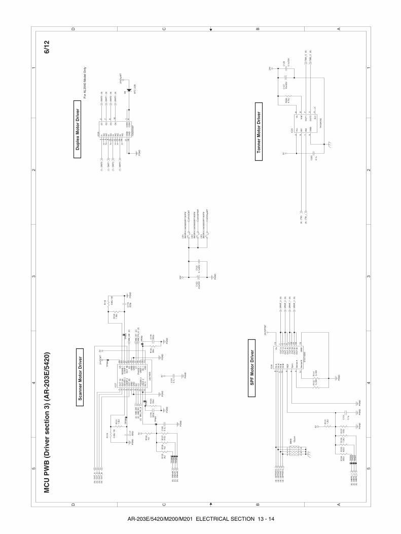
PG
ND
PG
ND
5V
24V
SP
FM
T
24V
DupM
T
PG
ND
PG
ND
24V
PG
ND
PG
ND
24V
SC
MT
PG
ND
PG
ND
PG
ND
PG
ND
24V
SC
MT
PG
ND
5V
24V
DupM
T
5V
5V
PG
ND
PG
ND
5V
PG
ND
24V
SP
FM
T
24V
OU
T_A
-(9
)
TM
B_O
(9)
(SP
FM
T1)
(4)
SP
MT
_3
(9)
MM
ref2
(5)O
UT
_B
+(9
)
(TM
)(4
)
(SP
FM
T3)
(4)
TM
A_O
(9)
MM
_B
I0(2
)
MM
_A
I0(2
)
(SP
FM
T0
)(4
)
MM
_P
H_A
(2)
MM
_A
I1(2
)
/DM
T3
(9)
OU
T_B
-(9
)
(SP
FM
T2)
(4)
(TM
_)
(4)
OU
T_A
+(9
)
SP
MT
_2
(9)
MM
ref1
(5)
DM
T1
(1)
DM
T0
(1)
/DM
T2
(9)
DM
T2
(1)
MM
ref0
(5)
MM
_P
H_B
(2)
SP
MT
_1
(9)
/DM
T1
(9)
DM
T3
(1)
/DM
T0
(9)
MM
_B
I1(2
)
MR
PS
_3
(5)
MR
PS
_2
(5)
MR
PS
_1
(5)
SP
MT
_0
(9)
Scanner Motor Driver
SPF
Motor Driver
Duplex
Motor Driver
Tonner Motor Driver
For
AL2040 M
odel O
nly
TP
597
R135
620J
TP
595
C128
0.1
u/5
0V
R120
1.5
kJ
R136
1.2
kJ
R118
0.6
8J 1
W
R137
100J
TP
596
TP
586
C222
0.1
u
C116
820p
R131
1.2
kJ
R123
30kJ
R121
1.5
kJ
C121
0.1
u
C118
82
0p
R119
0.6
8J 1
W
R122
1kJ
IC26
TD
62064A
F
I13
NC
4
NC
5
I26
NC
10
I31
1
NC
12
NC
13
GN
D1
7
O1
2
O2
7
O3
9
O4
16
CO
M1
CO
M8
GN
D1
8
I41
4
NC
15
C117
820p
R124
30kJ
BR
59
10kJx4
1234
8765
C119
820p
IC29
TA
7291A
S
Vcc
2
IN1
9
IN2
1
GN
D5
OU
T2
3
OU
T1
7
Vre
f8
Vs
6
N.C
4
+C
122
47u/3
5V
D6
MT
Z J
22B
C131
0.1
u
R127
510J
R126
1kJ
R132
1J 2
W
C120
0.1
uR
125
2kJ
C123
0.1
u/5
0V
IC28
ST
A7100MO
UT
A1
OU
T A
2
OU
T A
/3
OU
T A
/4
Vs
13
OU
T B
17
OU
T B
18
OU
T B
/1
5
OU
T B
/1
6
GN
D1
0
IN A
8
IN A
/7
IN B
11
IN B
/1
2
RE
F9
Se
nse
A5
Se
nse
B1
4
Syn
c6
TP
593
+C
127
10u/3
5V
CP
10603F
A1.5
A/0
603S
FF
150F
M
R244
4.7
kJ
TP
587
IC27
L6219D
S
OU
T 2
A2
SE
NS
E 2
3
CO
MP
24
OU
T 2
B5
GN
D6
GN
D7
I02
8
I12
9
PH
AS
E 2
10
VR
EF
21
1
RC
21
2V
SS
13
RC
11
4V
RE
F 1
15
PH
AS
E 1
16
I11
17
GN
D1
8G
ND
19
I01
20
OU
T 1
B2
1C
OM
P 1
22
SE
NS
E 1
23
VS
24
OU
T 1
A1
TP
590
R134
300J
TP
588
R141
1J 2
W
TP
591
CP
20603F
A1.5
A/0
603S
FF
150F
M
TP
589
TP
594
TP
592
CP
30603F
A1.5
A/0
603S
FF
150F
M
5 5
4 4
3 3
2 2
1 1
DD
CC
BB
AA
MC
U P
WB
(D
rive
r se
ctio
n 3
) (A
R-2
03E
/542
0)6/
12
AR-203E/5420/M200/M201 ELECTRICAL SECTION 13 - 14

VC
C3
5V
INT
5V
PG
ND
VC
C3
EN
5V
VC
C3
5V
PG
ND
12
V
5V
24
V
VC
C3
INT
24
V
INT
24
V
5V
5V
5V
5V
PG
ND
5V
VC
C3
(PD
2)
(4)
DV
SE
L(1
2)
(DR
ST
)(4
)D
RS
T(8
)
PD
2(9
)
(PP
D3
)(4
)
(CE
D1
)(4
)
(TC
S)
(4)
(MM
LD
)(4
)
PP
D1
(9)
(PP
D1
)(4
)
TC
S(1
2)
PS
W(8
)
(CE
D2
)(4
)C
ED
1(9
)
(SP
PD
)(1
)
CE
D2
(9)
PP
D3
(9)
(PP
D2
)(4
)
(PM
RD
Y)
(4)
(PO
D)
(4)
12
VIN
(8)
DV
S1
(4)
PM
RD
Y(9
)
SP
PD
(9)
MF
D(9
)(M
FD
)(4
)
PO
D(9
)
PD
1(9
)(P
D1
)(4
)
PP
D2
(9)
SP
ID(9
)
3.3
VIN
(8)
(PS
W)
(1)
MM
LD
(9)
(SP
ID)
(4)
DS
WS
(4)
24
V1
(DS
WS
)(9
)
(FA
NL
K)
(4)
FA
NL
K(9
)
R1
60
1kJ
L1
5N
.M.
R1
66
15
kJ
R1
43
0.2
2J 2
W
R3
98
10
0kJ
R1
78
12
kJ
C1
79
0.1
u
C1
53
0.1
u
R3
77
10
kJ
R1
67
10
kJ
D1
4
KD
S2
26
213
R1
79
3.3
kJ
C2
24
10
00
p
C1
71
10
00
p
R3
78
1kJ
C1
54
0.1
u
D1
5
KD
S2
26
213
R1
47
4.7
kJ
R1
75
7.5
kJ
C1
64
10
00
p
C1
72
10
00
p
D1
6
KD
S2
26
213
R1
76
7.5
kJ
C1
55
0.1
u
C1
68
0.1
u
R1
52
1kJ 2
W
C1
73
10
00
p
R3
99
10
0kJ
C1
86
10
00
p
C2
23
10
00
p
R1
72
10
0J 2
W
C1
35
0.1
u
C1
56
0.1
u
C1
89
10
00
p
C2
26
10
00
p
R1
80
1kJ
C1
90
10
00
p
D1
8
KD
S2
26
213
TP
15
1
C1
57
0.1
u
D52
ZENER_UDZS4.7B(open)
R1
81
1kJ
+C
18
1
22
u/1
6V
C1
36
N.M
.
R3
94
10
0kJ
C1
87
10
00
p
D2
01
SS
35
5
D1
9
KD
S2
26
213
D1
0
KD
S2
26
213
C1
63
10
00
p
IC3
0
KIA
78
05
IN1
GN
D
2
OU
T3
C1
83
0.1
u
R1
82
1kJ
C1
58
0.1
u
C1
88
10
00
p
D2
1
KD
S2
26
213
D1
7
KD
S2
26
213
D9
KD
S2
26
213
R2
42
10
J
C1
84
0.1
u
R1
83
1kJ
D1
3
KD
S2
26
213
D2
2
KD
S2
26
213
C1
59
N.M
.
C1
37
0.1
u
R1
49
10
kJ
R1
45
15
kJ
C1
76
0.1
u
+C
18
2
22
u/1
6V
R2
40
10
J
R1
84
1kJ
D51
ZENER_UDZS4.7B(open)
C1
46
N.M
.
R1
68
1kJ
+C
17
5
47
u/3
5V
C1
61
10
00
p
C1
80
0.1
u
R1
85
1kJ
C1
47
N.M
.
C1
38
0.1
u
R1
69
1kJ
C1
67
10
00
p
L5
ZJS
R5
10
1-2
23
R1
48
10
kJ
R1
86
1kJ
L1
40
J (
16
08
)
R1
70
1kJ
+C
17
8
22
u/1
6V
R1
77
7.5
kJ
C1
48
N.M
.
D1
2
1S
S3
55
C1
40
N.M
.
C1
39
N.M
.
R1
71
1kJ
TP
16
1
D1
11
SS
35
5
C1
49
0.1
u
C2
48
10
00
p
C1
41
N.M
.
C2
25
10
00
p
TP
58
5
C1
85
10
00
p
C1
50
0.1
u
C1
42
N.M
.
D2
7
KD
S2
26
213
R1
59
1kJ
R1
73
15
kJ
R1
54
1kJ
C1
66
10
00
p
D2
8
KD
S2
26
213
C1
43
N.M
.
D2
5
KD
S2
26
213
+C
16
9
47
u/3
5V
+C
17
7
47
u/2
5V
R3
96
10
0kJ
R2
41
10
J
D2
3
KD
S2
26
213
C1
44
N.M
.
R1
51
10
kJ
C1
70
0.1
u/5
0V
R1
56
1kJ
TP
13
1
L4
ZJS
R5
10
1-2
23
(op
en
)
D2
6
KD
S2
26
213
D5
0
KD
S2
26
213
C1
45
N.M
.
D2
9
KD
S2
26
213
R1
63
2.7
kJ
R1
57
1kJ
D2
4
KD
S2
26
213
R3
97
10
0kJ
C1
51
0.1
u
R1
64
10
kJ
R1
61
20
kJ
C1
65
10
00
p
TP
14
1
R2
43
10
J
R1
58
1kJ
R1
65
10
kJ
R1
62
20
kJ
R1
50
15
kJ
C1
52
0.1
u
R1
74
15
kJ
5 5
4 4
3 3
2 2
1 1
DD
CC
BB
AA
MC
U P
WB
(N
ois
e fi
lter
/Pu
ll-u
p s
ecti
on
) (A
R-2
03E
/542
0)7/
12
AR-203E/5420/M200/M201 ELECTRICAL SECTION 13 - 15
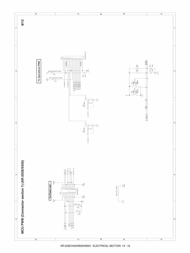
KE
YIN
2#
KE
YIN
1#
KE
YIN
2#
KE
YIN
1#
EN
5V
24
V
INT
24
V
PG
ND
5V
INT
5V
PG
ND
5V
5V
EN
5V
PG
ND
HL
OU
T(5
)/P
R(5
)
/MC
(5)
/BIA
S(5
)/T
C(5
)
12
VIN
(7)
3.3
VIN
(7)
/GR
IDL
(5)
FW
(4)
/PO
FF
(5)
PS
L(1
)
(SE
LIN
2)
(4)
KE
YIN
1(4
)
(OP
_D
AT
A)
(4)
(SE
LIN
3)
(4)
KE
YIN
2(4
)
PS
W(7
)
ON
L(1
)
(OP
_C
LK
)(4
)(S
EL
IN1
)(4
)
(OP
_L
AT
CH
)(4
)
(ST
RO
BE
)(4
)
DR
ST
(7)
To
Operational PWB
To
Power unit
R1
90
1kJ
C193
0.1u/50V
D3
1
KD
S2
26
213
R4
00
N.M
._1
60
8siz
e
C1
95
10
00
p
CN
2
IMS
A-9
61
9S
-18
A
12345678910
11
12
13
14
15
16
17
18
R1
87
10
kJ
Q5
KR
C1
06
S
1
2
3
C194
N.M._1608size
Q6
KR
C1
06
S
1
2
3
CP7
0603FA1.5A/0603SFF150FM
CN
1
B2
4B
-PN
DZ
S-1
1 3 5 7 9 11
13
15
17
19
21
23
2 4 6 81
01
21
41
61
82
02
22
4
D3
0
KD
S2
26
213
R1
88
10
kJ
C1
92
10
00
p
C1
91
10
00
p
CP8
0603FA1.5A/0603SFF150FM
R1
89
1kJ
5 5
4 4
3 3
2 2
1 1
DD
CC
BB
AA
MC
U P
WB
(C
on
nec
tor
sect
ion
1)
(AR
-203
E/5
420)
8/12
AR-203E/5420/M200/M201 ELECTRICAL SECTION 13 - 16
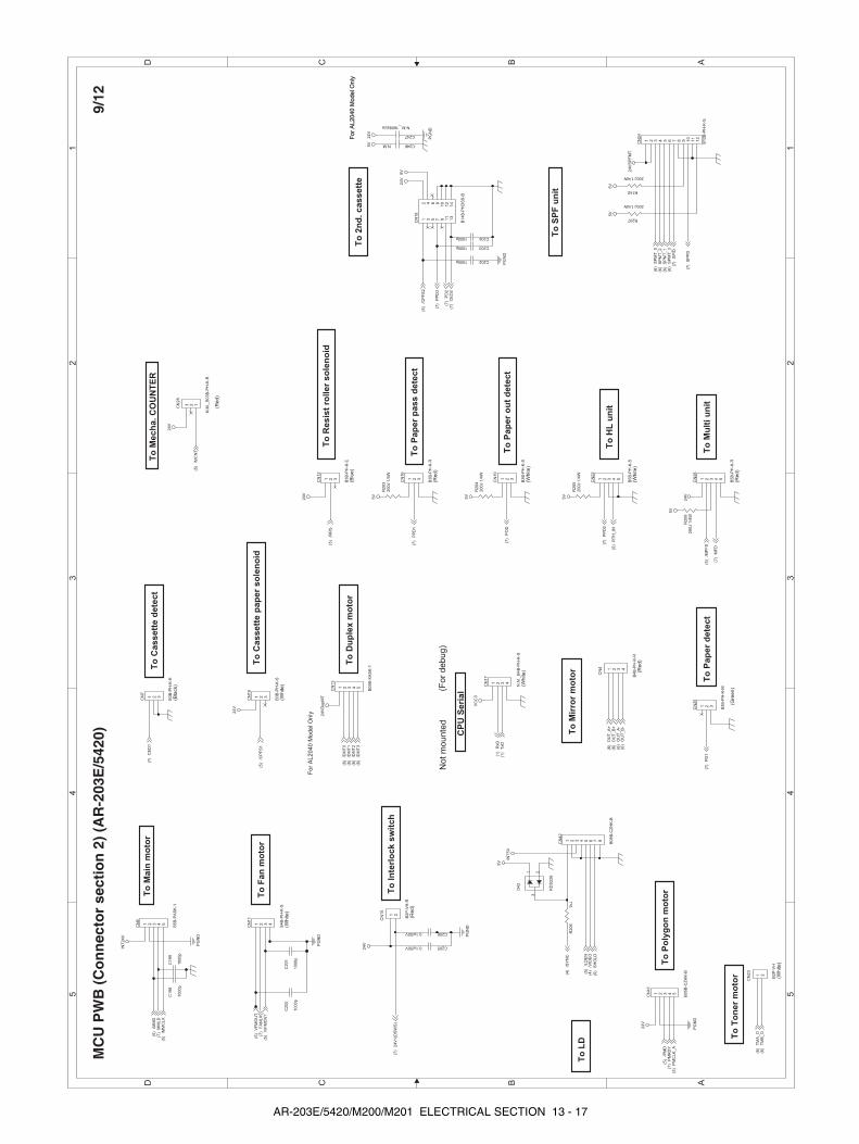
24V
PG
ND
5V
5V
24VPG
ND
5V
24V
24V
SP
FM
T
24V
5V
5V
5V
VC
C3
5V
PG
ND
24V
INT
24V
PG
ND
24V
DupM
T
24V
PG
ND
24V
5V
24V
PG
ND
INT
5V
5V
/VF
MC
NT
(5)
TM
B_O
(6)
/RR
S(5
)
PD
1(7
)
/DM
T1
(6)/C
PF
S1
(5)
24V
1(D
SW
S)
(7)
/MP
FS
(5)
SP
ID(7
)
PP
D1
(7)
VF
MO
UT
(5)
TM
A_O
(6)
PO
D(7
)
/DM
T0
(6)
SP
MT
_1
(6)
/DM
T3
(6)
PP
D2
(7) RT
H_IN
(5)
MF
D(7
)
SP
PD
(7)
CE
D1
(7)
/DM
T2
(6)
SP
MT
_3
(6)
TxD
(1)
PD
2(7
)PP
D3
(7)
CE
D2
(7)/C
PF
S2
(5)
OU
T_B
+(6
)O
UT
_A
-(6
)O
UT
_B
-(6
)
OU
T_A
+(6
)
/MM
D(5
)M
ML
D(7
) /MM
CLK
(5)
/MC
NT
(5)
FA
NLK
(7)
RxD
(1)
/PM
D(5
)
PM
CLK
_A
(5)
PM
RD
Y(7
)
/SY
NC
(4)
/LD
EN
(5)
/VID
EO
(4)
SH
OLD
(5)
SP
MT
_0
(6)
SP
MT
_2
(6)
(White)
(White)
To
SPF
unit
(Fo
r d
eb
ug
)
To
Paper detect
(Red)
CPU
Serial
(White)
(Blu
e)
To
Cassette paper solenoid
(White)
(White)
No
t m
ou
nte
d
To
Polygon
motor
To
Paper pass
detect
To
Fan
motor
To
HL
unit
(Bla
ck)
To
Cassette detect
(Red)
To
Toner motor
(Red)
To
Duplex motor
To
Interlock switch
To
Multi unit
To
Paper out detect
To
Resist roller solenoid
To
2nd. cassette
To
Mirror motor
To
Main
motor
To
Mecha. COUNTER
(Red)
(Red)
Fo
r A
L2
04
0 M
od
el O
nly
Fo
r A
L2
04
0 M
od
el O
nly
For
AL2040 M
odel O
nly
(Gre
en)
To
LD
(White)
CN
18
B14B
-PH
DS
S-B
1 3 5 7 9 11
13
2 4 6 810
12
14
CN
10
B3B
-PH
-K-S
1 2 3
R140
200J 1/4W
CN
12
B3B
-PH
-K-E
1 2 3
CN
16
B3B
-PH
-K-R
1 2 3
R208
200J 1
/4W
CN
19
B3B
-PH
-K-S
1 2 3
CN
17
N.M
._B
4B
-PH
-K-S
1 2 3 4
CN
6
B5B
-PA
SK
-1
1 2 3 4 5
CN
13
B05B
-XA
SK
-1
1 2 3 4 5
CN
7
B3B
-PH
-K-K
1 2 3
R205
200J 1
/4W
R203
200J 1
/4W
C201
1000p
R204
200J 1
/4W
C200
1000p
CN
25
B3B
-PH
-K-M
1 2 3
C199
1000p
C2050.1u/50V
C2060.1u/50V
D42
KD
S226
213
CN
24
B12B
-PH
-K-S
1 2 3 4 5 6 7 8 9 10
11
12
C198
1000p
C2021000p
CN
11
B4B
-PH
-K-S
1 2 3 4
C2031000p
CN
15
B2P
-VH
-R
1 2
C2041000p
CN
28
N.M
._B
03B
-PH
-K-R
123
C246N.M.
CN
23
B2P
-VH
1 2
R207
200J 1/4W
CN
22
B5B
-PH
-K-S
1 2 3 4 5
CN
41
B05B
-CZ
HK
-B
1 2 3 4 5
C247
N.M._1608size
CN
26
B5B
-PH
-K-R
1 2 3 4 5
R206
1kJ
CN
4
B4B
-PH
-K-R
1 2 3 4
CN
42
B08B
-CZ
HK
-B
1 2 3 4 5 6 7 8
5 5
4 4
3 3
2 2
1 1
DD
CC
BB
AA
MC
U P
WB
(C
on
nec
tor
sect
ion
2)
(AR
-203
E/5
420)
9/12
AR-203E/5420/M200/M201 ELECTRICAL SECTION 13 - 17

AF
E_
DB
#0
AF
E_
DB
#6
AF
E_
DB
#6
VC
L
AF
E_
DB
#4
AF
E_
DB
#0
AF
E_
DB
#7
AF
E_
DB
#3
VC
L
AF
E_
DB
#7
AF
E_
DB
#5
AF
E_
DB
#1
VC
L
AF
E_
DB
#4
AF
E_
DB
#2
AF
E_
DB
#5
AF
E_
DB
#3
AF
E_
DB
#2
AF
E_
DB
#1
PG
ND
PG
ND
VC
C3
PG
ND
24
V
12
VE
N5
V
CL
(2)
AF
E_
SD
I#(4
)C
CD
_C
P#
(4)C
CD
_P
HI1
#(4
)
VS
AM
P#
(4)
BS
AM
P#
(4)
AD
CL
K#
(4)
mt_
at_
ho
me
(4)
AF
E_
SE
N#
(4)
CC
D_
TG
#(4
)C
CD
_R
S#
(4)C
CD
_P
HI2
#(4
)
AF
E_
SC
K#
(4) AF
E_
DB
#[7
..0
](4
)
To
Scanner unit
Copy Lamp
Inverter
R2
09
91
0J
C2
09
0.1
u/5
0V
R2
13
1kJ
CN
3
FF
4-3
2-S
15
D5
135791
11
31
51
71
92
12
32
52
72
93
1
246810
12
14
16
18
20
22
24
26
28
30
32
R212
5.6kJ 1/4W
CP
9
06
03
FA
1.5
A/0
60
3S
FF
15
0F
M
+C
20
8
47
u/3
5V
D4
41
1E
QS
06
L6
22
0u
H
TW
KA
-22
1K
Q9
2S
J5
37
R2
14
15
kJ
R2
15
56
kJ
C2
10
33
p
Q8
KT
C3
19
8
R2
10
15
kJ
CP
60
60
3F
A1
.5A
/06
03
SF
F1
50
FM
R2
11
12
kJ
C2
11
10
00
p
D4
3
KD
S2
26
213
CP
10
06
03
FA
1.5
A/0
60
3S
FF
15
0F
M
+C
20
74
7u
/35
V
5 5
4 4
3 3
2 2
1 1
DD
CC
BB
AA
MC
U P
WB
(S
can
ner
I/F
sec
tio
n)
(AR
-203
E/5
420)
10/1
2
AR-203E/5420/M200/M201 ELECTRICAL SECTION 13 - 18
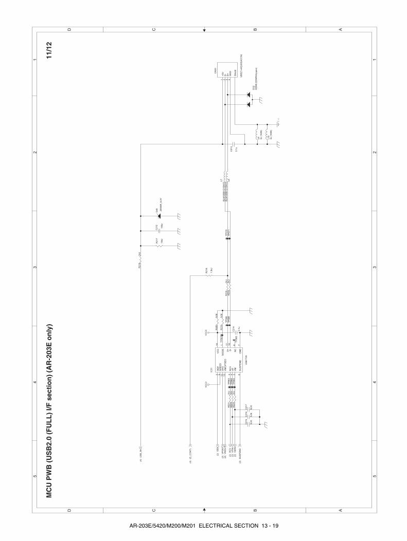
VC
C3
VC
C3
VP
OU
T(2
)V
MO
UT
(2)
US
B_
IN(4
)
OE
N(2
)
VP
IN(2
)V
MIN
(2)
RC
V(2
)
SU
SP
EN
D(2
)
(D_
CO
NT
)(4
)
F.G
C2
17
N.M
.
L7
BL
M1
8B
B1
21
SN
1D
TP
56
7
IC3
1
US
B1
T2
0MO
DE
1
OE
#2
RC
V3
VP
4
VM
5
SU
SP
EN
D6
GN
D7
NC
8
SP
EE
D9
D-
10
D+
11
VP
O12
VM
O/F
SE
O13
VC
C14
D3
2H
ZM
6.2
Z4
MW
A(o
pe
n)
TP
56
8
C2
15
N.M
.
C2
12
10
0p
TP
56
9
R2
17
10
kJ
R4
20
N.M
.
TP
57
0
D4
5
ZE
NE
R_
6.2
V
TP
57
1
L9
0J (
16
08
)
L8
BL
M1
8B
B1
21
SN
1D
R2
20
24
J
R2
16
24
J
TP
56
3
CN
33
UB
S2
1-4
K2
J0
0(A
CO
N)
+5V
1
D-
2
D+
3
GN
D4
Shie
ld
L1
60
J (
16
08
)
C2
13
0.1
u
R2
18
1.5
kJ
TP
56
4R
22
13
3J
R2
22
24
J
TP
56
5R
22
33
3J
C2
16
N.M
.
C2
14
0.1
u
TP
56
6
R2
19
N.M
.
R2
24
33
J
5 5
4 4
3 3
2 2
1 1
DD
CC
BB
AA
MC
U P
WB
(U
SB
2.0
(FU
LL
) I/F
sec
tio
n)
(AR
-203
E o
nly
)11
/12
AR-203E/5420/M200/M201 ELECTRICAL SECTION 13 - 19
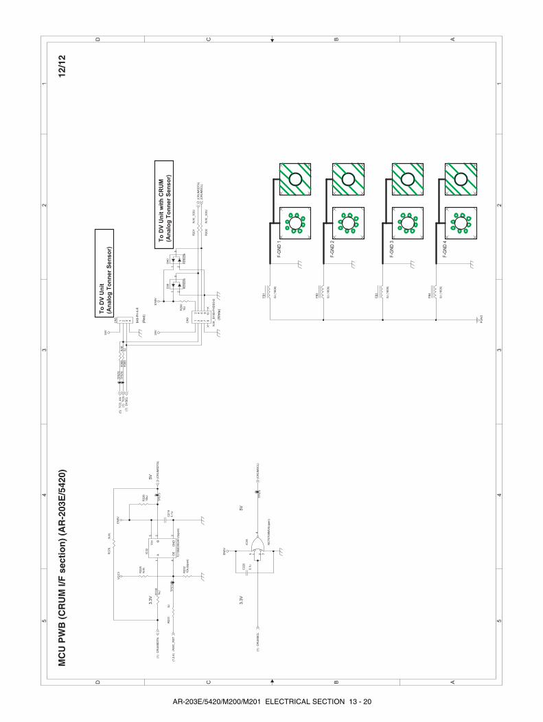
EN
5V
EN
5V
VC
C3
24
VE
N5
V
24
V
PG
ND
/AS
IC_
RS
T(1
,2,4
)
(CR
UM
SC
L)
CR
UM
SC
L(1
)
(CR
UM
SD
TA
)C
RU
MS
DT
A(1
)
(CR
UM
SC
L)
TC
S(7
) DV
SE
L(7
)
(CR
UM
SD
TA
)
TC
S_
AN
(5)
5V
5V
3.3
V
3.3
V
(White)
To
DV
Unit
with
CRUM
(Analog
Tonner Sensor)
(Red)
To
DV
Unit
(Analog
Tonner Sensor)
F-G
ND
3
F-G
ND
4
F-G
ND
2
F-G
ND
1
D4
0
KD
S2
26
213
TP
57
2
R2
02
N.M
._3
00
J
IC3
4
NC
7S
T0
8M
5X
(op
en
)
1 2 3
4
5
R2
01
N.M
._3
00
J
C2
20
0.1
u
R1
39
1kJ
CN
5
B4
B-P
H-K
-R
1 2 3 4
FB
1
0J (
16
08
)
TP
57
6
TP
57
3
R2
26
10
kJ
FB
3
0J (
16
08
)
R2
25
N.M
.
TP
57
4
R2
31
0J
TP
57
5
R3
69
0J
C2
18
0.1
u
FB
2
0J (
16
08
)
FB
4
0J (
16
08
)
R2
32
10
kJ(o
pe
n)
R2
00
10
J
IC3
2
TC
7S
BD
38
5A
FU
(op
en
)
A1
B2
OE
4G
ND
3
Vcc
5
R3
76
N.M
.
D3
9
KD
S2
26
213
R3
68
N.M
.
N.M
._B
10
B-P
HD
SS
-B
CN
9
1 3 5 7 9
2 4 6 81
0
5 5
4 4
3 3
2 2
1 1
DD
CC
BB
AA
MC
U P
WB
(C
RU
M I/
F s
ecti
on
) (A
R-2
03E
/542
0)12
/12
AR-203E/5420/M200/M201 ELECTRICAL SECTION 13 - 20
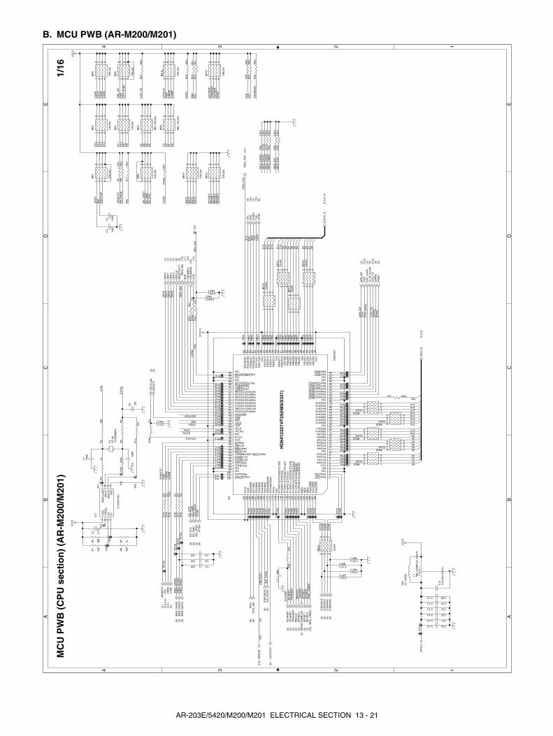
B. MCU PWB (AR-M200/M201)A A
B B
C C
D D
E E
44
33
22
11
CP
UC
LK
(FW
)
/LW
R#
/CS
0#
/CS
2#
CP
U_
SY
NC
/CS
1#
SC
L
CC
D_
TG
SD
A
AR
B_
INT
A0
A5
A2
A4
A11
A19
A13
A3
A8
A10
A7
A12
A16
A14
A18
A1
A15
A17
A6
A9
/HW
R#
/RD
#
(SP
PD
)
CP
U_
SY
NC
/RE
S_
NIC
(PS
W)
CC
D_
TG
(FW
)A
RB
_IN
T
/CS
3#
/RE
S_
US
B2
0PR
OT
EC
T
DM
T3
/WD
TO
VF
D1
4
P60
PO
FF
D8
D5
D1
DM
T0
D1
D1
5
D7
D1
1
D3
D0
D1
2
D1
1
D1
3
D8
D3
P6
0
D1
0
D4
D7
D5
DM
T1
D9
DM
T2
D6
D2
D9
D1
4
D6
D4
D1
0
/STBY
/ST
BY
/PR
INT
ST
D1
2
D1
5
D2
D1
3
/ES
_S
RD
YE
S_
CM
DE
S_
ST
S
ES
_C
MD
/ES
_S
RD
Y
/PR
INT
ST
ES
_S
TS
/RD
#
/LW
R#
/HW
R#
DM
T3
DM
T0
DM
T2
DM
T1
NM
I
NMI
/WDTOVF
RS
V_
IN0
EX
TA
L
XT
AL
SP
FM
T1
SP
FM
T3
SP
FM
T2
SP
FM
T0
/ES
_P
AG
E
D0
RY
/BY
RxD
SP
FM
T0
SP
FM
T1
SP
FM
T2
/TR
AN
SS
T
SP
FM
T3
/SC
AN
ST
/ES
_P
AG
E
/SC
AN
SP
RY
/BY
/CS
5#
/CS
5#
/SC
AN
ST
/SC
AN
SP
/TR
AN
SS
T
/RE
S_
FA
X/R
ES
_N
IC
/RE
S_
US
B2
0
/RE
S_
OA
98
2
/RE
S_
IOA
SIC
/RE
S_
GA
SIC
/RE
S_
GA
SIC
/RE
S_
IOA
SIC
/RE
S_
OA
98
2
/CS
3#
/CS
1#
/CS
0#
/CS
2#
A20
CPUCLK
EXTALXTAL
/RE
S_
FA
XS
CL
RxD
SD
AT
XD
PO
FF
CR
UM
SD
A
TxD
CP
U3
.3
CP
U3
.3
VC
C3
VC
C3
VC
C3
A[2
0..
0]
(2,3
,4)
(PS
W)
(8)
CC
D_
TG
(2,5
)
/PR
INT
ST
(2)
CP
U_
SY
NC
(2)
AR
B_
INT
(2)
D[1
5..
0]
(2,3
,4,1
3)
(SP
PD
)(8
)
(FW
)(5
,9)
DM
T2
(7)
DM
T1
(7)
DM
T0
(7)
DM
T3
(7)
(TC
S_
AN
)(6
)R
TH
(6)
ES
_S
TS
(9)
ES
_C
MD
(9)
/HW
R(3
,4)
/LW
R(2
)
/ES
_S
RD
Y(9
)
/CS
IOA
SIC
(3)
/CS
GA
SIC
(2)
/CS
SR
AM
(4)
/CS
FR
OM
(4)
SD
A(4
)
MM
CL
K(6
)
/RD
(2,3
,4,5
)
PO
FF
(6)
TxD
(12
)
RxD
(12
)S
CL
(4)
BZ
R(1
1)
/ES
_P
AG
E(9
)
CR
UM
SD
A(1
6)
CR
UM
SC
L(1
6)
SP
FM
T3
(5)
SP
FM
T0
(5)
SP
FM
T1
(5)
/SC
AN
SP
(2)
PM
CL
K(6
)
SP
FM
T2
/MIR
CN
T(5
)
/TR
AN
SS
T(2
)/S
CA
NS
T(2
)
RY
/BY
(4)
/CS
5(1
3)
CP
UC
LK
#(3
)/R
ES
ET
1(5
)
VID
EO
#(2
,5)
LC
DC
ON
T(6
)
RE
SE
TO
UT
1(5
)
mt_
at_
ho
me
#(5
)
/RE
S_
US
B2
0(1
0)
/RE
S_
FA
X(1
3)
/RE
S_
OA
98
2(9
)
/RE
S_
GA
SIC
(2)
/RE
S_
IOA
SIC
(3)
/RE
S_
NIC
(15
)
(PS
FA
NL
K)
(8)
TP9
TP
65
TP35
TP86
C200.1U
C250.1UB
R7
NM
_1
0K
JX
4
1 2 3 4
8 7 6 5
FB
10
J<
16
08
>
R1
32
10
KJ
R2
61
0K
J
R3
64
33
J
TP
52
TP
66
TP22
R9
41
0K
J
R5
13
3J
TP
79
BR2133JX4
1234
8765
TP101
BR
9
NM
_1
0K
JX
4
1 2 3 4
8 7 6 5
TP32
TP81
R4
NM
TP
72
R2
32
KJ
TP106
BR2233JX4
1234
8765
TP
44
R5033J
BR
3
10
KJX
4
1 2 3 4
8 7 6 5
TP95
IC2
H8
S/2
32
1
HD
6412
321V
F25
(H8S
/232
1)
P35/S
CK
164
P34/S
CK
063
P33/R
xD
162
P32/R
xD
061
P31/T
xD
160
P30/T
xD
059
VC
C58
PD
7/D
15
57
PD
6/D
14
56
PD
5/D
13
55
PD
4/D
12
54
Vss
53
PD
3/D
11
52
PD
2/D
10
51
PD
1/D
950
PD
0/D
849
PE
7/D
748
PE
6/D
647
PE
5/D
546
PE
4/D
445
Vss
44
PE
3/D
343
PE
2/D
242
PE
1/D
141
PE
0/D
040
VC
C39
AV
cc
10
3
Vre
f1
04
P40/A
N0
10
5
P41/A
N1
10
6
P42/A
N2
10
7
P43/A
N3
10
8
P44/A
N4
10
9
P45/A
N5
11
0
P46/A
N6/D
A0
11
1
P47/A
N7/D
A1
11
2
AV
ss
11
3
Vss
11
4
P17/P
O15/T
IOC
B2/T
CLK
D1
15
P16/P
O14/T
IOC
A2
11
6
P15/P
O13/T
IOC
B1/T
CLK
C1
17
P14/P
O12/T
IOC
A1
11
8
P13/P
O11/T
IOC
D0/T
CLK
B1
19
P12/P
O10/T
IOC
C0/T
CLK
A1
20
P11/P
O9/T
IOC
B0/D
AC
K1
12
1
P10/P
O8/T
IOC
A0/D
AC
K0
12
2
MD
01
23
MD
11
24
MD
21
25
PG
0/C
AS
12
6
PG
1/C
S3
12
7
PG
2/C
S2
12
8
PG3/CS11
PG4/CS02
Vss3
NC4
VCC5
PC0/A06
PC1/A17
PC2/A28
PC3/A39
Vss10
PC4/A411
PC5/A512
PC6/A613
PC7/A714
PB0/A815
PB1/A916
PB2/A1017
PB3/A1118
Vss19
PB4/A1220
PB5/A1321
PB6/A1422
PB7/A1523
PA0/A1624
PA1/A1725
PA2/A1826
PA3/A1927
Vss28
PA4/A20/IRQ429
PA5/A21/IRQ530
PA6/A22/IRQ631
PA7/A23/IRQ732
P67/CS7/IRQ333
P66/CS6/IRQ234
Vss35
Vss36
P65/IRQ137
P64/IRQ038
P53/ADTRG102
P52/SCK2101
Vss100
Vss99
P51/RxD298
P50/TxD297
PF0/BREQ96
PF1/BACK95
PF2/LCAS/WAIT/BREQO94
PF3/LWR93
PF4/HWR92
PF5/RD91
PF6/AS90
VCC89
PF7/088
Vss87
EXTAL86
XTAL85
VCC84
STBY83
NMI82
RES81
WDTOVF80
P20/PO0/TIOCA379
P21/PO1/YICOB378
P22/PO2/TIOCC377
P23/PO3/TIOCD376
P24/PO4/TIOCA475
P25/PO5/TIOCB474
P26/PO6/TIOCA573
P27/PO7/TIOCB572
P63/TEND171
P62/DREQ170
P61/TEND0/CS569
Vss68
Vss67
P60/DREQ0/CS466
Vss65
TP13T
P5
9
TP
40
TP24
TP
43
TP
2
TP
48
TP15
BR2333JX4
1234
8765
TP
70
BR
5
10
KJX
4
1 2 3 4
8 7 6 5
TP26
TP10
TP98
TP93
TP84
C2
0.1
U
TP
73
4
C70NM
BR2433JX4
1234
8765
TP
72
4
TP17
C4
10
0P
R5
21
0K
J
TP
67
TP28
TP
76
TP
51
TP102
TP87
R1
91
0K
J
C833P
TP
80
BR2533JX4
1234
8765
R1
22
2J
R1
63
3J
TP
6
R6
61
0K
J
BR
10
10
KJX
4
1234
8765
TP
54
TP
56
TP19
R2
NM
TP107
TP90
C1222P
R1
110K
J
BR
16
33
JX
41 2 3 4
8 7 6 5
C14NM
TP
73
BR
6
10
KJX
4
1 2 3 4
8 7 6 5
C13NM
C6
12
P
C15NM
BR
17
33
JX
41 2 3 4
8 7 6 5
R1
73
3J
TP96
BR
13
10
KJX
4
1 2 3 4
8 7 6 5
R2
03
30
J
TP
61
TP11
R9
10
KJ
C933P
R1
NM
TP
73
5
TP
64
X1
AT
-49
19
.66
08
MH
z
BR
18
33
JX
41 2 3 4
8 7 6 5
R6
71
0K
J
TP37
TP29
TP
5
TP103
TP99
TP85
TP
78
TP36
C210.1U
BR
19
33
JX
41 2 3 4
8 7 6 5
R1
83
3J
R3
84
33
J
TP
69
TP
38
TP20
C220.1U
TP108
R3
0J
TP
47
TP88
BR
20
33
JX
4
1234
8765
R1
33
3J
R6
NM
C230.1U
C733P
TP
7
TP
55
TP23
BR
12
10
KJX
4
1 2 3 4
8 7 6 5
TP33
TP
3
C10NM
TP
10
9
TP
68
C240.1U
R5
10
KJ
TP12
TP91
TP82
R7
81
KJ
TP
42
TP
75
TP
46
TP14
TP
1
TP25
R7
0J
TP
72
9
R8
NM
C1
91
0U
/10
V<
20
12
>
TP30
C3
10
0P
C5
15
PF
TP
63
TP16
TP97
BR
1
10
KJX
4
1 2 3 4
8 7 6 5
TP
49
TP27
R2
23
3J
R3
92
10
KJ
R2
12
KJ
TP
74
R9
51
0K
JT
P5
0
TP8
BR
11
10
KJX
4
1 2 3 4
8 7 6 5
TP100
C369NM
TP
53
TP34
TP
71
R1
51
00
J
L1
NM
_Z
JS
R5
10
1-2
23
TA
TP
4
TP21
TP94
TP89
R2
53
3J
TP
57
R2
41
0K
J
TP31
BR
2
10
KJX
4
1 2 3 4
8 7 6 5
IC1
CY
25
81
1S
C
XIN
/CLK
IN1
XO
UT
8V
DD
7
VS
S2
SS
CLK
5F
RS
EL
6
S0
4
S1
3
R1
31
10
KJ
TP92
TP83
C1
15
PF
TP
77
TP105
R1
43
3J
R5
31
0K
J
TP
62
BR
4
10
KJX
4
1 2 3 4
8 7 6 5
TP
41
C1
1N
M
MC
UP
WB
(CP
Use
ctio
n)
(AR
-M20
0/M
201)
1/16
AR-203E/5420/M200/M201 ELECTRICAL SECTION 13 - 21
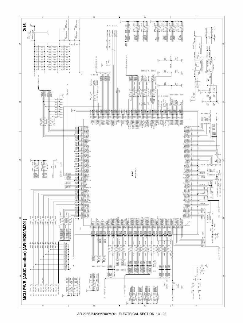
MM
_B
I2M
M_
AI0
MM
_B
I1
MM
_A
I2
MM
_B
I0
MM
_A
I1
/IN
IT/S
LC
TIN
/AU
TO
FD
/ST
B
PA
RA
D7
PA
RA
D6
PA
RA
D5
PA
RA
D4
PA
RA
D3
PA
RA
D2
PA
RA
D1
PA
RA
D0
VP
INR
CV
VM
IN
/PO
RE
Q/P
IRE
Q
PO
DA
TA
0P
OD
AT
A1
PO
DA
TA
2P
OD
AT
A3
PO
DA
TA
4P
OD
AT
A5
PO
DA
TA
6P
OD
AT
A7
CL
KS
WM
EM
_IN
T
/IN
RE
Q/O
UT
AC
K/F
AX
PR
O/P
CL
PR
O
/OU
TC
S
A8
D9
D7
RAM_CLK_OUT
D4
D2
MEM_INT
MM
_A
I0
D8
PFCLKIN
D15
PFCLKOUT
D3
D0
A7A6
A5
CLKSW
MM
_B
I1M
M_
BI0
MM
_A
I1
D1
D13
D5
D12D11
PF
CL
K
A4
A2A1
A9
A3
D6
SFCLK48
D10
PFCLK
SYNC#
D14
AF
E_
DB
7A
FE
_D
B6
AF
E_
DB
5A
FE
_D
B4
AF
E_
DB
3A
FE
_D
B2
AF
E_
DB
1A
FE
_D
B0
AF
E_
SD
I
JT
G_
TD
IJT
G_
TM
SJT
G_
TC
K
JT
G_
TD
O
MA
D1
1
MA
D8
MA
D4
MA
D1
MA
D2
MA
D5
MA
D6
MA
D9
MA
D3
MA
D0
MA
D7
MA
D1
2
MA
D1
0
AF
E_
SD
I
RA
MD
B1
5
RA
MD
B9
RA
MD
B5
RA
MD
B0
RA
MD
B3
RA
MD
B1
2
RA
MD
B1
2
RA
MD
B7
RA
MD
B6
RA
MD
B1
RA
MD
B8
RA
MD
B4
RA
MD
B2
RA
MD
B1
3
RA
MD
B9
RA
MD
B6
RA
MD
B8
RA
MD
B2
RA
MD
B1
RA
MD
B1
4
RA
MD
B7
RA
MD
B1
0
RA
MD
B5
RA
MD
B0
RA
MD
B1
1
RA
MD
B1
5
RA
MD
B1
0
RA
MD
B4
RA
MD
B1
1
RA
MD
B1
3R
AM
DB
14
/ESPRD
PO
DA
TA
0
RA
M_
CL
K_
OU
T
SY
NC
#
/SL
CT
IN/I
NIT
PE
/FA
UL
T
PA
RA
D0
PA
RA
D1
PA
RA
D2
PA
RA
D3
PA
RA
D4
PA
RA
D5
PA
RA
D6
PA
RA
D7
PID
AT
A5
PID
AT
A7
PID
AT
A0
PID
AT
A1
PID
AT
A3
PID
AT
A4
PID
AT
A6
PID
AT
A2
MM
_B
I2
MM
_A
I2
PO
DA
TA
1P
OD
AT
A2
PO
DA
TA
3P
OD
AT
A4
PO
DA
TA
5P
OD
AT
A6
PO
DA
TA
7
RC
VV
PIN
VM
IN
/RE
V
/AC
KB
US
Y
SL
CT
/AU
TO
FD
/ST
B
RS
V_
OU
T0
RS
V_
OU
T1
RS
V_
OU
T2
PF
CL
KO
UT
PF
CL
KIN
/PCLPRO/FAXPRO
/OUTACK/OUTCS/INREQ
JTG_TCKJTG_TMS
JTG_TDIJTG_TDO
AF
E_
DB
0A
FE
_D
B1
AF
E_
DB
2A
FE
_D
B3
AF
E_
DB
4A
FE
_D
B5
AF
E_
DB
6A
FE
_D
B7
RA
MD
B3
SF
CL
K4
8B
SF
CL
K4
8A
SF
CL
K4
8
SF
CL
K4
8B
S1
SF
CL
K4
8A
S0
S1
G3
.3V
VC
C3
VC
C3
VC
C3
VC
C3
G3
.3V
VC
C3
VC
C3
VC
C3
VC
C3
VC
C3
VC
C3
VC
C3
VC
C3
VC
C3
VC
C3
AF
E_
SE
N(5
)
AD
CL
K(5
)
CC
D_
CP
(5)
CC
D_
PH
I1(5
)
CC
D_
PH
I2(5
)
CC
D_
TG
(1,5
)
CL
(14
)
CC
D_
RS
(5)
VS
AM
P(5
)
AF
E_
SC
K(5
)
BS
AM
P(5
)
/H_
SY
NC
(9)
PID
AT
A[7
..0
](9
)
PO
DA
TA
[7..
0]
(9)
/PO
AC
K(9
)/P
IRE
Q(9
)
/PO
RE
Q(9
)
/PIA
CK
(9)
/PIW
R(9
)
/SC
AN
SP
(1)
/SC
AN
ST
(1)
/TR
AN
SS
T(1
)
/PR
INT
ST
(1)
OP
_C
LK
(5)
TM
(5)
TM
_(5
)
OP
_L
AT
CH
(5)
OP
_D
AT
A(5
)
MM
_Y
1(6
)
MM
_P
H_
A(7
)M
M_
AI0
(7)
MM
_A
I1(7
)
MM
_P
H_
B(7
)M
M_
BI0
(7)
MM
_B
I1(7
)
MM
_Y
2(6
)M
M_
Y3
(6) B
AN
K1
(4)
BA
NK
0(4
)
/SD
CA
S(4
)/S
DR
AS
(4)
/SD
CS
(4)
DQ
M0
(4)
MA
D[1
2..
0]
(4)
/SD
WD
E(4
)
SD
CK
E(4
)D
QM
1(4
)
CP
FS
2(6
)P
R(6
)H
L(6
)
MP
FS
(6)
MIR
ON
(5)
SP
FO
N(5
)K
EY
SC
1(5
)
KE
YS
C3
(5)
KE
YS
C2
(5)
(/A
SIC
_R
ST
)(3
,5)
/PR
_L
INE
(9)
/SC
_L
INE
(9)
/IM
C_
RE
AD
Y(9
)
RA
MD
B[1
5..
0]
(4)
A[2
0..0
](1
,3,4
)D
[15
..0
](1
,3,4
,13
)
SD
CL
K(4
)
(/S
YN
C)
(5)
/RE
V_
O(1
5)
/FA
UL
T_
O(1
5)
/AC
K_
O(1
5)
BU
SY
_O
(15
)P
E_
O(1
5)
SL
CT
_O
(15
)
PA
RA
D[7
..0
](1
5)
/RE
S_
GA
SIC
(1)
GA
SIC
_R
EA
DY
(12
)
AF
E_
DB
[7..
0]
(14
)
AF
E_
SD
I(5
)
/RE
SE
T0
(4,5
,9,1
2)
MIR
CN
T(5
)C
PU
_S
YN
C(1
)A
RB
_IN
T(1
)/C
SG
AS
IC(1
)/L
WR
(1)
/RD
(1,3
,4,5
)
VID
EO
#(1
,5)
/LE
ND
(6)
MM
D(6
)P
MD
(6)
TC
(6)
GR
IDL
(6)
MC
(6)
BIA
S(6
)V
FM
CN
T_
12
V(6
)V
FM
_2
4V
(6)
/FP
OF
F(9
)
CP
FS
1(6
)M
RP
S3
(6)
MR
PS
2(6
)M
RP
S1
(6)
LD
EN
(6)
RR
S(6
)P
TP
UL
SE
(6)
/IN
IT_
I(1
5)
/ST
B_
I(1
5)
/AU
TO
FD
_I
(15
)/S
LC
TIN
_I
(15
)
FW
RE
N(5
)
TP
87
5
TP
26
0
C340.1U
TP
87
9
TP
83
5
TP
15
7
TP
86
5
TP
84
5
TP
23
6
R6
11
0K
J
TP
22
6
TP
17
3
TP
16
0
C280.1U
TP
81
9
C350.1U
TP
19
5
R4
13
3J
R3
56
10
KJ
C7
4N
MR5
93
3J
TP
25
0
C3
71
0U
/10
V<
20
12
>
TP
82
1
C29212P
R6
9
10
J
TP124
TP113
C360.1U
TP
81
7
TP
20
4
IC4
HG
73
C1
41
HF
V(L
F)
AS
IC
CPU_DATA71
CPU_DATA62
CPU_DATA53
CPU_DATA44
CPU_DATA18
CPU_DATA36
CPU_DATA27
VCC(AC)5
CPU_DATA09
GND(AC)10
MIRCNT11
/CPUSYNC12
MEM_INT13
ARB_INT14
VCC(CORE)15
CPU_AD816
CPU_AD717
CPU_AD618
CPU_AD519
GND(CORE)20
RAM_CLK_IN21
CPU_AD422
CPU_AD323
CPU_AD224
CPU_AD125
CPU_AD026
/CPUCS27
SFCLK4828
GND(CORE)29
/CPUWR30
/CPURD31
/RESET32
PFCLK34
CLKSW35
GND(CORE)36
PFCLKOUT37
PFCLKIN38
GND(PLL)39
VCC(PLL)40
GND(PLL)41
VCC(PLL)42
TM2_15M43
/SYNC44
GND(AC)45
/VIDEO46
/LEND47
VCC(AC)48
OUTP00A49
OUTP02A51
OUTP03A52
OUTP04A53
OUTP05A54
OUTP06A55
VCC(CORE)57
OUTP15A56
OUTP07A58
OUTP08A59
GND(CORE)60
OUTP09A61
OUTP10A62
OUTP11A63
OUTP12A64
VC
C(C
OR
E)
86
OU
TP
13
B8
4
OU
TP
12
B8
3
OU
TP
10
B8
1
GND(AC)69
OU
TP
09
B8
0
OU
TP
08
B7
9
OUTP03B72
GN
D(C
OR
E)
78
OU
TP
07
B7
7
OU
TP
06
B7
6
OUTP00B68
OUTP14A67
VCC(CORE)66
OUTP13A65
VCC(AC)74
OUTP04B73
OU
TP
11
B8
2
OUTP02B71
OU
TP
05
B7
5
OU
TP
14
B8
5
OUTP01B70
TS
P_M
OD
E9
6
OP
E_
CL
K9
2
/TM
87
TM
88
OP
E_
DA
TA
89
OP
E_
LA
TC
H9
0G
ND
(AC
)9
1
VC
C(A
C)
93
/SC
AN
SP
94
TS
O0
95
IE1
28
4_
ST
B9
7IE
12
84
_A
UT
OF
D9
8V
CC
(CO
RE
)9
9IE
12
84
_S
LC
TIN
10
0IE
12
84
_IN
IT1
01
IE1
28
4_
SL
CT
10
2G
ND
(CO
RE
)1
03
IE1
28
4_
PE
10
4IE
12
84
_B
US
Y1
05
IE1
28
4_
AC
K1
06
IE1
28
4_
FA
UL
T1
07
VC
C(C
OR
E)
10
8IE
12
84
_R
EV
10
9IE
12
84
_P
AR
AD
71
10
IE1
28
4_
PA
RA
D6
11
1IE
12
84
_P
AR
AD
51
12
IE1
28
4_
PA
RA
D4
11
3IE
12
84
_P
AR
AD
31
14
IE1
28
4_
PA
RA
D2
11
5V
CC
(AC
)1
16
IE1
28
4_
PA
RA
D1
11
7IE
12
84
_P
AR
AD
01
18
SU
SP
EN
D1
19
GN
D(A
C)
12
0O
EN
12
1V
MO
UT
12
2V
PO
UT
12
3G
ND
(CO
RE
)1
24
VM
IN1
25
VP
IN1
26
RC
V1
27
/SC
AN
ST
12
8
VCC(CORE)192
/INREQ191
/OUTCS190
/OUTACK189
/ESPRD188
/FAXPRD187
/PCLPRD186
GND(AC)185
MDAT15184
MDAT14183
MDAT13182
VCC(CORE)181
MDAT12180
MDAT11179
MDAT10178
VCC(AC)177
MDAT09176
MDAT08175
MDAT07174
GND(CORE)173
MDAT06172
MDAT05171
MDAT04170
VCC(CORE)169
MDAT03168
MDAT02167
MDAT01166
MDAT00165
GND(AC)164
/INCS163
/INACK162
/OUTREQ161
GND(CORE)160
/HSYNC159
PIDATA0158
PIDATA1157
PIDATA2156
VCC(AC)155
PIDATA3154
PIDATA4153
PIDATA5152
PIDATA6151
PIDATA7150
/POCS149
/PO
RE
Q1
48
VC
C(A
C)
14
7
/PIW
T1
46
/PIA
CK
14
5
GN
D(A
C)
14
4
/PO
AC
K1
43
/PIR
EQ
14
2
GN
D(C
OR
E)
14
1
PO
DA
TA
01
40
PO
DA
TA
11
39
PO
DA
TA
21
38
PO
DA
TA
31
37
PO
DA
TA
41
36
PO
DA
TA
51
35
PO
DA
TA
61
34
PO
DA
TA
71
33
VC
C(C
OR
E)
13
2
/TR
AN
SS
T1
31
/RE
CE
PT
ST
13
0
/PR
INT
ST
12
9
RA
M_
DA
TA
42
56
RA
M_
DA
TA
52
55
RA
M_
DA
TA
62
54
RA
M_
DA
TA
72
53
GN
D(A
C)
25
2R
AM
_D
QM
02
51
RA
M_
WD
E2
50
VC
C(A
C)
24
9R
AM
_C
AS
24
8R
AM
_R
AS
24
7R
AM
_C
S2
46
RA
M_
BA
NK
S0
24
5R
AM
_B
AN
KS
12
44
VC
C(C
OR
E)
24
3R
AM
_M
AD
10
24
2R
AM
_M
AD
02
41
RA
M_
MA
D1
24
0G
ND
(CO
RE
)2
39
RA
M_
MA
D2
23
8R
AM
_M
AD
32
37
GN
D(A
C)
23
6M
M_
AI2
23
5M
M_
AI1
23
4M
M_
AI0
23
3M
M_
PH
_A
23
2
AFE_DB3217
MM
_B
I22
31
MM
_B
I12
30
MM
_Y
22
25
VCC(AC)221
MM
_Y
12
26
AFE_DB0220
AFE_DB1219
GN
D(C
OR
E)
22
3
AFE_DB2218
AFE_DB4216
AFE_DB5215
MM
_B
I02
29
MM
_P
H_
B2
28
VC
C(C
OR
E)
22
7
MM
_Y
32
24
CLPWM222
AFE_DB6214
AFE_DB7213
GND(AC)212
AFESCK211
VCC(CORE)210
ADCLK209
GND(CORE)208
AFE_SEN207
CCD_PH1206
CCD_PH2205
AFE_SDI204
CCD_CP203
BSAMP202
CCD_RS201
CCD_TG200
VSAMP199
GND(CORE)198
TD0197
TRSK195
TDI196
TCK193
TMS194
VCC(CORE)33
OUTP01A50
GN
D(C
OR
E)
25
7
RA
M_
DA
TA
32
58
RA
M_
DA
TA
22
59
RA
M_
DA
TA
12
60
RA
M_
DA
TA
02
61
GN
D(A
C)
26
2
RA
M_
DA
TA
15
26
3
RA
M_
DA
TA
14
26
4
VC
C(C
OR
E)
26
5
RA
M_
DA
TA
13
26
6
RA
M_
DA
TA
12
26
7
RA
M_
DA
TA
11
26
8
RA
M_
DA
TA
10
26
9
RA
M_
DA
TA
92
70
RA
M_
DA
TA
82
71
VC
C(C
OR
E)
27
2
RA
M_
DQ
M1
27
3
RA
M_
CK
E2
74
GN
D(A
C)
27
5
RA
M_
CL
K_
OU
T2
76
GN
D(C
OR
E)
27
7
RA
M_
MA
D1
22
78
RA
M_
MA
D1
12
79
RA
M_
MA
D9
28
0
VC
C(C
OR
E)
28
1
RA
M_
MA
D8
28
2
RA
M_
MA
D7
28
3
VC
C(A
C)
28
4
RA
M_
MA
D6
28
5
RA
M_
MA
D5
28
6
RA
M_
MA
D4
28
7
GN
D(A
C)
28
8
CP
UD
AT
A1
52
89
CP
UD
AT
A1
42
90
CP
UD
AT
A1
32
91
CP
UD
AT
A1
22
92
CP
UD
AT
A1
12
93
CP
UD
AT
A1
02
94
CP
UD
AT
A9
29
5
CP
UD
AT
A8
29
6
TP
22
1
TP
16
2
TP
22
8
TP
15
1
BR
51
82
JX
4
1 2 3 4
8 7 6 5
TP
24
5
TP
21
3
TP
19
0R
35
91
0K
J
C390.1U
TP
20
5
TP
18
1
TP382
TP
84
6
BR
27
10
KJX
4
1234
8765
R7
00
J
TP486
TP
86
1
TP
18
5
TP135
TP119
C6
6
NM
TP507
TP740
TP
21
2
TP
14
1
C420.1U
TP325
TP
15
0
TP
82
3
TP
23
5
TP
26
1
TP130
C29312P
R3
13
3J
BR
38
33
JX
4
1 2 3 4
8 7 6 5
BR
41
10
KJX
4
1 2 3 4
8 7 6 5
C400.1U
TP
86
9
TP
23
7
TP
19
7
TP
17
5T
P1
74
TP
16
3
C3
99
10
U/1
0V
<2
01
2>
C4
11
0.1
U
BR
30
33
JX
41 2 3 4
8 7 6 5
BR
26
10
KJX
4
1234
8765
BR
55
10
KJX
4
1 2 3 4
8 7 6 5
C410.1U
R7
3N
M
TP
25
6
TP
72
7
TP125
TP114
TP
87
6
TP
22
7
TP
22
0
TP
19
8
BR
47
33
JX
4
1 2 3 4
8 7 6 5
IC9
CY
25
81
4S
C
XIN
/CL
KIN
1
XO
UT
8V
DD
7
VS
S2
SS
CLK
5F
RS
EL
6
S0
4
S1
3
TP
84
7
BR
32
33
JX
41 2 3 4
8 7 6 5
TP
83
6
BR
52
10
KJX
4
1 2 3 4
8 7 6 5
C380.1U
TP
87
2
TP
86
6
TP
14
2
TP
82
8
TP
15
2
TP402T
P2
46
C29412P
C7
60
.1U
BR
28
33
JX
4
1 2 3 4
8 7 6 5
TP490
TP
18
7
BR
53
10
KJX
4
1 2 3 4
8 7 6 5
C430.1U
R3
03
3J
TP627
TP
86
2T
P2
07
TP
23
8
TP136
TP120
BR
43
33
JX
4
1 2 3 4
8 7 6 5
R4
7
10
KJ
TP
21
5
TP741
TP
15
9
C440.1U
C5
8
47
P
C3
51
NM
TP
82
5
TP736
TP
19
9
R4
61
0K
J
TP
71
9
TP
15
3
R6
80
JT
P2
52
TP
16
8
TP
14
4
TP
16
5
TP
24
0
TP
22
9
TP131
BR
60
10
KJX
4
1 2 3 4
8 7 6 5
C450.1U
R3
23
3J
TP
21
4
TP
19
2
R4
21
0K
J
R7
5N
M
TP
17
7
TP
20
6
TP
18
4
BR
31
10
KJX
4
1 2 3 4
8 7 6 5
BR
35
33
JX
4
1 2 3 4
8 7 6 5
BR
36
33
JX
4
1 2 3 4
8 7 6 5
C7522000P
TP
84
8
TP
17
6
TP126
TP115
R5
43
3J
C460.1U
C6
0
47
P
TP
22
3
TP
14
3
R1
34
NM
TP
25
7
TP
23
0
BR
33
10
KJX
4
1 2 3 4
8 7 6 5
C4
00
10
U/1
0V
<2
01
2>
TP403
BR
49
10
KJX
4
1 2 3 4
8 7 6 5
BR
57
10
KJX
4
1 2 3 4
8 7 6 5
R6
0N
M
C470.1U
R3
43
3J
R6
53
3J
TP493
TP
83
7
TP
18
9
TP628
TP
88
1
TP
24
7
TP
15
4
R6
3N
M_
33
J
TP
85
4
R6
21
0K
J
X2
NM
_S
G8
00
2D
C(4
8M
Hz)
N.C
.1
VC
C8
OU
TP
UT
5
GN
D4
X7
AT
-49
(12
MH
z)
TP
88
5
TP
16
4
C480.1U
C6
2
47
P
BR
58
10
KJX
4
1 2 3 4
8 7 6 5
TP
89
2
TP
87
3
TP
20
8
TP137
TP121
C1
07
10
P
BR
45
10
KJX
4
1 2 3 4
8 7 6 5
TP
87
7
TP
23
9
TP110
TP
86
3
TP
82
0T
P1
67
C7
7N
M_
12
P
TP
85
5
TP
81
8
TP742
TP
24
2
TP
22
2
TP
20
0
X5
AT
-49
(18
.38
56
MH
z)
R3
33
3J
BR
54
33
JX
4
1 2 3 4
8 7 6 5
BR
59
10
KJX
4
1 2 3 4
8 7 6 5
C550.1U
TP
74
6
TP737
C6
8
NM
R4
0
10
KJ
TP
25
8
TP
86
7
TP132
TP140
C6
3
NM
C520.1U
C6
1
47
P
BR
56
33
JX
4
1 2 3 4
8 7 6 5
TP
21
7
TP
14
5
R5
53
3J
TP
82
2
TP
72
0
TP
17
9
TP
17
0
TP127
TP116
R1
33
33
J
BR
29
33
JX
4
1 2 3 4
8 7 6 5
TP
85
6
TP
25
5
TP
18
6
C29512P
C4
01
10
U/1
0V
<2
01
2>
R3
14
0J
TP
82
7
C570.1U
R3
63
3J
TP462
TP
23
2
TP
17
8
TP495
TP
20
1
TP
15
6
R7
90
J
TP630
C4
02
12
P
TP
14
6
C560.1U
C64
47
P
TP
24
8
TP
19
1
TP
15
5
TP
23
1
C5
9
47
P
TP
21
6
TP
19
3
TP
20
9
TP
88
2
TP
85
7
TP138
TP122
C530.1U
R3
73
3J
TP
16
1
TP111
BR
37
33
JX
4
1 2 3 4
8 7 6 5
L2
ZJS
R5
10
1-2
23
TA
TP
87
4
TP
24
1
TP
87
8
TP
84
1
TP
24
3
TP
16
9
C29612P
R5
61
0K
J
C490.1U
C6
5
47
P
TP
25
3
TP
82
4
TP738
TP
14
7
C270.1U
TP
86
4
TP
83
4
TP133
TP
84
2
TP
74
3
TP
22
4
BR
39
33
JX
4
1 2 3 4
8 7 6 5
BR
34
10
KJX
4
1 2 3 4
8 7 6 5
TP128
TP117
C510.1U
R3
93
3J
TP351
TP
74
7
TP
17
2
C310.1U
TP468
TP
25
9
TP
18
2
R3
53
3J
TP498
TP
85
8
BR
42
33
JX
4
1 2 3 4
8 7 6 5
TP
85
9
TP
23
4
TP
18
8
C500.1U
C6
7
47
PT
P8
43
TP
21
0
TP
22
5
TP
20
2
TP
18
0
TP
15
8
C290.1U
TP
89
1
TP
21
9
C29712P
BR
44
33
JX
4
1 2 3 4
8 7 6 5
TP
24
9
C1
08
12
P
C540.1U
R5
7N
M
C9
7
10
00
P
TP
86
8
C300.1U
R9
2N
M
TP
19
4
R4
43
3J
TP139
TP123
TP112
BR
48
33
JX
4
1 2 3 4
8 7 6 5
TP
21
1
C690.1U
TP
84
4
TP
14
9
BR
46
33
JX
4
1 2 3 4
8 7 6 5
FB
2N
M_
0J
<1
60
8>
R3
57
10
KJ
C320.1U
TP
25
4
TP
24
4
R4
81
0J
R3
83
3J
TP
20
3
TP
16
6
TP
17
1
C29112P
R5
8N
M
C8
0 47
P
C3
75
12
P
TP739
TP
14
8
TP134
C330.1U
TP
25
1
TP364
TP270
TP
23
3
TP129
TP118
R3
58
10
KJ
R4
91
0J
TP471
TP
86
0
TP
82
9
TP
18
3
TP
21
8
TP
19
6
C29812P
FB
30
J<
16
08
>
TP500
TP
82
6
BR
40
33
JX
4
1 2 3 4
8 7 6 5
R4
51
0K
J
A A
B B
C C
D D
E E
44
33
22
11
MC
UP
WB
(AS
ICse
ctio
n)
(AR
-M20
0/M
201)
2/16
AR-203E/5420/M200/M201 ELECTRICAL SECTION 13 - 22

RS
V_
OU
T1
6
D8D
14
RS
V_
OU
T1
7
D1
3
RS
V_
IN2
D9D10
RS
V_
IN1
D1
2
D1
5
D1
1
A3
A0
A4
A1
A2
LC
DE
LC
DR
S
/ES
_C
RD
Y
RS
V_
OU
T1
2R
SV
_O
UT
13
RS
V_
OU
T1
0
RS
V_O
UT
8
RS
V_
OU
T1
1
RS
V_
OU
T1
4R
SV
_O
UT
15
RS
V_O
UT
9
MS
U_S
T1
IOIC
3.3
VIO
IC3
.3V
VC
C3
VC
C3
VC
C3
SE
LIN
3(1
1)
SE
LIN
2(1
1)
A[2
0..
0]
(1,2
,4)
PS
L(1
1)
(CE
D2
)(8
)
SF
TM
T1
(7)
D[1
5..
0]
(1,2
,4,1
3)
SF
TM
T3
(7)
KE
YIN
(11
)
INF
OL
ED
(11
)
/RD
(1,2
,4,5
)
(DR
ST
)(8
)
SF
TM
T0
(7)
SE
LIN
1(1
1)
CP
UC
LK
#(1
)
/CS
IOA
SIC
(1)
(RS
V_
SO
L)
(7)
/HW
R(1
,4)
DS
WS
(8)
(TC
S)
(8)
DV
S1
(8)
(PD
1)
(8)
(CE
D1
)(8
)
(PD
2)
(8)
(SC
OD
)(8
)
LC
DD
B5
(5)
LC
DD
B4
(5)
LC
DE
(5)
LC
DD
B6
(5)
LC
DR
S(5
)
LC
DD
B7
(5)
/ES
_C
RD
Y(9
)M
CN
T(6
)
(SR
JD
)(8
)
(SP
ID)
(8)
SF
TM
T2
(7)
(PP
D1
)(8
)
PS
FM
(6)
(PP
D2
)(8
)(P
PD
3)
(8)
(PO
D)
(8)
(MF
D)
(8)
(PM
RD
Y)
(8)
(MM
LD
)(8
)(F
AN
LK
)(8
)T
HO
PE
N(6
)
(/A
SIC
_R
ST
)(2
,5) /R
ES
_IO
AS
IC(1
)
SP
US
(7)
SR
VC
(7)
BL
(11
)
MS
U_
ST
1(1
3)
IOA
SIC
TP
29
9
L15
NM
_Z
JS
R5
10
1-2
23
TA
TP279
C3
04
10
U/1
0V
<2
01
2>
TP313
TP
26
6
TP815
TP
29
4IC5
2
SC
65
89
2(I
OA
SIC
)<
LQ
FP
10
0>
VD
D1
PH
ICL
K2
gn
d3
XC
E0(P
U50K
)4
CE
1(P
U50K
)5
XO
E(P
U50K
)6
XW
R(P
U50K
)7
A4(P
U50K
)8
A3(P
U50K
)9
A2(P
U50K
)10
A1(P
U50K
)11
A0(P
U50K
)12
XR
ST
(Sch)
13
vdd
14
D7(P
U50K
)15
D6(P
U50K
)16
SM
C(S
CA
N)(
PD
50K
)17
SIN
(SC
AN
)(P
D50K
)18
SO
UT
(SC
AN
)19
AM
C(S
CA
N)(
PD
50K
)20
SC
K(S
CA
N)
21
D5(P
U50K
)22
D4(P
U50K
)23
D3(P
U50K
)24
VD
D25
GND26
D2(PU50K)27
D1(PU50K)28
D0(PU50K)29
PORTA7(PD50K)(5VFS)30
PORTA6(PD50K)(5VFS)31
PORTA5(PD50K)(5VFS)32
PORTA4(PD50K)(5VFS)33
PORTA3(PD50K)(5VFS)34
PORTA2(PD50K)(5VFS)35
PORTA1(PD50K)(5VFS)36
PORTA0(PD50K)(5VFS)37
vdd38
PORTB7(PD50K)(5VFS)39
PORTB6(PD50K)(5VFS)40
PORTB5(PD50K)(5VFS)41
PORTB4(PD50K)(5VFS)42
PORTB3(PD50K)(5VFS)43
PORTB2(PD50K)(5VFS)44
PORTB1(PD50K)(5VFS)45
PORTB0(PD50K)(5VFS)46
PORTC7(PD50K)47
PORTC6(PD50K)48
PORTC5(PD50K)49
GND50
VD
D5
1P
OR
TC
4(P
D50K
)5
2P
OR
TC
3(P
D50K
)5
3P
OR
TC
2(P
D50K
)5
4P
OR
TC
1(P
D50K
)5
5P
OR
TC
0(P
D50K
)5
6g
nd
57
PO
RT
D7(P
D50K
)5
8P
OR
TD
6(P
D50K
)5
9P
OR
TD
5(P
D50K
)6
0P
OR
TD
4(P
D50K
)6
1P
OR
TD
3(P
D50K
)6
2P
OR
TD
2(P
D50K
)6
3P
OR
TD
1(P
D50K
)6
4P
OR
TD
0(P
D50K
)6
5g
nd
66
PO
RT
E7(P
D50K
)6
7P
OR
TE
6(P
D50K
)6
8P
OR
TE
5(P
D50K
)6
9P
OR
TE
4(P
D50K
)7
0P
OR
TE
3(P
D50K
)7
1P
OR
TE
2(P
D50K
)7
2P
OR
TE
1(P
D50K
)7
3P
OR
TE
0(P
D50K
)7
4V
DD
75
GND76
PORTF7(PD50K)77
PORTF6(PD50K)78
PORTF5(PD50K)79
PORTF4(PD50K)80
PORTF3(PD50K)81
PORTF2(PD50K)82
PORTF1(PD50K)83
PORTF0(PD50K)84
vdd85
PORTG7(PD50K)86
PORTG6(PD50K)87
PORTG5(PD50K)88
PORTG4(PD50K)89
PORTG3(PD50K)90
PORTG2(PD50K)91
PORTG1(PD50K)92
PORTG0(PD50K)93
XCE_EXT94
gnd95
SELA(OD,5VFS)96
SELB(OD,5VFS)97
SELC(OD,5VFS)98
YIN(PD50K)(5VFS)99
GND100
C6630.1U
TP311
TP
26
5
TP
30
3
TP320TP277
TP315
TP321
TP280
TP
28
3
TP
30
0
TP
63
5
TP271
TP317
TP322
TP324
TP318
R122NM_10KJ
R707
4.7
KJ
TP319
TP
28
8
R706
NM
_1
0K
J
12
TP316
TP
30
4
TP
29
0
R135
33J
TP272
FB
13
0J
<1608>
TP
30
5
TP
83
2
TP
28
7
TP281
TP
26
3
R263NM_10KJ
TP
26
2
C5680.1U
C5750.1U
TP636
TP
29
8
C7000.1U
R136
NM
TP
28
6
TP
28
9
C6620.1U
C6600.1U
TP273
TP
26
9
TP
29
6
TP
28
2
TP274
TP
28
4
TP278
TP
30
2
TP
26
7
TP308
C5740.1U
TP307
TP
29
5
TP275
TP312
C98
10
00
P
TP309
TP
28
5
R10
4.7
KJ
TP
29
3
C5690.1U
TP
30
1
TP
29
7
TP314
TP310
TP
26
8
TP
29
2
TP323
TP
26
4
TP276
TP
29
1
TP306
TP
81
1
A A
B B
C C
D D
E E
44
33
22
11
MC
UP
WB
(I/O
AS
ICse
ctio
n)
(AR
-M20
0/M
201)
3/16
AR-203E/5420/M200/M201 ELECTRICAL SECTION 13 - 23

RA
MD
B0
RA
MD
B9
RA
MD
B10
RA
MD
B11
RA
MD
B12
RA
MD
B13
RA
MD
B14
RA
MD
B15
RA
MD
B7
RA
MD
B8
RA
MD
B3
RA
MD
B1
RA
MD
B5
RA
MD
B6
RA
MD
B2
RA
MD
B4
A12
A7
A10
A11
A17
A9
A12
A5
A16
A14
A1
D14
A15
A8
A6
D10
A2
A4
A10
A14
A13
A15
A3
A6
A16
A7
A11
A2
A4
A8
D9
A13
A9
A18
A19
A5
A1
A0
A3
MA
D5
MA
D2
MA
D7
MA
D9
MA
D8
MA
D3
MA
D10
MA
D11
MA
D1
MA
D0
MA
D6
MA
D4
MA
D12
A20
D8
D11
D12
D13
D15
A17
D1
5D
7
D1
2
D1
4D
6D
13
D5
D4
D1
1D
3D
10
D2
D9
D1
D8
D0
A1
VC
C3
VC
C3
VC
C3
VC
C3
VC
C3
VC
C3
VC
C3
VC
C3
VC
C3
VC
C3
VC
C3
/CS
FR
OM
(1)
MA
D[1
2..0]
(2)
BA
NK
0(2
)B
AN
K1
(2)
/SD
CS
(2)
/SD
WD
E(2
)/S
DC
AS
(2)
/SD
RA
S(2
)
DQ
M0
(2)
DQ
M1
(2)
SD
CLK
(2)
SD
CK
E(2
)
D[1
5..0]
(1,2
,3,1
3)
RA
MD
B[1
5..0]
(2)
/CS
SR
AM
(1)
/RD
(1,2
,3,5
)/H
WR
(1,3
)
A[2
0..0]
(1,2
,3)
RY
/BY
(1)
/RE
SE
T0
(2,5
,9,1
2)
VP
P(9
)
VP
P(9
)
SC
L(1
)S
DA
(1)
/HW
R(1
,3)
/RD
(1,2
,3,5
)
FlashROMVPPControll
SerialEE-PROM
TP
334
TP
337
TP
346
TP
326
TP
852
TP
813
TP
343
R80NM
C90
0.1
U
R8310KJ
TP
350
C9
10
.1U
TP
358
TP
336
C9
20
.1U
TP
341
TP
840
IC5
CA
T24W
C08LI
E0
1
E1
2
E2
3
VS
S4
SD
A5
SC
L6
WC
7V
CC
8
C9
30
.1U
TP
359
C9
40
.1U
TP
353
TP
365
TP
338
C85
0.1
U
R82NM
C95
0.1
U
R8
6N
MT
P347
R81NM
C8722000P
TP
352
TP
367
TP
816
TP
851
TP
812
TP
889
TP
340
C355NM
TP
839
TP
331
TP
360
TP
335
TP
327
TP
328
C89
0.1
U
TP
342
TP
369
R77
NM
TP
363
C353NM
TP
357
TP
339
TP
354
TP
850
C83
NM
IC7
S29A
L016D
70T
FI0
20
A0
25
A1
24
A2
23
A3
22
A4
21
A5
20
A6
19
A7
18
A8
8A
97
A10
6A
11
5A
12
4A
13
3A
14
2A
15
1A
16
48
A17
17
DQ
02
9
DQ
13
1
DQ
23
3
DQ
33
5
DQ
43
8
DQ
54
0
DQ
64
2
DQ
74
4
DQ
83
0
DQ
93
2
DQ
10
34
DQ
11
36
DQ
12
39
DQ
13
41
DQ
14
43
DQ
15
45
A19
9
NC
10
A18
16
GN
D4
6
GN
D2
7
VC
C3
7
VP
P1
3
BY
TE
47
OE
28
CE
26
WE
11
RP
12
WP
14
RY
/BY
15
C352NM
C86NM
C354NM
R74
10K
J
TP
838
TP
345
IC6
SD
RA
M(1
6b
itx
4b
an
k)
A0
23
A1
24
A2
25
A3
26
A4
29
A5
30
A6
31
A7
32
A8
33
A9
34
A10
22
BA
02
0
DQ
02
DQ
14
DQ
25
DQ
37
DQ
48
DQ
51
0
DQ
61
1
DQ
71
3D
Q8
42
DQ
94
4D
Q1
04
5
DQ
11
47
DQ
12
48
DQ
13
50
DQ
14
51
DQ
15
53
VC
C1
VC
C2
7
VS
S5
4
VS
S2
8
VC
CQ
9
VS
S4
1
VC
CQ
43
VC
CQ
49
VS
SQ
6
VS
SQ
12
VS
SQ
46
VS
SQ
52
LD
QM
15
UD
QM
39
WE
16
CA
S1
7
RA
S1
8
CS
19
CL
KE
37
CL
K3
8
NC
40
NC
36
VC
CQ
3
VC
C1
4
BA
12
1A
11
35
R84
10
KJ
TP
368
TP
726
R85
0J
TP
329
TP
853
TP
344
TP
362
IC8
IS63LV
1024L-1
2J-T
R
I/O
06
A0
1
I/O
17
A1
2
I/O
21
0A
23
I/O
31
1A
34
I/O
42
2A
41
3
I/O
52
3A
51
4
I/O
62
6A
61
5
I/O
72
7A
71
6
A8
17
A9
18
A1
01
9
A1
12
0
A1
22
1
A1
32
9
A1
43
0
CS
15
OE
28
WE
12
VD
D8
GN
D9
VD
D2
4A
15
31
A1
63
2
GN
D2
5
R76
100J
C84
0.1
U
C82
0.1
U
TP
349
TP
356
TP
849
TP
361
TP
348
TP
888
J1,J
2
1 2 3
C8
80
.1U
TP
355
TP
333
TP
332
TP
330
R88NM
TP
366
A A
B B
C C
D D
E E
44
33
22
11
MC
UP
WB
(Mem
ory
sect
ion
)(A
R-M
200/
M20
1)4/
16
AR-203E/5420/M200/M201 ELECTRICAL SECTION 13 - 24
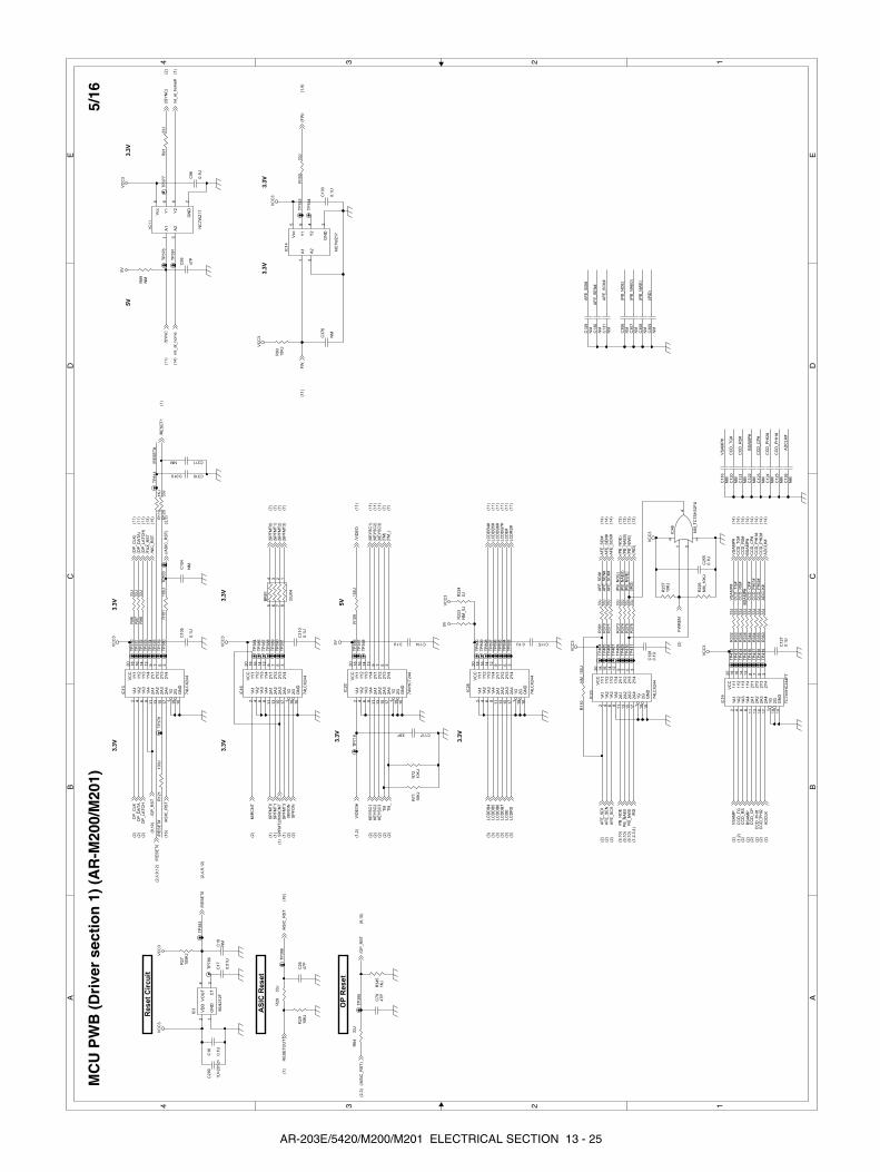
/RE
SE
T#
/RE
SE
T#
AF
E_
SD
I#A
FE
_S
EN
#
CC
D_
TG
#V
SA
MP
#
CC
D_
RS
#
CC
D_
PH
I1#
CC
D_
CP
#
AD
CL
K#
CC
D_
PH
I2#
VS
AM
P#
CC
D_
TG
#
CC
D_
RS
#
BS
AM
P#
CC
D_
CP
#
CC
D_
PH
I2#
CC
D_
PH
I1#
AD
CL
K#
BS
AM
P#AF
E_
SC
K#
(/R
D)
(PB
_N
OE
)
(PB
_N
WE
)(P
B_
NA
E0
)
AF
E_
SC
K#
(/R
D)
(PB
_N
OE
)
(PB
_N
WE
)
(PB
_N
AE
0)
AF
E_
SD
I#
AF
E_
SE
N#
VC
C3
5V
VC
C3
5V
VC
C3
VC
C3
VC
C3
VC
C3
VC
C3
VC
C3
VC
C3
VC
C3
5V
VC
C3
(OP
_D
AT
A)
(11
)(O
P_
LA
TC
H)
(11
)
(SP
FM
T0
)(7
)
OP
_C
LK
(2)
OP
_D
AT
A(2
)
SP
FM
T0
(1)
SP
FM
T1
(1)
SP
FM
T3
(1)
MIR
ON
(2)
SP
FO
N(2
)
(SP
FM
T1
)(7
)(S
PF
MT
2)
(7)
(SP
FM
T3
)(7
)
TM
(2)
TM
_(2
)
(TM
)(7
)(T
M_
)(7
)
SP
FM
T2
/MIR
CN
T(1
)
MIR
CN
T(2
)
KE
YS
C1
(2)
KE
YS
C2
(2)
KE
YS
C3
(2)
OP
_L
AT
CH
(2)
(OP
_C
LK
)(1
1)
/SY
NC
(11
)(/
SY
NC
)(2
)/A
SIC
_R
ST
(16
)(/
AS
IC_
RS
T)
(2,3
)
FW
(11
)(F
W)
(1,9
)
VID
EO
#(1
,2)
/VID
EO
(11
)
/RE
SE
T0
(2,4
,9,1
2)
/RE
SE
T1
(1)
/OP
_R
ST
(9,1
0)
/NIC
_R
ST
(15
)
/AS
IC_
RS
T(1
6)
RE
SE
TO
UT
1(1
)
/FA
X_
RS
T(1
3)
(/A
SIC
_R
ST
)(2
,3)
/OP
_R
ST
(9,1
0)
mt_
at_
ho
me
(14
)m
t_a
t_h
om
e#
(1)
AF
E_
SD
I(2
)A
FE
_S
EN
(2)
AF
E_
SC
K(2
)
AF
E_
SD
I#(1
4)
AF
E_
SE
N#
(14
)A
FE
_S
CK
#(1
4)
VS
AM
P(2
)
CC
D_
TG
(1,2
)
VS
AM
P#
(14
)C
CD
_T
G#
(14
)C
CD
_R
S(2
)
BS
AM
P(2
)
CC
D_
RS
#(1
4)
BS
AM
P#
(14
)C
CD
_C
P(2
)
CC
D_
PH
I1(2
)
CC
D_
CP
#(1
4)
CC
D_
PH
I1#
(14
)C
CD
_P
HI2
(2)
AD
CL
K(2
)
CC
D_
PH
I2#
(14
)A
DC
LK
#(1
4)
/RD
(1,2
,3,4
)PB
_N
AE
0(9
,10
)P
B_
NW
E(9
,10
)
PB
_N
OE
(9,1
0)
(PB
_N
OE
)(1
3)
(PB
_N
AE
0)
(13
)(P
B_
NW
E)
(13
)(/
RD
)(1
3)
/RE
SE
T0
(2,4
,9,1
2)
LC
DD
B4
(3)
LC
DD
B5
(3)
LC
DD
B6
(3)
LC
DD
B7
(3)
LC
DE
(3)
LC
DR
S(3
)
LC
DD
B5
#(1
1)
LC
DD
B6
#(1
1)
LC
DD
B7
#(1
1)
LC
DE
#(1
1)
LC
DR
S#
(11
)
LC
DD
B4
#(1
1)
(KE
YS
C2
)(1
1)
(KE
YS
C1
)(1
1)
(KE
YS
C3
)(1
1)
FW
RE
N(2
)
3.3V
3.3V
3.3V
5V
3.3V
3.3V
3.3V
3.3V
5V
3.3V
ResetCircuit
ASICReset
OPReset
3.3V
C1
28
0.1
U
TP
38
1
TP
71
8
R1
19
1K
J
C1
23
NM
TP
38
6
TP
39
7
TP
41
5TP
38
4
C9
9
47
P
TP
40
7
TP
37
0 C1150.1U
TP
89
5
C3
06
NM
R2
23
NM
_0
J
IC2
0
74
VH
CT
24
4
1A
12
1A
24
1A
36
1A
48
2A
11
1
2A
21
3
2A
31
5
2A
41
7
1G
1
2G
19
1Y
11
8
1Y
21
6
1Y
31
4
1Y
41
2
2Y
19
2Y
27
2Y
35
2Y
43
VC
C2
0
GN
D1
0
R3
44
33
J
IC1
6
74
LC
X2
44
1A
12
1A
24
1A
36
1A
48
2A
11
1
2A
21
3
2A
31
5
2A
41
7
1G
1
2G
19
1Y
11
8
1Y
21
6
1Y
31
4
1Y
41
2
2Y
19
2Y
27
2Y
35
2Y
43
VC
C2
0
GN
D1
0R
29
10
KJ
R3
33
33
J
C3100.01U
R3
38
33
J
C1
24
NM
R3
73
33
J
TP
89
6
TP
37
7
C2
90
1U
<2
01
2>
TP
39
0
IC2
3
74
LC
X2
44
1A
12
1A
24
1A
36
1A
48
2A
11
1
2A
21
3
2A
31
5
2A
41
7
1G
1
2G
19
1Y
11
8
1Y
21
6
1Y
31
4
1Y
41
2
2Y
19
2Y
27
2Y
35
2Y
43
VC
C2
0
GN
D1
0
TP
41
2TP
37
5
C3
07
NM
R1
01
10
0J
R3
54
33
J
R1
10
NM
_1
00
J
TP
78
6
R2
83
3J
C3
76
NM
TP
89
7
R2
24
0J
TP
39
5
C1
25
NM
R3
74
33
J
C1
05
0.1
U
R1
20
33
JR
12
11
00
J
R1
09
10
0J
TP
41
7TP
38
7
C3
08
NM
TP
40
9
TP
37
2 R3
55
33
J
TP
89
8
TP
40
4
R1
00
33
J
C2
55
0.1
U
C1
20
NM
C1
26
NM
R3
75
33
J
C1
04
NM
C1
7
0.0
1U
C311NM
TP
89
9
TP
39
6
C3
09
NM
TP
41
4TP
38
0 R3
60
33
J
TP
40
6
TP
37
8
IC4
6
NM
_T
C7
SH
32
FU
1 24
5 3
C1
27
0.1
U
TP
39
4
C2
64
7P
R3
76
33
J
TP
90
0
R6
43
3J
TP
83
3
IC2
6
74
LC
X2
44
1A
12
1A
24
1A
36
1A
48
2A
11
1
2A
21
3
2A
31
5
2A
41
7
1G
1
2G
19
1Y
11
8
1Y
21
6
1Y
31
4
1Y
41
2
2Y
19
2Y
27
2Y
35
2Y
43
VC
C2
0
GN
D1
0
TP
41
9TP
38
9
TP
41
1
TP
37
4
C1
21
NM
C1
29
NM
R3
32
33
J
R3
36
33
J
R2
71
00
KJ
R9
13
3J
TP
37
6
TP
39
8
R3
61
33
J
IC1
1
NC
7W
Z1
7
A1
1
A2
3
Y1
6
Y2
4
GN
D2
Vcc
5
TP
41
6TP
38
5
IC3 BU
42
12
F
GN
D1
VD
D2
CT
3
VO
UT
4
R9
63
3J
C1
03
0.1
U
TP
40
8
TP
37
1
TP
39
3
C1
22
NM
C1
30
NM
C1
16
NM
C11733P
R8
9N
M
BR
61
33
JX
4
1234
8765
R7
11
0K
J
TP
38
3
C1
10
0.1
U
C9
6
0.1
U
R2
26
NM
_1
0K
J
IC1
4
NC
7W
Z1
7
A1
1
A2
3
Y1
6
Y2
4
GN
D2
Vcc
5
TP
81
4
R3
70
33
J
TP
39
1
C79
47
P
TP
41
3TP
37
9
R9
73
3J
C1
31
NM
C1140.1U
R9
31
0K
J
IC1
9
TC
74
VH
C2
44
FT
1A
12
1A
24
1A
36
1A
48
2A
11
1
2A
21
3
2A
31
5
2A
41
7
1G
1
2G
19
1Y
11
8
1Y
21
6
1Y
31
4
1Y
41
2
2Y
19
2Y
27
2Y
35
2Y
43
VC
C2
0
GN
D1
0
C1
8N
M
C1
6
0.1
U
TP
89
3
R3
71
33
J
R7
21
0K
J
IC1
3
74
LC
X2
44
1A
12
1A
24
1A
36
1A
48
2A
11
1
2A
21
3
2A
31
5
2A
41
7
1G
1
2G
19
1Y
11
8
1Y
21
6
1Y
31
4
1Y
41
2
2Y
19
2Y
27
2Y
35
2Y
43
VC
C2
0
GN
D1
0
TP
41
8TP
38
8
TP
41
0
TP
37
3
R2
37
10
KJ
R9
83
3J
R3
45
1K
J
TP
40
5
TP
89
4
A A
B B
C C
D D
E E
44
33
22
11
MC
UP
WB
(Dri
ver
sect
ion
1)(A
R-M
200/
M20
1)5/
16
AR-203E/5420/M200/M201 ELECTRICAL SECTION 13 - 25

PR
#
/PR
PR
#
PG
ND
24
V
PG
ND
24
V
PG
ND
5V
VC
C3
12
V
PG
ND
VC
C3
24
VP
GN
D
24
V
INT
5V
24
V
5V
VC
C3
VC
C3
5V
VC
C3
12
V
VC
C3
VC
C3
VC
C3
VC
C3
12
V
VC
C3
12
V
12
V
12
V5
VV
CC
3
INT
24
V
PG
ND
12
V
EN
5V
VC
C3
VC
C3
EN
5V
12
V
12
V
12
V
VC
C3
EN
5V
MC
(2)
BIA
S(2
)T
C(2
)G
RID
L(2
)
/MC
(11
)/B
IAS
(11
)/T
C(1
1)
/GR
IDL
(11
)M
CN
T(3
)/M
CN
T(1
2)
PS
FM
(3)
/PO
FF
(11
)P
OF
F(1
)M
RP
S3
(2)
MR
PS
_3
(7)
SH
OL
D(1
1)
/LE
ND
CP
FS
2(2
)/C
PF
S2
(12
)M
PF
S(2
)
CP
FS
1(2
)
RR
S(2
)
VF
M_
24
V(2
)V
FM
CN
T_
12
V(2
)
MR
PS
2(2
)M
RP
S1
(2)
HL
(2)
LD
EN
PM
CL
KP
MD
MM
_Y
2M
M_
Y1
FT
H
MM
D(2
)
MM
_Y
3
/CP
FS
1(1
2)
VF
MO
UT
(12
)
HL
OU
T(1
1)
/MP
FS
(12
)
/VF
MC
NT
(12
)
/RR
S(1
2)
/PM
D(1
1)
MR
PS
_2
(7)
PM
CL
K_
A(1
1)
MM
ref1
(7)
/MM
D(1
2)
/LD
EN
(11
)
MR
PS
_1
(7)
MM
ref0
(7)
/MM
CL
K(1
2)
MM
CL
K(1
)
MM
ref2
(7)
PS
FM
OU
T(1
2)
PT
PU
LS
E(2
)
TC
S_
AN
(16
)(T
CS
_A
N)
(1)
FT
H
RT
H(1
)
TH
OP
EN
(3)
RT
H_
IN(1
2)
/PR
(11
)P
R
LC
DC
ON
T(1
)
(LC
DC
ON
T)
(11
)
AnalogTonnerSensorBuffer
LC
DC
on
tras
tB
uff
er
TP
79
5
TP
45
1
TP
43
0
TP
43
8R1
02
1K
F
TP
45
8
TP
42
8
R1
13
30
0J
R3
83
NM
TP
42
7
D5
8
RL
S-7
3
D3
6
1S
S3
55
R3
00
47
0K
J
C3
71
NM
TP
80
4
R3
03
10
KJ
TP
80
7
R2
64
12
KF
CP
17
06
03
SF
F1
50
FM
/32
-2
TP
80
1
TP
79
2
R1
18
1.2
KF
IC2
5
KID
65
00
1A
F
1B
1
2B
2
3B
3
4B
4
5B
5
6B
6
7B
7
E8
CO
M9
1C
16
2C
15
3C
14
4C
13
5C
12
6C
11
7C
10
R26610KJ
R1
17
10
KJ
TP
72
2
TP
46
3
TP
44
5
R1
14
10
0J
R3
08
NM
TP
45
9
D5
6
CR
H0
1
TP
44
8
R3
16
NM
D6
6
NM
_K
DS
22
6
213
R3
01
4.7
KJ
TP
43
7
R1
29
NM
TP
47
4
R3
87
4.7
KJ1
/4W
<3
21
6>
TP
44
9Q
16
KR
C1
02
S
1
2
3
R1
23
10
KF
Q1
5
NM
_2
SB
11
97
KB
E C
TP
45
2
IC2
7
KID
65
50
3F
1B
1
2B
2
3B
3
4B
4
5B
5
6B
6
7B
7
G8
NC
9
1C
16
2C
15
3C
14
4C
13
5C
12
6C
11
7C
10
R3
07
7.5
KF
TP
79
7
TP
78
4
TP
43
5
R4
13
NM
_1
0K
J
TP
44
4
C1
11
0.1
U/5
0V
<1
60
8>
TP
42
3
R3
81
NM
TP
43
6
D5
2
MT
ZJ2
2B
TP
44
6
Q2
0K
RA
11
9S
1
2
3
Q1
8K
RC
10
2S
1
2
3
R3
04
10
0J
TP
47
2
TP
47
0
Q3
KR
A1
19
S
1
2
3
R3
02
10
KJ
C1
13
0.1
U
R3
68
NM
TP
42
4
BR
62
1.5
KJX
4
1 2 3 4
8 7 6 5
R1
24
4.7
KJ
C4
07
NM
D6
7
KD
S2
26
213
Q1
7
KR
C1
02
S
1
2
3
R4
14
NM
_1
0K
J
TP
45
5
R3
88
47
KJ
R3
95
1.5
KJ
+ -
IC4
5A
KIA
35
8F
-EL
/P
3 21
8 4
TP
80
2
TP
72
3
TP
43
9
IC2
1
KID
65
00
1A
F
1B
1
2B
2
3B
3
4B
4
5B
5
6B
6
7B
7
E8
CO
M9
1C
16
2C
15
3C
14
4C
13
5C
12
6C
11
7C
10
R3
82
10
KJ
TP
80
5
TP
45
4
D5
1S
S3
55
C1
12
22
00
0P
TP
42
0
R1
06
10
KF
D4
1S
S3
55
R3
80
NM
_1
.5K
J
D5
9
NM
_K
DS
22
6
213
R1
42
NM
_1
0K
J
TP
79
8
D2
NM
_K
DS
22
6
213
C3
79
0.1
U
C1
19
22
00
0P
D5
5
CR
H0
1
R26810KJ
R4
18
NM
_1
0K
J
R1
04
7.5
KF
TP
47
5
R1
15
10
0J1
/4W
<3
21
6>
+ -
IC2
2A
KIA
39
3F
3 21
8 4
C1
18
0.1
U/5
0V
<1
60
8>
Q7
KT
A1
50
5S
TP
42
5
TP
45
0
Q4
KR
C1
02
S
1
2
3
TP
43
4T
P4
26
R2
97
47
KJ
Q2
1
KR
C1
02
S
1
2
3+ -
IC4
5B
KIA
35
8F
-EL
/P
5 67
8 4
+ -
IC1
7A
KIA
39
3F
3 21
8 4
TP
46
1
CP
16
06
03
SF
F1
50
FM
/32
-2
TP
47
3
TP
44
0
R3
89
47
KJ
+ -
IC5
3A
KIA
35
8F
-EL
/P
3 21
8 4
TP
79
3
TP
44
3R
10
74
.3K
F
R3
66
0J
TP
46
0
TP
42
9
TP
45
7
R3
62
4.7
KJ1
/4W
<3
21
6>
R9
01
0K
J
R3
96
1.5
KJ
TP
79
9
BR
63
1.5
KJX
4
1 2 3 4
8 7 6 5
+ -
IC2
2B
KIA
39
3F
5 67
8 4
R3
39
10
0J
TP
78
1
Q2
NM
_K
TA
15
05
S
TP
42
1
D5
7
RL
S-7
3
(G)
(D)
(S)
Q1
92
SK
30
18
C3
98
0.1
U
+ -
IC5
3B
KIA
35
8F
-EL
/P
5 67
8 4
TP
46
5
R2
98
1.5
KF
TP
80
3
Q1
32
SB
11
32
B
E C
R3
94
NM
TP
55
3
TP
80
6
TP
43
3
TP
46
4
R3
63
47
KJ
D6
0
NM
_K
DS
22
6
213
D4
5
1S
S3
55
TP
78
9
R26910KJ
TP
46
7
R26510KJ
R1
05
1K
J
+ -
IC1
7B
KIA
39
3F
5 67
8 4
R3
86
4.7
KJ1
/4W
<3
21
6>
TP
43
1
TP
45
3
D1
MA
70
0
TP
46
9
TP
44
1
IC2
4
KID
65
50
3F
1B
1
2B
2
3B
3
4B
4
5B
5
6B
6
7B
7
G8
NC
9
1C
16
2C
15
3C
14
4C
13
5C
12
6C
11
7C
10
R2
96
10
KJ
C3
05
0.1
U
TP
44
7
TP
79
4
R3
79
NM
_1
.5K
JR
11
2
NM
_4
.7K
J1
/4W
<3
21
6>
R4
19
NM
_1
0K
J
TP
80
0
TP
45
6
R27010KJ
R2
99
10
0J
Q1
22
SB
11
32
B
E C
D3
KD
S2
26
213
C3
12
1U
<2
01
2>
R1
03
1M
F
C3
67
2.2
U<
20
12
>
D6
1
1S
S3
55
R1
16
10
KJ
Q1
4
KR
C1
02
S
1
2
3
D5
1
1S
S3
55
R3
78
0J
TP
47
6
R1
08
NM
_4
7K
J
R3
93
0J
TP
46
6
TP
79
0T
P7
85
TP
43
2
TP
44
2
TP
42
2
R27110KJ
A A
B B
C C
D D
E E
44
33
22
11
MC
UP
WB
(Dri
ver
sect
ion
2)(A
R-M
200/
M20
1)6/
16
AR-203E/5420/M200/M201 ELECTRICAL SECTION 13 - 26

PG
ND
PG
ND
PG
ND
5V
24
VS
CM
T5V
5V
5V
PG
ND
PG
ND
PG
ND
PG
ND
PG
ND
PG
ND
PG
ND
PG
ND
PG
ND
24
VS
FT
MT
24
VD
up
MT
PG
ND
24V
SP
FM
T
PG
ND
5V
PG
ND
24
V
24
VS
PF
SO
L
24
VS
CM
T
24
VD
up
MT
PG
ND
24
VS
PF
MT
24
V
PG
ND
24
VS
FT
MT
24
VS
PF
SO
L
MM
_P
H_
A(2
)
OU
T_
A-
(12
)
MM
_A
I0(2
)
MM
_P
H_
B(2
)
MM
_B
I0(2
)M
M_
BI1
(2)
MM
_A
I1(2
)
OU
T_
A+
(12
)
OU
T_
B-
(12
)
MM
ref0
(6)
MM
ref1
(6)
MM
ref2
(6)
DM
T0
(1)
/DM
T0
(12)
DM
T1
(1)
DM
T2
(1)
DM
T3
(1)
/DM
T1
(12)
/DM
T2
(12)
/DM
T3
(12)
(TM
)(5
)
(TM
_)
(5)
MR
PS
_1
(6)
MR
PS
_2
(6)
MR
PS
_3
(6)
OU
T_
B+
(12
)
SF
TM
T0
(3)
/SF
TM
T0
(12
)
SF
TM
T1
(3)
SF
TM
T2
(3)
/SF
TM
T1
(12
)
/SF
TM
T2
(12
)
/SF
TM
T3
(12
)
SF
TM
T3
(3)
SP
MT
_0
(11)
(SP
FM
T0
)(5
)
SP
MT
_2
(11)
(SP
FM
T2
)(5
)
(SP
FM
T3
)(5
)(S
PF
MT
1)
(5)
SP
MT
_3
(11)
SP
MT
_1
(11)
TM
A_
O(1
2)
TM
B_
O(1
2)
/SR
VC
(11
)
SR
VC
(3)
(RS
V_
SO
L)
(3)
/RS
V_
SO
L(1
1)
SP
US
(3)
/SP
US
(11
)
ScannerMotorDriver
SPFMotorDriver
DuplexMotorDriver
ShifterMotorDriver
TonnerMotorDriver
RSPFSolenoidDriver
IC3
3
TD
62
06
4A
F
I13
NC
4
NC
5
I26
NC
10
I31
1
NC
12
NC
13
GN
D1
7
O1
2
O2
7
O3
9
O4
16
CO
M1
CO
M8
GN
D1
8
I41
4
NC
15
R1
61
62
0J
C1
40
0.1
U/5
0V
<1
60
8>
CP
60
60
3S
FF
15
0F
M/3
2-2
C1
43
0.1
U/5
0V
<1
60
8>
R1
62
1.2
KJ
R1
45
1.5
KJ
TP
48
2
TP
50
2
R1
63
10
0J
R1
43
0.6
8J
1W
R1
59
1.2
KJ
C1
33
82
0P
TP
50
5
TP
48
9
R1
46
1.5
KJ
R148
30
KJ
TP
49
2
Q23
2S
D1
78
1K
C1
38
0.1
U
R1
44
0.6
8J
1W
C1
35
820P
R1
47
1K
J
IC31
TD
62
06
4A
F
I13
NC
4
NC
5
I26
NC
10
I31
1
NC
12
NC
13
GN
D1
7
O1
2
O2
7
O3
9
O4
16
CO
M1
CO
M8
GN
D1
8
I41
4
NC
15
R1
49
30
KJ
C1
34
82
0P
TP
49
7
R4
07
10
KJ
C1
36
82
0P
BR
66
10
KJX
4
1234
8765
IC36
TA
72
91
AS
Vcc
2
IN1
9
IN2
1
GN
D5
OU
T2
3
OU
T1
7
Vre
f8
Vs
6
N.C
4
R2
75
NM
_1
.2K
J
TP
47
9
+C
13
94
7U
/35
V
TP
48
1
D8
MT
ZJ2
2B
R1
52
51
0J
C1
41
0.1
U
TP
48
4
CP
10
60
3S
FF
15
0F
M/3
2-2
TP
50
3
D4
11
SS
35
5
R1
57
1J
2W
R1
51
1K
JC
13
70.1
U
R4
08
10
KJ
R1
50
2K
J
TP
50
6
CP
20
60
3S
FF
15
0F
M/3
2-2
IC3
4
ST
A7
10
0MO
UT
A1
OU
TA
2
OU
TA
/3
OU
TA
/4
Vs
13
OU
TB
17
OU
TB
18
OU
TB
/15
OU
TB
/16
GN
D10
INA
8
INA
/7
INB
11
INB
/1
2
RE
F9
Se
nse
A5
Se
nse
B1
4
Syn
c6
TP
47
8
TP
49
4
R4
03
1.2
KJ
TP
48
8
+C
14
21
0U
/35
V
TP
50
1
Q2
42S
D1781K
TP
49
9
C1
45
0.1
U/5
0V
<1
60
8>
CP
50
60
3S
FF
15
0F
M/3
2-2
TP
48
0
R3
12
0J
<1
60
8>
IC32
L6219D
S
OU
T2
A2
SE
NS
E2
3
CO
MP
24
OU
T2
B5
GN
D6
GN
D7
I02
8
I12
9
PH
AS
E2
10
VR
EF
21
1
RC
21
2V
SS
13
RC
11
4V
RE
F1
15
PH
AS
E1
16
I11
17
GN
D1
8G
ND
19
I01
20
OU
T1
B2
1C
OM
P1
22
SE
NS
E1
23
VS
24
OU
T1
A1
R164
4.7
KJ
D4
21
SS
35
5
C1
44
NM
_1
0U
/10
V<
20
12
>
R1
60
30
0J
TP
48
5
TP
48
7
TP
50
4
R4
04
1.2
KJ
Q2
5N
M_
2S
D1
78
1K
R1
58
1J
2W
R4
06
NM
_10K
J
TP
49
1
CP
30
60
3S
FF
15
0F
M/3
2-2
D4
31
SS
35
5
TP
49
6
R3
09
NM
_0
J<
16
08
>
D9
MT
ZJ2
2B
TP
48
3
TP
47
7
A A
B B
C C
D D
E E
44
33
22
11
MC
UP
WB
(Dri
ver
sect
ion
3)(A
R-M
200/
M20
1)7/
16
AR-203E/5420/M200/M201 ELECTRICAL SECTION 13 - 27
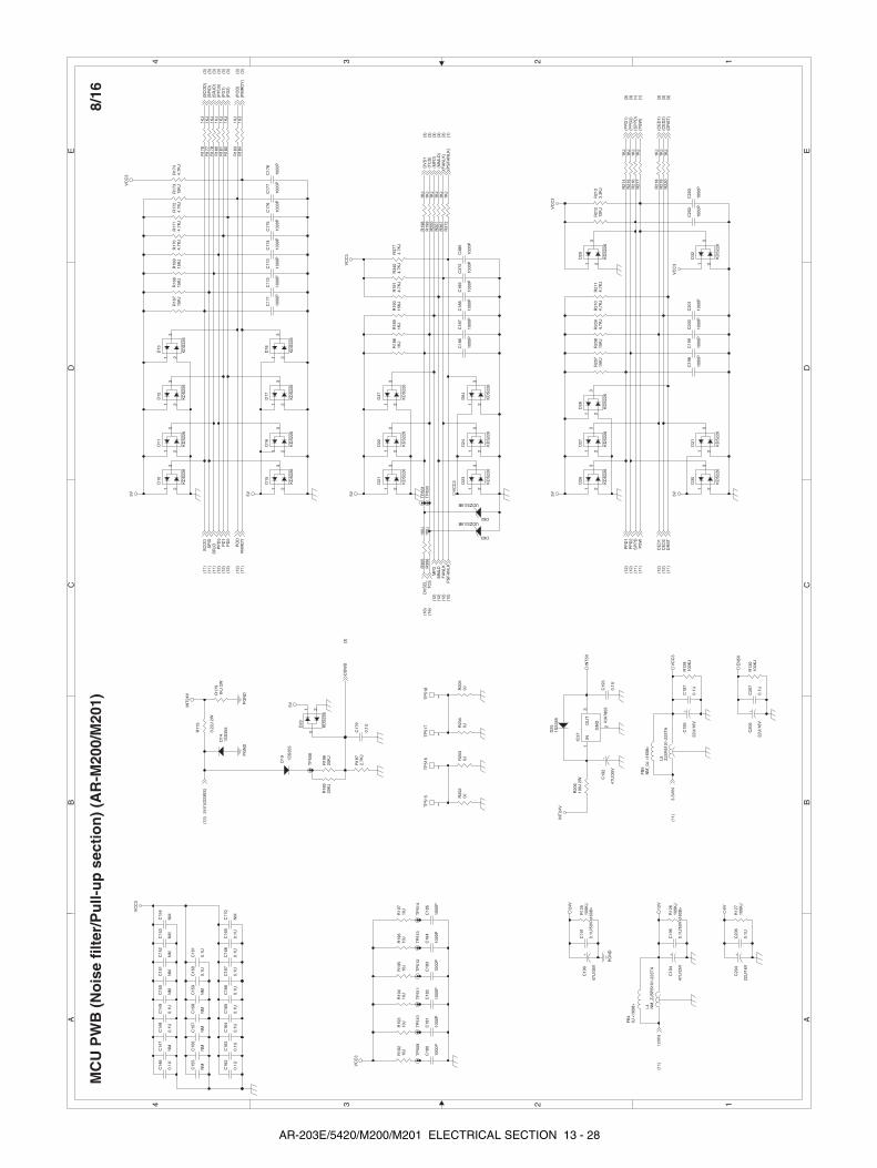
5V
5V 5V
VC
C3
24V
PG
ND
INT
24V
INT
5V
EN
5V
VC
C3
5V 5V
VC
C3
5VV
CC
3
12V
VC
C3
VC
C3
5VINT
24V
PG
ND
PG
ND
VC
C3
VC
C3
SR
JD(1
1)
PO
D(1
2)P
MR
DY
(11)
(SC
OD
)(3
)
(SR
JD)
(3)
(PO
D)
(3)
(PM
RD
Y)
(3)
TC
S(1
6)
MM
LD(1
2)
DV
S1
(3)
(MM
LD)
(3)
(TC
S)
(3)
(MF
D)
(3)
DR
ST
(11)
PS
W(1
1)S
PP
D(1
1)
(PP
D3)
(3)
3.3V
IN(1
1)
DV
SE
L(1
6)
(SP
ID)
(3)
(PP
D2)
(3)
(DR
ST
)(3
)
(SP
PD
)(1
)
(CE
D1)
(3)
CE
D2
(12)
(PS
W)
(1)
PP
D1
(12)
CE
D1
(12)
(CE
D2)
(3)
PP
D2
(12)
(PP
D1)
(3)
PD
1(1
2)P
D2
(12)
(PD
1)(3
)(P
D2)
(3)
SC
OD
(11)
PP
D3
(12)
12V
IN(1
1)
DS
WS
(3)
24V
1(D
SW
S)
(12)
(FA
NLK
)(3
)F
AN
LK(1
2)
SP
ID(1
1)
MF
D(1
2)
(PS
FA
NLK
)(1
)P
SF
AN
LK(1
2)
R18
41K
J
R19
015
KJ
R19
710
J
TP
831
R21
212
KJ
C16
4
0.1U
C19
6
0.1U
/50V
<16
08>
R20
40J
R19
14.
7KJ
R12
510
0KJ
D15
KD
S22
6
213
R21
33.
3KJ
R34
04.
7KJ
TP
508
C18
1
1000
P
C18
6
1000
P
R17
04.
7KJ
D16
KD
S22
6
213
R19
610
J
C16
5
0.1U
R30
510
0J
R20
94.
7KJ
TP
509
C18
7
1000
P
C37
2
1000
P
C17
5
1000
P
TP
517
1
D17
KD
S22
6
213
R17
5
0.22
J 2W
R37
74.
7KJ
R21
04.
7KJ
C16
6
0.1U
C18
8
1000
P
R12
810
0KJ
C18
0
1000
P
C19
9
1000
P
R20
610
0J 2
W
TP
516
1
C14
6
0.1U
C18
9
1000
P
C16
7
0.1U
FB
5N
M_0
J <
1608
>
C18
3
1000
P
C20
2
1000
P
C18
5
1000
P
R21
41K
J
C38
0
1000
P
D63
UDZS3.9B
C20
3
1000
P
C16
8
0.1U
D54
KD
S22
6
213
D21
KD
S22
6
213
TP
510
D10
KD
S22
6
213
R21
51K
J
R18
72.
7KJ
+C
204
22U
/16V
D25
1SS
355
C20
0
1000
P
C14
7
NM
D13
KD
S22
6
213
D22
KD
S22
6
213
IC37
KIA
7805
IN1
GN
D
2
OU
T3
D11
KD
S22
6
213
C18
4
1000
P
C17
4
1000
P
C16
9
0.1U
R21
61K
J
C20
6
0.1U
C20
1
1000
P
D18
KD
S22
6
213
D23
KD
S22
6
213
D12
KD
S22
6
213
R37
21K
J
C20
7
0.1U
R19
410
J
R21
71K
J
C17
0
NM
D24
KD
S22
6
213
R16
815
KJ
R17
24.
7KJ
C14
8
0.1U
+C
205
22U
/16V
C19
3
0.1U
R13
010
0KJ
R19
210
J
R21
81K
J
TP
511
R16
715
KJ
C15
7
NM
+C
192
47U
/35V
R19
81K
J
R21
91K
J
C19
7
0.1U
C17
2
1000
P
R19
91K
J
C14
9
0.1U
C15
8
NM
C17
8
1000
P
D20
KD
S22
6
213
C17
1
1000
P
L5 ZJS
R51
01-2
23T
A
R30
610
0J
R20
20J
R22
01K
J
R17
14.
7KJ
D14
1SS
355
R20
01K
J
C15
9
NM
R21
14.
7KJ
+C
195
22U
/16V
C15
1
NM T
P51
2
R20
11K
J
C15
0
NM
C16
0
0.1U
D37
KD
S22
6
213
C15
2
NM
R20
30J
C18
2
1000
P
C19
8
1000
P
R17
61K
J
C16
1
0.1U
TP
830
R18
520
KJ
D30
KD
S22
6
213
C15
3
NM
R12
610
0KJ
R20
715
KJ
R18
31K
J
D19 1S
S35
5
C17
7
1000
P
R17
71K
J
D31
KD
S22
6
213
TP
513
C15
4
NM
TP
518
1
D28
KD
S22
6
213
R17
81K
J
C17
3
1000
P
+C
194
47U
/25V
+C
190
47U
/35V
D26
KD
S22
6
213
R19
310
J
R17
91K
J 2W
R17
44.
7KJ
C15
5
NM
R18
01K
J
C19
1
0.1U
/50V
<16
08>
D29
KD
S22
6
213
L4 NM
_ZJS
R51
01-2
23T
A
R16
915
KJ D
32
KD
S22
6
213
C15
6
NM
R20
50J
C17
9
0.1U
D27
KD
S22
6
213
R18
11K
J
TP
514
C16
2
0.1U
C17
6
1000
P
R18
81K
J
FB
40J
<16
08>
R12
710
0KJ
R18
21K
J
R19
510
J
R17
315
KJ
R18
91K
J
D62
UDZS3.9B
C16
3
0.1U
R36
71K
J
R20
815
KJ
TP
515
1
R18
620
KJ
A A
B B
C C
D D
E E
44
33
22
11
MC
U P
WB
(N
ois
e fi
lter
/Pu
ll-u
p s
ecti
on
) (A
R-M
200/
M20
1)8/
16
AR-203E/5420/M200/M201 ELECTRICAL SECTION 13 - 28

_S
DR
AM
_C
LK
SD
RA
M_
DA
TA
0
SD
RA
M_
DA
TA
5
_S
DR
AM
_D
QM
A0
_S
DR
AM
_C
KE
RO
M_
CS
_L
SD
RA
M_
DQ
MA
1
SD
RA
M_
DA
TA
11
_S
DR
AM
_D
QM
B1
SD
RA
M_
DA
TA
10
SD
RA
M_
RA
S_
L
SD
RA
M_
CK
E
XO
UT
SD
RA
M_
DA
TA
6
SD
RA
M_
CA
S_
L
SD
RA
M_
DA
TA
15
SD
RA
M_
DA
TA
9
SD
RA
M_
CS
0_
L
SD
RA
M_
CA
S_
L
RO
M_
CS
_L
_S
DR
AM
_D
QM
A1
_S
DR
AM
_D
QM
A1
_S
DR
AM
_D
QM
B0
SD
RA
M_
DQ
MB
0S
DR
AM
_W
E_
L
SD
RA
M_
DQ
MA
0
_S
DR
AM
_D
QM
A0
SD
RA
M_
BA
NK
0
SD
RA
M_
DA
TA
8
SD
RA
M_
DA
TA
12
SD
RA
M_
DA
TA
14
SD
RA
M_
DA
TA
3S
DR
AM
_D
AT
A2
SD
RA
M_
DA
TA
4
SD
RA
M_
DA
TA
7
SD
RA
M_
DA
TA
13
SD
RA
M_
BA
NK
1
SD
RA
M_
DQ
MB
1
_S
DR
AM
_C
S0
_L
SD
RA
M_
DA
TA
1
TR
ST
_L
TC
KT
MS
SD
RA
M_
RA
S_
L
SD
RA
M_
WE
_L
SD
RA
M_
RA
S_
LS
DR
AM
_C
AS
_L
_S
DR
AM
_D
QM
A0
_S
DR
AM
_C
S0
_L
SD
RA
M_
WE
_L
_S
DR
AM
_C
KE
TD
I
CL
K_
EX
T
PB
_A
DD
R3
PB
_A
DD
R0
PB
_A
DD
R6
PB
_A
DD
R1
PB
_A
DD
R4
PB
_A
DD
R7
PB
_A
DD
R5
PB
_A
DD
R2
RY
_B
Y
TD
O
PB
_D
AT
A4
PB
_D
AT
A1
PB
_D
AT
A0
PB
_D
AT
A5
PB
_D
AT
A6
PB
_D
AT
A7
PB
_D
AT
A2
PB
_D
AT
A3
TR
ST
_L
TD
IT
MS
TC
KT
DO
PID
AT
A1
PID
AT
A0
PID
AT
A2
PID
AT
A4
RY
_B
Y
PID
AT
A6
PID
AT
A7
PID
AT
A3
PID
AT
A5
SD
RA
M_
AD
DR
12
SD
RA
M_
AD
DR
11
SD
RA
M_
AD
DR
6
SD
RA
M_
AD
DR
3
SD
RA
M_
AD
DR
8
SD
RA
M_
AD
DR
12
SD
RA
M_
AD
DR
4
SD
RA
M_
AD
DR
0
SD
RA
M_
AD
DR
0
SD
RA
M_
AD
DR
1
SD
RA
M_
AD
DR
2
SD
RA
M_
AD
DR
9
SD
RA
M_
AD
DR
9
SD
RA
M_
AD
DR
7
SD
RA
M_
AD
DR
2
SD
RA
M_
AD
DR
5
SD
RA
M_
AD
DR
5
SD
RA
M_
AD
DR
3
SD
RA
M_
AD
DR
6
SD
RA
M_
AD
DR
10
SD
RA
M_
AD
DR
7
SD
RA
M_
AD
DR
11
SD
RA
M_
AD
DR
4
SD
RA
M_
AD
DR
8
SD
RA
M_
AD
DR
10
SD
RA
M_
AD
DR
1
_S
DR
AM
_C
KE
_S
DR
AM
_C
S0
_L
_S
DR
AM
_D
QM
A1
/FP
OF
F
/FP
OF
F
_S
DR
AM
_D
QM
B1
SD
RA
M_
BA
NK
0S
DR
AM
_B
AN
K1
_S
DR
AM
_D
AT
A0
_S
DR
AM
_D
AT
A1
_S
DR
AM
_D
AT
A2
_S
DR
AM
_D
AT
A4
_S
DR
AM
_D
AT
A5
_S
DR
AM
_D
AT
A6
_S
DR
AM
_D
AT
A7
_S
DR
AM
_D
AT
A8
_S
DR
AM
_D
AT
A9
_S
DR
AM
_D
AT
A1
0_
SD
RA
M_
DA
TA
11
_S
DR
AM
_D
AT
A1
2_
SD
RA
M_
DA
TA
13
_S
DR
AM
_D
AT
A1
4_
SD
RA
M_
DA
TA
15
_S
DR
AM
_C
LK
_S
DR
AM
_C
LK
_S
DR
AM
_D
AT
A3
PO
DA
TA
4P
OD
AT
A5
PO
DA
TA
7P
OD
AT
A6
PO
DA
TA
3P
OD
AT
A2
PO
DA
TA
1P
OD
AT
A0
_S
DR
AM
_D
QM
B0
SD
RA
M_
AD
DR
0S
DR
AM
_A
DD
R1
SD
RA
M_
AD
DR
2S
DR
AM
_A
DD
R3
SD
RA
M_
AD
DR
4S
DR
AM
_A
DD
R5
SD
RA
M_
AD
DR
6S
DR
AM
_A
DD
R7
SD
RA
M_
AD
DR
8S
DR
AM
_A
DD
R9
SD
RA
M_
AD
DR
10
SD
RA
M_
AD
DR
11
SD
RA
M_
AD
DR
12
SD
RA
M_
BA
NK
0S
DR
AM
_B
AN
K1
RY
_B
Y
XIN
_S
DR
AM
_D
AT
A3
_S
DR
AM
_D
AT
A1
_S
DR
AM
_D
AT
A7
SD
RA
M_
AD
DR
5S
DR
AM
_A
DD
R6
SD
RA
M_
AD
DR
8S
DR
AM
_A
DD
R9
SD
RA
M_
AD
DR
11
SD
RA
M_
AD
DR
12
SD
RA
M_
BA
NK
0S
DR
AM
_B
AN
K1
_S
DR
AM
_D
AT
A1
0_
SD
RA
M_
DA
TA
9
_S
DR
AM
_D
AT
A1
2
_S
DR
AM
_D
AT
A7
_S
DR
AM
_D
AT
A5
_S
DR
AM
_D
AT
A0
SD
RA
M_
RA
S_
LS
DR
AM
_C
AS
_L
_S
DR
AM
_C
LK
_S
DR
AM
_C
LK
_S
DR
AM
_D
QM
A0
SD
RA
M_
AD
DR
10
SD
RA
M_
AD
DR
7
SD
RA
M_
AD
DR
3 _S
DR
AM
_C
S1
A_
LS
DR
AM
_W
E_
L
SD
RA
M_
AD
DR
1S
DR
AM
_A
DD
R0 _S
DR
AM
_C
KE
_S
DR
AM
_D
QM
A1
SD
RA
M_
AD
DR
2
SD
RA
M_
AD
DR
4
_S
DR
AM
_D
AT
A2
_S
DR
AM
_D
AT
A6
_S
DR
AM
_D
AT
A1
4
_S
DR
AM
_D
AT
A6
_S
DR
AM
_D
AT
A3
_S
DR
AM
_D
AT
A0
_S
DR
AM
_D
AT
A2
_S
DR
AM
_D
AT
A1
0_
SD
RA
M_
DA
TA
5
_S
DR
AM
_D
AT
A1
_S
DR
AM
_D
AT
A1
_S
DR
AM
_D
AT
A6
_S
DR
AM
_D
AT
A1
5
_S
DR
AM
_D
AT
A1
0
_S
DR
AM
_D
AT
A4
_S
DR
AM
_D
AT
A4
_S
DR
AM
_D
AT
A7
_S
DR
AM
_D
AT
A1
1
_S
DR
AM
_D
AT
A0
_S
DR
AM
_D
AT
A7
_S
DR
AM
_D
AT
A8
_S
DR
AM
_D
AT
A1
2
_S
DR
AM
_D
AT
A0
_S
DR
AM
_D
AT
A8
_S
DR
AM
_D
AT
A3
_S
DR
AM
_D
AT
A1
4
_S
DR
AM
_D
AT
A1
2
_S
DR
AM
_D
AT
A9
_S
DR
AM
_D
AT
A1
3
_S
DR
AM
_D
AT
A5
_S
DR
AM
_D
AT
A1
5
_S
DR
AM
_D
AT
A1
_S
DR
AM
_D
AT
A9
_S
DR
AM
_D
AT
A3
_S
DR
AM
_D
AT
A5
_S
DR
AM
_D
AT
A6
_S
DR
AM
_D
AT
A8
_S
DR
AM
_D
AT
A1
1
_S
DR
AM
_D
AT
A1
1
_S
DR
AM
_D
AT
A2
_S
DR
AM
_D
AT
A4
_S
DR
AM
_D
AT
A2
_S
DR
AM
_D
AT
A8
_S
DR
AM
_D
AT
A1
5_
SD
RA
M_
DA
TA
14
_S
DR
AM
_D
AT
A1
3
_S
DR
AM
_D
AT
A1
3
_S
DR
AM
_D
AT
A4
_S
DR
AM
_C
S1
A_
L
SD
RA
M_
CS
1A
_L
_S
DR
AM
_C
S1
A_
L
VC
C3
OA
3.3
V
OA
3.3
V
OA
3.3
V
VC
C3
VC
C3
VC
C3
VC
C3
VC
C3
VC
C3
VC
C3
VC
C3
VC
C3
OA
3.3
V
VC
C3
VC
C3
VC
C3
/PO
AC
K(2
)
_S
DR
AM
_C
LK
CL
K_
EX
T
_S
DR
AM
_C
LK
/PO
RE
Q(2
)
/SC
_L
INE
(2)
CL
K_
EX
T
ES
_C
MD
(1)
ES
_S
TS
(1)
DT
_R
EQ
B(1
0)
DT
_A
CK
B(1
0)
PB
_D
AT
A[7
:0]
(10
,13
)P
B_
NC
S1
(13
)
PB
_A
DD
R[7
:0]
(10
,13
)
PB
_N
CS
3(1
0)
PB
_N
AE
0(5
,10
)
PB
_N
OE
(5,1
0)
PB
_N
WE
(5,1
0)
/PR
_L
INE
(2)
/ES
_P
AG
E(1
)
/IM
C_
RE
AD
Y(2
)
SD
RA
M_
BA
NK
[1:0
]
_S
DR
AM
_D
AT
A[1
5:0
]
SD
RA
M_
BA
NK
[1:0
]
_S
DR
AM
_D
AT
A[1
5:0
]
SD
RA
M_
AD
DR
[12
:0]
_S
DR
AM
_D
AT
A[1
5:0
]
SD
RA
M_
BA
NK
[1:0
]
/ES
_C
RD
Y(3
)
INT
_U
SB
D(1
0)
WA
KE
UP
(10
)
SU
SP
EN
D(U
SB
2.0
)(1
0)
(FW
)(1
,5)
SD
RA
M_
AD
DR
[12
:0]
/H_
SY
NC
(2)
PO
DA
TA
[7..0
](2
)
MD
M_
IRQ
(13
)
PID
AT
A[7
..0
](2
)/P
IRE
Q(2
)
/PIA
CK
(2)
/PIW
R(2
)
SD
RA
M_
AD
DR
[12
:0]
SD
RA
M_
AD
DR
[12
:0]
TC
K(1
2)
TM
S(1
2)
TD
I(1
2)
/FP
OF
F(2
)
MO
DE
M_
IN(1
3)
/RE
SE
T0
(2,4
,5,1
2)
OA
_T
X(1
2)
OA
_R
X(1
2)
TD
O(1
2)
VP
P(4
)
/ES
_S
RD
Y(1
)
/OP
_R
ST
(5,1
0) /R
ES
_O
A9
82
(1)
/RE
SE
T0
(2,4
,5,1
2)
OA
98
2_
RE
AD
Y(1
2)
TR
ST
_L
(12
)
_S
DR
AM
_D
AT
A[1
5:0
]
_S
DR
AM
_C
LK
SD
RA
M_
AD
DR
[12
:0]
_S
DR
AM
_D
AT
A[1
5:0
]
SD
RA
M_
BA
NK
[1:0
]
8M
/16M
Fla
sh
RO
M
TP
76
9
TP
56
7
TP
52
3
C2
36
0.1
U
C2
65
NM
TP
58
0
C2
64
0.1
U
TP
61
7
R1
37
33
J
FB
60
J<
16
08
>
TP
59
0
R2
35
33
J
BR
67
10
0JX
41 2 3 4
5678
C38312P
TP
91
1
TP
76
5T
P7
49
TP
57
3
C2
27
0.1
U
TP
73
3
TP
65
5
TP
63
2
TP
61
3
C2
37
0.1
U
TP
52
4
R233NM
TP
76
1
TP
53
8
C3
01
0.1
U
C3
03
NM
TP
77
4
TP
55
2
TP
77
9
TP
56
6
TP
75
6
TP
60
7
TP
90
2
TP
75
3
R2
47
4.7
KJ
C2
09
0.1
U
BR
76
33
JX
41 2 3 4
5678
TP
66
3
L6
NM
_Z
JS
R5
10
1-2
23
TA
R3
46
10
KJ
TP
60
5
TP
59
5
TP
55
9
C38412P
TP
57
7
TP
62
4
TP
60
0
TP
79
6
TP
53
3
BR
77
33
JX
4
1 2 3 45678
R23110KJ
TP
65
3
TP
80
9
TP
65
9
TP
59
1
BR
75
33
JX
41 2 3 4
5678
R2
50
4.7
KJ
C2
28
0.1
U
C2
25
0.1
U
TP
62
0
R1
38
NM
TP
76
8
TP
53
2
TP
52
5
R2
25
33
J
BR
82
10
KJX
41 2 3 4
5678
IC4
0
HY
57
V5
61
62
0F
TP
-H-C
VS
S5
4
RA
S1
8
WE
16
CA
S1
7
VS
S4
1
VS
S2
8
VD
D1
VD
D1
4V
DD
27
BA
02
0
BA
12
1
A0
23
A1
24
A2
25
A3
26
A4
29
A5
30
A6
31
A7
32
A8
33
A9
34
A1
02
2
A1
13
5
VD
DQ
3V
DD
Q9
VD
DQ
43
VD
DQ
49
VS
SQ
6V
SS
Q1
2V
SS
Q4
6V
SS
Q5
2
DQ
02
DQ
14
DQ
25
DQ
37
DQ
48
DQ
51
0
DQ
61
1
DQ
71
3
DQ
84
2
DQ
94
4
DQ
10
45
DQ
11
47
DQ
12
48
DQ
13
50
DQ
14
51
DQ
15
53
LD
QM
15
UD
QM
39
CS
19
CLK
38
CK
E3
7
A1
23
6
N.C
40
TP
77
3
TP
58
5
TP
54
6
IC4
4
HY
57
V5
61
62
0F
TP
-H-C
VS
S5
4
RA
S1
8
WE
16
CA
S1
7
VS
S4
1
VS
S2
8
VD
D1
VD
D1
4V
DD
27
BA
02
0
BA
12
1
A0
23
A1
24
A2
25
A3
26
A4
29
A5
30
A6
31
A7
32
A8
33
A9
34
A1
02
2
A1
13
5
VD
DQ
3V
DD
Q9
VD
DQ
43
VD
DQ
49
VS
SQ
6V
SS
Q1
2V
SS
Q4
6V
SS
Q5
2
DQ
02
DQ
14
DQ
25
DQ
37
DQ
48
DQ
51
0
DQ
61
1
DQ
71
3
DQ
84
2
DQ
94
4
DQ
10
45
DQ
11
47
DQ
12
48
DQ
13
50
DQ
14
51
DQ
15
53
LD
QM
15
UD
QM
39
CS
19
CLK
38
CK
E3
7
A1
23
6
N.C
40
TP
75
9
TP
58
2
C2
42
0.1
U
R3
43
NM
_0
J
TP
64
5
TP
61
8
R3
69
NM
TP
79
1
TP
78
0
TP
66
7
C38512P
C2
48
0.1
U
TP
92
5
TP
57
5
TP
75
0
TP
59
2
TP
56
1
TP
63
3
TP
61
4
R2
39
10
KJ
R2
38
10
KJ
C2
11
NM
C2
47
0.1
U
R2
27
33
J
C2
49
0.1
U
C2
24
0.1
U
TP
56
8
TP
93
0
TP
62
9
TP
60
9
TP
78
7
TP
52
6
TP
51
9
C2
30
0.1
U
C2
50
0.1
U
TP
76
4
TP
54
0 C2
41
0.1
U
R2
34
33
J
TP
55
4
TP
66
4
R2
32
NM
TP
77
2
TP
57
0
TP
56
0
C38612P
TP
92
6
TP
62
5
TP
60
2
C2
20
0.1
U
TP
91
0
TP
59
7
TP
53
5
TP
57
9
TP
65
4
C2
99
0.1
U
TP
66
0
C2
19
0.1
U
C2
39
NM
C2
13
1U
<2
01
2>
TP
77
8
TP
75
4
TP
72
8
TP
64
2
TP
55
1
C2
52
33
P
TP
62
1
TP
59
3
TP
60
8
TP
52
7
C2
35
0.1
U
C2
23
0.1
U
R2
48
4.7
KJ
TP
75
7
TP
65
0
TP
54
9T
P9
01
TP
80
8
TP
76
7
TP
65
6
TP
58
4
R2
28
33
J
TP
58
7
TP
66
8
TP
64
6
TP
63
8
R2
45
NM
C2
26
0.1
U
TP
52
0
TP
54
7
C2
15
1U
<2
01
2>
TP
53
4
TP
76
2
TP
73
0
TP
54
8
TP
56
3
TP
57
6
TP
54
5
C2
40
0.1
U
TP
63
4
TP
61
5
TP
78
8
R2
22
33
J
R3
42
4.7
KJ
TP
60
1
TP
54
3
C36212P
TP
77
1
TP
75
1
TP
56
9
TP
61
1
TP
54
1
C2
46
0.1
U
BR
78
33
JX
41 2 3 4
5678
C2
44
0.1
U
C2
16
NM
C1
00
10
00
P
C2
22
0.1
U
R2
46
NM
R2
29
33
J
R2
36
4.7
KJ
TP
66
5
TP
53
9
C2
53
47
P
BR
69
10
0JX
41 2 3 4
5678
C3
95
10
U/1
0V
<2
01
2>
TP
56
2
BR
81
33
JX
4
1 2 3 4
8 7 6 5
R2
49
0J
TP
62
6
TP
60
4
TP
57
2
TP
52
8
TP
53
7
TP
76
0
TP
54
2
R2
21
NM
TP
55
6
TP
66
1
BR
80
33
JX
4
1 2 3 4
8 7 6 5
C3
00
0.1
U
TP
64
3
C21022000P
R2
40
10
KJ
C36612P
TP
59
9
TP
62
2
TP
59
6
TP
91
2
TP
61
0
TP
58
1
TP
52
9
C2
51
NM
TP
73
1
TP
65
1C
22
10
.1U
TP
65
7
TP
58
6
BR
72
33
JX
41 2 3 4
5678
R2
43
10
KJ
C2
38
0.1
U
TP
64
7
TP
63
9
C2
18
0.1
U
R3
51
10
KJ
C3
02
0.1
U
BR
68
10
0JX
41 2 3 4
5678
C2
14
0.0
1U
R230NM
TP
52
1
C2
43
0.1
U
TP
76
6
TP
56
5
C2
45
0.1
U
R2
41
10
KJ
X4
AT
-49
(18
.38
56
MH
z)
TP
90
9
TP
77
0T
P7
55
TP
58
8
TP
57
8
BR
71
33
JX
41 2 3 4
5678
C2
31
0.1
U
C2
56
0.1
U
TP
74
5
TP
61
6
C2
17
10
U/1
0V
<2
01
2>
TP
52
2
C2
34
0.1
U
C3
96
10
U/1
0V
<2
01
2>
TP
77
7
TP
53
6
R2
42
10
KJ
C38112P
TP
55
0
IC3
8
OA
-98
2
GP
_C
0/P
B_
AD
DR
01
99
GP
_C
1/P
B_
AD
DR
12
01
GP
_C
2/P
B_
AD
DR
22
02
GP
_C
3/P
B_
AD
DR
32
03
GP
_C
4/P
B_
AD
DR
42
04
GP
_C
5/P
B_
AD
DR
52
05
GP
_C
6/P
B_
AD
DR
62
07
GP
_C
7/P
B_
AD
DR
72
08
RE
G_
A9
/PB
_N
CS
11
78
RE
G_
A8
/PB
_N
CS
21
80
GP
_A
12
6
GP
_A
2/D
C_
CH
Y1
28
GP
_A
3/D
C_
CH
X1
29
GP
_A
4/D
C_
PW
M1
30
GP
_A
5/D
C_
CH
Y0
31
GP
_A
6/D
C_
CH
X0
32
GP
_A
02
4
GP
_A
7/D
C_
PW
M0
34
GP
_B
0/U
SA
RT
0_
TX
1
GP
_B
1/U
SA
RT
0_
RX
2
GP
_B
2/U
SA
RT
0_
CK
8
GP
_B
3/A
NA
_S
D1
9
GP
_B
4/D
T_
AC
KB
11
GP
_B
5/D
T_
RE
QB
12
GP
_B
6/D
T_
AC
KA
13
GP
_B
7/D
T_
RE
QA
14
GP
_D
0/A
DC
_A
01
5
GP
_D
1/A
DC
_A
11
6
GP
_D
2/A
DC
_A
21
9
GP
_D
3/A
DC
_C
LK
21
RE
G_
AD
0/P
B_
DA
TA
01
89
RE
G_
AD
1/P
B_
DA
TA
11
88
RE
G_
AD
2/P
B_
DA
TA
21
87
RE
G_
AD
3/P
B_
DA
TA
31
86
RE
G_
AD
4/P
B_
DA
TA
41
85
RE
G_
AD
5/P
B_
DA
TA
51
83
RE
G_
AD
6/P
B_
DA
TA
61
82
RE
G_
AD
7/P
B_
DA
TA
71
81
RE
G_
AD
DR
_V
AL
ID/P
B_
NC
S0
19
0
RE
G_
RD
_L
/PB
_N
CS
31
94
RE
G_
WR
_L
/PB
_N
AE
01
95
RE
G_
CS
_L
/PB
_N
AE
11
96
RE
G_
RD
Y/P
B_
NW
E1
97
VS
S_
CO
RE
19
1
VS
S_
IO1
50
VS
S_
CO
RE
17
3
VS
S_
IO1
36
VS
S_
CO
RE
12
1
VS
S_
IO1
23
VS
S_
CO
RE
13
9
VS
S_
CO
RE
87
VS
S_
IO1
08
VS
S_
CO
RE
69
VS
S_
IO9
8
VS
S_
CO
RE
35
VS
S_
IO8
6
VS
S_
CO
RE
17
VS
S_
IO7
6V
SS
_IO
64
VS
S_
IO5
4
VS
S_
IO2
06
VS
S_
IO4
1
VS
S_
IO1
93
VS
S_
IO2
7V
SS
_IO
10
VS
S_
IO1
79
VS
S_
IO1
64
INT
ER
RU
PT
_L
/PB
_N
OE
19
8
RE
SE
T_
L1
12
TC
K1
14
TM
S1
16
TD
I1
17
TD
O1
13
BA
SE
_C
LK
/GP
_P
WM
11
68
MA
IN_
CL
K/G
P_
PW
M0
17
0C
LK
_E
XT
/GP
_P
WM
21
69
TE
ST
_M
OD
E0
17
2
XIN
5
XO
UT
4
PP
_H
IDR
IVE
/US
AR
T1
_R
X1
43
PP
_D
RIV
E/U
SA
RT
1_
TX
14
5
PP
_N
INIT
14
6
PP
_N
FA
UL
T1
47
PP
_N
SE
LE
CT
IN1
51
PP
_N
AU
TO
FD
15
2
PP
_S
EL
EC
T1
53
PP
_P
ER
RO
R1
54
PP
_B
US
Y1
55
PP
_N
AC
K1
56
PP
_D
AT
A7
15
7
PP
_D
AT
A6
15
9
PP
_D
AT
A5
16
0
PP
_D
AT
A4
16
1
PP
_D
AT
A3
16
2
PP
_D
AT
A2
16
3
PP
_D
AT
A1
/US
AR
T1
_C
K1
65
PP
_D
AT
A0
16
6
PP
_N
ST
RO
BE
16
7
PO
_L
INE
_S
YN
C/A
NA
_S
CL
K3
7
PO
_P
AG
E_
SY
NC
/AN
A_
NC
S3
8
PO
_R
EQ
/AN
A_
SD
03
9
PO
_A
CK
/PD
AT
A0
/PD
S0
40
PO
_D
ON
E/P
DA
TA
2/P
DS
24
2
PO
_W
R/P
DA
TA
1/P
DS
14
3
PO
_D
AT
A7
/LH
EA
T/P
AS
_M
44
PO
_D
AT
A6
/LC
TR
L/C
FIR
E2
45
PO
_D
AT
A5
/AG
AT
E/C
FIR
E1
47
PO
_D
AT
A4
/AC
LK
/MF
IRE
24
8
PO
_D
AT
A3
/PE
NA
BL
E/M
FIR
E1
49
PO
_D
AT
A2
/PL
OA
D5
0
PO
_D
AT
A1
/PC
LK
51
PO
_D
AT
A0
/PD
AT
A3
/PA
S_
C5
2
PI_
LIN
E_
SY
NC
/GP
_D
61
19
PI_
TR
_T
GE
N1
20
PI_
TG
EN
61
24
PI_
TG
EN
51
25
PI_
TG
EN
41
26
PI_
TG
EN
31
27
PI_
TG
EN
21
28
PI_
TG
EN
11
29
PI_
TG
EN
01
31
PI_
DA
TA
71
32
PI_
DA
TA
61
33
PI_
DA
TA
51
34
PI_
DA
TA
41
35
PI_
DA
TA
31
37
PI_
DA
TA
21
38
PI_
DA
TA
11
41
PI_
DA
TA
01
42
SD
RA
M_
DA
TA
15
53
SD
RA
M_
DA
TA
14
55
SD
RA
M_
DA
TA
13
56
SD
RA
M_
DA
TA
12
57
SD
RA
M_
DA
TA
11
58
SD
RA
M_
DA
TA
10
60
SD
RA
M_
DA
TA
96
1S
DR
AM
_D
AT
A8
62
SD
RA
M_
DA
TA
76
3S
DR
AM
_D
AT
A6
65
SD
RA
M_
DA
TA
56
6S
DR
AM
_D
AT
A4
67
SD
RA
M_
DA
TA
36
8S
DR
AM
_D
AT
A2
72
SD
RA
M_
DA
TA
17
3S
DR
AM
_D
AT
A0
74
RO
M_
CS
_L
75
SD
RA
M_
CS
1B
_L
77
SD
RA
M_
CK
E7
8S
DR
AM
_C
LK
79
SD
RA
M_
AD
DR
11
82
SD
RA
M_
BA
NK
18
3S
DR
AM
_B
AN
K0
84
SD
RA
M_
AD
DR
10
85
SD
RA
M_
AD
DR
98
9S
DR
AM
_A
DD
R8
90
SD
RA
M_
AD
DR
79
1S
DR
AM
_A
DD
R6
92
SD
RA
M_
AD
DR
59
4S
DR
AM
_A
DD
R4
95
SD
RA
M_
AD
DR
39
6S
DR
AM
_A
DD
R2
97
SD
RA
M_
AD
DR
19
9S
DR
AM
_A
DD
R0
10
0
SD
RA
M_
RA
S_
L1
01
SD
RA
M_
CS
1A
_L
10
2S
DR
AM
_C
S0
_L
10
4
SD
RA
M_
DQ
MB
11
05
SD
RA
M_
DQ
MA
11
06
SD
RA
M_
DQ
MB
01
07
SD
RA
M_
DQ
MA
01
09
SD
RA
M_
CA
S_
L1
10
SD
RA
M_
WE
_L
11
1
VD
D_
IO1
44
VD
D_
CO
RE
19
2
VD
D_
IO1
30
VD
D_
CO
RE
17
4
VD
D_
IO1
15
VD
D_
CO
RE
14
0
VD
D_
IO1
03
VD
D_
CO
RE
12
2
VD
D_
IO9
3
VD
D_
CO
RE
88
VD
D_
IO8
1
VD
D_
CO
RE
70
VD
D_
IO7
1
VD
D_
CO
RE
36
VD
D_
IO5
9
VD
D_
CO
RE
18
VD
D_
IO4
6
VD
D_
IO2
00
VD
D_
IO3
3
VD
D_
IO1
84
VD
D_
IO2
0
VD
D_
IO1
71
VD
D_
IO3
VD
D_
IO1
58
PL
LC
S_
VD
DA
7
PL
LC
S_
VS
SA
6
SD
RA
M_
AD
DR
12
80
US
B_
DP
17
6U
SB
_D
M1
75
PL
LS
S_
VD
DA
14
9
PL
LS
S_
VS
SA
14
8
TE
ST
_M
OD
E1
17
7
TR
ST
_L
11
8
GP
_D
4/A
DC
_D
AT
A2
2
GP
_D
5/A
DC
_N
CS
23
VD
D_
IO2
5
TP
74
8
IC3
9
GN
D2
7G
ND
46
VC
C3
7
IO0
29
IO1
31
IO2
33
IO3
35
IO4
38
IO5
40
IO6
42
IO7
44
IO8
30
IO9
32
IO1
03
4
IO1
13
6
IO1
23
9
IO1
34
1
IO1
44
3
IO1
5/A
-14
5
A0
25
A1
24
A2
23
A3
22
A4
21
A5
20
A6
19
A7
18
A8
8
A9
7
A1
06
A1
15
A1
24
A1
33
A1
42
A1
51
A1
64
8
A1
71
7
A1
81
6
VC
CW
13
WE
11
RE
SE
T1
2
BY
TE
47
CE
26
OE
28
RY
/BY
15
A1
99
A2
01
0
WP
/AC
C1
4
TP
57
1
C2
12
0.0
1U
TP
63
1
TP
61
2
TP
81
0
R2
44
NM
_1
0K
J
BR
73
33
JX
41 2 3 4
5678
TP
75
8
TP
75
2
BR
74
33
JX
41 2 3 4
5678
TP
56
4
TP
77
6
TP
73
2
TP
59
4
TP
60
6
TP
55
7
BR
70
10
0JX
41 2 3 4
5678
C2
63
0.1
U
TP
66
6
C2
33
0.1
U
TP
57
4
TP
66
2
BR
79
33
JX
4
1 2 3 45678
TP
64
4
C2
54
33
P
BR
83
10
KJX
41 2 3 4
5678
C38212P
R3
90
33
J
TP
66
9
TP
62
3
TP
59
8
C2
08
NM
TP
53
0T
P5
31
TP
54
4
TP
65
2
BR
84
10
KJX
41 2 3 4
5678
TP
58
3
TP
55
8
TP
65
8
TP
58
9
C3
97
10
U/1
0V
<2
01
2>
TP
76
3
TP
60
3
TP
64
8
TP
64
0
TP
77
5
TP
74
4
TP
61
9
C2
29
0.1
UC
23
20
.1U
BR
85
10
KJX
41 2 3 4
5678
A A
B B
C C
D D
E E
44
33
22
11
MC
UP
WB
(IM
C2
sect
ion
1/2)
(AR
-M20
0/M
201)
9/16
AR-203E/5420/M200/M201 ELECTRICAL SECTION 13 - 29
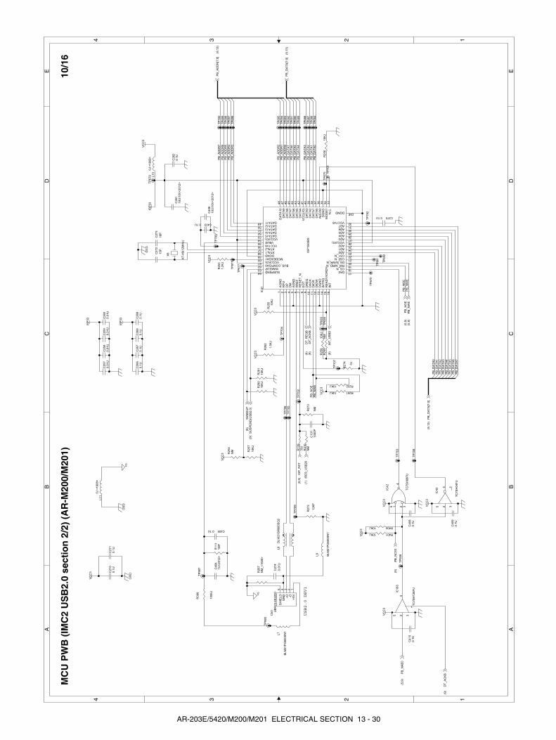
PB
_N
OE
PB
_A
DD
R0
PB
_A
DD
R5
PB
_A
DD
R1
PB
_A
DD
R2
PB
_A
DD
R3
PB
_D
AT
A1
PB
_D
AT
A0
PB
_D
AT
A0
PB
_D
AT
A4
PB
_D
AT
A4
PB
_D
AT
A3
PB
_D
AT
A1
PB
_D
AT
A7
PB
_D
AT
A6
PB
_D
AT
A5
PB
_D
AT
A3
PB
_D
AT
A5
PB
_D
AT
A2
PB
_D
AT
A7
PB
_D
AT
A6
PB
_D
AT
A2
PB
_A
DD
R4
PB
_A
DD
R6
PB
_A
DD
R7
PB
_N
WE
PB
_N
OE
PB
_N
WE
FG
ISP
33
VC
C3
ISP
33
VC
C3
VC
C3
VC
C3
VC
C3
ISP
33
FG
VC
C3
VC
C3
VC
C3
VC
C3
VC
C3
VC
C3
PB
_D
AT
A[7
:0]
(9,1
3)
PB
_N
WE
(5,9
)
DT
_R
EQ
B(9
)
PB
_D
AT
A[7
:0]
(9,1
3)
DT
_A
CK
B(9
)
INT
_U
SB
D(9
)
PB
_N
CS
3(9
)
PB
_N
OE
(5,9
)
PB
_A
DD
R[7
:0]
(9,1
3)
PB
_N
AE
0(5
,9)
/OP
_R
ST
(5,9
) /RE
S_
US
B2
0(1
)
SU
SP
EN
D(U
SB
2.0
)(9
)W
AK
EU
P(9
)
DT
_A
CK
B(9
)
GND
GND
GND
USB2.0
DEV1
L1
30
J<
16
08
>
CN
1 UB
R2
3-4
K2
20
0
-D2
+D
3
SH
IELD
5
GN
D4
+5V
1
R2
58
10
KJ
C269
0.1
U
C4
04
1U
<2
01
2>
TP
69
3
C272
15P
C4
10
0.1
U
TP
68
3
C2
61
10
U/1
0V
<2
01
2>
TP
87
1
IC4
1
ISP
15
83
BS
AG
ND
1
RP
U2
DP
3
DM
4
AG
ND
5
RR
EF
6
RE
SE
T_N
7
EO
T8
DR
EQ
9
DA
CK
10
DIO
R11
DIO
W12
DG
ND
13
INT
RQ
14
RE
AD
Y/IO
RD
Y15
INT
16
DA217
CS_N18
RW_N/RD_N19
DS_N/WR_N20
CS0_N21
CS1_N22
AD023
AD124
AD225
VCC(I/O)26
AD327
AD428
AD529
AD630
AD731
VCC1V832
N.C
.3
3M
OD
E1
34
DG
ND
35
ALE
/A0
36
DA
TA
03
7D
AT
A1
38
DA
TA
23
9D
AT
A3
40
VC
C(I
/O)
41
DA
TA
44
2D
AT
A5
43
DA
TA
64
4D
AT
A7
45
DA
TA
84
6D
AT
A9
47
DA
TA
10
48
DATA1149
DATA1250
DATA1351
DATA1452
DATA1553
VCC(I/O)54
VBUS55
VCC1V856
XTAL257
XTAL158
DGND59
MODE0/DA160
VCC(3V3)61
BUS_CONF/DA062
WAKEUP63
SUSPEND64
DGNDDIE
R2
72
12
KF
TP
70
4
R2
59
NM
R1
39
33
J
IC1
83
TC
7S
H1
26
FU
42
1
5 3
TP
67
5
TP
67
7
L7
BL
M2
1P
G6
00
SN
1
L9
BLM
21P
G600S
N1
TP
70
5
TP
88
0
C2
67
0.1
U
R3
10
NM
R399
10
0K
J
TP
68
8
TP
69
0
C2
58
0.0
1U
TP
70
1
TP
68
6
R2
57
10
KJ
R274
0J
IC4
3
TC
7S
H04F
U
24 1
35
C260
0.0
1U
TP
70
2
TP
681
C270
0.1
U
C2
73
18
P
TP
69
2
R267
NM
_<
16
08
>
C271
0.1
U
C262
0.1
U
TP
68
2
C266
0.1
U
R256
10K
J
TP
707
TP
70
6
TP
87
0
TP
70
0
IC4
2
TC
7S
H0
8F
U
1 2 3
4
5
R2
54
NM
TP
70
3
TP
69
9
C1
01
10
00
P
TP
70
9
TP
69
7
R2
60
10K
J
L8
DL
W2
1S
N9
00
SQ
2
C2
68
0.1
U
TP
78
2
TP
69
6
R40010KJ
TP
70
8
C4030.1U
X6
AT
-49
(12
MH
z)
C257
0.0
1U
L11
0J
<1608>
TP
69
5
C2
59
0.0
1U
R261
10
KJ
TP
90
7
R111
1M
FT
P783
R25210KJ
R40110KJ
R2
55
10
KJ
TP
90
8
TP
67
0
C408
0.1
U
C4050.1U
R262
1.5
KJ
TP
69
4
TP
68
9
TP
68
7
C409
0.1
U
TP
69
1
R25110KJ
C4
06
10
U/1
0V
<2
01
2>
TP
69
8
C3700.1U
TP
68
4
R2
53
1.2
KJ
C2
74
0.0
1U
TP
68
5
R2
73
NM
A A
B B
C C
D D
E E
44
33
22
11
MC
UP
WB
(IM
C2
US
B2.
0se
ctio
n2/
2)(A
R-M
200/
M20
1)10
/16
AR-203E/5420/M200/M201 ELECTRICAL SECTION 13 - 30

5VE
N5V
24V
PG
ND
PG
ND
INT
24V
5V
INT
5V
24V
5VE
N5V
PG
ND
EN
5V5V
VC
C3
5V5V
24V
SP
FM
T
INT
5V
5V
24V
PG
ND
24V
SP
FM
T
5V
5V
24V
SP
FS
OL
/BIA
S(6
)
KE
YIN
(3)
/TC
(6)
/PO
FF
(6)
HLO
UT
(6)
3.3V
IN(8
)
/PR
(6)
FW
(5)
/GR
IDL
(6)
(OP
_CLK
)(5
)
(LC
DD
B6)
(OP
_LA
TC
H)
(5)
12V
IN(8
)
/MC
(6)
DR
ST
(8)
PS
W(8
)
(KE
YS
C1)
(5)
(KE
YS
C2)
(5)
(SE
LIN
1)
(KE
YS
C3)
(5)
(SE
LIN
2)
(LC
DD
B7)
(LC
DD
B5)
(LC
DD
B4)
(LC
DR
S)
BZ
R(1
)
(LC
DE
)
(SE
LIN
3)
INF
OLE
D(3
)
(LC
DC
ON
T)
(6)
SP
MT
_0(7
)S
PM
T_2
(7)
SP
PD
(8)
SP
ID(8
)S
PM
T_3
(7)
SP
MT
_1(7
)
PS
L(3
)
/VID
EO
(5)
SH
OLD
(6)
/SY
NC
(5)
/LD
EN
(6)
PM
CLK
_A(6
)P
MR
DY
(8)
/PM
D(6
)
LCD
RS
#(5
)(L
CD
RS
)
LCD
E#
(5)
(LC
DE
)
LCD
DB
4#(5
)(L
CD
DB
4)
LCD
DB
5#(5
)(L
CD
DB
5)
LCD
DB
6#(5
)(L
CD
DB
6)
LCD
DB
7#(5
)(L
CD
DB
7)
SE
LIN
3(3
)(S
ELI
N3)
SE
LIN
2(3
)(S
ELI
N2)
SE
LIN
1(3
)(S
ELI
N1)
BL
(3)
SP
MT
_0(7
)S
PM
T_2
(7)
SP
ID(8
)S
PM
T_3
(7)
SP
MT
_1(7
)
SP
PD
(8)
SR
JD(8
)
SC
OD
(8)
/SR
VC
(7)
/SP
US
(7)
/RS
V_S
OL
(7)
(OP
_DA
TA
)(5
)
To
Po
wer
un
itT
o O
per
atio
nal
PW
B
To
SP
F u
nit
To
LS
U
(Wh
ite)
To
RS
PF
un
it
To
LD
To
Po
lyg
on
mo
tor
CP8
0603SFF150FM/32-2
R278
200J1/4W<3216>
R349
200J1/4W<3216>
C365NM
CP10
0603SFF150FM/32-2
R32
910
0J
CN
29
B12
B-P
H-K
-S(L
F)(
SN
)
1 2 3 4 5 6 7 8 9 10 11 12
C35
6
100P
C27
5
0.1U
/50V
<16
08>
D33
KD
S22
6
213
C364NM
C2801000P
R29
310
0J
C363NM
D65
KD
S22
6
213
R27
610
KJ
R27
71K
J
C35
8
100P
C36
1
100P
R35
30J
R141
200J1/4W<3216>
R38
5
0J
C35
9
100P
R33
1N
M
R29
510
0J
CN
30
B24
B-P
ND
ZS
-1(L
F)(
SN
)
1 3 5 7 9 11 13 15 17 19 21 23
2 4 6 8 10 12 14 16 18 20 22 24
C27
6
NM
_<16
08>
CP9
0603SFF150FM/32-2
R33
010
0J
R28
21K
JR140
200J1/4W<3216>
C35
7
100P
C34
7
100P
R39
8
0J
CN
41
B05
B-C
ZH
K-B
(LF
)(S
N)(
V)
1 2 3 4 5
CN
2
B24
B-P
ND
ZS
-1(L
F)(
SN
)
1 3 5 7 9 11 13 15 17 19 21 23
2 4 6 8 10 12 14 16 18 20 22 24
CN
3
FF
4-32
-S15
D5
1234567891011121314151617181920212223242526272829303132
R35
00J
C31
7
100P
C34
9
100P
R29
410
0J
R36
510
0J
R32
810
0J
R29
10J
R29
010
0J
R35
2N
M
C2791000P
CN
42
B08
B-C
ZH
K-B
(LF
)(S
N)(
V)
1 2 3 4 5 6 7 8
R34
7N
M_<
1608
>
C2781000P
R29
210
0J
C27
710
00P
C36
0
100P
A A
B B
C C
D D
E E
44
33
22
11
MC
U P
WB
(C
on
nec
tor
sect
ion
1)
(AR
-M20
0/M
201)
11/1
6
AR-203E/5420/M200/M201 ELECTRICAL SECTION 13 - 31

TC
K/R
ES
ET
0O
A_T
XO
A_R
X
TC
K/R
ES
ET
0O
A_T
XO
A_R
X
PG
ND
PG
ND
24V
24V
24V
24V
24V
SF
TM
T
24V
DupM
T
5V
5V
5V
5V
VC
C3
INT
24V
PG
ND
24V
PG
ND
5V
24V
VC
C3
VC
C3
PG
ND
PG
ND
VC
C3
VC
C3
PO
D(8
)
/RR
S(6
)
PP
D1
(8)
PP
D2
(8)
TM
A_O
(7)
TM
B_O
(7)
VF
MO
UT
(6)
/VF
MC
NT
(6)
24V
1(D
SW
S)
(8)
/SF
TM
T0
(7)
/SF
TM
T2
(7)
/SF
TM
T3
(7)
CE
D1
(8)
RT
H_IN
(6)
/SF
TM
T1
(7)
/DM
T0
(7)
/DM
T1
(7)
/DM
T2
(7)
/DM
T3
(7)
PD
1(8
)
/CP
FS
1(6
)
/MP
FS
(6)
MF
D(8
)
/RE
SE
T0
(2,4
,5,9
)
TD
I(9
)
OA
_R
X(9
)
OA
_T
X(9
)
TD
O(9
)T
MS
(9)
TR
ST
_L
(9)
TC
K(9
)
/MM
CLK
(6)
MM
LD
(8)
/MM
D(6
)
/CP
FS
2(6
)
CE
D2
(8)
PP
D3
(8)
PD
2(8
)
/MC
NT
(6)
OU
T_A
+(7
)
OU
T_B
-(7
)O
UT
_A
-(7
)O
UT
_B
+(7
)
PS
FM
OU
T(6
)
RxD
(1)
TxD
(1)
FA
NLK
(8)
GA
SIC
_R
EA
DY
(2)
OA
982_R
EA
DY
(9)
PS
FA
NLK
(8)
ToVFFanmotor
ToInterlockswitch
ToCassettedetect
ToCassettepaper
solenoid
ToShiftermotor
(Fordebug)
Notm
ounte
d
ToTonermotor
ToPaperpassdetect
ToPaperoutdetect
ToHLunit
ToMultiunit
ToResistroller
solenoid
(Red)
(Black)
(Blue)
(Red)
(Red)
(White)
(White)
(White)
(White)
(White)
ToDuplexmotor
ToPaperdetect
CPUSerial
OA982JTAG&Serial
ToMainmotor
To
2nd.cassette
ToMecha.COUNTER
(Red)
ToMirrormotor
(White)
(White)
(White)
(Green)
(White)
(Red)
ToPSFanmotor
(White)
LEDforChecker
C368
1000P
D40
NM
_LT
1P
67A
TP
711
CP
21
0J
<1608>
D39
NM
_LT
1P
67A
CN
15
B3B
-PH
-K-S
(LF
)(S
N)
1 2 3
CN
18
B3B
-PH
-K-E
(LF
)(S
N)
1 2 3
C374
NM_<1608>
CN
13
B4B
-PH
-K-S
(LF
)(S
N)
1 2 3 4
R287
390J
CN
24
B3B
-PH
-K-R
(LF
)(S
N)
1 2 3
R284
200J1/4
W<
3216>
CN
26
B3B
-PH
-K-S
(LF
)(S
N)
1 2 3
Q9
NM
_K
RC
106S
1
2
3T
P714
CN
35
NM
_B
03B
-PA
SK
-1(L
F)(
SN
)
123
D38
LT
1P
67A
CN
12
B5B
-PA
SK
-1(L
F)(
SN
)
1 2 3 4 5
CN
20
B05B
-XA
SK
-1(L
F)(
SN
)
1 2 3 4 5
CN
27
B5B
-PH
-K-S
(LF
)(S
N)
1 2 3 4 5
CN
21
B3B
-PH
-K-K
(LF
)(S
N)
1 2 3
TP
713
R283
200J1/4
W<
3216>
1/4
W
CN
19
B14B
-PH
DS
S-B
(LF
)(S
N)
1 3 5 7 9 11
13
2 4 6 810
12
14
Q10
NM
_K
RC
106S
1
2
3
R285
200J1/4
W<
3216>
CN
17
B10B
-PH
DS
S-B
(LF
)(S
N)
1 3 5 7 9
2 4 6 810
C286
1000P
C373NM
R286
200J1/4
W<
3216>
C285
1000P
CN
28
B3B
-PH
-K-M
(LF
)(S
N)
1 2 3
C2830.1U/50V<1608>
C281
1000P
C2840.1U/50V<1608>
C2891000P
TP
712
CN
16
B4B
-PH
-K-S
(LF
)(S
N)
1 2 3 4
CN
10
B2P
-VH
-R(L
F)(
SN
)
1 2
C2871000P
CN
25
B2P
-VH
(LF
)(S
N)
1 2
CN
23
NM
_B
3B
-PH
-K-R
123
TP
710
C282
1000P
CN
11
B5B
-PH
-K-S
(LF
)(S
N)
1 2 3 4 5
R288
NM
CN
14
B5B
-PH
-K-R
(LF
)(S
N)
1 2 3 4 5
CN
22
B4B
-PH
-K-R
(LF
)(S
N)
1 2 3 4
R289
NM
C2881000P
A A
B B
C C
D D
E E
44
33
22
11
MC
UP
WB
(Co
nn
ecto
rse
ctio
n2)
(AR
-M20
0/M
201)
12/1
6
AR-203E/5420/M200/M201 ELECTRICAL SECTION 13 - 32
#P
B_
DA
TA
7
#P
B_
DA
TA
4
#P
B_
DA
TA
6#
PB
_D
AT
A5
PB
_N
CS
1(P
B_
NA
E0
)
(MD
M_
IRQ
)
(PB
_N
WE
)(P
B_
NO
E)
MC
U_
D4
MC
U_
D3
MC
U_
D2
MC
U_
D1
MC
U_
D6
MC
U_
D7
MC
U_
D0
MC
U_
D5
MO
DE
M_
IN
(/R
D)
#M
DM
_IR
Q
MC
U_
INT
MC
U_
nC
S
(/F
AX
_R
ST
)
D1
D0
D3
D2
D7
D5
D6
D4
PB
_D
AT
A5
PB
_D
AT
A7
PB
_D
AT
A6
PB
_D
AT
A3
PB
_D
AT
A0
PB
_D
AT
A2
PB
_D
AT
A1
#P
B_
DA
TA
2
PB
_D
AT
A4
#P
B_
DA
TA
1
#P
B_
DA
TA
3
#P
B_
DA
TA
0
#P
B_
AD
DR
2#
PB
_A
DD
R1
#P
B_
AD
DR
0
#P
B_
AD
DR
4P
B_A
DD
R5
PB
_A
DD
R6
#P
B_
AD
DR
7
#P
B_
AD
DR
5
PB
_A
DD
R1
#P
B_
AD
DR
6
#P
B_
AD
DR
3P
B_A
DD
R2
PB
_A
DD
R3
PB
_A
DD
R7
PB
_A
DD
R4
PB
_A
DD
R0
D0
PB
_D
AT
A3
D1
PB
_D
AT
A0
PB
_D
AT
A5
PB
_D
AT
A7
D5
(MD
M_
IRQ
)
PB
_D
AT
A4
PB
_D
AT
A2
MS
U_
ST
1
PB
_D
AT
A6
D4
D3
D2
D6
PB
_D
AT
A1
D7
MC
U_
D6
MC
U_
D4
MC
U_
D0
MC
U_
D2
MC
U_
nC
S#
PB
_D
AT
A7
#P
B_
DA
TA
5#
PB
_D
AT
A3
#P
B_
DA
TA
1#
PB
_A
DD
R7
#P
B_
AD
DR
5#
PB
_A
DD
R3
#P
B_
AD
DR
1P
B_N
CS
1(P
B_
NW
E)
(/F
AX
_R
ST
)
MO
DE
M_
INM
CU
_D
7M
CU
_D
5M
CU
_D
3M
CU
_D
1(/
RD
)M
CU
_IN
T#P
B_D
AT
A6
#P
B_D
AT
A4
#P
B_D
AT
A2
#P
B_D
AT
A0
#P
B_A
DD
R6
#P
B_A
DD
R4
#P
B_A
DD
R2
#P
B_A
DD
R0
(PB
_N
AE
0)
(PB
_N
OE
)#M
DM
_IR
Q
VC
C3
VC
C3
VC
C3
24
VE
N5
VV
CC
3
PG
ND
MD
M_
IRQ
(9)
PB
_N
CS
1(9
)
PB
_D
AT
A[7
:0]
(9,1
0)
MS
U_
ST
1(3
)
D[1
5..
0]
(1,2
,3,4
)
MO
DE
M_
IN(9
)
/CS
5(1
)
/FA
X_
RS
T(5
)
/RE
S_
FA
X(1
)
(/R
D)
(5)
(PB
_N
WE
)(5
)(P
B_N
OE
)(5
)
(PB
_N
AE
0)
(5)
PB
_A
DD
R[7
:0]
(9,1
0)
ToModemPWB
C323NM
C329NM
BR
90
33
JX
4
1234
8765
CP13
0603SFF150FM/32-2
L16
0J
<1608>
C327
10K
J
R315
10K
J
TP
90
3
CP11
0603SFF150FM/32-2
R3
11
1K
J
D46
KD
S2
26
213
C321
10K
J
C328NM
BR
91
33
JX
4 1234
8765
BR
88
33JX
4
1234
8765
BR
92
33
JX
4
1234
8765
R3
17
1K
J
C325NM
R3
13
10
0J
C326
10
KJ
TP
90
4
D47
KD
S2
26
213
BR
89
33
JX
4 1234
8765
C3
20
10
KJ
BR
93
33
JX
4 1234
8765
TP
72
5
CP12
0603SFF150FM/32-2
C337NM
R3
25
NM
CN
5
B4
0B
-PN
DZ
S-1
(LF
)(S
N)
1357911
13
15
17
19
21
23
246810
12
14
16
18
20
22
24
25
26
27
28
29
30
31
32
33
34
35
36
37
38
39
40
C3
33
10
KJ
C324NM
C335NM
C1020.1U
C334NM
C3
30
10
KJ
C331NM
C336NM
C378
NM
L1
40
J<
16
08
>
R3
91
10
0J
C3
22
10
KJ
C3
32
10
KJ
A A
B B
C C
D D
E E
44
33
22
11
MC
UP
WB
(Mo
dem
I/FC
on
nec
tor)
(AR
-M20
0/M
201)
13/1
6
AR-203E/5420/M200/M201 ELECTRICAL SECTION 13 - 33
VC
L
VC
L
AF
E_
DB
#0
AF
E_D
B#3
AF
E_
DB
#4
VC
LAF
E_
DB
#6
AF
E_D
B#1
AF
E_
DB
#2
AF
E_D
B#5
AF
E_D
B#7
AF
E_
DB
6
AF
E_
DB
3A
FE
_D
B4
AF
E_
DB
7
AF
E_
DB
0
AF
E_
DB
5
AF
E_D
B#1
AF
E_
DB
2
AF
E_D
B#7
AF
E_D
B#2
AF
E_D
B#6
AF
E_
DB
1
AF
E_D
B#5
AF
E_D
B#0
AF
E_D
B#4
AF
E_D
B#3
AF
E_
DB
2A
FE
_D
B3
AF
E_
DB
7
AF
E_
DB
5
AF
E_
DB
0
AF
E_
DB
4
AF
E_
DB
1
AF
E_
DB
6
PG
ND
24V
12V
EN
5V
VC
C3
PG
ND
PG
ND
CL
(2)
AF
E_
SC
K#
(5)
AD
CL
K#
(5)
AF
E_S
EN
#(5
)
AF
E_S
DI#
(5)
VS
AM
P#
(5)
BS
AM
P#
(5)
mt_
at_
hom
e(5
)
CC
D_
CP
#(5
)
CC
D_
PH
I1#
(5)
CC
D_
RS
#(5
)
CC
D_
PH
I2#
(5)
CC
D_
TG
#(5
)
AF
E_
DB
[7..
0]
(2)
3
21CopyLampInverter
ToScannerunit
TP
88
6R
318
910J
C3
40
0.1
U/5
0V
<1
60
8>
C1
32
47P
C3
13
47
P
R321
5.6KJ1/4W<3216>
+C
339
47
U/3
5V
C319
47P
D49
11E
QS
06
C3
14
47
P
L12
220U
H
TW
KA
-22
1K
R323
15K
JR
32
45
6K
J
C315
47P
CN
4
FF
4-3
2-S
15
D5
1357911
13
15
17
19
21
23
25
27
29
31
246810
12
14
16
18
20
22
24
26
28
30
32
C341
33P
Q6
KT
C3
19
8
BR
86
33
JX
4
1 2 3 4
8 7 6 5
R3
19
15
KJ
C3
16
47
P
R322
12K
J
L1
7
1J
<1
60
8>
CP
18
06
03
SF
F1
50
FM
/32
-2
C342
10
00
P
R3
20
1K
J
BR
87
33
JX
4
1 2 3 4
8 7 6 5
D48
KD
S2
26
213
CP
14
06
03
SF
F1
50
FM
/32
-2
C318
47P
C1
09
47
P
CP
15
06
03
SF
F1
50
FM
/32
-2
+C
33
84
7U
/35
V
Q5
2S
J5
37
A A
B B
C C
D D
E E
44
33
22
11
MC
UP
WB
(Sca
nn
erI/F
sect
ion
)(A
R-M
200/
M20
1)14
/16
AR-203E/5420/M200/M201 ELECTRICAL SECTION 13 - 34
/ST
B_
I
/IN
IT_
I
/AC
K_
OB
US
Y_
O
/FA
UL
T_
OS
LC
T_
O
/RE
V_
O
/SL
CT
IN_
I/A
UT
OF
D_
I
PE
_O
PA
RA
D7
PA
RA
D3
PA
RA
D5
PA
RA
D4
PA
RA
D6
PA
RA
D1
PA
RA
D0
PA
RA
D2
VC
C3
EN
5V
EN
5V
VC
C3
PA
RA
D[7
..0
](2
)
/RE
V_
O(2
)
/FA
UL
T_
O(2
)S
LC
T_
O(2
)P
E_
O(2
)B
US
Y_
O(2
)/A
CK
_O
(2)
/NIC
_R
ST
(5)
/RE
S_
NIC
(1)
/IN
IT_
I(2
)/S
LC
TIN
_I
(2)
/AU
TO
FD
_I
(2)
/ST
B_
I(2
)
ToNICPWB
C39012P
C3
45
0.1
U
CP19
0603SFF150FM/32-2
TP
67
4
C39112P
L1
8
0J
<1
60
8>
C3
46
0.1
U
TP
68
0
TP
90
5
C39212P
BR
94
33
JX
4
1 2 3 4
8 7 6 5
CP20
0603SFF150FM/32-2
CN
39
24
FM
N-B
TK
-A
12345678910
11
12
13
14
15
16
17
18
19
20
21
22
23
24
R3
26
1K
J
TP
67
6
C39312P
R3
27
NM
L1
9
0J
<1
60
8>
C39412P
BR
95
33
JX
4
1 2 3 4
8 7 6 5T
P7
17
C3
43
0.1
U
TP
90
6
TP
67
8
C3
44
0.1
U
C1060.1U
C38712P
TP
67
2
R4
02
NM
C38812P
TP
67
9
C38912P
TP
67
3
A A
B B
C C
D D
E E
44
33
22
11
MC
UP
WB
(NIC
I/Fse
ctio
n)
(AR
-M20
0/M
201)
15/1
6
AR-203E/5420/M200/M201 ELECTRICAL SECTION 13 - 35

EN
5V
VC
C3
EN
5V
PG
ND
EN
5V
24V
24V
(CR
UM
SD
A)
CR
UM
SD
A(1
)
/AS
IC_R
ST
(5)
(CR
UM
SD
A)
(CR
UM
SC
L)
TC
S_A
N(6
)
TC
S(8
)D
VS
EL
(8)
CR
UM
SC
L(1
)(C
RU
MS
CL)
5V
CRUMControl
3.3V
3.3V
5V F-G
ND
1
F-G
ND
2
F-G
ND
3
F-G
ND
4
F-G
ND
5
ToDVUnitwithCRUM
(ToAnalogTonnerSensor)
(White)
(Red)
ToDVUnit
(ToAnalogTonnerSensor)
F-G
ND
6
F-G
ND
7
R279
10J
FB
15
0J
or
CH
IPIN
DU
CT
ER
(NM
)<
1608>
FB
14
0J
or
CH
IPIN
DU
CT
ER
(NM
)<
1608>
TP
884
D3
4
KD
S226
213
R281
300J
C350
0.1
U
R335
10K
J
D35
KD
S226
213
R280
300J
R334
NM
FB
11
0J
or
CH
IPIN
DU
CT
ER
(NM
)<
1608>
FB
10
0J
or
CH
IPIN
DU
CT
ER
(NM
)<
1608>
R348
NM
FB
12
0J
or
CH
IPIN
DU
CT
ER
(NM
)<
1608>
IC51
TC
7S
ET
08F
1 2 3
4
5
FB
9
0J
or
CH
IPIN
DU
CT
ER
(NM
)<
1608>
FB
8
0J
or
CH
IPIN
DU
CT
ER
(NM
)<
1608>
IC49
TC
7S
BD
385A
FU
A1
B2
OE
4G
ND
3
Vcc
5
B10B
-PH
DS
S-B
(LF
)(S
N)
CN
7
1 3 5 7 9
2 4 6 81
0
CN
6
NM
_B
4B
-PH
-K-R
1 2 3 4
R341
10K
J
R337
0J
TP
721
TP
715
TP
887
TP
883
C348
0.1
U
A A
B B
C C
D D
E E
44
33
22
11
MC
UP
WB
(CR
UM
I/Fse
ctio
n)
(AR
-M20
0/M
201)
16/1
6
AR-203E/5420/M200/M201 ELECTRICAL SECTION 13 - 36
C. OPE PWB (AR-203E/5420)
DR
ST
D-G
ND
ON
L
SE
LIN
1
D-G
ND
KIN
1
SE
LIN
3
OP
-ST
B
KIN
2
5V
DR
ST
PS
W
SE
LIN
2
OP
-CLK
OP
-DA
TA
5V
EN
PS
L
D-G
ND
D-G
ND
DR
ST
D-G
ND
KIN
1
KIN
2
SE
LIN
3
SE
LIN
2
SE
LIN
1
PS
W
5V
D-G
ND
D-G
ND
OP
-ST
B
OP
-CLK
OP
-DA
TA
PS
LO
NL
5V
EN
OP
-LA
TC
H
OP
-LA
TC
H
+5V
+5V
+5V
+5V
+5V
+5V
+5V
+5V
+5V
+5V
+5V
5V
EN
ON
LP
SL
ON
LP
SL
5V
EN
LEDM
f1
e1
a1
g1
d1
b1
c1
a2
g2
d2
f2
e2
b2
c2
a3
g3
d3
e3
b3
c3
LEDM
f3
DU
22
AE
MP
LP
EM
EZ
PL
DU
21
RP
L
SP
FL
JP
LC
S1L
DP
LE
XL
EX
DE
XN
CS
2L
DA
A1
SC
NL
SJA
LB
PL
1E
NR
TP
L3R
E2R
E1R
EN
OR
DA
A2
2E
NR
PM
LO
NLL
DU
PK
EX
UP
K
EX
DW
K
EX
MO
DK
ZU
PK
ZD
WK
CR
SK
BP
K
10U
PK
MA
GK
SC
NK
OLK
CLK
1U
PK
PS
W
CV
OP
SK
QN
AB
D010
SW
16
LT
L-1
LH
EE
-002A
LE
D74
TP
52
d1
Q306
2S
B1197K
2
13
C3411000p
CN
304
18F
MN
-BM
TT
R-A
-TB
or
IMS
A-9
619S
-18C
-TB
12345678910
11
12
13
14
15
16
17
18
SK
QN
AB
D010
SW
19
IC306
74H
C151
D0
4
D1
3
D2
2
D3
1
D4
15
D5
14
D6
13
D7
12
A11
B10
C9
G7
W6
Y5
VC
C16
GN
D8
SK
QN
AB
D010
SW
23
C3471000p
b2
TP
25
R382
100J
TP
5
C3391000p
g2
TP
42
d3
D317
1S
S133
LT
L-1
LH
G-0
02A
LE
D98
C328
200P
F
TP
59
C3361000p
C354
N.M
.
LT
L-1
LH
G-0
02A
LE
D79
TP
36
TP
45
LT
L-1
LH
G-0
02A
LE
D90
TP
53
R363
470J
R4014.7KJ
SK
QN
AB
D010
SW
28
R376
150J
LT
L-1
LH
G-0
02A
LE
D70
D313
1S
S133
TP
2
C3321000p
TP
16
TP
26
TP
6
R3974.7KJ
R409
150J
R372
150J
LT
L-1
LH
G-0
02A
LE
D61
TP
43
C343
22000P
F
R416
510J
TP
60
TP
46
C3291000p
TP
54
LT
L-1
LH
EE
-002A
LE
D94
R368
150J
LT
L-1
LH
G-0
02A
LE
D75
R426
10kJ
TP
18
R422
150J
C346
200P
F
c1
R387
100J
IC305
74H
C151
D0
4
D1
3
D2
2
D3
1
D4
15
D5
14
D6
13
D7
12
A11
B10
C9
G7
W6
Y5
VC
C16
GN
D8
TP
17
TP
27
TP
49
SK
QN
AB
D010
SW
24
R4064.7KJ
TP
7
a2
C349
0.1
uF
TP
28
C348
22000P
F
R425
1kJ
R383
100J
C345
200P
FT
P61
f3
TP
47
C3401000p
c3
LT
L-1
LH
G-0
02A
LE
D99
SK
QN
AB
D010
SW
20
TP
55
LT
L-1
LH
G-0
02A
LE
D80
R427
1kJ
D318
1S
S133
LT
L-1
LH
G-0
02A
LE
D91
TP
13
TP
19
R380
100J
R4314.7KJ
TP
50
R364
470J
R402
100J
LT
L-1
LH
G-0
02A
LE
D71
TP
8
g1
TP
29
D314
1S
S133
TP
51
C3331000p
TP
62
TP
65
f2
TP
48
R3984.7KJ
IC304
LC
7935A
N
IC304
/Q333
/Q434
/Q536
/Q637
/Q738
/Q940
/Q1041
/Q1142
/Q171
/Q182
/Q193
/Q204
/Q216
/Q227
/Q238
/Q249
/Q2510
/Q2611
/Q1243
/Q1345
/Q1446
/Q1547
/Q839
/Q131
VCC63
/STROBE51
BEO49
/LATCH50
S IN30
CLOCK64
S OUT19
GND15
GND214
GND335
GND444
GND562
/Q3117
/Q3016
/Q2813
/Q2712
/Q3218
/Q1648
/Q232
/Q2915
TP
56
R373
150J
Q304
2S
B1197K
21
3
R417
1K
J
SK
QN
AB
D010
SW
29
C351
N.M
.
TP
20
C3301000p
LT
L-1
LH
G-0
02A
LE
D95
LT
L-1
LH
G-0
02A
LE
D72
R3944.7KJ
b1
TP
9
R3914.7KJ
CN
303
S3B
-PH
-K-S
1 2 3
R369
150J
TP
30
R388
100J
R413
1K
J
SK
QN
AB
D010
SW
25
LT
L-1
LH
G-0
02A
LE
D67
TP
15
TP
63
TP
66
R407
100J
C350
0.1
uF
R421
1K
J
TP
57
CN
305
NM
_ S
3B
-PH
-K-R
(
RE
D)
1 2 3
R418
1K
JR
410
150J
SK
QN
AB
D010
SW
21
b3
R384
100J
R378
150J
TP
21
LT
L-1
LH
G-0
02A
LE
D81
LT
L-1
LH
G-0
02A
LE
D92
R404
100J
TP
10
D319
1S
S133
TP
31
C3371000p
R423
1.5
KJ
LT
L-1
LH
G-0
02A
LE
D76
f1
TP
37
TP
64
TP
67
SK
QN
AB
D010
SW
17
R4034.7KJ
d2
D315
1S
S133
C3341000p
TP
22
R365
150J
TP
70
R3994.7KJ
LT
L-1
LH
G-0
02A
LE
D96
R374
150J
TP
11 C
352
N.M
.
LT
L-1
LH
G-0
02A
LE
D77
D311
1S
S133
TP
32
C3311000p
a1
TP
38
TP
68
SK
QN
AB
D010
SW
26
R3954.7KJ
SK
QN
AB
D010
SW
30
R408
150J
R370
150J
LT
L-1
LH
EE
-002A
LE
D68
R3924.7KJ
R414
510J
R389
100J
TP
71
SK
QN
AB
D010
SW
22
a3
R419
1K
J
R366
150J
TP
12
R385
100J
e2
R377
150J
R411
1.5
KJ
TP
33
LT
L-1
LH
G-0
02A
LE
D102
R4054.7KJ
TP
39
TP
69
LT
L-1
LH
G-0
02A
LE
D73
R428
10kJ
D320
1S
S133
e1
R381
100J
SK
QN
AB
D010
SW
18
R339
1K
J
C3381000p
R424
10kJ
c2
D316
1S
S133
TP
23
g3
C3351000p
LT
L-1
LH
G-0
02A
LE
D97
e3
LT
L-1
LH
G-0
02A
LE
D78
R4004.7KJ
TP
40
LT
L-1
LH
EE
-002A
LE
D89
R429
1kJ
R375
150J
TP
1
D312
1S
S133
Q305
2S
B1197K
2
13
C353
N.M
.
TP
34
R379
150J
SK
QN
AB
D010
SW
27
R430
100J
NM
_LT
L-1
LH
EE
-002A
LE
D69
R3964.7KJ
R3934.7KJ
C344
200P
F
R371
150J
R415
1K
J
C342
47uF
/16V
TP14
TP
24
R390
100J
C355
NM_1000p
LT
L-1
LH
G-0
02A
LE
D60
LT
L-1
LH
G-0
02A
LE
D101
TP
41
R367
150J
R420
150J
TP
3
TP
58
R386
100J
LT
L-1
LH
G-0
02A
LE
D93
R412
1.5
KJ
TP
35
TP
44
A A
B B
C C
D D
E E
44
33
22
11
OP
E P
WB
(7S
EG
) (A
R-2
03E
/542
0)1/
1
AR-203E/5420/M200/M201 ELECTRICAL SECTION 13 - 37
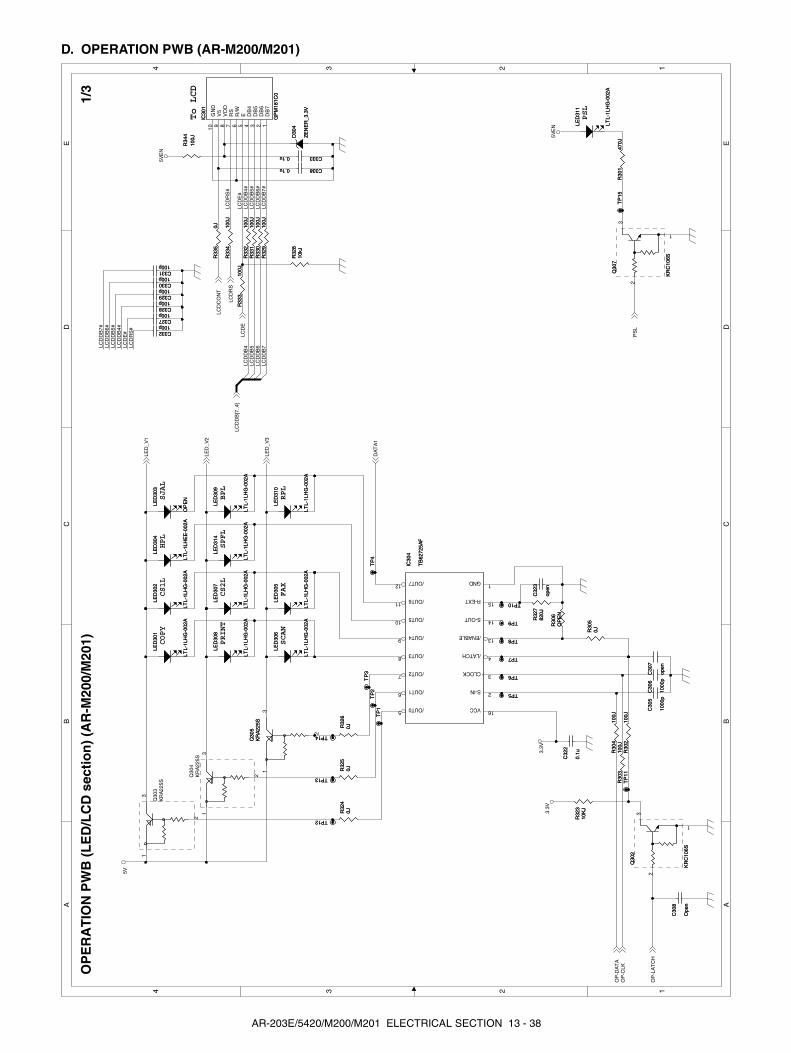
D. OPERATION PWB (AR-M200/M201)
LCD
RS
#
LCD
DB
7#
LCD
DB
4#
LCD
DB
6#
LCD
RS
#
LCD
E#
LCD
E#
LCD
DB
7#
LCD
DB
4#
LCD
DB
6#
LCD
DB
5#LC
DD
B6
LCD
DB
7
LCD
DB
4LCD
DB
5#
LCD
DB
5
5VE
N
5VE
N
3.3V
3.3V
5V
LED
_V2
OP
-CLK
OP
-DA
TA
OP
-LA
TC
H
LED
_V3
LED
_V1
DA
TA
1
LCD
E
LCD
RS
LCD
DB
[7..4
]
LCD
CO
NT
PS
L
To
LCD
FAX
SCAN
COPY
SPFL
HPL
SJAL
BPL
CS1L
CS2L
RPL
PSL
R33
310
0JR
333
100J
TP14 TP14
LTL-
1LH
G-0
02A
LED
308
LTL-
1LH
G-0
02A
LED
308
IC30
4
TB
6272
5AF
IC30
4
TB
6272
5AF
/OUT27
/OUT38
/OUT49
/OUT510
/OUT611
/OUT16
/OUT05 VCC 16
/ENABLE 13
/LATCH 4
S-IN 2
CLOCK 3
S-OUT 14
GND 1/OUT712
R-EXT 15
TP
1T
P1
LTL-
1LH
G-0
02A
LED
309
LTL-
1LH
G-0
02A
LED
309
C32
3
open
C32
3
open
Q30
7
KR
C10
6S
Q30
7
KR
C10
6S
1
2
3
TP
3T
P3
TP5 TP5
R30
210
0JR
302
100J
C329100pC329100p
R30
50JR
305
0J
R34
410
0JR
344
100J
LTL-
1LH
G-0
02A
LED
311
LTL-
1LH
G-0
02A
LED
311
TP
15T
P15
TP6 TP6
C330100pC330100p
LTL-
1LH
G-0
02A
LED
301
LTL-
1LH
G-0
02A
LED
301
R33
210
0JR
332
100J
LTL-
1LH
G-0
02A
LED
306
LTL-
1LH
G-0
02A
LED
306
TP
2T
P2
R33
50J
R33
50J
C332100pC332100p
R32
50JR
325
0J
R30
410
0JR
304
100J
R30
147
0JR
301
470J
C32
2
0.1u
C32
2
0.1u
LTL-
1LH
G-0
02A
LED
310
LTL-
1LH
G-0
02A
LED
310
R32
310
KJ
R32
310
KJ
C30
6
1000
p
C30
6
1000
p
OP
EN
LED
303
OP
EN
LED
303
R33
110
0JR
331
100J
TP10 TP10
LTL-
1LH
G-0
02A
LED
302
LTL-
1LH
G-0
02A
LED
302
IC30
1
GP
M18
1C0
IC30
1
GP
M18
1C0
GN
D1
0
V5
9
VD
D8
RS
7
R/W
6
E5
DB
44
DB
53
DB
62
DB
71
R32
782
0JR
327
820J
C3330.1u C3330.1u
Q30
5K
RA
225S
Q30
5K
RA
225S
3
2
1
TP9 TP9
LTL-
1LH
G-0
02A
LED
307
LTL-
1LH
G-0
02A
LED
307
Q30
3K
RA
225S
3
2
1
R30
6O
PE
NR
306
OP
EN
TP13 TP13
C331100pC331100p
R33
010
0JR
330
100J
Q30
4K
RA
225S
3
2
1
TP
11T
P11
LTL-
1LH
EE
-002
A
LED
304
LTL-
1LH
EE
-002
A
LED
304
LTL-
1LH
G-0
02A
LED
305
LTL-
1LH
G-0
02A
LED
305
TP8 TP8
TP
4T
P4
R33
410
0JR
334
100J
R32
40JR
324
0J
C30
5
1000
p
C30
5
1000
p
C327100pC327100p
R30
310
0JR
303
100J
LTL-
1LH
G-0
02A
LED
314
LTL-
1LH
G-0
02A
LED
314
C30
8
Ope
n
C30
8
Ope
n
Q30
2
KR
C10
6S
Q30
2
KR
C10
6S
1
2
3
D30
4
ZE
NE
R_3
.3V
D30
4
ZE
NE
R_3
.3V
R32
910
0JR
329
100J
C30
7
open
C30
7
open
R32
810
kJR
328
10kJ
C328100pC328100p
TP12 TP12
C3380.1u C3380.1u
TP7 TP7
R32
60JR
326
0J
A A
B B
C C
D D
E E
44
33
22
11
OP
ER
AT
ION
PW
B(L
ED
/LC
Dse
ctio
n)
(AR
-M20
0/M
201)
1/3
AR-203E/5420/M200/M201 ELECTRICAL SECTION 13 - 38

5V
5V
5VE
N
5V
KE
YS
C1
KE
YS
C2
KE
YS
C3
KE
YIN
SE
LIN
3S
ELI
N2
SE
LIN
1
PS
W
F-K
EY
SC
2F
-KE
YS
C3
F-K
EY
SC
1
F-K
EY
IN1
F-K
EY
IN2
F-K
EY
IN3
F-K
EY
IN4
F-K
EY
IN5
F-K
EY
IN6
F-K
EY
IN7
BZ
R
CAK
NM6K
NM1K
NM8K
RAT
ENT
LK
MODK
BPK
MENU
RK
NM7K
SHPK
NM4K
NM2K
CLK
NM3K
NM5K
NM9K
NM0K
ASTK
EXP
ESRT
2SIDE
PSW
R31
210
0JR
312
100J
R34
3
2kJ
R34
3
2kJ
KE
Y31
5
SK
QN
AB
D01
0
KE
Y31
5
SK
QN
AB
D01
0
TP
26T
P26
R31
71k
J
KE
Y30
6
SK
QN
AB
D01
0
KE
Y30
6
SK
QN
AB
D01
0
R33
910
kJR
339
10kJ
KE
Y32
1
SK
QN
AB
D01
0
KE
Y32
1
SK
QN
AB
D01
0
C31
7
Ope
n
C31
7
Ope
n
R30
710
0JR
307
100J
C30
9
Ope
n
TP
36T
P36
C31
9
Ope
n
TP
29T
P29
R31
310
0JR
313
100J
TP
24T
P24
TP
17T
P17
BZ
301
PS
1720
P02
BZ
301
PS
1720
P02
1
2
C33
4
Ope
n
C33
4
Ope
n
KE
Y32
5
SK
QN
AB
D01
0
KE
Y32
5
SK
QN
AB
D01
0
R30
910
0JR
309
100J
KE
Y30
7
SK
QN
AB
D01
0
KE
Y30
7
SK
QN
AB
D01
0
C31
0
Ope
nC31
8
Ope
n
TP
25T
P25
TP
33T
P33
KE
Y32
2
SK
QN
AB
D01
0
KE
Y32
2
SK
QN
AB
D01
0
KE
Y31
3
SK
QN
AB
D01
0
KE
Y31
3
SK
QN
AB
D01
0
TP
19T
P19
KE
Y30
2
SK
QN
AB
D01
0
KE
Y30
2
SK
QN
AB
D01
0
D30
2
1SS
133
D30
2
1SS
133
R31
833
JR
318
33J
R33
81k
J
C31
1
Ope
n
KE
Y32
4
SK
QN
AB
D01
0
KE
Y32
4
SK
QN
AB
D01
0
C31
6
Ope
n
C31
6
Ope
n
TP
21T
P21
R32
1
2kJ
R32
1
2kJ
KE
Y31
9
SK
QN
AB
D01
0
KE
Y31
9
SK
QN
AB
D01
0
TP
35T
P35
TP
28T
P28
R33
61k
J
R34
0
2kJ
R34
0
2kJ
KE
Y32
0
SK
QN
AB
D01
0
KE
Y32
0
SK
QN
AB
D01
0
KE
Y32
3
SK
QN
AB
D01
0
KE
Y32
3
SK
QN
AB
D01
0D
303
1SS
133
D30
3
1SS
133
R31
51k
J
R30
810
0JR
308
100J
KE
Y30
8
SK
QN
AB
D01
0
KE
Y30
8
SK
QN
AB
D01
0
R31
110
0JR
311
100J
C32
0
Ope
n
KE
Y31
8
SK
QN
AB
D01
0
KE
Y31
8
SK
QN
AB
D01
0
KE
Y31
2
SK
QN
AB
D01
0
KE
Y31
2
SK
QN
AB
D01
0
KE
Y30
1
SK
QN
AB
D01
0
KE
Y30
1
SK
QN
AB
D01
0
TP
31T
P31
TP
32T
P32
KE
Y31
0
SK
QN
AB
D01
0
KE
Y31
0
SK
QN
AB
D01
0
D30
1
1SS
133
D30
1
1SS
133
TP
23T
P23
R34
2
2kJ
R34
2
2kJ
KE
Y30
3
SK
QN
AB
D01
0
KE
Y30
3
SK
QN
AB
D01
0
C33
5
Ope
n
C33
5
Ope
n
R32
0
2kJ
R32
0
2kJ
R32
2
2kJ
R32
2
2kJ
KE
Y31
4
SK
QN
AB
D01
0
KE
Y31
4
SK
QN
AB
D01
0
IC30
2
74H
C15
1
IC30
2
74H
C15
1
D0
4
D1
3
D2
2
D3
1
D4
15
D5
14
D6
13
D7
12
A1
1
B1
0
C9
G7
W6
Y5
VC
C1
6
GN
D8
KE
Y31
7
SK
QN
AB
D01
0
KE
Y31
7
SK
QN
AB
D01
0
R31
9
2kJ
R31
9
2kJ
C33
6
Ope
n
C33
6
Ope
n
TP
16T
P16
TP
34T
P34
C32
1
0.1u
TP
27T
P27
R3482kJ
C30
4
Ope
n
C30
4
Ope
n
TP
18T
P18
KE
Y31
1
SK
QN
AB
D01
0
KE
Y31
1
SK
QN
AB
D01
0
R31
61k
J
R33
71k
J
TP
20T
P20
R31
410
0JR
314
100J
R3472kJ
Q30
6
KR
C10
6S
Q30
6
KR
C10
6S1
2
3
C31
3
Ope
n
C31
3
Ope
n
C31
5
47pF
TP
30T
P30
R34
1
2kJ
R34
1
2kJ
KE
Y30
9
SK
QN
AB
D01
0
KE
Y30
9
SK
QN
AB
D01
0
R3462kJ
KE
Y30
5
SK
QN
AB
D01
0
KE
Y30
5
SK
QN
AB
D01
0
C33
7
Ope
n
C33
7
Ope
n
KE
Y31
6
SK
QN
AB
D01
0
KE
Y31
6
SK
QN
AB
D01
0
R31
010
0JR
310
100J
IC30
3
74H
C23
8
IC30
3
74H
C23
8
GN
D8
Y0
15
Y1
14
Y2
13
Y3
12
Y4
11
Y5
10
Y6
9
Y7
7
A1
B2
C3
G2
B5
G2
A4
G1
6
VC
C1
6
TP
22T
P22
C31
4
Ope
n
C31
4
Ope
n
KE
Y30
4
SK
QN
AB
D01
0
KE
Y30
4
SK
QN
AB
D01
0
C31
2
0.1u
C31
2
0.1u
A A
B B
C C
D D
E E
44
33
22
11
OP
ER
AT
ION
PW
B(K
EY
/Bu
zzer
sect
ion
)(A
R-M
200/
M20
1)2/
3
AR-203E/5420/M200/M201 ELECTRICAL SECTION 13 - 39
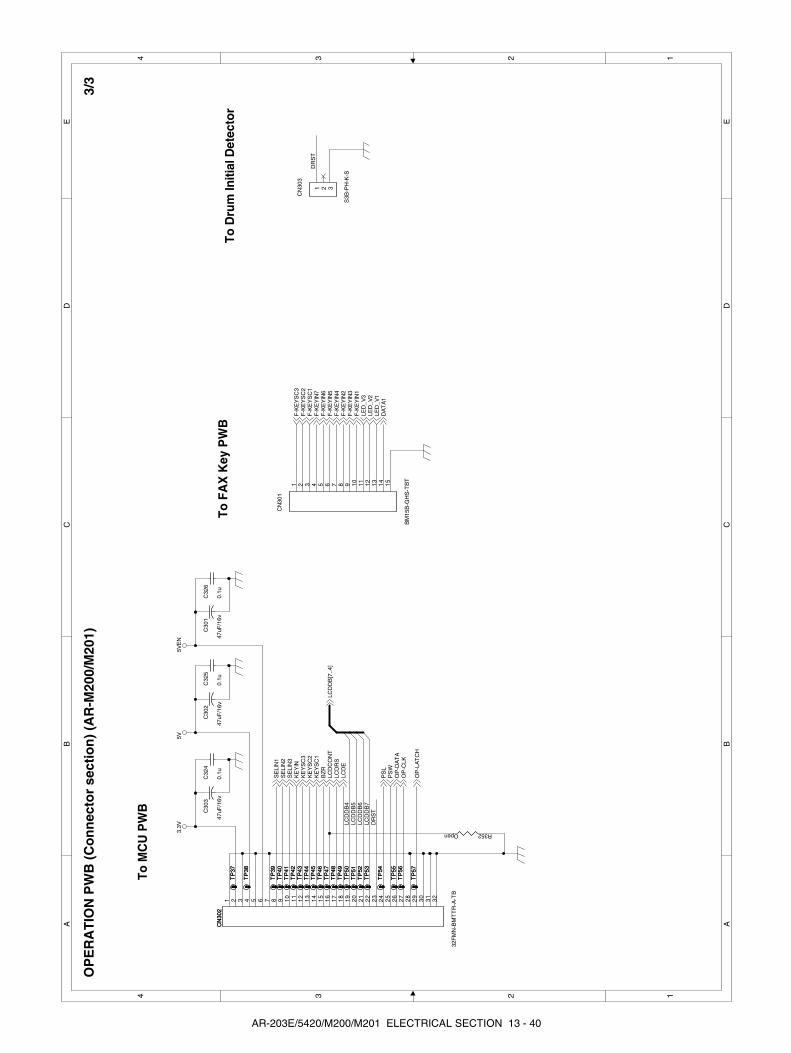
DR
ST
DR
ST
LCD
DB
5
LCD
DB
7
LCD
DB
4
LCD
DB
6
3.3V
5V5V
EN
PS
LP
SW
KE
YIN
OP
-CLK
OP
-LA
TC
H
OP
-DA
TA
SE
LIN
1S
ELI
N2
KE
YS
C2
KE
YS
C3
LED
_V3
F-K
EY
IN1
BZ
RK
EY
SC
1
LCD
RS
LCD
E
SE
LIN
3
LCD
DB
[7..4
]F
-KE
YIN
4
DA
TA
1
F-K
EY
IN2
LED
_V2
F-K
EY
IN5
LED
_V1
F-K
EY
SC
2
F-K
EY
IN6
F-K
EY
SC
3
F-K
EY
SC
1F
-KE
YIN
7
F-K
EY
IN3
LCD
CO
NT
ToM
CU
PW
B
ToD
rum
Initi
alD
etec
tor
ToFA
XK
eyP
WB
TP
43T
P43
TP
51T
P51
C30
3
47uF
/16v
TP
42T
P42
C32
6
0.1u
TP
50T
P50
TP
41T
P41
TP
49T
P49
CN
301
BM
15B
-GH
S-T
BT
1 2 3 4 5 6 7 8 9 10
11
12
13
14
15
TP
57T
P57
CN
302
32F
MN
-BM
TT
R-A
-TB
CN
302
1 2 3 4 5 6 7 8 9 10
11
12
13
14
15
16
17
18
19
20
21
22
23
24
25
26
27
28
29
30
31
32
R352Open
TP
48T
P48
C30
2
47uF
/16v
TP
56T
P56
TP
40T
P40
TP
52T
P52
TP
39T
P39
TP
54T
P54
TP
47T
P47
TP
55T
P55
TP
38T
P38
C32
4
0.1u
TP
46T
P46
TP
53T
P53
TP
37T
P37
TP
45T
P45
TP
44T
P44
C30
1
47uF
/16v
C32
5
0.1u
CN
303
S3B
-PH
-K-S
1 2 3
A A
B B
C C
D D
E E
44
33
22
11
OP
ER
AT
ION
PW
B(C
on
nec
tor
sect
ion
)(A
R-M
200/
M20
1)3/
3
AR-203E/5420/M200/M201 ELECTRICAL SECTION 13 - 40
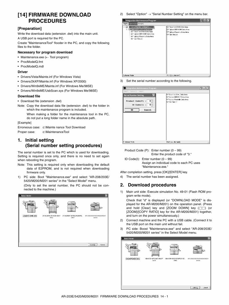
[14] FIRMWARE DOWNLOAD PROCEDURES
[Preparation]Write the download data (extension .dwl) into the main unit.
A USB port is required for the PC.
Create "MaintenanceTool" flooder in the PC, and copy the followingfiles to the folder.
Necessary for program download• Maintenance.exe (← Tool program)
• ProcModelQ.fmt
• ProcModelQ.mdl
Driver• Drivers/Vista/Mainte.inf (For Windows Vista)
• Drivers/2kXP/Mainte.inf (For Windows XP/2000)
• Drivers/Win9xME/Mainte.inf (For Windows Me/98SE)
• Drivers/Win9xME/UsbScan.sys (For Windows Me/98SE)
Download file• Download file (extension .dwl)
Note: Copy the download data file (extension .dwl) to the folder inwhich the maintenance program is included.
When making a folder for the maintenance tool in the PC,do not put a long folder name in the absolute path.
[Example]
Erroneous case: c:\Mainte nance Tool Download
Proper case: c:\MaintenanceTool
1. Initial setting (Serial number setting procedures)
The serial number is set to the PC which is used for downloading.Setting is required once only, and there is no need to set againwhen rebooting the program.
Note: This setting is required only when downloading the defaultdata of E2PROM, and is not required when downloadingfirmware only.
1) PC side: Boot "Maintenance.exe" and select "AR-208/203E/5420/M200/M201 series" in the "Select Model" menu.
(Only to set the serial number, the PC should not be con-nected to the machine.)
2) Select "Option" → "Serial Number Setting" on the menu bar.
3) Set the serial number according to the following.
After completion setting, press [OK]/[ENTER] key.
4) The serial number has been assigned.
2. Download procedures1) Main unit side: Execute simulation No. 49-01 (Flash ROM pro-
gram write mode).
Check that "d" is displayed (or "DOWNLOAD MODE" is dis-played for the AR-M200/M201) on the operation panel. (Pressand hold [Clear] key and [ZOOM DOWN] key ( ) (or[ZOOM]/[COPY RATIO] key for the AR-M200/M201) together,and turn on the power simultaneously.)
2) Connect machine and the PC with a USB cable. (Connect it tothe USB port on the main unit without fail.
3) PC side: Boost "Maintenance.exe" and select "AR-208/203E/5420/M200/M201 series" in the Select Model menu.
AR-208/203E/5420/M200/M201
series
Product Code (P): Enter number (0 – 99)Enter the product code of "3."
ID Code(I): Enter number (0 – 99)Assign an individual code to each PC uses"Maintenance.exe."
AR-208/203E/5420/M200/M201
series
AR-203E/5420/M200/M201 FIRMWARE DOWNLOAD PROCEDURES 14 - 1

4) PC side: Check that the "Simulation Command List" tree is dis-played on the integration maintenance program.
5) PC side: When the integration maintenance program isboosted and "The copier is not turned on." is displayed at thebottom of display, select "File" → "Reconnect" on the menubar.
6) PC side: Check that trees are displayed in the "Special (MCU/IMC2/Facsimile)" folder in the integration maintenance pro-gram. (If trees are not displayed, check that the USB connec-tor is connected, and select "Reconnect" in procedure 5)again.)
7) PC side: Double-click "Special (MCU/IMC2/Facsimile)" in themain tree to develop its sub trees, and double-click "DownloadDWL Data Area" in the sub trees.
8) PC side: Specify the download file (*****.dwl) to be used.
9) PC side: When a download file is specified, downloading isperformed automatically.
10) PC side: When download is completed, the following mes-sage is displayed.
Note: Since, however, the machine enters the download datawrite state, do not turn OFF the power of the machine at thismoment.
11) Main unit side: Wait until "0FF" is displayed (or "DOWNLOADCOMPLETE!" is displayed for the AR-M200/M201) on theoperation panel. When "0FF" is displayed (or "DOWNLOADCOMPLETE!" is displayed for the AR-M200/M201), downloadis completed.
Turn OFF the power of the machine, and disconnect the USBcable.
12) Terminate the integration maintenance program, and turn ONthe machine again.
Download is completed with the above procedures.
AR-203E/5420/M200/M201 FIRMWARE DOWNLOAD PROCEDURES 14 - 2

Note: When another machine is connected, connect the USBcable again and select "File" → "Reconnect" on the menubar of the integration maintenance program. Repeat theabove procedures from 5).
* Inhibition during download (Important)If download is failed, the next download may not be executed. Usegreat care not to execute the following items during download.
• Never turn off the machine.
• Never disconnect the download cable (USB cable).
* If the above inhibition item occurs during downloading, turn OFF/ON the power.
1) When "d" is displayed (or "DOWNLOAD MODE" is displayedfor the AR-M200/M201) on the operation panel, execute thedownload procedure again.
2) If "d" is not displayed (or "DOWNLOAD MODE" is not displayedfor the AR-M200/M201) on the operation panel, turn OFF thepower and press and hold [Clear] key and [ZOOM DOWN] key( ) (or [ZOOM]/[COPY RATIO] key for the AR-M200/M201)and turn ON the power. Check that "d" is displayed (or"DOWNLOAD MODE" is displayed for the AR-M200/M201) onthe operation panel, and execute the download procedureagain.
If "d" is not still displayed (or "DOWNLOAD MODE" is not stilldisplayed for the AR-M200/M201), replace the MCU with a newone.
3. Version acquisition procedures1) Main unit side: Execute simulation No. 49-01 (Flash ROM pro-
gram write mode).
Check that "d" is displayed (or "DOWNLOAD MODE" is dis-played for the AR-M200/M201) on the operation panel of themain unit. (Press and hold [Clear] key and [ZOOM DOWN] key( ) (or [ZOOM]/[COPY RATIO] key for the AR-M200/M201)together, and turn on the power simultaneously.)
2) Connect the machine and the PC with a USB cable.
3) PC side: Boost "Maintenance.exe" and select "AR-208/203E/5420/M200/M201 series" in the "Select Model" menu.
4) PC side: Check that the "Simulation Command List" tree onthe integration maintenance program.
5) PC side: Boot the integration maintenance program. If "Thecopier is not turned on." is displayed, select "File" → "Recon-nect" on the menu bar.
6) PC side: Check that trees are displayed on "Special (MCU/IMC2/Facsimile" in the integration maintenance program. (Iftrees are not displayed, check that the USB cable is connectedand select "Reconnect" again in procedure 5).
AR-208/203E/5420/M200/M201
series
AR-203E/5420/M200/M201 FIRMWARE DOWNLOAD PROCEDURES 14 - 3
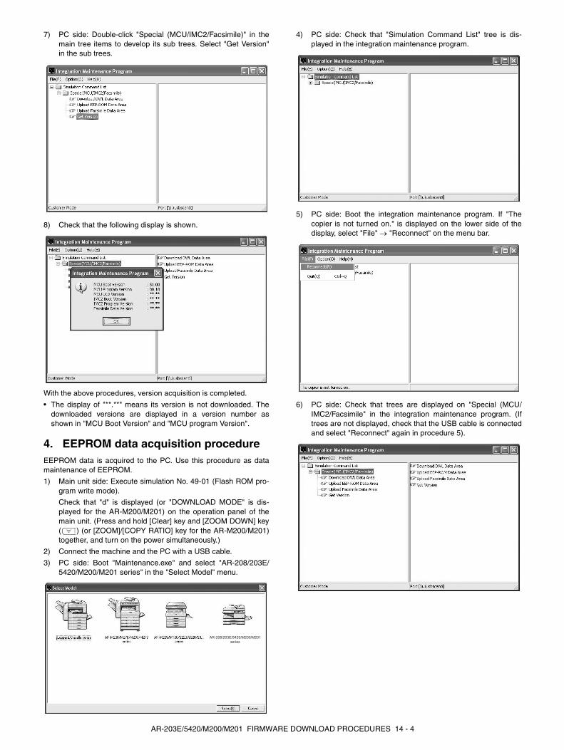
7) PC side: Double-click "Special (MCU/IMC2/Facsimile)" in themain tree items to develop its sub trees. Select "Get Version"in the sub trees.
8) Check that the following display is shown.
With the above procedures, version acquisition is completed.
• The display of "**.**" means its version is not downloaded. Thedownloaded versions are displayed in a version number asshown in "MCU Boot Version" and "MCU program Version".
4. EEPROM data acquisition procedureEEPROM data is acquired to the PC. Use this procedure as datamaintenance of EEPROM.
1) Main unit side: Execute simulation No. 49-01 (Flash ROM pro-gram write mode).
Check that "d" is displayed (or "DOWNLOAD MODE" is dis-played for the AR-M200/M201) on the operation panel of themain unit. (Press and hold [Clear] key and [ZOOM DOWN] key( ) (or [ZOOM]/[COPY RATIO] key for the AR-M200/M201)together, and turn on the power simultaneously.)
2) Connect the machine and the PC with a USB cable.
3) PC side: Boot "Maintenance.exe" and select "AR-208/203E/5420/M200/M201 series" in the "Select Model" menu.
4) PC side: Check that "Simulation Command List" tree is dis-played in the integration maintenance program.
5) PC side: Boot the integration maintenance program. If "Thecopier is not turned on." is displayed on the lower side of thedisplay, select "File" → "Reconnect" on the menu bar.
6) PC side: Check that trees are displayed on "Special (MCU/IMC2/Facsimile" in the integration maintenance program. (Iftrees are not displayed, check that the USB cable is connectedand select "Reconnect" again in procedure 5).
AR-208/203E/5420/M200/M201
series
AR-203E/5420/M200/M201 FIRMWARE DOWNLOAD PROCEDURES 14 - 4
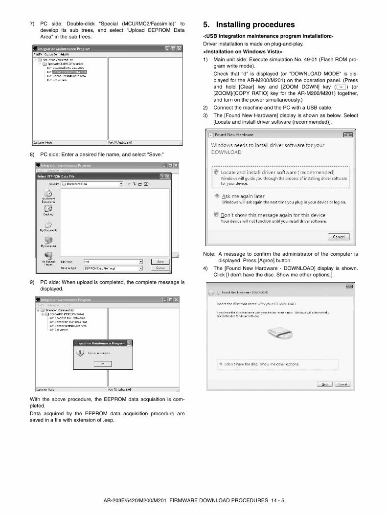
7) PC side: Double-click "Special (MCU/IMC2/Facsimile)" todevelop its sub trees, and select "Upload EEPROM DataArea" in the sub trees.
8) PC side: Enter a desired file name, and select "Save."
9) PC side: When upload is completed, the complete message isdisplayed.
With the above procedure, the EEPROM data acquisition is com-pleted.
Data acquired by the EEPROM data acquisition procedure aresaved in a file with extension of .eep.
5. Installing procedures<USB integration maintenance program installation>
Driver installation is made on plug-and-play.
<Installation on Windows Vista>
1) Main unit side: Execute simulation No. 49-01 (Flash ROM pro-gram write mode).
Check that "d" is displayed (or "DOWNLOAD MODE" is dis-played for the AR-M200/M201) on the operation panel. (Pressand hold [Clear] key and [ZOOM DOWN] key ( ) (or[ZOOM]/[COPY RATIO] key for the AR-M200/M201) together,and turn on the power simultaneously.)
2) Connect the machine and the PC with a USB cable.
3) The [Found New Hardware] display is shown as below. Select[Locate and install driver software (recommended)].
Note: A message to confirm the administrator of the computer isdisplayed. Press [Agree] button.
4) The [Found New Hardware - DOWNLOAD] display is shown.Click [I don't have the disc. Show me other options.].
AR-203E/5420/M200/M201 FIRMWARE DOWNLOAD PROCEDURES 14 - 5

5) When the following display is shown, select [Browse my com-puter for driver software (advanced)].
6) The following display is shown.
7) Press [Browse] button, specify the folder which includes themaintenance tool driver (Maintenance.inf), and press [OK] but-ton.
8) The path to the folder which includes the maintenance tooldriver (Maintenance.inf) is displayed. Press [Next] button.
9) When the following display is shown, select [Install this driversoftware anyway].
10) When the following display is shown, close [Close] button tocomplete installation.
AR-203E/5420/M200/M201 FIRMWARE DOWNLOAD PROCEDURES 14 - 6

<Installation on Windows XP>
1) Main unit side: Execute simulation No. 49-01 (Flash ROM pro-gram write mode).
Check that "d" is displayed (or "DOWNLOAD MODE" is dis-played for the AR-M200/M201) on the operation panel. (Pressand hold [Clear] key and [ZOOM DOWN] key ( ) (or[ZOOM]/[COPY RATIO] key for the AR-M200/M201) together,and turn on the power simultaneously.)
2) Connect the machine and the PC with a USB cable.
3) The following display is shown.
Select [Install from a list or specific location] and press <Next>button.
4) Select [Include this location in the search;]. If the search loca-tion is not the folder which includes the maintenance tooldriver (Mainte.inf), select <Browse>. If the search location isthe folder which includes the maintenance tool driver, press<Next> button to go to procedure 7).
5) Select the folder which includes the maintenance tool driver(Mainte.inf) and press <OK> button.
(Suppose that the driver is included in C:\MaintenanceTool\Drivers\2kXp folder.)
6) Check the path to the folder which includes the maintenancetool driver (Mainte.inf), and press <Next> button.
7) When the following display is shown, press [Continue Anyway]button.
AR-203E/5420/M200/M201 FIRMWARE DOWNLOAD PROCEDURES 14 - 7

8) When the following display is shown, installation is completed.
Press <Finish> button.
With the above procedures, installation (on Windows XP) of theintegration maintenance program is completed.
<Installation on Windows 2000>
1) Main unit side: Execute simulation No. 49-01 (Flash ROM pro-gram write mode).
Check that "d" is displayed (or "DOWNLOAD MODE" is dis-played for the AR-M200/M201) on the operation panel. (Pressand hold [Clear] key and [ZOOM DOWN] key ( ) (or[ZOOM]/[COPY RATIO] key for the AR-M200/M201) together,and turn on the power simultaneously.)
2) Connect the machine and the PC with a USB cable.
3) Check that the Found New Hardware Wizard is displayed, andpress <Next> button.
4) Select [Search for a suitable driver for my device] and press<Next> button.
5) Select [Specify a location] and press <Next> button.
6) Select [Include this location in the search;]. If the search loca-tion is not the folder which includes the maintenance tool driver(Mainte.inf), select <Browse>. If the search location is thefolder which includes the maintenance tool driver, press<Next> button to go to procedure 9).
7) Specify the folder which includes the maintenance tool driver(Mainte.inf), and press <Open> button.
AR-203E/5420/M200/M201 FIRMWARE DOWNLOAD PROCEDURES 14 - 8
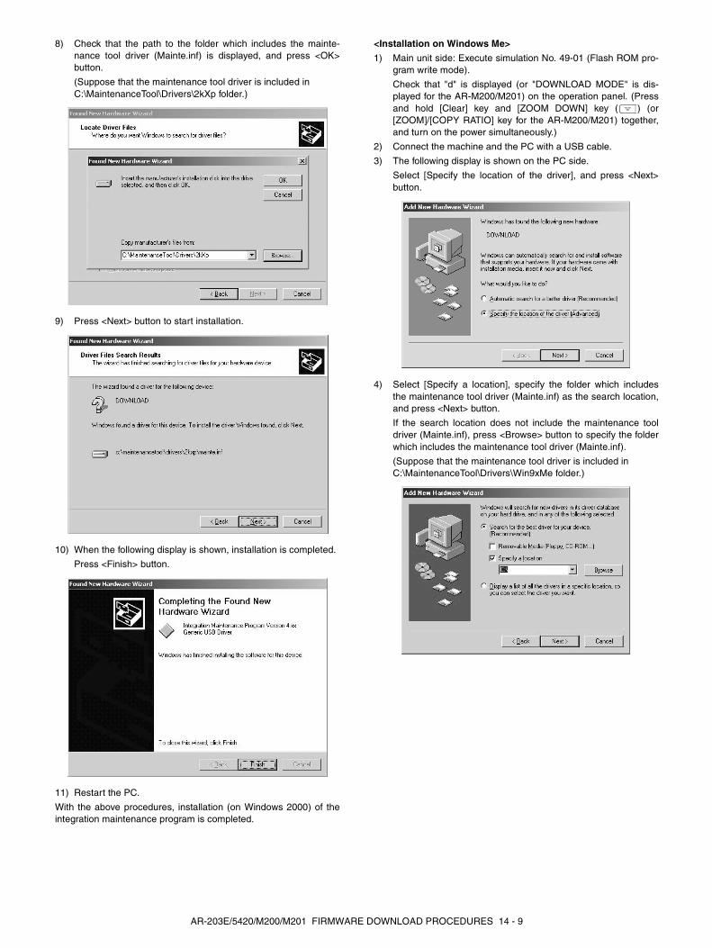
8) Check that the path to the folder which includes the mainte-nance tool driver (Mainte.inf) is displayed, and press <OK>button.
(Suppose that the maintenance tool driver is included in C:\MaintenanceTool\Drivers\2kXp folder.)
9) Press <Next> button to start installation.
10) When the following display is shown, installation is completed.
Press <Finish> button.
11) Restart the PC.
With the above procedures, installation (on Windows 2000) of theintegration maintenance program is completed.
<Installation on Windows Me>
1) Main unit side: Execute simulation No. 49-01 (Flash ROM pro-gram write mode).
Check that "d" is displayed (or "DOWNLOAD MODE" is dis-played for the AR-M200/M201) on the operation panel. (Pressand hold [Clear] key and [ZOOM DOWN] key ( ) (or[ZOOM]/[COPY RATIO] key for the AR-M200/M201) together,and turn on the power simultaneously.)
2) Connect the machine and the PC with a USB cable.
3) The following display is shown on the PC side.
Select [Specify the location of the driver], and press <Next>button.
4) Select [Specify a location], specify the folder which includesthe maintenance tool driver (Mainte.inf) as the search location,and press <Next> button.
If the search location does not include the maintenance tooldriver (Mainte.inf), press <Browse> button to specify the folderwhich includes the maintenance tool driver (Mainte.inf).
(Suppose that the maintenance tool driver is included in C:\MaintenanceTool\Drivers\Win9xMe folder.)
AR-203E/5420/M200/M201 FIRMWARE DOWNLOAD PROCEDURES 14 - 9
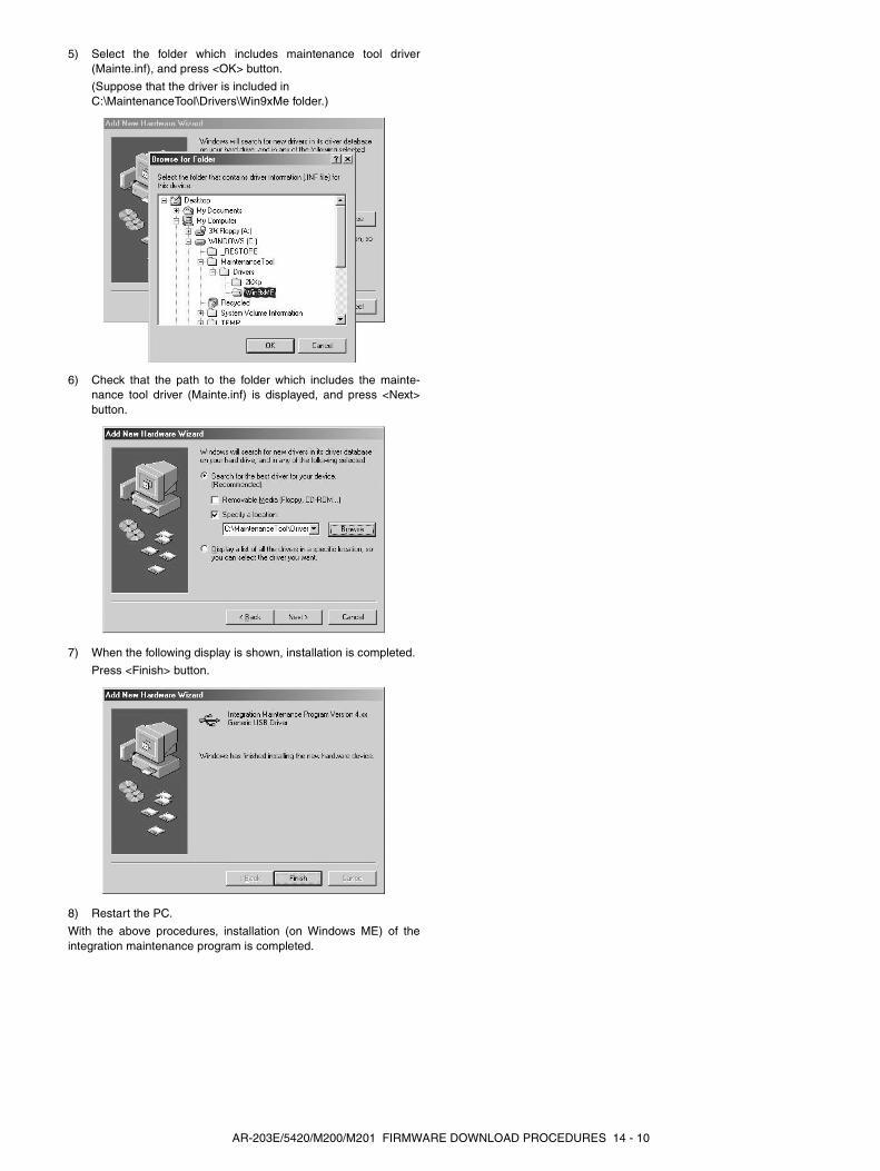
5) Select the folder which includes maintenance tool driver(Mainte.inf), and press <OK> button.
(Suppose that the driver is included in C:\MaintenanceTool\Drivers\Win9xMe folder.)
6) Check that the path to the folder which includes the mainte-nance tool driver (Mainte.inf) is displayed, and press <Next>button.
7) When the following display is shown, installation is completed.
Press <Finish> button.
8) Restart the PC.
With the above procedures, installation (on Windows ME) of theintegration maintenance program is completed.
AR-203E/5420/M200/M201 FIRMWARE DOWNLOAD PROCEDURES 14 - 10

Memo

Memo

LEAD-FREE SOLDER
The PWB’s of this model employs lead-free solder. The “LF” marks indicated on the PWB’s and the Service Manual mean “Lead-Free” solder.
The alphabet following the LF mark shows the kind of lead-free solder.
(1) NOTE FOR THE USE OF LEAD-FREE SOLDER THREAD
When repairing a lead-free solder PWB, use lead-free solder thread.
Never use conventional lead solder thread, which may cause a breakdown or an accident.
Since the melting point of lead-free solder thread is about 40°C higher than that of conventional lead solder thread, the use of the exclusive-usesoldering iron is recommendable.
(2) NOTE FOR SOLDERING WORK
Since the melting point of lead-free solder is about 220°C, which is about 40°C higher than that of conventional lead solder, and its soldering capacity isinferior to conventional one, it is apt to keep the soldering iron in contact with the PWB for longer time. This may cause land separation or may exceedthe heat-resistive temperature of components. Use enough care to separate the soldering iron from the PWB when completion of soldering isconfirmed.
Since lead-free solder includes a greater quantity of tin, the iron tip may corrode easily. Turn ON/OFF the soldering iron power frequently.
If different-kind solder remains on the soldering iron tip, it is melted together with lead-free solder. To avoid this, clean the soldering iron tip aftercompletion of soldering work.
If the soldering iron tip is discolored black during soldering work, clean and file the tip with steel wool or a fine filer.
Example:
5mm
Lead-Free
Solder compositioncode (Refer to thetable at the right.)
<Solder composition code of lead-free solder>
Solder composition
Sn-Ag-Cu
Sn-Ag-BiSn-Ag-Bi-Cu
Sn-Zn-Bi
Sn-In-Ag-Bi
Sn-Cu-Ni
Sn-Ag-Sb
Bi-Sn-Ag-PBi-Sn-Ag
a
b
z
i
n
s
p
Solder composition code
a
CAUTION FOR BATTERY REPLACEMENT
(Danish) ADVARSEL !Lithiumbatteri – Eksplosionsfare ved fejlagtig håndtering.
Udskiftning må kun ske med batteriaf samme fabrikat og type.
Levér det brugte batteri tilbage til leverandoren.
(English) Caution !Danger of explosion if battery is incorrectly replaced.
Replace only with the same or equivalent typerecommended by the manufacturer.
Dispose of used batteries according to manufacturer’s instructions.
(Finnish) VAROITUSParisto voi räjähtää, jos se on virheellisesti asennettu.
Vaihda paristo ainoastaan laitevalmistajan suosittelemaantyyppiin. Hävitä käytetty paristo valmistajan ohjeiden
mukaisesti.
(French) ATTENTIONIl y a danger d’explosion s’ il y a remplacement incorrect
de la batterie. Remplacer uniquement avec une batterie dumême type ou d’un type équivalent recommandé par
le constructeur.Mettre au rebut les batteries usagées conformément aux
instructions du fabricant.
(Swedish) VARNINGExplosionsfara vid felaktigt batteribyte.
Använd samma batterityp eller en ekvivalenttyp som rekommenderas av apparattillverkaren.
Kassera använt batteri enligt fabrikantensinstruktion.
(German) AchtungExplosionsgefahr bei Verwendung inkorrekter Batterien.
Als Ersatzbatterien dürfen nur Batterien vom gleichen Typ odervom Hersteller empfohlene Batterien verwendet werden.Entsorgung der gebrauchten Batterien nur nach den vom
Hersteller angegebenen Anweisungen.
CAUTION FOR BATTERY DISPOSAL
(For USA, CANADA)"BATTERY DISPOSAL"
THIS PRODUCT CONTAINS A LITHIUM PRIMARY(MANGANESS DIOXIDE) MEMORY BACK-UP BATTERY
THAT MUST BE DISPOSED OF PROPERLY. REMOVE THEBATTERY FROM THE PRODUCT AND CONTACT YOUR
LOCAL ENVIRONMENTAL AGENCIES FOR INFORMATIONON RECYCLING AND DISPOSAL OPTIONS.
"TRAITEMENT DES PILES USAGÉES"CE PRODUIT CONTIENT UNE PILE DE SAUVEGARDE DE
MÉMOIRE LITHIUM PRIMAIRE (DIOXYDE DE MANGANÈSE)QUI DOIT ÊTRE TRAITÉE CORRECTEMENT. ENLEVEZ LAPILE DU PRODUIT ET PRENEZ CONTACT AVEC VOTRE
AGENCE ENVIRONNEMENTALE LOCALE POUR DESINFORMATIONS SUR LES MÉTHODES DE RECYCLAGE ET
DE TRAITEMENT.

COPYRIGHT © 2008 BY SHARP CORPORATIONAll rights reserved.Printed in Japan.
No part of this publication may be reproduced,stored in a retrieval system, or transmitted,
in any form or by any means,
electronic; mechanical; photocopying; recording or otherwisewithout prior written permission of the publisher.
Trademark acknowledgements• Microsoft®, Windows®, Windows® 98, Windows® Me, Windows® 2000,
Windows® XP, Windows® Vista, and Internet Explorer® are registered trademarks or trademarks of Microsoft Corporation in the U.S.A. and other countries.
• Adobe®, the Adobe® logo, Acrobat®, the Adobe® PDF logo, and ReaderTM are registered trademarks or trademarks of Adobe Systems Incorporated in the United States and other countries.
• IBM, PC/AT, and PowerPC are trademarks of International Business Machines Corporation.
• Sharpdesk is a trademark of Sharp Corporation.
• All other trademarks and copyrights are the property of their respective owners.
SHARP CORPORATIONDigital Document System GroupCS Promotion CenterYamatokoriyama, Nara 639-1186, Japan
2008 April Printed in Japan