Applied Surface Science - University of Surreyepubs.surrey.ac.uk/842027/7/Comparison of the surfaces...
14
Applied Surface Science 427 (2018) 1257–1270 Contents lists available at ScienceDirect Applied Surface Science journal homepage: www.elsevier.com/locate/apsusc Full Length Article Comparison of the surfaces and interfaces formed for sputter and electroless deposited gold contacts on CdZnTe Steven J. Bell a,b,c,∗,1 , Mark A. Baker b , Diana D. Duarte a,b , Andreas Schneider a , Paul Seller a , Paul J. Sellin b , Matthew C. Veale a , Matthew D. Wilson a a Rutherford Appleton Laboratory, Harwell-Oxford, Oxfordshire, OX11 0QX, UK b Faculty of Engineering and Physical Sciences, University of Surrey, Guildford, Surrey, GU2 7XH, UK c National Physical Laboratory, Hampton Road, Teddington, Middlesex, TW11 0LW, UK a r t i c l e i n f o Article history: Received 1 March 2017 Received in revised form 6 August 2017 Accepted 9 August 2017 Available online 12 August 2017 Keywords: CdZnTe Electroless deposition Metal-semiconductor interface Angle-resolved X-ray photoelectron spectroscopy Focused ion beam cross section imaging Current-voltage analysis a b s t r a c t Cadmium zinc telluride (CdZnTe) is a leading sensor material for spectroscopic X/-ray imaging in the fields of homeland security, medical imaging, industrial analysis and astrophysics. The metal- semiconductor interface formed during contact deposition is of fundamental importance to the spectroscopic performance of the detector and is primarily determined by the deposition method. A multi-technique analysis of the metal-semiconductor interface formed by sputter and electroless depo- sition of gold onto (111) aligned CdZnTe is presented. Focused ion beam (FIB) cross section imaging, X-ray photoelectron spectroscopy (XPS) depth profiling and current-voltage (IV) analysis have been applied to determine the structural, chemical and electronic properties of the gold contacts. In a novel approach, principal component analysis has been employed on the XPS depth profiles to extract detailed chemi- cal state information from different depths within the profile. It was found that electroless deposition forms a complicated, graded interface comprised of tellurium oxide, gold/gold telluride particulates, and cadmium chloride. This compared with a sharp transition from surface gold to bulk CdZnTe observed for the interface formed by sputter deposition. The electronic (IV) response for the detector with electroless deposited contacts was symmetric, but was asymmetric for the detector with sputtered gold contacts. This is due to the electroless deposition degrading the difference between the Cd- and Te-faces of the CdZnTe (111) crystal, whilst these differences are maintained for the sputter deposited gold contacts. This work represents an important step in the optimisation of the metal-semiconductor interface which currently is a limiting factor in the development of high resolution CdZnTe detectors. © 2017 The Authors. Published by Elsevier B.V. This is an open access article under the CC BY-NC-ND license (http://creativecommons.org/licenses/by-nc-nd/4.0/). 1. Introduction Cadmium telluride (CdTe) and cadmium zinc telluride (CdZnTe), collectively referred to as Cd(Zn)Te, are wide-bandgap semicon- ductors with high X/-ray stopping power. This combination of properties has led to Cd(Zn)Te being adopted in the fields of medical imaging, homeland security, industrial analysis and astrophysics as a compact, room temperature radiation detector/imager [1–5]. Metal contacts are required to measure a signal from the Cd(Zn)Te charge carriers generated by the incoming radiation. High ∗ Corresponding author at: National Physical Laboratory, Hampton Road, Tedding- ton, Middlesex, TW11 0LW, UK. E-mail address: [email protected] (S.J. Bell). 1 The author is now working at the National Physical Laboratory however the cur- rent work was performed at the Rutherford Appleton Laboratory and the University of Surrey. quality contacts have been successfully deposited on CdTe [6–8], but due to the low resistivity of CdTe (∼10 7–9 .cm) these con- tacts are typically Schottky in-nature to minimise leakage current. Schottky contacts can create instabilities in the electric field (polar- ization) due to the formation of space charge [9,10]. Increasing the detector bias improves stability however an increasingly large bias is required to achieve full charge collection and stability against polarization as the CdTe thickness increases. For CdTe thicker than 1 mm, the required bias is often large enough to induce electronic breakdown. This limits the practical thickness of Schottky CdTe detectors to 1 mm, which greatly reduces X/−ray detection effi- ciency for energies >100 keV. A 1 mm sensor cannot provide the detection efficiency required by applications such as SPECT (single photon emission computed tomography) or industrial component analysis which utilise higher X/−ray energies. The high resistivity of CdZnTe means Schottky contacts are not required and so CdZnTe detectors do not suffer the same bias-induced polarization effects http://dx.doi.org/10.1016/j.apsusc.2017.08.077 0169-4332/© 2017 The Authors. Published by Elsevier B.V. This is an open access article under the CC BY-NC-ND license (http://creativecommons.org/licenses/by-nc-nd/4. 0/).
Transcript of Applied Surface Science - University of Surreyepubs.surrey.ac.uk/842027/7/Comparison of the surfaces...

F
Ce
SPa
b
c
a
ARRAA
KCEMAsFC
1
cdpia
C
t
ro
h00
Applied Surface Science 427 (2018) 1257–1270
Contents lists available at ScienceDirect
Applied Surface Science
journa l homepage: www.e lsev ier .com/ locate /apsusc
ull Length Article
omparison of the surfaces and interfaces formed for sputter andlectroless deposited gold contacts on CdZnTe
teven J. Bell a,b,c,∗,1, Mark A. Baker b, Diana D. Duarte a,b, Andreas Schneider a,aul Seller a, Paul J. Sellin b, Matthew C. Veale a, Matthew D. Wilson a
Rutherford Appleton Laboratory, Harwell-Oxford, Oxfordshire, OX11 0QX, UKFaculty of Engineering and Physical Sciences, University of Surrey, Guildford, Surrey, GU2 7XH, UKNational Physical Laboratory, Hampton Road, Teddington, Middlesex, TW11 0LW, UK
r t i c l e i n f o
rticle history:eceived 1 March 2017eceived in revised form 6 August 2017ccepted 9 August 2017vailable online 12 August 2017
eywords:dZnTelectroless depositionetal-semiconductor interface
ngle-resolved X-ray photoelectronpectroscopyocused ion beam cross section imagingurrent-voltage analysis
a b s t r a c t
Cadmium zinc telluride (CdZnTe) is a leading sensor material for spectroscopic X/�-ray imaging inthe fields of homeland security, medical imaging, industrial analysis and astrophysics. The metal-semiconductor interface formed during contact deposition is of fundamental importance to thespectroscopic performance of the detector and is primarily determined by the deposition method. Amulti-technique analysis of the metal-semiconductor interface formed by sputter and electroless depo-sition of gold onto (111) aligned CdZnTe is presented. Focused ion beam (FIB) cross section imaging, X-rayphotoelectron spectroscopy (XPS) depth profiling and current-voltage (IV) analysis have been applied todetermine the structural, chemical and electronic properties of the gold contacts. In a novel approach,principal component analysis has been employed on the XPS depth profiles to extract detailed chemi-cal state information from different depths within the profile. It was found that electroless depositionforms a complicated, graded interface comprised of tellurium oxide, gold/gold telluride particulates, andcadmium chloride. This compared with a sharp transition from surface gold to bulk CdZnTe observed forthe interface formed by sputter deposition. The electronic (IV) response for the detector with electroless
deposited contacts was symmetric, but was asymmetric for the detector with sputtered gold contacts.This is due to the electroless deposition degrading the difference between the Cd- and Te-faces of theCdZnTe (111) crystal, whilst these differences are maintained for the sputter deposited gold contacts.This work represents an important step in the optimisation of the metal-semiconductor interface whichcurrently is a limiting factor in the development of high resolution CdZnTe detectors.© 2017 The Authors. Published by Elsevier B.V. This is an open access article under the CC BY-NC-ND
. Introduction
Cadmium telluride (CdTe) and cadmium zinc telluride (CdZnTe),ollectively referred to as Cd(Zn)Te, are wide-bandgap semicon-uctors with high X/�-ray stopping power. This combination ofroperties has led to Cd(Zn)Te being adopted in the fields of medical
maging, homeland security, industrial analysis and astrophysics as
compact, room temperature radiation detector/imager [1–5].Metal contacts are required to measure a signal from thed(Zn)Te charge carriers generated by the incoming radiation. High
∗ Corresponding author at: National Physical Laboratory, Hampton Road, Tedding-on, Middlesex, TW11 0LW, UK.
E-mail address: [email protected] (S.J. Bell).1 The author is now working at the National Physical Laboratory however the cur-
ent work was performed at the Rutherford Appleton Laboratory and the Universityf Surrey.
ttp://dx.doi.org/10.1016/j.apsusc.2017.08.077169-4332/© 2017 The Authors. Published by Elsevier B.V. This is an open access article
/).
license (http://creativecommons.org/licenses/by-nc-nd/4.0/).
quality contacts have been successfully deposited on CdTe [6–8],but due to the low resistivity of CdTe (∼107–9�.cm) these con-tacts are typically Schottky in-nature to minimise leakage current.Schottky contacts can create instabilities in the electric field (polar-ization) due to the formation of space charge [9,10]. Increasing thedetector bias improves stability however an increasingly large biasis required to achieve full charge collection and stability againstpolarization as the CdTe thickness increases. For CdTe thicker than1 mm, the required bias is often large enough to induce electronicbreakdown. This limits the practical thickness of Schottky CdTedetectors to 1 mm, which greatly reduces X/�−ray detection effi-ciency for energies >100 keV. A 1 mm sensor cannot provide thedetection efficiency required by applications such as SPECT (single
photon emission computed tomography) or industrial componentanalysis which utilise higher X/�−ray energies. The high resistivityof CdZnTe means Schottky contacts are not required and so CdZnTedetectors do not suffer the same bias-induced polarization effectsunder the CC BY-NC-ND license (http://creativecommons.org/licenses/by-nc-nd/4.

1 ce Scie
as
itCtebatitrsot[OwigbDais
(dCttafltsmtdrtbXsrthp
2
2
wwm3unau[
258 S.J. Bell et al. / Applied Surfa
s CdTe. Detectors with 15 mm thick CdZnTe sensors have beenuccessfully demonstrated [11].
Gold is used as a contact metal for CdZnTe as it does not oxidise,t’s highly conductive and has a work function of 5.1 eV [12], close tohat of high resistivity CdZnTe. Gold contacts may be deposited ontodZnTe by thermal evaporation, sputtering or electroless deposi-ion. Of these methods, it was decided to investigate sputter andlectroless deposition. Electroless deposition was chosen as it haseen reported to produce strong adhesion due to chemical bondingt the interface [13–15]. The adhesion of thermally evaporated con-acts has been reported to be inferior [13]. Good adhesion is vitalf the contacts are to survive pixellation and so thermal evapora-ion was not investigated in the current work. Further, it has beeneported that detectors with electroless gold contacts are betteruited for spectroscopic measurements compared with sputteredr thermally evaporated contacts [15–18]. Platinum is an alterna-ive choice of contact metal as it has a work function of 5.65 eV12], however electroless gold has been shown to produce a morehmic response [16,19] and better spectroscopy [15] comparedith electroless platinum. Micro-cracking has also been observed
n electroless platinum contacts but does not occur in electrolessold contacts [14]. This was attributed to a smaller lattice mismatchetween gold and CdZnTe compared with platinum and CdZnTe.espite the wealth of data available in the literature there is still
need for research on the subject of contacts on CdZnTe. Thiss because of the many possible combinations of material grade,urface preparation, choice of metal and method of deposition.
The Rutherford Appleton Laboratory (RAL) and the HEXITECHigh Energy X-ray Imaging Technology) collaboration [20] haveeveloped a family of spectroscopic small-pixel (250 �m pitch)dTe and CdZnTe detectors, based on the HEXITEC ASIC (applica-ion specific integrated circuit) [21–25]. The latest generation ofhe HEXITEC ASIC bonded to a CdTe sensor has achieved an aver-ge FWHM (full width at half maximum) energy resolution over theull 6400 pixels of the detector of 750 ± 60 eV at 59.54 keV [26]. Thisevel of performance has enabled cutting-edge imaging techniqueso be utilised in the fields of medical imaging [27–29], homelandecurity [30,31] and materials science [32–34]. As explained above,any of these applications would benefit from the improved detec-
ion efficiency that a thicker CdZnTe sensor would provide. Theeposition of high quality, uniform, small metal contacts on CdZnTeemains technically challenging and improvements in the crys-al preparation, metal deposition, lithography and bonding muste made if CdZnTe is to compete with CdTe and other traditional/�-ray sensors. The deposition of gold contacts by electroless andputter deposition is the subject of the current work. This work rep-esents an important phase in a programme that ultimately aimso fabricate small-pixel CdZnTe detectors with low leakage andigh uniformity in order to realise the high intrinsic spectroscopicerformance of the material and HEXITEC ASIC.
. Experimental procedure
.1. Sample preparation and contact deposition
A number of (111) orientated single-crystal CdZnTe detectorsith dimensions of 10 × 10 × 2 mm3 were prepared. The materialas grown by Redlen Technologies Inc. using the travelling heaterethod (THM) [35]. The crystals were prepared by lapping with
�m alumina slurry, followed by a two-stage mechanical polishsing a 0.3 �m and then 0.05 �m alumina slurry. It was decided
ot to chemo-mechanically polish the CdZnTe in order to avoidssociated interface non-uniformity and the development of thendesirable surface morphology, known as the “orange-peel” effect36].nce 427 (2018) 1257–1270
The electroless gold chloride (tetrachloroauric(III) acid) solutioncontained 30 wt% HAuCl4, 5–10 wt% HCl and 60–65 wt% deionisedwater giving a ratio of 1:25 for HAuCl4 to H20/HCl [14,16,37]. Tominimise the leakage current associated with contacts depositedat elevated temperatures [36], an ice bath was used to cool thegold chloride solution down to 0 ◦C. The detectors were cleanedwith acetone and isopropanol before being rinsed with deionizedwater. Photoresist coatings were applied to the crystal edges toprevent gold deposition before the crystals were submerged in thegold chloride solution for 3–10 min. Gold sputtering was performedusing an Emitech K575X magnetron sputter coater, at a current of100 mA for 2 min, without heating or cooling the substrate. Follow-ing gold deposition the samples were baked at 85 ◦C for ∼30 min toimprove adhesion.
2.2. Atomic force microscopy
An NT-MDT Solver HV-MFM atomic force microscope (AFM)with a non-conductive silicon probe operating in semi-contactmode was used to measure the RMS (root-mean-square) surfaceroughness and map the surface topography of detectors before andafter contact deposition.
2.3. Scanning electron microscopy
A JOEL JSM 7100F secondary electron microscope (SEM) oper-ating in secondary-electron imaging mode was used to imagethe surface topography of the gold contacts. The samples weremounted at 45◦ and an accelerating voltage of 30 keV was usedto enhance the contrast and definition of surface features.
2.4. Focused ion beam cross section imaging
An FEI Nova Nanolab 600 focused ion beam (FIB) was used tomill and image the metal-semiconductor interface. The detectorsurface was coated with a dual layer of electron-beam depositedplatinum/carbon and ion-beam deposited platinum to protect thegold surface. The main trench was milled with an ion current of 200pA and a lower current of 50 pA was used to polish the interface forimaging. Several locations across the surface of each sample wereinvestigated to ensure that the results were representative of thesample as a whole.
2.5. X-ray photoelectron spectroscopy
X-ray photoelectron spectroscopy (XPS) analysis and depthprofiling were performed using a Thermo Scientific Theta Probespectrometer. The X-ray beam was a monochromated K� emissionfrom an aluminium target (1486.7 eV). The spot size was ∼400 �m.The analyser had a take-off angle of 37◦ (with respect to the surfacenormal) and a pass energy of 50 eV. Binding energies were cali-brated against the carbon contamination peak at 285.0 eV. Depthprofiles were measured by sequentially removing layers of mate-rial with a 1 �A rastered beam of 3 keV argon ions. The etched areawas 2.5 mm2. After each layer was removed, XPS analysis was per-formed. A list of the elements of interest and their binding energiesis given in Table 1. The shift in binding energy for tellurium andoxygen due to oxidation, compared with bulk CdZnTe or OH−/H2Ocontamination respectively [38,39], are also included in the table.
The chemical composition was calculated using XPS peak inten-sities and instrument-modified Wagner sensitivity factors. Thebackground subtraction was based on a Shirley background fit
[40]. To correct for the observed variation in Ar+ etch current, thedepth profiles were normalised to a current of 1 �A. This procedureassumed that the sputter rate varied in a linear manner with etchtime [41].
S.J. Bell et al. / Applied Surface Scie
Table 1The elements, photoelectron peaks and literature-derived binding energies consid-ered in the current work [39,40].
Element Peak Energy (eV)
Gold 4f7/2 84.0Chlorine 2p3/2 198.5Carbon 1s 285.0Cadmium 3d5/2 405.0Oxygen 1 s (oxide) 529.5–530.6Oxygen 1 s (contamination) 532.0–533.1Tellurium 3d5/2 (bulk) 572.2–573.1
nwcctcitaibpebs
s(stdlideo(oXptlapdrtFtsabaaStmuama
in 5 V steps up to ±500 V. The high voltage data was used to deter-
Tellurium 3d5/2 (oxide) 575.2–576.3Zinc 2p3/2 1021.8
Each depth profile dataset was treated by principal compo-ent analysis (PCA) [42] to identify regions within the profilehere peaks had shifted or broadened; an indication that multiple
hemical states of a particular element may be present. Principalomponents for each element were calculated and their intensi-ies were quantified to produce a PCA depth profile. A chemicalompound of two elements was identified from the close track-ng of their PCA component intensities through certain regions ofhe depth profile. It is possible for positive peak shifts to occur as
sample becomes charged (as electrons are ejected). The bind-ng energy shifts measured in the current work were unlikely toe due to charging as this would have affected all photoelectroneaks equally; this was not observed. The photoelectron bindingnergy shifts measured during the PCA analysis were considered toe real changes in the chemical state of the elements. The Avantageoftware package was used to perform the PCA data analysis.
Angle resolved XPS (ARXPS) is a non-destructive method of mea-uring a depth profile that relies on the shallow interaction volume5–10 nm) of XPS [41,43]. A simple application of ARXPS is the mea-urement of a thin surface oxide layer. ARXPS was used to measurehe thickness of native oxide formed on bare CdZnTe prior to goldeposition. This was achieved by first measuring the ratio R of tel-
urium oxide 3d5/2 peak intensity IA to tellurium bulk 3d5/2 peakntensity IB at a range of angles. The ratio R, defined by Eq. (1), isependent on the ratio R0, the attenuation lengths �A/B,A of photo-lectrons emitted from the oxide/bulk layers passing through thexide layer, and the oxide thickness d. The ratio R0 is defined by Eq.2), where I0 is the expected intensity from an infinitely thick layerf the material. I0 is essentially a normalisation factor to account for-ray flux, sensitivity factors, atomic number densities, asymmetryarameters and geometric factors. Assuming the same photoelec-ron emission is measured, all but two of these factors cancel,eaving only the ratio of atomic number densities NB,B/NB,A, andttenuation lengths �B/A,B of photoelectrons emitted from the bulkassing through the bulk or oxide layer. Atomic number density isefined as the number of atoms of a particular element in a mate-ial per unit volume. The ratio of atomic number densities requiredo solve R0 is defined by Eq. (3), where � is the material density and
is the formula mass of the material. The photoelectrons emit-ed from the oxide layer and bulk will have approximately theame kinetic energy so �A,A ≈ �B,A. This allows R to be simplifiednd rearranged as Eq. (4). The oxide layer thickness d was foundy applying a linear fit through the origin of a plot of ln[1 + R/R0]gainst 1/cos �. The gradient of the fit is equal to d/�A,A. The attenu-tion lengths required to solve R0 were calculated using Eq. (5), the3 Seah equation [44]. The semi-empirical Seah equation relies onhe atomic spacing a (Eq. (6), in nm), average atomic number Z of the
aterial, and photoelectron kinetic energy E to calculate the atten-ation length. Attenuation lengths of � (� ) = 1.77 nm
Te,CdZnTe B,Bnd �Te,TeO2 (�A/B,A) = 1.47 nm were calculated. The densities, for-ula masses and bandgaps of Cd0.9Zn0.1Te and TeO2 were taken
s 5.78 gcm−3, 5.75 gcm−3, 235.31 gmol−1, 159.60 gmol−1, 1.57 eV
nce 427 (2018) 1257–1270 1259
and 3.50 eV respectively. The molecular masses of Cd0.9Zn0.1Teand TeO2 are the same as their formula masses. An increasedpass energy of 150 eV was used to compensate for the reducedphotoelectron intensity of the ARXPS mode. Measurements werecompleted in parallel, at angles between 25◦ and 59◦ relative tothe surface normal. Measurements were completed at five loca-tions across the Te- and Cd-faces of two crystals and the resultsaveraged.
R = IAIB
= R0
(1 − exp
[−d
�A,Acos�
])
exp[
−d�B,Acos�
] (1)
R0 = I0,AI0,B
= NB,A�B,ANB,B�B,B
(2)
NB,ANB,B
= �AFB�BFA
(3)
ln[
1 + R
R0
]= −d�A,Acos�
(4)
� =(
5.8 + 0.0041Z1.7 + 0.088E0.93)a1.82
Z0.38(
1 − 0.02Eg) (5)
a =(
1021M
�NA (g + h)
)1/3
(6)
Where: M is the molecular mass, NA is Avogadro’s number, g andh are the stoichiometries in the molecular formula GgHh, and Eg isthe bandgap.
2.6. Current-voltage measurements
The high and low voltage current-voltage (IV) responses of thedetectors were measured with a Keithley pico-ammeter and probestation whilst housed in an electrostatically-shielded, light-tightenclosure. The current was measured from the contact on the(111)A Cd-face and the bias applied to the contact on the (111)BTe-face. A measurement was made at each voltage step three timesand averaged, with a settle time of 2 s before each measurement. Fortemperature dependent measurements, the detector was mountedon a ceramic substrate and placed in a cryostat. The cryostat wasevacuated to a pressure of <5×10⁻² mbar and cooled with liquidnitrogen. The temperature was monitored by an Oxford Instru-ments proportional-integral-derivative controller.
The low voltage (∼ ±1 V) Ohmic current response observed inCdZnTe detectors is primarily, but not exclusively, determined bythe bulk resistivity [45]. It has been observed that electroless con-tacts can affect the current measurements even at very low voltagesdue to a non-zero series resistance introduced by each contact [36].Calculation of the bulk resistivity of different detectors fabricatedfrom the same crystal can provide an insight into the effect of thedifferent contacts. The bulk resistivity was calculated by fitting Eq.(7) to the low voltage IV data, averaging across both positive andnegative bias, where V is the applied bias, A the contact area, I theleakage current and d the detector depth. The current response ofthe low voltage regime was measured in 0.1 V steps up to ∼±2 V.
� ≈ VA
Id(7)
The current response of the high voltage regime was measured
mine the detector leakage current at typical operating voltages, thevoltage at which full depletion was reached and the effective barrierheight of each contact.

1260 S.J. Bell et al. / Applied Surface Science 427 (2018) 1257–1270
form
ddgewtddOovatatRDA(cEtgta2et
I
Fig. 1. AFM measurements and SEM micrographs of gold contacts on CdZnTe
As the voltage increases beyond the low voltage regime, theetector will begin to deplete. As stated in Eq. (8), the width of theepletion region d is proportional to V1/2 [46]. Assuming a constanteneration rate, the leakage current resulting from the thermal gen-ration of carriers within the depleted bulk will increase linearlyith depletion region width. If the leakage current is measured
o vary with V1/2 it is an indication that the detector is not fullyepleted and that the thermal generation of carriers in the partiallyepleted bulk is the dominant leakage current mechanism [47].nce the detector becomes fully depleted, the voltage dependencyf the leakage current will change from V1/2 to Vn, where n ≥ 1. Theoltage at which this occurs is referred to as the depletion volt-ge. A value of n = 1 indicates diffusion-limited current [48], wherehe presence of a Schottky barrier limits the transfer of chargecross the metal-semiconductor junction to diffusion rather thanhermionic emission. This region is referred to as quasi-Ohmic, as
is proportional, but not equal to V/I (as is the case for Ohm’s law).iffusion-limited current will be explained later in further detail.
value of n = 2 indicates that injection at the contacts is occurringdue to an increased field strength) but the current flow is space-harge limited (SCL) [1,47,49–52]. The SCL current is defined byq. (9). The current is space-charge limited when the concentra-ion of charge carriers being injected through the contact is muchreater than the equilibrium concentration of electrons/holes inhe conduction/valence band [52]. This high concentration creates
potential gradient limiting the current flow [53]. A value of n >> indicates that the bulk, edges or contacts of the detector havexperienced dielectric brake down and electron avalanche, leadingo an exponential increase in conduction through the detector.
d ∼= (2�V��)1⁄2 where
� = Dielectric constant
� = Mobility (8)
� = Resistivity
= 9ε�V2
8d3(9)
ed by ((a) and (c)) electroless deposition and ((b) and (d)) sputter deposition.
At a metal-semiconductor junction, a potential barrier may existthat impedes the transfer of charge. This barrier is referred to as aSchottky barrier. The Schottky-Mott (S-M) theory states that thethermal equilibrium Schottky barrier height (SBH) 0 for electronsis the difference between the metal work function ˚M and semi-conductor electron affinity S . For holes it is the difference betweenthe bandgap and the electron SBH [54,55]. A purely Ohmic contacthas a zero barrier height. It has been observed that metal contactson CdZnTe form neither perfect Ohmic nor Schottky contacts due tointerface states and oxide layers introduced during crystal process-ing and contact deposition [56]. These interface states and oxidelayers alter the barrier height from that predicted by S-M, leadingto an effective barrier height .
Crowell and Sze [57] developed the thermionic-diffusion (T-D)model to better explain the exchange of charges across a barrier andthe effects of image-force lowering. Image-force lowering occurs asa charge approaches a barrier and induces a mirror charge on theopposite side. The effect is a reduction in the barrier height [58].The presence of an interfacial layer between the metal and semi-conductor will have a greater effect on the barrier height than theimage force for gold contacts on CdZnTe [45]. The interfacial layer-thermionic-diffusion (ITD) model proposed by Wu [59] unites theT-D model with the interfacial layer theory to explain how the mea-sured effective barrier height differs from the thermal equilibriumSBH due to the electron transmission and potential drop across aninsulating interfacial layer. The ITD model has successfully beenused to explain the IV response of Pt/CdZnTe/Pt detectors [45].
The relatively low electron mobility of CdZnTe allows free car-riers close to the contact to reach thermal equilibrium with theelectrons in the metal. This reduces the probability of thermionicemission across the contact. The thermionic limit of the T-D/ITDmodels is no longer valid under these conditions and the diffusion
limit is more relevant [48,58]. The diffusion-limited current I acrossa Schottky contact according to the ITD model is defined by Eq. (10),where is the effective barrier height, q is the electronic charge,
S.J. Bell et al. / Applied Surface Science 427 (2018) 1257–1270 1261
form
VTldimfd
I
N
I
3
3
aTt4pbTraggTgtgatgp
tppbhl
Fig. 2. FIB cross section images of gold contacts on CdZnTe
D is the effective diffusion velocity, kB is the Boltzmann constant, is the temperature, Vi is the voltage drop across the interfacialayer and V is the applied bias. The effective density of states NC isefined by Eq. (11), where me* is the electron effective mass and h
s the Planck constant. The effective barrier height may be found byeasuring the diffusion-limited current at a range of temperatures
or a fixed voltage and fitting Eq. (12) to an Arrhenius plot of theata.
= qNCVDexp[− qkBT
]exp
[− qVikBT
] (exp
[− qVkBT
]− 1
)(10)
C=2(2�m∗
ekBT
h2)3/2
(11)
∝ T3/2exp[− qkBT
] (12)
. Results and discussion
.1. Morphology and structure (AFM/SEM/FIB)
The surface morphologies of gold contacts formed by electrolessnd sputter deposition were examined by AFM and SEM (see Fig. 1).he RMS roughness of the electroless gold surface as measured byhe AFM was 11 ± 2 nm. This compared with an RMS roughness of3 ± 5 nm for gold deposited by sputter deposition on an identicallyrocessed surface. The RMS roughness of mechanically-polished,are CdZnTe has previously been measured to be 2.9 ± 0.6 nm [36].he sputter deposited gold produced a surface with larger, moreounded asperities. The higher density of regular sized surfacesperities for the gold contact formed by electroless depositionives rise to a larger surface area compared to that for the sputteredold contact. A large surface area promotes an increase in adhesion.his is problematic if photoresist is to be deposited on top of theold during the pixellation of the detector (which was the case forhe detector with sputtered contacts). The adhesion between theold and photoresist may be stronger than that between the goldnd the CdZnTe substrate, causing delamination. It is not possibleo measure the roughness and surface area of the interface betweenold and CdZnTe substrate using AFM or SEM, so a quantified com-arison cannot be made with the top surface.
FIB cross section images through the interfaces of gold con-acts on CdZnTe formed by electroless and sputter deposition areresented in Fig. 2. The protective layers of ion-beam deposited
latinum and electron-beam deposited carbon/platinum are visi-le at the top of the images. The electron-beam evaporated speciesad low (thermal) energies and arrived at the surface to form aayer which preserved the topography of the surface gold layer. The
ed by (a) electroless deposition and (b) sputter deposition.
gold layer formed by electroless deposition exhibited a relativelyrough morphology (see the AFM and SEM measurements of Fig. 1).This structure may be related to the tendency of gold to initiallyform islands during electroless deposition, rather than a continu-ous film [14]. The average thickness of the gold layer, excludingthe discrete asperities, was measured from the FIB images to be65 ± 2 nm. On average the asperities extended 54 ± 2 nm above thegold layer. A dark extended interface region below the surface goldlayer was observed with an average thickness of 262 ± 6 nm (seeFig. 2a). The thickness of the gold layer formed by sputter depo-sition was measured to be 88 ± 1 nm. The interface between thesputtered gold surface layer and the bulk CdZnTe was sharp withno obvious interfacial layer.
3.2. Chemical composition (XPS)
The (111) alignment of CdZnTe is terminated by tellurium on oneface and cadmium on the other [60]. Angle resolved XPS (ARXPS)measurements were made on the Te- and Cd-faces of bare, mechan-ically polished-only CdZnTe. These measurements were used todetermine the native oxide layer thickness that existed prior tocontact deposition. Four samples were analysed; two Te- and twoCd-terminated surfaces. Each sample was investigated at five sitesacross the surface and the results averaged. The intensities of thetellurium 3d5/2 bulk and oxide peaks were measured at emissionangles from 25 to 59◦ (relative to the surface normal) and theirratio, R, was calculated. Example tellurium 3d5/2 spectra taken fromthe Cd- and Te-faces are presented in Fig. 3. It was observed thatthe intensity of the oxide peak (576.2 eV) relative to the bulk peak(572.4 eV) increased with emission angle. Also, the oxide signalfrom the Te-terminated surface was stronger than from the Cd-terminated surface.
The oxide depths on the Te- and Cd-faces were measured byplotting Eq. (4) with the measured values of R and applying a linearfit through the origin. The R0 value, required for the plot, was calcu-lated by Eq. (2) to be 1.22. Examples of the plots produced for the Te-and Cd-faces are shown in Fig. 4. An oxide layer of 0.20 ± 0.01 nmwas measured on the Te-face and a layer of 0.11 ± 0.01 nm on theCd-face. The small uncertainties of the mean values reflect the con-sistency of the measurements across the samples. A possible sourceof error that was not factored into the quoted uncertainty valueswas the calculated value of R0, which depended on attenuationlengths in the substrate and oxide layers calculated by an empiri-
cally derived equation [44]. Although the accuracy of the absolutevalues of the oxide layer thicknesses was difficult to determine,the relative difference between the oxide thicknesses on the two(111) surfaces was more certain. According to the interfacial layer-
1262 S.J. Bell et al. / Applied Surface Scie
Fig. 3. Tellurium 3d5/2 ARXPS spectra at emission angles from 24.9 to 47.4◦ (relativeto the surface normal) for mechanically polished Te- and Cd-terminated CdZnTesurfaces.
Fig. 4. ARXPS plots of ln[1+(R/R0)] as a function of 1/cos � for tellurium 3d5/2 photo-electrons emitted at angles from 24.9 to 58.6◦ from mechanically polished Te- andCu
tlaTadvf
employing an electroless deposition process [61]. The FIB image in
d-terminated CdZnTe surfaces. The gradient of the linear fit through the origin wassed to calculate the oxide layer thickness.
hermionic-diffusion (ITD) model [59], the presence of an oxideayer results in a voltage drop across the interface. As the volt-ge drop increases, the current flow across the interface decreases.he oxide layer also limits the current flow by a factor knowns the transmission coefficient [59]. The transmission coefficient
ecreases as the oxide layer thickness increases. The differences inoltage drop/transmission coefficient across the two (111) inter-aces is likely to produce an asymmetric IV response.nce 427 (2018) 1257–1270
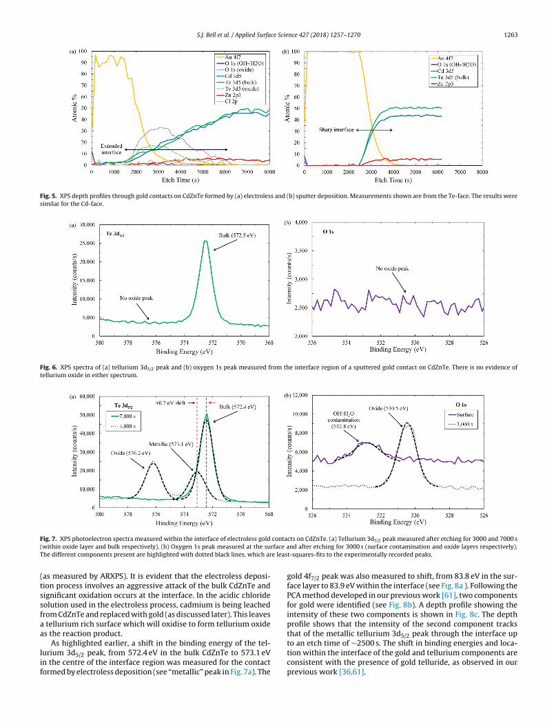
XPS depth profiles showing elemental and chemical state infor-mation from the surface and sub-surface regions of gold contactsformed by electroless and sputter deposition are presented in Fig. 5.The extended interface formed by electroless deposition (Fig. 5a)showed the presence of gold, oxygen, chlorine, cadmium and tel-lurium. The interface region was wider and more complex than thatformed by sputter deposition (Fig. 5b), which displayed a sharpinterface between the surface gold and bulk CdZnTe and no evi-dence of an oxide layer. The tellurium 3d5/2 and oxygen 1 s spectrameasured in the middle of the interface of the sputtered gold con-tact at an etch time of 3100 s are presented in Fig. 6. If an oxidelayer of a few nanometers in thickness had been present, it wouldhave been difficult to detect with the relatively long etch time of120 s per level used during the depth profile. Four additional depthprofiles with performed with a shorter etch time of 5 s per level(equivalent to the removal of ∼0.1 nm of gold per level). This isin the order of the native oxide thickness on bare CdZnTe mea-sured by ARXPS. Again no evidence of oxidation was found withinthe tellurium 3d5/2 or oxygen 1 s spectra at any point through thefour additional profiles. The native oxide formed on mechanicallypolished CdZnTe has already been shown to have a thickness of0.1–0.2 nm. Such a layer is unlikely to be observed following thesurface roughing and mixing induced by the argon ion sputtering.
During the XPS depth profile through the electroless gold con-tact interface region (see Fig. 5a), tellurium 3d5/2 and oxygen1 s components at different binding energies were observed (seeFig. 7). The lower binding energy tellurium 3d5/2 peak, correspond-ing to bulk CdZnTe, was measured throughout the interface region.The position of the peak shifted to higher energies nearer thesurface-side of the interface. A similar shift was also observed inour previous studies of electroless gold contacts, where the bindingenergy shift for both the tellurium 3d5/2 and gold 4f7/2 peaks wereconsistent with the presence of gold telluride [36,61]. This will bediscussed later. The higher binding energy 3d5/2 peak correspondedto tellurium oxide and was measured from 1500 to 5500 s.
The lower binding energy oxygen 1 s peak (Fig. 7b) wasattributed to tellurium oxide and was measured from 1500 to6500 s. The higher binding energy 1 s peak was attributed toOH−/H2O species present as contamination on the surface of thegold contact. After 120 s of etching this contamination peak wasremoved. Between 2500 and 3500 s, the OH−/H2O peak was againobserved. It was not unexpected to observe the presence of somehydrated species (metal hydroxides or hydrated metal oxides)within the interface due to the nature of deposition. The variationof the tellurium 3d5/2 oxide and O 1 s oxide peaks was related tothe variation in the stoichiometry of the tellurium oxide throughthe interface.
Through the tellurium oxide region (1500–5500 s) of the XPSdepth profile (Fig. 5a) the ratio of oxygen atoms bound in an oxidestate to tellurium atoms bound in an oxide state was measured toincrease, from ∼1.5 to ∼6. This ratio is an indication of the value of nin the stoichiometry relationship TeOn, with a value of n = 2 indicat-ing a phase of TeO2 and a value of n = 3 indicating a phase of TeO3or CdTeO3. The latter, CdTeO3, has been cited as being the moststable oxide formed on CdTe [62,63]. In the central region of theoxide, the ratio was approximately 2, indicating the oxide presentto mostly be TeO2. The increase in the value of n through the oxideregion confirmed that the composition of the oxide varied throughthe interface. After etching for ∼5000 s, n reached a value of 6; thismost likely resulted from the presence of oxidised cadmium chlo-ride corrosion products. A similar result was found in our recentanalysis of Redlen deposited gold contacts, with the company also
Fig. 2a and XPS depth profile in Fig. 5a confirmed the formation ofan interfacial oxide layer with a thickness of ∼250 nm. This is sig-nificantly larger than the native oxide layer found on bare CdZnTe
S.J. Bell et al. / Applied Surface Science 427 (2018) 1257–1270 1263
Fig. 5. XPS depth profiles through gold contacts on CdZnTe formed by (a) electroless and (b) sputter deposition. Measurements shown are from the Te-face. The results weresimilar for the Cd-face.
Fig. 6. XPS spectra of (a) tellurium 3d5/2 peak and (b) oxygen 1s peak measured from the interface region of a sputtered gold contact on CdZnTe. There is no evidence oftellurium oxide in either spectrum.
F conta( rface aT e leas
(tssfaa
lif
ig. 7. XPS photoelectron spectra measured within the interface of electroless goldwithin oxide layer and bulk respectively). (b) Oxygen 1s peak measured at the suhe different components present are highlighted with dotted black lines, which ar
as measured by ARXPS). It is evident that the electroless deposi-ion process involves an aggressive attack of the bulk CdZnTe andignificant oxidation occurs at the interface. In the acidic chlorideolution used in the electroless process, cadmium is being leachedrom CdZnTe and replaced with gold (as discussed later). This leaves
tellurium rich surface which will oxidise to form tellurium oxides the reaction product.
As highlighted earlier, a shift in the binding energy of the tel-urium 3d5/2 peak, from 572.4 eV in the bulk CdZnTe to 573.1 eVn the centre of the interface region was measured for the contactormed by electroless deposition (see “metallic” peak in Fig. 7a). The
cts on CdZnTe. (a) Tellurium 3d5/2 peak measured after etching for 3000 and 7000 snd after etching for 3000 s (surface contamination and oxide layers respectively).
t-squares-fits to the experimentally recorded peaks.
gold 4f7/2 peak was also measured to shift, from 83.8 eV in the sur-face layer to 83.9 eV within the interface (see Fig. 8a ). Following thePCA method developed in our previous work [61], two componentsfor gold were identified (see Fig. 8b). A depth profile showing theintensity of these two components is shown in Fig. 8c. The depthprofile shows that the intensity of the second component tracksthat of the metallic tellurium 3d5/2 peak through the interface up
to an etch time of ∼2500 s. The shift in binding energies and loca-tion within the interface of the gold and tellurium components areconsistent with the presence of gold telluride, as observed in ourprevious work [36,61].
1264 S.J. Bell et al. / Applied Surface Science 427 (2018) 1257–1270
Fig. 8. XPS and XPS-PCA photoelectron spectra measured within the interface of electroless gold contacts on CdZnTe for gold. (a) Gold 4f peak measured after etching for490 and 2450 s (within oxide layer and bulk respectively). (b) Oxygen 1 s peak measured at the surface and after etching for 3000 s (surface contamination and oxide layersrespectively). (c) Depth profile through the contact showing the relative intensity of each PCA component. The intensity of Au 4f PCA2 follows that of Te 3d5/2 PCA1 indicatingthe presence of gold telluride.
F cont( hlorii s.
wtfrrptr
ig. 9. XPS photoelectron spectra measured within the interface of electroless goldwithin oxide layer where chlorine was most intense and bulk, respectively). (b) Cntense). The broken lines are least-squares-fits of the chlorine 2p1/2 and 2p3/2 peak
A depletion of cadmium relative to tellurium (Tebulk + Teoxide)as measured within the extended interface region of the gold con-
act formed by electroless deposition (see Fig. 5a). The explanationor this is the greater difference in standard potential, �E0, for theeaction between cadmium and gold chloride, compared with theeaction between tellurium and gold chloride. This resulted in thereferential dissolution of cadmium from the CdZnTe substrate intohe solution during the electroless deposition. The two competing
eactions are presented below [15]:2AuCl−4 + 3CdSurface→2AuSurface + 8Cl− + 3Cd2+ E0 = +1.40V (14)
4AuCl−4 + 3TeSurface→4AuSurface + 16Cl− + 3Te4+ E0 = +0.43V (15)
acts on CdZnTe. (a) Cadmium 3d peak measured after etching for 4250 and 7000 sne 2p peak measured after etching for 4250 (where the chlorine signal was most
A variation in the binding energy of the cadmium 3d5/2 photo-electron peak, from 405.2 eV in the interface to 405.0 eV in the bulk,was observed during the depth profile of the gold contact formed byelectroless deposition (see Fig. 9a ). We concluded in our previousstudy of electroless gold contacts that such a shift was correlatedwith the presence of chloride and concluded that cadmium chloridewas present within the interface [61]. This was achieved by apply-ing principal component analysis to the XPS depth profile dataset.
In the current work, the chlorine 2p3/2 binding energy was mea-sured to be 198.3 eV, which was consistent with a metallic chloridespecies (see Fig. 9b). Using the PCA method, it was possible to con-
S.J. Bell et al. / Applied Surface Science 427 (2018) 1257–1270 1265
F s goldc d5/2 P
ficofspbdwrtw
(foTsowa.iacaast
ig. 10. XPS-PCA photoelectron spectra measured within the interface of electrolesontact showing the relative intensity of each PCA component. The intensity of Cd 3
rm the correlation between the presence of chlorine in a metalhloride state with the presence of cadmium bound in a compoundther than CdZnTe (see Fig. 10). This correlation was consistentlyound across the detectors investigated in the current study. Con-idering the reactions involved during the electroless depositionrocess, it would be expected that the CdZnTe is being attackedy Cl−. Precipitation of cadmium chloride at the etch front occursuring electroless deposition as the concentration of Cd2+ and Cl−
ithin the solution reach supersaturation levels. Chlorine has beeneported by other authors during the study of electroless gold con-acts [64–67]. It is likely that the chlorine observed in these studiesas also present as cadmium chloride.
The XPS depth profile through the electroless gold contactFig. 2a) indicated that gold was not just present as a discrete sur-ace layer, but had a diffusion tail extending through the telluriumxide/cadmium chloride region. In our previous studies [36,61],EM and FIB-SEM cross-section images of the interface region havehown the presence of gold particulates dispersed within the metalxide region. A TEM cross-section image taken from our previousork [61] showing the typical interfacial region which develops as
result of the electroless gold deposition process is given in Fig. 11a It has further been observed, in this work and our previous stud-es [36,61], that gold telluride is also present in the interface regionnd we have proposed that the gold particulates have an inner coreomprised of gold and outer layer of gold telluride. The chemicalnd structural characterization results of the interface region fromll of our work on gold contacts deposited on CdZnTe are very con-istent. A schematic illustration of the interface structure based onhe XPS/TEM results is shown in Fig. 11b.
contacts on CdZnTe for (a) cadmium and (b) chlorine. (c) Depth profile through theCA2 follows that of Cl 2p PCA1 indicating the presence of cadmium chloride.
3.3. Electronic properties (IV)
The room temperature (290 K) IV response of a typical CdZnTedetector with gold contacts fabricated by electroless depositionis presented in Fig. 12 and compared with a detector diced fromthe same CdZnTe crystal with gold contacts formed by sputterdeposition. At a field strength of −2000 Vcm−1 the detector withelectroless contacts produced a leakage current of −2.7 nAcm−2.This is equivalent to −1.7 pA per 250 �m2, well within the specifiedtolerance of the HEXITEC ASIC of 50 pA per channel and is suit-able for high resolution spectroscopic applications. The detectorwith sputtered contacts produced a comparably low negative biasleakage current of −4.4 nAcm−2 at −2000 Vcm−1. The positive biasleakage current produced by the detector with sputtered contactswas significantly elevated and would be sufficient to degrade thespectral resolution of the detector if operated with a positive biasor if the detector was mounted in the reverse configuration. Bothdetectors exhibited high room temperature resistivity; 5.1 ± 0.4and 2.73 ± 0.06 × 10¹⁰�.cm for the detector with electroless andsputtered contacts respectively, as calculated using Eq. (7). Despitethe two detectors being diced from the same crystal, their resis-tivity values differed by a factor of ∼2. The higher resistivity ofthe detector with gold contacts formed by electroless depositionwas the result of an additional series resistance introduced by thetellurium oxide based interface region.
The leakage current response of the detector with electrolesscontacts was symmetric and produced a characteristic “S-bend”[45], with Ohmic behaviour below ±1 Vcm−1. The leakage currentresponse of the detector with sputtered contacts also produced
an S-bend, however the response was asymmetric with the lowvoltage Ohmic region extending from −3 to +200 Vcm−1. Thebehaviour of both detectors outside of this low voltage regime is
1266 S.J. Bell et al. / Applied Surface Science 427 (2018) 1257–1270
Fig. 11. (a) TEM cross-section image taken of an electroless gold contact formedon a chemo-mechanically polished CdZnTe surface (Reproduced with permissionfe
bFatw[wOb
Fd
rom [61]). (b) Schematic illustration of the proposed interface structure formed bylectroless deposition of gold onto mechanically polished CdZnTe.
etter understood with reference to the log–log IV plots shown inig. 13. The negative bias response of both detectors between −30nd ∼ –200 Vcm−1 followed a ∼V1/2 dependency, indicating thathermal generation of carriers in the expanding depletion regionas the dominant leakage current mechanism in this voltage range
46,47]. At −200 Vcm−1, the voltage dependency switched to ∼V1,
ith a quasi-Ohmic response extending to −2000 Vcm−1. A quasi-hmic response is one where resistance R is linearly proportional,ut not equal, to V/I. For a true Ohmic response, Ohm’s Law mustig. 13. Log-log room temperature (290 K) IV plots from CdZnTe detectors with (a) eleepletion voltage VDepletion was determined from the crossover point of the two VX fits ap
Fig. 12. Typical room temperature IV response of CdZnTe detectors with gold con-tacts formed by electroless and sputter deposition. Insert: Low voltage regime.
stand. The change in voltage dependency indicated that full deple-tion had been reached at this voltage; VDepletion. The positive biasresponse of the detector with electroless contacts matched thenegative bias response. The positive bias response of the sputtercontacted detector above +200 Vcm−1 followed a ∼V1/2 depen-dency with no clear transition to a V1 dependent region. At thehighest applied positive bias (not shown in the plot), the volt-age dependency of the leakage current increased rapidly from V0.5
to V1.5. This suggested that injection from the contacts or evendielectric breakdown occurred soon after the detector became fullydepleted. If breakdown had occurred, it is likely to have beenlocated along the edge surfaces of the CdZnTe [68].
The leakage currents measured within the quasi-Ohmic regionsidentified above in Fig. 13 were diffusion limited. The effective bar-rier height between the contact and bulk CdZnTe is related to thediffusion-limited current according to Eq. (12). It is possible to cal-culate the effective barrier height by forming an Arrhenius plotof the temperature dependency of the leakage current at a fixedvoltage within the diffusion limited regime. The gradient of theArrhenius plot is equal to qEa/1000k, where Ea is the activationenergy of the process and in this case is equal to the effective bar-rier height. The temperature dependent IV measurements in therange of 260–340 K made on the CdZnTe detectors with electrolessand sputtered gold contacts are shown in Fig. 14. The leakage cur-rent measurements required for the Arrhenius plot were made at a
fixed voltage located within the quasi-Ohmic region over the rangeof temperatures investigated. The chosen voltages are identified bythe vertical dotted lines in Fig. 14.ctroless and (b) sputtered gold contacts for both positive and negative bias. Theplied to each data set.

S.J. Bell et al. / Applied Surface Science 427 (2018) 1257–1270 1267
Fig. 14. Log-log temperature dependent (260–340 K) IV plots for CdZnTe detectors with (acontacts under positive and negative bias respectively. The dotted vertical lines indicatewere extracted to form the Arrhenius plot used to determine the effective barrier height.
F
tAtotrsitai0
predicted by S-M. What follows is a closer examination of the four
ig. 15. Arrhenius plots of leakage current as a function of temperature (260–340 K).
The Arrhenius plots for the detectors with electroless and sput-ered contacts under positive and negative bias are shown in Fig. 15.
linear fit has been applied to each plot and the gradient was usedo calculate the effective barrier height. The effective barrier heightsf the detector with electroless contacts for negative and posi-ive bias were similar, with values of 0.83 ± 0.02 and 0.78 ± 0.04 eVespectively. The effective barrier height of the detector withputtered contacts for negative bias was 0.78 ± 0.02 eV and sim-lar to the electroless contacts. The effective barrier height of
he detector with sputtered contacts for positive bias was lowert 0.64 ± 0.02 eV. Other authors have reported barrier heightsn the range of 0.46–0.9 eV for electroless gold [56,69,70] and.73–0.95 eV for sputtered gold [70–72] contacts on high resistivity) & (b) electroless contacts under positive and negative bias and (c) & (d) sputtered the voltage (within the quasi-Ohmic region) at which the current measurements
CdZnTe. Drawing comparisons with published results is, however,difficult due to the many unknown surface preparation and depo-sition parameters associated with each study.
There are eight possible barriers across the Au/CdZnTe/Au detec-tor system; barriers for both carriers (electrons and holes) in bothdirections (in to and out of the semiconductor) at both contacts(gold on the Te- and Cd-faces). By making a series of simplearguments and referring to the barrier heights predicted by theSchottky-Mott (S-M) theory, it is possible to infer which barriereach measurement (presented in Fig. 15) related to. Firstly, the fourbarriers related to electron and hole transfer from the semicon-ductor into the metal at both contacts may be disregarded. This isbecause under sufficient bias the collecting contacts will be Ohmic,and the leakage current flowing through the detector will be lim-ited due to the barriers faced by electrons and holes entering theCdZnTe from the gold contacts. The n- or p-type nature of the leak-age current will depend on the relative heights of these barriersdue to the intrinsic high resistivity of the material. According tothe S-M theory, the electron and hole barrier heights should be0.80 and 0.77 eV respectively. This assumes a perfect gold contacton high resistivity Cd1-xZnxTe with the Fermi level pinned near mid-bandgap (Eg = 1.57/2 eV for x = 0.1 [73]) due to the compensation ofacceptors and donors [1]. The barrier heights measured for the elec-troless contacts under positive and negative bias, and the sputteredcontacts under negative bias were comparable with those predictedby S-M. The barrier height for the sputtered contacts under posi-tive bias was lower than either the electron or hole barrier height
barrier heights measured under positive and negative bias (appliedto the contact on the Te-face) to determine which of the remainingfour possible barriers each measurement related to.

1268 S.J. Bell et al. / Applied Surface Science 427 (2018) 1257–1270
Table 2Summary of the electronic properties of electroless and sputtered gold contacts extracted from IV measurements.
Electroless Sputtered
Resistivity (�.cm) 5.1 ± 0.4 × 10¹⁰ 2.73 ± 0.06 × 10¹⁰
Depletion voltage (V, at290 K)
60 (positive) n/a (positive)40 (negative) 60 (negative)
−1 −1
04 (po02 (ne
3
enfZedCcbrb
3
tsatcStrscdatrl
3
ppbtrwtcvcbpstmbhMtwtn
Leakage current (nA.cm , at −2000 V cm ) 2.7
Effective barrier heightn/p (eV)
0.78 ± 0.0.83 ± 0.
.3.1. Electroless − positive bias (0.78 ± 0.04 eV)Although the measured barrier height agreed well with both
lectron and hole barrier heights predicted by S-M, the theory tooko account of the significant oxide layer measured at the inter-
ace of either the Te or Cd-faces (see Fig. 5a). It was proposed byha et al. [18] that a CdTeO3 layer would create a large barrier forlectrons entering the CdZnTe from the gold contact but not hin-er the transport of holes. This is due to the low electron affinity ofdTeO3. It is the presence of the tellurium oxide layer that creates aonsistent barrier height for these contacts. It is concluded that thearrier height measured under positive bias was related to the bar-ier faced by holes entering the semiconductor from the positivelyiased contact on the Te-face of the crystal.
.3.2. Electroless gold − negative bias (0.83 ± 0.02 eV)As with the Te-face, a tellurium oxide layer was measured within
he interface of the contact on Cd-face following electroless depo-ition. As such the model proposed by Zha et al. [18] would againpply and the barrier height measured under negative bias relatedo the transfer of holes from the contact on Cd-face into the semi-onductor. This barrier was slightly greater than that predicted by-M and greater than the barrier at the Te-face. An n-type layer inhe CdZnTe below the oxide layer may explain this increase in bar-ier height. The XPS depth profile through the electroless contacthown in Fig. 5a confirmed the presence of chlorine and oxygenlose to the interface with the bulk CdZnTe. Chlorine is a knownonor dopant of CdTe [9,73] and oxygen has been proposed as anmphoteric dopant of CdTe, which may act as a donor or acceptoro compensate the majority carrier [74,75]. The diffusion of chlo-ine or oxygen into the bulk CdZnTe would have created an n-typeayer.
.3.3. Sputtered gold − positive bias (0.64 ± 0.02 eV)The barrier measured for the sputter contacted detector under
ositive bias was lower than both electron and hole barrier heightsredicted by S-M. Two scenarios may explain this: If the measuredarrier was an electron barrier (at the Cd-face), an n-type layer athe Cd-face would explain the reduced height. If the measured bar-ier was a hole barrier (at the Te-face), a p-type layer at the Te-faceould explain the reduced height. Morton et al. [56] proposed that
he diffusion of gold into the bulk would create a thin �-layer andalculated that a doping density of 109-10−11 cm−1 would raise thealence and conduction bands in the contact region of the semi-onductor. The increase in the valence band would decrease thearrier faced by holes entering the semiconductor. The XPS depthrofiles through sputtered contact shown in Fig. 5b appeared tohow a sharp interface between the contact and the bulk. Howeverhe junction was not fully abrupt and the tail of the gold signal was
easured to penetrate into the CdZnTe bulk. This tail may haveeen the result of surface roughness and non-uniformity or it mayave been due to diffusion of gold into the bulk as suggested byorton et al. It was not possible to determine if this gold penetra-
ion was greater at the Te-face due to the uncertainty associatedith the etch rate. It is also not clear why gold would preferen-
ially diffuse into the Te-face. Alternatively, it is proposed that an-type layer existed at the Cd-face and that the measured barrier
4.4sitive) 0.64 ± 0.02 (positive)gative) 0.78 ± 0.02 (negative)
height related to the barrier faced by electrons entering the semi-conductor from the contact at the Cd-face. The Cd-face is inherentlyCd-rich and will act as an n-layer through the effective presence oftellurium vacancies VTe and cadmium interstitials Cdi [76,77].
3.3.4. Sputtered gold − negative bias (0.78 ± 0.02 eV)The barrier height measured under negative bias was in good
agreement with both electron and hole barrier heights predicted byS-M. Two scenarios were suggested to explain the reduced barriermeasured under positive bias; an n-layer at the Cd-face or a p-layerat the Te-face. It was proposed that an n-layer at the Cd-face wasmore probable. An n-layer at the Cd-face would increase the barrierfor holes entering the CdZnTe from the contact on the Cd-face. Thiswas not reflected in the measured barrier height. It is proposedthat the barrier height measured under negative bias relates to thebarrier faced by electrons entering the CdZnTe from the contacton the Te-face. It would be expected that the Te-face would act asp-layer with the effective presence of cadmium vacancies VCd andtellurium interstitials Tei, in a similar manner to the Cd-face actingas an n-layer [76,77]. However the presence of a native oxide (TeO2)monolayer, as measured by ARXPS, would have acted as a small,additional barrier for both electrons and holes entering the CdZnTethrough the contact on the Te-face. This additional barrier wouldhave compensated for the intrinsically p-type nature of the Te-face.
A summary of the IV results is presented in Table 2. The detectorwith contacts formed by electroless deposition produced a sym-metric IV response. This was due to the innate polarity of the crystalhaving been degraded by the chemical etching of the CdZnTe sur-face and formation of the complex interface region. In contrast, thesputter deposition process has preserved the innate polarity of thecrystal and produced an asymmetric IV response.
4. Conclusions and summary
Gold contacts deposited by electroless and sputter depositionon (111) orientated single-crystal CdZnTe have been investigated.The inhomogeneous structure, chemical composition and elec-tronic response of the contacts have been measured following amulti-technique characterization approach, including AFM, SEM,FIB, (AR)XPS and IV methods. The primary findings are as follows:
• The electroless deposition of gold onto mechanically polishedCdZnTe formed a rough surface gold layer with an averageuniform base thickness of 65 nm but with regular asperitiesextending an average of 54 nm above the base layer. A wideinterface region mostly comprised of tellurium oxide was foundbetween the CdZnTe bulk and the gold layer. However a thinnerlayer of cadmium chloride was observed at the interface betweenthe oxide and the CdZnTe and gold/gold telluride particulates alsoexisted within this interface region.
• The gold layer formed by sputter deposition was found to have
a generally smoother base morphology, but many particulateswere observed protruding from the surface, giving rise to a higherRMS roughness than that of the electroless deposited gold layer.A sharp interface was observed between the gold layer and bulk
ce Scie
•
•
•
tinwiComi
A
mSiEULF
R
[
[
[
[
[
[
[
[
[
[
[
[
[
[
[
[
[
[
[
[
[
S.J. Bell et al. / Applied Surfa
CdZnTe and no evidence of oxidation beyond that of the CdZnTenative oxide.ARXPS measurements on bare, mechanically polished CdZnTeindicated the presence of a native oxide prior to contact depo-sition. The oxide layer was measured to be 0.20 ± 0.01 nm on theTe-face and 0.11 ± 0.01 nm on the Cd-face.The detector with electroless contacts can be described as twoback-to-back diodes with a series resistance in between. The elec-troless deposition process is an aggressive chemical treatmentwhich effectively degraded the definition of the (111) face on themechanically polished CdZnTe. As a result, the structure and IVresponse of these contacts were symmetric. This compared withsputter deposition which preserved the (111) face definition andproduced an asymmetric IV response.The barrier heights measured under positive and negative biaswere consistent with the hole barrier height predicted by theSchottky-Mott theory for the detector with electroless contacts.This was due to the presence of a thick tellurium oxide layerwhich acted as a large barrier to electrons entering the CdZnTebut not holes. The barrier height measured under positive biasapplied to the sputter deposited contact was lower than that pre-dicted by Schottky-Mott. It was proposed that the inherent n-typenature of the Cd-face, through the effective presence of telluriumvacancies VTe and cadmium interstitials Cdi, was responsible forlowering the electron barrier. The barrier at the sputtered goldcontact measured under negative bias was controlled by thenative oxide on the Te-face, which compensated for the inherentp-type nature of this face.
Developing a deposition method which provides a durable con-act and maximises the spectroscopic performance of the detectors vital if CdZnTe X/�-ray imagers are to replace traditional tech-ologies. This research, together with our previous characterizationork, provides a good understanding of the metal-semiconductor
nterface formed when depositing gold contacts with varyingdZnTe preparation procedures, deposition parameters and meth-ds. The work represents an important step in optimization of theetal-semiconductor interface which currently is a limiting factor
n the development of high resolution CdZnTe detectors.
cknowledgments
The authors would like to thank Dr David Cox, Dr Veera-ani Perumal, Dr Steven Hinder, Dr Peter Wilson, Chris Burt and
ujit Gurung of the University of Surrey for their assistance dur-ng this work. This research was funded by the EPSRC (grantP/G037388/1) via the MiNMaT Industrial Doctorial Centre of theniversity of Surrey in collaboration with the Rutherford Appletonaboratory’s Centre for Instrumentation (Science and Technologyacilities Council).
eferences
[1] T.E. Schlesinger, J.E. Toey, H. Yoon, E.Y. Lee, B.A. Brunett, L. Franks, R.B. James,Cadmium zinc telluride and its use as a nuclear radiation detector material,Mater. Sci. Eng. R: Rep. 32 (2001) 103–189.
[2] K. Iniewski, CZT sensors for Computed Tomography: from crystal growth toimage quality, J. Instrum. 11 (2016) C12034.
[3] C. Szeles, S.A. Soldner, S. Vydrin, J. Graves, D.S. Bale, CdZnTe semiconductordetectors for spectroscopic X-ray imaging, IEEE Trans. Nucl. Sci. 55 (1) (2008)572–582.
[4] S.D. Sordo, L. Abbene, E. Caroli, A.M. Mancini, A. Zappettini, P. Ubertini,Progress in the devleopment of CdTe and CdZTe semiconductor radiation
detectors for astrophysical and medical applications, Sensors 9 (5) (2009)3491–3526.[5] L. Li, R. Li, S. Zhang, Z. Chen, Simultaneous X-ray fluorescence and K-edge CTimaging with photon-counting detectors, Proceedings of SPIE 9967:Developments in X-ray Tomography X, 99670F (2016).
[
nce 427 (2018) 1257–1270 1269
[6] T. Billoud, C. Leory, C. Papadatos, M. Pichotka, S. Pospisil, J.S. Roux,Characterization of a pixelated CdTe Timepix detector operated in ToT mode,J. Instrum. 12 (2017) P01018.
[7] S. Basolo, J.F. Bérar, N. Boudet, P. Breugnon, B. Chantepie, J.C. Clémens, P.Delpierre, B. Dinkespiler, S. Hustache, K. Medjoubi, M. Ménouni, C. Morel, P.Pangaud, E. Vigeolas, A 20 kpixels CdTe photon-counting imager using XPADchip, nuclear instruments and methods in physics research section A:accelerators, spectrometers, Detectors Associated Equipment 589 (2) (2008)268–274.
[8] P. Seller, S.J. Bell, R. Cernik, C. Christodoulou, C.K. Egan, J.A. Gaskin, S. Jacques,S. Pani, B.D. Ramsey, C. Reid, P.J. Sellin, J.W. Scuffham, R.D. Speller, M.D.Wilson, M.C. Veale, Pixellated Cd(Zn)Te high-energy X-ray instrument, J.Instrum. 6 (2011) C12009.
[9] M. Funaki, Y. Ando, R. Jinnai, A. Tachibana, R. Ohno, Development of CdTedetectors in acrorad, Proceedings of the International Workshop onSemiconductor PET (2007).
10] F. Principato, A.A. Turturici, M. Gallo, L. Abbene, Polarization phenomena inAl/p-CdTe/Pt X-ray detectors, Nucl. Instrum. Methods Phys. Res. A 730 (2013)141–145.
11] F. Zhang, W.R. Kaye, Z. He, Performance of 3-D position sensitive CdZnTedetectors for gamma-Ray energies above 1 MeV, in: B. Yu (Ed.), 2009 IEEENuclear Science Symposium Conference Record, IEEE, 2009, p. 2012.
12] H.B. Michaelson, The work function of the elements and its periodicity, J.Appl. Phys. 48 (1977) 4729.
13] W. Sang, J. Wei, Z. Qi, L. Wanwan, M. Jiahua, T. Jianyong, Q. Yongbiao, Primarystudy on the contact degradation mechanism of CdZnTe detectors, Nucl.Instrum. Methods Phys. Res. A 527 (2004) 487–492.
14] Q. Zheng, F. Dierre, V. Corregidor, J. Crocco, H. Bensalah, J.L. Plaza, E. Alves, E.Dieguez, Electroless deposition of Au, Pt, or Ru metallic layers on CdZnTe,Thin Solid Films 525 (2012) 56–63.
15] Q. Zheng, F. Dierre, J. Franc, J. Crocco, H. Bensalah, V. Corregidor, E. Alves, E.Ruiz, O. Vela, J.M. Perez, E. Dieguez, Investigation of generation of defects dueto metallization on CdZnTe detectors, J. Phys. D: Appl. Phys. 45 (17) (2012).
16] S.H. Lee, I.J. Kim, Y.J. Choi, J.K. Hong, H.K. Lee, Y.C. Chung, Y. Yi, S.U. Kim, M.J.Park, The comparison on the performance of a gamma-ray spectrometer withthe variation of Pt(Au)/CdZnTe/Pt(Au) interface, J. Cryst. Growth 214/215(2000) 1111–1115.
17] L. Wang, W. Sang, W. Shi, Y. Qian, J. Min, D. Liu, Y. Xia, Electrical properties ofcontacts on P-type Cd0.8Zn0.2Te crystal surfaces, Nucl. Instrum. MethodsPhys. Res. A 448 (2000) 581–585.
18] G. Zha, W. Jie, T. Tan, W. Zhang, F. Xu, The interface reaction and schottkybarrier between metals and CdZnTe, J. Phys. Chem. C 111 (2007)12834–12838.
19] A. Burger, H. Chen, J. Tong, D. Shi, M.A. George, K.T. Chen, W.E. Collins, R.B.James, C.M. Stahle, L.M. Bartlett, Investigation of electrical contacts forcd1-xZnxTe nuclear radiation detectors, IEEE T Nucl Sci 44 (3) (1997)934–938.
20] Veale, M.C. 2014, 02/05/2016-last update, HEXITEC [Online]. Available: http://en.wikipedia.org/wiki/HEXITEC [18/05/2017].
21] L.L. Jones, P. Seller, M.D. Wilson, A. Hardie, HEXITEC ASIC − a pixellatedreadout chip for CZT detectors, Nucl. Instrum. Methods Phys. Res. A 604(2009) 34–37.
22] M.D. Wilson, R. Cernik, H. Chen, C. Hansson, K. Iniewski, L.L. Jones, P. Seller,M.C. Veale, Small pixel CZT detector for hard X-ray spectroscopy, Nucl.Instrum. Methods Phys. Res. A 652 (2011) 158–161.
23] M.C. Veale, S.J. Bell, L.L. Jones, P. Seller, M.D. Wilson, C. Allwork, D. Kitou, P.Sellin, P. Veeramani, R. Cernik, An ASIC for the study of charge sharing effectsin small pixel CdZnTe X-Ray detectors, IEEE Trans. Nucl. Sci. 58 (5) (2011)2357–2362.
24] C. Allwork, D. Kitou, S. Chaudhuri, P.J. Sellin, P. Seller, M.C. Veale, N. Tartoni, V.Perumal, X-ray beam studies of charge sharing in small pixel, spectroscopic,CdZnTe detectors, IEEE Trans. Nucl. Sci. 59 (4) (2012) 1563–1568.
25] M.D. Wilson, L. Dummott, D.D. Duarte, F.H. Green, S. Pani, A. Schneider, J.W.Scuffham, P. Seller, M.C. Veale, A 10 cm x 10 cm CdTe spectroscopic imagingdetector based on the HEXITEC ASIC, J. Instrum. 10 (2015) P10011.
26] M.C. Veale, S.J. Bell, P. Seller, M.D. Wilson, V. Kachkanov, X-ray micro-beamcharacterization of a small pixel spectroscopic CdTe detector, J. Instrum. 7(2012) P07017.
27] F.H. Green, M.C. Veale, M.D. Wilson, P. Seller, J. Scuffham, S. Pani, Scatter freeimaging for the improvement of breast cancer detection in mammography,Phys. Med. Biol. 61 (20) (2016) 7246–7262.
28] J.W. Scuffham, S. Pani, P. Seller, P.J. Sellin, M.C. Veale, M.D. Wilson, R. Cernik,Imaging of Ra-223 with a small-pixel CdTe detector, J. Instrum. 10 (2015)C01029.
29] S.M. Alkhateeb, M.H. Abdelkader, D.A. Bradley, P. Seller, M.C. Veale, M.D.Wilson, S. Pani, Energy dispersive X-ray diffraction computed tomography ofBreast-simulating phantoms and a tissue sample, Proceedings of SPIE 8668,86684G (2013).
30] D. O’Flynn, C. Crews, I. Drakos, C. Christodoulou, M.D. Wilson, M.C. Veale, P.Seller, R.D. Speller, Materials identification using a small-scale pixellatedX-ray diffraction system, J. Phys. D: Appl. Phys. 49 (2016) 175304.
31] D. O’Flynn, H. Desai, C. Reid, C. Christodoulou, M.D. Wilson, M.C. Veale, P.Seller, D. Hills, B. Wong, R.D. Speller, Identification of simulants for explosivesusing pixellated X-ray diffraction, Crime Sci. 2 (2013) 4.

1 ce Scie
[
[
[
[
[
[
[
[
[
[
[
[
[
[
[
[
[
[
[
[
[
[
[
[
[
[
[
[
[
[
[
[
[
[
[
[
[
[
[
[
[
[
[
[
[76] A. Castaldini, A. Cavallini, B. Fraboni, P. Fernandez, J. Piqueras, Deep energylevels in CdTe and CdZnTe, J. Appl. Phys. 83 (4) (1998) 2121–2126.
270 S.J. Bell et al. / Applied Surfa
32] C.K. Egan, S.D.M. Jacques, T. Connolley, M.D. Wilson, M.C. Veale, P. Seller, R.J.Cernik, Dark-field hyperspectral X-ray imaging, Proceedings of The RoyalSociety A 470 (2014) 20130629.
33] E. Liotti, et al., Mapping of multi-elements during melting and solidificationusing synchrotron X-rays and pixel-based spectroscopy, Nat. Sci. Rep. 5(2015) 15988.
34] C. Egan, et al., 3D chemical imaging in the laboratory by hyperspectral X-raycomputed tomography, Nat. Sci. Rep. 5 (2015) 15979.
35] M. Amman, J.S. Lee, P.N. Luke, H. Chen, S.A. Awadalla, R. Redden, G. Bindley,Evaluation of THM-grown CdZnTe material for large-volume gamma-raydetector applications, IEEE Trans. Nucl. Sci. 56 (3) (2009) 795–799.
36] S.J. Bell, M.A. Baker, D.D. Duarte, A. Schneider, P. Seller, P.J. Sellin, M.C. Veale,M.D. Wilson, Characterization of the metal-semiconductor interface of goldcontacts on CdZnTe formed by electroless deposition, J. Phys. D: Appl. Phys.48 (27) (2015).
37] M. Roumie, M. Hage-Ali, K. Zahraman, B. Nsouli, G. Younes, Characterizationof electroless Au, Pt, and Pd contacts on CdTe and ZnTe by RBS and SIMStechniques, Nucl. Instrum. Methods Phys. Res. B 219 (2004) 871–874.
38] S. Babar, P.J. Sellin, J.F. Watts, M.A. Baker, An XPS study of bromine in methanoletching and hydrogen peroxide passivation treatments for cadmium zinctelluride radiation detectors, Appl. Surf. Sci. 264 (2013) 681–686.
39] J.F. Moulder, W.F. Stickle, P.E. Sobol, K.D. Bomben, Handbook of X-rayPhotoelectron Spectroscopy, Physical Electronics Inc, Minnesota, USA, 1995.
40] Thermo Scientific 2015, Avantage. Available: https://www.thermofisher.com/order/catalog/product/IQLAADGACKFAKRMAVI?ICID=search-product[2016,08/16].
41] J.F. Watts, J. Wolstenholme, An Introduction to Surface Analysis by XPS andAES, Wiley, West Sussex, UK, 2003.
42] K. Artyushkova, J.E. Fulghum, Idenification of chemical components in XPSspectra and images using multivariate statistical analysis methods, J. ElectronSpectrosc. Relat. Phenom. 121 (2001) 33–55.
43] Thermo Scientific 2008, Angle Resolved XPS. Available:https://tools.thermofisher.com/content/sfs/brochures/D16069∼.pdf[2016,08/16].
44] M.P. Seah, Simple universal curve for the energy-dependent electronattenuation length for all materials, Surf. Interface Anal. 44 (10) (2012)1353–1359.
45] A.E. Bolotnikov, S.E. Boggs, C.M.H. Chen, W.R. Cook, F.A. Harrison, S.M.Schindler, Properties of Pt schottky type contacts on high-resistivity CdZnTedetectors, Nucl. Instrum. Methods Phys. Res. A 482 (2002) 395–407.
46] B. Streetman, S. Banerjee, Solid State Electronic Devices, 6th edn, PrenticeHall, 2005.
47] A. Cola, I. Farella, Electric fields and dominant carrier transport mechanismsin CdTe schottky detectors, Appl. Phys. Lett. 102 (2013) 113502.
48] A.E. Bolotnikov, G.S. Camarda, G.W. Wright, R.B. James, Factors limiting theperformance of CdZnTe detectors, IEEE Trans. Nucl. Sci. 52 (3) (2005) 589–598.
49] A. Rose, Space-charge-limited currents in solids, Phys. Rev. 97 (6) (1955)1538–1544.
50] M.A. Lampert, Volume-controlled current injection in insulators, Rep. Prog.Phys. 27 (1) (1964) 329–367.
51] A.A. Turturici, L. Abbene, G. Gerardi, F. Principato, Electrical characterizationof CdTe pixel detectors with Al schottky anode, Nucl. Instrum. Methods Phys.Res. A 763 (2014) 476–482.
52] V.L.A. Kosyachenko, T. Aoki, C.P. Lambropoulos, V.A. Gnatyuk, E.V. Grushko,V.M. Sklyarchuk, O.L. Maslyanchuk, O.F. Sklyarchuk, A. Koike, High energyresolution CdTe schottky diode y-Ray detectors, in: Nuclear ScienceSymposium and Medical Imaging Conference, Anaheim, Ca USA, 2012, p. 4156.
53] Zeghbroeck, B.V. 2011. Principles of Semiconductor Devices [Homepage ofUniversity of Colorado at Boulder], [Online]. Available:
http://ecee.colorado.edu/∼bart/book/book/title.htm [2015, 02/14].54] W. Schottky, Zur halbleitertheorie der sperrschicht- und spitzengleichrichter,Z. Angew. Phys. 113 (5–6) (1939) 367–414.
55] N.F. Mott, The theory of crystal rectifiers, Proceedings of the Royal Society A171 (1939) 27–38.
[
nce 427 (2018) 1257–1270
56] E.J. Morton, M.A. Hossain, P. De Antonis, A.M.D. Ede, Investigation ofAu-CdZnTe contacts using photovoltaic measurement, Nucl. Instrum.Methods Phys. Res. A 458 (2001) 558–562.
57] C.R. Crowell, S.M. Sze, Current transport in metal-semiconductor barriers,Solid-State Electron. 9 (1966) 1035–1048.
58] R.T. Tung, Recent advances in schottky barrier concepts, Mater. Sci. Eng. R 35(2001) 1–138.
59] C.- Wu, Interfacial layer-thermionic-diffusion theory for the schottky barrierdiode, J. Appl. Phys. 53 (1982) 5947–5950.
60] H. Chen, A. Awadalla, P. Marthandam, K. Iniewski, P.H. Lu, G. Bindley, in: R.B.James, L.A. Franks, A. Burger (Eds.), CZT Device with Improved Sensitivity forMedical Imaging and Homeland Security Applications, Hard X-Ray,Gamma-Ray, and Neutron Detector Physics XI, SPIE, Washington, USA, 2009.
61] S.J. Bell, M.A. Baker, H. Chen, P. Marthandam, V. Perumal, A. Schneider, P.Seller, P.J. Sellin, M.C. Veale, M.D. Wilson, A multi-technique characterizationof electroless gold contacts on single crystal CdZnTe radiation detectors, J.Phys. D: Appl. Phys. 46 (2013) 455502.
62] D.R. Rhiger, R.E. Kvaas, Solid-state quaternary phase equilibrium diagram forthe Hg–Cd–Te–O system, J. Vac. Sci. Technol. A 1 (no. 3) (1983) 1712–1718.
63] A. Burger, H. Chen, K. Chattopadhyay, D. Shi, S.H. Morgan, W.E. Collins, R.B.James, Characterization of metal contacts on and surfaces of cadmium zinctelluride, Nucl. Instrum. Methods Phys. Res. A 428 (1999) 8–13.
64] T.J. Magee, J. Peng, J. Bean, Microscopic defects and infrared absorption incadmium telluride, Phys. Status Solidi (A) 27 (1975) 557.
65] O.A. Matveev, A.I. Terent’ev, Basic principles of postgrowth annealing ofCdTe:Cl ingot to obtain semi-insulating crystals, Electron. Optic. Prop.Semicond. 34 (11) (2000) 1264–1269.
66] Y. Marfaing, Impurity doping and compensation mechanisms in CdTe, ThinSolid Films 387 (2001) 123–128.
67] V.D. Popovych, I.S. Virta, F.F. Sizovc, V.V. Tetyorkinc, Z.F. Tsybrii, L.O. Darchuk,O.A. Parfenjuk, M.I. Ilashchuk, The effect of chlorine doping concentration onthe quality of CdTe single crystals grown by the modified physical vaportransport method, J. Cryst. Growth 308 (2007) 63–70.
68] D.D. Duarte, S.J. Bell, J. Lipp, A. Schneider, P. Seller, M.C. Veale, M.D. Wilson,M.A. Baker, P.J. Sellin, V. Kachkanov, K.J.S. Sawhney, Edge effects in a smallpixel CdTe for X-ray imaging, J. Instrum. 8 (2013) P10018.
69] P. Veeramani, M. Haris, S. Moorthy Babu, Investigation of CdTex andcd1-xZnxTe schottky barrier diode structure based �-ray detectors, Mater.Manuf. Processes 22 (2007) 375–378.
70] X.Y. Liang, J.H. Min, J. Chen, D. Wang, H. Li, Y. Wang, L.J. Wang, J.J. Zhang,Metal/semiconductor contacts for schottky and photoconductive CdZnTedetector, Phys. Procedia 32 (2012) 545–550.
71] K. Chattopadhyay, Z. Ma, J. Ndap, A. Burger, T.E. Schlesinger, M. Greaves, H.L.Glass, J.P. Flint, R.B. James, Thermal treatments of CdTe and CdZnTe detectors,in: Proceeedings of SPIE 4141, Hard X-ray, Gamma-Ray, and Neutron DetectorPhysics II, 303 SPIE, San Diego, 2000.
72] Q. Li, J. Wanqi, L. Fu, X. Zhang, X. Wang, X. Bai, G. Zha, Investigation on theelectrical properties of metal-Cd0.9Zn0.1Te contacts, Mater. Sci. Eng. B 135(2006) 15–19.
73] M. Fiederle, V. Babentsov, J. Franc, A. Fauler, J.- Konrath, Growth of highresistivity CdTe and (Cd, Zn)Te crystals, Cryst. Res. Technol. 38 (7–8) (2003)588–598.
74] T.M. Hsu, R.J. Jih, P.C. Lin, H.Y. Ueng, Y.J. Hsu, H.L. Hwang, Oxygen doping inclose-spaced-sublimed CdTe thin films for photovoltaic cells, J. Appl. Phys. 59(1986) 3607.
75] M. Du, H. Takenaka, D.J. Singh, Carrier compensation in semi-insulating CdTe:first-principles calculations, Phys. Rev. B 77 (094122) (2008) 1–5.
77] I.M. Dharmadasa, Review of the CdCl2 treatment used in CdS/CdTe thin filmsolar cell development and new evidence towards improved understanding,Coatings 4 (2014) 282–307.