Applied Surface Science - SKKUweb.skku.edu/~nmdl/publication/2013/(Applied surface Science... ·...
7
Applied Surface Science 271 (2013) 32–38 Contents lists available at SciVerse ScienceDirect Applied Surface Science jou rn al h om epa g e: www.elsevier.com/locate/apsusc Effect of buffer layer deposition on diameter and alignment of carbon nanotubes in water-assisted chemical vapor deposition Shashikant P. Patole a,b,∗∗,1 , Jae-Hun Jeong a,1 , Seong Man Yu b , Ha-Jin Kim c , Jae-Hee Han d , In-Taek Han c , Ji-Beom Yoo a,b,∗ a School of Advanced Materials Science and Engineering, Sungkyunkwan University, Suwon 440746, Republic of Korea b SKKU Advanced Institute of Nanotechnology (SAINT), Sungkyunkwan University, Suwon 440746, Republic of Korea c Materials Application Group, Samsung Advanced Institute of Technology (SAIT), Yongin-si 446712, Republic of Korea d Department of Energy IT, Gachon University, Seongnam 461701, Republic of Korea a r t i c l e i n f o Article history: Received 24 May 2012 Received in revised form 12 December 2012 Accepted 25 December 2012 Available online 7 January 2013 Keywords: Carbon nanotubes Buffer layer Catalyst Surface topography Growth mechanism a b s t r a c t Vertically aligned carbon nanotubes (CNTs) grown by water-assisted chemical vapor deposition have revealed differences in structure and morphology depending on the deposition rate of the Al buffer layer. Rearrangement of the Fe catalyst during CNT growth is mainly influenced by the buffer layer topography, which in turn depends on the buffer layer deposition rate. A higher deposition rate makes the substrate rougher and causes the growth of more aligned, low diameter CNTs with greater height. In contrast, slow deposition results in a smooth surface, which grows misaligned, large diameter CNTs with less height. Based on the results, a CNT growth model has been proposed. © 2012 Elsevier B.V. All rights reserved. 1. Introduction The recent advance in the growth of vertically aligned carbon nanotubes (CNTs) by chemical vapor deposition (CVD) promises various novel applications such as high strength yarns, multi- functional scrolls, torsional artificial muscles, electron emitters, viscoelastic materials, etc. [1–5]. In such applications, the key nanoscale characteristics of CNTs, such as diameter, packing, and alignment, as well as their collective order and arrangement at higher length scales, must be controlled. Despite the interest in the controlled growth of carbon nanotubes, several long-standing questions remain about how ensembles of catalyst nanoparticles respond to processing variables such as choice of substrates, choice of buffer layers, choice of catalyst, growth temperature, gas flux, choice of hydrocarbon gas, and partial pressure. Factors controlling the nucleation efficiency, diameter, wall number, alignment and ∗ Corresponding author at: School of Advanced Materials Science and Engineering, Sungkyunkwan University, Suwon 440746, Republic of Korea. ∗∗ Corresponding author at: School of Advanced Materials Science and Engineering, Sungkyunkwan University, Suwon 440746, Republic of Korea. Tel.: +82 31 299 4745; fax: +82 31 290 7410. E-mail addresses: [email protected] (S.P. Patole), [email protected] (J.-B. Yoo). 1 These authors contributed equally to this paper. chirality of nanotubes remain critical not only for vertically aligned nanotube forests, where macroscopic parameters are developed, such as inter connected nanotubes for spin-capable CNTs, but also in nanoscale electronics, where individual nanotubes are desired. A variety of parameters can affect nanotube diameter and qual- ity, including the substrate, buffer layer, catalyst composition, type of feedstock gas, partial pressure of feedstock gas, annealing, effects of oxidant or inert background gas, etc. [6–18]. The annealing and gas environment deeply influence the catalyst size distribution, which determines the morphologies of the corresponding CNT arrays [13]. The partial pressure of the carbon feedstock has also been shown to play a major role [14–18]. Cheung et al. showed not only that catalyst particle size governs the diameter of resultant nanotubes but also noted the important role that reactant partial pressure plays in determining the distribution of nanotube diame- ters that grow from polydisperse particles [14]. Larger diameter nanoparticles were shown to require higher partial pressure to nucleate and grow correspondingly larger diameter nanotubes. Lu et al. showed that by lowering not only the carbon feedstock rate but also the temperature, small diameter single wall CNTs could selectively be grown from a wide distribution of catalyst nanopar- ticle diameters and proposed an optimal carbon feeding rate to grow single wall CNTs from different diameter nanoparticles, with overfed nanoparticles shutting down growth due to over coating with carbon and underfed particles never nucleating [15]. In water 0169-4332/$ – see front matter © 2012 Elsevier B.V. All rights reserved. http://dx.doi.org/10.1016/j.apsusc.2012.12.129
Transcript of Applied Surface Science - SKKUweb.skku.edu/~nmdl/publication/2013/(Applied surface Science... ·...

Ei
SIa
b
c
d
a
ARR1AA
KCBCSG
1
nvfvnahtqroct
S
Sf
0h
Applied Surface Science 271 (2013) 32– 38
Contents lists available at SciVerse ScienceDirect
Applied Surface Science
jou rn al h om epa g e: www.elsev ier .com/ locate /apsusc
ffect of buffer layer deposition on diameter and alignment of carbon nanotubesn water-assisted chemical vapor deposition
hashikant P. Patolea,b,∗∗,1, Jae-Hun Jeonga,1, Seong Man Yub, Ha-Jin Kimc, Jae-Hee Hand,n-Taek Hanc, Ji-Beom Yooa,b,∗
School of Advanced Materials Science and Engineering, Sungkyunkwan University, Suwon 440746, Republic of KoreaSKKU Advanced Institute of Nanotechnology (SAINT), Sungkyunkwan University, Suwon 440746, Republic of KoreaMaterials Application Group, Samsung Advanced Institute of Technology (SAIT), Yongin-si 446712, Republic of KoreaDepartment of Energy IT, Gachon University, Seongnam 461701, Republic of Korea
r t i c l e i n f o
rticle history:eceived 24 May 2012eceived in revised form2 December 2012ccepted 25 December 2012vailable online 7 January 2013
a b s t r a c t
Vertically aligned carbon nanotubes (CNTs) grown by water-assisted chemical vapor deposition haverevealed differences in structure and morphology depending on the deposition rate of the Al buffer layer.Rearrangement of the Fe catalyst during CNT growth is mainly influenced by the buffer layer topography,which in turn depends on the buffer layer deposition rate. A higher deposition rate makes the substraterougher and causes the growth of more aligned, low diameter CNTs with greater height. In contrast, slow
eywords:arbon nanotubesuffer layeratalyst
deposition results in a smooth surface, which grows misaligned, large diameter CNTs with less height.Based on the results, a CNT growth model has been proposed.
© 2012 Elsevier B.V. All rights reserved.
urface topographyrowth mechanism
. Introduction
The recent advance in the growth of vertically aligned carbonanotubes (CNTs) by chemical vapor deposition (CVD) promisesarious novel applications such as high strength yarns, multi-unctional scrolls, torsional artificial muscles, electron emitters,iscoelastic materials, etc. [1–5]. In such applications, the keyanoscale characteristics of CNTs, such as diameter, packing, andlignment, as well as their collective order and arrangement atigher length scales, must be controlled. Despite the interest inhe controlled growth of carbon nanotubes, several long-standinguestions remain about how ensembles of catalyst nanoparticlesespond to processing variables such as choice of substrates, choice
f buffer layers, choice of catalyst, growth temperature, gas flux,hoice of hydrocarbon gas, and partial pressure. Factors controllinghe nucleation efficiency, diameter, wall number, alignment and∗ Corresponding author at: School of Advanced Materials Science and Engineering,ungkyunkwan University, Suwon 440746, Republic of Korea.∗∗ Corresponding author at: School of Advanced Materials Science and Engineering,ungkyunkwan University, Suwon 440746, Republic of Korea. Tel.: +82 31 299 4745;ax: +82 31 290 7410.
E-mail addresses: [email protected] (S.P. Patole), [email protected] (J.-B. Yoo).1 These authors contributed equally to this paper.
169-4332/$ – see front matter © 2012 Elsevier B.V. All rights reserved.ttp://dx.doi.org/10.1016/j.apsusc.2012.12.129
chirality of nanotubes remain critical not only for vertically alignednanotube forests, where macroscopic parameters are developed,such as inter connected nanotubes for spin-capable CNTs, but alsoin nanoscale electronics, where individual nanotubes are desired.
A variety of parameters can affect nanotube diameter and qual-ity, including the substrate, buffer layer, catalyst composition, typeof feedstock gas, partial pressure of feedstock gas, annealing, effectsof oxidant or inert background gas, etc. [6–18]. The annealing andgas environment deeply influence the catalyst size distribution,which determines the morphologies of the corresponding CNTarrays [13]. The partial pressure of the carbon feedstock has alsobeen shown to play a major role [14–18]. Cheung et al. showed notonly that catalyst particle size governs the diameter of resultantnanotubes but also noted the important role that reactant partialpressure plays in determining the distribution of nanotube diame-ters that grow from polydisperse particles [14]. Larger diameternanoparticles were shown to require higher partial pressure tonucleate and grow correspondingly larger diameter nanotubes. Luet al. showed that by lowering not only the carbon feedstock ratebut also the temperature, small diameter single wall CNTs couldselectively be grown from a wide distribution of catalyst nanopar-
ticle diameters and proposed an optimal carbon feeding rate togrow single wall CNTs from different diameter nanoparticles, withoverfed nanoparticles shutting down growth due to over coatingwith carbon and underfed particles never nucleating [15]. In water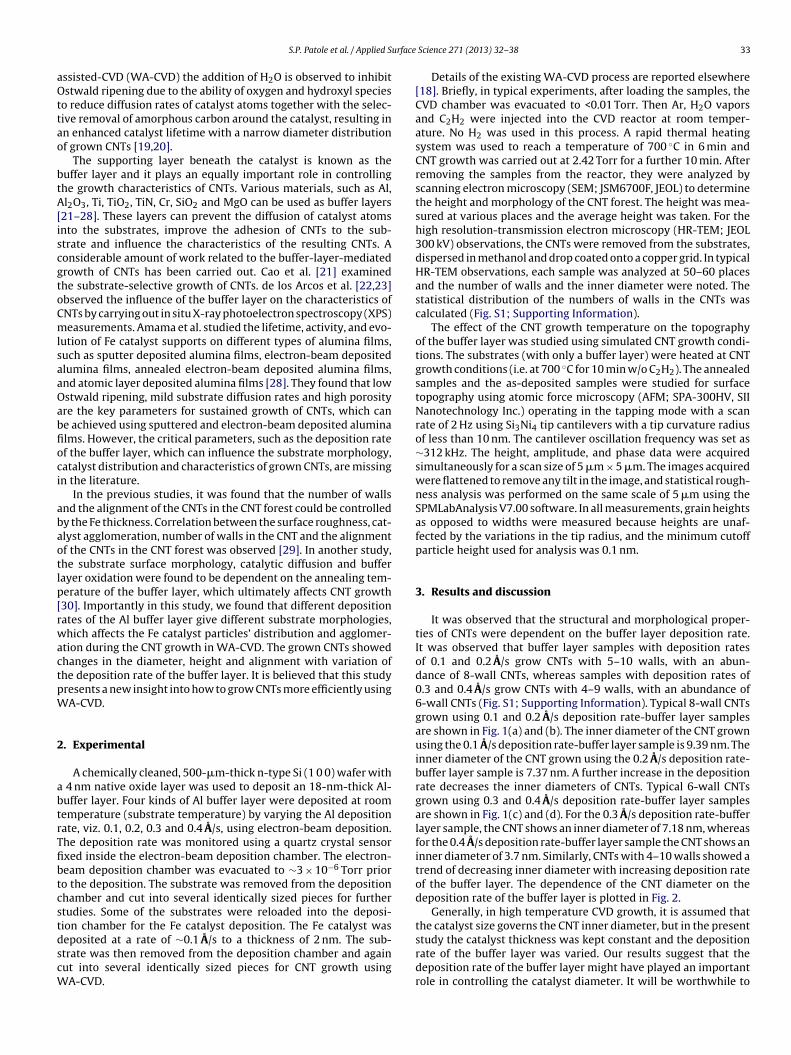
urface
aOttao
btA[iscgtoCmlsaaOabfioci
abaotlp[rwactpW
2
abtrTfibtcstdscW
S.P. Patole et al. / Applied S
ssisted-CVD (WA-CVD) the addition of H2O is observed to inhibitstwald ripening due to the ability of oxygen and hydroxyl species
o reduce diffusion rates of catalyst atoms together with the selec-ive removal of amorphous carbon around the catalyst, resulting inn enhanced catalyst lifetime with a narrow diameter distributionf grown CNTs [19,20].
The supporting layer beneath the catalyst is known as theuffer layer and it plays an equally important role in controllinghe growth characteristics of CNTs. Various materials, such as Al,l2O3, Ti, TiO2, TiN, Cr, SiO2 and MgO can be used as buffer layers
21–28]. These layers can prevent the diffusion of catalyst atomsnto the substrates, improve the adhesion of CNTs to the sub-trate and influence the characteristics of the resulting CNTs. Aonsiderable amount of work related to the buffer-layer-mediatedrowth of CNTs has been carried out. Cao et al. [21] examinedhe substrate-selective growth of CNTs. de los Arcos et al. [22,23]bserved the influence of the buffer layer on the characteristics ofNTs by carrying out in situ X-ray photoelectron spectroscopy (XPS)easurements. Amama et al. studied the lifetime, activity, and evo-
ution of Fe catalyst supports on different types of alumina films,uch as sputter deposited alumina films, electron-beam depositedlumina films, annealed electron-beam deposited alumina films,nd atomic layer deposited alumina films [28]. They found that lowstwald ripening, mild substrate diffusion rates and high porosityre the key parameters for sustained growth of CNTs, which cane achieved using sputtered and electron-beam deposited aluminalms. However, the critical parameters, such as the deposition ratef the buffer layer, which can influence the substrate morphology,atalyst distribution and characteristics of grown CNTs, are missingn the literature.
In the previous studies, it was found that the number of wallsnd the alignment of the CNTs in the CNT forest could be controlledy the Fe thickness. Correlation between the surface roughness, cat-lyst agglomeration, number of walls in the CNT and the alignmentf the CNTs in the CNT forest was observed [29]. In another study,he substrate surface morphology, catalytic diffusion and bufferayer oxidation were found to be dependent on the annealing tem-erature of the buffer layer, which ultimately affects CNT growth30]. Importantly in this study, we found that different depositionates of the Al buffer layer give different substrate morphologies,hich affects the Fe catalyst particles’ distribution and agglomer-
tion during the CNT growth in WA-CVD. The grown CNTs showedhanges in the diameter, height and alignment with variation ofhe deposition rate of the buffer layer. It is believed that this studyresents a new insight into how to grow CNTs more efficiently usingA-CVD.
. Experimental
A chemically cleaned, 500-�m-thick n-type Si (1 0 0) wafer with 4 nm native oxide layer was used to deposit an 18-nm-thick Al-uffer layer. Four kinds of Al buffer layer were deposited at roomemperature (substrate temperature) by varying the Al depositionate, viz. 0.1, 0.2, 0.3 and 0.4 A/s, using electron-beam deposition.he deposition rate was monitored using a quartz crystal sensorxed inside the electron-beam deposition chamber. The electron-eam deposition chamber was evacuated to ∼3 × 10⁻⁶ Torr prioro the deposition. The substrate was removed from the depositionhamber and cut into several identically sized pieces for furthertudies. Some of the substrates were reloaded into the deposi-ion chamber for the Fe catalyst deposition. The Fe catalyst was
eposited at a rate of ∼0.1 A/s to a thickness of 2 nm. The sub-trate was then removed from the deposition chamber and againut into several identically sized pieces for CNT growth usingA-CVD.
Science 271 (2013) 32– 38 33
Details of the existing WA-CVD process are reported elsewhere[18]. Briefly, in typical experiments, after loading the samples, theCVD chamber was evacuated to <0.01 Torr. Then Ar, H2O vaporsand C2H2 were injected into the CVD reactor at room temper-ature. No H2 was used in this process. A rapid thermal heatingsystem was used to reach a temperature of 700 ◦C in 6 min andCNT growth was carried out at 2.42 Torr for a further 10 min. Afterremoving the samples from the reactor, they were analyzed byscanning electron microscopy (SEM; JSM6700F, JEOL) to determinethe height and morphology of the CNT forest. The height was mea-sured at various places and the average height was taken. For thehigh resolution-transmission electron microscopy (HR-TEM; JEOL300 kV) observations, the CNTs were removed from the substrates,dispersed in methanol and drop coated onto a copper grid. In typicalHR-TEM observations, each sample was analyzed at 50–60 placesand the number of walls and the inner diameter were noted. Thestatistical distribution of the numbers of walls in the CNTs wascalculated (Fig. S1; Supporting Information).
The effect of the CNT growth temperature on the topographyof the buffer layer was studied using simulated CNT growth condi-tions. The substrates (with only a buffer layer) were heated at CNTgrowth conditions (i.e. at 700 ◦C for 10 min w/o C2H2). The annealedsamples and the as-deposited samples were studied for surfacetopography using atomic force microscopy (AFM; SPA-300HV, SIINanotechnology Inc.) operating in the tapping mode with a scanrate of 2 Hz using Si3Ni4 tip cantilevers with a tip curvature radiusof less than 10 nm. The cantilever oscillation frequency was set as∼312 kHz. The height, amplitude, and phase data were acquiredsimultaneously for a scan size of 5 �m × 5 �m. The images acquiredwere flattened to remove any tilt in the image, and statistical rough-ness analysis was performed on the same scale of 5 �m using theSPMLabAnalysis V7.00 software. In all measurements, grain heightsas opposed to widths were measured because heights are unaf-fected by the variations in the tip radius, and the minimum cutoffparticle height used for analysis was 0.1 nm.
3. Results and discussion
It was observed that the structural and morphological proper-ties of CNTs were dependent on the buffer layer deposition rate.It was observed that buffer layer samples with deposition ratesof 0.1 and 0.2 A/s grow CNTs with 5–10 walls, with an abun-dance of 8-wall CNTs, whereas samples with deposition rates of0.3 and 0.4 A/s grow CNTs with 4–9 walls, with an abundance of6-wall CNTs (Fig. S1; Supporting Information). Typical 8-wall CNTsgrown using 0.1 and 0.2 A/s deposition rate-buffer layer samplesare shown in Fig. 1(a) and (b). The inner diameter of the CNT grownusing the 0.1 A/s deposition rate-buffer layer sample is 9.39 nm. Theinner diameter of the CNT grown using the 0.2 A/s deposition rate-buffer layer sample is 7.37 nm. A further increase in the depositionrate decreases the inner diameters of CNTs. Typical 6-wall CNTsgrown using 0.3 and 0.4 A/s deposition rate-buffer layer samplesare shown in Fig. 1(c) and (d). For the 0.3 A/s deposition rate-bufferlayer sample, the CNT shows an inner diameter of 7.18 nm, whereasfor the 0.4 A/s deposition rate-buffer layer sample the CNT shows aninner diameter of 3.7 nm. Similarly, CNTs with 4–10 walls showed atrend of decreasing inner diameter with increasing deposition rateof the buffer layer. The dependence of the CNT diameter on thedeposition rate of the buffer layer is plotted in Fig. 2.
Generally, in high temperature CVD growth, it is assumed thatthe catalyst size governs the CNT inner diameter, but in the present
study the catalyst thickness was kept constant and the depositionrate of the buffer layer was varied. Our results suggest that thedeposition rate of the buffer layer might have played an importantrole in controlling the catalyst diameter. It will be worthwhile to
3 urface Science 271 (2013) 32– 38
sodpr01wtFts
CatdottFmrwdgrttC
4 S.P. Patole et al. / Applied S
tudy the morphological properties of the CNT forest before goingn to further detailed discussion. In addition to changes in the inneriameter, CNT height also changed with the deposition rate and islotted in Fig. 2. A CNT forest grown using the 0.1 A/s depositionate-buffer layer sample shows a CNT height of 80 �m, while the.2 A/s deposition rate-buffer layer sample shows a CNT height of25 �m (Fig. S2; Supporting Information). The CNT height increasesith further increase in deposition rate and for the 0.3 A/s deposi-
ion rate-buffer layer sample, a CNT height of 130 �m was observed.urther increases in deposition rate result in the growth of evenaller CNT forests and for the 0.4 A/s deposition rate-buffer layerample, a CNT height of 150 �m was observed.
In order to know more details about the growth process, theNT forest was characterized by SEM at three different places, viz.t the top, middle and bottom of the CNT forest. Fig. 3 showshe SEM images of the CNT forest at these three locations forifferent deposition rate samples. From the overall observationsf the SEM images, we conclude that the overall alignment inhe CNT forest improves with increasing Al deposition rate. Inhe case of the 0.1 A/s deposition rate-buffer layer samples (seeig. 3), the CNTs are strongly misaligned in the CNT forest. Theisaligned CNTs in this sample might have contributed to the
educed height of the CNT forest. Although the catalyst thicknessas fixed at 2 nm, CNTs show more aligned features for 0.4 A/seposition rate-buffer layer samples (see Fig. 3). Overall, in a sin-le CNT forest, from top to bottom, the change in the alignment
evealed that the catalyst particles are not in steady state withhe substrates and are rearranging themselves during the growthime [19]. The catalyst rearrangement is in such a way that theNTs alignment changed with the growth time. However, it wasFig. 1. HR-TEM images of CNTs with different inner diameters, grown using (a
Fig. 2. Effect of buffer layer deposition rate on the inner diameter and height ofCNTs.
observed that CNT growth follows the bottom growth approach,where Fe catalyst particles attach to the substrate and CNTs growvertically from them [18,31]. This suggests that the top portionof the CNT forest grew earlier from the randomly arranged cat-alyst particles while the bottom portion of the CNT forest grewlater from the more arranged/modified catalyst particles. The cat-
˚
alyst rearrangement over a 0.1 A/s deposition rate-buffer layerfavors growth of misaligned CNTs while the catalyst rearrangementover a 0.4 A/s deposition rate-buffer layer favors growth of alignedCNTs.) 0.1, (b) 0.2, (c) 0.3 and (d) 0.4 A/s deposition rate-buffer layer samples.

S.P. Patole et al. / Applied Surface Science 271 (2013) 32– 38 35
F CNT f
fsebuAtiragtdoolot
Fbgtigl
TSw
ig. 3. SEM images showing CNTs morphology at the top, middle and bottom of the
AFM was used to investigate the changes in topographiceatures of buffer layers with varying deposition rates. Fig. 4hows AFM images of as-deposited Al buffer layers with differ-nt deposition rates. The first apparent observation is that theuffer layers are constituted of small grains rather than contin-ous films. Qualitatively, the grain size also increases with thel deposition rate. The observed topographic features revealed
hat although the Al thickness was constant, i.e. 18 nm (as mon-tored from quartz crystal sensor), an increase in the depositionate caused the deposition of bigger grains onto the substratesnd prevented the buffer layer from being uniform and homo-eneous, instead making the surface grainy. It was revealed thathe surface topography of a buffer layer is very sensitive to theeposition rate. Furthermore, to investigate the surface morphol-gy of the substrates at various CNT growth temperatures, somef the Al deposited samples were thermally annealed under simu-ated CNT growth conditions and studied using AFM. The detailsf the thermal annealing are given in the experimental sec-ion.
AFM images of thermally annealed buffer layers are shown inig. 5. Thermal annealing changed the overall topography of theuffer layers. In an apparent observation, we could see that therain size is increased after thermal annealing and the uniformity of
he sample deteriorates with thermal annealing. The overall trendn the grain size suggests that under CNT growth conditions smallrains might have grown into larger grains. We also tried to ana-yze the Fe deposited substrates (data is not shown) but due to theable 1ummary of the physical properties of the different deposition rate buffer layers (as-depoalls with the buffer layer deposition rate.
Buffer layerdeposition (A/s)
Grain mean height (nm) Grain density (1 �m × 1 �m) Averagroughn
As deposited After heating As deposited After heating As dep
0.1 1.9 ± 0.5 3.6 ± 1.1 581 370 0.6
0.2 5.9 ± 1.6 15.4 ± 4.7 542 324 2
0.3 10.4 ± 6.6 25.5 ± 6.6 280 277 4
0.4 12.7 ± 4.1 30.8 ± 8.2 248 169 4.7
orest. The CNTs were grown using the buffer layers with different deposition rates.
limitations of AFM it was difficult to distinguish the buffer layerand catalyst particles.
Furthermore, the previous qualitative discussions are supportedquantitatively by Table 1. The observed topographic features,i.e. root mean square (RMS) values and average feature heights,are given with the Al deposition rate. For simplicity of anal-ysis, the statistical distribution of the feature heights is notconsidered and instead the average feature height is used (seeFig. S3 and Fig. S4; Supporting Information). The RMS values andaverage feature heights show increasing trends with the depositionrate. We also observed an increase in these values after thermaltreatment. For the 0.1 A/s deposition rate-buffer layer sample, theRMS of the as-deposited sample was 0.6 nm and the average fea-ture height was 1.9 nm, which increase after thermal treatment to1.6 and 3.6 nm respectively. For the 0.2 A/s deposition rate-bufferlayer sample, the RMS of the as-deposited sample was 2 nm andthe average feature height was 5.9 nm, which increase after ther-mal treatment to 6.7 and 15.4 nm respectively. Similarly, for the0.3 A/s deposition rate-buffer layer sample, after thermal treatmentthe RMS changed from 4.0 to 7.5 nm and the average feature heightchanged from 10.4 to 25.4 nm. For the 0.4 A/s deposition rate-bufferlayer sample, after thermal treatment the RMS changed from 4.7to 8.7 nm and the average feature height changed from 12.7 to
30.8 nm.In the present study, electron-beam deposition was used todeposit the Al buffer layer. In electron-beam deposition, a graphitecrucible with Al pallets was bombarded with a high kinetic energy
sited and after thermal annealing). Change in CNTs inner diameter and number of
e surfaceess (nm)
CNT inner diameter(nm)
Number of walls in CNT(maximum abundance)
osited After heating
1.6 9.39 ± 0.5 5–10(8)6.7 7.37 ± 0.5 5–10(8)7.5 7.18 ± 0.5 4–9(6)8.7 3.7 ± 1 4–9(6)

36 S.P. Patole et al. / Applied Surface Science 271 (2013) 32– 38
F(
eoAipseib(tmgfli
Fig. 5. AFM topography images showing the thermally annealed buffer layers with
ig. 4. AFM topography images showing the as-deposited buffer layers with (a) 0.1,b) 0.2, (c) 0.3 and (d) 0.4 A/s deposition rates.
lectron beam. Upon incident with the crucible, the kinetic energyf electron beam is converted into thermal energy, which heats thel pallet and results in its melting. An increase in e-beam current
ncreases the deposition rate (the amount of material depositeder unit time; unit: A/s) which was monitored by a quartz crystalensor. It is suggested that the flux, i.e. the number of Al adatomsvaporated per unit time and per unit area, increases with thencrease in electron-beam current. The increase in deposition rate,asically, provides more Al adatoms to seat on the Si substratewhich was at room temperature) per unit time. After seating onhe Si substrate, thermodynamically unfavorable Al adatoms try to
inimize their surface energy and form thermodynamically stablerains. The final grain size eventually depends on the incident Alux which results from the deposition rate. Therefore, with increas-
ng deposition rate, bigger grains with greater feature heights are
(a) 0.1, (b) 0.2, (c) 0.3 and (d) 0.4 A/s deposition rates. Thermal annealing was carriedout in the simulated CNT growth conditions.
observed. A summary of the physical properties of different depo-sition rate-buffer layers is given in Table 1.
The increase in the RMS and feature heights roughens the sur-face and gives more porosity to the substrate. Higher porosityof the substrate provides a greater supply of feed stock gases tothe catalyst [28,32]. In WA-CVD, feed stock gases contain oxygenand hydroxyl species which have a special ability to reduce thediffusion or migration rates of catalyst atoms from one catalyst toanother across the sample substrates. Previously it was observedthat during CNT growth, oxygen and hydroxyl radicals attach tothe Al buffer layer and prevent Fe particles from Ostwald ripening[19]. The higher feed stock supply at the catalyst protects it from
Ostwald ripening and might have contributed to the small size ofcatalyst particles for higher deposition rate buffer layers. Contrary,for lower deposition rate buffer layers with less porosity, the lower
S.P. Patole et al. / Applied Surface Science 271 (2013) 32– 38 37
Fig. 6. Schematic illustration of Al grain size variation on (a) as-deposited buffer layers and on (b) thermally annealed buffer layers with different deposition rates. (c) TheFe catalyst deposited onto the buffer layers (d) undergoes modifications at the CNT growth conditions and gives large diameter, low density catalyst particles for small Alg
ftct
Cdddaiatdnttsttgt(tollotFt
rains and small diameter catalyst particles with higher density for large Al grains.
eed stock supply allows more Ostwald ripening of the catalyst par-icles, which might have contributed to the large diameter of theatalyst particles. The change in the catalyst diameter also changeshe diameter of the CNTs.
The effects of Al grain size and average Al feature height onNT diameter are illustrated in Fig. 6. In Fig. 6(a), the effect of Aleposition rate on the Al grain size is depicted. The increase in Aleposition rate increases the Al grain size (refer Fig. 4, it gives evi-ence that with deposition rate Al grain size grows larger), whichlso increases the average Al feature height. Thermal annealingncreases the overall Al grain size (refer Fig. 5, it gives evidence thatfter thermal annealing Al grain size grows larger), which increaseshe average Al feature height (see Fig. 6(b)). Similarly, substrateseposited with Fe catalyst (Fig. 6(c)) follow the same trend butow the Fe particles come into the picture (see Fig. S5; Suppor-ing Information). The surface area for large Al grains is greaterhan that for small Al grains. Therefore, the increased Al grainize accommodates more Fe catalyst per Al grain (Fig. 6(c)). Underhe CNT growth conditions, Fe-catalyst particles giving seed tohe CNT growth (Fig. 6(d)). Similarly, at the beginning of the CNTrowth, Ostwald ripening/rearrangement of small Fe catalyst par-icles seated on the Al grains forms the seeds for CNT growthFig. 6(d)) [19,20]. The surface area for large Al grains is greater thanhat for the small Al grains. Therefore, the resultant rearrangementf Fe catalyst particles form smaller Fe catalyst seeds onto thearge Al-grains. Similarly, smaller Al grains form larger Fe cata-yst seeds. If we assume that the CNT inner diameter is dependent
n the Fe catalyst diameter [14], then the resultant CNT will havehe same diameter as the Fe catalyst seed (which was observed inig. 1). Moreover, the change in the catalyst diameter gives riseo size dependent catalyst activity and at a given fixed amountof feed stock it contributes a different CNT yield [33], which wasapparent as a change in CNT height and number of walls (seeFigs. S1 and S2; Supporting Information). Large diameter catalystsconsume more feed stock and grow CNTs with higher number ofwalls. Comparatively small diameter catalysts consume less feed-stock and grow CNTs with less number of walls. Thus, the observeddecrease in the CNT diameter (Fig. 1), decrease in the CNT walls andincrease in the CNT height with increasing Al-deposition rate can beunderstood.
4. Conclusions
The effect of Al buffer layer deposition conditions on the mor-phological and structural properties of CNTs has been investigated.Buffer layer deposition controls the surface morphology of the sub-strate onto which the Fe catalyst particles are seated. At lowerdeposition rates, the buffer layer forms small grains and small fea-ture heights. On the other hand, at higher deposition rates, thebuffer layer forms larger grains and larger feature heights. Smallgrains are responsible for large catalyst agglomerates and lowerfeedstock supply, which in turn lead to the growth of large diam-eter and misaligned CNTs. In contrast, large grains are responsiblefor small catalyst agglomerates and higher feedstock supply, whichin turn result in the growth of small diameter and aligned CNTs.Our findings elucidate the effect of buffer layer deposition on thecharacteristics of CNTs.
Acknowledgments
This study was supported by Samsung Advanced Institute ofTechnology (SAIT) and Basic Science Research Program through
3 urface
tMTpbg
A
fa
R
[
[
[
[
[
[[
[
[[
[
[
[
[
[
[[
[
[
[
[
[
8 S.P. Patole et al. / Applied S
he National Research Foundation of Korea (NRF) funded by theinistry of Education, Science and Technology (2011-0006268).
his work was partly supported by the GRRC program of Gyeonggirovince [(GRRC Sungkyunkwan 2010-B10), Development of Car-on nano composite material for lightweight vehicle]. S.P.P. israteful to the Korean Government for the BK-21 fellowship.
ppendix A. Supplementary data
Supplementary data associated with this article can beound, in the online version, at http://dx.doi.org/10.1016/j.psusc.2012.12.129.
eferences
[1] M. Zhang, K.R. Atkinson, R.H. Baughman, Science 306 (2004) 1358–1361.[2] M.D. Lima, S. Fang, X. Lepro, C. Lewis, R. Ovalle-Robles, J. Carretero-Gonzalez,
E. Castillo-Martínez, M.E. Kozlov, J. Oh, N. Rawat, C.S. Haines, M.H. Haque,V. Aare, S. Stoughton, A.A. Zakhidov, R.H. Baughman, Science 331 (2011)51–55.
[3] J. Foroughi, G.M. Spinks, G.G. Wallace, J. Oh, M.E. Kozlov, S. Fang, T. Mir-fakhrai, J.D.W. Madden, M.K. Shin, S.J. Kim, R.H. Baughman, Science 334 (2011)494–497.
[4] N.P. Lopez, B. Rebollo-Plata, J.A. Briones-Leon, A. Morelos-Gomez, D.Hernandez-Cruz, G.A. Hirata, V. Meunier, A.R. Botello-Mendez, J.C. Charlier, B.Maruyama, E. Munoz-Sandoval, F. Lopez-Urias, M. Terrones, H. Terrones, ACSNano 5 (2011) 5072–5077.
[5] M. Xu, D.N. Futaba, T. Yamada, M. Yumura, K. Hata, Science 330 (2011)1364–1368.
[6] H. Kataura, Y. Kumazawa, Y. Maniwa, Y. Ohtsuka, R. Sen, S. Suzuki, Y. Achiba,Carbon 38 (2000) 1691–1697.
[7] R.H. Hauge, C.L. Pint, S.T. Pheasant, A.N.G. Parra-Vasquez, C.Horton, Y.Q. Xu, Journal of Physical Chemistry C 113 (2009)4125–4133.
[8] G. Eres, A.A. Kinkhabwala, H.T. Cui, D.B. Geohegan, A.A. Puretzky, D.H. Lowndes,
Journal of Physical Chemistry B 109 (2005) 16684–16694.[9] T. Saito, S. Ohshima, T. Okazaki, S. Ohmori, M. Yumura, S. Iijima, Journal ofNanoscience and Nanotechnology 8 (2008) 6153–6157.
10] R. Xiang, E. Einarsson, J. Okawa, Y. Miyauchi, S. Maruyama, Journal of PhysicalChemistry C 113 (2009) 7511–7515.
[
[
Science 271 (2013) 32– 38
11] A.R. Harutyunyan, G.G. Chen, T.M. Paronyan, E.M. Pigos, O.A. Kuznetsov, K.Hewaparakrama, S.M. Kim, D. Zakharov, E.A. Stach, G.U. Sumanasekera, Science326 (2009) 116–120.
12] B.G. Sumpter, V. Meunier, J.M. Romo-Herrera, E. Cruz-Silva, D.A. Cullen, H. Ter-rones, D.J. Smith, M. Terrones, ACS Nano 1 (2007) 369–375.
13] H. Liu, G. Cheng, R. Zheng, Y. Zhao, C. Liang, Surface and Coatings Technology202 (2008) 3157–3163.
14] C.L. Cheung, A. Kurtz, H. Park, C.M. Lieber, Journal of Physical Chemistry B 106(2002) 2429–2433.
15] C. Lu, J. Liu, Journal of Physical Chemistry B 110 (2006) 20254–20257.16] M.G. Hahm, Y.K. Kwon, E. Lee, C.W. Ahn, Y.J. Jung, Journal of Physical Chemistry
C 11 (2008) 17143–17147.17] S.P. Patole, P.S. Alegaonkar, J.H. Lee, J.B. Yoo, Europhysics Letters 81 (2008),
38002-1–38002-6.18] S.P. Patole, P.S. Alegaonkar, H.C. Lee, J.B. Yoo, Carbon 46 (2008) 1987–1993.19] P.B. Amama, C.L. Pint, L. McJilton, S.M. Kim, E.A. Stach, P.T. Murray, R.H. Hauge,
B. Maruyama, Nano Letters 9 (2009) 44–49.20] T. Yamada, A. Maigne, M. Yudasaka, K. Mizuno, D.N. Futaba, M. Yumura, S. Iijima,
K. Hata, Nano Letters 8 (2008) 4288–4292.21] A. Cao, P.M. Ajayan, G. Ramanath, R. Baskaran, K. Turner, Applied Physics Letters
84 (2004) 109–111.22] T. de los Arcos, M.G. Garnier, J.W. Seo, P. Oelhafen, V. Thommen, D.J. Mathys,
Journal of Physical Chemistry B 108 (2004) 7728–7734.23] T. de los Arcos, M.G. Garnier, P. Oelhafen, D. Mathys, J.W. Seo, C. Domingo, J.V.
Garcia-Ramos, S. Sanchez-Cortes, Carbon 42 (2004) 187–190.24] T. de los Acros, Z.M. Wu, P. Oelhafen, Chemical Physics Letters 380 (2003)
419–423.25] G.Y. Xiong, D.Z. Wang, Z.F. Ren, Carbon 44 (2006) 969–973.26] C.C. Chiu, T.Y. Tsai, N.H. Tai, C.Y. Lee, Surface and Coatings Technology 200
(2006) 3215–3219.27] H.C. Lee, P.S. Alegaonkar, D.Y. Kim, H.H. Lee, T.Y. Lee, S.Y. Jeon, J.B. Yoo, Thin
Solid Films 516 (2008) 3646–3650.28] P.B. Amama, C.L. Pint, S.M. Kim, L. McJilton, K.G. Eyink, E.A. Stach, R.H. Hauge,
B. Maruyama, ACS Nano 4 (2010) 895–904.29] S.P. Patole, P.S. Alegaonkar, H.C. Shin, J.B. Yoo, Journal of Physics D: Applied
Physics 41 (2008) 155311–155321.30] S.P. Patole, S.M. Yu, D.W. Shin, H.J. Kim, K.W. Kwon, J.B. Yoo, Journal of Physics
D: Applied Physics 43 (2010) 95304–95311.31] S.P. Patole, J.H. Park, T.Y. Lee, J.H. Lee, A.S. Patole, J.B. Yoo, Applied Physics Letters
93 (2008) 114101–114111.32] F. Shoushan, G.C. Michael, R.E. Nathan, W.T. Thomas, M.C. Alan, D. Hongjie,
Science 283 (1999) 512–514.33] S.P. Patole, H. Kim, J. Choi, Y. Kim, S. Baik, J.B. Yoo, Applied Physics Letters 96
(2010), 094101-1–094101-3.


![Applied Surface Sciencenpt.pusan.ac.kr/sites/npt/download/[53]ASS-2017.pdf · 2018-03-28 · Applied Surface Science 415 (2017) 149–154 Contents lists available at ScienceDirect](https://static.fdocuments.us/doc/165x107/5f036c897e708231d4092331/applied-surface-53ass-2017pdf-2018-03-28-applied-surface-science-415-2017.jpg)