Applications of Optical Frequency Shift Keying Modulation ... · Optical frequency-shift keying...
75
f “ / ij / I— ; — J Applications of Optical Frequency Shift Keying Modulation Format in Optical Networks DENG NING A Thesis Submitted in Partial Fulfilment of the Requirements for the Degree of Master of Philosophy in Information Engineering © The Chinese University of Hong Kong August 2004 The Chinese University of Hong Kong holds the copyright of this thesis. Any person(s) intending to use a part or whole of the materials in the thesis in a proposed publication must seek copyright release from the Dean of Graduate School
Transcript of Applications of Optical Frequency Shift Keying Modulation ... · Optical frequency-shift keying...

f “ / i j /
I— ; — J
Applications of Optical Frequency
Shift Keying Modulation Format in
Optical Networks
DENG NING
A Thesis Submitted in Partial Fulfilment
of the Requirements for the Degree of
Master of Philosophy
in
Information Engineering
© The Chinese University of Hong Kong
August 2004
The Chinese University of Hong Kong holds the copyright of this thesis. Any person(s) intending to use a part or whole of the materials in the thesis in a proposed
publication must seek copyright release from the Dean of Graduate School

々 / 统 系 ‘ 書 囷 ^ ^
( l 0 9 m M5 j l j UNIVERSITY / M
NgffisaiBRARY SYSTEMy>^

ii
Acknowledgement
I would like to thank everybody who has contributed in diverse ways, great or small,
to my ideas and work in the past two years. First and foremost, I proclaim my most
heartfelt gratitude to my thesis supervisor, Professor Calvin Chun-Kit Chan in the
Department of Information Engineering, the Chinese University of Hong Kong.
Professor Chan's diligence, tenacity, ingenuity and agility are of great help to promote
the formation of the research attitude and methodology of a neophyte Master student
like me.
Great thanks must also present to Professor Lian-Kuan Chen and Professor Chinlon
Lin in the Department of Information Engineering. Illuminative discussions with them
have brought me into wider and deeper research perspectives in photonics. In addition,
I would like to thank Professor Frank Tong and Professor K. W . Cheung, also the
faculty members in the Lightwave Communications Laboratory, for their support and
guidance in the Laboratory.
In the past two years studying in the Lightwave Communications Laboratory in the
Department of Information Engineering, I was very pleased to have collaborated with
and accepted aids from all Lab members. I would like to show m y most sincere thanks
to the current members - Mr. Guowei Lu, Mr. Zhaoxin Wang, Mr. Yuen-Ching Ku,
Mr. Chi-Man Lee, Mr. Jian Zhao, Mr. Clement Cheung, Mr. Siu-Ting Ho, Mr.
Xiaofeng Sun, Mr. Siu-San Pun and those who have graduated — Dr. Kit Chan, Dr.
Vincent Hung’ Ms. Yu Zhang, Mr. Jimmy Chan, Mr. Jordan Tse, Ms. Yi Yang and Mr.
Scott Tarn.
Last but not the least, I would like to give great debt of gratitude to m y family for their
perdurable siistainment and tolerance. Special thanks are owed to a lot of friends of
mine who made the hard times easier during the past few years.

Hi
Abstract
Optical frequency-shift keying (FSK), as an attractive constant-intensity modulation
format, has recently aroused much research attention. It has been found to have
enhanced tolerance against fiber nonlinearities in optical signal transmission and to
offer better flexibility in optical signal processing. In this thesis, we propose and
investigate several system applications of optical FSK format in optical access
networks as well as optical label switching (OLS) networks.
In the arena of optical access networks, wavelength division multiplexing passive
optical network ( W D M - P O N ) is a promising technology to deliver high-speed data
traffic. Among various W D M - P O N architectures, the one utilizing centralized light
sources (CLS) is the most attractive as it does not require any wavelength-registered
optical sources at the optical network unit (ONU) side, thus greatly relaxes the
requirement of wavelength management. In this thesis, we propose to employ optical
FSK as the downstream modulation format, to facilitate the re-modulation for the
upstream traffic at the O N U . Moreover, different implementations of the optical FSK
transmitter have been investigated for this application. Besides, a novel optical FSK
transmitter, which is based on an optical phase modulator and an optical delay
interferometer, is proposed and characterized. Various system design issues and
experimental investigations on the system performance will be discussed.
Optical label switching is an attractive approach to support low-latency and efficient
packet routing and forwarding for future high-speed optical packet networks. In this
thesis, we propose a new type of orthogonal labelling scheme by employing FSK
modulation format for the high-speed optical packet payload. The relatively low-speed
label is intensity modulated onto the high-speed constant-intensity payload, thus the
amplitude-shift keying (ASK) modulated label is orthogonal to the FSK modulated
payload. Moreover, a novel scheme of all-optical label swapping is also proposed to
extract and erase the old label before a new label is inserted. Besides, we further
investigate the orthogonal labelling and all-optical label swapping schemes by using

iv
optical differential phase shift keying (DPSK), which is another kind of constant-
intensity modulation format.
In addition, we have characterized the receiver performance of such optical ASK/FSK
and ASK/DPSK orthogonal signals. Receiver sensitivities of ASK, FSK, D P S K data
in such ASK/FSK, ASK/DPSK signals have been analytically and numerically
computed, with respect to different signal bit rates and extinction ratios of the A S K
data signal. W e have also carried out experimental measurements to validate the
theoretical analysis.

V
摘要
近年來,一種強度恆定的光調製方式一一頻移鍵控(FSK)引起了很多研究者
的注意。研究者們發現使用FSK光調製方式的光信號在傳輸中可以抵抗光纖非
錢性的影響,同時也為更靈活的光信號處理提供了可能。本篇論文將提出和研
究FSK光調製方式在若干光系統中的幾種應用,這些光系統包括光接入網絡和
光標簽交換網絡等等。
在光接入網領域,波分复用無源光網絡( W D M - P O N )在提供高速數據流方面
有著廣 _的前景。在各種 W D M - P O N的的體系結構中,集中光源式結構在光網
絡單元(ONU)処省去了任何需要登記波長的光源,所以放寬了對波長管理的
需求,因而是一種最具吸引力的結構。我們在這篇論文中提出用FSK作爲下行
信号的光調製方式來促進在ONU對上行數據的再調製。此外,在這項研究中我
們考察了幾種不同的FSK發射机,包括我們最新提出的一種基於光相位調製的
發射机。我們對這樣的光接入網系統設計重心和性能進行了實驗的研究。
光標記交換是一種在未來光包交換網絡中支持為低延時而高效的路由轉發而設
計的一種新技術。本篇論文將提出一種新的正交標記方案來實現這種技術。我
們提出的方案使用幅移鏈控(ASK)的光信號作爲標記正交的調製在FSK格式
的淨荷之上。此外,本文亦提出一種新的標記交換方法來實現舊標簽的去除及
更新。爲了進一步驗證這禪標簽方案及標簽交換方法的有效性,我們還通過實
驗考察了光差分相移鍵控(DPSK)作爲淨荷調製方式的情況。
最後,我們分析了用在標記交換網的這種正交調製方式( A S K / F S K,
ASK/DPSK)的接收機性能。我們通過解析和數值的方法計算了這種正交調製
信號中的 A S K, F S K , DPSK败據的接收機性能,從而清晰描述了接收機靈敏
度与ASK信號消光比、比特率之間的關係。另外我們也通過實驗測量來驗證了
理論分析模型。

vi
Table of Contents
ABSTRACT iii
^ V
1 BACKGROUND AND INTRODUCTION 1
1.1 OPTICAL FRHQUIZNCY-SHIFT KEYING (FSK) 1
1.1.1 Basic concepts and research hotspots of optical F S K 1
1.1.2 Optical F S K Transmitter and Receiver 3
1.2 WAVEL上NGTI I DIVISION MULTIPLEXING OPTICAL PASSIVE N E T W O R K S 8
1.3 OPTICAL LABHL SWITCHING (〇LS) N E T W O R K S I o
1.4 TI IHSIS CONTRIBU TION A N D ORGANIZATION 11
2 DATA RE-MODULATION ON DOWNSTREAM OPTICAL FSK SIGNALS IN
WDM-PONS 12
2.1 O V H R V M W OF RLILATED W O R K S 12
2.2 P O N ARCIHTHCTIJRI:: USING DOWNSTRL-AM OPTICAL F S K SIGNALS 13
2.3 C L S P O N DliMONSTRA TlON USING THREE DIFFERENT OPTICAL F S K TRANSMITTERS ... 14
2.3.1 With an optical FSK. transmitter based on direct modulation in a D F B laser 14
2.3.2 With an optical F S K transmitter based on complementary intensity modulation.... 17
2.3.3 Willi our proposed optical F S K transmitter based on phase modulation 21
2.4 SYS TEM PERFORMANCE BY USING PHASE M O D U L A T I O N BASED F S K TRANSMITTER……26

vii
2.4.1 Wavelength detune of light sources 27
2.4.2 Detune of the DI frequency response 29
2.4.3 Dispersion tolerance 30
2.5 S U M M A R Y 32
3 INTENSITY-MODULATED LABELLING ON OPTICAL FSK OR DPSK
PAYLOADS 丨N OLS NETWORKS 34
3.1 EXISTING LABELLING Sci-iriMES A N D THEIR FEATURES 34
3.1.1 Bit serial labelling 35
3.1.2 Subcarrier multiplexed ( S C M ) labelling 36
3.1.3 Orthogonally modulated labelling 37
3.2 TI III PROPOSIID 0 0 K LABELLING SCHEME A N D O L S SYSTEM ARCHITECTURE 38
3.3 AI丄-OPTICAL LAI3I:;L SWAPPING A N D OTHER CRITICAL ISSUES 39
3.4 SYSTHM DHMONSTRATION 40
3.5 S U M M A R Y 45
4 PERFORMANCE CHARACTERIZATION OF THE ASK/FSK AND ASK/DPSK
ORTHOGONAL SIGNALS 46
4.1 INTRODUCTION A N D FORMULATION 46
4.2 TIITIORIITICAL ANALYSIS 48
4.2.1 Optical A S K performance in orthogonal signals 48
4.2.2 Optical F S K performance in A S K / F S K signals 49

viii
4.2.3 Optical D P S K performance in A S K / D P S K signals 51
4.3 ANALYTICAL A N D EXPERIMENTAL RESULTS 55
4.4 CONCLUSION 57
5 SUMMARY 58
5.1 THESIS S U M M A R Y 58
5.2 FUTURI:; WORK 59
LIST OF PUBLICATIONS 61
REFERENCES 62
BACKGROUND AND INTRODUCTION 1
1 Background and Introduction
1.1 Optical Frequency-Shift Keying (FSK)
1.1.1 Basic concepts and research hotspots of optical FSK
In optical digital communication systems, the representation of information is
generally realized by modulating the amplitude, or the frequency, or the phase of a
lightwave carrier. In the case of frequency modulation, information is coded on the
optical carrier by shifting its carrier frequency, which is known as optical frequency-
shift keying (FSK) [1]. In a binary system, mark (“1”)or space ("0") information is
represented by the positive or negative frequency deviation of the frequency-shifted
optical carrier. The scalar field of a FSK signal can be written as
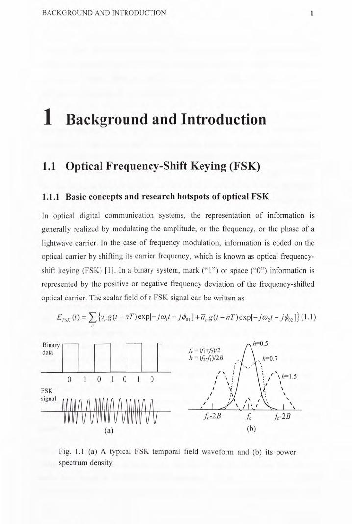
( 0 = X {““射 ‘一 - ] + a „ g { t — n T ) Q x p l - J c o , t — ]} (1.1) n
Binary 广 八/7 二 0.5
data . / : = 請 2 \ h - U i - m B J V h = O J
0 1 0 1 0 1 0 ,、、、;/ V/、、,丨.5
FSK / i W �� 一 _ 薩 瞧 _ , / 丨 力 、 / I
(a) (b)
Fig. 1.1 (a) A typical FSK temporal field waveform and (b) its power
spectrum density

B A C K G R O U N D A N D INTRODUCTION 2
where a^ is the bit information (either 1 or 0), o)\ and coi are the respective carriers'
angular frequencies, g{t) is the signal baseband waveform which is ideally a
rectangular window function, and 如,(jxn are the initial phase values, for the
lightwave carriers with co\, coi, respectively.
The total bandwidth of a FSK signal is approximately 2^+A/, where A/ is the
frequency spacing, i.e.. A/ =l/i:/2|, while B is the signal bit rate. Fig. 1.1(a) shows a
typical FSK temporal field and its corresponding baseband signal waveform, while
Fig. 1.1(b) sketches the FSK power spectra with different frequency spacings. When
A f - < B , the bandwidth approaches A/' and is nearly independent of the signal bit rate;
the FSK signal in this case is commonly known as wideband FSK. On the other hand,
if A/'、!3, the FSK signal is known as narrowband FSK, with the bandwidth being
determined mainly by 2B. Optical FSK signals generated from different optical FSK
transmitters may have different ranges of bandwidth, depending on their physical
features. The choice of the FSK signal bandwidth is affected by both the
communication channel bandwidth and the scalability of the incorporated FSK
transmitter/detector.
In recent years, researchers have focused a lot of enthusiasm on seeking for the best
optical modulation format in long-haul or intermediate-distance transmission. Besides
the attention paid on optical amplitude-shift keying (ASK, a.k.a. on-off keying) format
and its various derivatives, angle modulation formats such as differential phase-shift
keying (DPSK) and FSK have also been considered as the suitable alternatives. Some
good results on optical FSK signal transmission have been achieved. In [2], a 10-Gb/s
FSK signal being transmitted over 160 km with balanced detection outperformed
D P S K and A S K signals by its best receiver sensitivity. However, the optical FSK
format has some drawbacks. For instance, wideband FSK is more sensitive to fiber
dispersion than other formats and thus may suffer from larger dispersion induced
penalty.
Other than high-speed transmission, optical FSK format can also be employed to
bolster flexible functions in optical networks. In [3], optical FSK format was used to
assist data control in S T A R N E T W D M networks. The payload data was coded in
optical FSK format on the optical carrier that also carried control information in
B A C K G R O U N D A N D INTRODUCTION 3
optical A S K format simultaneously. In this way, two separable orthogonal sets of data
co-existed in one wavelength channel. Another application is addressed in optical
packet networks. The high-speed payload was carried by optical A S K (intensity-
modulated) data and the relatively low-speed label was transmitted on the same
optical carrier with FSK modulation [4]. In Chapter 3, we will propose an alternative
approach to implement labelling function in optical packet networks.
1.1,2 Optical FSK Transmitter and Receiver
The several prevailing methods to generate an optical FSK signal have their respective
advantages and limitations. In this section, we summarize the main characteristics of
several distinct optical FSK transmitters, which beget different considerations in
different system applications.
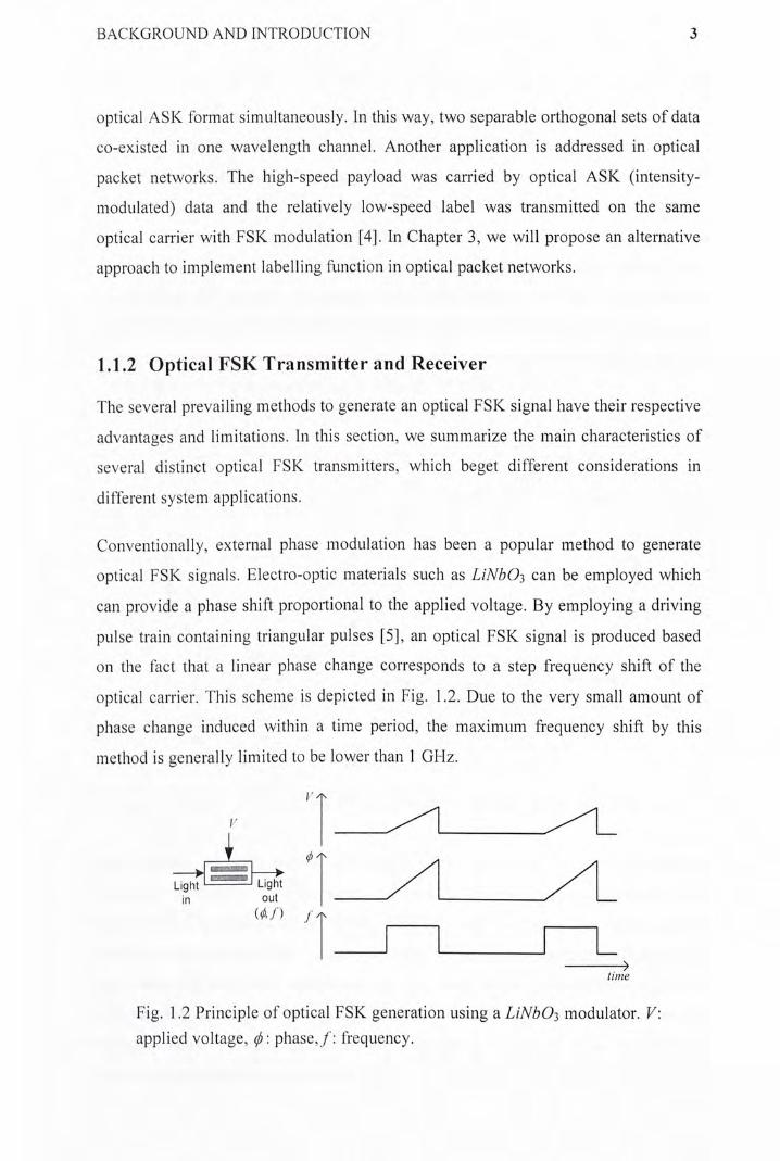
Conventionally, external phase modulation has been a popular method to generate
optical FSK signals. Electro-optic materials such as L i N b O i can be employed which
can provide a phase shift proportional to the applied voltage. By employing a driving
pulse train containing triangular pulses [5], an optical FSK signal is produced based
on the fact that a linear phase change corresponds to a step frequency shift of the
optical carrier. This scheme is depicted in Fig. 1.2. Due to the very small amount of
phase change induced within a time period, the maximum frequency shift by this
method is generally limited to be lower than 1 GHz.
I’八
丄 ! ^ — — ^
Ligh「l Light y / ^
in out , Z _
( 灯 ) f 八
lime
Fig. 1.2 Principle of optical FSK generation using a LiNbO�modulator. V: applied voltage,小,.phase,/: frequency.
B A C K G R O U N D A N D INTRODUCT ION 4
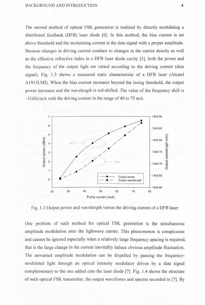
The second method of optical FSK generation is realized by directly modulating a
distributed feedback (DFB) laser diode [6]. In this method, the bias current is set
above threshold and the modulating current is the data signal with a proper amplitude.
Because changes in driving current conduce to changes in the carrier density as well
as the effective refractive index in a D F B laser diode cavity [5], both the power and
the frequency of the output light are varied according to the driving current (data
signal). Fig. 1.3 shows a measured static characteristic of a D F B laser (Alcatel
A1915LM1). When the bias current increases beyond the lasing threshold, the output
power increases and the wavelength is red-shifted. The value of the frequency shift is
〜IGHz/mA with the driving current in the range of 40 to 75 m A .
7 n r 1545 .90
6 -
/ - 1545.85
? - ^ ^ 声 Z E
§ 3 - / / - 1545.75 1
a Z / ro 3 / - >.〜•、、 I B- 2 - / [ X - 4 . . - — — 3 ^ / - 1545.70 Q-〇 / Z — a
1- / , , z o
J ^ • Output power “ 1545.65
0 - » — Output wavelength
I 1 1 1 1 1- 1545.60
20 3 0 4 0 50 6 0 7 0 80
P u m p current (mA)
Fig. 1.3 Output power and wavelength versus the driving current of a D F B laser
One problem of such method for optical FSK generation is the simultaneous
amplitude modulation onto the lightwave carrier. This phenomenon is conspicuous
and cannot be ignored especially when a relatively large frequency spacing is required,
that is the large change in the current inevitably induce obvious amplitude fluctuation.
The unwanted amplitude modulation can be dispelled by passing the frequency-
modulated light through an optical intensity modulator driven by a data signal
complementary to the one added onto the laser diode [7]. Fig. 1.4 shows the structure
of such optical FSK transmitter, the output waveforms and spectra recorded in [7]. By

B A C K G R O U N D A N D INTRODUCT ION 5
using this kind of transmitter based on direct modulation of D F B laser diodes, the
carrier phase varies continuously from bit to bit, which is referred to as continuous-
phase FSK (CPFSK). A limitation of this method is that the operating bit rate is
restrained up to 2.5 Gb/s unless D F B laser diodes with special designs are exploited
[4].
Data Generator ^ S X l zero Icvc丨 zero level
• I • r M * • I I 500 ps/div N k 500 ps/div Electrical Delay 化、
Data Data f ) ⑷ ⑶ I V w / j ‘ 1 _ 一 j I mnom EA conv*nuU«
: : A ' '
•-vw^ Biasl ^ wvw- Bias2 |.,。 ^
' D F B [ e a ^ ] y 爱: J • •• V '"»U ISHIt <SU» isu.n ISSSOO lUSOl lUS lI 1US» <SUJ!
Wavitooyt) (ran) (C)
Fig. 1.4 Optical FSK transmitter configuration using direct modulation,
and the output waveforms and spectra (after Ref. [7]).
From the definition of Eq. (1.1), an optical FSK signal can also be deemed as the
combination of two wavelength carriers, each modulated by a complementary
electrical data signal. This illuminates us that an optical FSK transmitter can be
obtained using a structure shown in Fig. 1.5. Two continuous-wave (CW) light at
different frequencies (wavelengths) are fed into two optical intensity modulators,
driven by the electrical data signal and its complementarity, respectively. High-speed
operation can be achieved by such external modulation at the expense of increased
complexity. Also, the two complementary data signals have to be synchronized by
using tunable electrical delay lines.
DF已 1 I external modulator f ^ A
D A T A — ~ \ FSK — 丽 」 迎 : 丨 a y 50:5”⑶丁
~ d F B 2 1 - 一丨
货 modulator
Fig. 1.5 Optical FSK transmitter based on complementary intensity modulation
B A C K G R O U N D A N D INTRODUCTION 6
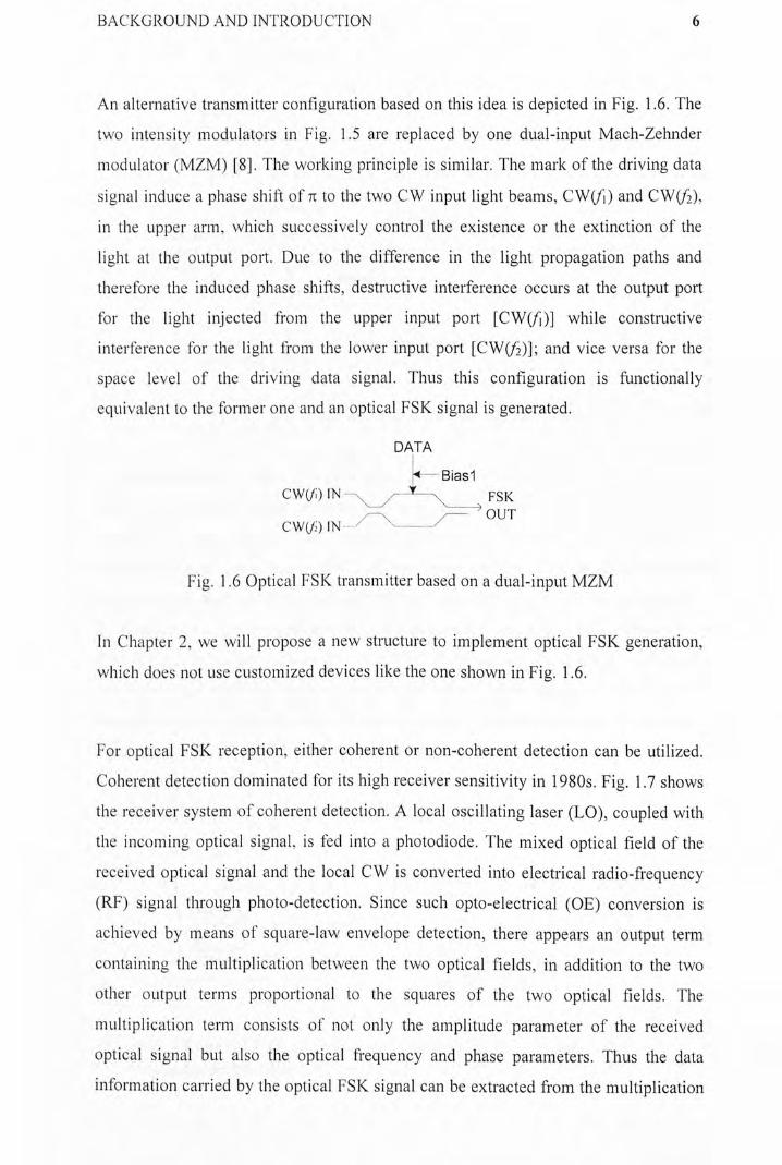
An alternative transmitter configuration based on this idea is depicted in Fig. 1.6. The
two intensity modulators in Fig. 1.5 are replaced by one dual-input Mach-Zehnder
modulator ( M Z M ) [8]. The working principle is similar. The mark of the driving data
signal induce a phase shift of ti to the two C W input light beams, CW(/i) and CW(/2),
in the upper arm, which successively control the existence or the extinction of the
light at the output port. Due to the difference in the light propagation paths and
therefore the induced phase shifts, destructive interference occurs at the output port
for the light injected from the upper input port [CW(/i)] while constructive
interference for the light from the lower input port [CW(/2)]; and vice versa for the
space level of the driving data signal. Thus this configuration is functionally
equivalent to the former one and an optical FSK signal is generated.
DATA
Bias1 CW(/i) I N - _ _ FSK
CW(/2) IN \ Z
Fig. 1.6 Optical FSK transmitter based on a dual-input M Z M
In Chapter 2, we will propose a new structure to implement optical FSK generation,
which does not use customized devices like the one shown in Fig. 1.6.
For optical FSK reception, either coherent or non-coherent detection can be utilized.
Coherent detection dominated for its high receiver sensitivity in 1980s. Fig. 1.7 shows
the receiver system of coherent detection. A local oscillating laser (LO), coupled with
the incoming optical signal, is fed into a photodiode. The mixed optical field of the
received optical signal and the local C W is converted into electrical radio-frequency
(RF) signal through photo-detection. Since such opto-electrical (OE) conversion is
achieved by means of square-law envelope detection, there appears an output term
containing the multiplication between the two optical fields, in addition to the two
other output terms proportional to the squares of the two optical fields. The
multiplication term consists of not only the amplitude parameter of the received
optical signal but also the optical frequency and phase parameters. Thus the data
information carried by the optical FSK signal can be extracted from the multiplication

B A C K G R O U N D A N D INTRODUCTION 7
term of the output electrical RF signal. Relying on whether the carrier frequencies of
received optical signal and LO are the same or not, two approaches namely homodyne
and heterodyne coherent detection have been proposed [5].
Polarization . Decision „ . � beam splitter , P ‘旧「 circuit Received I , i ^ r ~ optical、⑴• \ ——)〉~> (-dyne) | ) signal ^ ^ ——^^ ! ^ ! 」
� Photodiode Electrical processing N]/
D circuit O u t p u t
L o c a l 对 ( • • — • — Frequency control o s c i l l a t o r 早 phase control
Fig. 1.7 The coherent detector for optical FSK signals
Compared with the commonly-used direct detection, though coherent detection can
offer advantages as better receiver sensitivity and narrower permissible frequency
spacing of the optical FSK signals, it requires accurate local oscillator's
frequency/phase control and sophisticated electronic circuits after the photodiodes. In
late years, non-coherent detection has become prevailing for optical FSK reception for
its simplicity. A general optical FSK receiver, as shown in Fig. 1.8 (a), comprises a
demodulator and a photo-detector. An optical frequency discriminator, or an optical
bandpass filter (〇BPF), can serve as an optical FSK demodulator to suppress one
frequency carrier, thus the other frequency carrier becomes an intensity modulated
signal that can be directly detected by a photodiode. Fig. 1.8 shows an above-
mentioned structure. Balanced detection approach as shown in Fig. 1.8(b) can be used
to achieve better receiving sensitivity with respect to optical signal to noise ratio
(OSNR) performance [2].
「;: !:; - -口 -) I zIMHSt^^I - t > 欲 知 O B P F p h o t o d i o d e
[ •已 P F p h o t o d i o d e I | V , ^ ^ _ 不 I
(a) (b)
Fig. 1.8 Optical FSK receivers using direct detection: (a) single detection;
(b) balanced detection
B A C K G R O U N D A N D INTRODUCTION 8
1.2 Wavelength Division Multiplexing Optical Pas-
sive Networks
Data communications have experienced drastic revolution over the past ten years. In
terms of the scale, communication networks can be classified as long-haul networks,
metro networks and access networks. Due to the push of the flooding increment of
data flow, long-haul and metro networks have been well developed and deployed in
commercial areas but the access infrastructure has not yet been mature
correspondingly. Therefore, the large bandwidth brought by core networks cannot be
efficiently utilized by the end users. Current access solutions include: Modem, xDSL,
Cable Modem, etc. For future scenarios, optical access and wireless access are quite
attractive for their high capacity and flexibility. Optical local area networks are
promising and play an important role as a wide-bandwidth access architecture [10].
As a matter of fact, the research of optical local area networks has been started in late
1980's. Several typical examples include L A M B D A N E T [11], R A I N B O W [12], etc.
All of them are broadcast-and-select networks supporting wavelength division
multiplexing access ( W D M A ) . Compared with the conventional connections via
copper, optical access technology is capable of providing several tens and even
hundred times bandwidth, solving the problems of the last mile bottleneck.
Furthermore, optical local network infrastructure has some inherent properties suitable
for multicast function, which meets the requirements of many access services.
In a typical passive optical access network (PON), downstream traffic is disseminated
from an optical line terminal (〇LT) to all optical network units (ONU) through a
passive splitter at the remote node (RN). O N U s further deliver the downstream data to
the subscribers via optical or electrical means. Furthermore, upstream traffic from the
subscribers is carried back to the O L T to support interactive application and data
networking.
Among various P O N architectures, the one using W D M technology is promising as
the data traffic is delivered to each O N U via a designated distinct wavelength channel.
If only one wavelength is allocated for one data channel, there must be two fiber lines

B A C K G R O U N D A N D INTRODUCTION 9
between the O L T and the RN, each for the downstream data and the upstream data,
respectively, to avert from Rayleigh back scattering induced signal degradation.
Alternatively, 2/7 wavelengths in one fiber line can be employed, with n wavelength
assigned for downstream channels and the rest assigned for the upstream channels.
W D M - P O N has the advantages of high capacity and easy handling.
There are quite a few slightly different architectures for W D M - P O N accentuating
different aspects and purposes. A prototype employs a light emitting diode (LED) as
the transmitter [13] at the O L T to achieve low cost, which is an important issue for
PON. By slicing the wide optical spectrum of the L E D output light using array
waveguide gratings (AWG), multiple wavelength channels can be simply obtained. In
another structure so called broadcast overlay, broadcasting can be conveniently
realized by transmitting the broadcasting data at the downstream wavelength but on
the fiber line traditionally for upstream traffic [14],
In another W D M - P O N architecture, part of the downstream optical power is reused at
the O N U s as the upstream data carrier and it is re-modulated with the upstream data
[18-23]. Light sources at the O N U s are thereby retrenched and not necessarily
wavelength registered. A more important property of this architecture is that the
upstream optical carrier in each channel has exactly the same wavelength with the
downstream one, because of light reuse. Therefore, the upstream optical signals are
expectedly routed through the same wavelength routers with the downstream ones,
without any wavelength management troubles in traditional W D M - P O N . Thus this
architecture is a potentially robust and economical solution. Several implementations
of this W D M - P O N architecture have been proposed in literature. A novel scheme will
be discussed in Chapter 2 which has better performance and more practical than
previous ones.

B A C K G R O U N D A N D INTRODUCTION 10
1.3 Optical Label Switching (OLS) Networks
With the advent of high-speed communication networks, the ever-increasing number
of subscribers and the emerging bandwidth-hungry applications lead to remarkably
accruing traffic loads. Packet switching technology, potentially providing faster and
more efficient routing and forwarding functionalities in networks, has attracted much
research attention in recent years. The multiprotocol label switching (MPLS) approach
[15] has been emerging as one of the best candidates for packet switching framework.
M P L S uses the technique of packet forwarding based on labels to enable the
implementation of a simple high-performance packet-oriented engine. An extended
version of M P L S is the generalized multiprotocol label switching (GMPLS) [16],
which is suitable for optical connection-oriented networks.
Based on the concepts above, we can illustrate the procedure of optical label switching
in the following. In such a network, the routing/forwarding information is transmitted
together with the pay load data, entitled as an optical "label" (a.k.a. "header"). When
an optical packet is transmitted along an established label switched path (LSP), the
routing information is distilled from the label at each intermediate core node where
the pay load is piloted to proceed with forwarding. On the other hand, the label should
then be updated so as to successfully induct the next node's forwarding function. The
whole procedure in an OLS network is described in Fig. 1.9.
Fig. 1.9 The procedure of optical label switching in a M P L S network

B A C K G R O U N D A N D INTRODUCTION 11
1.4 Thesis Contribution and Organization
In this thesis, we have proposed and investigated several applications of optical FSK
modulation format in two scenarios — optical access networks and optical packet
switched networks. In addition, the performances of signals and systems in these
proposals have been evaluated theoretically and experimentally.
Chapter 2 addresses in the application of optical FSK format in W D M - P O N . Optical
FSK format is proposed as the downstream optical modulation format to facilitate
upstream re-modulation in a CLS W D M - P O N . Such PONs using different
downstream optical FSK transmitters have been investigated and demonstrated. A
new FSK transmitter based on phase modulation has been proposed and employed in a
CLS PON, and its performance has also been experimentally studied.
Chapter 3 presents another application of optical FSK format in OLS networks. A new
labelling scheme is proposed using A S K formatted information as optical labels which
are orthogonally modulated on FSK payloads. The all-optical label swapping was
realized based on the nonlinear properties in semiconductor optical amplifiers (SOA).
Another common angle modulation format, DPSK is also investigated as the payload
formal to verify the effectiveness of such labelling scheme.
Chapter 4 gives the theoretical analysis of the receiver performance of optical
orthogonal signals in which the low-speed A S K data is superimposed onto the fast
optical FSK or DPSK data. Experiments have validated that the simplified theoretical
models are powerful to predict the receiver performance and to offer guidelines for
system optimization.
Chapter 5 summarizes the thesis and suggests some possible future work.

DATA Rli-MODULATION ON D0WNSTR1:‘:AM OPTICAL FSK SIGNALS IN WDM-PONS 12
2 Data Re-modulation on Downstream
Optical FSK Signals in WDM-PONs
2.1 Overview of Related Works
As described in Chapter 1’ wavelength division multiplexing passive optical network
( W D M - P O N ) is a promising access technology to deliver high capacity data to the
subscribers. To fecilitate the wavelength management and maintenance, a centralized
light source approach at the optical line terminal (OLT) has been previously proposed,
such that no light source was incorporated at the optical network unit (ONU). At the
O N U , the upstream data transmitter was realized by re-modulating part of the received
downstream signal power. In [17], part of the time slots of the downstream light was
left unmodulated and were reserved as the upstream data carrier. However, the
downstream bandwidth has to be shared with the upstream data in this way.
Nevertheless, another competitive approach is to carry information on every bit slot of
both downstream and upstream channels, in which a requisite step is to erase the on-
off keying (OOK) data on the downstream light at the O N U before the re-modulation
of the upstream data on the downstream carrier which has nearly constant intensity
after the downstream data erasure. Downstream data removal with the aids of
semiconductor optical amplifier (SOA) [18] and injection-locked Fabry-Perot (FP)
laser diode [19] have been reported to demonstrate this idea with satisfactory
performance.
By using phase modulation such as PSK and DPSK as the downstream data format
[20], the re-modulation system would eliminate downstream data erasure process,
because of the constant-intensity property of such phase modulation formats. The

DATA Rli-MODULATION ON D0WNSTR1:‘:AM OPTICAL FSK SIGNALS IN WDM-PONS 13
constant envelope of the phase-modulated downstream light was intensity re-
modulated with the upstream data at the ONUs. Since the data intervention between
the downstream and the upstream was reduced compared with O O K downstream data
case, the transmission performance was improved [20]. However, the demodulation of
the downstream phase-shift keying (PSK) or differential phase-shift keying (DPSK)
signal needs either local oscillators [20] or temperature controllers [21], making the
O N U s become complex and costly. This limitation can be tackled by replacing the
downstream phase modulation format with the optical FSK format.
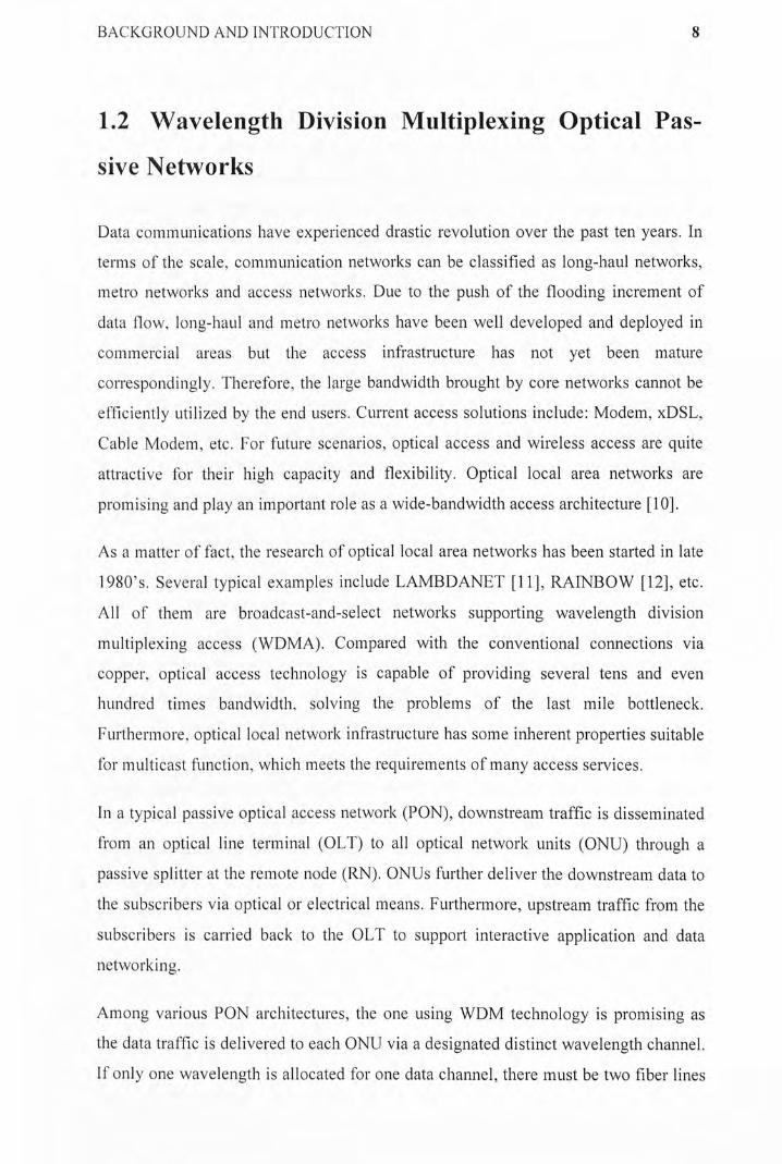
2.2 PON Architecture Using Downstream Optical
FSK Signals
In a typical W D M - P O N , traffics from the O L T are routed by one or more array
waveguide gratings (AWGs) at the remote node (RN) to different ONUs. The CLS
PON architecture using downstream FSK signals is shown in Fig. 2.1. Each
transceiver in the O L T is composed of a downstream FSK transmitter and an upstream
O O K receiver. The two wavelengths used in each FSK signal should be chosen to be
within the same passband of the A W G at the RN, where the downstream FSK signal is
routed to a respective O N U . At the O N U , the received downstream signal is split into
two parts, in which one is fed into the FSK receiver for downstream data detection and
the other for upstream data re-modulation. The FSK receiver consists of a narrowband
optical bandpass filter (OBPF) followed by a photodetector. Such receiver is much
easier to implement compared with that of DPSK signals [3], which requires either
coherent detection or optical interferometric demodulation before direct detection.
Moreover, phase information is more sensitive to environmental changes, which
makes the D P S K receiver unstable. The other part of received downstream signal
power is re-modulated with the upstream O O K data via an optical intensity modulator
at the O N U , and is then transmitted back to OLT. The two carrier frequencies of the
FSK signal, due to different group velocities in the fiber link, may experience walk-
off and the total intensity may not be kept constant after traveling for some distances.
DATA Rli-MODULATION ON D0WNSTR1:‘:AM OPTICAL FSK SIGNALS IN WDM-PONS 14
This may induce crosstalk to the re-modulated upstream signal. In order to maintain
the synchronization between the two complementarily modulated wavelengths in the
downstream FSK signal and to maintain the constant intensity property of the received
light at the O N U , proper dispersion compensation has to be carried out. This can
improve the transmission performance of the re-modulated upstream O O K data.
TX/RX1 卜 — — D o w ^ a m 力 : | 如 - , 。 卯 1 ———~~h 人,、\ (!^ / ONU 2
Tx/Rx 2 ^ ( ( ^ (
: AWG -g ^ AWG ' TT A,"""
Tx/Rx A/ : * Y ^ 「 • - ( ^ FSKT「丨—^ . / M \ L f S : R。
/ Upstream 厂 , i 、、.丨 ,
_ OOKRx k—- 、_ I O O K, J I RE-MOD
OLT RN Fig. 2.1 The CLS PON architecture using downstream FSK signals
2.3 CLS PON Demonstration Using Three Different
Optical FSK Transmitters
In this section, we have demonstrated the data re-modulation scheme for upstream
transmission in a CLS W D M - P O N using three different types of of optical FSK
transmitters at the OLT.
2.3.1 With an optical FSK transmitter based on direct modulation in
a DFB laser
The first demonstration uses the optical FSK transmitter based on direct modulation in
a DFB laser, which has been described in Section 1.1.2. W e have experimentally
demonstrated the proposed scheme on one particular channel in a W D M - P O N , for
simplicity. Fig. 2.2 shows the experimental setup. The DFB laser diode was directly

DATA IUi-M0I)ULAT10N ON D0WNSTI113AM OPTICAL FSK SIGNALS IN WDM-PONS 15
modulated by a 2.5-Gb/s non-return to zero (NRZ) pseudo random binary
sequence (PRBS). The driving D C and A C currents of the laser were 55 m A and 9
m A , respectively, resulting in an output signal with a central wavelength of 1545.76
nm and a frequency spacing of about 5 GHz. Driven by the complementary data signal,
an optical intensity modulator was placed after the DFB laser diode to compensate the
concurrent intensity modulation. By properly setting the driving signal amplitude and
the tunable electrical delay, the resultant output became an optical FSK signal with
constant intensity as shown in the inset eye-diagram of Fig. 2.2. The signal was then
amplified by an erbium-doped fiber amplifier (EDFA) to about 5 dBm and was
filtered by an optical bandpass filter (OF 1) with a 3-dB bandwidth of 0.8 nm. This
optical filler was used to emulate a channel of a 100-GHz A W G and also to suppress
the excessive amplified spontaneous emission (ASE). From the inset eye-diagram of
Fig. 2.2, the FSK signal was still kept constant-intensity after transmission over a span
of 20-km dispersion shifted fiber (DSF), operated in non-zero dispersion region.
Similar or better performance could be achieved with standard single mode fiber
(SMF) with lull dispersion compensation.
‘ 2.5Gb/s 1 1 i r x y l r ^ , : ~ I NRZ PRBS I H ^ r n Detector
FSK t ransmi t ter … , U _ : - 。 : “ i — 2.5Gb/s � — I ;; 丨 ‘ 1 —— NRZ
I ^ I :......•.......^^权[MimI 嶋 I V V JJ O O K t ransmit ter
Detector — IM: optical intensity mnrlijlafnri orwm ncjp PC: polarization controller zuKm uor
OLT ONU
Fig. 2.2 Experimental setup (Insets: eye-diagrams of the downstream FSK
signal at different locations, time scale: lOOps/div) DSF: dispersion shifted
fiber, EDFA: erbium-doped fiber amplifier, OF: optical filter.
At the O N U , the received downstream power was split by a 40:60 fiber coupler, of
which one output branch was connected to an optical frequency discriminator (0F2)
and a PIN detector. W e used a delayed interferometer with a relative delay of 94.3 ps
(corresponding free spectral range 〜2x5 GHz) as the frequency discriminator. As

DATA Rli-MODULATION ON D0WNSTR1:‘:AM OPTICAL FSK SIGNALS IN WDM-PONS 16
shown in the inset eye-diagram of Fig. 2.3, the 0F2 largely suppressed one of the
optical carriers and converted the FSK signal into a 2.5-Gb/s intensity modulated
signal, which was detected by a PIN photo-detector with a receiver sensitivity of -20
dBm, indicating negligible power penalty compared with the back-to-back case. The
other part of the received downstream signal power was fed into an optical intensity
modulator, driven by a 2.5-Gb/s N R Z 2"-1 PRES. The re-modulated upstream O O K
signal was then coupled into the upstream fiber link. The received upstream data was
detected by an A P D receiver at the OLT. Figs. 2.3 and 2.4 show the measured bit error
rate (BER) of the downstream and the upstream signals, respectively. Due to the
relatively small dispersion at the wavelengths around 1546 nm in the DSF, the two
optical frequencies experienced little walk-off and the upstream data suffered from a
very small power penalty of 0.2-dB, compared with the case of using C W laser as the
upstream data carrier.
1e-3 1 ;=ZZZ=:Z=I==ZIZ7 2 眷 Back-to-back
- o 20-km transmission 0
1e-5 -O
1 e - 6 -O
cr • 山 1e-7 -
QQ ;——•I r'l O 1e-8 - _ I _ _ _ , — , —
‘ ‘ i i i
1e-9 - O
• ; ' O
1 e-114 1 1 1 -i I 1 1
-23.0 -22.5 -22.0 -21.5 -21.0 -20.5 -20.0 -19.5 -19.0
Downstream average received power (dBm)
Fig. 2.3 B E R measurements for the downstream FSK signal in the back-
to-back case (•), and measured at the O N U after 20-km transmission (o). (Inset: eye-diagram of the demodulated FSK signal at the O N U , time scale:
lOOps/div)
DATA Rli-MODULATION ON D0WNSTR1:‘:AM OPTICAL FSK SIGNALS IN WDM-PONS 17
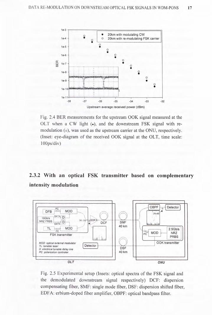
1e-3 -] -n
0 • 20km with modulating C W ie-4 - • Q o 20km with re-modulating FSK carrier
•
o 1e-5 - 拳
O 1e-6 - O
•
Q: ° IXJ 1e-7 - •
C Q ^ 丁 — — _ _ _ . . . . . 1 O
1e-8 - 一 一 _ 」 — 一 二— O
二 a i i ^ ^ U l ^ • • e i j • .
1 ‘ • J _ _ ‘ — — • — — — 一
1 e-11H n — ~ T " " " " — — ^ 1 1 -38 -37 -36 -35 -34 -33 -32
Upstream average received power (dBm)
Fig. 2.4 BER measurements for the upstream O O K signal measured at the
O L T when a C W light (•), and the downstream FSK signal with re-
modulation (o), was used as the upstream carrier at the O N U , respectively. (Inset: eye-diagram of the received O O K signal at the OLT, time scale:
lOOps/div)
2.3.2 With an optical FSK transmitter based on complementary
intensity modulation
3 p p ^ OBPF Detector]
r O F B 鬥 M O D ] 、 •—、 ,、 ,, i V* I i . J, 1 f,—、A /.—xX 29dB
� T 0 G b / s — l _ � £ ) l . � \ L { J i J . . MR7 pRRc I 丨:1;.丨 5(1:5(1 - EDFA- -^-^-— <
LNRZ_PRBS Dl…. / ? , . DCF SMF 、 , , , ,„„ ^ 40 km
[TL—.. - f ——[li^
PSK transmitter P》•工:―」 N R Z
, I — rKbo LiiJ__LLoJ /;•'•-.、 U
MOD optical external modulator ); O O K transmitter
TL: tunable laser Detector —
D: electrical tunable delay line DSF PC: polarization controller 4 0 k m
OLT ONU
Fig. 2.5 Experimental setup (Insets: optical spectra of the FSK signal and
the demodulated downstream signal respectively) DCF: dispersion
compensating fiber, SMF: single mode fiber, DSF: dispersion shifted fiber,
EDFA: erbium-doped fiber amplifier, OBPF: optical bandpass filter.
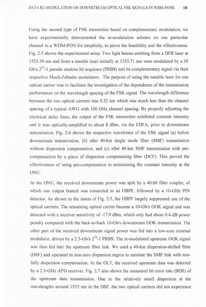
DATA Rli-MODULATION ON D0WNSTR1:‘:AM OPTICAL FSK SIGNALS IN WDM-PONS 18
Using the second type of FSK transmitter based on complementary modulation, we
have experimentally demonstrated the re-modulation scheme on one particular
channel in a W D M - P O N for simplicity, to prove the feasibility and the effectiveness.
Fig. 2.5 shows the experimental setup. Two light beams emitting from a D F B laser at
1553.39 nm and from a tunable laser initially at 1553.71 nm were modulated by a 10
Gb/s 2 -1 pseudo random bit sequence (PRBS) and its complementary signal via their
respective Mach-Zehnder modulators. The purpose of using the tunable laser for one
optical carrier was to facilitate the investigation of the dependence of the transmission
performance on the wavelength spacing of the FSK signal. The wavelength difference
between the two optical carriers was 0.32 nm which was much less than the channel
spacing of a typical A W G with 100 G H z channel spacing. By properly adjusting the
electrical delay lines, the output of the FSK transmitter exhibited constant intensity
and il was optically-amplified to about 8 dBm, via the EDFA, prior to downstream
transmission. Fig. 2.6 shows the respective waveforms of the FSK signal (a) before
downstream transmission, (b) after 40-km single mode fiber (SMF) transmission
without dispersion compensation, and (c) after 40-km S M F transmission with pre-
compensation by a piece of dispersion compensating fiber (DCF). This proved the
effectiveness of using pre-compensation in maintaining the constant intensity at the
O N U .
At the O N U , the received downstream power was split by a 40:60 fiber coupler, of
which one output branch was connected to an OBPF, followed by a 10-GHz PIN
detector. As shown in the insets of Fig. 2.5,the OBPF largely suppressed one of the
optical carriers. The remaining optical carrier became a 10-Gb/s O O K signal and was
detected with a receiver sensitivity of-17.9 dBm, which only had about 0.4-dB power
penalty compared with the back-to-back 10-Gb/s downstream O O K transmission. The
other pari of the received downstream signal power was fed into a low-cost external
modulator, driven by a 2.5-Gb/s PRBS. The re-modulated upstream O O K signal
was then fed into the upstream fiber link. W e used a 40-km dispersion-shifted fiber
(DSF) and operated in non-zero dispersion region to emulate the S M F link with non-
fully dispersion compensation. At the OLT, the received upstream data was detected
by a 2.5-GHz A P D receiver. Fig. 2.7 also shows the measured bit error rate (BER) of
the upstream data transmission. Due to the relatively small dispersion at the
wavelengths around 1553 nm in the DSF, the two optical carriers did not experience

DATA Rl i-MODULATION ON D0WNSTR1:‘:AM OPTICAL FSK SIGNALS IN WDM-PONS 19
too much walk-off and the upstream data only suffered from a very small power
penalty (〜1-dB), compared with the case of using C W laser as the optical carrier. It
could be expected that if S M F had been employed as the upstream fiber link, the
upstream signal quality could have been kept good provided that proper dispersion
compensation was carried out.
! !
_ [ —
! I I : ^ ^
Fig. 2,6 Waveforms of downstream signals: (a) the output of FSK
generator, (b) the FSK signal after 40-km S M F transmission without
dispersion compensation, (c) the FSK signal after 40-km S M F with DCF
pre-compensation. indicates zero level)
1e-4 - • •
• 2.5 Gb/s T
ie-5 - � r e m o d u l a t e d • o upstream •
① ie-6 - o • O O K d a t a •
fg • (APD receiver)
§ 1e-7 - O 參 •
t O T
^ 10Gb/s
m • downstream •
° • O F S K data • ie-9 - ,, ‘ . , o • (PIN receiver) •
Upstream data ^ ^ modulated with •
- C W injection 〇 •
1e-11 ~I 1 1 1 1 1 1 1
-32 -30 -28 -26 -24 -22 -20 -18
Average received power (dBm)
Fig. 2.7 B E R measurements of downstream FSK data (•), upstream O O K
data re-modulated with downstream light (•) and upstream O O K data
modulated with C W carrier (〇)’ after respective 40-km transmission.
To further characterize the FSK signal transmission, the wavelength spacing of the
two optical carriers per FSK signal was varied and the signal quality of both the

DATA Rli-MODULATION ON D0WNSTR1:‘:AM OPTICAL FSK SIGNALS IN WDM-PONS 20
downstream and the upstream signals was examined. Such wavelength spacing {AX)
had an upper bound (nominally, A A. < 0.35 nm), which should correspond to the
passband of the common A W G s (100-GHz spaced) or similar types of wavelength
demultiplexers. On the other hand, if AX was too small, a very narrowband OBPF
might be needed. In addition, due to the non-zero rise/fall time and the non-ideal
signal extinction ratio, the data spectra of the two optical carriers overlapped and
interfered with each other. This greatly deteriorated the signal quality of each optical
carrier, especially when A A, was very small and the bit rate was high. Fig. 2.8 shows
the measured B E R curves as well as the power penalty curve (at BER=10“))of the
downstream FSK signal when AX varies. When AA. was less than 0.24 nm, poor
transmission performance in the 10-Gb/s downstream signal was resulted, mainly due
to the spectral overlapping between the two optical carriers. Such spectral overlapping
also led to intensity fluctuation at the O N U and thus degraded the upstream signal
quality.
1e-2 -1 r
1e-3 - © • \ - 6 A \ # \ • — Downstream BER 尝
1e-4 - Gk. © — Upstream BER ^ \ A Downstream penalty ro
1e-5 - \ H (at BER=1e-9) - 4 § ^ ^ ?
LU ^ 5
^ 1e-7 - K • 2 ^
1e-8- 姿
1e-9 - ——A-^ • - 0 I
^^ o
16-10 € ] > © — © c Q
1e-11 — I — 1 1 1 1 1 1 1- -2
0.00 0.05 0.10 0.15 0.20 0.25 0.30 0.35 0.40
W a v e l e n g t h d i f f e r e n c e A A. ( n m )
Fig. 2.8 B E R of downstream/upstream transmission and power penalty
curve of the downstream FSK signal versus the wavelength spacing
between the two optical carriers of the downstream FSK signal. Left y-
axis is B E R of downstream/upstream transmission and the right one is the
downstream signal power penalty at BER=10''\

DATA Rli-MODULATION ON D0WNSTR1:‘:AM OPTICAL FSK SIGNALS IN WDM-PONS 21
2.3.3 With our proposed optical FSK transmitter based on phase
modulation
2.3.3.1 The proposed optical FSK transmitter
i 个 L 个人I Frequency | i response of DM i ! V 、 、 、 I 、 ’ ’ \ I
Pre-coded data i '' ‘ ~ ‘ ‘ ~ ~ W a v e l e n g t h i at Bjops -;;:- ‘‘
PM I——i£iil_ … _ ~
? … L L - J LU... A.:
(a)
i oL'f"" 丨 厂 Rf l I I r. 二 i I " " “ I
J — — ^ — — ^ ― ^ > r^i i ; J > 1 a
I 口s /A- lixN . g ~~^! 二 T 乏 1 • ONUW I
阁 . “ � �I U M i EI iSs � ‘ • r — , j ^ i i ^ i < S 2 I二 TO< Rx — ~ 》 • I ! V i: 05
I^O I 丨 1 � ~ !3 “ “ j “ “ 〕
(b)
Fig. 2.9 (a) Proposed FSK transmitter using phase modulator (PM); (b)
CLS P O N architecture
Fig. 2.9 illustrates the operation principle of the proposed optical FSK transmitter [22].
Two C W light beams with small wavelength spacing are combined and fed into a
LiNbO} phase modulator where both of them are phase modulated with the
differentially pre-coded data signal at B bps. The output then passes through a delay
interferometer (DI) with a relative propagation delay of AZ. The wavelengths of the
two optical carriers are chosen in such a way that they satisfy the conditions
"丨 n , A L 门 1 �
/I, = - ^ ’ a n c U 〗 = " " “ ( 2 . 1 ) m, w, 4-1/2
DATA IUi-M0I)ULAT10N ON D0WNSTI113AM OPTICAL FSK SIGNALS IN WDM-PONS 22
where AL is the propagation distance of one data bit in the DI; n\ and ni are the
respective refractive indices experienced by X\ and /I2 in the DI; and m\ and mi are
positive integers. This means that the wavelengths of the two optical carriers are
chosen in such a way thai one wavelength (山)coincides with the minimum
transmission point of the DI whereas the other wavelength (/I2) coincides with the
maximum transmission point (as shown in Fig. 2.9). Thus the DI essentially converts
the phase-modulated optical signals into intensity-modulated ones. In addition, the
output produced by these two wavelengths would be complementary to each other. As
a result, the combined output exhibits constant optical intensity as illustrated in Fig.
2.9 (a).
The CLS W D M - P O N architecture using the proposed downstream FSK transmitters is
shown in Fig. 2.9 (b). Each transceiver in the O L T is composed of an upstream O O K
receiver and the proposed downstream FSK transmitter, which includes a pair of C W
sources and an optical phase modulator driven by the respective differentially pre-
coded downstream data. In addition to satisfying the condition stated previously, the
spacing of each wavelength pair is also chosen to fit into the passband of one array-
waveguide grating ( A W G ) channel. The multiplexed signal from all the transmitters is
then fed into a common DI to generate the downstream FSK signal to be transmitted
to the O N U . With proper dispersion compensation, the constant intensity of the
downstream FSK signal can be preserved at the O N U side. In the O N U , part of the
received power is tapped out for downstream data demodulation and reception
through optical filtering. The rest of the downstream power is then intensity
modulated with the upstream data and sent back to the O L T via the transmission link
and the A W G .
2.3.3.2 Experimental demonstration
Fig. 2.10 shows the experimental setup to demonstrate our proposed scheme. The
outputs from the two D F B lasers (LDl & LD2) were combined with a 50/50 fiber
coupler. The combined signal was then phase-modulated by a 9.953-Gb/s N R Z
pseudo random binary sequence (PRBS) via the optical phase modulator (PM). The
DATA Rli-MODULATION ON D0WNSTR1:‘:AM OPTICAL FSK SIGNALS IN WDM-PONS 23
signal was then amplified by an E D FA to about 5 d B m and filtered by an optical
bandpass filter (OBPFl) with 3-dB bandwidth of 0.8 nm. This optical filter was used
to emulate a channel of a 100-GHz A W G and also to suppress the excessive amplified
spontaneous emission (ASE). A fiber-based DI with a relative delay of 94.3 ps was
placed after the optical filter to generate the desired downstream FSK signal, as shown
in the inset of Fig. 2.10. The wavelength of LDl (1552.95 nm) was exactly aligned at
the maximum transmittance point of the DI while that of LD2 (0.65 nm apart from
LDl) was aligned at the minimum transmittance point. From the inset waveform of
Fig. 2.10, the FSK signal experienced nearly no walk-off and still kept constant-
intensity alter transmission over a span of 20-km dispersion shifted fiber (DSF),
operated in non-zero dispersion region. Similar or better performance could be
achieved with standard single mode fiber (SMF) with full dispersion compensation.
OLT ONU
FSKTransmitter
r 0BPF2 i 10-Gb/s I i ^ n . 10-Gb/s i m PG 1 丄 — E D •I D1 • ! DI i 20-km \ (/V 丨 LD1 5 、 i p. 0 ^ 1 I DSF ) . 一 , 一‘ I i m H PM U 0 ~ ~ ^ ^ — — 瞧 I,丨,丨丨 iLD2ty 1 IX I ( \ ! I X T EDFA j 「 / m
-L, -, - r ^ [J 2.错/s
^ ^ ^ Fig. 2.10 Experimental Setup. PG: pattern generator, PM: phase modulator,
EDFA: erbium-doped fiber amplifier, OBPF: optical bandpass filter, DI:
optical delay interferometer, DSF: dispersion shifted fiber, ED: error
detector, ATT: optical attenuator.
At the O N U side, the received downstream signal was split by a 40/60 fiber coupler.
One branch of the output was filtered by an optical grating filter (0BPF2) with a 3-dB
bandwidth of 0.2 nm and was then detected by a 10-Gb/s PIN receiver. As shown in
the upper inset of Fig. 2.12, the filter suppressed one of the wavelengths by about 40
dB, effectively converting the wavelength modulation into intensity modulation as
could be observed from the eye-diagram shown in Fig. 2.12. The B E R curves shown
in Fig. 2.12 reveal a power penalty of only 0.1 dB when compared with the back-to-
back case. The other part of downstream optical power was fed into an optical
DATA Rli-MODULATION ON D0WNSTR1:‘:AM OPTICAL FSK SIGNALS IN WDM-PONS 24
intensity modulator, driven by a 2.488-Gb/s N R Z PRBS upstream data. The re-
modulated upstream O O K signal was then coupled into another span of 20-km DSF.
The received upstream data at C O was detected by a 2.5-Gb/s A P D receiver. The BER
curve shown in Fig. 2.13 indicates a sensitivity of -33.2 dBm and a power penalty of
less than 0.1 dB when compared with the back-to-back case. These results
demonstrate the effectiveness of this FSK transmitter and the re-modulation scheme in
W D M - P O N .
I'SENSI -?0|dBm -E.35 dB l】0.0 I dB/[ lU ^ MRRK :R
圓 • 画
CENltft 1553.29 nm~ SPAN 10.00 nm »RB 0.0B nm UB B kHz ST=>75 msec
Fig. 2.11 Optical spectra of the downstream FSK signal; Inset: waveforms
of two wavelength components (50ps/div)
-3 r 1 1 1 1 "I ‘ I", ••‘ I ' ' ' -• Back-to-Back
A A 20-km Transmission
auMULi j
-4 • • A = ^ :-—_. - —_,、、, ~ —
• V ;
^ -5 • A " ^ — “ 1 -
m _ wavelength 2 ^ A O) -D O
• •7 - -
I 20 ps/div : I L
- [ M M j • ^ - 1 0 - ‘ A -
I A
'-22.5 — ~ - 2 V " 2 I -20.5 ^ ― -19.5 -19 -18.5
Received Optical Power (dBm)
Fig. 2.12 BER, eye-diagram and optical spectrum of 10-Gb/s downstream
FSK signal

DATA Rli-MODULATION ON D0WNSTR1:‘:AM OPTICAL FSK SIGNALS IN WDM-PONS 25
-4 I 1 1 I I ——1
• Back-to-Back
^ A 20-km Transmission
A -5 • “
A •
I -6 - % i 丨 A O I • —I
-7 丨 S
; 1 1 0 0 ps/div : L
、/ ••; g A : A
幽
"^-37 — -36 -35 -34 -33 -3:
Received Optical Power (dBm)
Fig. 2.13 B E R and eye-diagram of 2.5-Gb/s upstream re-modulated O O K signal
To further investigate the performance of FSK signal transmission, we varied the
wavelength spacing of the two carriers and measured the power penalty for both the
upstream and downstream data with respect to the case of 0.65-nm wavelength
spacing. The wavelength spacing was discretely tuned from 〜0.16 nm to 0.98 nm by
adjusting the temperature controllers of the two DFB lasers. Note that with a fixed DI,
there are only a finite number of wavelength pairs within OBPFl passband that satisfy
the FSK condition given in the previous section. Fig. 2.14 shows the measured results.
For the wavelength spacing ranging between 0.32 nm and 0.65 nm, negligible power
penalty was achieved. However, when the wavelength spacing was tuned to be less
than 0.23 nm, severe interference between the two wavelengths was observed. It
resulted in large amplitude fluctuations in the downstream FSK signal. This inevitably
deteriorated the downstream signal quality, which in turn, adversely affected the re-
modulated upstream O O K signal. Besides, such narrow wavelength spacing also
hindered the demodulation of downstream signal with optical filtering. On the other
hand, when the wavelength spacing was set beyond 0.65 nm, both the upstream and
the downstream signals were increasing degraded. This could be attributed to the
increased amplitude fluctuation in the FSK signal due to larger walk-off between the
two wavelengths and the signal distortion caused by band-edge filtering at OBPFl.
Moreover, excessive wavelength spacing would increase the signal leakage into the

DATA IUi-M0I)ULAT10N ON D0WNSTI113AM OPTICAL FSK SIGNALS IN WDM-PONS 26
adjacent channels and induced channel crosstalk. Thus, the optimal wavelength
spacing for the FSK signal was found to be within the range from 0.23 nm to 0.65 nm.
6 1 I
• lO-GWs Upstream
g 0 O 2.5-Gb's Dcwistream
_ 4-CQ
S 3-ro
5 R e f e r e n c e Po in t CL S3 I
1- * o J
0- 拳 0 Q J g ( i眷 春 春 參
-1 1 1 1 1 1—'
0.2 0.4 0.6 0.8 1.0
V\fevelength spacing (nm)
Fig. 2.14 Power penalty at BER=10'^^ for different wavelength spacing of
downstream FSK signal.
2.4 System Performance by Using Phase Modulation
Based FSK Transmitter
In our proposed optical FSK transmitter based on optical phase modulation, the
generated FSK signal quality greatly depends on the selected wavelengths and the
relative arm delay of the optical delay interferometer [22]. This can be explicated
through Eq. (2.2). The output optical power from one port of the DI has a relation with
the differentially precoded input bits (p„ and the optical frequency co, as well as
the relative delay T, Therefore, for a specific precoded bit, the output power is
uncertain unless [coT) is fixed. Thus, the term {coT) should be properly selected
according lo Eq. (2.1) to guarantee a best-quality FSK signal generated. However, in
practical systems, co may be shifted because of the output frequency drift of laser
sources and T may also shift due to the variation of the temperature of the DI. In this
section, these inHuences on system performance are investigated. Besides, fiber
DATA IUi-M0I)ULAT10N ON D0WNSTI113AM OPTICAL FSK SIGNALS IN WDM-PONS 27
dispersion is also counted in the study as it would also greatly affect the quality of the
optical FSK signal.
1 1 2
“ 2 2
=丄尸+丄+丄/>. + 丨)+."…厂 4 4 2
P (2.2) 一 (l + cos(yr),for precoded bit 1 ;
二 < p
—(1 - cos coT), for precoded bit 0
2.4.1 Wavelength detuning of light sources
A few factors may cause wavelength drift in light sources. Both the operating
temperature and the pumping current may shift the output wavelength of a laser diode.
The temperature induced passband shift of a filter for wideband spectra slicing
purpose would also change the light source's wavelength. As stated in the last
paragraph, since the phase modulation based FSK transmitter has stringent constraints
on wavelength detuning of light sources, the influence to the system performance will
be discussed in this section.
The ideal output power of a specific optical FSK bit from our proposed transmitter can
be determined according to Eq. (2.2), and will affect the detection and decision at the
FSK receiver unit. Thus the system degradation due to wavelength drifting of the light
sources can be estimated by varying co and determining the corresponding power as
well as BER based on a probability model. But such estimation does not take into
account quite a few of practical considerations, so we have carried out the following
experimental investigation. The experimental setup is shown in Fig. 2.10. W e varied
the wavelengths of the two DFB lasers in the FSK transmitter structure, according to
the modes listed below, and obtained the measurements of induced power penalty at
the receivers, as depicted in Fig. 2.15. The other components in the system were
maintained at their normal states of operation as the same as the demonstration in
Section 2.3.3.
DATA Rli-MODULATION ON D0WNSTR1:‘:AM OPTICAL FSK SIGNALS IN WDM-PONS 28
The downstream optical FSK signal performance was firstly measured. Since the
downstream signal quality was mainly determined by the optical carrier that was
extracted by the OBPF2 for downstream detection, we detuned only this wavelength
(in this experiment it was the short wavelength of the FSK signal) and kept the other
one unchanged. The round circles in Fig 2.15 depict the corresponding downstream
penalty: the downstream FSK signal quality was very sensitive to the short
wavelength detuning - even a detuning of 0.01 nm led to a power penalty (at
BER=10“))as much as 3 dB. This could either be foreboded by Eq. (2.2) or be
understood by means of the DI,s frequency response shown in Fig. 2.9. The frequency
response of the DI is periodic with a cycle of 10 GHz, corresponding to about 0.08 nm,
therefore even 0.01-nm shift with respect to the maximum transmittance point can
induce a large change in the transmittance, which successively causes the signal
degradation in the demodulated FSK signal. Detuning towards either direction
(towards shorter or longer wavelength) would cause similar penalty but they were not
totally symmetric, which might be attributed to the birefringence of the DI that was
not considered in the ideal theoretical formula in Eq. (2.2).
• Downstream penalty (tuning short X only) • Upstream penalty (tuning short 入 only)
• Upstream penalty (tuning both: short A, decreases, long A, increases)
• Upstream penalty (tuning both: short X decreases, long X decreases)
8 - •
S 6 -
f • • 艺 4 - • • •
I • h - • • • • • • •
• • • • • •
0 - • • a • 化 眷 • • • I 1 1 1 1 1
-0.03 -0.02 -0.01 0,00 0.01 0,02 0.03
Short wavelength's detuning (nm)
Fig. 2.15 The measured power penalty of both downstream and upstream
signals when altering the wavelengths of the FSK signal according to the
stated modes

DATA IU-:-M()DULATK)N ON DOWNSTREAM OPTICAL FSK SIGNALS IN WDM-PONS 29
The upstream O O K signal performance will also be influenced with respect to the
wavelength detuning of both of the wavelength carriers in the optical FSK signal. In
our investigation, we firstly fixed the long wavelength and detuned the short one,
finding out that the upstream data quality behaved like the dotted curve. For the same
wavelength detuning as the previous downstream case, the power penalty of the
upstream signal was much less than that of the downstream signal. As only the short
wavelength was drifted and the other one was preserved, the total fluctuations of the
combined FSK envelope were not so drastic. Moreover, since the upstream data was
at 2.5-Gb/s and a lot of fast fluctuations could be filtered out at the receiver side in the
OLT. W e have also inspected the case when both of the wavelengths were drifted. The
triangular symbols in Fig. 2.15 stand for the case when the short wavelength was
decreased and the long wavelength was increased, while the squares depict the case
when both of them decreased. Il shows that the signal deterioration tended to be a little
smaller than the case when only the short wavelength was detuned, as the combined
temporal fluctuation of the two wavelengths was even a bit smaller than the former
case. This could be explained from the DI response shown in Fig. 2.9. When the short
wavelength deviated from the maximum transmittance point of the DI, the
transmittance of the long wavelength ascends, so the resultant fluctuation is muted.
2.4.2 Detuning of the DI frequency response
10 -]
• Downstream (10-Gb/s FSK) 8 - o Upstream (2.5-Gb/s O O K ) •
m 6 - •
^ • ro S 4 - •
I • • o 2 - 拳
Q . •
眷 • 0 - o O o o * o O o o o
I I \ ‘ I I
27.9 28.0 28.1 28.2 28.3 28.4
Temperature of DI ( � C )
Fig. 2.16 The power penalty versus the temperature of the DI in the FSK transmitter

DATA Rli-MODULATION ON D0WNSTR1:‘:AM OPTICAL FSK SIGNALS IN WDM-PONS 30
In the process of FSK generation, the DI demodulates the two phase modulated optical
frequency carriers into complementary intensity modulation. The temperature
variations induce changes in the effective relative delay {T in Eq. (2.2)) of the Dl and
this will bring similar impact on the system performance. For the downstream signal,
the relative delay drifts bring severe performance degradation, and its mechanism is
similar to that of short wavelength detuning as explained in Section 2.4.1. From Eq.
(2.2), the output power P at the best case evolves to (P/2) • (1 + cos coT). In frequency
domain, variation of T shifts the frequency response to the lower or higher frequencies.
A little shift of the frequency response can cause a drastic change of the output power
and the signal quality. On the other hand, however, the detuning of the temperature of
the DI caused nearly no power penalty to the upstream receiver performance at the
OLT. The reason behind this phenomenon is that, though both the optical carriers'
intensity-modulated signals have been degraded due to the DI's frequency response
shift, and the combined optical power of the two wavelengths,
{P /2)(1 + cos coT) + 12)(1 - cos coT) = P analytically, is kept almost unaltered.
2.4.3 Dispersion tolerance
. 眷 with 40-km roundtrip DSF
拳 o o with 13.2-km roundtrip S M F
參 1e-5 - O
lU , , 眷 CD 1e-6 - • o
i • O ^ 1e-7 - 參 00
Q . • O ID
1e-8 -• o
1e-9 -
• O
1e-10 -l 1 1 1 1 1 1
-37 -36 -35 -34 -33 -32 -31 -30
Average received power (dBm)
Fig. 2.17 The B E R curves for different transmission media in the CLS P O N

DATA IUi-M0I)ULAT10N ON D0WNSTI113AM OPTICAL FSK SIGNALS IN WDM-PONS 31
In the system demonstration in Section 2.3.3, a piece of 20-km DSF was used to
emulate the S M F with proper dispersion compensation. The residual dispersion was
estimated to be 0.5x40x0.65=13 (ps) provided that the dispersion parameter at around
1553 nm is 0.5 ps/nm/km. In this investigation we used a piece of 6.6 km S M F to
emulate the case with a large residual dispersion (estimated as 16x6.6x0.65=137.3
(ps)), so as to study the dispersion tolerance of the generated optical FSK. W e have
found that there was nearly no impact to the downstream receiver sensitivity.
However, the upstream signal was evidently degraded as it was re-modulated on the
downstream optical FSK carrier, which had experienced some dispersion and walk-off.
As shown in Fig. 2.18(a), the eye was totally closed at the direct-detection receiver in
the OLT. However, by adding a 1.97-GHz electrical bandpass filter, the eye opened
and the signal could be detected with a power penalty of 2-dB compared with the
previous demonstration, as most of the noise (Fig. 2.18(c)) in the high frequency
regime had been removed by the filter.
1 j T i prrrnmBnonr~n———fTrrnori i i t g ca d B / P u j T nuc 'UR -'8.7 iffi!n
• f + : • ; 國 翌5二“2亟三三三:=
卞’ 、 ‘V ” , I 1
; I i { L I I I I I I I j 1 I ^TMl I W m §ICirid.50 Clii • - I‘.‘_,. — . . .1 — i... -i- —— —••• RB 3.tlB tlKz yS 308 kHz ST 147.? isec
(a) (c) ! ! 1 1 1 i 1 1 ifliiEU D d3~rarmi~—~jisi.B; dB
; i j i i j i i i.Si d B / 0 IJ ! 1 i j I I I j iTT-' — I—.."'i i — : i : 「 h ‘ ! ‘ 1 ! -明、L|-'
: 三 》 竺 ! ••«• % J —Passbaiiti~trf-t ie
: 主 竺 i I i • t ! i • ! k } m \ l i r W s i o p I 0 . 5 B m j * 丄 • i ‘ 丄…… • - -••••-• ’. R6 3.00 tWt ue 300 VHi ST 147.8 n&ec
(b) (d)
Fig. 2.18 The eye diagrams of the received upstream O O K signal: (a)
without electrical filter (200 ps/div), (b) with a 1.97GHz bandpass filter
(200 ps/div); and the electrical spectra of the detected upstream light: (c)
the FSK carrier without re-modulated data, (d) the FSK carrier with
upstream O O K data. The broken line simulates the shape of the electrical
filter.
DATA Rli-MODULATION ON D0WNSTR1:‘:AM OPTICAL FSK SIGNALS IN WDM-PONS 32
2.5 Summary
Table 2.1:
Direct modulation Complementary Phase modulation
based modulation based based
Speed Medium (1:2.5 Gb/s)High (—10 Gb/s) High “10 Gb/s)
Complexity/Cost Lowest Medium Low
Signal quality High Medium Highest
From the three CLS P O N demonstrations using different optical FSK transmitters, we
have summarized and compared their relative pros and cons with respect to operation
speed, system complexity, and signal quality, as illustrated in Table 2.1. Generally, the
direclly-modulated laser based one can produce only j2.5-Gb/s FSK signals, due to
the limitation of its modulation bandwidth, while the other two can latently achieve
— 10-Gb/s operations. On the other hand, it is obvious that the complementary
modulation based transmitter is the most complex, incarnated not only in most
components incorporated but also in meticulous relative delays between the
complementary input data signals. All three approaches are capable to attain sound
signal performance shown in the BER measurements figures. Although the two
demonstrations using direct modulation based FSK transmitter and phase modulation
based one had similar downstream received power at BER=10"^, the latter one with
much higher operating speed (10 Gb/s) had better signal quality than the former one,
as the shot noise accompanied with the former signal in the receiver was larger. (The
details of this statement may refer to Chapter 4.)
The CLS P O N using our proposed phase modulation based FSK transmitter is capable
to achieve high-speed operation and good performance while relatively low cost. Its
system performance closely depends on the alignment of FSK carrier wavelengths to
the Iransmillance response of the DI. The system degradation has been studied, with
respect to both the FSK frequency detune and the DI's temperature drift. The
downstream signal potentially suffers from more severe degradations than the
DATA Rli-MODULATION ON D0WNSTR1:‘:AM OPTICAL FSK SIGNALS IN WDM-PONS 33
upstream signal. Therefore, it is suggested that the light sources as well as the DI
should be precisely stabilized for practical applications. In addition, experimental
investigations show that the requirement of dispersion compensation is not too
stringent and some residual dispersion does not degrade the system severely.
INTENSITY-MODULATED LABELLING ON OPTICAL FSK OR DPSK PAYLOADS IN OLS NETWORKS 34
3 Intensity-Modulated Labelling on
Optical FSK or DPSK Payloads in
OLS Networks
3.1 Existing Labelling Schemes and Their Features
A widely referred optical packet switched network architecture is so-called optical
label switching (OLS), which is the extension of the suggested generalized multi-
protocol labelling switching (GMPLS) [16]. OLS is an attractive approach to support
low-latency and efficient packet routing and forwarding for future high-speed optical
packet networks. In OLS networks, an optical label is encapsulated into every
incoming optical packet at the ingress router to provide routing information for the
next hop. Label swapping is performed at each core router to update the content of the
label. Fig. 3.1 shows the typical architecture of an OLS network. At the ingress edge
router, each incoming data packet in various formats is firstly processed, including
routing message collection, label generation, packet packaging, etc. The packet is
affiliated with an optical label and is forwarded to the next hop through the switch
fabric, along the established network path. At the first core router, part of received
optical power is tapped out for label extraction and processing. Up to now there are
few truly all-optical implementations in such processings. In [23], optical code (OC)
labels were employed and optically processed by optical correlators, before further
detection and controlling function in electronic domain. In [24], both the processing
and the switching were demonstrated all optically through a terahertz optical
asymmetric demultiplexer (TOAD), but only a limited amount of label patterns could

INTENSITY-MODULATED LABELLING ON OPTICAL FSK OR DPSK PAYLOADS IN OLS NETWORKS 35
be processed and complicated physical-layer structure were employed. Therefore, in
general, a common approach is to realize the function of label processing electrically
but to do label extraction and swapping all optically.
For the rest of optical power of the received optical packet, the old label should be
removed by a label erasing unit (LEU), before the new label is added into the packet
payload. In this way, all-optical label swapping is achieved. With the current
technology this technique can be implemented all optically and the realization and the
possible improvement keep attracting plenty of research interests. In the following, we
will briefly review several all-optical labelling schemes proposed in the recent years.
: J Packet J switch fabric I 1 I ~ ~ ^ M l Old label I J New label |I I switch fabric I ^ ‘ formation 一—一 H processing |T"in removal \ insertion |I" 一
;label generation ^ | demultiplexing I ii-c fe l a ^ s w ^ i ^ _ _ j packaging 丨 . i . , ,: ~ ~ - — —
'controlling 丨 : v + Label extraction , j I j ! and processing
E d g e rou ter � Co re router C o r e / e d g e router • . . ‘ . • f •
Network management unit
Fig. 3.1 The processing in an OLS network
3.1.1 Bit serial labelling
In this scheme, labels and payloads are distributed in different time slots in optical
packets. Fig. 3.2 shows the packet format of such labelling scheme. In general, both
payloads and labels are in optical O O K format, and most probably, labels have equal
or lower bit rate than payloads.
packet 1 packet 2 guard band
labeH payload 1 Iabel2 pay load2 . , .
Fig. 3.2 The bit serial labelling

INTENSITY-MODULATED LABELLING ON OPTICAL FSK OR DPSK PAYLOADS IN OLS NETWORKS 36
All optical label swapping can be implemented via an optical exclusive O R (XOR)
operation [25], in which a locally generated new optical pulse train is used to modify
the existing optical label through the X O R gate to generate the new optical label. In
this way, the optical label is renewed or updated. This labelling scheme together with
its all-optical label swapping function needs precise time synchronization between
new label bits and the optical packet consisting of both payload and label.
3.1.2 Subcarrier multiplexed (SCM) labelling
In this method, the label information is modulated onto a subcarrier frequency which
is then combined with the payload on the same optical carrier via subcarrier
multiplexing. Therefore, in time domain, the label and the payload information is
overlapped in a same time period. However, they are separable in the spectral domain
so that they are easily separated by means of narrowband optical filtering at the
receiver part of each node. Fig. 3.3 shows a typical spectrum of such a S C M labelled
signal.
Optical Opt ical carrier power
S C M A Payload label / \ l\ \ l\ S C M
/ \ label
~IJ I iJ \ ~ ~ U • … T . r opt ical f requency Subcarrier frequency 严 ^
Fig. 3.3 Optical S C M labelling
A simple and successful demonstration of S C M label extraction was done by optical
filtering using fiber Bragg grating (FBG) [26]. By using a FBG with designated centre
wavelength and bandwidth, the optical payload is reflected while the S C M label
would pass through it. Then the S C M label is processed and a new label is generated
before it is combined with the pure payload that is reflected by FBG. Thus the all-
oplical label swapping is attained.

INTENSITY-MODULATED LABELLING ON OPTICAL FSK OR DPSK PAYLOADS IN OLS NETWORKS 37
The label swapping of S C M labels is easier to implement to some extent than the bit
serial ones, since no stringent time-domain synchronization is needed. However, it
requires a wider channel spectrum so as to accommodate the S C M label carrier.
Moreover, both the label and the payload signals may be degraded due to the possible
crosstalk between the label and the payload for non-ideal optical filtering.
3.1.3 Orthogonally modulated labelling
Orthogonal modulation in optical communications constructs a special format in
which the optical carrier is both intensity modulated and angle modulated to carry two
different sets of data. For example, one set of data in A S K format while the other set
of data in DPSK or FSK format. Since both sets of data are superimposed in time and
frequency domains, the spectral and bandwidth efficiencies are higher than the
previous schemes. Besides, the two sets of data can be demultiplexed orthogonally
and be detected at the receiver side.
label I
""“processing | , J new D P S K
E 1 y label
丨"」1:10 CO—CM.|i! r ^ ^ _
n e w \ /
丨洲 z . . / y - r ~ K p
& / 人out / \ ] ^oui g j ~ j SOAs ) fj
tunable / ^ K Phase laser / modulator
n e w F S K single InP chip label
Fig. 3.4 Label swapping in an orthogonal labeled OLS network (After Ref. [27])
In previous implementations of such orthogonal labelling scheme, FSK or DPSK
format was used for the slow label data while A S K for the high-speed payload data
[27]. The A S K payload data was modulated on the optical carrier through an optical
intensity modulator, after the DPSK or FSK label data was generated via an optical
phase modulator or an optical FSK transmitter based on direct modulation in a DFB

INTENSITY-MODULATED LABELLING ON OPTICAL FSK OR DPSK PAYLOADS IN OLS NETWORKS 38
laser [28]. At the core routers, the angle-modulated label should be firstly
demodulated before the label processing. The erasure of the angle modulated label
was realized by means of wavelength conversion. Then the new optical label was
inserted to the optical payload again. The label swapping procedure is depicted in Fig.
3.4.
3.2 The Proposed OOK Labelling Scheme and OLS
System Architecture
In the orthogonal labellling scheme listed in the previous section, the low-speed label
was angle-modulated onto the intensity-modulated payload. The label was in optical
differential phase-shift keying (DPSK) or optical frequency-shift keying (FSK)
modulation format, which was orthogonal to the on-off keying (OOK) modulated
payload. Thus, at each core router, an optical delayed interferometer or a frequency
discriminator was required to demodulate the label for processing and then an optical
phase modulator or a new tunable light source was needed to generate the new optical
DPSK or FSK label. Moreover, the label swapping was realized by means of
wavelength conversion. In [29], optical DPSK signal was employed as the payload, on
which the O O K label was superimposed. The O O K label was erased by means of
optoelectronic complementary modulation [30]. Since optical FSK has attracted
much attention lately due to its possibly superior transmission performance compared
with O O K and DPSK [2], we propose and investigate another angle modulation
formal, optical FSK, for the high-speed payload, while the O O K label is superimposed
onto it. In addition, we propose a new method to implement the all-optical label
swapping of the intensity-modulated label. To further prove the feasibility and
effectiveness of the proposed all-optical label swapping scheme, we also investigate
the label swapping in the case of using DPSK payload. W e have experimentally
demonstrated 40-km transmission and all-optical label swapping of 1.244-Gb/s O O K
label on 9.953-Gb/s angle-modulated packet payload, for both optical FSK and optical
D P S K payload cases, with small induced power penalty.

INTENSITY-MODULATED LABELLING ON OPTICAL FSK OR DPSK PAYLOADS IN OLS NETWORKS 39
Fig. 3.5 shows the system architecture of the OLS network with the proposed labelling
scheme. At the ingress edge router, each incoming angle-modulated optical packet is
assigned a label generated by the network management unit. The generated label is
then used to externally modulate the constant intensity of the optical packet payload.
The composite packet is then forwarded to the next core router along the established
network path. Proper extinction ratio (ER) of the O O K label signal should be
maintained to guarantee the signal quality of the label to be equal to or a bit better
than that of the optical packet payload, to ensure reliable routing and forwarding can
be achieved. At the core router, part of received optical power is tapped out and is
detected directly, as the label is in O O K format. For the rest of the received optical
power, the label signal is removed by the label erasing unit (LEU). The label-erased
optical payload signal is then intensity modulated with the newly generated label. In
this way, all-optical label swapping is achieved and the optical packet with the new
O O K label is forwarded to the next hop.
SOP 1 Oncnlalion A | ; | (OOKIabel) , olTdanm^^ ^ ^^^__^
Pattern j ^ ― . . ⑴ . . . 屯 ^ : 丨 . ;!;
f “ . � - -― rrr:^ ~ • — A n g l e - I in tens i ty I Intensi ty K
m o d u l a t e d Modulator T E M l Z U 、 . 1 。 … I PC ^ P o l g h z e r Modulator
Payload | ‘.- (Label erasing unit)-
I ^Kc^i I J Label ex t rac t ion J N e w Label • 1 and ocessing Label
^
Edge router Core^outer Core/edge router
. ‘ . , ‘ .
• • Network management unit
Fig. 3.5 All-oplical label swapping in the OLS network using orthogonal O O K label.
3.3 All-Optical Label Swapping and Other Critical
Issues
Label erasure is a crucial procedure in all-optical label swapping. The proposed LEU
comprises of an erbium-doped fiber amplifier (EDFA), a semiconductor optical
amplifier (SOA) and a polarizer. The received angle-modulated optical packet payload

INTENSITY-MODULATED LABELLING ON OPTICAL FSK OR DPSK PAYLOADS IN OLS NETWORKS 40
with the O O K label is fust amplified by the E D F A before being fed into the SOA. The
gain saturation of S O A results in a considerable reduction in the difference between
the mark and the space levels. In addition to gain saturation, nonlinear birefringence
evolution also occurs in the SOA, owing to TE/TM asymmetry [31] in the effective
refractive indices, confinement factors, etc. Assuming that the input signal is linearly
polarized, as shown in Fig. 3.5, its state of polarization (SOP) will rotate for some
degrees after passing through the SOA. The space level with smaller power
experiences larger gain as well as larger rotation in SOP than the mark level. Hence,
by properly aligning the polarizer at a certain angle, as illustrated in Fig. 3.5, the
output power of the space and the mark levels is equalized, thus the residual intensity
modulation can be further suppressed effectively. In practice, an automatic
polarization tracking device might be required before the polarizer, so as to make the
scheme polarization-insensitive. Otherwise, another one or several SOAs might also
be incorporated to perform further old label suppression as an alternative approach,
instead of using the polarizer. After the label erasure process, the optical payload
signal is readily intensity modulated by the new label, while its angle-modulated
content is preserved.
3.4 System demonstration
To characterize the optical packet transmission performance and all-optical label
swapping at a core router, two angle modulation formats, namely optical FSK and
optical DPSK, were considered for the optical packet payload. Fig. 3.6 shows the
experimental setup. An optical FSK payload transmitter based on a single optical
phase modulator and a delayed interferometer (DI) was employed, which has been
introduced in Chap. 2.3.3. Two C W light beams emitting from two DFB laser diodes
at A| = 1553.01 nm and /I2二 1553.57 nm were combined with a 50/50 fiber coupler. The
two optical carriers were then injected into an optical phase modulator driven by a
9.953-Gb/s N R Z pseiido random binary sequence (PRBS). The two polarization
controllers (PC) were used to align the SOPs of both carriers with the principle axes
so as to attain the maximum modulation response in the optical phase modulator. A
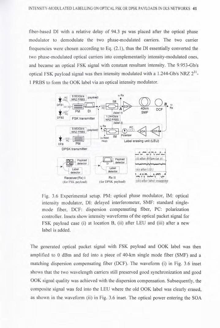
INTENSITY-MODULATED LABELLING ON OPTICAL FSK OR DPSK PAYLOADS IN OLS NETWORKS 41
fiber-based DI with a relative delay of 94.3 ps was placed after the optical phase
modulator to demodulate the two phase-modulated carriers. The two carrier
frequencies were chosen according to Eq. (2.1),thus the DI essentially converted the
two phase-modulated optical carriers into complementarily intensity-modulated ones,
and became an optical FSK signal with constant resultant intensity. The 9.953-Gb/s
optical FSK pay load signal was then intensity modulated with a 1.244-Gb/s N R Z 2 '-
1 PRBS to form the O O K label via an optical intensity modulator.
1 9 QAlfib/s , ' , 10 Rx
’ 母 纖 ⑵ ) „ I ( H ) n
^ ! P M DI : ^ ^ ^ e n r S M F 。。「
DFB2 ; FSK transmitter [ . J f g S J
j (label 2) •...�
1 疫 向
t r » ly ;Polarizer 1 — Q u a — " a n ™ — (10 Next ‘ ‘ PC I Hop) Label erasing unit (LEU)
D F B P M
D P S K transmitter [ 「-.厂
I Payload i [ r ~ \ | |""PayToad~|'i iuialk:释.m.(lU ML., 1-躯c斩」:. r oT LtectoLj; — 一 〜 一
. . . w OBPF , 1 ; ‘ : 、i-Labefl Label | (…allci.;LI!:U
detector 丨 L ^ l ; : 二….丨••_ : ‘
Receiver(Rx)丨 Rx i 1 i兮,
(for 1-SK payload) (for D P S K pay load) ..(.丨!1》”】1化她 胜 收
Fig. 3.6 Experimental setup. PM: optical phase modulator, IM: optical
intensity modulator, DI: delayed interferometer, SMF: standard single-
mode fiber, DCF: dispersion compensating fiber, PC: polarization
controller. Insets show intensity waveforms of the optical packet signal for
FSK payload case (i) at location B, (ii) after L E U and (iii) after a new
label is added.
The generated optical packet signal with FSK payload and O O K label was then
amplified to 0 d B m and fed into a piece of 40-km single mode fiber (SMF) and a
matching dispersion compensating fiber (DCF). The waveform (i) in Fig. 3.6 inset
shows thai the two wavelength carriers still preserved good synchronization and good
O O K signal quality was achieved with the dispersion compensation. Subsequently, the
composite signal was fed into the LEU where the old O O K label was clearly erased,
as shown in the waveform (ii) in Fig. 3.6 inset. The optical power entering the S O A
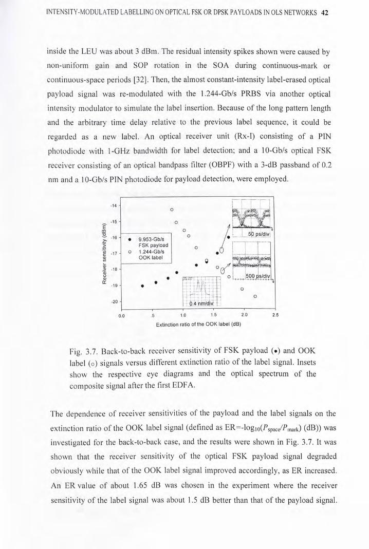
INTENSITY-MODULATED LABELLING ON OPTICAL FSK OR DPSK PAYLOADS IN OLS NETWORKS 42
inside the LEU was about 3 dBm. The residual intensity spikes shown were caused by
non-uniform gain and SOP rotation in the SOA during continuous-mark or
continuous-space periods [32]. Then, the almost constant-intensity label-erased optical
payload signal was re-modulated with the 1.244-Gb/s PRBS via another optical
intensity modulator to simulate the label insertion. Because of the long pattern length
and the arbitrary time delay relative to the previous label sequence, it could be
regarded as a new label. An optical receiver unit (Rx-I) consisting of a PIN
photodiode with 1-GHz bandwidth for label detection; and a 10-Gb/s optical FSK
receiver consisting of an optical bandpass filter (OBPF) with a 3-dB passband of 0.2
nm and a 10-Gb/s PIN photodiode for payload detection, were employed.
I ~ ~ i 丨―.厂;
°。 , 國 CD O / ‘ 1 丨 jK -16 • 9.953-Gb/s / •
I F S K payload 。 人 \ \
w -17. o 1.244-Gb/s i
i O O K label ^ -18- • Cf i i .
-19 - • . i Ar i[ t I A • , -..<«'. -I t - I • •
务 :QA prnm ‘ 1 — ~ 1 1 1
0.0 .5 1.0 1.5 2.0 2.5
Extinction ratio of the O O K label (dB)
Fig. 3.7. Back-to-back receiver sensitivity of FSK payload (•) and O O K
label (o) signals versus different extinction ratio of the label signal. Insets
show the respective eye diagrams and the optical spectrum of the
composite signal after the first EDFA.
The dependence of receiver sensitivities of the payload and the label signals on the
extinction ratio of the O O K label signal (defined as ER=-logio(Pspac(/^mark) (dB)) was
investigated lor the back-to-back case, and the results were shown in Fig. 3.7. It was
shown thai the receiver sensitivity of the optical FSK payload signal degraded
obviously while that of the O O K label signal improved accordingly, as ER increased.
An ER value of about 1.65 dB was chosen in the experiment where the receiver
sensitivity of the label signal was about 1.5 dB better than that of the payload signal.

INTENSITY-MODULATED LABELLING ON OPTICAL FSK OR DPSK PAYLOADS IN OLS NETWORKS 43
Fig. 3.8 shows the bit error rate (BER) measurements for the back-to-back case, after
40-krn transmission, and after all-optical label swapping, measured at locations A, B,
and C in Fig.3.6, respectively. It was shown that both of the label and the payload
signals experienced around 1-dB power penalty after 40-km transmission, which was
possibly caused by the relatively large frequency spacing of the optical FSK signal
and the dispersion slope mismatch between the S M F and the DCF. A power penalty of
less than 0.2 dB for both the payload and the renewed label signals after one stage of
all-optical label swapping was mainly attributed to the small amount of ASE noise in
the SO A. Moreover, such very small power penalty revealed the robustness of our
proposed LEU and the potential cascadability of the label switching networks. In a
typical OLS networks, the label has to be erased and renewed at each network node.
As the spacing of the network nodes is usually 40-60 km, our experimental results
showed that the label, though with such a relatively small ER (< 2dB), could still be
transmitted with good performance provided that there was proper dispersion
compensation.
10.3 ‘ ‘ Label B2B
• Labe丨40km V • Label S w p V . • Payload B2B
vP 51 \ \ • \ 、 Payload 40km 10'" \ V \ \ \ \ • Payload Swp
S \ \ FSK 10-6 . label \ \ X \ \ \ payload
-21 -20 -19 -18 -17 -16
Average received power (dBm)
Fig. 3.8. B E R measurements of FSK payload and O O K label signals for
three cases: back-to-back (B2B), after 40-km transmission, and after label
swapping (Swp).
By using the same experimental setup with the optical D P S K transmitter and the
respective optical receiver unit (Rx-Il), as shown in Fig. 3.6, the transmission and
label swapping performance of employing optical D P S K payload was also

INTENSITY-MODULATED LABELLING ON OPTICAL FSK OR DPSK PAYLOADS IN OLS NETWORKS 44
investigated. The generated optical DPSK payload signal was modulated by the
optical intensity modulator for encoding the 1.244-Gb/s O O K label at an ER value of
1.5 dB. Similar to the case of optical FSK payload, the system performance of using
DPSK signal greatly depended on the ER, which could be discovered from Fig. 3.9.
At the ER value of 1.5 dB, almost the same receiver sensitivity of-18.4 dBm for both
the payload and the label signals in the back-to-back case was achieved as shown in
Fig. 3.10. After 40-km transmission, either the payload or the label signal suffered
from less than 1-dB power penalty at BER=10"^ The slightly different slopes of the
curves might be caused by the different noise characteristics and the induced signal-
to-noise ratios before and after transmission, as well as after label swapping. Nearly
no additional penalty was induced to the O O K label signal after the all-optical label
swapping, which implied that the constant-intensity property of the optical D P S K
payload signal was kept better than that of the optical FSK payload case. On the other
hand, however, the optical DPSK payload signal suffered from a power penalty of
about 1 dB after the all-optical label swapping. This might be attributed to the fact that
the mark and the space levels of the O O K label experienced different gain in the S O A
inside the LEU, due to the variation of the carrier density [33], which in turn induced
different phase change to the optical DPSK payload signal. Nevertheless, as the
extinction ratio of the label signal was maintained at a low value, such degradation
was small and tolerable.
-17.0 1 —
-17.5 -
-p ° • 9.952-Gb/s
(I -18.0 - • D P S K payload
2 . • o 1.244-Gb/s
圣—18.5 - 争 O O K label
: ! • o ^ -19.0 -① w 0 -19.5 ->
'53 o ^ -20.0 -
(T o
-20.5 -
O -210 1 1 1 1 1
0.5 1.0 1.5 2.0 2,5 3.0 3.5
Extinction ratio of the O O K label (dB)
Fig. 3.9. Back-to-back receiver sensitivity of D P S K payload (•) and O O K
label (o) signals versus different extinction ratio of the label signal.
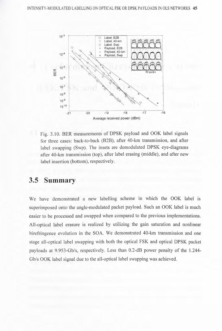
INTENSITY-MODULATED LABELLING ON OPTICAL FSK OR DPSK PAYLOADS IN OLS NETWORKS 45
10.3 “ ‘ 〇 Label, B 2 B ‘
• X Payload, B 2 B 卜,•'"•"‘?"!..:"" •"‘
-21 才o" -19 -18 -17 -16
Average received power (dBm)
Fig. 3.10. B E R measurements of D P S K payload and O O K label signals
for three cases: back-to-back (B2B), after 40-km transmission, and after
label swapping (Swp). The insets are demodulated D P S K eye-diagrams
alter 40-km transmission (top), after label erasing (middle), and after new
label insertion (bottom), respectively.
3.5 Summary
W e have demonstrated a new labelling scheme in which the O O K label is
superimposed onto the angle-modulated packet payload. Such an O O K label is much
easier to be processed and swapped when compared to the previous implementations.
All-optical label erasure is realized by utilizing the gain saturation and nonlinear
birefringence evolution in the SOA. W e demonstrated 40-km transmission and one
stage all-optical label swapping with both the optical FSK and optical D P S K packet
payloads al 9.953-Gb/s, respectively. Less than 0.2-dB power penalty of the 1.244-
Gb/s O O K label signal due to the all-optical label swapping was achieved.
PERFORMANCE CHARACTERIZATION OF THE ASICI^SK AND ASK/DPSK ORTHOGONAL SIGNALS 46
4 Performance Characterization of the
ASK/FSK and ASK/DPSK Orthogonal
Signals
4.1 Introduction and Formulation
In optical digital communication systems, orthogonal modulation constructs a special
formal in which a light wave simultaneously carries two different sets of data. Each
set of data is usually either intensity-modulated or angle-modulated, respectively. It
has been widely used in optical networks to facilitate various functionalities, including
data controlling and supervision [3], optical packet labelling [27], etc. In these two
cases the supervisory/header/label data is much slower than the packet payload. For
instance, the payload is at 10 Gb/s while the label is at 2.5 Gb/s or even down to tens
ofMb/s.
In this chapter, we investigate two orthogonal modulation schemes, namely ASK/FSK
and ASK/DPSK, that is, the relatively low-speed optical amplitude-shift-keying (ASK)
signal is superimposed onto the high-speed optical FSK or DPSK payload with
constant intensity. Both of them can be received through direct detection, using
receiver structures shown in Figs. 4.1 and 4.2. The optical A S K signal can be directly
detected by a conventional AC-coiipled square-law detector while the optical FSK or
D P S K signal is demodulated by an optical filter or an optical delay interferometer (DI)
before detection, respectively. For such orthogonal modulation schemes, the qualities
of both the A S K and the optical FSK or D P S K signals strongly depend on the
extinction ratio (ER) of the optical A S K signal. In such applications, the extinction
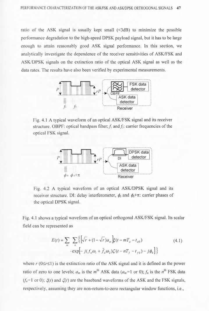
PERFORMANCE CHARACTERIZATION OF THE ASICI^SK AND ASK/DPSK ORTHOGONAL SIGNALS 47
ratio of the A S K signal is usually kept small (<3dB) to minimize the possible
performance degradation to the high-speed DPSK payload signal, but it has to be large
enough to attain reasonably good A S K signal performance. In this section, we
analytically investigate the dependence of the receiver sensitivities of ASK/FSK and
ASK/DPSK signals on the extinction ratio of the optical A S K signal as well as the
data rates. The results have also been verified by experimental measurements.
t ~ I ~ I ~ L . i J ^ G FSK data |i p \ T ,) I r ^ ^ ^ de tec to r l i ^ i
i V j A S K da ta j !:1 I I de tec to r j 丨 力 Rece ive r
Fig. 4.1 A typical waveform of an optical ASK/FSK signal and its receiver
structure. OBPF: optical bandpass filter; /,' and力:carrier frequencies of the
optical FSK signal.
个 I I L I | J ~ l | | D P S K d a t a | i IrP detector |
i V i A S K da ta i iJ I I de tec to r ;
小 、 、 於 � Receive}" ‘
Fig. 4.2 A typical waveform of an optical ASK/DPSK signal and its
receiver structure. DI: delay interferometer,於)and 办+7i: carrier phases of
the optical D P S K signal.
Fig. 4.1 shows a typical waveform of an optical orthogonal ASK/FSK signal. Its scalar
field can be represented as
(4.1) … n
where r (0<r<l) is the extinction ratio of the A S K signal and it is defined as the power
ratio of zero to one levels; a,„ is the w") A S K data (c/,„=l or 0); is the FSK data
(八7=1 or 0); {i) and ({I) are the baseband waveforms of the A S K and the FSK signals,
respectively, assuming they are non-relurn-to-zero rectangular window functions, i.e.,

PERFORMANCE CHARACTERIZATION OF THE ASICI^SK AND ASK/DPSK ORTHOGONAL SIGNALS 48
0, else [0, else
where I) is the power of the one level; T�and 7} are the bit periods of the A S K and the
FSK signals, respectively; /“o and ijo are relative time delays, for the A S K and the FSK
signals, respectively.
In Fig. 4.2, a typical temporal waveform of an optical orthogonal ASK/DPSK signal is
shown. Its scalar field can be represented as
么,⑴=Z I; { + (1 - 而 〜 h ' - - /“�) m n .exp[- JTT d„at - nT, - U )]exp[- jcot - jc^ ] } (々 .二)
where r (0<r< 1) is the extinction ratio of the optical A S K signal and it is defined as
the power ratio of zero to one levels; a„, is the A S K data («,„=! or 0); d„ is the “山
precoded DPSK data id„=\ or 0);《(/) and C(0 are the baseband waveforms of the
A S K and the DPSK signals, respectively, assuming they are non-return-to-zero
rectangular window functions, i.e.,
IJp o</ < r fi, o</<r^/
where I) is the power of the one level; J\, and Td are the bit periods of the A S K and the
DPSK signals, respectively; and /"() are relative time delays, for the A S K and the
DPSK signals, respectively.
4.2 Theoretical Analysis
4.2.1 Optical ASK performance in orthogonal signals
In ASK/FSK or ASK/DPSK orthogonal signals, as both the optical FSK or the optical
DPSK payload has constant intensity, the optical A S K signal superimposed on the
payload can be extracted and delected by an AC-coiipled optical receiver; thus it has
the same receiver performance as the typical optical A S K signal. In [39], the error
probability of an optical A S K signal has been derived based on the fact that thermal

PERFORMANCE CHARACTERIZATION OF THE ASICI^SK AND ASK/DPSK ORTHOGONAL SIGNALS 49
noise dominates receiver performance when the received power is relatively small,
and this can be well described by Gaussian statistics:
歸 b 二 Ic^r/cl—1 where Q = — ~ — , I\ and k are the mark and the space levels “ 2 [ 4 2 ) … + 〜
respectively, and (Ji = ob= cry are the thermal noise in the p-i-n receiver.
As r =尸()/ /)| ; and using the definition of the receiver sensitivity
=(尸I + /)•) / 2 = (1 + r)/V 2,the parameter 0 can be given by:
。一 ^ 一 {’ I /(1 + r) (4.3)
‘ CT 丨 + cr(, 2ov
where R is the receiver responsivity. By substituting the expression of or into Eq.
(4.3), gives:
- a U k J F , B , f \ ^ A (4.4)
^ ^ “ Ro i K , u - j "
“ is regarded as the receiver sensitivity when Q丨=6.00 such that the error
probability of the optical A S K signal prob。’" 二 erfc(a /V2) = 10"'.
Therefore, at a fixed ASK/DPSK bit rate, the optical A S K label, having an extinction
ratio of r. has a receiver sensitivity (at probe.a=\0' ), P,,,,, ’ given by
= C,. , , .=o(dBm) + 10 l o g � (4.5)
At a certain extinction ratio, the receiver sensitivity of the A S K label signal is
approximately proportional to the square root of its bit rate.
4.2.2 Optical FSK performance in ASK/FSK signals
To detect the FSK data, an optical ASK/FSK signal is fed into an optical bandpass
filter before the photodiode. One frequency carrier is filtered out and the other one is

PERFORMANCE CHARACTERIZATION OF THE ASICI^SK AND ASK/DPSK ORTHOGONAL SIGNALS 50
converted into an intensity modulated carrier. And the output power of the
demodulated FSK bit at its sampling point is:
P" = + (1 - ^ f r ) a „ , \ f P • exp[- jf,�(0\(/ — nT,. -1丨々)-y^o.
The values ol、/)„ can be determined by substituting all possible values of c/„, andinto
Eq. (4.6), which can be formed as Table 4.1:
Table 4.1: Possible output power levels of an ASK/FSK signal from the OBPF
A S K a,n FSK./;, Probability of occurrence Output power from OBPF !
I 0 or 1 0 j P\ =0
II 0 1 ^ Pii = rP
III I 1 1 P\\\ = P 4
Assuming Gaussian noise statistics, the error probability of the demodulated optical
FSK signal is formulated as
probe�丨=prob{0) • pwh{\ | 0 ) + prob{\). pn)h{Qi 11)
1 1 ‘、「//)-O"! 1 1 f「,,/?尸一/"]丄 1 1 J r P - I , , ] (4.7) = — — e r i c ~ + ——erfc p""“- +---erfc —j=~'丄
2 2 V2ct, 4 2 V2cj„ 4 2 V2(j,„ — ‘ -J L J I— —
where lo is the decision threshold value, R is the photodiode's responsivity, cr, (for
/G{I, II,...,111}) is the receiver noise in each case, and erfc[.] is the complementary
error function.
To find the minimum error probability, we let dprob^ ^ / d l = 0. This equation has
no closed-form solution; thus requires numerical computation to obtain Id. Using this
//J), the corresponding error probability probej can be computed. With probej = 1

PERFORMANCE CHARACTERIZATION OF THE ASICI^SK AND ASK/DPSK ORTHOGONAL SIGNALS 51
the received optical power (receiver sensitivity) is derived with respect to the receiver
noise. Based on numerical solutions, the receiver sensitivity of the optical FSK signal
is plotted in Fig. 4.3. As the extinction ratio in dB scale (ERdB = -101og,or) of the ASK
signal increases, the intensity fluctuation at the FSK signal envelope is enhanced, thus
the FSK signal is further degraded.
-16r I
-16 .5 |
E 17 Z g l 7 . 5 /
I 18 / •运-18.5 丨
0) ‘ Z -19, Z
> i
^ -20 K
-20.5i
I々q - - 1 飞 — ‘ 3 '4 5 6
Extinction Ratio of the ASK signal (dB)
Fig. 4.3 FSK receiver sensitivity in an optical ASK/FSK signal
4.2,3 Optical DPSK performance in ASK/DPSK signals
For the orthogonal ASK/DPSK signal, an optical DI with a relative arm delay of T^ is
used to demodulate the DPSK data. The DI output from one port is:
n
E_ (/) = • [(1 / 2 ) E { I ) + (1 / 2 ) E { t - T,)] (4.8)
The output power of the demodulated DPSK bit at its sampling point is:
p " = 去 + — 厂 一 " + 去 + —
= + (1 - + + 尸 (4.9)
+ + (1 — V7vv〃]. [V7 + (1 — V^K„,〃_,> • e-一“"~'丨丨-、、
where c!川is the A S K data being superimposed on the DPSK bit, at the sampling
point. Note thai a„,,„ and an,,n.\ may stand for the same or adjacent A S K bits. By

PERFORMANCE CHARACTERIZATION OF THE ASICI^SK AND ASK/DPSK ORTHOGONAL SIGNALS 52
considering all possible combinations of the A S K bits («„,,,„ “,„,„-i) and the DPSK bits
、e,_,,+‘“,-、、),the output powers (/),,) of the demodulated D P S K bit are tabulated
in Table 1, together with their probability of occurrence, assuming that ones and zeros
are equally probable. The derivation of prob\\\ is given below, and the others can be
obtained similarly.
— 丨 丨 丨 = p r ( M c 、 " = 0, 丨 = 0 , e - — " < 、 、 = + 1 }
=[prob{a,„^„ = 0, “„,’,卜 1 = 0}] • p w b � e - — " < � �= +1}
=[proh{a„, „ equals 0 and c/,„,卜丨 at the previous A S K bit period and it equals 0 too}
+ prob{u", " equals 0 and at the same A S K bit period with -(1/2)
= l/4-(l/8)(r,/7;)
Table 4.2: Output power of demodulated ASK/DPSK signal
A S K OPSK
, ) Probability of occurrence Output power from DI
, 0 , 0 or 丄—丄.Z^ =0
_ _ 2 4 7;
II O,lor l A 丄 +丄 P —丄 V ^ P 1,0 " 4 4 2
i V T , III 0 , 0 P\\\ = rP
+1 j j — ^
V 1 1 = P , 4 8 T
li!
Assuming Gaussian noise statistics, the error probability of the demodulated DPSK
signal is:

PERFORMANCE CHARACTERIZATION OF THE ASIC/PSK AND ASK/DPSK ORTHOGONAL SIGNALS 53
probe J = prob{0). prob{\ | 0) + prob{\) • prob{0 丨 1)
= f 丄 」 . 年 + f 丄 • 犯 U 4 T j 2 L V2C7, J 1 4 r j 2 L _
+ f i 」 . Z 4 i e i . t 、 c h ^ l + f i . 4 i e i . 4 ¥ l (4,10) 1,4 8 T j 2 L V 2 ( j , „ 」 ( 4 7 J 2 _
J i - i . Z ^ U e J ^ '
U s T J 2 L 彻 V .
where //) is the decision threshold, R is the photodiode's responsivity, cr, (for ie{\,
11,...’V}) is the receiver noise in each case, and erfc[-] is the complementary error
function.
In such applications of optical orthogonal ASK/DPSK signals [3], the payload has a
few limes higher speed than the supervisory/label data. For instance, D P S K payload at
10-Gb/s and A S K label at 2.5-Gb/s or lower in label switching networks. Thus, in our
analysis, we assume Moreover, with small received power at the receiver,
thermal noise dominates, thus we can assume c7,(for /e{l’ n,’..,V}) 二cPr. Besides, for
a certain range of the E R values, which is found to be 0.63<r<0.95, or 0.2dB<ERdB<
2dB at the optimal decision threshold h obtained below,
comparable with erfc[(/,) - RPu)/[^cj,)] ; Qrfc[{RP,y - 1 丨 難 4 and
Q v k [ ( R P , - I i , ) / y 2 ( J i ) ] are smaller than erfc[(7?P,„ - / J / ( V 2 a , ) ] b y a f e w orders of
magnitude. Hence, under the above conditions, the first two terms can be combined
and the 4山,5山 terms can be neglected in Eq. (4.10), which can then be simplified as:
一 H e 长 ] + H e 4 劑 (4.11)
Let dpn)beJdh=〜 we have found that the optimal value of h can be approximated
by {rPR/2). for p r o l h j ^ At this optimal h , we have
— ‘ , ’ " 〜 〜 H 暑卜 (4.12)
For proh^., = 10—‘), Q:, -5.95, i.e. PR = \ \ . 9 g , /r .

PERFORMANCE CHARACTERIZATION OF THE ASICI^SK AND ASK/DPSK ORTHOGONAL SIGNALS 54
From the power and the probability of each case in Table 1,the average received
power of the demodulated DPSK signal equalsP^, =(r + l)?/4. Together with Eq.
Q —
(4.12). the receiver sensitivity (at probe,cr^Qi' ), , of the demodulated DPSK
signal is given by
一 _ , + i (4.13) Pr“. “丨(dBm) = P … ( d B m ) + 101og,„ —
2r
Using Eq. (4.13) and supposing the receiver sensitivity for ERdB=0 is -19.2 dBm, the
receiver sensitivity of the 10-Gb/s D P S K data in ASK/DPSK signals was drawn in Fig.
4.4 as the black solid line. W e have also numerically computed the relation between
the receiver sensitivity of the D P S K data and the extinction ratio of the A S K data,
according to Eq. (4.10). It shows that the simplified analytical curve (solid line)
almost coincides with the numerically calculated curves for different A S K bit rates,
for ER<3.5 dB, which attests the simplifications and assumptions in our analytical
model are reasonably valid. When ERdB increases beyond this value, the error between
the simplified analytical curve and the numerical solved curve starts accretion, owing
to the non-negligible augment of the abridged terms from Eq. (4.10) to Eq. (4.11). W e
can see that the D P S K signals have almost the same performance with different A S K
bit rates. And for ER>3 dB, the demodulated D P S K signal with higher A S K bit rate
has slightly more degraded receiver sensitivity.
丨 , -16 丨 ! / (Area zoonieci-in)
二 -18 2-16.6. , , , Z (U ^ ^ 0)
^ X T ^ DPSK ttr<2.5Gb/r K (ana) ~ ^ .19 " D P S K with 2.5-Gb/s ASK (num) g-16 8 a: ^ I - -…DP S K with 1.25-Gb/s ASK (num) ^ ^ ^
j-.十-DPSKwith 1-Gb/s ASK(nunn) / :_ [ana=an icaLni =nur iyJ}J ^ ^
i 2 3 ^ 6 3 . 8 A 2 4 :4 4 : 6 Extinction Ratio of the ASK signal (dB) Extinction Ratio of the ASK signal (dB)
Fig. 4.4 The D P S K receiver sensitivity versus A S K extinction ratio
obtained through simplified analytical (solid line) and numerical (other
lines) approaches
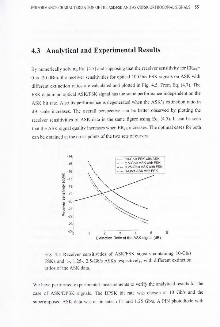
PERFORMANCE CHARACTERIZATION OF THE ASICI^SK AND ASK/DPSK ORTHOGONAL SIGNALS 55
4.3 Analytical and Experimental Results
By numerically solving Eq. (4.7) and supposing that the receiver sensitivity for ERdB =
0 is -20 dBm, the receiver sensitivities for optical 10-Gb/s FSK signals on A S K with
different extinction ratios are calculated and plotted in Fig. 4.5. From Eq. (4.7), The
I'SK data in an optical ASK/FSK signal has the same performance independent on the
A S K bit rate. Also its performance is degenerated when the ASK's extinction ratio in
dB scale increases. The overall perspective can be better observed by plotting the
receiver sensitivities of A S K data in the same figure using Eq. (4.5). It can be seen
that the A S K signal quality increases when ERdB increases. The optimal cases for both
can be obtained at the cross points of the two sets of curves.
-14|
! — 10-Gb/s FSK with A S K _15 \ 2.5-Gb/s A S K with FSK
\ 1.25-Gb/s A S K with FSK -16 .、 ••…1-Gb/s A S K with FSK
一 \ • —
E 丨 , 、 � • ^
f - 1 8 \
I - i 9 i _ ^ A r ^ 、 . 、
1 I .••々 、、 、、、、 8 -21 、 > , 、 ’、 (U 、?、
-23 I
- 2 4 、 r J-.— .— 3 ' 4 r “ 6
Extinction Ratio of the ASK signal (dB)
Fig. 4.5 Receiver sensitivities of ASK/FSK signals containing 10-Gb/s
FSKs and 1-, 1.25-, 2.5-Gb/s ASKs respectively, with different extinction
ratios of the A S K data.
W e have performed experimental measurements to verify the analytical results for the
case of ASK/DPSK signals. The DPSK bit rate was chosen at 10 Gb/s and the
superimposed A S K data was at bit rates of 1 and 1.25 Gb/s. A PIN photodiode with
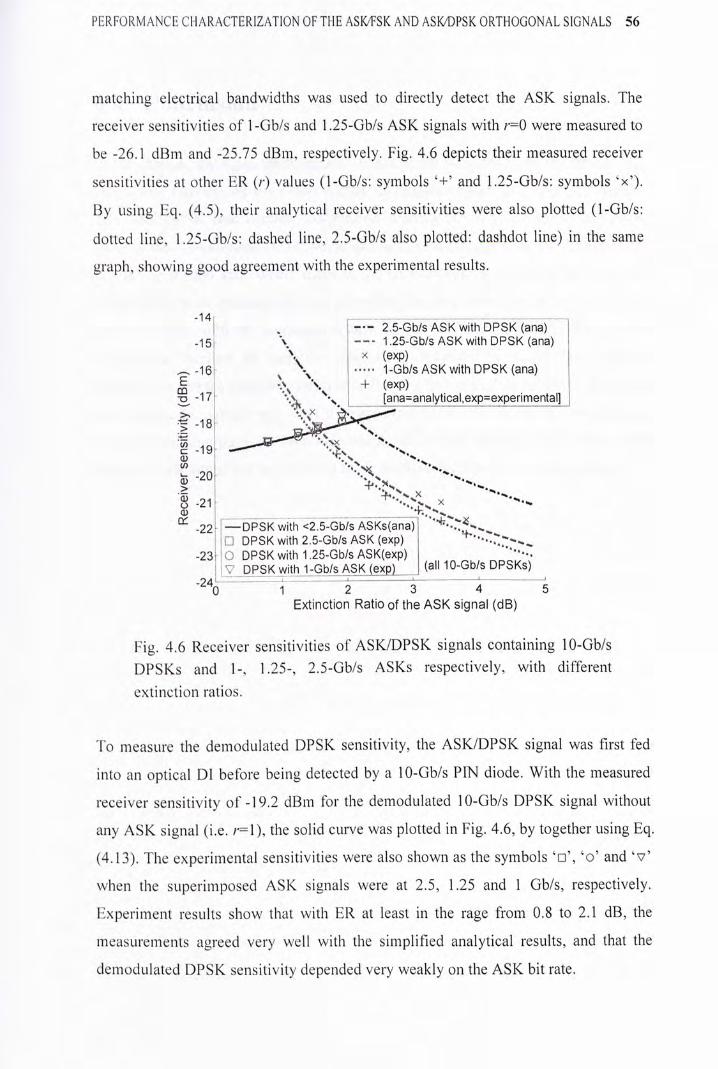
P E R F O R M A N C E C H A R A C T E R I Z A T I O N OF T H E ASICI^SK A N D ASK/DPSK O R T H O G O N A L S I G N A L S 5 6
matching electrical bandwidths was used to directly detect the A S K signals. The
receiver sensitivities of 1-Gb/s and 1.25-Gb/s A S K signals with r=0 were measured to
be -26.1 d B m and -25.75 dBm, respectively. Fig. 4.6 depicts their measured receiver
sensitivities at other ER (/•) values (1-Gb/s: symbols ‘+’ and 1.25-Gb/s: symbols 'x').
By using Eq. (4.5), their analytical receiver sensitivities were also plotted (1-Gb/s:
dotted line, 1.25-Gb/s: dashed line, 2.5-Gb/s also plotted: dashdot line) in the same
graph, showing good agreement with the experimental results.
-14 • 厂二2—5—-Gb/s A S K with D P S K ( a n a ) —
- 1 5 \ --- 1.25-Gb/s A S K with D P S K (ana)
\ X (exp)
_ -16- \ ..…1-Gb/s A S K with D P S K (ana)
E >’〉、.、 + (exp)
; - 1 7 - 、.、 [ana=analytical,exp=experimental]
� \ � � � * �
^ -21 ��� ^ - 2 2 p ^ D P S K with <2.5-Gb7s A S K s ( a 7 i ^
• D P S K with 2.5-Gb/s A S K (exp)
-23 -〇 D P S K with 1.25-Gb/s ASK(exp)
V D P S K with 1-Gb/s A S K (exp) (a丨丨 10-Gb/s D P S K s )
-24、 r - 2 3 ' 4 5
E x t i n c t i o n R a t i o o f t h e A S K s i g n a l (d已)
Fig. 4.6 Receiver sensitivities of ASK/DPSK signals containing 10-Gb/s
DPSKs and 1-, 1.25-, 2.5-Gb/s ASKs respectively, with different
extinction ratios.
To measure the demodulated D P S K sensitivity, the ASK/DPSK signal was first fed
into an optical DI before being detected by a 10-Gb/s PIN diode. With the measured
receiver sensitivity of -19.2 dBm for the demodulated 10-Gb/s D P S K signal without
any A S K signal (i.e. /•=!), the solid curve was plotted in Fig. 4.6, by together using Eq.
(4.13). The experimental sensitivities were also shown as the symbols ‘•,,'o' and ‘•’
when the superimposed A S K signals were at 2.5, 1.25 and 1 Gb/s,respectively.
Experiment results show that with ER at least in the rage from 0.8 to 2.1 dB, the
measurements agreed very well with the simplified analytical results, and that the
demodulated D P S K sensitivity depended very weakly on the A S K bit rate.

PERFORMANCE CHARACTERIZATION OF THE ASICI^SK AND ASK/DPSK ORTHOGONAL SIGNALS 57
4.4 Conclusion
In the chapter, the signal performance of both of the ASK/FSK and the ASK/DPSK
orthogonal formats has been theoretically investigated based on probability models.
The ASK/DPSK case is more complicated in terms of analysis than the ASK/FSK
case, as the demodulated DPSK signal has more possible power levels. However, by
neglecting several subordinate terms in the error probability function, an analytical
solution has been obtained from the simplified function, which has also been proven
to be agreeing with the numerical results as well as the experimental results. The
calculations implied an analytical relationship between the ASK/DPSK receiver
sensitivities and the extinction ratios as well as the bit rates of the optical A S K signal,
and the results agreed well with the experimental results. Using this analysis, an
optimal operating point for both the optical A S K signal and the optical FSK or the
optical D P S K signal can be predicted easily and thus facilitates the system design.

CONCLUDING REMARKS 58
5 Summary
5.1 Thesis Summary
In this thesis, we have proposed and thoroughly investigated several applications of
optical FSK in lightwave systems.
Providing some background. Chapter 1 introduces the basic concepts and the related
techniques, especially in the optical FSK transmitters and receivers that are employed
in our investigations in later chapters. The concepts of CLS W D M - P O N and OLS
network have also been introduced.
In Chapter 2, the optical FSK format is selected as the downstream optical modulation
formal to facilitate upstream re-modulation in CLS PON. With the constant intensity
property of the downstream FSK signal, the upstream transmitter at the O N U can
simply be realized by directly intensity-modulating the upstream data onto the
downstream FSK signal. PONs using different downstream FSK transmitters have
been investigated and demonstrated. Good transmission performance of both the
downstream and the upstream signal has been achieved. The performance of the
newly proposed optical FSK transmitter based on phase modulation together with the
CLS P O N has also been experimentally studied.
Another application of the optical FSK modulation format in OLS networks have been
proposed and studied in Chapter 3. A new labelling scheme using OOK-modulated
optical labels on the optical FSK payloads is proposed and demonstrated. The all-
optical label swapping was realized using the nonlinear properties in semiconductor
optical amplifiers (SOA). Besides, another common angle modulation format, DPSK,
can also be employed as the payload format and this case was also experimentally
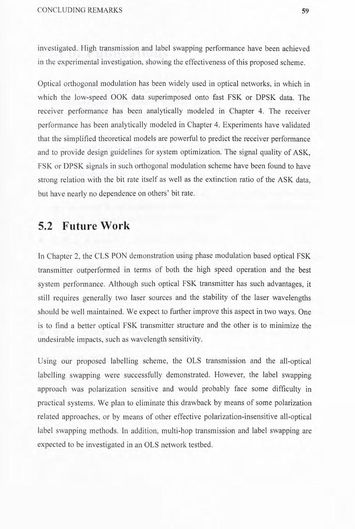
CONCLUD ING REMARKS 59
investigated. High transmission and label swapping performance have been achieved
in the experimental investigation, showing the effectiveness of this proposed scheme.
Optical orthogonal modulation has been widely used in optical networks, in which in
which the low-speed O O K data superimposed onto fast FSK or D P S K data. The
receiver performance has been analytically modeled in Chapter 4. The receiver
performance has been analytically modeled in Chapter 4. Experiments have validated
that the simplified theoretical models are powerful to predict the receiver performance
and to provide design guidelines for system optimization. The signal quality of ASK,
FSK or DPSK signals in such orthogonal modulation scheme have been found to have
strong relation with the bit rate itself as well as the extinction ratio of the A S K data,
but have nearly no dependence on others' bit rate.
5.2 Future Work
In Chapter 2, the CLS P O N demonstration using phase modulation based optical FSK
transmitter outperformed in terms of both the high speed operation and the best
system performance. Although such optical FSK transmitter has such advantages, it
still requires generally two laser sources and the stability of the laser wavelengths
should be well maintained. W e expect to further improve this aspect in two ways. One
is to find a better optical FSK transmitter structure and the other is to minimize the
undesirable impacts, such as wavelength sensitivity.
Using our proposed labelling scheme, the OLS transmission and the all-optical
labelling swapping were successfully demonstrated. However, the label swapping
approach was polarization sensitive and would probably face some difficulty in
practical systems. W e plan to eliminate this drawback by means of some polarization
related approaches, or by means of other effective polarization-insensitive all-optical
label swapping methods. In addition, multi-hop transmission and label swapping are
expected to be investigated in an OLS network testbed.
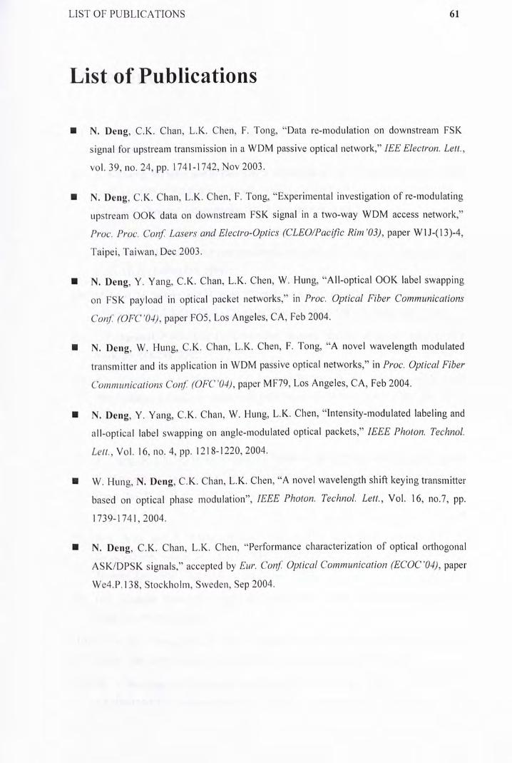
LIST OF PUBLICATIONS 61
List of Publications
• N . Deng, C.K. Chan, L.K. Chen, F. Toiig, "Data re-modulation on downstream F S K
signal for upstream transmission in a W D M passive optical network," lEE Electron. Lett.,
vol. 39,110. 24, pp. 1741-1742’ N o v 2003.
• IN. Deng, C.K. Chan, L.K. Chen, F. Tong, "Experimental investigation of re-modulating
upstream O O K data on downstream FSK signal in a two-way W D M access network,"
Proc. Proc. Conf. Lasers and Electro-Optics (CLEO/Pacific Rim '03), paper WlJ-(13)-4,
Taipei, Taiwan, Dec 2003.
• N . Deng, Y . Yang, C.K. Chan, L.K. Chen, W . Hung, "All-optical O O K label swapping
on F S K payload in optical packet networks," in Proc. Optical Fiber Commumcatiom
Conf. (OFC '04), paper F05, Los Angeles, C A , Feb 2004.
• IN. Deng, W . Hung, C.K. Chan, L.K. Chen, F. Tong, ‘‘A novel wavelength modulated
transmitter and its application in W D M passive optical networks," in Proc. Optical Fiber
Communicalions Conf. (OFC04), paper M F 7 9 , Los Angeles, C A , Feb 2004.
• N . Deng, Y . Yang, C.K. Chan, W . Hung, L.K. Chen, 'intensity-modulated labeling and
all-optical label swapping on angle-modulated optical packets," IEEE Photon. Technol.
Led., Vol. 16, no. 4, pp. 1218-1220, 2004.
• W . Hung, N. Deng, C.K. Chan, L.K. Chen, "A novel wavelength shift keying transmitter
based on optical phase modulation", IEEE Photon. Technol. Lett., Vol. 16, no.7, pp.
1739-1741,2004.
• N . Deng, C.K. Chan, L.K. Chen, “Perfoniiance characterization of optical orthogonal
A S K / D P S K signals;' accepted by Eur. Conf. Optical Communication (ECOC'04), paper
We4.P.138, Stockholm, Sweden, Sep 2004.
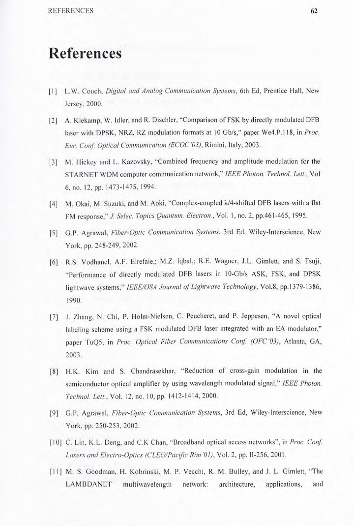
REFERENCES 62
References
[1J L . W . Couch, Digital and Analog Communication Systems, 6th Ed, Prentice Hall, N e w
Jersey, 2000.
[2] A . Klekamp, W . Idler, and R. Dischler, “Comparison of F S K by directly modulated D F B
laser with D P S K , N R Z , R Z modulation formats at 10 Gb/s," paper We4.P.118, in Proc.
Eur. Conf: Optical Comnnmicalion (ECOC'03), Rimini, Italy, 2003.
[3J M . Mickey and L. Kazovsky, "Combined frequency and amplitude modulation for the
S T A R N E T W D M computer communication network," IEEE Photon. Technol. Lett., Vol
6, no. 12, pp. 1473-1475, 1994.
[4] M . Okai, M . Suzuki, and M . Aoki, "Complex-coupled 人/4-sliifted D F B lasers with a flat
F M response," J. Selec. Topics Quantum. Electron., Vol. 1, no. 2, pp.461-465, 1995.
[5] G.P. Agrawal, Fiber-Optic Commimicalion Systems, 3rd Ed, Wiley-Interscience, N e w
York, pp. 248-249, 2002.
[6] R.S. Vodhanel, A.F. Elrefaie,; M.Z. Iqbal,; R.E. Wagner, J丄.Gimlett, and S. Tsiiji,
"Performance of directly modulated D F B lasers in 10-Gb/s A S K , F S K , and D P S K
lightwave systems," lEEE/OSA Journal of Lightwave Technology, Vol.8, pp.1379-1386,
1990.
[7] J. Zhang, N . Chi, P. Holm-Nielsen, C. Peucheret, and P. Jeppesen, "A novel optical
labeling scheme using a F S K modulated D F B laser integrated with an E A modulator,"
paper T u Q S , in Proc. Optical Fiber Commimicatiom Conf: {OFC'03), Atlanta, G A ,
2003.
[8] H.K. K i m and S. Chandrasekhar, "Reduction of cross-gain modulation in the
semiconductor optical amplifier by using wavelength modulated signal," IEEE Photon.
Technol. Le//., Vol. 12,no. 10, pp. 1412-1414, 2000.
[9] G.P. Agrawal, Fiber-Optic Comiinmication Systems, 3rd Ed, Wiley-Interscience, N e w
York, pp. 250-253, 2002.
110] C. Lin, K丄.Deng, and C.K Chan, “Broadband optical access networks", in Proc. Conf.
Lasers ami Electro-Optics (CLEO/Pacific Rim '01), Vol. 2, pp. 11-256, 2001.
[llj M . S. G o o d m a n , H. Kobrinski, M . P. Vecchi, R. M . Bulley, and J. L. Gimlett, “The
L A M B D A N E T multiwavelength network: architecture, applications, and
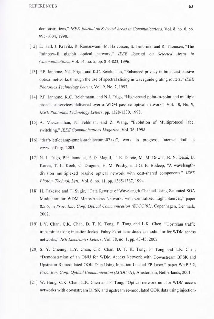
REFERENCES 63
demonstrations," IEEE Journal on Selected Areas in Communications, Vol. 8, no. 6, pp.
995-1004, 1990.
[12] E. Hall, J. Kravitz, R. Ramaswami, M . Halvorson, S. Tenbrink, and R. Thomsen, "The
Rain bow-11 gigabit optical network," IEEE Journal on Selected Areas in
Commumcatiom, Vol. 14, no. 5, pp. 814-823, 1996.
[13] P.P. lannone, N.J. Frigo, and K.C. Reiclimann, "Enhanced privacy in broadcast passive
optical networks through the use of spectral slicing in waveguide grating routers," IEEE
Photonics Technology Letters, Vol. 9’ No. 7, 1997.
[14] P.P. lannone, K.C. Reiclimann, and N.J. Frigo, "High-speed point-to-point and multiple
broadcast services delivered over a W D M passive optical network", Vol. 10,No. 9,
IEEE Photonics Technology Letters, pp. 1328-1330, 1998.
[15] A . Viswanathan, N . Feldman, and Z. W a n g , "Evolution of Multiprotocol label
switching," IEEE Communications Magazine, Vol. 36, 1998.
[16] “cli-aft-ietf-ccanip-gmpls-architectLire-07.txt’’, work in progress, Internet draft in
www.ietf.org, 2003.
[17] N . J. Frigo, P.P. lannone, P. D. Magill, T. E. Darcie, M . M . Downs, B. N . Desai, U.
Koren, T. L. Koch, C. Dragone, H. M . Presby, and G . E. Bodeep, "A wavelength-
division multiplexed passive optical network with cost-shared components," IEEE
Photon. TecJmol. Lett., Vol. 6, no. 11, pp. 1365-1367,1994.
[18] H. Takesue and T. Siigie, “Data Rewrite of Wavelength Channel Using Saturated S O A
Modulator for W D M Metro/Access Networks with Centralized Light Sources," paper
8.5.6, ill Proc. Eur. Conf. Optical Communication (ECOC'02J, Copenhagen, Denmark,
2002.
[19] L.Y. Chan, C.K. Chan, D. T. K. Tong, F. Tong and L.K. Chen, "Upstream traffic
transmitter using injection-locked Fabry-Perot laser diode as modulator for W D M access
networks," lEE Electronics Letters, Vol. 38’ no. 1,pp. 43-45, 2002.
[20] S. Y . Cheung, L.Y. Chan, C.K. Chan, D, T. K. Tong, F. Tong and L.K. Chen;
"Demonstration of an O N U for W D M Access Network with Downstream B P S K and
Upstream Reniodiilaled O O K Data Using Injection-Locked FP Laser," paper We.B.3.2,
Proc. Eur. Conf. Optical Communication (ECOC'Ol), Amsterdam, Netherlands, 2001.
[21] W . Hung’ C.K. Chan, L.K. Chen and F. Tong, “Optical network unit for W D M access
networks with downstream DPSK. and upstream re-modulated O O K data using injection-
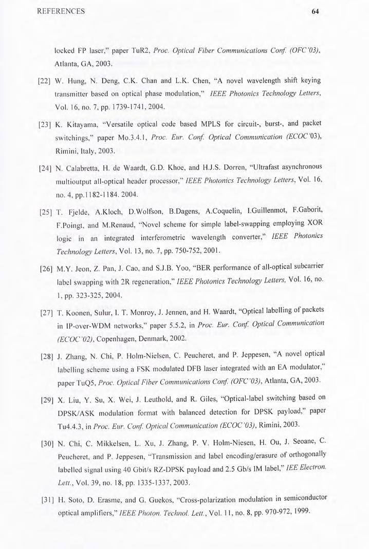
REFERENCES 64
locked FP laser," paper TiiR2, Proc. Optical Fiber Communications Conf. (OFC'03),
Atlanta, G A , 2003.
[22] W . Hung, N . Deng, C.K. Chan and L.K. Chen, "A novel wavelength shift keying
transmitter based on optical phase modulation," IEEE Photonics Technology Letters,
Vol.丨 6, no. 7, pp. 1739-1741,2004.
[23] K . Kitayama, "Versatile optical code based M P L S for circuit-, burst-, and packet
switchings," paper Mo.3.4.1, Proc. Eur. Conf. Optical Communication (ECOC'03),
Rimini, Italy, 2003.
[24] N . Calabretta, H. de Waardt, G.D. Khoe, and H.J.S. Dorren, "Ultrafast asynchronous
multioutpiit all-optical header processor," IEEE Photonics Technology Letters, Vol. 16,
no. 4, pp.1182-1184. 2004.
[25] T. Fjelde, A.Kloch, D.Wolfson, B.Dagens, A.Coquelin, I.Guillenmot, F.Gaborit,
F.Poingl, and M.Renaiid, "Novel scheme for simple label-swapping employing X O R
logic in an integrated interferometric wavelength converter," IEEE Photonics
Technology Letters, Vol. 13, no. 7, pp. 750-752, 2001.
[26] M . Y . Jeon, Z. Pan, J. Cao, and S.J.B. Yoo, “BER performance of all-optical subcarrier
label swapping with 2 R regeneration," IEEE Photonics Technology Letters, Vol. 16, no.
1, pp. 3 2 3 - 3 2 5 , 2 0 0 4 .
[27] T. Koonen, Siiliir, I. T. Monroy, J. Jeniien, and H. Waardt, "Optical labelling of packets
ill IP-over-WDM networks," paper 5.5.2, in Proc. Eur. Conf. Optical Communication
(ECOC '02), Copenhagen, Denmark, 2002.
[28] J. Zhang, N . Chi, P. Holm-Nielsen, C. Peucheret, and P. Jeppesen, “A novel optical
labelling scheme using a F S K modulated D F B laser integrated with an E A modulator,”
paper 'l uQ5, Proc. Optical Fiber Communicaliom Conf. (OFC'03), Atlanta, G A , 2003.
[29] X . Liu, Y . Sii, X . Wei, J. Leuthold, and R. Giles, "Optical-label switching based on
D P S K / A S K modulation format with balanced detection for D P S K payload," paper
TLI4.4.3, ill Proc. Eur. Conf. Optical Commimicadon (ECOC'03), Rimini, 2003.
[30] N . Chi, C. Mikkelsen, L. Xu, J. Zhang, P. V . Holm-Niesen, H. On, J. Seoane, C.
Peiicherel, and P. Jeppesen, ‘‘Transmission and label encoding/erasure of orthogonally
labelled signal using 40 Gbit/s R Z - D P S K payload and 2.5 Gb/s IM label," lEE Electron.
Leti., Vol. 39, no. 18, pp. 1335-1337,2003.
[31] H. Soto, D. Erasme, and G . Guekos, "Cross-polarization modulation in semiconductor
optical amplifiers,"/£££P/7r;/f;/7, Technol. Let(.,Wo\. 11, no. 8, pp. 970-972, 1999.
REFERENCES 65
[32] W . Cai, Y . Dong, M . Zou, Q . Zhang, M . Chen, and S. Xie, "Reduction of waveform
distortion in a semiconductor optical amplifier using internal birefringence and slope
filtering," paper We.P.13, in Proc. Eur. Conf. Optical Communication (ECOC'Ol),
Amsterdam, Netherlands, 2001.
[33] G . P. Agrawal and N . A. Olsson, "Self-phase modulation and spectral broadening of
optical pulses in semiconductor laser amplifiers,” IEEE J. Quantum. Electron., Vol. 25,
no. 11, pp. 2297-2306, 1989.
[34] D. J. Blumenlhal, B. E. Olsson, G . Rossi, T. E. Dimmick, L. Ran, M . Masanovic, 0.
Lavrova, R. Doshi, O . Jerphagnon, J. E. Bowers, V . K a m a n , L. A . Coldren and J.
Barton, "All-optical label swapping networks and technologies," OSA/IEEE J.
Lightwave. TechnoL, Vol. 18, no. 12’ pp. 2058-2075, 2000.
[35J T. K. Chiang; S. K. Agrawal, D. T. Mayweather, D. Sadot, C. F. Barry, M . Hickey, and
L. G . Kazovsky, "Implemenlation of S T A R N E T : a W D M computer communications
network," IEEE Journal on Selected Areas in Commimicalions, Vol 14,no. 5, pp. 824-
839, 1996.
[36J X . Liu, Y . Su, X . Wei, J. Leuthold, and R. Giles, "Optical-label switching based on
D P S K / A S K modulation format with balanced detection for D P S K payload," paper
Tu4.4.3, in Proc. Eur. Conf. Optical Communication (ECOCW), Rimini, Italy, 2003.
|37] N . Chi, C. Mikkelsen, L. Xu, J. Zhang, P. V . Holm-Niesen, H. Ou, J. Seoane, C.
Peucheret, and P. Jeppesen, "Transmission and label encoding/erasure of orthogonally
labelled signal using 40 Gbil/s R Z - D P S K payload and 2.5 Gb/s IM label," lEE Electron.
乙 e"., Vol.39, no. 18,pp. 1335-1337, 2003.
[38] N . Deng, Y . Yang, C.K. Chan, W . Hung, and L.K. Chen, "Intensity-modulated labeling
and all-optical label swapping on angle-modulated optical packets," IEEE Photon.
Technol. Lett.. Vol. 16, no. 4, pp. 1218-1220, 2004.
[39] G , P. Agrawal, Fiber-optic conummication systems, 3rd Ed, Wiley-lnterscience, pp. 176-
177,2002.


SiflhhThDD