Exploiting Processor Heterogeneity Through Reconfigurable ...

Journal of VLSI Signal Processing 28, 63–83, 2001c© 2001 Kluwer Academic Publishers. Manufactured in The Netherlands.
Application of Reconfigurable Computing to a High PerformanceFront-End Radar Signal Processor∗
DAVID R. MARTINEZ, TYLER J. MOELLER AND KEN TEITELBAUMMIT Lincoln Laboratory, 244 Wood Street, Lexington, MA 02420-9108
Received July 1999; Revised December 1999
Abstract. Many radar sensor systems demand high performance front-end signal processing. The high processingthroughput is driven by the fast analog-to-digital conversion sampling rate, the large number of sensor channels,and stringent requirements on the filter design leading to a large number of filter taps. The computational demandsrange from tens to hundreds of billion operations per second (GOPS). Fortunately, this processing is very regular,highly parallel, and well suited to VLSI hardware. We recently fielded a system consisting of 100 GOPS designedusing custom VLSI chips. The system can adapt to different filter coefficients as a function of changes in thetransmitted radar pulse. Although the computation is performed on custom VLSI chips, there are important reasonsto attempt to solve this problem using adaptive computing devices. As feature size shrinks and field programmablegate arrays become more capable, the same filtering operation will be feasible using reconfigurable electronics. Inthis paper we describe the hardware architecture of this high performance radar signal processor, technology trendsin reconfigurable computing, and present an alternate implementation using emerging reconfigurable technologies.We investigate the suitability of a Xilinx Virtex chip (XCV1000) to this application. Results of simulating andimplementing the application on the Xilinx chip is also discussed.
Keywords: VLSI rader signal processor, front end high performance filtering, reconfigurable hardware, digitalfiltering mapped to reconfigurable computing, commercial FPGA hardware
1. Introduction
The radar signal processing trend is to bring the analog-to-digital converter (ADC) closer to the radar antennaelements, and process the incoming signals digitallyinstead of using more conventional analog approaches.The digital hardware offers more robust system stabil-ity, avoiding unnecessary calibrations characteristic ofanalog hardware due to component drifts with time andtemperature. The availability of digital hardware alsoprovides very important benefits, such as, more flex-ibility in waveform design, an ability to reconfigure
∗This work was sponsored by the Air Force under contract F19628-95-C-0002. Opinions, interpretations, conclusions, and recommen-dations are those of the authors and are not necessarily endorsed bythe United States Air Force.
the hardware by downloading different system coeffi-cients, and an easier upgrade path as digital electronicscontinues to advance at an exponential rate commen-surate with Moore’s law.
The benefits of digital hardware, in advanced radarsignal processing systems, come at the expense of verypotent front-end signal processors needs. The com-putational and data throughputs result from the largeamount of incoming data processed over a very shorttime interval. The computational throughputs are inthe tens to hundreds of billion operations per second(GOPS). The data throughput bandwidths are in thehundreds of megabytes per second (MBytes/sec). Inaddition to stringent computational and data through-puts, the digital hardware must be deployed in a smallsize, low weight, and low power. Furthermore, the hard-ware must also comply with demanding environmental,
64 Martinez, Moeller and Teitelbaum
shock, vibration, humidity, and temperature specifi-cations. Examples of platforms requiring these capa-bilities are today’s airborne early warning radars, un-manned air vehicles (UAVs), fighters, and spacebornesurveillance and targeting radars.
For the past several years, commercially availabledigital signal processors (DSPs) or RISC microproces-sors have not met the system requirements for caseswhere we need in excess of 10 GOPS/ft3 and≥0.5GOPS/Watt, operating on at least 16-bit data. Fortu-nately, the front-end signal processing functions arevery regular, well structured, and often times indepen-dent of the incoming data. Therefore, most implemen-tations to date have used either commercially available,yet dedicated, compute engines (e.g., INMOS A100 orSHARP LH9124 FFT chip), or custom VLSI designs.These approaches have allowed us to meet the compu-tational throughputs and data throughputs, within theform factor and environmental requirements.
In this paper, we describe a recently fielded front-end signal processor capable of 100 GOPS. Since thissystem is channel parallel, it can be scaled to manyhundreds of GOPS as we increase the number of radarinput channels. The system can also be reconfigured ina few milliseconds for a different set of coefficients. Al-though the system requirements led us to choose a cus-tom VLSI implementation, we believe that this applica-tion is very well matched to reconfigurable computinghardware. At the time when the custom VLSI designstarted (circa 1996–1997), the commercially availablefield programmable gate arrays were not able to meetthe system requirement by a large margin. However,the rapid growth in computational capability of morerecent reconfigurable devices provides a new opportu-nity for meeting the requirements without dependingon point solutions.
Reconfigurable computing will offer many of thesame benefits provided by commercial general purposemicroprocessors without sacrificing overall system per-formance. These devices will be cost effective, sincethe same hardware can be reused for many differentapplications. The economies of scale will result in avery cost-effective solution. Furthermore, for a givendesign, the implementation cycle is shorter than cus-tom VLSI solutions. If the first design contains flaws,one can redo the hardware configuration in software.These changes would be very costly with custom VLSI.Finally, because of the large number of devices, recon-figurable hardware manufactures can rip the benefits ofthe latest reductions in lithography feature size.
We are not implying that all front-end radar signalprocessing can be solved using reconfigurable comput-ing. There are still system specifications, for example,in spaceborne applications, where custom VLSI solu-tions are further ahead than reconfigurable hardware,particularly when we need solutions with throughputsper unit power≥20 GOPS/W, data throughputs exceed-ing GBytes/sec, and compliant with radiation harden-ing requirements.
The example presented in this paper represents anadvanced prototype that only a few years back wouldhave been unacceptable to attempt to solve using fieldprogrammable gate arrays. This example serves as ameasure of how far reconfigurable technologies havecome in just three years. As discussed in Section 4,under technology trends, this rapid advance can becredited to several factors, such as, smaller lithographysize, advancements in development tools, lower volt-ages, and algorithms that exploit the distributed mem-ory architecture of field-programmable gate arrays(FPGAs).
The paper is divided as follows. In the next section,we describe the front-end radar digital filtering and theassociated computational requirements. In Section 3,the custom VLSI approach is presented. Section 4 ad-dresses the technology trends and drivers fueling theadvances experienced with reconfigurable electronicscompared to more general purpose computing. InSection 5, we review and contrast several architectureapproaches to solve the front-end radar signal process-ing posed in Section 2. In Section 6, we discuss otherfuture candidate applications for reconfigurable com-puting technologies. Finally, in Section 7 we presentour conclusions and summary.
2. Front-End Digital Filtering
A typical radar signal processing flow starts at the out-put of the ADC with real-time data processed througha set of digital filters. The digital filters are needed tofirst convert the data from real ADC samples to com-plex digital in-phase and quadrature (DIQ) samples.This operation is commonly known in the radar com-munity as DIQ sampling [1]. The DIQ sampling is nec-essary to preserve the target Doppler information. Fromthe Doppler information one can discern the targetvelocity.
As illustrated in Fig. 1, the digital filtering is typicallythe first step in the signal processing chain. The remain-ing processing, Doppler filtering, adaptive nulling, and

Application of Reconfigurable Computing 65
Figure 1. Typical radar signal processing flow.
post-nulling processing, can also be very demanding.However, in this paper we only focus in on DIQ sam-pling. J. Ward [2] presents a thorough exposition ofthe typical radar signal processing flow, with particu-lar emphasis on space-time adaptive processing. DIQsampling is proportional in computational operationsto the data bandwidth of the system, the number of filtertaps, and the number of channels, as shown in Fig. 1.In the next subsection we describe in more detail thefilter specifications.
2.1. DIQ Sampling Architecture
The radar data after the ADC will exhibit a set of spec-trum replicates with periodicity equal to the Nyquistsampling (1/2 the sampling rate). Because the data arereal samples, at this stage the spectrum maintains equalimages with respect to 0 Hz. The DIQ filtering willserve the purpose of extracting one of the sidebands,mapping the sideband spectrum to baseband, and fil-tering all remaining images including any DC offsetsintroduced by the ADC. The filter coefficients willvary depending on the characteristics of the bandwidthpresent in the transmitted radar pulse. The resultingoutput contains a single sideband spectrum replicatedevery increment of the sampling frequency. The sin-gle sideband represents the complex signal (in-phaseand quadrature components) characteristic of a Hilberttransform performed in a demodulation operation [3].
The analog receiver filtering, prior to the ADC con-verter, is selected such that the information bandwidthis preserved without aliasing. The signal instantaneousbandwidth is typically several factors below the ADCsampling frequency. This oversampling leads to verysimple DIQ architectures.
For example, if the ADC sampling is four times theinstantaneous frequency of the radar [4], the mappingof the spectrum to baseband reduces to multiplicationby +1, 0, and−1 for the in-phase component, and 0,+1, and−1 for the quadrature component. Once thedata are mapped to baseband, the complex signal can befiltered and decimated to match the signal bandwidth.This simplification leads to the typical DIQ samplingarchitecture shown in Fig. 2. We use two filter banksof equal length, each operating on the in-phase andquadrature samples, respectively. The odd samples areused to form the in-phase component, and the evensamples are used to form the quadrature components.
Figure 2. Digital in-phase and quadrature sampling architecture.
66 Martinez, Moeller and Teitelbaum
2.2. Digital Filter Specifications
The DIQ filter is designed to suppress all out of bandimages and spurious signals, including any DC offsetfrom the ADC. The filter must maintain a minimumripple across the passband with a sidelobe level suffi-ciently down to attenuate any unwanted data outside thesignal bandwidth. The filter skirts determine the num-ber of taps in the filter. For our application, we usedthe Parks-McClellan Remez algorithm [3] available inMatlab to design a finite impulse response filter withlinear phase. The characteristics of the filter were asfollows [5]:
• Equiripple passband= 0.18 dB• Stopband level≥ 80 dB• Unattenuated passband= 0.25 MHz• Bandwidth at 3 dB points= 0.381 MHz
The above specifications led to a filter with 208 com-plex taps (104 taps for the real and 104 taps for theimaginary components, respectively). In order to meetthe filter stopband level the coefficients must have afinite precision of at least 15 bits.
The ADC used was a DATEL ADS945 sampling at10 MHz, with a precision of 14 bits. After the digital fil-ter, shown in Fig. 2, the radar data were decimated by afactor of 16 or, equivalently, a factor of 8 complex sam-ples. Thus, the output sampling rate out of the DIQ filterwas down to 0.625 MHz complex data. Although thisoutput data rate was twice what was needed to main-tain the signal information bandwidth, it simplified thefollowing filtering stage past the DIQ sampling result-ing in a simpler filter design with a smaller number oftaps.
On a per channel basis, as shown in Fig. 1, the com-putational throughput is proportional to the data band-width and the number of filter taps. For the 208 com-plex filter taps and an input data rate of 10 MHz, theDIQ filter must perform at least 2.08 GOPS, basedon the architecture shown in Fig. 2. The reductionin sampling rate by a factor of 8 could have allowedus to only process the samples needed at the out-put. However, the hardware designer [6] concludedthat the custom VLSI implementation was more reg-ular and easier to layout by processing all the in-coming samples and decimating at the end. For a 48-channel system the total computation throughput was100 GOPS.
3. Custom VLSI Implementation
The front-end signal processor design begun in 1996.The system was completed in 1998. At the start of theproject, a detailed search was done to determine if ei-ther general purpose hardware or commercially avail-able dedicated chips could be used to solve the DIQsampling requirements. We concluded that no DSP orRISC chips would be suitable to meet the processingrequirements, particularly when you account for theloss in processing efficiencies caused by programmablehardware. There were several commercially special-ized chips designed specifically to perform FIR filter-ing (e.g., Gray chip GC2011, Harris HSP43168, GECPlessey PDSP16256). We concluded that none of thesechips met the requirements in all the critical dimen-sions, such as, input data precision bits, coefficient pre-cision bits, internal arithmetic accuracy, and computa-tion throughput at low power.
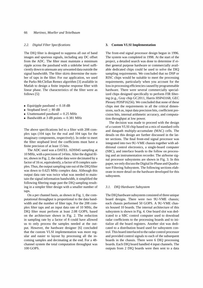
The decision was made to proceed with the designof a custom VLSI chip based on a mix of standard cellsand datapath multiply-accumulate (MAC) cells. Thedetails on this design are further discussed in the lat-ter sections. The final front-end signal processor wasintegrated into two 9U-VME chassis together with ad-ditional control electronics, a single-board computer(SBC), and interface boards to the follow on process-ing and an instrumentation recorder. The airborne sig-nal processor subsystems are shown in Fig. 3. In thispaper, we only discuss the Digital In-Phase and Quadra-ture Filtering Subsystem. The following sections elab-orate in more detail on the hardware developed for thissubsystem.
3.1. DIQ Hardware Subsystem
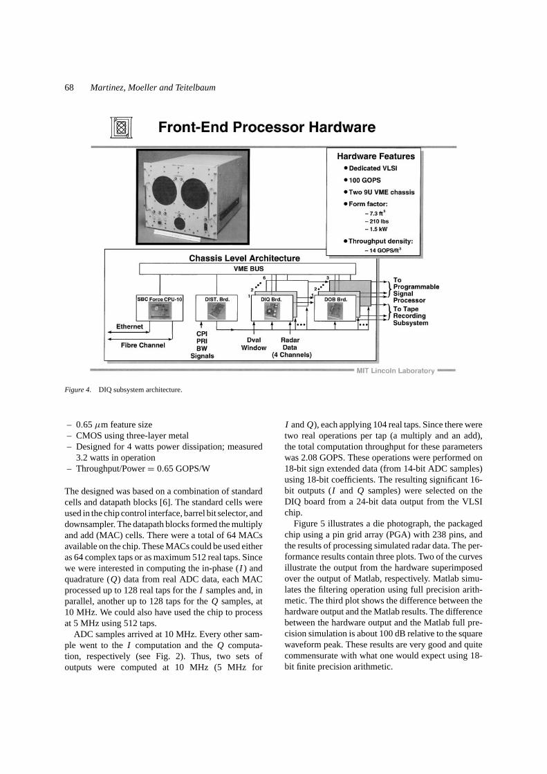
The DIQ hardware subsystem consisted of three uniqueboard designs. There were two 9U-VME chassis;each chassis performed 50 GOPS. A 9U-VME chas-sis housed 10 boards. The internal architecture of thissubsystem is shown in Fig. 4. One board slot was ded-icated to a SBC control computer used to downloadradar coefficients to the processing boards and to ini-tialize all the board registers. Another slot was dedi-cated to a distribution board used for subsystem con-trol. This board interfaced to the radar control processorand provided control signals to each of the subsequentboards in the chassis. There were 6 DIQ processingboards. Each DIQ board handled 4 input channels. Theoutputs from 2 DIQ boards were then sent to a data
Application of Reconfigurable Computing 67
Figure 3. Airborne signal processor subsystems.
output board (DOB board). Each DOB board packedthe data and provided the same interface outputs toa back-end programmable processor and to an instru-mentation recorder. These custom boards were basedon a 14-layer PCB design of size 9U× 220 mm.The overall characteristics of this subsystem for two9U-VME chassis were:
• 100 GOPS• Size= 7.3 ft3
• Weight= 210 lbs• Power= 1.5 KW• Chassis throughput/Power= 67 MOPS/W• Throughput density= 14 GOPS/ft3
• Power density= 205 W/ft3
There were 24 channels input to each DIQ subsys-tem chassis. The total data rate to the chassis was420 MBytes/sec. These data were then distributed to6 DIQ processing boards over a custom backplane.Each DIQ board received 70 MBytes/sec of data. Therewere 4 custom VLSI chips per DIQ board; each chip
processed one channel of data. The input data wasmapped to 18-bit data on the DIQ board prior to go-ing into the VLSI chip. The output of the chip wasa 24-bit data word. A 16-bit word was then selectedand sent over the custom backplane to the DOB board.Thus, the output of the DIQ board was reduced down to10 MBytes/sec (4 channels, 16-bit complex words, at0.625 MHz). The next section describes in more detailthe custom VLSI hardware.
3.2. Custom VLSI Hardware
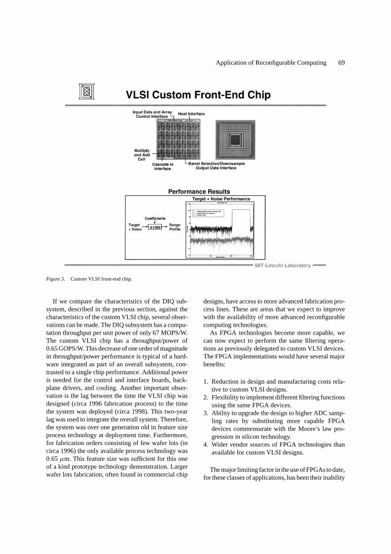
The VLSI custom front-end chip, designed using 1996process technology, is shown in Fig. 5. The chip wasfabricated at the National Semiconductor facility in Ar-lington, Texas, under the C050 process. The key fea-tures of this chip were:
– 2.08 billion operations per second– 18-bit input data and coefficients; 24-bit output data– 585 mil× 585 mil die size– 1.5 million transistors
68 Martinez, Moeller and Teitelbaum
Figure 4. DIQ subsystem architecture.
– 0.65µm feature size– CMOS using three-layer metal– Designed for 4 watts power dissipation; measured
3.2 watts in operation– Throughput/Power= 0.65 GOPS/W
The designed was based on a combination of standardcells and datapath blocks [6]. The standard cells wereused in the chip control interface, barrel bit selector, anddownsampler. The datapath blocks formed the multiplyand add (MAC) cells. There were a total of 64 MACsavailable on the chip. These MACs could be used eitheras 64 complex taps or as maximum 512 real taps. Sincewe were interested in computing the in-phase (I ) andquadrature (Q) data from real ADC data, each MACprocessed up to 128 real taps for theI samples and, inparallel, another up to 128 taps for theQ samples, at10 MHz. We could also have used the chip to processat 5 MHz using 512 taps.
ADC samples arrived at 10 MHz. Every other sam-ple went to theI computation and theQ computa-tion, respectively (see Fig. 2). Thus, two sets ofoutputs were computed at 10 MHz (5 MHz for
I andQ), each applying 104 real taps. Since there weretwo real operations per tap (a multiply and an add),the total computation throughput for these parameterswas 2.08 GOPS. These operations were performed on18-bit sign extended data (from 14-bit ADC samples)using 18-bit coefficients. The resulting significant 16-bit outputs (I and Q samples) were selected on theDIQ board from a 24-bit data output from the VLSIchip.
Figure 5 illustrates a die photograph, the packagedchip using a pin grid array (PGA) with 238 pins, andthe results of processing simulated radar data. The per-formance results contain three plots. Two of the curvesillustrate the output from the hardware superimposedover the output of Matlab, respectively. Matlab simu-lates the filtering operation using full precision arith-metic. The third plot shows the difference between thehardware output and the Matlab results. The differencebetween the hardware output and the Matlab full pre-cision simulation is about 100 dB relative to the squarewaveform peak. These results are very good and quitecommensurate with what one would expect using 18-bit finite precision arithmetic.
Application of Reconfigurable Computing 69
Figure 5. Custom VLSI front-end chip.
If we compare the characteristics of the DIQ sub-system, described in the previous section, against thecharacteristics of the custom VLSI chip, several obser-vations can be made. The DIQ subsystem has a compu-tation throughput per unit power of only 67 MOPS/W.The custom VLSI chip has a throughput/power of0.65 GOPS/W. This decrease of one order of magnitudein throughput/power performance is typical of a hard-ware integrated as part of an overall subsystem, con-trasted to a single chip performance. Additional poweris needed for the control and interface boards, back-plane drivers, and cooling. Another important obser-vation is the lag between the time the VLSI chip wasdesigned (circa 1996 fabrication process) to the timethe system was deployed (circa 1998). This two-yearlag was used to integrate the overall system. Therefore,the system was over one generation old in feature sizeprocess technology at deployment time. Furthermore,for fabrication orders consisting of few wafer lots (incirca 1996) the only available process technology was0.65µm. This feature size was sufficient for this oneof a kind prototype technology demonstration. Largerwafer lots fabrication, often found in commercial chip
designs, have access to more advanced fabrication pro-cess lines. These are areas that we expect to improvewith the availability of more advanced reconfigurablecomputing technologies.
As FPGA technologies become more capable, wecan now expect to perform the same filtering opera-tions as previously delegated to custom VLSI devices.The FPGA implementations would have several majorbenefits:
1. Reduction in design and manufacturing costs rela-tive to custom VLSI designs.
2. Flexibility to implement different filtering functionsusing the same FPGA devices.
3. Ability to upgrade the design to higher ADC samp-ling rates by substituting more capable FPGAdevices commensurate with the Moore’s law pro-gression in silicon technology.
4. Wider vendor sources of FPGA technologies thanavailable for custom VLSI designs.
The major limiting factor in the use of FPGAs to date,for these classes of applications, has been their inability

70 Martinez, Moeller and Teitelbaum
to reach computation throughputs on the order of sev-eral GOPS, with 18-bit data and coefficient inputs, anda throughput per unit power greater than 0.5 GOPS/W.Most FPGA demonstrations to date have been limitedto a few bits of precision. The custom VLSI implemen-tation, described in this section, serves as an existingproof and benchmark of capabilities we would like tosee in FPGAs. In the following sections we discussthe recent observed FPGA technology trends. We alsopresent implementation techniques and results showingwhat is feasible to date with the most advanced FPGAdevices. We show how close this hardware comes tomeeting our FIR filtering requirements.
4. Technology Trends in Field ProgrammableGate Arrays
The increasing sophistication of radar signal process-ing techniques has paralleled improvements in digitalcomputing techniques. Computational requirements offuture radar systems will approach 10 TOPS (trillionoperations per second) during the next decade, plac-ing it in the domain occupied by the leading edge ofcommercial massively parallel processors consisting ofhundreds or thousands of individual CPUs. Unfortu-nately, the sheer bulk of these systems will precludetheir use in most military radar applications whereplatform constraints place stringent requirements onsize, weight and power. Reconfigurable computinghas the potential to mitigate this problem by offload-ing computationally intensive tasks for execution ontoFPGAs.
Compared to the digital computer industry, FPGAsare in their infancy. Xilinx, the leading manufacturer ofFPGAs produced its first field programmable gate ar-ray 15 years ago [7]. The initial devices were primitiveby today’s standards, and FPGAs were mainly used for“glue logic.” The programmable nature of the devicemade it possible for engineers to make circuit designchanges without costly and time-consuming modifica-tions to printed circuit boards, and the fledgling indus-try prospered. As technology progressed and the pro-cess geometry shrank, both the capacity and speed ofFPGAs have increased. These improvements have en-abled FPGAs to perform the arithmetic functions nec-essary for digital signal processing (DSP). The goalof reconfigurable computing is to design application-independent hardware based on FPGA technology,and download application-specific algorithms to han-dle a wide variety of potential applications. Several
manufacturers currently offer such products withmany FPGAs, external memory, and industry-standardinterfaces.
4.1. Building Blocks
In simplest terms, FPGAs are nothing more than largearrays of look-up tables (LUTs) with a flexible inter-connect which allows building complex circuits withmultiple LUTs. Once the circuit is described (eitherwith VHDL or with schematic capture), the chore ofmapping of these circuits onto the sea of LUTs is ac-complished with automated tools for synthesis, place-ment, and routing.
For the Xilinx devices, the basic building block iscalled a Configurable Logic Block (CLB) that consistsof two 4-input LUTs, one 3-input LUT, and two reg-isters. DSP functions consist principally of multiplyand add operations that must be constructed of mul-tiple CLBs. A b-bit adder needsb LUTs andb regis-ters, and thus consumesb/2 CLBs. A b× b bit mul-tiplier requires 2b b-bit adders consumingb2 CLBs.A FIR filter tap (multiply-add, 2 real operations) con-sumes (b2+ b/2) CLBs. For 16-bit arithmetic, an adderwould consume only 8 CLBs, but a multiplier wouldtake 264 CLBs.
In order to promote a more industry-standard ap-proach to counting FPGA capacities, Xilinx has pro-posed the notion of a Logic Cell [8] which consistsof a 4-input LUT and a register. For comparison pur-poses, the Xilinx XC4000 family CLB is equivalent to2.375 logic cells.
Since the parallel multiplier has been so expensivein terms of resources used (CLBs) compared to re-sources available on a single FPGA, several alterna-tive strategies for implementing DSP functions haveevolved. These strategies tend to exploit the LUT-basedarchitecture of the FPGA.
When multiplying a data stream by a constant thatis known a priori, a constant coefficient multiplier [9]may be used to look up the product of the data sampleand coefficient. The data sample effectively becomesthe address to the look-up table that stores the prod-uct of the coefficient and data sample for each possi-ble value of the data sample. Also assuming a prioriknowledge of multiplier constants, Serial DistributedArithmetic (SDA) [10] rearranges the order of com-putations to facilitate table lookup of a 1-bit sum ofproducts. Distributed arithmetic has also been used toimplement Fast-Fourier Transforms (FFTs) [11].

Application of Reconfigurable Computing 71
These techniques work well for many digital-filtering applications where the filter coefficients (im-pulse response) are fixed. For adaptive filters wherethe coefficients are changed in response to the data,other approaches are necessary. It is possible to buildSDA filters with two banks of filter taps that are bankswapped when filter coefficients are updated [12]. Inthe latter sections under implementation, this is the ap-proach used for handling multiple filter coefficients inreal-time. A table generator computes the LUT con-tents in real time while the new filter coefficients aredownloaded. While this is obviously less resource effi-cient than the straightforward SDA approach, it is stillan improvement over having to use parallel multipliers.
4.2. Benchmarks
In assessing the computational requirements of DSPalgorithms, and the capabilities of DSP technologies,the metric commonly used is the number of arithmeticoperations to be executed per unit time. This is typicallyexpressed in MOPS (million operations per second) orGOPS (billion operations per second). For consideringthe performance of FPGAs, this metric is normalizedby the “area” consumed by the circuit (the number ofCLBs) to yield MOPS/CLB. If the multiply-adder canoperate at a clock rate offC, then the number of oper-ations per second executed per CLB is:
2* fC/(b2+ b/2) (1)
FPGAs are much more effective for small word lengthssince computation rate per unit area (MOPS/CLB) fallsoff as the square of the word length in bits. This isclearly evident in the graph in Fig. 6, which is basedon the Xilinx CORE benchmarks [13].
Figure 6 also illustrates the performance advantageachievable with SDA compared to parallel multiply-add architectures. The product of the MOPS/CLB met-ric and the device capacity (number of CLBs) give anotion of the device capability in aggregate. For exam-ple, if Xilinx’s new Virtex device (XCV1000) whichhas 12,288 CLBs (equivalent CLBs with respect to Xil-inx 4000 series) could achieve 1 MOPS/CLB, it wouldbe able to perform about 12 GOPS per chip.
In many DSP applications, power consumption isheavily constrained. For these applications, MOPS/Watt is a convenient performance metric. Xilinx [14]has suggested a simple formula for estimating the
Figure 6. Xilinx core benchmarks.
power consumption of a device:
P = Vcc∗Kp
∗ fC∗NLC
∗ TogLC (2)
WhereVcc is the supply voltage,Kp is a device-specificpower factor,fC is the maximum clock frequency,NLC
is the number of logic cells and TogLC is the frac-tion of logic cells toggling on each clock (typicallyabout 20%). Rearranging (1) and (2), and assuming2.375 logic cells per CLB yields the following estimatefor MOPS/Watt:
MOPS/Watt= 4.2e−6/[Vcc∗Kp
∗ (b2+ b/2)] (3)
Typical values for several generations of Xilinx partsare shown in Table 1 and assume 16-bit arithmetic.Power efficiencies for several 32-bit floating point pro-grammable processors are shown in Table 2 for com-parison.
Table 1. Power efficiency (MOPS/W) for severalFPGA families.
Part number Vcc Kp × 1012 MOPS/W
XC4000E 5 72 43.0
XC4000EX 5 47 65.9
XC4000XL 3.3 28 167.5
XC4000XV 2.5 13 476.3
XCV (Virtex) 2.5 6.8 961.2
72 Martinez, Moeller and Teitelbaum
Table 2. Power efficiency (MFLOPS/W) for several floating-point programmable microprocessors.
Processor Peak MFLOPS Power (W) (Typical) MFLOPS/W
DEC Alpha 21164 1200 46 26
INTEL Pentium III 1000 28 35.7
Motorola Power PC 750 800 8 138
Analog Devices 21062 (SHARC) 120 2 60
Analog Devices 21160 600 2 300
Texas Instruments TMS320C6701 1000 2.8 357
4.3. Technology Trends
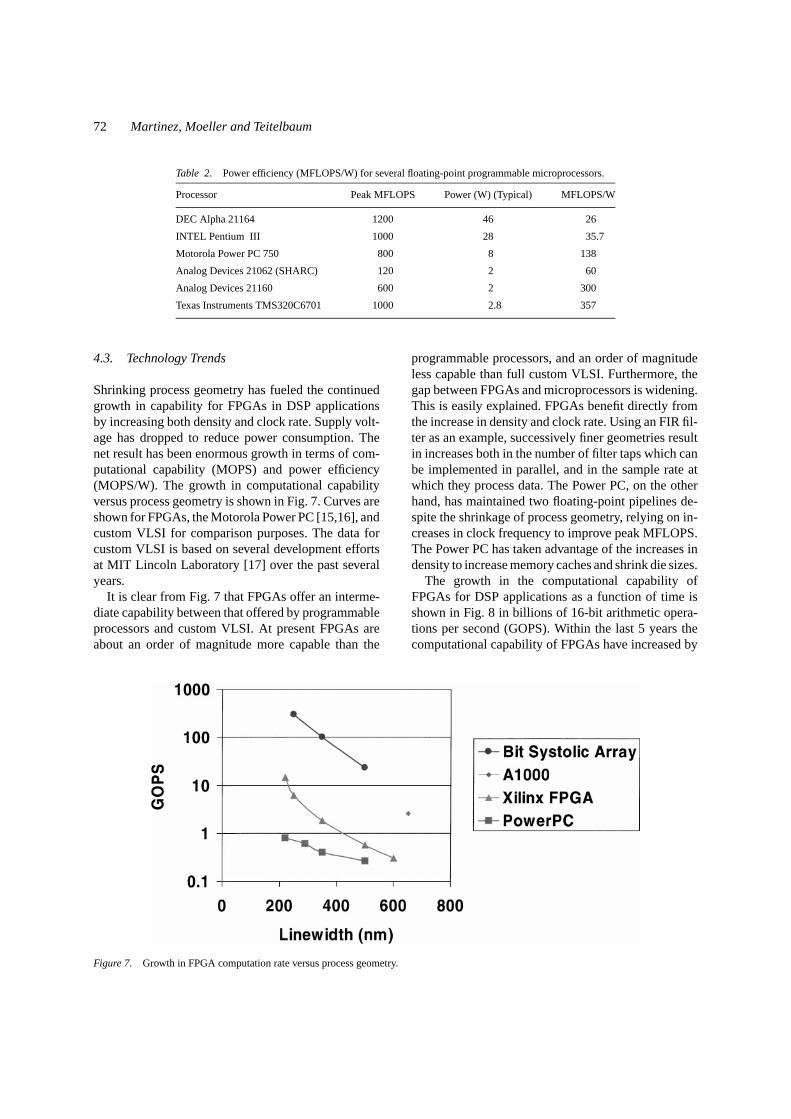
Shrinking process geometry has fueled the continuedgrowth in capability for FPGAs in DSP applicationsby increasing both density and clock rate. Supply volt-age has dropped to reduce power consumption. Thenet result has been enormous growth in terms of com-putational capability (MOPS) and power efficiency(MOPS/W). The growth in computational capabilityversus process geometry is shown in Fig. 7. Curves areshown for FPGAs, the Motorola Power PC [15,16], andcustom VLSI for comparison purposes. The data forcustom VLSI is based on several development effortsat MIT Lincoln Laboratory [17] over the past severalyears.
It is clear from Fig. 7 that FPGAs offer an interme-diate capability between that offered by programmableprocessors and custom VLSI. At present FPGAs areabout an order of magnitude more capable than the
Figure 7. Growth in FPGA computation rate versus process geometry.
programmable processors, and an order of magnitudeless capable than full custom VLSI. Furthermore, thegap between FPGAs and microprocessors is widening.This is easily explained. FPGAs benefit directly fromthe increase in density and clock rate. Using an FIR fil-ter as an example, successively finer geometries resultin increases both in the number of filter taps which canbe implemented in parallel, and in the sample rate atwhich they process data. The Power PC, on the otherhand, has maintained two floating-point pipelines de-spite the shrinkage of process geometry, relying on in-creases in clock frequency to improve peak MFLOPS.The Power PC has taken advantage of the increases indensity to increase memory caches and shrink die sizes.
The growth in the computational capability ofFPGAs for DSP applications as a function of time isshown in Fig. 8 in billions of 16-bit arithmetic opera-tions per second (GOPS). Within the last 5 years thecomputational capability of FPGAs have increased by

Application of Reconfigurable Computing 73
Figure 8. Growth of computational capability for Xilinx FPGAs(16-bit arithmetic operations).
an order of magnitude every two years, and we havereached the point where it is now feasible to explorethe implementation of complex DSP systems using FP-GAs as the computational building blocks. In the nextsections we present implementation approaches for theFIR digital filtering function shown in Fig. 1 using theXilinx Virtex XCV1000 as an example of state-of-the-art FPGAs.
5. Reconfigurable Hardware for FIRDigital Filtering
To demonstrate the current state of FPGA technologyand its application to front-end signal processing, anFPGA design meeting the design requirements of MITLincoln Laboratory’s custom VLSI FIR chip was cre-ated [19]. Although the actual VLSI chip was capable ofprocessing, in the DIQ mode, 256 taps (I andQ com-ponents) for input data at 10 MHz, the design couldaccommodate up to 512-tap real filter with 5 MHz in-put data. Therefore, the FPGA demonstration was pre-sented with the requirement to also accommodate up to512 taps at a maximum input data rate of 5 MHz. Thisrequirement is equivalent to 10 MHz input data with amaximum of 256 taps. The FPGA requirements were:
• Perform 512-tap real FIR filtering.• Accept a minimum of 16-bit data at a maximum input
rate of 5 MHz.
• Operate with a maximum chip clock frequency of40 MHz (eight times the input data rate).• Output data with the same precision as the custom
VLSI chip (the VLSI chip outputs 24-bits of data,but simulations showed 18-bits of accurate precisionwas sufficient).• Use two swappable banks of 18-bit coefficients, one
active and one loadable.• Fit into the largest Xilinx FPGA available, the Virtex
XCV1000.• Coefficient banks must be able to be switched every
1 ms (i.e. reloading all 512 coefficients must takeplace in less than 1 ms), and the new bank of coeffi-cients must become active instantaneously.
The 16-bit inputs were chosen for the FPGA imple-mentation as the custom VLSI chip is currently beingused with an ADC with a 14-bit output, and it is un-likely the VLSI chip would operate with an ADC ofmore than 16-bits in the future. The only reason forhaving the custom VLSI chip designed to accommo-date 18-bit input data was to facilitate word growth ifseveral custom A1000 chips were used in a cascadedmode. This is not a requirement imposed on the FPGAimplementation, because for the DIQ filtering functionthere was no need to cascade multiple chips.
Two banks of coefficients were used in the customVLSI chip. This capability is also required for theFPGA; so that one bank stores the active filter coef-ficients while the other bank is being loaded with newcoefficients. The banks may then be swapped by an ex-ternal control so that the new coefficients may becomeinstantly active.
Although the need to change coefficients could beviewed as an ideal application for reconfiguration, us-ing swappable coefficient banks is more efficient. Ithas been proposed that the ability of an FPGA to bereconfigured in-system be used to implement a singlefilter with fixed coefficients that is reconfigured when acoefficient switch is desired. The design requirementsspecify an instantaneous switch between the active co-efficients and the new set of loaded coefficients. How-ever, this prohibits using a single bank of coefficientsthat could be reconfigured via the FPGA’s reconfigu-ration ability. The filter would be inactive during thereconfiguration time, which is unacceptable. This slowreconfiguration is one of the important limitations withtoday’s reconfigurable technologies.
One solution might be to have one filter operationalwhile a second filter was being configured in the same
74 Martinez, Moeller and Teitelbaum
chip. This would require the FPGA to have partial re-configuration ability. In addition, the filter coefficientswould have to be known in advance so that configu-rations using constant coefficients could be mapped,placed, and routed by the Xilinx software to be readyfor loading into the FPGA. These configurations wouldthen have to be stored off-chip to be recalled and loadedinto the FPGA. In most applications, the filter responsesare not known beforehand, so creating and storing ev-ery configuration for every set of possible coefficientsis not feasible.
5.1. Implementation Techniqueson Reconfigurable Hardware
Several different implementation techniques were in-vestigated to find a design with the best performance(or at least satisfying the design requirements) withthe minimum amount of FPGA utilization. These tech-niques included: a parallel MAC structure (much likethat used in the custom A1000 VLSI design), a bit-levelsystolic structure (similar to that used in another MITLincoln Laboratory custom VLSI chip), and a bit-serialapproach using Distributed Arithmetic (DA). The tech-nique that was discovered to have the best performancefor the smallest area was the bit-serial DA approach[19].
In addition to the DA approach, we also investigatedthe fast FIR algorithm (FFA) and filtering in the fre-quency domain. Although these are techniques thatcould be used in a VLSI solution, they would not lendthemselves as easily to a multi-mode chip. The customVLSI A1000 chip was designed to be able to performreal, complex, or DIQ digital filtering with the samehardware. The FPGA configuration does not need tosupport multiple modes. Instead, a specific implemen-tation can be developed for each mode, and the correctFPGA configuration can be loaded into the reconfig-urable hardware for the mode desired.
The next section describes the implementation ofDIQ filtering using the DA approach [18]. Additionally,a custom layout tool is discussed. This tool, developedat MIT Lincoln Laboratory, aids in the automatic place-ment of regular and pipelined FPGA VHDL designs[19]. Currently, there is no way, through the Xilinxdevelopment flow, to describe how synthesized com-ponents from a design written in VHDL should be laidout within a FPGA. A designer may develop a highlypipelined design that requires only short net lengths be-tween logic and pipeline stages. However, by breaking
the design into small, regular, systolic cells, the devel-opment tools have no knowledge of the fact that a singlecell needs to be laid out only once and that cells thatcommunicate with each other should be placed nextto each other. Presently, the tools place every singlesynthesized component individually, resulting in inef-ficient designs with long net lengths that lead to lowclock performance results. The MIT Lincoln Labora-tory custom tool will read, through the VHDL hierar-chy, the user-defined placement constraints embeddedwithin the VHDL for low-level, regular structures. Thetool will also develop an overall placement scheme thatwill keep the same layout for identical repeated systoliccells, and will place connecting cells adjacent to eachother. The DA implementation and the FPGA complex-ity are described in the following section.
5.2. DIQ Filtering Implementation Basedon Distributed Arithmetic
The abundance of small distributed RAM blocksthroughout the Xilinx FPGA chip enables the user topre-calculate partial products, and to load these intothe distributed RAM, thereby eliminating the largeamounts of logic needed to compute multiplicationresults in a non-distributed approach. A DistributedArithmetic (DA) architecture is a versatile approachto using this distributed RAM [10, 20–24].
The 16× 1 RAM units within the Xilinx CLBs aregood candidates for this DA scheme. One bit of a sin-gle 4-input LUT can fit into one of these units withno unused logic. For FIR filters larger than 4-taps,the filter can be broken into four tap groups. For ex-ample, a 16-tap FIR is shown in Fig. 9. To eliminateoverflow, each adder stage must grow by one bit, andthe scaling accumulator must also grow accordinglyin size (of course, the scaling accumulator could dropthe lower bits in its accumulation if less precision isrequired).
The shift registers required by each four-tap groupcan be implemented in the Xilinx Virtex distributed16× 1 RAM for 16-bit (or less) inputs. Each 16×1 RAM block may be configured to act as (up to) a16-bit shift register. The length of the register is spec-ified by the value written into the RAM block’s 4-bitaddress. Each clock cycle a bit is shifted into the frontof the register from the RAM’s data input, and a bitis shifted out of the end of the register to the RAM’sdata output. With this technique, a single CLB can holdthe entire 16-bit input for two taps. This is much more

Application of Reconfigurable Computing 75
Figure 9. 16-Tap serial distributed FIR.
efficient than using registers to form each tap’s shiftregister.
Figure 9 could be expanded until a 512-tap filterhas been constructed, but two problems would exist.First of all, the coefficients are not constant as re-quired by the design. Secondly, the filter above requiresB clock cycles to process a single input sample. For a5 MHz input, this means a filter with a 16-bit inputmust run at 80 MHz, which is twice as fast as the de-sign specifications allow.
To solve the first problem, two banks of LUTs areused for each four-tap group. One bank is used as theactive LUT. This LUT is addressed by the shift-registeroutputs. Then, another bank is loadable by the user.Therefore, the user can load all of the LUT values intoone bank of the FIR filter in the background while theold LUT values stored in the other bank are active. Bytoggling a bank select line, the two banks are switchedso that the previously loadable bank is now active, andthe previously active bank is now loadable.
Figure 10 shows the complete block diagram fora single four-tap group including the shift registers
and the double-banking LUTs as described above. Thefour-tap group accepts a serial data input (from the lasttap’s shift register of the previous group), and producesa serial data output for the next group’s first tap’s shiftregister. A bank selection line selects (through multi-plexors) which bank of LUTs are active, and which areused for loading new coefficients. Each bank is 20-bitslong as described above. The active bank is addressedby the four shift register outputs. The bank’s output isthe group’s output. The load bank is addressed by an ex-ternal set of coefficient address lines that select whichof the 16 bank addresses is being written. A group coef-ficient load enable line selects whether this group is tohave its coefficients updated versus another group, anda bank write clock line writes the data into the correctbank (the bank being loaded). A separate clock wasused for each bank’s LUT write clock to minimize theamount of logic local to a group.
Pipelining has been inserted so that the cumulativedelay between pipeline registers has been kept to a min-imum to increase performance. In addition, the bank se-lection line has been pipelined between 4-tap groups.This prevents a single bank selection line from havingto drive all the mutiplexers in every 4-tap group, whichwould lead to a very high fan-out, and a very slow sig-nal, decreasing the overall system performance. Onedrawback to this is that changing coefficient banks willtake 128 clock cycles during which the new bank se-lection switch is propagated through its pipelining reg-isters. Any outputs produced during that time will con-sist of outputs from both coefficient banks, and will beincorrect outputs from either bank’s filter. This draw-back was resolved using a linear-network summer tree[19]. Another implementation constraint is that coef-ficients in a given 4-tap’s stand-by registers cannot bealtered after a bank selection switch until the bank se-lection signal has propagated to that 4-tap. Otherwise,the wrong set of coefficients will be changed, sincethat tap has the wrong bank selected. This constraintwas easily met since the entire bank change takes only128 clock cycles, after which any 4-tap group’s coeffi-cients can be changed. A single four-tap group requires36 CLBs.
A 512-tap filter using an expanded version of Fig. 9with the four-tap group in Fig. 10 has been built. Thisfilter was designed with full-precision, meaning thatevery adder stage grew by one bit (so no roundingwas required), and the scaling accumulator was largeenough to hold the entire 43-bit result. This 512-tapfilter required 6,203 CLBs.

76 Martinez, Moeller and Teitelbaum
Figure 10. Block diagram of four-tap serial DA group.
To verify the functionality of the design, a custom512-tap FIR filter was constructed in C++ that couldoutput full-precision fixed-point two’s-complementresults.1 The output of this simulation was compared,bit-for-bit, with the output of the simulated FPGA de-sign. No errors were found for random sets of inputdata and coefficients.
5.3. Xilinx Virtex XCV 1000 Performanceand Area Results
The serial distributed arithmetic design, as describedabove, requires a clock rate 16 times faster than theinput data rate. For a 5 MHz data rate, this means theserial filters must run at 80 MHz. The design specifica-tions require a clock 8 times faster than the input rate,or 40 MHz to be compatible with the DIQ subsystemshown in Fig. 4. Two solutions were investigated to ad-dress this requirement. The first approach operated theinternal SDA filter at 80 MHz, using the Virtex DigitalLocked Loop (DLL) to multiply the external 40 MHzclock up to a 80 MHz internal clock rate. The secondtechnique placed two 512-tap SDA filters on the chipand had each filter, in parallel, operate on a single bitof the input data at a time. Two bits of the input data
are processed per clock (this technique is called 2-bitparallel distributed arithmetic, or 2-bit PDA). An eighttimes faster clock rate would be required for this de-sign, and the internal filters would only have to operateat 40 MHz, yet the design would require twice as mucharea as a SDA design.
The tradeoff between the two techniques was speedversus area. The DLL design required the internal filterto work twice as fast as the 2-bit PDA design, whereasthe 2-bit PDA design required twice as much area.Unfortunately, the 2-bit PDA design required 12,756CLBs for the 512-tap linear-network filter alone (with-out the scaling accumulator and additional glue logic),which was larger than what was available in the VirtexXCV1000. For this reason, the DLL SDA design waschosen.
A 512-tap linear-network SDA design using a Vir-tex DLL to double the external clock rate required6,446 CLBs slices with the scaling accumulator andglue logic added to the design. The Xilinx timing ana-lyzer software predicted a maximum worst-case clockrate of 85.9 MHz with the−6 speed grade. In the Xil-inx 4000XL series of FPGAs (the Virtex was based onthe 4000 design), real performance results were oftennoted to exceed those of the timing analyzer software.
Application of Reconfigurable Computing 77
It is very likely that the filter design here would meetthe 80 MHz clock rate for 5 MHz input rate designrequirements.
The Xilinx place and route routines did not optimallyplace the FIR filter. The optimized design that waschosen as the final design consisted of identical 4-tapgroups connected in a linear fashion. The only connec-tions to a given group were to the two adjacent groups.Only the clock signals were routed to all the groups,which could be handled by the Virtex’s global clock in-terconnect. The design had also been highly pipelinedso that placing adjacent groups next to each other onthe FPGA would result in very short route lengths.
The place and route tools would only need to place a4-tap group’s internal components once, then replicatethat group 128 times. However, the tools did not havethe knowledge that the design was made this way, soall the various components of the design were placedin a haphazard fashion, even with timing constraintsapplied to the design. As a result, many of the wirelengths were longer than necessary, decreasing the fil-ter’s performance. A short description of the MIT Lin-coln Laboratory placement tool is described in the nextsection (for more details refer to [19]).
5.4. MIT Lincoln Laboratory Custom VHDLPlacement Tool
One of the benefits of using VHDL to describe a de-sign is the ability to create parameterized modules thatcan be instantiated in higher levels of the design hi-erarchy. For example, a delay line could be created inVHDL with a variable number of bits and a variablenumber of delay stages. When this delay line module isinstantiated, the exact sizing of a particular instance isspecified at compile time in the VHDL as part of theinstantiation code.
The problem with using VHDL for FPGA designs isthat there is no way presently (at least with the XilinxFoundation software) to communicate the desired lay-out of a VHDL design to the placement software. In thedesigns discussed above, a single small cell was oftenreplicated many times in a systolic fashion. For exam-ple, in the DA approach, the 4-tap group was replicated128 times. Each group only connected to the two adja-cent groups, creating a linear systolic network. Becauseof this, care and time could be taken to place the compo-nents that make up one group, and then this placementcould be replicated to all the instantiations of the 4-tapgroup. Ensuring that consecutive groups were placed
adjacent to each other would result in the most efficientdesign.
Unfortunately, VHDL has no method of describingthis process, and the placement tools do not have theknowledge that the design was created in a systolicfashion. As a result, the components from different 4-tap groups and the rest of the logic were interspersedamong each other in a seemingly haphazard fashion.Many signals that should have been short if the systolicapproach was taken ended up long, as components thatshould have been near each other were far apart on thechip. Constraining the design placement would drasti-cally improve its performance.
Although some tools (for example, Synopsys) allowattributes (such as placement constraints) to be passedfrom VHDL to the synthesized netlist for instantiatedcomponents, this feature is very limited. Componentscreated as part of a generate statement (for example,a bank of registersx-bits long could be created by us-ing a generate statement to duplicate a single registerx times) are created during the synthesis process, andcannot have attributes attached to them. In addition,writing a long string of attribute statements can betedious and error-prone.
A custom tool referred to as CellMaker [19] was de-veloped to read in VHDL code, extract basic placementconstraints added as comments by the user, and createa user constraints file (UCF) describing the placementconstraints for every component in the VHDL code.This tool allows a cell that is replicated many times tobe placed once, and the replication strategy (e.g. lin-ear systolic) to be specified in order to create the bestplacement.
The only limitation is that instantiated library com-ponents from the Xilinx FPGA library (e.g. regis-ters, LUTs, RAMs, adder primitives etc) must be usedwithin the VHDL code, instead of high-level synthe-sizable code (for example, using the+ operator foraddition). The reason for this limitation is that the toolcannot infer the components that would be generatedby high-level code. All the components must be ex-plicitly instantiated so that placement constraints canbe attached to them. With better placement strategies, itis expected that the linear systolic network DA designperformance could improve significantly. In the fol-lowing section we illustrate the layout improvementsachieved using CellMaker.
5.4.1. Placement and Routing Using CellMakerCustom Tool. Using Xilinx placement and routing

78 Martinez, Moeller and Teitelbaum
Figure 11. Placed and routed linear systolic DA design without CellMaker.
tools, the linear systolic design was not placed wellwithin the Xilinx Virtex XCV1000, resulting in longroute lengths that decreased performance. The placedand routed version of this systolic design layout, us-ing this approach, is shown in Fig. 11. This designhad the best performance out of twenty different place-ments run by the Xilinx tools via their multi-pass placeand route feature. As the figure shows, the placementstrategy did not take advantage of any of the systolic,regular, design features built into the linear DA design.
The linear systolic DA design was then constrainedwith the CellMaker constraints so that the four tapgroups were placed in a linear chain as shown in Fig. 12.A parallel-to-serial shift register at the input of the firstfour-tap group changes the 16-bit X input into serialdata for the DA algorithm, and a scaling accumulatorat the output of the last four-tap group produced full43-bit outputs.
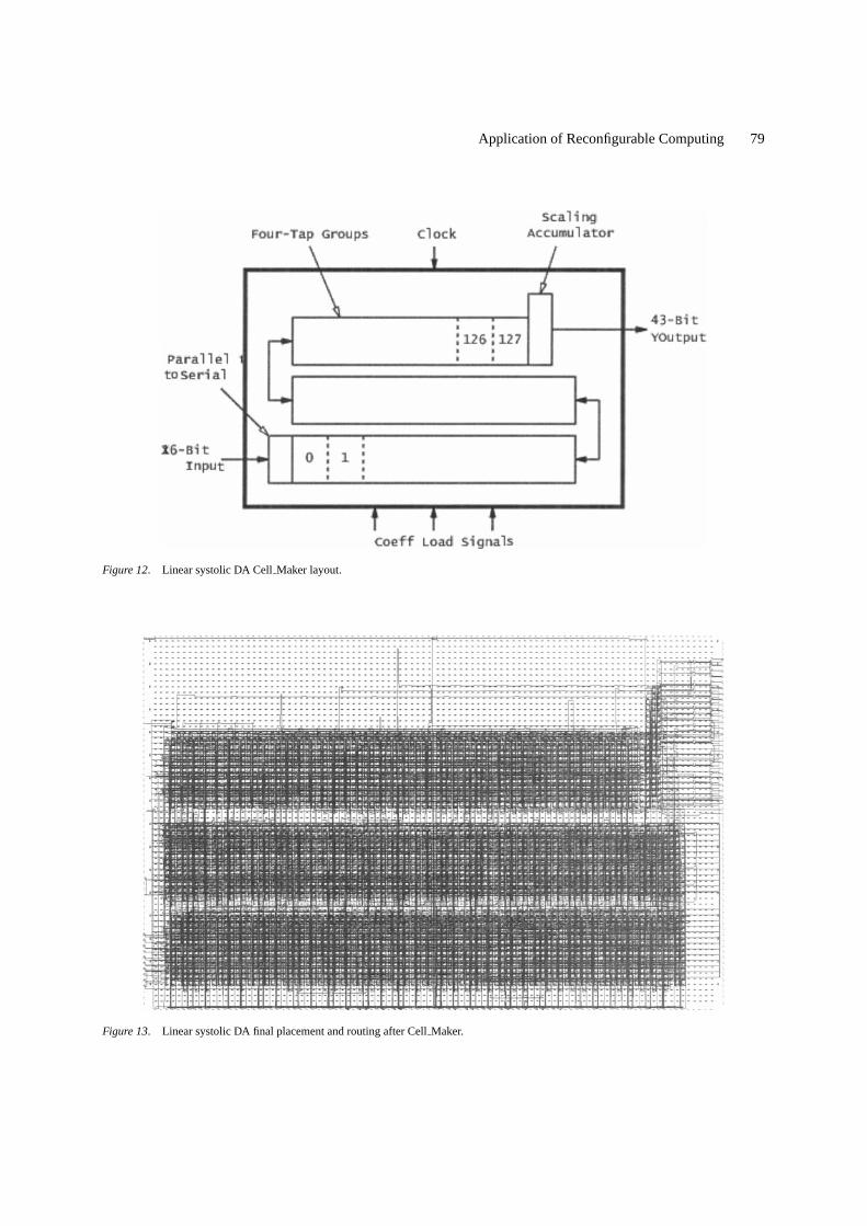
The final placed and routed design with CellMakerconstraints is shown in Fig. 13. The performance in-creased from 86 MHz to 118 MHz with the improvedsystolic layout; a 37% improvement due to layoutalone. It is also evident that the overall layout is muchmore regular and consistent with a systolic short lengthinterconnects.
The linear systolic SDA design constrained withCell Maker, as shown in Fig. 13, had a maximum clockrate of 117.5 MHz, which allowed a maximum samplerate of 7.3 MHz. With a sample rate of 7.3 MHz, and512 multiply and add operations (two operations) per-formed each clock cycle, the linear systolic DA designcould perform 7.475 GOPS. This throughput representsabout a 49% increase over the older custom VLSI de-sign described in Section 3 (with a maximum capabilityof 5.02 GOPS).
For the linear systolic DA design, about 6,700 flip-flops and shift registers were clocked; so the power con-sumption for the design was estimated at 12.14 wattswith a 117 MHz clock [19]. With 7.475 billion opera-tions performed per second at 12.14 watts, the through-put/power factor for the linear systolic DA design was0.62 GOPS/Watt. In comparison, the custom VLSI chipthroughput/power, for its 512-tap real mode, was esti-mated at 1.57 GOPS/Watt, or 2.5 times better than theFPGA linear systolic DA design.
One important lesson learned from this implemen-tation experience is that generic tools can compromisethe mapping of the desired architecture structure to theavailable FPGA hardware. For best utilization of theFPGA resources, with the goal of achieving highest
Application of Reconfigurable Computing 79
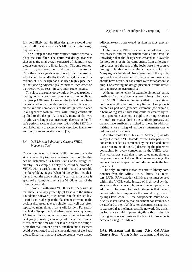
Figure 12. Linear systolic DA CellMaker layout.
Figure 13. Linear systolic DA final placement and routing after CellMaker.
80 Martinez, Moeller and Teitelbaum
Figure 14. Growth of embedded radar signal processing throughput.
performance over minimum area, the placement androuting tools should exploit architecture specificconstraints.
6. Future Candidate Applicationsfor Reconfigurable Computing Technologies
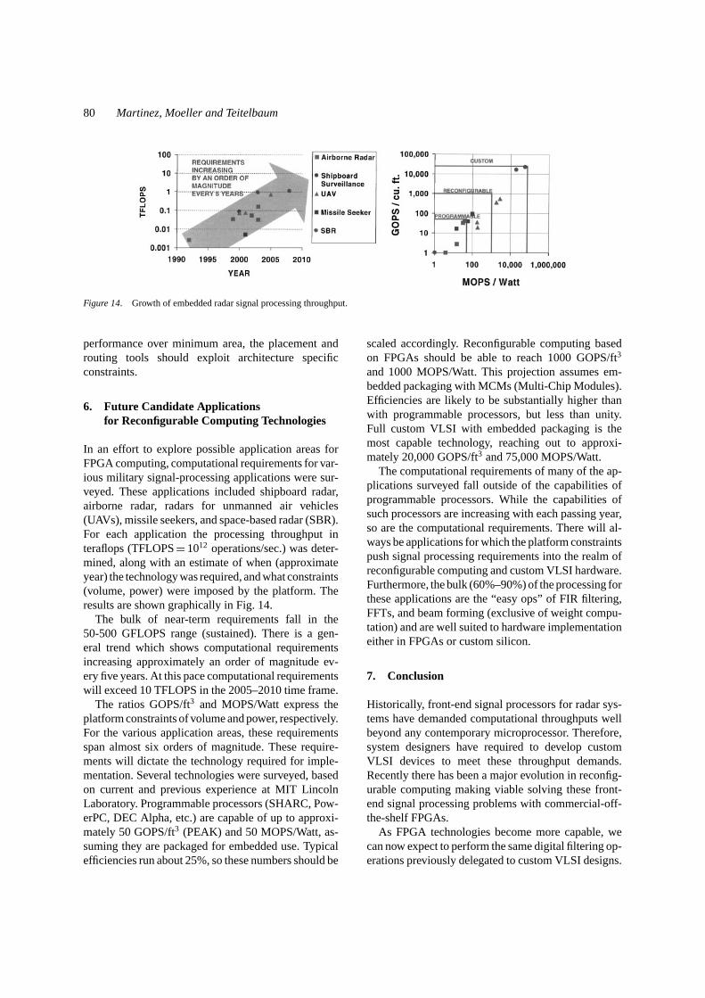
In an effort to explore possible application areas forFPGA computing, computational requirements for var-ious military signal-processing applications were sur-veyed. These applications included shipboard radar,airborne radar, radars for unmanned air vehicles(UAVs), missile seekers, and space-based radar (SBR).For each application the processing throughput interaflops (TFLOPS= 1012 operations/sec.) was deter-mined, along with an estimate of when (approximateyear) the technology was required, and what constraints(volume, power) were imposed by the platform. Theresults are shown graphically in Fig. 14.
The bulk of near-term requirements fall in the50-500 GFLOPS range (sustained). There is a gen-eral trend which shows computational requirementsincreasing approximately an order of magnitude ev-ery five years. At this pace computational requirementswill exceed 10 TFLOPS in the 2005–2010 time frame.
The ratios GOPS/ft3 and MOPS/Watt express theplatform constraints of volume and power, respectively.For the various application areas, these requirementsspan almost six orders of magnitude. These require-ments will dictate the technology required for imple-mentation. Several technologies were surveyed, basedon current and previous experience at MIT LincolnLaboratory. Programmable processors (SHARC, Pow-erPC, DEC Alpha, etc.) are capable of up to approxi-mately 50 GOPS/ft3 (PEAK) and 50 MOPS/Watt, as-suming they are packaged for embedded use. Typicalefficiencies run about 25%, so these numbers should be
scaled accordingly. Reconfigurable computing basedon FPGAs should be able to reach 1000 GOPS/ft3
and 1000 MOPS/Watt. This projection assumes em-bedded packaging with MCMs (Multi-Chip Modules).Efficiencies are likely to be substantially higher thanwith programmable processors, but less than unity.Full custom VLSI with embedded packaging is themost capable technology, reaching out to approxi-mately 20,000 GOPS/ft3 and 75,000 MOPS/Watt.
The computational requirements of many of the ap-plications surveyed fall outside of the capabilities ofprogrammable processors. While the capabilities ofsuch processors are increasing with each passing year,so are the computational requirements. There will al-ways be applications for which the platform constraintspush signal processing requirements into the realm ofreconfigurable computing and custom VLSI hardware.Furthermore, the bulk (60%–90%) of the processing forthese applications are the “easy ops” of FIR filtering,FFTs, and beam forming (exclusive of weight compu-tation) and are well suited to hardware implementationeither in FPGAs or custom silicon.
7. Conclusion
Historically, front-end signal processors for radar sys-tems have demanded computational throughputs wellbeyond any contemporary microprocessor. Therefore,system designers have required to develop customVLSI devices to meet these throughput demands.Recently there has been a major evolution in reconfig-urable computing making viable solving these front-end signal processing problems with commercial-off-the-shelf FPGAs.
As FPGA technologies become more capable, wecan now expect to perform the same digital filtering op-erations previously delegated to custom VLSI designs.
Application of Reconfigurable Computing 81
The FPGA technology offers several important benefitsto these military applications, such as:
– Reduction in design and manufacturing costs rela-tive to custom VLSI designs.
– Flexibility to implement different filtering functionsusing the same FPGA devices.
– Ability to upgrade the design to higher ADC sam-pling rates by substituting more capable FPGA de-vices commensurate with the Moore’s law progres-sion in silicon technology.
– Wider vendor sources of FPGA technologies thanavailable for custom VLSI designs.
In the past several years, FPGAs have been success-fully used for either microprocessor emulation or dig-ital control functions. For digital control functions, theFPGAs have replaced many discrete integrated circuits,simplifying the complexity and providing more flexi-bility. People have also demonstrated the applicationof FPGAs signal processing for cases where the arith-metic operations only required a few bits of precision.
In this paper, we presented a recently fielded high-performance signal processor built to provide an ag-gregate throughput of 100 GOPS based on a customVLSI design, with an input precision of 18 bits and anoutput precision of 24 bits. We used this example asan existence proof. It also provided the design goalsneeded to be demonstrated with FPGA hardware. Onlya few years back, it would have been unacceptable toattempt to solve this problem with FPGAs. This limi-tation was due to very anemic number of transistors ona die, the slow clock frequency, excessive download-ing times, inability to operate on a large data word,and poor placement and routing tools that could effi-ciently use the limited hardware available. These areashave advanced exponentially in the past years. In thispaper, we have demonstrated that the same front-enddigital filtering requirements could be met with the lat-est Xilinx Virtex XCV 1000 device, without sacrificingsystem performance.
The implementation of the digital in-phase andquadrature filtering using the custom VLSI design wasbased on a parallel group of multiply-add cells. Thisapproach was not feasible in a reconfigurable hard-ware. Instead we opted to implement the digital filteringfunction using a serial distributed arithmetic approach.This technique, previously published in the literature,offered maximum utilization of the RAM based FPGAmaintaining the throughput performance requirement.
However, we had to assist the Xilinx placementtools by creating a user constraint file (UCF) describ-ing the placement constraints for every component inthe VHDL code. This tool allowed a cell that is repli-cated many times to be placed once, and the replica-tion strategy (e.g. linear systolic) to be specified in or-der to create the best placement across the array ofCLBs.
We concluded the paper by presenting several im-portant applications with the potential to be impactedby FPGA technology. Reconfigurable computing basedon FPGAs was predicted to reach 1000 GOPS/ft3 and1000 MOPS/Watt within a couple of years, with theassumption of using embedded packaging with MCMs(Multi-Chip Modules). Throughput efficiencies werealso predicted to be substantially higher than with pro-grammable processors, but less than unity.
We do not imply that all front-end radar signal pro-cessing can be solved using reconfigurable computing.There are still system specifications, for example, inspaceborne applications, where custom VLSI solutionsare further ahead than reconfigurable hardware, partic-ularly when we need solutions with throughputs perunit power≥20 GOPS/W, data throughputs exceedingGBytes/sec, and compliant with radiation hardeningrequirements.
Acknowledgments
We would like to thank several people at MIT LincolnLaboratory for their help with various aspects of thetechnologies discussed in this paper. Bob Ford, BillSong, Michael Killoran, and Huy Nguyen providedmany insights into the application of FPGAs to front-end digital filtering. The architecture for the customfront-end radar signal processor was developed by PaulMcHugh. The custom chip specifications were pro-vided by Bob Pugh, and the design was implementedby Joe Greco. The chip was fabricated by NationalSemiconductor at the Arlington, Texas facility. Finally,the back-end chip design and design rule verificationswere performed by Mentor Graphics, Inc. The authorsare also thankful to the anonymous reviewers for theirinputs and constructive comments.
Note
1. Courtesy of Michael Killoran, MIT Lincoln Laboratory.

82 Martinez, Moeller and Teitelbaum
References
1. G.W. Stimson,Introduction to Airborne Radar, 2nd edn., ScitechPublishing, Inc., 1998.
2. J. Ward, “Space-Time Adaptive Processing for Airborne Radar,”Technical Report #1015, MIT Lincoln Laboratory, Dec. 1994.
3. A.V. Oppenheim and R.W. Schafer,Discrete-Time Signal Pro-cessing, Prentice Hall, Inc., 1989.
4. K. Teitelbaum, “A Flexible Processor for a Digital AdaptiveArray,” in Proceedings of the 1991 IEEE National Radar Con-ference, March 1991.
5. E.D. Baranoski, “Pre-Processor Specifications,” Internal Mem-orandum, 21 April 1995.
6. J. Greco, “A1000 Critical Design Review,” MIT Lincoln Labo-ratory, June 1996.
7. “Xilinx Celebrates 15th Year of Continuous Innovation inProgrammable Logic,” Xilinx Press Release, Feb. 1999,http://www.xilinx.com/company/anniversary.htm.
8. “The Future of FPGAs,” Xilinx White Paper, http://www.xilinx.com/prsrls/5yrwhite.htm.
9. K. Chapman, “Building High Performance FIR FiltersUsing KCMs,” Xilinx App Note, July 1996, http://www.xilinx.com/appnotes/kcmfir.pdf.
10. G.R. Goslin, “A Guide to Using Field Programmable GateArrays (FPGAs) for Application—Specific Digital Signal Pro-cessing Performance,” Xilinx, Dec. 1995, http://www.xilinx.com/appnotes/dspguide.pdf.
11. L. Mintzer, “Large FFTs in a Single FPGA,” inProceedings ofthe 7th International Conference on Signal Processing Applica-tions & Technology, Boston, MA, 7–10 Oct. 1996.
12. B. Allaire and B. Fischer, “Adaptive Filters in FPGAs,” inPro-ceedings of the 7th International Conference on Signal Process-ing Applications & Technology, Boston, MA, 7–10 Oct. 1996.
13. “Xilinx Core Solutions Data Book,” Xilinx, 2/98, http://www.xilinx.com/products/logicore/coresol.htm.
14. “A Simple Method of Estimating Power in XC4000XL/EX/EFPGAs,” Xilinx Application Brief XBRF014 v 1.0, June 1997,http://www.xilinx.com/xbrf/xbrf014.pdf.
15. “PowerPC 603e Microprocessors, Motorola,” http://www.moto-rola.com/SPS/PowerPC/products/semiconductor/cpu/603.html.
16. “PowerPC 750 and PowerPC 740 Microprocessors,” Motorola,http://www.motorola.com/SPS/PowerPC/products/semicon-ductor/cpu/750.html.
17. W. Song, “A Two Trillion Operations per Second MinatureMixed Signal Radar Receiver/Processor,” inAsilomar Confer-ence on Signals, Systems, and Computers, Nov. 1998.
18. T.J. Moeller and D.R. Martinez, “Field Programmable Gate Ar-ray Based Front-End Digital Signal Processing,” inIEEE Sym-posium on Field-Programmable Custom Computing Machines,FCCM’99, April 1999.
19. T.J. Moeller, “Field Programmable Gate Array for Front-End Digital Signal Processing,” Master of Engineering Thesis,Massachusetts Institute of Technology, May 1999.
20. G.R. Goslin, “Using Xilinx FPGAs to Design Custom DigitalSignal Processing Devices,” inDSPX 1995 Technical Proceed-ings, 12 Jan. 1995, p. 595.
21. G.R. Goslin, “Implement DSP Functions in FPGAs to ReduceCost and Boost Performance,” EDN, 1996.
22. B. New, “A Distributed Arithmetic Approach to Designing Scal-able DSP Chips,” EDN, 17 Aug. 1995.
23. Xilinx Publications, “The Role of Distributed Arithmetic inFPGA-based Signal Processing,” Technical Report.
24. S.A. White, “Application of Distributed Arithmetic to DigitalSignal Processing: A Tutorial Review,”IEEE ASSP Magazine,July 1989.
David R. Martinez received a B.S. degree in Electrical Engineeringfrom New Mexico State University in 1976. He received an M.S.and E.E. degree in Electrical Engineering from MIT, jointly withthe Woods Hole Oceanographic Institution in 1979. Mr. Martinezalso completed an MBA degree from the Southern Methodist Uni-versity in 1986. He worked at the Atlantic Richfield Co. in seismicsignal processing from 1979 to 1988. During this time, Mr. Martinezworked on algorithm development and technology field demonstra-tions. While at Atlantic Richfield Co., he received a Special Achieve-ment Award for the conception, management, and implementationof a multidisciplinary project. He holds three U.S. patents relating toseismic signal processing hardware. He has worked at MIT LincolnLaboratory since 1988. His areas of interest are in VLSI signal pro-cessing and high performance parallel processing systems. He hasbeen responsible for managing the development of several complexreal-time signal processor systems. Mr. Martinez is Associate Divi-sion Head in the Air Defense Technology Division. For the last threeyears, he has been the chairman for a national workshop on high per-formance embedded computing, held at MIT Lincoln Laboratory. Healso served as an Associate Editor for the IEEE Signal ProcessingMagazine.
Tyler J. Moeller grew up in Alexandria, VA, where his interestin electrical engineering was sparked over several summers of in-ternships at the Army’s Night Vision and Electro-Optics Labora-tory during High School. He then attended MIT, where he receivedhis Bachelors degree in Electrical Engineering and Computer Sci-ence. During the summers, he was an intern at MIT Lincoln Lab-oratory, where he worked on the Laboratory’s Miniaturized DigitalReceiver project, designing the digital filtering multi-chip modulefor the project. Tyler then received his Master’s degree in ElectricalEngineering and Computer Science from MIT while working on histhesis, Field Programmable Gate Arrays for Radar Front-End DigitalSignal Processing, at Lincoln Laboratory with Dave Martinez. He isnow a lead developer at carOrder.com, a spin-off company of TrilogySoftware.

Application of Reconfigurable Computing 83
Kenneth Teitelbaum received the B.S.E.E. degree in 1977 fromthe State University of New York at Stony Brook and the M.S.
degree in 1979 from the University of Illinois at Urbana-Champaign.Since then he has been employed by M.I.T. Lincoln Laboratory inLexington, MA, and currently holds the position of Senior StaffMember in the Embedded Digital Systems Group. His interests in-clude radar systems design, adaptive signal processing, and parallelcomputing.