Application of embedded frequency selective surfaces for ...
133
Scholars' Mine Scholars' Mine Masters Theses Student Theses and Dissertations Spring 2016 Application of embedded frequency selective surfaces for Application of embedded frequency selective surfaces for structural health monitoring structural health monitoring Dustin Franklin Pieper Follow this and additional works at: https://scholarsmine.mst.edu/masters_theses Part of the Electromagnetics and Photonics Commons Department: Department: Recommended Citation Recommended Citation Pieper, Dustin Franklin, "Application of embedded frequency selective surfaces for structural health monitoring" (2016). Masters Theses. 7517. https://scholarsmine.mst.edu/masters_theses/7517 This thesis is brought to you by Scholars' Mine, a service of the Missouri S&T Library and Learning Resources. This work is protected by U. S. Copyright Law. Unauthorized use including reproduction for redistribution requires the permission of the copyright holder. For more information, please contact [email protected].
Transcript of Application of embedded frequency selective surfaces for ...

Scholars' Mine Scholars' Mine
Masters Theses Student Theses and Dissertations
Spring 2016
Application of embedded frequency selective surfaces for Application of embedded frequency selective surfaces for
structural health monitoring structural health monitoring
Dustin Franklin Pieper
Follow this and additional works at: https://scholarsmine.mst.edu/masters_theses
Part of the Electromagnetics and Photonics Commons
Department: Department:
Recommended Citation Recommended Citation Pieper, Dustin Franklin, "Application of embedded frequency selective surfaces for structural health monitoring" (2016). Masters Theses. 7517. https://scholarsmine.mst.edu/masters_theses/7517
This thesis is brought to you by Scholars' Mine, a service of the Missouri S&T Library and Learning Resources. This work is protected by U. S. Copyright Law. Unauthorized use including reproduction for redistribution requires the permission of the copyright holder. For more information, please contact [email protected].
APPLICATION OF EMBEDDED FREQUENCY SELECTIVE SURFACES FOR
STRUCTURAL HEALTH MONITORING
by
DUSTIN FRANKLIN PIEPER
A THESIS
Presented to the Faculty of the Graduate School of the
MISSOURI UNIVERSITY OF SCIENCE AND TECHNOLOGY
In Partial Fulfillment of the Requirements for the Degree
MASTER OF SCIENCE IN ELECTRICAL ENGINEERING
2016
Approved by
Kristen M. Donnell, Advisor
Reza Zoughi
Ed Kinzel

2016
Dustin Franklin Pieper
All Rights Reserved

iii
ABSTRACT
This thesis proposes the use of Frequency Selective Surfaces (FSSs) as an
embedded structural health monitoring (SHM) sensor. FSSs are periodic arrays of
conductive elements that filter certain frequencies of incident electromagnetic radiation.
The behavior of this filter is heavily dependent on the geometry of the FSS and local
environment. Therefore, by monitoring how this filtering response changes when the
geometric or environmental changes take place, information about those changes may be
determined. In previous works, FSS-based sensing has shown promise for sensing
normal strain (a stretching or compressing geometrical deformation). This concept is
extended in this thesis by investigating the potential of FSSs for sensing shear strain (a
twisting deformation) and detection of delamination/disbond (defined as an air gap that
develops due a separation between layered dielectrics, and herein referred to as
delamination) in layered structures. For normal strain and delamination sensing,
monitoring of the FSS’s resonant frequency is shown to be a reliable indicator for each
phenomena, as verified by full-wave simulation and measurement. For shear strain,
simulation results indicate that an FSS may cross-polarize incident radiation when under
shear strain. Additionally, FSS was applied as a normal and shear strain sensor within a
steel-tube reinforced concrete column, where it was found to provide reliable normal
strain detection (as compared to traditional strain sensors), but was not able to detect
shear strain. Lastly, in order to improve the design procedure by reducing computation
time, an algorithm was developed that rapidly approximates the response of an FSS to
delamination through use of conformal mapping and existing frequency response
calculations.

iv
ACKNOWLEDGMENTS
First of all, thank you to my advisor, Dr. Kristen M. Donnell, for supporting me
throughout my Master’s degree, as well as helping to develop me technically and
proffesionally. Furthermore, thank you to my committee members, Dr. Reza Zoughi and
Dr. Ed Kinzel for taking the time to support me through the thesis process. Specifically,
thank you to Dr. Zoughi for providing technical support during my time in the lab, and
thank you to Dr. Kinzel for providing me the opportunity of working on this project, and
for developing the basis of this work. Furthermore, thank you to Dr. Tayeb Ghasr for
providing support in all of my lab work, and thank you to Dr. Hjalti Sigmarsson of the
ECE department at University of Oklahoma for supplying FSS samples.
In addition, thank you to everyone who I’ve had the pleasure of getting to know
throughout my graduate degree. Thank you to everyone I’ve worked with in the lab,
including Mathew Horst, Dylan Crocker, Ali Foudazi, Jaswanth Vutukury, Ashkan
Hashemi, Joseph Case, and Mojtaba Fallahpour. Furthermore, a thank you to my
wonderful non-lab friends who supported me throughout my Master’s, including my
roommates David Bubier and Edward Norris, as well as Ben Conley, Biyao Zhou, Dan
Peterson, and anyone else I awkwardly neglected to mention here, if they can forgive my
forgetfulness.
Furthermore, thank you to my dad, Darrell Pieper, for raising me and supporting
me throughout my education, as well as my mom, Susan Pieper, for helping to make me
who I am today. Additionally, thank you to my extended family for being there for me
all these years, especially my cousin Dylan Pieper for being the brother I never had.
Also, thank you to Dynetics for giving me something to do with this Master’s
degree, and thank you to all my wonderful co-workers there.
And of course, thank you to God in Heaven and our savior Jesus Christ for, well,
literally everything. And thank you to Pope Francis for being an all around cool guy.
Finally, thank you to the school, Missouri S&T, as well as the American Society
for Nondestructive Testing (ASNT) for providing financial support for my Master’s
degree, as well as for the work in this thesis.

v
TABLE OF CONTENTS
Page
ABSTRACT ....................................................................................................................... iii
ACKNOWLEDGMENTS ................................................................................................. iv
LIST OF ILLUSTRATIONS ............................................................................................ vii
LIST OF TABLES .............................................................................................................. x
SECTION
1. INTRODUCTION ...................................................................................................... 1
1.1. BACKGROUND AND RESEARCH MOTIVATION ...................................... 1
1.2. SUMMARY OF SECTIONS.............................................................................. 2
2. AN OVERVIEW OF FSS .......................................................................................... 4
2.1. A BRIEF FSS HISTORY ................................................................................... 4
2.2. BASIC FSS DESIGN AND ANALYSIS ........................................................... 5
2.2.1. Dipole-Type FSS Elements ...................................................................... 6
2.2.2. Loop-Based FSS Elements ..................................................................... 17
2.3. PRACTICAL DESIGN CONCERNS .............................................................. 23
2.3.1. Effects of Supporting Dielectrics on Frequency Response. ................... 24
2.3.2. Incident Angle. ....................................................................................... 25
2.3.2.1 Curved FSS .................................................................................28
2.3.2.2 Effect of conductors on FSS. ......................................................29
2.4. CONCLUSION ................................................................................................. 30
3. APPLICATIONS OF FSS FOR NORMAL STRAIN AND SHEAR STRAIN
SENSING................................................................................................................. 32
3.1. EFFECTS OF STRAIN ON FSS RESPONSE ................................................. 32
3.2. EFFECTS OF SHEAR STRAIN ON FSS RESPONSE ................................... 46
3.3. APPLICATION OF FSS FOR STRAIN/SHEAR/BUCKLING
DETECTION IN STEEL-TUBE REINFORCED CONCRETE
COLUMNS ...................................................................................................... 54
3.4. CONCLUSION ................................................................................................. 65
4. APPLICATIONS OF FSS FOR DELAMINATION/DISBOND SENSING .......... 67
4.1. FSS RESPONSE TO DELAMINATION WITHIN A STRUCTURE ............. 67
4.1.1. Simulation Results. ................................................................................. 68

vi
4.1.2. Measurement Results. ............................................................................ 82
4.2. DETERMINATION OF EFFECTIVE PERMITTIVITY THROUGH
CONFORMAL MAPPING .............................................................................. 90
4.3. CONCLUSION ............................................................................................... 100
5. CONCLUSION/FUTURE WORK ........................................................................ 102
5.1. SUMMARY/CONCLUSION ......................................................................... 102
5.2. FUTURE WORK ............................................................................................ 105
5.2.1. Development of FSS-Based Sensing for Shear Strain. ........................ 105
5.2.2. Development of FSS Sensor Element Design Rules. ........................... 106
5.2.3. Active FSS Element Sensing. ............................................................... 106
5.2.4. Optical Wavelength FSS. ..................................................................... 107
APPENDIX ..................................................................................................................... 108
BIBLIOGRAPHY ........................................................................................................... 118
VITA. .............................................................................................................................. 122

vii
LIST OF ILLUSTRATIONS
Page
Figure 2.1. Illustration of common FSS elements. ............................................................. 5
Figure 2.2. Dipole Array FSS with Equivalent LC Circuit ................................................ 6
Figure 2.3. Complimentary transmission response of dipole array and slot array. ............ 8
Figure 2.4. The crossed-dipole FSS. ................................................................................... 8
Figure 2.5. The Jerusalem Cross FSS (a), with associated frequency response (b) and
equivalent circuit model (c). ........................................................................... 10
Figure 2.6. Comparison of HFSS simulation and Marcuvitz analytical model of
transmission (a) and reflection (b) responses of the Jerusalem Cross FSS
design .............................................................................................................. 15
Figure 2.7. The Tripole FSS (a) and Loaded Tripole FSS (b). ......................................... 16
Figure 2.8. Examples of ring, square loop, and hexagonal loop FSSs ............................. 17
Figure 2.9. Comparison of HFSS simulation and Marcuvitz analytical model for the
transmission response of Square Loop FSS. .................................................. 19
Figure 2.10. Double square loop (left) and triple square loop (right). .............................. 20
Figure 2.11. Comparison of HFSS simulation and Marcuvitz model for the
transmission response of Double Square Loop FSS ................................... 22
Figure 2.12. The Cross Loop FSS. .................................................................................... 22
Figure 2.13. Illustration of TE and TM incidence. ........................................................... 26
Figure 3.1. Crossed-dipole FSS’s geometry (a), its transmission response as a function
of normal strain (b), and its resonant frequency as a function of normal
strain. .............................................................................................................. 34
Figure 3.2. Examples of FSS elements used for strain analysis in ................................... 36
Figure 3.3. Frequency response of the crossed-dipole FSS undergoing co-polar (a) and
cross-polar (b) normal strain. ......................................................................... 38
Figure 3.4. Grounded Tripole FSS with relevant dimensions. ......................................... 40
Figure 3.5. Grounded Loaded Tripole frequency response measurement setup. ............. 41
Figure 3.6. Parallel and perpendicularly oriented measurement results of Grounded
Loaded Tripole FSS under normal strain. ...................................................... 44
Figure 3.7. Resonant frequency of strained Grounded Loaded Tripole as a function of
polarization angle. .......................................................................................... 45
Figure 3.8. Illustration of original (top left) and sheared (bottom right) loaded tripole... 47
Figure 3.9. Co-polarization (a) and cross-polarization (b) reflection response of
Grounded Loaded Tripole as a function of shear strain. ............................... 48

viii
Figure 3.10. Simulated surface currents on Grounded Loaded Tripole FSS without
shear strain (a) and with shear strain (b). ..................................................... 50
Figure 3.11. FSS elements investigated in Figure 3.12. ................................................... 52
Figure 3.12. Simulated reflection response magnitude of cross-polarization plotted as a
function of shear strain for FSS elements of Figure 3.11. ........................... 52
Figure 3.13. Simulated Co-polarized (a) and cross-polarized (b) frequency response
for a Loaded Cross Loop FSS under shear strain......................................... 53
Figure 3.14. Cross-section of concrete column. ............................................................... 55
Figure 3.15. Diagram of linear displacement test. ............................................................ 56
Figure 3.16. Filled horn antenna for measuring FSS embedded in concrete column. ...... 58
Figure 3.17. Grounded crossed-dipole FSS (a) and grounded square loop FSS (b)
samples. ........................................................................................................ 59
Figure 3.18. Reflection responses of grounded cross FSS (a) and grounded square loop
FSS (b) in planar and curved states. ............................................................. 60
Figure 3.19. FSS samples applied to steel-tube cores. ...................................................... 61
Figure 3.20. Normal strain measured from FSS as a function of displacement. .............. 63
Figure 3.21. Comparison of normal strain data from FSS and strain gauge sensors. ....... 63
Figure 4.1. Crossed-dipole FSS (a) embedded into a delaminated structure (b). ............. 68
Figure 4.2. Reflection response of the embedded crossed-dipole FSS of Figure 4.1 for
three delamination distances. ......................................................................... 69
Figure 4.3. Resonant frequency (a) and resonant depth (b) of the embedded crossed-
dipole FSS shown in Figure. 4.1 as a function of delamination distance. ...... 71
Figure 4.4. First three resonances of dielectric structure given in Figure 4.1 (b) as a
function of delamination distance. ................................................................. 72
Figure 4.5. Dielectric structures for “Near” delamination (a) and “Adjacent to”
delamination (b) cases. ................................................................................... 74
Figure 4.6. Resonant frequency (a) and resonant depth (b) of the crossed-dipole FSS in
Figure 4.1 as a function of delamination distance for the “Near” and
“Adjacent to” delamination cases illustrated in Figure 4.5. ........................... 74
Figure 4.7. Cross Loop FSS used in multi-layer FSS structure for delamination
analysis in Figure 4.8. ..................................................................................... 77
Figure 4.8. Simulated delaminated dielectric structures, referred to as Delams 1-5. ....... 77
Figure 4.9. Simulated resonant frequencies as a function of delamination distance for
Delams 1-5 shown in Figure 4.8. The top and bottom resonances
correspond to the cross-loop FSS, while the middle resonance corresponds
to the crossed-dipole FSS. .............................................................................. 78

ix
Figure 4.10. Simulated values of resonant depth as a function of delamination distance
for Delams 1-5 (Figure 4.8). (a) and (c) correspond to the cross-loop FSS
and (b) corresponds to the crossed-dipole FSS ............................................ 79
Figure 4.11. Transmission responses for the structures shown in Figure 4.8, without
embedded FSSs. ........................................................................................... 81
Figure 4.12. Comparison of measurement and simulation of resonant frequency (a)
and resonant depth (b) of the crossed-dipole FSS as a function of
delamination distance for “Near” delamination shown in Figure 4.1. ......... 84
Figure 4.13. Measurement of resonant frequency (a) and resonant depth (b-d) of a
multi-layer FSS-integrated stackup as a function of delamination distance
for Delam 1 (Figure. 4.7 (a)). ....................................................................... 85
Figure 4.14. Measurement of resonant frequency (a) and resonant depth (b-d) of a
multi-layer FSS-integrated stackup as a function of delamination distance
for Delam 2 (Figure. 4.7 (b))........................................................................ 86
Figure 4.15. Measurement of resonant frequency (a) and resonant depth (b-d) of a
multi-layer FSS-integrated stackup as a function of delamination distance
for Delam 3 (Figure. 4.7 (c)). ....................................................................... 87
Figure 4.16. Measurement of resonant frequency (a) and resonant depth (b-d) of a
multi-layer FSS-integrated stackup as a function of delamination distance
for Delam 4 (Figure. 4.7 (d))........................................................................ 88
Figure 4.17. Measurement of resonant frequency (a) and resonant depth (b-d) of a
multi-layer FSS-integrated stackup as a function of delamination distance
for Delam 5 (Figure. 4.7 (e)). ....................................................................... 89
Figure 4.18. Coplanar line (a) and coplanar waveguide (b) configurations in a layered
dielectric structure. ....................................................................................... 92
Figure 4.19. Illustration of electric field distribution between adjacent elements for a
Square Loop FSS. ........................................................................................ 94
Figure 4.20. Square Loop FSS (a) and dielectric structure (b) used to demonstrate
approximation of εr,eff. .................................................................................. 96
Figure 4.21. Comparison of transmission response calculated from the Matlab model
and HFSS for Case 13 in Table 4.2. ............................................................. 99

x
LIST OF TABLES
Page
Table 3.1. Gauge factors for common FSS elements........................................................ 36
Table 3.2. Gauge factors of Crossed-Dipole FSS for different element dimensions. ....... 37
Table 4.1. Comparison of εr,eff calculated using the conformal mapping approach and
full-wave simulation. ....................................................................................... 96
Table 4.2. Resonant frequency for the geometry shown in Figure 4.20 as calculated
from the Matlab model and HFSS. .................................................................. 99
1. INTRODUCTION
1.1. BACKGROUND AND RESEARCH MOTIVATION
A major area of interdisciplinary research focuses on the development of
infrastructure than can provide information on its structural integrity, allowing for easier
inspection and testing [51]. As such, structural health monitoring (SHM) sensors that can
be embedded into and integrated throughout a structure are necessary. Currently, fiber
optic sensors are one of the most common embedded SHM sensors, and can sense
phenomena such as temperature and normal strain [52]. Other potential sensor
technologies involve the use of piezoelectric materials or acoustical nanowire sensors that
can be directly integrated into a structure [51], [52]. As an addition to the currently
available sensors, this thesis proposes the use of Frequency Selective Surfaces (FSS) as a
form of embedded SHM sensors.
In its most basic form, an FSS is a periodic array of conductive elements designed
to resonate at a certain frequency. At this resonant frequency, the FSS acts as either a
band-pass or a band-stop filter to incident electromagnetic radiation [1]. This filtering
behavior occurs due to inductive (L) and capacitive (C) coupling between the elements of
the FSS (and hence the FSS acts as an LC filter). This coupling, and thus the filtering
behavior of the FSS (referred to as the frequency response), is highly dependent on
geometry and local environment. As such, an FSS’s frequency response is determined by
the dimensions and spacing of the FSS elements, as well as the presence of nearby
dielectrics and conductors. This thesis proposes that an FSS’s dependence on geometry
and environment can be useful for SHM purposes. Previously, [33] and [34] have found
that an FSS can be used to sense normal strain (a stretching or compressing deformation)
[39]. The use of an FSS for sensing normal strain is extended in this work by examining
the sensitivity of different FSS elements to normal strain, as well as measurement
verification of FSS’s sensitivity to normal strain. Additionally, sensing capabilities are
explored for shear strain (defined as a twisting deformation [36]) and
delamination/disbond (defined as a separation of bonded or laminated materials within a
structure [43] and herein referred to as delamination) detection.

2
1.2. SUMMARY OF SECTIONS
Section 2 of this thesis introduces the theory and background of FSS operation
and design. A brief history of the development and research of FSS design is presented
in Section 2.1. Section 2.2 presents the fundamental theory of FSS operation, including
analysis of frequency response for various FSS elements and general design practices.
Additionally, a variety of common FSS elements used throughout this thesis are
presented and discussed. Next, Section 2.3 presents a range of more advanced FSS topics
that pertain to practical implementation, including the effects of local dielectrics and
conductors, oblique incidence of impinging radiation, and sensing using multiple FSS
layers within a single structure.
In Section 3, the use of FSSs for sensing normal and shear strain is examined. In
Section 3.1, the effects of normal strain on an FSS’s frequency response are investigated.
FSSs have previously been found to have potential as a normal strain sensor because an
FSS’s resonant frequency is a function of its geometry (conductor length, width, etc.)
[33], [34]. As such, an FSS’s resonant frequency will shift when its conductors are
stretched or compressed, as is the case when an FSS is under normal strain. By
monitoring changes in the resonant frequency, the normal strain (experienced by the FSS)
can be determined. In this investigation, the response of FSS to normal strain is
investigated for a variety of FSS elements through full-wave electromagnetic simulation
and measurements. Next, in Section 3.2, the effects of shear strain on the FSS’s
frequency response are studied through full-wave simulation for a series of common FSS
elements. These investigations are extended to a practical sensing application in Section
3.3, where the use of FSS as a normal and shear strain sensor is tested in a steel-core
reinforced concrete column.
Next, in Section 4, the use of an FSS for delamination detection in a layered
dielectric structure is explored. Section 4.1 discusses the effect of local dielectrics on an
FSS’s frequency response, as well as how a delamination in these dielectrics alters that
response. This is examined through a series of simulations and measurements that
demonstrate the use of FSSs for delamination sensing. Meanwhile, Section 4.2 presents
an analytical approximation method that uses conformal mapping to determine the
effective permittivity (εr,eff) observed by an FSS when embedded within a dielectric

3
structure. The value of εr,eff can be used to relate changes in an FSS’s resonant frequency
to changes in the surrounding dielectric environment, such as delamination. This
approach for determining εr,eff is subsequently applied to an algorithm for approximating
the frequency response of an FSS when embedded within a layered dielectric structure.
Determining εr,eff in this way reduces computation time (as compared to full-wave
simulation), allowing for expedited analysis of an FSS’s response to delamination.
Additionally, this can aid the FSS design process by approximating how an FSS’s
frequency response will be altered when embedded into a dielectric structure.
Finally, Section 5.1 summarizes the work presented in this thesis. Furthermore,
Section 5.2 outlines a number of possible extensions of this work. Such extensions
include the development of an FSS design methodology for creation of improved FSS
SHM sensors, along with the potential of active FSS and optical-wavelength FSS for
SHM sensing.

4
2. AN OVERVIEW OF FSS
This section provides an overview on the background and physical operation of
FSSs. To start, a short historical account of FSSs is presented. Then, an in-depth
discussion on the functionality and physics inherent to FSSs is provided. This discussion
includes a comparison of different FSS element geometries that are relevant to this thesis.
Lastly, problems and limitations encountered in real-world application of FSSs are
discussed.
2.1. A BRIEF FSS HISTORY
The defining feature of an FSS is its ability to act as a surface with band
pass/band stop filtering properties to incident radiation. This is accomplished through a
periodic array of conductive elements that inductively and capacitively couple when
excited by incident electromagnetic radiation (e.g., a plane wave, a propagating wave
with electric and magnetic fields that are orthogonal to each other and the direction of
propagation). One of the earliest forms of an FSS was a parabolic reflector grid using an
array of resonant dipoles that was designed and patented by Marconi and Franklin in
1919 [1]. However, much of the research into what is now referred to as FSSs didn’t
gain momentum until the 1960s and 1970s. During this time, the United States Air Force
supported classified investigations into FSS development for radar and stealth
applications [1], [2]. This research included conductive elements, such as crossed-
dipoles and tripoles, which had greater versatility than the single resonant dipoles
investigated previously. These new FSS element designs provided better performance
including insensitivity to angle of incidence (defined as the angle between a plane wave’s
direction of propagation and the direction normal to the plane of the FSS) and finer
tunability, making FSSs useful for stealth radomes and as multi-band Cassegrain reflector
dishes in antenna systems [1], [3]. After becoming declassified in the mid-1970s,
research moved towards new methods of FSS design and development for general use.
Analysis techniques such as computational modal analysis of resonating elements and
circuit model approximations of filter behavior led to a better understanding of the
physical characteristics of FSSs [3], [4]. In the 1990s and 2000s, improvements to

5
computing technology led to the use of numerical solvers, allowing for analysis of more
complicated structures that cannot be easily described through analytical means. Today,
this work has led to many different FSS designs and applications, including three-
dimensional FSS structures [5], active FSS [6], thin-film high-impedance surface
absorbers [7], and fractal element FSS designs [8].
2.2. BASIC FSS DESIGN AND ANALYSIS
As stated, the most common form of an FSS is that of a periodic array of
conductive elements. Other forms of FSSs include three-dimensional conductive patterns
and dielectric-based FSSs (both of which are beyond the scope of this thesis). A number
of popular FSS elements, such as dipoles, crosses, loops, and patches, are illustrated in
Figure 2.1.
Figure 2.1. Illustration of common FSS elements.
The frequency response of these elements to incident radiation is commonly
modeled by an equivalent LC circuit model that corresponds to the mutual inductive and
capacitive coupling that occurs between each element [3]. In this way, the FSS can be
considered as a frequency dependent impedance. Based on transmission line theory, the
impedance mismatch between the FSS LC circuit and surrounding material(s) creates

6
reflections and transmissions at the FSS interface. The net effect of these reflections and
transmissions creates the desired filtering response. Common FSS element designs tend
to fall into one or more of three types, described as dipole, loop, or patch type FSSs, or
hybridized combinations of the three [1]. Element designs used over the course of this
thesis, as well as their accompanying circuit models, are discussed next.
2.2.1. Dipole-Type FSS Elements. The simplest form of an FSS is that of the
dipole array, as shown in Figure 2.2, as well as its associated equivalent LC circuit.
g
L
W
E
C1
L1
Figure 2.2. Dipole Array FSS with Equivalent LC Circuit
When currents are excited on the FSS by a plane wave polarized along the broad
lengths of the dipoles (shown by E in Figure 2.2, with L and W defining the length and
width of the conductor), this length acts an inductance (L1), and the vertical gap between
each dipole length (of width g) provides a capacitance (C1) [1]. The desired frequency
response of the FSS can be obtained by tuning L, W, and g to obtain the corresponding L
and C values. For the dipole array FSS, the transmission frequency response is that of a
7
band-stop filter, meaning that signals can transmit through the FSS at any frequency
outside of the designated stop band, and signals having frequencies within the stop band
are reflected. The center frequency of this stop band (hereto referred to as the resonant
frequency) is dictated by the resonant length, L, of the dipole with respect to the
operating wavelength, λ. Typically, this resonance occurs when the length of the dipole
is roughly equal to half the operating wavelength, λ/2, [1]. Conversely, in order to obtain
a band-pass transmission resonance, a complementary slot-based array can be used. A
slot-based FSS is composed of an array of resonant slots cut out of a metal sheet. Unlike
conductive dipoles, these slots exhibit a band-pass resonance that occurs for an incident
plane wave polarized perpendicularly to the broad length of the slot [1]. A slot is
considered complimentary to a dipole when the dimensions of the slot match the
dimensions of the dipole, meaning that the slot FSS transmits signals at frequencies
where the dipole FSS reflects, and vice-versa. An example of transmission frequency
responses for dipoles and slots with parallel oriented incident wave polarizations
(denoted by E) is shown in Figure 2.3. This behavior is a consequence of Babinet’s
principle, and can generally be applied to most other FSS designs, if a complimentary
response is needed [1]. This consideration may be inaccurate in the presence of thick
dielectric slabs near the FSS, however, due to differences in impedance profiles between
the complimentary FSS designs. Since the dipole FSS acts as a short circuit at resonance,
and the slot FSS acts as an open circuit, the transmission lines representing the dielectric
slabs are thus loaded differently, causing non-complimentary behavior between each FSS
[3]. However, for practical use, the dipole FSS is often not used due to its strong
dependence on the polarization of an incident plane wave. Should the plane wave not be
polarized parallel to the length of the dipoles, the structure’s resonance will be reduced.
Furthermore, in the case of completely perpendicular polarization (opposite to the
polarization depicted by E in Figure 2.3), the structure stops resonating completely [3].
To help alleviate this problem, a second dipole can be added to the structure that is
perpendicular to the first dipole. This creates the crossed-dipole FSS (or Cross FSS),
shown in Figure 2.4. For this FSS, the presence of the second dipole ensures that the
polarization of an incident plane wave can never be completely perpendicular to the
length of any one conductor.

8
E
Dipole
Slot
Fre
qu
en
cy R
esp
on
se
(d
B)
Transmission
Reflection
E
Figure 2.3. Complimentary transmission response of dipole array and slot array.
E
g
LW
Figure 2.4. The crossed-dipole FSS.

9
Thus, while the resonance will still be dampened for non-parallel (to either
dipole) polarizations, the resonance will not be completely removed. Additionally, this
dampening will be less severe than for a single dipole, as both dipoles will still be
partially excited for any arbitrary polarization. The addition of the second dipole can
have adverse effects, however, in the form of an additional coupling mode that occurs
between the perpendicular arms of the cross [3]. While this coupling does not occur
when the FSS is excited by a normally incident plane wave, it does pose a problem when
the plane wave is incident at certain (off-normal) angles in which the electric field of the
plane wave is no longer parallel to the plane of the FSS (i.e., TM incidence). When this
occurs, an additional resonance is created that is very close to the main resonance of the
FSS [1]. As a result, the shape of the resonance can be significantly modified, thus
creating an unintended frequency response. To resolve this problem, an additional set of
“end-loading” dipoles can be added to the ends of each arm of the cross in order to better
control this unwanted coupling [1]. This helps to move the unwanted resonance to a
higher frequency, away from the main resonance. The addition of these end-loading
dipoles creates the Jerusalem Cross FSS, shown in Figure 2.5 (a).
In this figure, the parameters of note are the gap width (g), central conductor
length (D1) and width (W1), and end-loading conductor length (D2) and width (W2).
Additionally, an example of the frequency response and equivalent circuit model is also
shown in Figure 2.5 (b) and (c), respectively. As can be seen in the frequency response
(Figure 2.5 (b)), the presence of the new end-loading dipoles adds a second stable
transmission resonance (f2) in addition to the original transmission resonance (f0), giving
this FSS multi-resonant behavior. Furthermore, in between these two transmission
resonances there is also an impedance-controlled reflection resonance (f1), giving
additional design flexibility [13]. With this level of complexity, however, more advanced
FSS design and analysis methods must be used.
Evaluating the frequency response of any given FSS design can be accomplished
through a number of methods. These methods tend to rely on either numerical or
analytical approximations, as the coupling behavior in an FSS tends to be too complex
for direct evaluation. Numerical approximation methods, such as Method of Moments
(MoM) [9], Finite-Difference Time Domain (FDTD) [10],

10
D2 D1 W1
W2
g
f0
f1
f2
(a)
(b)
(c)
Figure 2.5. The Jerusalem Cross FSS (a), with associated frequency response (b)
and equivalent circuit model (c).
and Finite-Element Method (FEM) [11], are often used to solve for the frequency
response and field scattering of an FSS. This is accomplished by solving for the response
of a single element of the FSS (referred to as a “unit cell”) and then enforcing the effect
of periodicity using Floquet boundary conditions [55]. These boundaries operate by
analyzing the fields incident on a particular side wall of the unit cell (known as a
“master” boundary), and then matching those fields on the opposite unit cell side wall
(known as a “slave” boundary), with an additional phase term added which accounts for
the effect of the incident angle of the impinging plane wave [11]. This method results in
improved computation time (compared to modeling the full extent of a finite-sized FSS),
but can be inaccurate when applied to FSS structures that don’t have infinite (or at least,

11
effectively infinite) periodicity. Such structures include finite-size FSS (i.e. having a
limited number of elements such that edge effects from the outer-most elements can
significantly affect the response) and curved FSS structures [9]. However, these issues
can often be compensated by doing further simulations of edge cases (i.e., elements on
the edge of a finite-size FSS) or assuming locally planar behavior (for curved FSS
structures), if possible [24]. The main advantages of numerical based solutions lie in
their ability to be applied to any arbitrary FSS design, while also accounting for the
effects of incident angle and polarization of an incident plane wave. The drawback of
numerical methods, however, is the lengthy computation time required. This can become
a problem for FSS design, as design practices using this method generally involve
parameter sweeps and optimization techniques to obtain a desired frequency response.
While this isn’t necessarily a problem when fine-tuning an established design to meet
specific criteria, a more expedient solution may be needed when first starting the design
process. To help address this, a number of analytical approximation techniques have
been developed to act as a starting point for FSS design. These techniques generally
approximate FSS behavior as similar to more basic resonant structures that are easier to
describe mathematically. In doing so, equations have been developed for a number of
common FSS designs which give useful design parameters (such as the reactance of the
FSS) based on the dimensions and surrounding geometry of an FSS [13], [16], [17]. This
method of approximation often comes at the expense of neglecting the presence of more
complicated electromagnetic mechanisms (such as the effects of incident angle or
polarization), however, and thus is best suited only for initial design. While the details on
this modeling approach are discussed in Chapter 4, the analytical approximations
developed for a variety of FSS elements are discussed in this chapter, as they provide
insight into how different aspects of the geometry of an FSS contribute to the
inductance(s) and capacitance(s) in an FSS's associated equivalent LC circuit.
One such analytical method involves approximating the resonating FSS structure
as an infinitely long conductive strip grating in order to obtain the equivalent inductances
and capacitances of the FSS. Equations for the reactive and susceptive impedances of a
conductive strip grating were originally derived by Marcuvitz, and are presented in [14].

12
(2.1)
(2.2)
Equation (2.1) describes the (normalized to the impedance of free space)
inductive reactance of the strip grating when excited by a plane wave polarized parallel to
the length of the strips. Equation (2.2) describes the normalized capacitive susceptance
of the strip grating when excited by a plane wave that is polarized perpendicularly to the
length of the strips. The variables w and g describe the width of the conductors and the
width of the gaps between conductors, respectively, with p being equal to w + g.
Additionally, λ is the operating wavelength of the incoming plane wave, and θ is the
angle of incidence of the plane wave. Lastly, the function GTE,TM is given by the
following equation.
(2.3)
where A± and β are given by (4) and (5).
(2.4)
(2.5)
These equations can then be used to determine the individual capacitances and
inductances of an FSS by estimating the lengths of conductor segments as a parallel-
polarized strip grating through (2.1) and estimating the gaps between the ends of each
conductor segments as a perpendicularly polarized strip grating through (2.2). For the
case of the Jerusalem Cross in Figure. 2.5, there are five different circuit elements to be

13
calculated. The circuit elements L1 and C1 account for the first resonance, f0, and is
caused by the resonance of the main center dipole of length D1. Since the gap, g,
between the ends of the dipoles is much smaller than D1, the inductance of the FSS
structure will be nearly identical to that of an infinite strip grating. As such, the
equivalent inductance can just be found directly through (1) as being
, where p = D1 + g, and W1 is the width of the center dipole, as shown in
Figure 2.5 [13]. The term θ is not included in the function F for this case, as the effect of
incident angle is difficult to account for when these equations are used to describe an
FSS. This is due to the FSS acting as both an inductive and capacitive strip grating,
meaning that the FSS impedance is affected by both TE and TM incidence angles
(meaning that the electric field (E-field) and/or magnetic field (H-field) is no longer
perpendicular to the plane of the FSS), which isn’t accounted for in Marcuvitz’s original
equations [22]. However, [22] provides modifications that can be made to Marcuvitz’s
equations to better account for incident angle (but are beyond this scope of this thesis and
as such, are not discussed here). As such, it is assumed that θ = 0 (i.e., normal incidence)
whenever the incident angle is not specified. The capacitive term C1 represents the
capacitive coupling that occurs between the end-dipoles (of length D2) [15]. This is
described as a combination of two susceptances, Bg and Bd [13]. Bg is calculated as
approximating the horizontal (as depicted in Figure 2.5) end-dipoles as a perpendicularly
polarized strip grating of width W2 and gap spacing g, giving a susceptance of
. The
term is added to account for the fact that the end dipoles can’t be
approximated as being a continuous infinitely long conductive strip, as D2 is generally
much smaller than p. As such, the capacitance of the end-dipole is described as being
only a fraction of the capacitance seen for a strip grating [13]. The susceptance Bd is
caused by the additional coupling that occurs between the ends of the vertical end-
dipoles, and can be found as
. However, if the length
D2 is much smaller than the overall periodicity, this term can be considered largely
negligible due to the large vertical spacing between end-dipoles.
The second resonance of the Jerusalem Cross FSS is created when the end-dipoles
themselves resonate. This resonance is described by the circuit elements L3 and C3. Two

14
series combinations of these elements are placed in parallel in the circuit diagram in
Figure 2.5 (c) in order to account for the fact that there are two vertical end-caps. The
capacitance C3 is the self-capacitance of the end-dipole, which can’t be calculated using
(2) [13]. Instead, this value can be found by assuming that the resonant wavelength (λ3)
of the end-dipole is equal to
, and then using the relationship
. By finding the inductance, L, of a single end-dipole, the capacitance C3 can be
calculated. This inductance is solved using (1),
giving
. While this may seem redundant since f2 has
already been determined through this process, the values of C3 and L3 can still provide
valuable information about the quality factor of the resonant curve, as well as the
interactions of this resonance with the first resonance.
The inductance of each end-dipole, L3, is comprised of two reactances, Xl and Xm.
Xl accounts for the inductance of the two adjacent end-dipole lengths between FSS
elements, and is calculated as
. Meanwhile, Xm describes
the mutual inductance between the end-dipole and center dipole, and is calculated
as . Lastly, the capacitance C2 helps to describe the band-
stop region f1 that occurs between the resonances at f0 and f2, and is calculated as the sum
of two additional capacitances, C4 and C5. C4 is the self-capacitance of two adjacent end-
dipoles, which are treated as a single dipole of width 2W2+g. This self-capacitance is
solved in the same way as C3, with the inductive reactance now being given as
. Next, the capacitance C5 accounts for the
mutual capacitance that exists between the end-dipoles and the center dipole. This final
capacitance is given by
. Using this complete
circuit model, the response of the FSS can be determined by calculating its equivalent
admittance, Y, and this value can be subsequently used to find the reflection coefficient
(ρ), calculated as
. Additionally, the transmission coefficient (τ) is given
by [13]. A comparison of the results given between this method and
HFSS simulation [23] is shown in Figure 2.6. For this comparison, the Jerusalem Cross

15
FSS had dimensions of D1 = 17 mm, D2 = 10.3 mm, W1 = 2.3 mm, W2 = 1 mm, and g =
0.4 mm, with normal incidence assumed. Additionally, the FSS was assumed to be
located in free space (εr = 1), with no additional dielectric present.
(a)
(b)
Figure 2.6. Comparison of HFSS simulation and Marcuvitz analytical model of
transmission (a) and reflection (b) responses of the Jerusalem Cross FSS design.
16
Overall, the results of both methods shown in Figure 2.6 match fairly well. Minor
variations in resonant frequency can be seen, however, for the first reflection resonance
in Figure 2.6 (a) and second transmission resonance in Figure 2.6 (b), which demonstrate
potential inaccuracies in the approximate analytical model. Additionally, there may also
be inaccuracies in the response calculated from HFSS. However, the inaccuracies of the
HFSS model are likely minor, due to tight tolerances on the adaptive meshing of the
model during calculation. Furthermore, the depth and bandwidth of the resonances are
different between each case due to the analytical model not accounting for the surface
resistance of the FSS. Nonetheless, the analytical method is still fairly close to the
simulated results, thus demonstrating its usefulness for initial FSS design work.
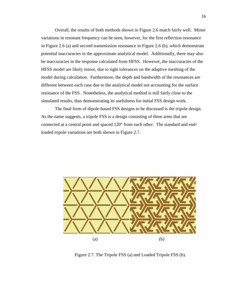
The final form of dipole-based FSS designs to be discussed is the tripole design.
As the name suggests, a tripole FSS is a design consisting of three arms that are
connected at a central point and spaced 120° from each other. The standard and end-
loaded tripole variations are both shown in Figure 2.7.
(a) (b)
Figure 2.7. The Tripole FSS (a) and Loaded Tripole FSS (b).

17
The advantage of the tripole style design is the capability to orient the elements in
a closely spaced hexagonal grid pattern. This close spacing helps reduce the sensitivity
of the FSS to incident angle (which makes the FSS’s behavior more consistent in a
practical setting, since the angle of incidence may vary) while providing a large operating
bandwidth for the transmission resonance [1]. This effect is further improved with the
addition of the end-loading conductors seen on the ends of the tripole arms in Figure 2.7
(b). This end-loading helps to reduce the size of the elements due to the added inter-
element coupling. The size reduction subsequently leads to an even closer element
spacing, resulting in a wider transmission resonance bandwidth and greater insensitivity
to incident angle [1].
2.2.2. Loop-Based FSS Elements. The next category of FSS design to be
discussed is the loop-based element. As the name suggests, these elements are formed
from loops of conductors. Examples of loop shapes include circular rings, square loops,
and hexagonal loops, as shown in Figure 2.8. Additionally, dimensions are included for
the square loop in Figure 2.8, as this element also has an analytical approximation model
that is discussed below. These dimensions are the conductor length (d) and width (s), gap
width (g), and element length (p, which is equal to d + g).
d
sg
p
Figure 2.8. Examples of ring, square loop, and hexagonal loop FSSs
18
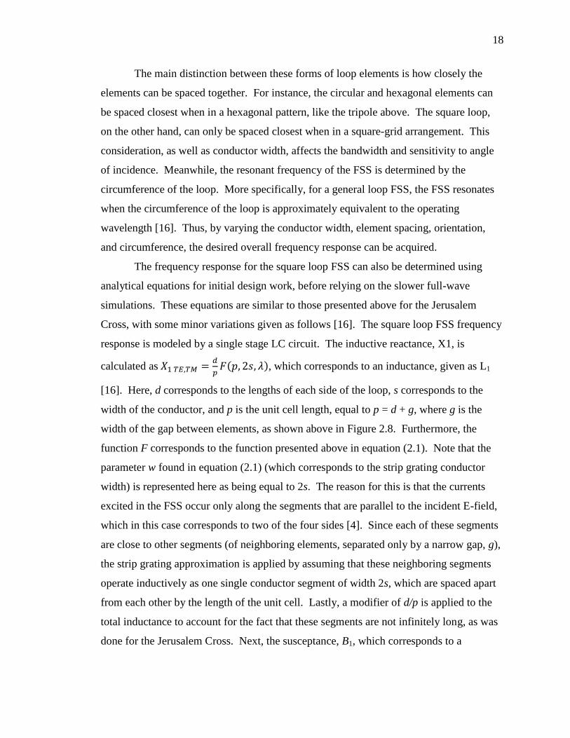
The main distinction between these forms of loop elements is how closely the
elements can be spaced together. For instance, the circular and hexagonal elements can
be spaced closest when in a hexagonal pattern, like the tripole above. The square loop,
on the other hand, can only be spaced closest when in a square-grid arrangement. This
consideration, as well as conductor width, affects the bandwidth and sensitivity to angle
of incidence. Meanwhile, the resonant frequency of the FSS is determined by the
circumference of the loop. More specifically, for a general loop FSS, the FSS resonates
when the circumference of the loop is approximately equivalent to the operating
wavelength [16]. Thus, by varying the conductor width, element spacing, orientation,
and circumference, the desired overall frequency response can be acquired.
The frequency response for the square loop FSS can also be determined using
analytical equations for initial design work, before relying on the slower full-wave
simulations. These equations are similar to those presented above for the Jerusalem
Cross, with some minor variations given as follows [16]. The square loop FSS frequency
response is modeled by a single stage LC circuit. The inductive reactance, X1, is
calculated as
, which corresponds to an inductance, given as L1
[16]. Here, d corresponds to the lengths of each side of the loop, s corresponds to the
width of the conductor, and p is the unit cell length, equal to p = d + g, where g is the
width of the gap between elements, as shown above in Figure 2.8. Furthermore, the
function F corresponds to the function presented above in equation (2.1). Note that the
parameter w found in equation (2.1) (which corresponds to the strip grating conductor
width) is represented here as being equal to 2s. The reason for this is that the currents
excited in the FSS occur only along the segments that are parallel to the incident E-field,
which in this case corresponds to two of the four sides [4]. Since each of these segments
are close to other segments (of neighboring elements, separated only by a narrow gap, g),
the strip grating approximation is applied by assuming that these neighboring segments
operate inductively as one single conductor segment of width 2s, which are spaced apart
from each other by the length of the unit cell. Lastly, a modifier of d/p is applied to the
total inductance to account for the fact that these segments are not infinitely long, as was
done for the Jerusalem Cross. Next, the susceptance, B1, which corresponds to a

19
capacitance, given as C1, is calculated as
. Given these
equations, the frequency response can be calculated from the resultant impedance, the
result of which is compared with HFSS simulation in Figure 2.9. For this comparison,
the square loop was designed to have parameters of d = 10 mm, s = 2 mm, g = 2 mm, and
p = 12 mm.
Figure 2.9. Comparison of HFSS simulation and Marcuvitz analytical model for
the transmission response of Square Loop FSS.
As shown in Figure 2.9, the simulation and analytical model results match well.
This again indicates the usefulness of analytical equations for FSS design due to its low
computational requirements (when compared to full-wave simulation).
One unique advantage of the loop-type elements is the ability to incorporate
higher frequency resonant structures into the FSS design. This is accomplished by
adding additional rings into the interior of the initial outer ring. Since the resonant

20
frequency of these structures is related to the circumference of the rings, these interior
rings add additional resonances to the frequency response [17], [18]. Examples of double
and triple square loop FSSs are shown in Figure 2.10. Dimensions are included for
double square loop for the analytical model below, and include the outer conductor length
(d1) and width (s2), outer gap width (g1), inner conductor length (d2) and width (s2), inner
gap width (g2) and element length (p, which is equal to d1+g1)
g1g2s1 s2
d1
d2
p
Figure 2.10. Double square loop (left) and triple square loop (right).
For the double square loop FSS design, the inductance of the inner square loop
operates similarly to that of the single square loop, but its capacitance is affected by the
outer loop. Meanwhile, the capacitance of the outer loop is reduced from that of the
single loop design, and the reactance of the outer loop is affected by an additional
inductance created by the width of the inner conductor loop, as is shown in the following

21
equivalent circuit approximation equations [17]. The equivalent circuit for the double
square loop FSS is composed of two series LC circuits in parallel with each other (which
corresponds to the double-resonant nature of the FSS). The value of L1 for the first
resonance is calculated as a parallel combination of two other inductances that
correspond to the inductances created by the conductor lengths of both the inner and
outer loop, given here as Li and Lo, respectively. These inductances are calculated as
and . The total reactance for L1 can then be calculated as
, where d1 is the side-length of the outer loop, p is the unit cell length
p=d1+g1, g1 is the gap between neighboring outer square loops, and s1 and s2 are the
widths of the outer and inner square loops, respectively.
The value for L2 for the double square loop is calculated in a manner similar to L2
of the single loop above, with the associated reactance for L2 calculated as
, where d2 is the side-length of the inner loop. Next, the susceptances
corresponding to C1 and C2 are calculated based on the values of two separate
capacitances, Ci and Co, which are related to the inner and outer conductor rings,
respectively. The capacitance Ci is calculated as (with g2 being the gap
between each square loop) and Co is calculated as . From these, the
susceptance for C1 is calculated as
and the susceptance for C2 is
calculated as
. The resulting frequency response of this circuit-based
analytical model is compared to simulation results in Figure 2.11. For this comparison,
the dimensions of the double square loop were set as d1 = 4.8 mm, w1 = g1 = w2 = 0.2
mm, d2 = 3.5 mm, g2 = 0.45 mm, and p = 5 mm.
Overall, the results obtained by HFSS and the circuit approximation model
equations have comparable resonant behavior. More specifically, the resonant
frequencies from both methods differ by approximately 1 GHz. Although not exact,
these circuit approximations can still be useful for an initial estimate of an FSS’s
frequency response when first developing an FSS. The loop concept can also be applied
to other FSS types, creating hybrid elements, such as the Cross Loop FSS shown in
Figure 2.12.

22
Figure 2.11. Comparison of HFSS simulation and Marcuvitz model for the
transmission response of Double Square Loop FSS.
λ/4
E
jZo tan(βl)
l
Zo ZL = 0
Figure 2.12. The Cross Loop FSS.

23
The main advantage given by this hybridized design is that the overall element
size can be reduced. This is possible because the arms that aren’t parallel to the E-field
of the incoming wave instead act as an inductive impedance. This impedance occurs due
to the arms acting as a two-wire transmission line loaded with a short (of load impedance
ZL = 0Ω) at the end. This gives a reactive response based on the length of the arms, l, as
well as the effective impedance of the two-wire transmission line, given as Zo. If the
lengths of all four arms are assumed the same, then at resonance, the length l will be
equal to λ/8, giving an inductive response [1]. This inductance essentially makes up for
the inductance lost by the reduction in the length of the element, thus allowing the
element to be made smaller while still operating at a fixed frequency. Another advantage
given by this design is that the bandwidth of the resonance can be easily controlled by
changing the impedance, Z0, of the two-wire transmission line [1]. This can be changed
by tuning both the conductor width of the element, as well as the interior spacing between
each line, thus giving a number of design parameters that can be adjusted without
affecting resonant frequency, making the Cross Loop FSS a highly versatile design.
Naturally, many other hybridized designs can also be created by combining elements of
different FSS designs. However, this is beyond the scope of this thesis and is not
discussed here.
2.3. PRACTICAL DESIGN CONCERNS
While the shape and dimensions of an FSS element plays the greatest role in
determining the frequency response of the FSS, the overall response is also affected by
other factors. For example, practical concerns, such as the presence of a supporting
dielectric layer (upon which an FSS may be etched), or the incident angle of an
impinging plane wave can cause the resonant frequency to drift or be dampened. Other
environmental concerns, such as the presence of a ground plane near the FSS or curvature
of the FSS, can more drastically alter the frequency response. As a result, these structure-
dependent concerns must be evaluated to understand how an FSS will behave in a real-
world system. As such, it may be possible to design an FSS in order to counteract or
even take advantage of these effects. Thus, the mechanisms behind these environmental
and practical effects will now be discussed.

24
2.3.1. Effects of Supporting Dielectrics on Frequency Response. One common
concern when implementing an FSS in a structure is how the structure itself will affect
the FSS response. Such a structure can include the dielectric substrate that the FSS is
printed on, any dielectric structural materials that surround the FSS, and the presence of
conductors (which will be discussed in a separate section). The presence of dielectric
layers around an FSS can affect the frequency response in two ways. First, a dielectric
near the FSS will directly increase the capacitance of the FSS [19]. The increase in
capacitance caused by this dielectric loading will then reduce the resonant frequency of
the FSS, while also changing the depth and bandwidth of the resonance. The resonance
bandwidth is changed because the capacitance is affected by the permittivity of the
material, but the inductance is not. Conversely, if the material is magnetic (not typical
for an FSS substrate), then the inductance will also increase (as well as the capacitance,
depending on the material’s permittivity). Additionally, the degree to which the
capacitance of the FSS is increased is related to the thickness of the dielectric, as well as
its proximity to the FSS. If a dielectric layer completely surrounds an FSS on both sides,
and is thicker than approximately 0.4p (where p is the length of the unit cell), then the
capacitance is multiplied by the relative permittivity, εr, of the material [2]. However, if
the material is very thin compared to the dimensions of the FSS, or if there are multiple
materials surrounding the FSS, then the change in capacitance won’t be purely related to
the permittivity (εr) of any one material. Instead, the capacitance of the FSS is shifted by
a modified permittivity that is referred to as the effective (relative) permittivity, εr,eff [19].
For example, if different materials of appropriate thickness (such that all capacitive
coupling from the FSS occurs within them) are present on each side of the FSS, then the
value of εr,eff is calculated as an average between the permittivity of the materials on
either side of the FSS. In the case of a thick dielectric present on one side of the FSS
only, the value of εr,eff will be the average of the permittivity of the material and of free
space, which leads to
[20]. However, for the case of a very thin dielectric
near the FSS, the calculation of εr,eff becomes more difficult since the value of εr,eff does
not change linearly with the thickness of the dielectric. The reason for this is that the
majority of the electric field coupling in the FSS occurs directly at the surface of the FSS,
and falls off non-linearly with distance from the FSS [19]. Furthermore, the complexity

25
of calculating εr,eff is further increased if multiple layers of thin dielectrics are present.
The treatment of this problem as it relates to FSS design is discussed later in Section 4.
The presence of a multi-layer dielectric can also have a passive effect on the frequency
response when measuring an FSS. That is to say, a layered dielectric structure alone will
also lead to additional resonant behavior due to the presence of reflections at interfaces
between different dielectrics [19]. If this additional resonant response occurs near the
operating frequency of the FSS, FSS measurement may become more difficult, as the
presence of these dielectric resonance(s) may potentially hide the resonance of the FSS.
Depending on the characteristics and requirements of the structure in which the FSS is
embedded, this issue can be counteracted in a number of ways. First, if a portion of the
structure does not have an FSS present, this portion can be used to isolate the response of
the structure itself. With this data, the response of the structure can be removed from the
overall frequency response (including the FSS response), thus yielding the effect of the
FSS alone. Alternatively, if needed, the use of an active FSS can be employed. This
form of FSS can essentially be designed to have its resonance switched on or off using,
for example, PIN diodes properly connected throughout the surface of the FSS [6]. By
modulating between the on and off states of the FSS resonance, the resonance of the FSS
can be resolved from other resonances in a structure.
2.3.2. Incident Angle. In an ideal system, an FSS will be excited by normally
incident radiation. However, in a real-world application, the propagation direction may
not be known or controllable. As such, an FSS may need to be designed to operate under
a wide range of incidence angles. However, the effect of incident angle on FSS operation
is often complicated, making it difficult to calculate the FSS response through analytical
means. As such, when incident angle is a concern, full-wave simulation will generally be
required in order to understand how the frequency response of the FSS will be affected.
However, most basic FSS elements have a similar response to incident angle. In general,
incident angle will affect the frequency response of an FSS in two ways, depending on
whether the mode of incidence is as a TE or TM wave. A visual representation of these
modes is shown in Figure 2.13. Blue arrows indicate E-field direction for each incidence
definitions, while green arrows indicate the magnetic field (H-field). Meanwhile, black

26
arrows indicate direction of propagation (DOP), while θ and φ indicate angle of TE and
TM incidence, respectively.
E
X
Z
Y
Normal
HE
TM
H
TE
H
E
φ θ
DOP
DOPDOP
Figure 2.13. Illustration of TE and TM incidence.
For a TM incident wave, the incident angle of the incoming plane wave causes a
portion of the electric field to be normal to the plane of the FSS, with the magnetic field
remaining completely parallel to the plane of the FSS. As a result, the resonance of the
FSS tends to become dampened, with stronger dampening occurring for higher angles of
incidence. This happens due to the occurrence of larger phase differences between

27
adjacent elements [3]. For TE incidence, the magnetic field has a vector component that
is normal to the plane of the FSS, while the electric field remains parallel to the plane of
the FSS. When this type of incidence occurs, the resonant frequency of the FSS will
generally be shifted, usually without noticeably affecting resonant bandwidth. This
occurs because incident angle-induced phase differences occurring along the parallel-
polarized length of the FSS will cause the FSS to behave as though it were longer, thus
shifting the frequency of the FSS [21]. Lastly, if the electric and magnetic fields of an
obliquely incident plane wave both have some component normal to the plane of the FSS,
a combination of TE and TM mode effects will occur, changing the frequency and depth
of resonance. As such, since these effects may alter the expected frequency response of
the FSS, a number of corrective measures may be needed.
For most cases, two common design practices can be implemented to mitigate the
effects of incident angle on the resonant response of an FSS. First, when designing the
FSS, it is often considered good practice to orient the elements of the FSS to ensure a
minimal (or reduced) element spacing [1]. By doing this, the distance between elements
can be minimized, thus reducing the effect of phase difference between elements caused
by incident angle. Naturally, some elements are easier to arrange closely than others, and
are considered more desirable to use should incident angle be a consideration. A few of
these elements, as discussed in section 2.2, include the various loop type elements [21].
Other hybridized elements (such as the Jerusalem Cross) can also provide a greater
insensitivity to incident angle. The second method that can be used to reduce the effects
of incident angle involves strategic use of dielectric layers that can surround the FSS [3].
If a dielectric layer is placed between the FSS and the incident plane wave source, the
incident angle seen by the FSS will be reduced due to Snell's Law [19]. That is to say, at
the interface between the dielectric layer and the surrounding environment (generally
assumed to be air), the incident plane wave will be refracted closer to the plane of the
FSS due to the permittivity of the dielectric, reducing the incident angle.
Generally, it is ideal for the thickness of the supporting dielectric to be a multiple
of λ/4 in order to reduce the effect of its impedance and corresponding reflections
through quarter-wave transformation [1]. However, it may not always be possible to
control the dimensions of the support structure surrounding the FSS, meaning that the

28
dielectric structure may cause additional resonances in the frequency response. As such,
the effects of both the presence of the material and the incident angle will need to be
accounted for in this case. Lastly, the use of a dielectric for incident angle compensation
is generally more effective for TE incidence, rather than for TM incidence. This is due to
the effectiveness of the dielectric being reduced for TM incidence as the angle of
incidence approaches the Brewster Angle, where the interface between the dielectric and
air no longer reflects. In this case, the λ/4 dielectric thickness specification becomes a
requirement [21].
2.3.2.1 Curved FSS. Another concern for the implementation of an FSS in a
practical system occurs when the FSS needs to be conformed to a curved structure.
Examples of applications where an FSS may be curved include sub-reflector antenna
dishes and stealth radome structures [24]. When an FSS is curved, a number of changes
in the FSS’s frequency response can occur, depending on the nature of the curvature.
Geometrically speaking, there are two forms of curvature to take into account [27]. First,
there is the singly-curved FSS, which conforms to the shape of a cylinder. Secondly,
there is the doubly-curved FSS, which is conformed to a spherically or conically rounded
surface, such as a nose cone on an aircraft. Naturally, the effect of double-curvature on
the frequency response is more severe than that of the single-curvature. In either case,
however, the overall effects of curvature are similar. In general, a curved FSS will have
an altered resonant response from an equivalent planar FSS. This occurs due to a
reduction of impedance in the FSS resulting from changes in FSS coupling caused by the
curvature. In addition, the effect of curvature causes there to be a different incident angle
amongst the elements of the FSS, causing differences in both phase and magnitude for
each of the elements over the FSS surface [25]. This is exacerbated further by the fact
that the curvature will also cause the plane wave to reach some portions of the FSS before
others, adding another degree of variation in phase difference over the FSS [25]. Another
concern with a curved FSS is the possibility of coupling between non-adjacent elements,
as the geometry of the curvature causes the distance between non-adjacent elements to
become shorter [24]. As a result, the currents excited on the elements of the FSS may be
significantly altered [25]. Simulations may also be difficult when designing a curved
FSS, as periodic unit cells can no longer be used in standard simulators, since the

29
curvature breaks the periodicity of the FSS. As a result, in order to obtain an accurate
simulated frequency response, the entire structure of the curved FSS may have to be
simulated. Thus, simulations may take an extensive amount of time or be impossible due
to computational limitations [26]. As such, it may be necessary to utilize planar
approximations (as long as the curvature is not extreme and the effects of phase and
incident angle can be accounted for [26]). Another strategy may be to use well-
established FSS element designs that respond well to curvature (such as the circular ring
[27]), such that the simulated planar response provides enough design validation to
support the building and testing of a curved FSS.
2.3.2.2 Effect of conductors on FSS. The final structural consideration to be
discussed is the presence of a conductive ground plane or additional FSS layers on the
response of an FSS. When an FSS is embedded into a structure with a ground plane, a
transmission response is no longer possible. Instead, the grounded FSS acts as an
absorber, giving a reflection resonance at a prescribed frequency. This absorbing
behavior occurs due to the FSS acting as a high-impedance surface (HIS), essentially
acting as a matched load at resonance, with energy being absorbed by the resistivity of
the FSS and through the loss in the dielectric substrate [7]. When the ground plane is
considered “far” from the FSS (such that there is no coupling between them), an
additional parallel inductance is created by the conductor-backed dielectric, acting as a
transmission-line impedance [28]. To control the resonant response of the FSS, this
additional inductance must be compensated for by using a highly capacitive FSS element,
such as a patch. Additionally, since the impedance of the FSS isn't directly affected by
the ground plane, the effect of the ground plane on the overall frequency response can be
accounted for with transmission line theory, assuming the impedance of the FSS is
known [28]. This is done by treating the ground plane as a shorted load at the end of a
transmission line separating the ground plane and FSS. However, when the ground plane
is located closer to the FSS, the FSS will begin to couple to the ground plane. In doing
so, the capacitance of the FSS will increase, while the inductance decreases [27]. This is
caused by the reduction of the gap between FSS and ground restricting the magnetic field
(H-field) coupling around the FSS while increasing E-field coupling between the FSS and
ground. In this arrangement, the use of highly capacitive elements will no longer be

30
needed to account for the higher inductance. Instead, traditional dipole and loop
elements can be used [27]. The disadvantage of this arrangement, however, is that the
complexity of the FSS now requires the use of simulation for design work, as no simple
analytical model for a ground plane coupled FSS is readily available. Despite this minor
design issue, HIS FSS designs have proven invaluable for use as thin absorbers in
embedded antenna and stealth applications [1], [3].
If a second FSS should be present in a structure, the above behaviors become
more complicated. Naturally, when two separate FSS layers are far from each other, the
overall response can again be determined using transmission line theory, with each FSS
acting as an individual reactive impedance separated by dielectric layers that act as
transmission line segments [30]. However, when these FSS layers are moved near each
other, they begin to couple. This coupling is much more complicated than that of the
ground plane since the coupling is highly dependent on the different FSS geometries. As
such, there is a fair degree of difficulty in predicting the resultant FSS responses outside
of numerical simulation [30]. Due to this significant complexity, this type of FSS
configuration won't be discussed in detail here, and will instead be left for future
investigations. Instead, only non-coupling multi-layer FSS's will be used for the
purposes of this thesis.
2.4. CONCLUSION
In this section, FSS history, theory, and operation were presented. Several
examples of common FSS elements were used to highlight the geometrical dependence of
the FSS’s resonant filtering behavior. Additionally, a variety of FSS frequency response
calculation methods were discussed, including full-wave simulation and analytical
approximations. Finally, a number of issues for practical implementation of FSS were
considered, such as the effects of incident angle, FSS curvature, and the presence of
dielectrics and conductors local to the FSS.
In summary, the reflection/transmission response of an FSS is affected not only
by the geometry of the conductors of the FSS, but also by the nature of the structure in
which the FSS is embedded. For any given FSS, incident energy is either reflected or
transmitted over certain frequencies due to inductances and capacitances generated

31
between elements of the FSS. These inductances and capacitance values are determined
by the dimensions of the FSS geometry, such as conductor length and width and gap
width. Additionally, the frequency response of the FSS can be altered by nearby
dielectrics and conductors, incident plane wave orientation, and FSS curvature. By
observing how the response of an FSS is affected by these geometrical considerations,
correlations (such as the effect of geometry on resonant frequency or resonant band-
shape) can be drawn, linking geometrical effects to the resultant frequency response.
Thus, if the geometry of an FSS embedded in a structure is deformed due to stresses in
that structure, the nature of these geometrical deformations may be determined from the
resultant change in frequency response. Based on this observation, FSSs may find
application for structural health monitoring purposes by taking advantage of their
geometrical dependencies. From this perspective, the potential applications of FSSs as
embedded sensors are investigated through the rest of this thesis.

32
3. APPLICATIONS OF FSS FOR NORMAL STRAIN AND SHEAR STRAIN
SENSING
In this section, the effects of normal and shear strain deformation are investigated
for a variety of common FSS designs. Since the frequency response of an FSS is heavily
geometry dependent, deformation of this geometry will alter the frequency response. As
such, by understanding how the frequency response of a given FSS is modified by
geometry-altering deformations, it may be possible to use FSS’s as both surface-mounted
and embedded structural health monitoring (SHM) sensors. That is, if an FSS is installed
on a structure that undergoes mechanical stress, both the structure and the embedded FSS
will be similarly deformed. Thus, the changes in the frequency response of the FSS
brought on by this deformation (and subsequently the normal and/or shear strain) can be
monitored remotely by interrogating the FSS using an external measurement system.
Thus, since the mechanical state of the structure can be remotely interrogated using FSS-
based sensors, the structure can be considered a “smart structure” that has inherent SHM
capabilities [35].
The use of an FSS as an SHM sensor was first applied for normal strain detection
in [31], [32], [33], and [34]. With this work in mind, the measurement of normal strain
with FSS’s is discussed in Section 3.1. Meanwhile, Section 3.2 focuses on utilizing
FSS’s to characterize shear strain. Finally, Section 3.3 discusses the application of FSSs
to SHM of steel-tube reinforced concrete columns.
3.1. EFFECTS OF STRAIN ON FSS RESPONSE
The first type of deformation to be discussed is that of normal strain. Normal
strain is defined here as being a stretching or compressing deformation of a material
caused by an applied force. Normal strain is quantified as a unitless vector having a
magnitude and direction [39]. The magnitude of the normal strain is defined as a ratio of
the length of the stretched/compressed structure in relation to the original, non-strained
structure. For example, a bar that has increased to 1.5 times its original length is said to
have 0.5 normal strain. Furthermore, the polarity of this normal strain value indicates
whether tension or compression is taking place, with tension (i.e., an increase in length)
resulting in positive normal strain and compression (i.e., a decrease in length) resulting in

33
negative normal strain. Additionally, the normal strain also has a directional component
associated with it, describing the vector (direction) along which the normal strain is
taking place [32].
In Section 2, it is stated that the resonant frequency of an FSS is primarily
dependent on the conductor lengths within the FSS. That is, as the length of a conductive
element increases or decreases, the resonant frequency of this conductor respectively
decreases or increases due to the relation between operating wavelength (λ) and
conductor length. Therefore, it is expected that a similar shift in resonant frequency will
occur if the length of this conductor were altered by normal strain [31]. Whether the FSS
dimensions are either lengthened or shortened depends on the polarity of the normal
strain (i.e., tension or compression). Furthermore, the direction of the normal strain
vector dictates what aspects of the FSS’s geometry are deformed, which has subsequent
ramifications on the frequency response. For this investigation, it is assumed that all
normal strain occurs parallel to the plane of the FSS. This is because normal strains
oriented orthogonal to the plane of the FSS produce no noticeable effect on the geometry
of the FSS (and related frequency response), and thus are not considered.
The effect of normal strain on the resonant response of an FSS can also be
described from a circuit element perspective by modeling the FSS as a band-pass or
band-stop RLC filter circuit (composed of resistors, capacitors, and inductors which
represent the coupling and surface resistance of the FSS). In an RLC filter circuit, the
resonant frequency (f0) is calculated as f0 = 1/(2πLC), where L and C are the inductance
and capacitance of the circuit. Meanwhile, the resistance, R, of the filter determines the
depth of the filter’s resonance. When an FSS undergoes normal strain, the L and C
values of the FSS are altered. For instance, as the length of an FSS’s conductor
increases, the associated L also increases. Conversely, as the distance between
conductors is increased, C decreases due to a reduction in electric field coupling.
Meanwhile, the surface resistance of the FSS remains effectively unaltered by normal
strain, barring minor changes due to an increase in the conductor surface area (not
considered in this investigation). Taken together, these changes in L and C collectively
alter the resonant frequency, while the depth of the FSS’s resonance remains unchanged
due to the unaltered R. To illustrate this, an example of a crossed-dipole FSS under

34
normal strain is shown in Figure 3.1 (a). Additionally, the simulated (using HFSS [23])
transmission responses for different values of normal strain are given in Figure 3.1 (b),
while the resonant frequency of this FSS is plotted as a function of normal strain in
Figure 3.1 (c). The polarization of the incident plane wave is assumed parallel to the
direction of normal strain, as indicated by the vector labeled ‘E’ in Figure 3.1 (a), unless
otherwise specified.
(a) (b)
(c)
Figure 3.1. Crossed-dipole FSS’s geometry (a), its transmission response as a function of
normal strain (b), and its resonant frequency as a function of normal strain.

35
In Figure 3.1 (b), the FSS’s resonant frequency is shown to decrease
proportionally with normal strain, with the resonant depth remaining relatively
undisturbed. Furthermore, the frequency shift follows a linear relationship with the
normal strain, as shown in Figure 3.1 (c). This occurs because the resonant wavelength
(λ) is linearly related to the length of the dipoles in the Crossed-dipole FSS, which
resonates for a dipole length equal to λ/2. However, this linearity may not always be true
for all element types. The sensitivity of an FSS’s resonant frequency to normal strain can
be quantified by considering its gauge factor, ς, which relates normal strain to change in
resonant frequency, and is calculated using Equation 3.1 [35].
(3.1)
Here, Δf is the change in resonant frequency for a given change in normal strain, Δs [35].
Furthermore, this value is normalized by the FSS’s un-deformed resonant frequency (f0)
so that the sensitivity of FSSs with different resonant frequencies to normal strain can be
compared directly. For the FSS of Figure. 3.1, ς was calculated as 0.51, based on the
resonant frequency shift determined using full-wave simulation. Naturally, since
different FSS designs have different dependences between geometric dimensions and
resonant wavelengths, each FSS will have its own value of ς. As such, the normalized ς
values (calculated through simulation) for a variety of FSSs (shown in Figure 3.2) are
presented in Table 3.1. Note that grounded FSS’s are defined here as having a ground
plane 0.127 mm below the FSS.
Based on Table 3.1, dipole-type FSSs (such as the Crossed-dipole, Jerusalem
Cross, and Tripole FSSs) have similar ς values. Meanwhile, the square loop element has
a smaller ς, making it less sensitive to normal strain and therefore potentially unsuitable
for strain sensing purposes. Additionally, grounded FSSs have a higher ς than their
ungrounded counterparts, making the addition of a ground plane advantageous if it can be
included in a structure. It should be noted that ς for these FSS elements is only
representative of these specific elements, and therefore may vary if the dimensions of the
element are changed. As such, to investigate the effect of FSS dimensions on ς, a
simulation was conducted in which the conductor length, conductor width, and gap width

36
of a crossed-dipole FSS were each varied over a range of normal strains. The resulting ς
is reported below in Table 3.2.
Crossed-Dipole FSS Jerusalem Cross FSS Cross-Loop FSS Loaded Cross-Loop FSS
Square Loop FSS Tripole FSS Loaded Tripole (Grounded and Ungrounded) (Grounded and Ungrounded)
Strain
Direction
Parallel
Polarization
E
Figure 3.2. Examples of FSS elements used for strain analysis in Table 3.1.
Table 3.1. Gauge factors for common FSS elements.
FSS Elements Gauge
factor (ς)
Crossed-Dipole 0.53
Jerusalem Cross 0.54
Square Loop 0.18
Tripole 0.68 Grounded Tripole Loaded Tripole Grounded Loaded Tripole
0.74 0.56 0.7
Cross Loop 0.57
Loaded Cross Loop 0.52
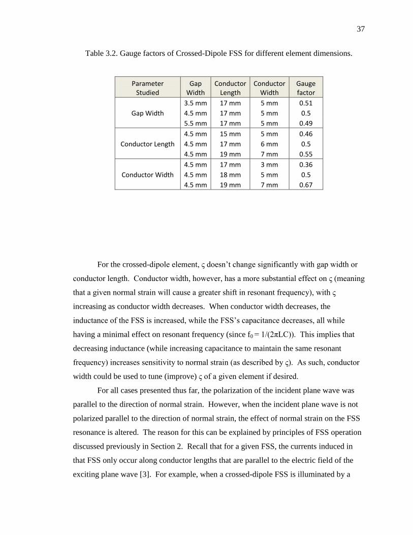
37
Table 3.2. Gauge factors of Crossed-Dipole FSS for different element dimensions.
Parameter Studied
Gap Width
Conductor Length
Conductor Width
Gauge factor
3.5 mm 17 mm 5 mm 0.51
Gap Width 4.5 mm 17 mm 5 mm 0.5
5.5 mm 17 mm 5 mm 0.49
4.5 mm 15 mm 5 mm 0.46
Conductor Length 4.5 mm 17 mm 6 mm 0.5
4.5 mm 19 mm 7 mm 0.55
4.5 mm 17 mm 3 mm 0.36
Conductor Width 4.5 mm 18 mm 5 mm 0.5
4.5 mm 19 mm 7 mm 0.67
For the crossed-dipole element, ς doesn’t change significantly with gap width or
conductor length. Conductor width, however, has a more substantial effect on ς (meaning
that a given normal strain will cause a greater shift in resonant frequency), with ς
increasing as conductor width decreases. When conductor width decreases, the
inductance of the FSS is increased, while the FSS’s capacitance decreases, all while
having a minimal effect on resonant frequency (since f0 = 1/(2πLC)). This implies that
decreasing inductance (while increasing capacitance to maintain the same resonant
frequency) increases sensitivity to normal strain (as described by ς). As such, conductor
width could be used to tune (improve) ς of a given element if desired.
For all cases presented thus far, the polarization of the incident plane wave was
parallel to the direction of normal strain. However, when the incident plane wave is not
polarized parallel to the direction of normal strain, the effect of normal strain on the FSS
resonance is altered. The reason for this can be explained by principles of FSS operation
discussed previously in Section 2. Recall that for a given FSS, the currents induced in
that FSS only occur along conductor lengths that are parallel to the electric field of the
exciting plane wave [3]. For example, when a crossed-dipole FSS is illuminated by a

38
normally incident plane wave polarized along one of the two dipole-lengths, only that
dipole will have induced current, while the other dipole essentially remains unexcited.
The consequence of this is that the geometry of the unexcited dipole does not contribute
to the frequency response of the FSS, meaning that the cross FSS essentially operates as a
single dipole FSS for this polarization. This selective behavior also applies to an FSS
that has undergone normal strain. If the direction of normal strain is perpendicular to the
polarization of the interrogating plane wave, this normal strain will not affect the
frequency response of the FSS. An example of the polarization dependence on the
frequency response of a strained crossed-dipole FSS is shown in Figure 3.3. In this
figure, simulation results are presented for the crossed-dipole FSS under normal strain
that is aligned parallel (co-polar) (a) and perpendicular (cross-polar) (b) to the incident
plane wave polarization.
(a) (b)
Figure 3.3. Frequency response of the crossed-dipole FSS undergoing co-polar (a)
and cross-polar (b) normal strain.

39
By comparing Figure 3.3 (a) and (b), it is seen that cross-polar normal strain alters
the resonant frequency less than co-polar normal strain. This occurs because the
conductor lengths deformed by normal strain are not the conductor lengths determining
the frequency response (i.e., excited by the incident plane wave). Instead, the strain will
only alter the width of the excited conductor, which has a minimal effect on resonant
frequency. As such, the effect of normal strain on resonant frequency is dependent on the
polarization of the incident plane wave. Additionally, the resonant frequency is increased
for cross-polar normal strain, rather than decreased. This occurs because the only FSS
geometry that is being changed (in the direction of polarization) for the cross-polar case
is the conductor width, which has a minimal impact on resonant frequency. More
specifically, an increase in conductor width increases the capacitance of the FSS, while
decreasing the inductance, altering the resonant frequency (f0 = 1/(2πLC)). However, the
impact of conductor width on resonant frequency is relatively minor when compared to
the effects of conductor length and gap width since the L and C values are altered
inversely when conductor width is changed , thus making the shift in resonant frequency
less significant. Instead, a change in conductor width will have a greater effect on the
FSS’s ς, as indicated in Table 3.2. As such, this change in ς due to cross-polar normal
strain may lead to consequences in measuring normal strain when an FSS has normal
strain along both axes (a concern that may need to be addressed in a practical system).
For the purpose of normal strain sensing, this polarization dependent response is actually
advantageous. By rotating the polarization of the interrogating wave, the direction of an
unknown normal strain can be determined remotely. This is possible because the normal
strain direction corresponds directly with the polarization angle at which the maximum
frequency shift occurs. Alternatively, instead of rotating the polarization, a structure
could be analyzed using two orthogonally polarized antennas, with normal strain
direction determined through vector decomposition. That is, although a normal strain
may not be parallel to the polarization of either antenna, the net effect of normal strain in
those two polarization directions can be used to determine the vector direction. However,
this approach assumes there is only one normal strain affecting the structure. This will
generally not be the case, though, as most normal strains will often have an additional
orthogonally oriented inverse normal strain associated with them [39]. For instance, if a

40
material under tension in a given direction, it will tend to contract in the direction
perpendicular to the tension. The ratio between the amount of contracting that occurs for
a given amount of tension (or vice-versa) is a material property referred to as Poisson’s
ratio [39]. This value is highly material dependent and must be taken into account during
normal strain measurements. As such, the use of a rotating linearly polarized source may
be needed to determine all present normal strains, as vector decomposition would fail in
this case.
In order to verify the simulated FSS normal strain behaviors discussed above,
measurements were made on an FSS that had undergone normal strain. The FSS design
used for this investigation was the grounded tripole FSS illustrated in Figure 3.4, with
relevant dimensions labeled and specified below. L is the central conductor length, W
the central conductor width, g is the gap width, and d is the end dipole length.
W
gL
d
Figure 3.4. Grounded Tripole FSS with relevant dimensions.

41
The dimensions of this tripole are L = 3.75 mm, g = 0.3 mm, W = 0.5 mm, and d =
1.5 mm, with a Roger’s RT/Duroid 5880 dielectric substrate of 0.127 mm thickness
having a relative permittivity (εr) of εr = 2.2 and loss tangent of 0.0009. This FSS was
designed to have a reflection resonance occurring at 10 GHz. The frequency response of
this FSS was measured using a calibrated HP 8510C Vector Network Analyzer (VNA) in
both normal strained and unstrained states. Normal straining of the FSS was
accomplished by plastically deforming the FSS sample using a universal testing machine
(UTC) [35]. Normal strain measurements were conducted on the deformed sample after
it had been removed from the UTC to avoid the possibility of the UTC physically
interfering with the measurement results. This could be done because the UTC
plastically deformed the sample, meaning that the FSS retained some degree of normal
strain deformation after having been deformed by the UTC. The amount of this normal
strain remaining on the FSS was subsequently measured using calipers, which measured
that normal strains of 0, 0.006, and 0.015 had been applied. The frequency response of
this structure was subsequently measured using the test setup shown in Figure 3.5.
WG Adapters
FSS
Anechoic Chamber
Support Foam
Tran./Rec. Antennas
VNA
Waveguides
Figure 3.5. Grounded Loaded Tripole frequency response measurement setup.

42
In this test setup, the FSS was measured with a dual horn antenna system
operating in the X-band frequency range (8.2-12.4 GHz). Additionally, the FSS was
placed in an anechoic chamber to reduce reflections from the surrounding environment.
In this chamber, the reflection response (frequency response of the reflected signal) was
measured by suspending two horn antennas collinearly, spaced 7 mm apart. Two
antennas were used so that both co-polarization and cross-polarization could be
investigated. In this arrangement, the excitation signal is transmitted by one horn,
reflected from the FSS, and received in the other horn. One issue with this arrangement
is that the transmission path between the transmitting antenna, FSS, and receiving
antenna creates approximately 10° of incidence angle with the FSS surface, which affects
the frequency response. As was discussed in Section 2, off-normal incidence can result
in changes in the FSS’s resonant depth, as well as minor changes in resonant frequency.
However, a 10° incident angle is assumed to be small enough such that its affect is
minimal. Additionally, since this incident angle doesn’t change between measurement
sets, its effect on resonant frequency is consistent through all measurements. Co-
polarized interrogation was measured by orienting the polarizations of the horn antennas
in parallel, thus ensuring that the transmitted/received electric fields of the two antennas
were aligned parallel to each other. Meanwhile, cross-polarized reflection was measured
by rotating one of the antennas 90°, causing the radiated electric fields from each antenna
to be oriented perpendicularly. Ordinarily, no signal would be transmitted between the
antennas in such an arrangement due to the polarization mismatch. However, there will
be transmission if the FSS surface changes the polarization of the reflected wave, which
may occur when the FSS is deformed in some way (i.e., shear strain). This topic is
discussed further in Section 3.2.
Practical measurement concerns include unintended coupling between horn
antennas, as well as the effects of the local environment on the measured frequency
response. For the test setup shown in Figure 3.5, the FSS sample was measured in a
small semi-anechoic chamber in order to reduce environmental reflections. Additionally,
the FSS was supported in the chamber by a set of foam blocks with a permittivity similar
to free space, meaning that the foam blocks only nominally affect the interrogating
signal. In addition to the frequency response measurements of the FSS (S21FSS),

43
additional measurements of the background system were taken to account for scattering
losses and unintended coupling between the interrogating antennas. Scattering loss was
accounted for by measuring the test setup with a conductive plate in place of the FSS
(labeled as S21conductor), accounting for losses caused by the interrogating signal not being
reflected towards the receiving antenna. Additionally, a measurement of the test setup
was taken with the antennas radiating into an empty anechoic chamber. This
measurement (labeled as S21air) isolated any unintended coupling that occurred between
the antennas, as all other interrogating signals would be absorbed by the chamber. From
these, the normalized FSS response, S21norm, was determined using Equation (3.2),
allowing the FSS’s resonance to be isolated from all other aspects of the measured
frequency response.
(3.2)
Using this normalization procedure, the frequency responses for the grounded
tripole FSS were measured for normal strains of 0, 0.006, and 0.015. The results of these
measurements are presented in Figure 3.6 for normal strains oriented parallel and
perpendicular to the incident polarization.
For the normal strains oriented parallel to the polarization of the incident wave,
the resonance of the FSS is reduced from 9.9 GHz in the un-deformed state to 9.86 GHz
for 0.015 normal strain, giving ς of 0.249. This ς is less than half the value calculated
through simulation of this structure, which produced a ς of 0.76. Unexpectedly, a similar
change in resonant frequency occurred for the perpendicularly polarized measurement.
While some positive displacement is expected due to Poisson’s ratio (as discussed
above), the degree of compressive strain is generally expected to be a fraction of the
expansive normal strain applied. Additionally, the resonances of the normal strained
sample appear to be much deeper than for the un-deformed sample, which is not expected
from simulation. One possible explanation for these discrepancies may be that the
normal strain was not applied uniformly over the FSS, meaning that a normal strain

44
distribution may be contributing to the frequency response of the FSS (rather than one
specific value). Furthermore, ς of the FSS may have been affected during the deformation
process due to cross-polarized normal strain arising, as described by Poisson’s Ratio.
This would have altered the width the FSS’s conductors, leading to unexpected changes
in resonant frequency for either polarization, as well as changes in ς, as shown in Table
3.2. As such, additional FSS samples and measurements may be necessary to fully
investigate how the Poisson’s ratio of a sample affects normal strain detection.
Unfortunately, however, additional grounded loaded tripole FSS samples were
unavailable for normal strain testing at the time of this investigation. Finally, cross-
polarized transmission data is not presented, as all measured cross-polarized
transmissions were below the noise floor of the system (~ -90 dB). Altogether, however,
the results shown here support the use of FSS for strain sensing.
Figure 3.6. Parallel and perpendicularly oriented measurement results of
Grounded Loaded Tripole FSS under normal strain.

45
Next, the effects of the angle between the interrogating wave polarization and
normal strain direction (referred to as the polarization angle) were investigated. To
accomplish this, a second series of measurements were taken to investigate how the FSS
resonance changed as a function of polarization angle. This polarization dependency was
measured by rotating the FSS and keeping the measurement antennas stationary.
Measurements were taken for 10° increments of rotation until a full 360° rotation was
achieved. The antennas were arranged similarly to the test setup in Figure 3.5 above,
only without the semi-anechoic chamber. The two antennas used were spaced 8.5 mm
apart, at a height of 30 cm from the FSS surface. These measurements were normalized
using the above procedure given in equation (3.2), but without the S21air measurement.
This was done because the S21air measurement couldn’t be taken without significant
changes to the static system. Thus, direct coupling between the two antennas may have
caused some minor errors in the measurements. However, these errors would have been
consistent throughout the measurements, so these measurements would still be
comparable. The shift in resonant frequency as a function of polarization angle for each
variation of normal strain on the FSS (0, 0.006, and 0.015) is shown in Figure 3.7. Here,
0° polarization angle corresponds to a polarization that is perpendicular to the direction of
normal strain.
Figure 3.7. Resonant frequency of strained Grounded Loaded Tripole as a
function of polarization angle.

46
According to these results, the resonant frequency of the FSS is directly
dependent on polarization angle when the FSS has undergone normal strain, as
corroborated by previous measurements and simulation (shown above in Figure 3.6).
Additionally, the resonant frequency is consistently reduced for increasing parallel
polarized normal strain (90° and 270°), corresponding to the measurements taken in
Figure 3.6. However, the perpendicularly polarized normal strain measurements (0°,
180°, and 360°) behave more erratically, with the 0.006 normal strain case increasing the
resonant frequency more than the 0.015 normal strain case did at the 180° rotation
measurement. This may be due to inaccuracies in measurement or the effects of
Poisson’s ratio (as discussed above).
3.2. EFFECTS OF SHEAR STRAIN ON FSS RESPONSE
Like normal strain, shear strain is another form of mechanical deformation.
Structurally, shear strain is defined as a twisting deformation on a structure caused by
rotational force [36]. The geometrical effect of shear strain on a structure can be
described using a coordinate translation at each point. For a structure geometry that is
mapped to a 2-D Cartesian plane (that is, each point of the structure has an associated X
and Y coordinate), this translation can be described by the equations
and [35]. Here, X and Y are the coordinates at some specified point
on the geometry, Xnew and Ynew are the new coordinates for the point after the structure
has undergone shear strain, and Sxy is the dimensionless magnitude of the shear strain.
Unlike the normal strains mentioned in Section 3.1, shear strain doesn’t have a specified
directional vector. Instead, shear strain is defined only by Sxy, with larger Sxy values
indicating greater shear strain. An illustration of the effect of shear strain on FSS
geometry is shown in Figure 3.8 for the loaded tripole.
To understand how an FSS can be used to detect shear strain, the response of an
FSS to shear strain must first be characterized. To begin, a simulation was conducted to
find the reflection response of the grounded loaded tripole shown in Figure 3.8. This
reflection response is given in Figure 3.9 for both co-polarization (a) and cross-
polarization (b) responses.

47
Figure 3.8. Illustration of original (top left) and sheared (bottom right) loaded
tripole.
From Figure 3.9, several observations can be noted regarding the effect of shear
strain on the response of the FSS. First, shear strain has a negligible effect on the FSS’s
resonant frequency for both co-polarization and cross-polarization. This is due to a lack
of geometrical change (conductor lengths and gap widths) of the FSS as a result of the
shear strain, meaning that the FSS’s impedance remains unchanged (which determines
the resonant frequency). This result may be beneficial for FSS sensing applications, as
the effects of shear strain may be differentiated from the effects of normal strain for an
FSS undergoing multiple deformations. That is, since shear strain doesn’t significantly
affect the co-polarized resonant frequency, any shifts in resonant frequency would likely
only be due to normal strain. However, shear strain does reduce the depth of the co-
polarized resonance for this FSS, and causes the resonance to split around the resonant
frequency for 0.03 (and greater) shear strain. Similar resonance peak splitting behavior is
seen for the cross-polarization response at 0.03 shear strain, shown in Figure 3.9 (b).

48
(a)
(b)
Figure 3.9. Co-polarization (a) and cross-polarization (b) reflection response of
Grounded Loaded Tripole as a function of shear strain.
According to these observations, when an FSS undergoes shear strain
deformation, the FSS begins to reflect radiation at its resonant frequency that is cross-
polarized with respect to that of the incident radiation, with the level of cross-polarized

49
radiation increasing with increasing shear strain. The reason for this increase is due a
reduction in the symmetry of the FSS as a result of the shear strain deformation. This
loss of symmetry results in the generation of currents that are directed perpendicularly to
the direction of the incident electric field. Normally, when current is generated on an un-
deformed FSS by an incident plane wave, the perpendicular currents will cancel each
other out due to element symmetry around the axis of the electric field. However, when
this symmetry is broken, these currents flow freely, resulting in the cross-polarized
radiation seen in Figure 3.9. Examples of these cross-polarized surface currents for
grounded tripole FSSs without shear strain and with 0.05 shear strain are shown in Figure
3.10 (a) and (b) respectively.
As can be seen in the sample without shear strain (Figure 3.10a), any currents that
are polarized perpendicularly (that is, those directed vertically in the figure) to the
incident electric field (directed horizontally in the figure) have a similar mirrored current
around the horizontal axis of the FSS. As such, any radiation from these currents
effectively cancels out. However, once shearing occurs, a high degree of vertical,
perpendicularly polarized current is generated along with the horizontal, parallel-
polarized current found in co-polarized operation. For the grounded tripole examined
here, these vertical currents can be observed for the 0.05 shear strain represented in
Figure 3.10. This effect can also be seen in the cross-polarized frequency response
shown in Figure 3.9 (b), where the cross-polarization resonant peak begins to flatten out
and broaden at -10 dB. While the magnitude of cross-polarization does not increase any
further at the resonant frequency, the overall response is still increasing in magnitude
across the spectrum, causing the peak to flatten out at the observed -10 dB limit. This
resultant flat-toped peak can be considered as analogous to a clipped signal and likely
occurs due to energy conservation between the parallel and perpendicular surface
currents, as well as inherent resistive losses in the FSS. This peak value of the cross-
polarized signal may be a limiting factor for detecting larger shear strains. As such, some
elements (such as the grounded-loaded tripole examined here) may be too sensitive to
shear strain for practical usage, depending on the sensing requirements for a given
application.
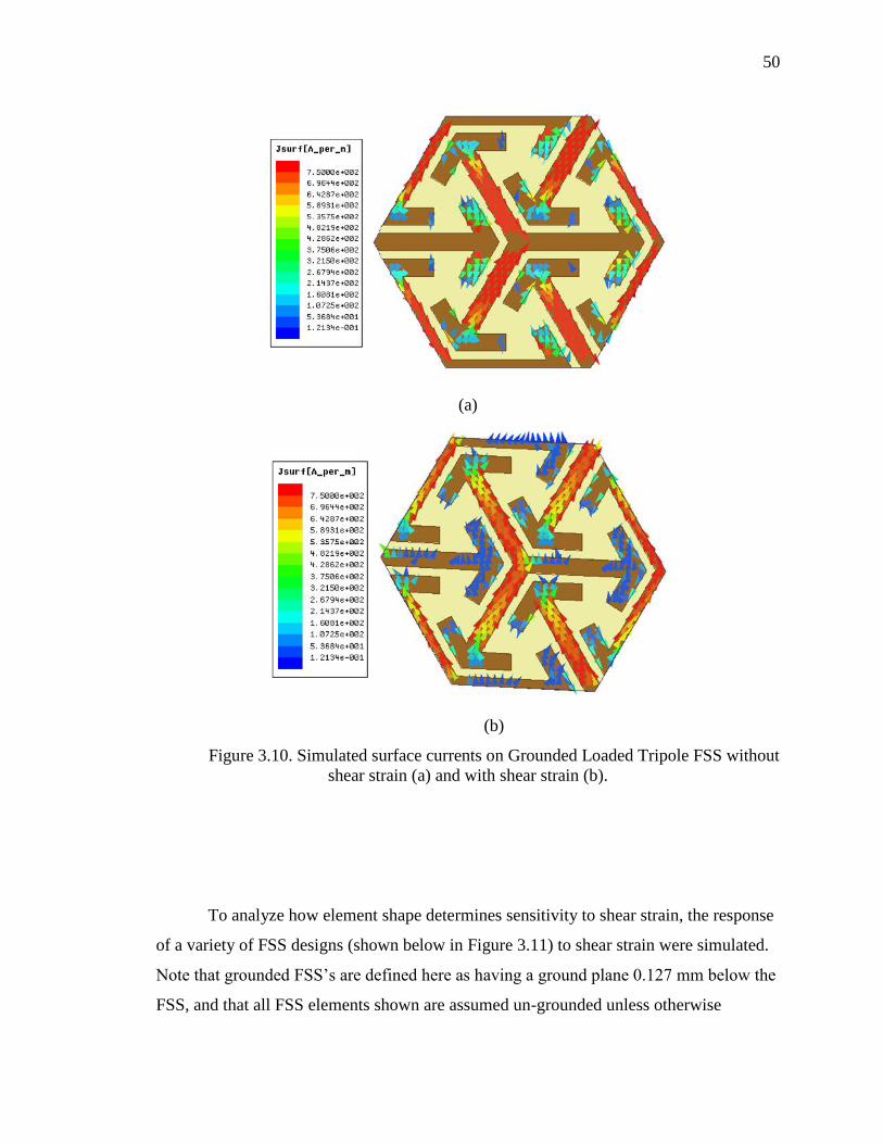
50
(a)
(b)
Figure 3.10. Simulated surface currents on Grounded Loaded Tripole FSS without
shear strain (a) and with shear strain (b).
To analyze how element shape determines sensitivity to shear strain, the response
of a variety of FSS designs (shown below in Figure 3.11) to shear strain were simulated.
Note that grounded FSS’s are defined here as having a ground plane 0.127 mm below the
FSS, and that all FSS elements shown are assumed un-grounded unless otherwise

51
specified. Since the magnitude of the cross-polarization peak doesn’t change linearly
with shear strain, a single shear modulus cannot be determined (as was done above for
normal strain in Equation 3.1). Instead, the magnitude of cross-polarization for each
element is shown as a function of shear strain (Sxy) in Figure 3.12. Specifically, each
cross-polarization magnitude response is taken from the maximum cross-polarization
response for each element. This generally occurs at or near the co-polar resonant
frequency of the FSS, meaning that in practical applications, only this frequency will
have to be measured.
Overall, it appears that grounded FSS elements generally have a stronger cross-
polarization response than the equivalent ungrounded FSS designs, even when un-
deformed. This behavior can act as both a benefit and a drawback, depending on the
desired sensing requirements. On one hand, this higher cross-polarization level (>-20
dB) makes it relatively easy to detect in measurement, which may be a concern for
practical implementations of FSS sensors in high loss or electrically noisy environments.
Additionally, higher cross-polarization levels can allow simpler and more affordable
measurement equipment to be used, rather than a VNA. On the other hand, by having a
higher baseline of cross-polarization (i.e. zero shear strain response), the cross-
polarization caused by shear strain quickly reaches its highest limit, as was seen for the
grounded loaded tripole FSS. While this can be useful for detection of shear strain, it
limits the ability of the FSS to characterize the shear strain through cross-polarization
magnitude measurements alone. As such, the bandwidth (defined as the range of
frequencies between the points that are -3dB from the peak) of the cross-polarized
resonant peak will also be needed for characterization of larger shear strains.
Furthermore, it may not always be practical to implement a conductive sheet in a
structure to act as a ground plane for an associated FSS (particularly for embedded
sensing applications). As such, development of a non-grounded FSS element that gives
high cross-polarization levels when un-shear strained (without reaching the observed
maximum limit too quickly) would be beneficial. Of the elements observed, the element
that best fits these criteria is the loaded cross-loop design, shown in Figure 3.11. The co-
polarized and cross-polarized responses of this element are displayed in Figure 3.13 (a)
and (b), respectively.

52
Crossed-Dipole FSS Jerusalem Cross FSS Cross-Loop FSS Loaded Cross-Loop FSS
Square Loop FSS Tripole FSS Loaded Tripole (Grounded and Ungrounded) (Grounded and Ungrounded)
Figure 3.11. FSS elements investigated in Figure 3.12.
Figure 3.12. Simulated reflection response magnitude of cross-polarization plotted as a
function of shear strain for FSS elements of Figure 3.11.

53
(a)
(b)
Figure 3.13. Simulated Co-polarized (a) and cross-polarized (b) frequency
response for a Loaded Cross Loop FSS under shear strain.

54
Based on the results of Figure. 3.13, a number of advantages are observed. First,
unlike the ground-backed loaded tripole FSS design response seen in Figure 3.9, the
loaded cross loop FSS has a co-polarized reflection response that is essentially
unaffected by shear strain. This means that the effects of normal strain and shear strain
can be easily distinguished for this FSS, allowing this FSS to be used to sense both
deformations simultaneously. Second, this FSS design has a higher cross-polarization
level for shear strain than other, non-grounded FSS designs, and is comparable to cross-
polarization levels seen for the grounded FSS designs investigated. As such, after ~0.01
shear strain, this peak will be relatively easy to detect in a practical measurement (in
which electrical noise or environmental reflections might obscure the FSS response),
while also not requiring the presence of a ground plane. As a result, the loaded cross-
loop FSS appears to be an excellent candidate for normal strain and shear strain sensing
purposes.
3.3. APPLICATION OF FSS FOR STRAIN/SHEAR/BUCKLING DETECTION IN
STEEL-TUBE REINFORCED CONCRETE COLUMNS
Thus far, all investigations into the response of FSS to deformations have either
been through simulation or controlled lab experiment. To further extend the work,
measurements were conducted using a grounded crossed-dipole and square loop FSS that
were embedded into a set of steel-tube reinforced concrete columns. These elements
were chosen for their straightforward design principles, ease of in-house production,
angle insensitivity, and for their strong SHM performance, as shown in the previous
sections. Meanwhile, the columns used in this test represent a novel advancement in
concrete support structures, and take the form of a hollow, steel-tube core, around which
the concrete column is poured [38]. This hollow-steel core acts to reinforce the concrete
column, giving it structural stability that is comparable to a solid concrete column, but
with reduced weight. Additionally, a fiber-reinforced plastic (FRP) layer surrounds the
concrete column, acting as a casing during the pouring of the concrete column, as well as
providing a layer of protection from environmental exposure [38]. A cross sectional view
of the column structure is shown in Figure 3.14.

55
Steel-tube
Concrete
FRP Wrap
16" 4" 0.375"
Figure 3.14. Cross-section of concrete column.
To validate the structural integrity of these columns, two structural loading tests
were conducted; a lateral displacement test and a torsion test. The lateral displacement
test consisted of a vertically oriented concrete column that underwent horizontal
displacement at the top of the column. This displacement caused the steel-tube core of
the column to undergo significant vertical normal strains (and resultant buckling when
the column failed mechanically) due to interactions between the column and the static
concrete footing that acts as the column base [38]. Here, buckling is defined as a severe
bending of the steel-core due to compressive normal strain. This buckling can weaken
the steel, and can thus lead to possible structure failure if not detected. An illustration of
the lateral displacement test is shown in Figure 3.15.
The most significant normal strains and subsequent buckling occur near the
bottom of the steel-tube core, at the interface between the column and the footing, and
located in the direction of lateral displacement. As such, the base of the steel-tube was
chosen as the location to apply the FSS sensor, which for this test was the grounded

56
square loop FSS, which was found in simulation to be the more sensitive of the two FSSs
to normal strain. Meanwhile, the torsion test consisted of a vertical concrete column that
underwent a twisting force at the top of the column. This twisting force was applied
using two linear actuators moving in opposite directions on either side of the column.
This twisting caused shear strain to occur along the base of the column due to interactions
between the twisted column and static footing. By applying an FSS to the steel column
in this region, shear strain can deform the FSS, causing the FSS to cross-polarize incident
radiation. The grounded crossed-dipole FSS was chosen for this test, as simulation
showed that it was more sensitive to shear strain than the grounded square-loop FSS.
Concrete
Column
Buckling
Displacement
Figure 3.15. Diagram of linear displacement test.

57
For the purposes of embedding FSS sensors into the above concrete columns, a
number of practical considerations had to be made in the FSS design process. Such
considerations included the effects of conforming the FSS to the column’s curvature, as
well as compensation for the effects of loss and internal reflections that occurred within
the geometry of the column. The effects of curvature were accounted for by choosing
FSS elements that are insensitive to incident angle, with this insensitivity verified by
simulation of a curved FSS. As for material considerations, radiation at microwave
frequencies experiences significant power loss in concrete due to the concrete’s water
content (i.e. dielectric loss), making it difficult for interrogating signals to penetrate
through the concrete. Additionally, course aggregates in the concrete can cause
unintended scattering of incident signal. This results in a reduction in power reflected
from the FSS, making these resonances harder to detect. This loss was partially
accounted for by designing the FSSs to operate in the S-band (2.6-3.95 GHz), as lower
frequencies experience less dielectric loss. Signal reflections within the concrete
structure were another concern, as the thickness of the concrete layer was comparable to
the wavelength of the interrogating signal. The combined reflections from dielectric
boundaries in a layered structure can lead to alterations in the structure’s frequency
response, such as the creation of resonances based on the thickness of the dielectric
layers. As such, the concrete structure may have (inherent) resonant behavior that would
mask the FSS resonance [54]. In order to reduce these reflections, a pair of dielectric-
filled horn antennas were designed and built for interrogation of the concrete columns.
By using a dielectric-filled horn, the impedance of the horn would better match the
concrete column, reducing reflections and increasing the power incident on the FSS.
Additionally, the apertures of these horns were curved to conform directly onto the
columns, as an air gap would be otherwise present for a flat aperture. These horns were
manufactured by 3-D printing a dielectric material (εr = ~ 3, and nominal loss factor) into
the shape of the desired horn and wrapping the dielectric in conductive tape. A
photograph of one of the horn antennas is shown in Figure 3.16.

58
Figure 3.16. Filled horn antenna for measuring FSS embedded in concrete
column.
The grounded crossed-dipole and grounded square loop FSS designs used for this
investigation were simulated before being built and tested in the lab. Both FSSs were
etched onto a thin film of conductor backed Roger’s 3006 PCB material having a
thickness of 0.25 mm, εr of 6.15, and the loss tangent of 0.0015. The frequency response
of each sample was measured when flat and when conformed over a curved surface
(similar to that of the column) to ensure that the curvature does not adversely affect the
FSS’s frequency response. Images of the completed grounded crossed-dipole and
grounded square loop FSS samples are shown in Figure 3.17 (a) and (b), respectively.
Additionally, the measured reflection responses for both the cross FSS and square loop
FSS are given in Figure 3.18 (a) and (b), respectively, for both flat and curved contours.

59
(a)
(b)
Figure 3.17. Grounded crossed-dipole FSS (a) and grounded square loop FSS (b)
samples.

60
(a)
(b)
Figure 3.18. Reflection responses of grounded cross FSS (a) and grounded square
loop FSS (b) in planar and curved states.

61
From the results shown in Figure 3.18, the FSSs were found to have
distinguishable resonances at 3.248 GHz (for the grounded crossed-dipole FSS) and
3.174 GHz (for the grounded square loop FSS). Once constructed, the FSS samples were
attached to the steel-tube cores of the test columns. The method of attaching the FSS
samples was of critical importance, as a poor adhesion could have lead to detachment
during deformation. Furthermore, depending on how the FSS was adhered to the
structure, deformations on the steel-core potentially may not translate completely to the
FSS, thus reducing the sensitivity and effectiveness of the FSS for normal/shear strain
sensing. For the purposes of this test, the FSS samples were adhered to the steel-core
using 3M Hi-Strength 90 Spray Adhesive. This adhesive was chosen for its high strength
and large surface-area applicability. The locations of the FSS samples applied to the
steel-tube cores are shown in Figure 3.19.
Figure 3.19. FSS samples applied to steel-tube cores.

62
For each measurement setup, the dielectric-filled horns were attached to the
concrete columns over the locations of the FSS samples. For the lateral displacement test
(grounded square-loop FSS sensor), the two horns were oriented to provide a co-
polarized frequency response between the horns, as this test was intended to measure
normal strain in the FSS. Conversely, for the torsion test (crossed-dipole FSS sensor),
the horns were oriented to provide a cross-polarized frequency response to measure shear
strain in the embedded FSS. In each test, an external 30 dB amplifier was added to the
transmitting port to amplify the interrogating signal to counteract losses (mentioned
above) in the concrete column. This system was measured using at S-band (2.6-3.95
GHz) using a calibrated Agilent 8753 VNA.
During the lateral displacement test, the top of the column was displaced
positively and negatively, relative to the hydraulic actuator that applied the displacement.
This displacement deformed the FSS with both negative (compression) and positive
(tension) normal strain. Displacements were applied gradually (in cycles) over the course
of the test, in such a way so that the actuator applied increasing displacement with each
cycle. During each cycle, the column was positively displaced by a certain amount, and
then negatively displaced by the same amount. This was repeated twice for each
displacement. The total displacement ranged from 0.05 inches for the first cycles to 15.3
inches of displacement in the final cycles. Measurements of the FSS response were
conducted at the positive and negative apexes (maximums) of displacement for the first
repetition of each cycle. By observing the difference in resonant frequency between the
strained and un-strained FSS for each displacement, the associated strain could be found
by dividing the frequency difference by the gauge factor of the FSS (calculated by
Equation 3.1 as
[35]. The value of ς for the grounded square loop FSS used in
this test was determined through simulation to be 0.43. Based on this value, the
measured normal strain for the first cycle of each displacement is shown in Figure 3.20.
For negative displacement, normal strain is relatively small until approximately -3
inches of displacement, at which point the normal strain magnitude increases with
displacement magnitude before reaching a plateau at about 0.05 normal strain. Similar
behavior is seen for positive displacement, with significant normal strain only occurring
after about 6 inches of displacement. After this point, the magnitude of normal strain

63
increases linearly with displacement until it reaches a value of approximately -0.025 at 13
inches of displacement. These normal strain values are compared to those measured by
traditional strain gauges in Figure 3.21 as a verification of the FSS’s performance. Two
sets of strain gauge data are plotted, corresponding to data taken at the apexes of the two
cycles for each displacement. The strain gauge measurements are only reported for
displacements between -4 to 4 inches, due to limitations in the strain gauges.
Figure 3.20. Normal strain measured from FSS as a function of displacement.
Figure 3.21. Comparison of normal strain data from FSS and strain gauge sensors.

64
Overall, there is good agreement between the FSS and strain gauge, with minor
aberrations in the FSS data set occurring for displacements around zero. These
aberrations may be a result of the measurement not taking place at exactly at the apex of
each displacement cycle due to the non-instantaneous measurement time of the VNA, as
well as human error in timing the measurement with the apex of the strain cycle. This
would have the most significant effect for small displacement cycles, as these cycles
occurred more quickly in the testing process than the larger displacement cycles.
Additionally, for the larger displacement values, normal strains measured by the FSS are
larger in magnitude than those measured by the strain gauges. This may be due to the
simulated gauge factor not exactly matching that of the physical FSS sample. A similar
behavior was observed for the FSS measurements shown in Figure 3.6 of Section 3.1,
which could indicate that a more reliable gauge factor determination method may be
needed that takes the effects of Poisson’s Ratio into account.
For the torsion test, a testing procedure similar to the linear displacement test was
conducted. In this test, torsion was applied to the column through a set of linear actuators
connected to the top of the column. Torsion was applied in cycles, with the column first
being twisted clockwise and then counter-clockwise for each cycle. Furthermore, the
magnitude of this twisting increased with each additional cycle. Measurements of the
cross-polarized FSS response were taken at the apex of each cycle, with the goal of
detecting increases in cross-polarization due to torsion-applied shear strain of the FSS.
Unfortunately, however, no change was detected in the cross-polarized response over the
course of the test. This may indicate that shear strain was not applied to the FSS as
expected, meaning that cross-polarization would not have occurred. This could be due to
the column not deforming as expected, or due to shear strain not correctly transferring to
the FSS. Alternatively, the returning signal may have been below the noise floor
(~ -70dB) of the VNA. In either case, the ability of an FSS to detect shear strain was not
verified in this investigation, and therefore requires additional investigations including
improved test and measurement procedures.

65
3.4. CONCLUSION
Over the course of this section, the use of FSS for detecting deformations in a
structure was discussed. In Section 3.1 and 3.2, the effects of normal strain and shear
strain on the frequency response of an FSS were examined through both simulation and
measurement of deformed FSS samples. In Section 3.1, it was found that the resonant
frequency of an FSS shifts when under normal strain due to normal strain changing the
length of the FSS element and altering the resonant wavelength. Additionally, it was
shown that this resonant shift was also a function of the polarization of the interrogating
wave with respect to the direction of normal strain. Specifically, the effect of normal
strain on resonant frequency was greatest when the incident wave polarization and
normal strain direction were parallel. Based on these observations, FSSs were shown to
have potential to sense both normal strain magnitude and normal strain direction. To
verify these observations, an FSS sample that had been subjected to normal strain was
measured for different polarizations. Although overall trends matched expectations
(resonant frequency shifting as a function of normal strain), the magnitude of this shift
was less than was seen through simulation. Additionally, for incident wave polarizations
oriented normal to the direction of normal strain, resonant frequency shifts were greater
than expected. Ultimately, these results indicate potential limitations for normal strain
sensing (possibly due to the effects of Poisson’s Ratio) that may require future
investigations, as well as the need for a secondary method of measuring normal strain
such as commercial strain gauges for comparison.
For the case of shear strain in Section 3.2, simulations indicated that shear strain
causes an FSS to cross-polarize incident radiation due to the FSS losing geometrical
symmetry. The magnitude of this cross-polarization was found to increase with shear
strain, resulting in a potential method for detecting shear strain. The sensitivity of a
number of FSS elements to shear strain was analyzed for sensing purposes. This study
indicated that while grounded FSS designs caused the highest level of cross-polarization
for a given shear strain, the cross-polarization would quickly reach an observed
maximum value, meaning that cross-polarization magnitude would cease to increase for
higher shear strains. Of the non-grounded elements, the loaded cross-loop FSS was
found to provide the most sensitive response to shear strain, giving the highest magnitude

66
of cross-polarization of the non-grounded elements examined while also avoiding a
maximum limit for the simulated shear strain values. Unfortunately, for the case of shear
strain, laboratory measurements were not conducted due to the difficulty in applying
shear strain to the available FSS sample. As such, future work will need to be undertaken
to conduct such a measurements, thus providing validation of simulated results.
Finally, in Section 3.3, FSS samples were embedded into a set of concrete
columns to act as normal strain and shear strain sensors during lateral displacement and
torsion tests of these columns. This project provided examples of difficulties that might
be encountered for FSS sensing in practical structures. For the structures used in this
project, one such difficulty regarded the high signal loss of the concrete, as this loss
heavily dampened the interrogating signal, making detection of the FSS problematic.
This loss was counteracted by using an amplifier on the interrogating signal, as well as
reducing the noise floor of the VNA used during measurement (at the cost of longer
acquisition times). Another difficulty was due to the thickness of the concrete columns
causing additional resonances in the measured frequency response due to reflections at
dielectric interfaces within the layered dielectric structure of the column, masking the
resonance of the FSS. This was (partially) counteracted by using dielectric-filled horn
antennas to measure the FSS, as these horns would reduce reflections by matching the
impedance of the columns. Finally, the curvature of the columns meant that the FSS
samples used for this project had to be designed with such curvature in mind. For the
lateral displacement test, a shift in resonant frequency was observed for applied normal
strain, as expected from results found in Section 3.1. Furthermore, the normal strain
measured by the FSS matched well with traditional strain gauges that were also
embedded in the column. However, for the torsion tests, no cross-polarization was
detected for over the course of the test. This may have been due to shear strain not being
applied to the FSS, or due to shear strains not causing the FSS to cross-polarize incident
radiation as expected. As such, future work will need to include additional investigations
into the effects of shear strain on FSS samples, likely under more controlled
circumstances to ensure that the FSS samples have shear strain applied as expected.
67
4. APPLICATIONS OF FSS FOR DELAMINATION/DISBOND SENSING
In Section 3, it was shown that geometrical deformation of an FSS affects the
FSS’s frequency response. Conversely, by (remotely) monitoring the FSS’s frequency
response, the presence of a deformation may be determined. Further, as discussed in
Section 2, an FSS’s frequency response is also affected by materials (e.g., dielectrics)
surrounding the FSS, providing another potential sensing application. In this section, this
material dependency is utilized for detection of separations (i.e., delaminations and
disbonds) between layers of a layered dielectric structure.
4.1. FSS RESPONSE TO DELAMINATION WITHIN A STRUCTURE
The formation of delaminations and disbonds in a layered dielectric structure may
lead to structural failure, giving rise to the need for delamination/disbond detection. A
delamination is defined as a separation that occurs in a laminated material, such as a
composite structure [43]. Alternatively, a disbond is defined as a form of delamination
composed of a separation between two separate materials that had previously been
bonded together. In either case, this separation creates an air gap in the structure that can
lead to structural failure. Therefore, the ability to sense the presence of
delaminations/disbonds is critical for assessing structural integrity. Current
delamination/disbond sensing techniques include ultrasound [42], thermography [40], and
microwave interrogation [41]. In addition to these methods, FSSs may also be used for
delamination/disbond detection by taking advantage of their sensitivity to dielectric
materials in the vicinity of the FSS [54].
As discussed in Section 2.2, the frequency response of an FSS is sensitive to the
presence of surrounding materials including (mechanically supportive) dielectric
substrate layers. This occurs due to the dielectric material altering the capacitive
coupling that occurs between elements of the FSS, thus changing the FSS’s resonant
frequency. Normally, when integrating an FSS into a layered dielectric structure, the
design of the FSS (element spacing, etc.) must be adjusted to account for this additional
capacitance. Thus, the FSS is “tuned” to provide a specific response for a particular
dielectric structure. However, should the dielectric structure change due to the presence

68
of a delamination in the structure, the FSS capacitance will be reduced. When this
occurs, the resonant response of the FSS is changed as well.
4.1.1. Simulation Results. To investigate how the FSS resonance is affected by
delamination, a full-wave simulation in HFSS [23] was conducted for a crossed-dipole
FSS embedded between two planar dielectric sheets having a permittivity of 3.3, loss
tangent of 0.004, and thickness, t, of 1.524 mm. The delaminated structure and
embedded crossed-dipole FSS used for this simulation are shown in Figure. 4.1 (a) and
(b), respectively. Meanwhile, the resultant frequency response for three different
delamination distances are shown in Figure. 4.2.
L=17mm
g=4.5mm
w=5mm
t Superstrate
Delamination
Distance
t Substrate
FSSAir
(a) (b)
Figure 4.1. Crossed-dipole FSS (a) embedded into a delaminated structure (b).
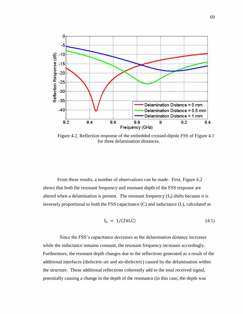
69
Figure 4.2. Reflection response of the embedded crossed-dipole FSS of Figure 4.1
for three delamination distances.
From these results, a number of observations can be made. First, Figure 4.2
shows that both the resonant frequency and resonant depth of the FSS response are
altered when a delamination is present. The resonant frequency (f0) shifts because it is
inversely proportional to both the FSS capacitance (C) and inductance (L), calculated as
(4.1)
Since the FSS’s capacitance decreases as the delamination distance increases
while the inductance remains constant, the resonant frequency increases accordingly.
Furthermore, the resonant depth changes due to the reflections generated as a result of the
additional interfaces (dielectric-air and air-dielectric) caused by the delamination within
the structure. These additional reflections coherently add to the total received signal,
potentially causing a change in the depth of the resonance (in this case, the depth was

70
reduced). As such, by monitoring both parameters, one can acquire two sets of data from
which delamination information (such as severity and location) may be obtained.
Additionally, the sensitivity of both resonant frequency and resonant depth to
delamination can help differentiate the effects of delamination from other structural
deformations of sensing interest, such as normal strain, which only affects resonant
frequency. In other words, in a system where both normal strain and delamination may
occur, a significant change in both resonant frequency and depth may indicate the
presence of delamination, whereas observing only a shift in resonant frequency may be
indicative of normal strain alone. As a result, a single FSS can conceivably be used to
separately detect both normal strain and delamination (as well as shear strain, potentially,
since shear strain doesn't typically affect the co-polarized frequency response, as
discussed in Section 3.2). This gives a single FSS the potential to act as a comprehensive
distributed structural health monitoring sensor. One limitation with this method is that it
may be difficult to separately quantify normal strain and delamination if both are present.
However, the presence of a delamination can often be considered a major structural
failure [43]. As such, normal strain assessment may no longer be important in this case,
since the structure has already reached a critical failure state due to the delamination.
That being said, by better characterizing how delaminations affect an FSS’s frequency
response, it may still be possible to separately quantify these two phenomena. To this
end, the resonant frequency and resonant depth of the FSS-integrated layered structure
from Figure 4.1 are shown as a function of delamination distance in Figure 4.3 (a) and
(b), respectively.
From Figure 4.3, it is seen that for thin delaminations (less than 2 mm), the
resonant frequency monotonically increases as the delamination distance increases.
Additionally, for very thin delaminations (less than 0.2 mm), the increase in resonant
frequency occurs more rapidly than for the slightly larger delaminations (0.3 mm - 2
mm). This is because the capacitive electric field coupling of the FSS is concentrated
close to the FSS surface. As such, changes in a dielectric that occur farther from an FSS
have less of an effect on the resonance, since less of the electric field coupling is present
in that region. This behavior is further discussed later in this section.

71
(a)
(b)
Figure 4.3. Resonant frequency (a) and resonant depth (b) of the embedded
crossed-dipole FSS shown in Figure. 4.1 as a function of delamination distance.
The results of Figure 4.3 (b) show a similar trend for the relationship between
resonant depth and thin delaminations. For instance, when a delamination is very thin

72
(less than 0.1 mm) the resonance becomes slightly deeper. This is likely due to the newly
formed air gap changing the overall structure (effective) impedance to be closer to that of
the surrounding environment (in this case, free space) and therefore reducing reflections
at the resonant frequency. Next, as the delamination distance increases, the resonance
becomes heavily dampened due to additional reflections in the structure (introduced by
the new interfaces created by the delamination), with the reflection resonance becoming
most shallow at ~2.5 mm of delamination. For the 2 mm - 5 mm delamination range,
however, the trends in resonant frequency and depth become reversed. After reaching a
peak value in resonant frequency of 11.5 GHz at 3 mm of delamination, the resonant
frequency reduces to 11 GHz at 5 mm of delamination. Additionally, the observed
reflection resonance quickly deepens again at 3.5 mm of delamination, reaching a depth
of -50 dB, before eventually returning to a shallower level as delamination distance
continues to become larger. This is likely due to a resonant frequency (inherent to the
delaminated dielectric structure) that is near the resonant frequency of the FSS. To
illustrate this, the resonant frequencies of the dielectric structure itself (without an
embedded FSS) are shown with respect to delamination distance in Figure 4.4.
Figure 4.4. First three resonances of dielectric structure given in Figure 4.1 (b) as
a function of delamination distance.
73
From the results of Figure 4.4, it can be seen that at approximately 2.5 mm of
delamination, the first resonance of the dielectric structure begins to approach the
resonance of the FSS. Since the FSS resonance is most shallow at this point, the
dielectric resonance dominates the overall reflection response. Qualitatively speaking,
since the dielectric resonance is stronger, the overall resonant frequency is weighted by
this resonance. Furthermore, the deeper resonance for 2.5 mm of delamination in Figure
4.3 (b) occurs approximately where the dielectric resonance overlaps the overall
resonance, causing the resonance to reach its deepest point. However, as the structure’s
resonance continues to decrease in frequency for increasing delamination, the structural
and FSS resonances no longer overlap. As such, the overall resonance is dampened again
as the delamination distance continues to increase.
Another aspect to consider is the influence of delamination location on the FSS
response. Thus far, the delaminations have occurred at the interface of the FSS. Since an
FSS is more sensitive to dielectric changes that occur locally, delaminations occurring at
other locations within a structure may have a reduced effect on the FSS response. To
investigate this, full-wave simulations were conducted for the structures shown in Figure
4.5 (a) and (b), referred to as the “Near” delamination case (at the location of the FSS)
and “Adjacent to” delamination case (at the next dielectric interface (1.524 mm) from the
FSS), respectively. The FSS design used here is identical to the FSS in Figure 4.1 (a).
Additionally, the dielectric layers used have the same parameters as those found in Figure
4.1 (b).
The resonant frequency and resonant depth of the FSS as a function of
delamination distance are shown in Figure 4.6 (a) and (b), respectively, for the "Near"
and "Adjacent to" delamination cases. Additionally, the resonant frequency of the
standalone dielectric structure (without an embedded FSS being present) is also included
in Figure 4.6 (a).

74
Delamination
DistanceAir FSS
Substrate1
Substrate2
2t
Delamination
DistanceAir
FSSt Superstrate
t Substrate1
t Substrate2
(a) (b)
Figure 4.5. Dielectric structures for “Near” delamination (a) and “Adjacent to”
delamination (b) cases.
(a)
Figure 4.6. Resonant frequency (a) and resonant depth (b) of the crossed-dipole
FSS in Figure 4.1 as a function of delamination distance for the “Near” and “Adjacent to”
delamination cases illustrated in Figure 4.5.

75
(b)
Figure 4.6. Resonant frequency (a) and resonant depth (b) of the crossed-dipole
FSS in Figure 4.1 as a function of delamination distance for the “Near” and “Adjacent to”
delamination cases illustrated in Figure 4.5. (cont.)
Overall, similar trends to what was seen in Figure 4.3 (in regards to a
delamination occurring at the FSS location, albeit in different dielectric structures) are
also seen here in Figure 4.6, with the FSS resonance initially dampening while shifting
upward in frequency, before eventually interacting with the resonance of the delaminated
dielectric structure (red line in Figure 4.6). However, the resonant frequency is less
affected for the “Adjacent to” case than for the “Near” delamination case. This is
attributed to the “Adjacent to” delamination case having less of an effect on the FSS’s
capacitance than the “Near” delamination case, since capacitive coupling occurs close to
the FSS. Additionally, since the resonant frequency doesn't shift as much for the
“Adjacent to” case as for the “Near” case, a thicker delamination (and thus lower
resonant frequency for the dielectric structure) is required before the dielectric structure
and FSS resonances overlap and interact, which occurs for this case at approximately 3
mm of delamination.

76
For delamination sensing purposes, these observations imply that a single FSS
may only be able to sense delaminations within its local area. Delaminations occurring
farther away have a reduced impact on the frequency response of the FSS. For larger
dielectric structures, this may be a problem, as a single FSS may not be able to
adequately monitor the entire structure. As such, the use of multiple FSSs embedded
throughout the structure may be required for complete sensing coverage. However, in
order to include multiple FSS layers in a structure, a number of design considerations
must be included [30]. First, to differentiate the resonances of the different FSS layers,
the resonant frequencies of each layer must be spaced far enough apart in frequency to
avoid unwanted interactions between resonances. As a result, the response of each
individual FSS can be separately monitored. Conversely, however, the resonances must
be close enough together to all fit within the operating frequency band (potentially
requiring a wideband interrogation system). As a result, there may be a limit to how
many resonances can be used to monitor a structure. Finally, the spacing between FSS
layers in the structure must be carefully chosen. For instance, if the FSS layers are
spaced too far apart, there may be “blind spots” in the dielectric structure where a
delamination won't be detected due to its distance from the FSS layers. Alternatively, if
the FSS layers are too close together, the layers may electrically couple and affect/change
their intended response [30].
With the above observations in mind, a full-wave simulation was conducted to
investigate how multiple FSSs embedded within a dielectric structure respond to
delaminations occurring between different layers of the structure. For this investigation,
two FSSs were embedded in the structures shown in Figure 4.8 (a-e), where each
structure represents a different delamination location (referred to as Delams 1-5). The
crossed-dipole FSS shown in Figure 4.1 was used for the first FSS layer, while the cross-
loop FSS design shown in Figure 4.7 was used for the second FSS layer. The
transmission response resonant frequencies for each FSS are given in Figure 4.9 for each
delamination as a function of delamination distance. The transmission response was
considered here in order to take advantage of the two transmission resonances of the
cross-loop FSS. The lowest and highest resonant frequencies, 3.6 GHz and 8.5 GHz for
no delamination (delamination distance of zero in Figure 4.9) correspond to the cross-

77
loop FSS, while the middle resonance, 6 GHz for no delamination, corresponds to the
crossed-dipole FSS. Meanwhile, the transmission response resonant depths of each FSS
resonance are given in Figure 4.10 as a function of delamination distance for each
delamination scenario of Figure 4.8.
1mm
3mm
14mm6mm
Figure 4.7. Cross Loop FSS used in multi-layer FSS structure for delamination
analysis in Figure 4.8.
1.524mm
Delamination
Distance
1.524mm
1.524mm
1.524mm
1.524mm
Delamination
Distance
1.524mm
1.524mm
1.524mm
1.524mm
Delamination
Distance
1.524mm
1.524mm
1.524mm
1.524mm
Delamination
Distance
1.524mm
1.524mm
1.524mm
1.524mm
Delamination
Distance
1.524mm
1.524mm
1.524mm
Cross FSS
Cross Loop FSS
εr = 1
εr = 3.3
εr = 3.3
εr = 3.3
εr = 3.3
Cross FSS
Cross Loop FSS
εr = 1
εr = 3.3
εr = 3.3
εr = 3.3
εr = 3.3
Cross FSS
Cross Loop FSS
εr = 1
εr = 3.3
εr = 3.3
εr = 3.3
εr = 3.3
Cross FSS
Cross Loop FSSεr = 1
εr = 3.3
εr = 3.3
εr = 3.3
εr = 3.3
Cross FSS
Cross Loop FSSεr = 1
εr = 3.3
εr = 3.3
εr = 3.3
εr = 3.3
(a) (b) (c)
(d) (e)
Delam 1 Delam 2 Delam 3
Delam 4 Delam 5
Figure 4.8. Simulated delaminated dielectric structures, referred to as Delams 1-5.

78
Figure 4.9. Simulated resonant frequencies as a function of delamination distance
for Delams 1-5 shown in Figure 4.8. The top and bottom resonances correspond to the
cross-loop FSS, while the middle resonance corresponds to the crossed-dipole FSS.

79
(a)
(b)
(c)
Figure 4.10. Simulated values of resonant depth as a function of delamination
distance for Delams 1-5 (Figure 4.8). (a) and (c) correspond to the cross-loop FSS and
(b) corresponds to the crossed-dipole FSS

80
Based on these simulations, Delams 1-5 affect each FSS resonance differently.
For Delam 1 in Figure 4.8 (a), the resonance of the crossed-dipole FSS shifts by about 1
GHz, while the resonances of the cross-loop FSS are less affected, shifting by less than
0.1 GHz. This behavior verifies that an FSS is only sensitive to local delaminations, as
only the crossed-dipole FSS resonance is significantly affected by Delam 1. The crossed-
dipole FSS resonance also shifts in resonant frequency for Delam 2 (shown in Figure 4.8
(b)), shifting by 1.6 GHz over the delamination distance observed. This shift in resonant
frequency is greater than what was seen for Delam 1, despite both delaminations being in
the same proximity to the crossed-dipole FSS. This increase in delamination sensitivity
is also observed in the second resonance of the cross-loop FSS, which exhibits a much
larger frequency shift than was seen for Delam 1. This increase in sensitivity for both
resonances may be due to additional electric field coupling between the FSS structures
that is weakened by the presence of the delamination, reducing the capacitance of both
FSSs. Furthermore, the crossed-dipole and second cross-loop FSS resonances begin to
overlap after 3.5 mm of delamination distance, creating a single resonance. For practical
purposes, such an overlap may be undesirable, as this makes it difficult to independently
track the resonance of each FSS. However, 3.5 mm of delamination would likely have
already caused the structure to fail, meaning that delamination sensing would no longer
be a concern. As such, knowing the maximum required delamination distance for a given
structure is important when choosing the multi-layer FSSs’ resonance spacing in the
overall frequency response. Additionally, this combination of resonances causes a
substantial increase in resonant depth at 3.5 mm of delamination distance, before
subsequently reducing as the delamination continues to widen. For all other
delaminations, the resonant depth does not include the erratic changes seen for Delam 2,
as these delamination cases don’t cause resonance overlap. For Delam 3, shown in
Figure 4.8 (c), all three resonances exhibit a similar frequency shift. This similarity in
frequency shift between resonances occurs because Delam 3 is spaced directly between
the two FSS layers, thereby affecting each FSS in a similar way. Next, for Delam 4 in
Figure 4.8 (d), the cross-loop FSS resonances are each altered by ~1.5 GHz over the
observed delamination distances, while the crossed-dipole FSS resonance is largely
unaffected. Much like the resonant responses to Delam 1 and Delam 2, this behavior is a

81
result of the close proximity of Delam 4 to the cross-loop FSS, again demonstrating the
local sensitivity of an FSS to delamination. Lastly, similar behavior is also seen for
Delam 5 in Figure 4.8 (e), albeit with less shifting in the cross-loop resonances. This
behavior mirrors the difference in delamination response seen between Figure 4.8 (a) and
(b), where the delaminations occurring between the two FSS layers cause a more
significant impact on the frequency response than delaminations occurring between the
FSSs and the outermost dielectric layers. One final observation is that unlike for the
reflection response in Figure 4.4, the transmission response doesn’t feature a dielectric
structure resonance. A selection of transmission responses for the delaminated structures
of Figure 4.8 (without FSSs) are shown in Figure 4.11.
Figure 4.11. Transmission responses for the structures shown in Figure 4.8,
without embedded FSSs.

82
As Figure 4.11 indicates, the transmission responses for the delaminated
structures in Figure 4.8 don’t vary significantly over the observed frequency spectrum,
(the largest variation is less than 4 dB for the 5 mm Delam 3 case). As a result, instead of
being altered by structural resonances, the resonant depths of each FSS resonance change
smoothly with delamination distance, as seen in Figure 4.3 (b). This is beneficial from a
sensing point-of-view, as the presence of a delamination is the only aspect that causes a
change in resonant response. Additionally, measuring the transmission response may
prove advantageous should structural resonances mask the FSS resonances in the
reflection response. However, transmission measurements may be impractical in some
real world sensing cases, as both sides of a structure (required for transmission
measurements) may be inaccessible. Overall, based on these preliminary results, the use
of multiple FSS layers for delamination detection appears quite promising, as this method
can provide remote, non-contact delamination monitoring for an entire structure, while
also providing information on delamination location.
4.1.2. Measurement Results. To verify the ability of embedded FSSs to detect
the presence of delaminations, a series of measurements were conducted on layered
dielectric samples with embedded FSSs. The FSSs used for these measurements were the
crossed-dipole FSS shown in Figure 4.1, and the cross-loop FSS shown in Figure 4.7.
These samples were constructed through chemical etching of 8”x11” copper-clad Rogers
RO4053 PCB boards (1.524 mm thick, permittivity of 3.3 and loss tangent of 0.004), as
was used in simulation. Although these FSS samples are not infinite in extent (as is
assumed in simulation), all but the outermost FSS elements will contribute to an FSS
response that is similar to the ideal (infinite dimensions) case, as most coupling only
occurs with directly adjacent elements. Furthermore, the size of the FSS sample was
larger than the interrogating beam, thus avoiding significant edge effects. The copper
cladding was removed from two additional Rogers RO4053 boards to serve as additional
dielectric layers. The FSSs and dielectric layers were arranged in 5-layer stackups
corresponding to the arrangements seen in Figure 4.1 (b), Figure 4.5, and Figure 4.8 (a-e).
To replicate delaminations, 0.5 mm spacers were placed between the appropriate
dielectric layers, creating an air gap with a controlled thickness. The frequency responses
of each of the stackups were measured using two horn antennas connected to two ports of

83
a calibrated 8510C Vector Network Analyzer (VNA). During measurement, each
stackup was placed in a semi-anechoic chamber to reduce environmental noise. For each
delamination case, several sets of measurements were conducted to mitigate possible
variations in the measurement setup, as well as to demonstrate reproducibility of the
results. First, the reflection responses were measured for the stackups in Figure 4.1 (b)
and Figure 4.5 (a), representing the “Near” delamination case of the cross FSS. In this
measurement, two X-band (8.2-12.4 GHz) horn antennas were place collinearly on one
side of the FSS, with both horns emitting radiation in the direction of the FSS, with each
receiving the reflected signal of the other. With this setup, four sets of measurements
were collected for each delamination distance. The mean of the measured resonant
frequency and depth are shown in Figure 4.12 (a) and (b), with error bars indicating the
standard deviation. The corresponding results from the simulations given in Figure 4.3
and Figure 4.6 are also included for comparison. Meanwhile, the transmission responses
were measured for the dielectric structures in Figure 4.8 (a-e), representing the “multi-
layer” FSS delamination cases. Since the multi-layer FSS featured resonances spread
over a large frequency range (from 3-9 GHz), a pair of wideband (0.75-20 GHz) ridged
horn antennas were used for this measurement. To measure transmission through the
FSS, these horn antennas were located on opposite sides of the FSS. For these
delamination cases, three measured data sets were collected. The resulting mean and
standard deviation are provided as a function of delamination distance and compared to
simulation for each delamination case (Delam 1-5) in Figure 4.13-Figure 4.17,
respectively. In these figures, Res. 1 and Res. 3 refer to the lower frequency and upper
frequency resonances of the cross-loop FSS (respectively), and Res. 2 refers to the
crossed-dipole FSS resonance. Figure 4.13-Figure 4.17 (a) shows the results of resonant
frequency for Res. 1-3 as a function of delamination distance, while Figure 4.13-Figure
4.17 (b)-(d) gives the resonant depths of Res. 1-3, respectively. Simulation results are
also included in these figures for comparison.

84
(a)
(b)
Figure 4.12. Comparison of measurement and simulation of resonant frequency
(a) and resonant depth (b) of the crossed-dipole FSS as a function of delamination
distance for “Near” delamination shown in Figure 4.1.

85
Figure 4.13. Measurement of resonant frequency (a) and resonant depth (b-d) of a
multi-layer FSS-integrated stackup as a function of delamination distance for Delam 1
(Figure. 4.7 (a)).

86
Figure 4.14. Measurement of resonant frequency (a) and resonant depth (b-d) of a
multi-layer FSS-integrated stackup as a function of delamination distance for Delam 2
(Figure. 4.7 (b)).

87
Figure 4.15. Measurement of resonant frequency (a) and resonant depth (b-d) of a
multi-layer FSS-integrated stackup as a function of delamination distance for Delam 3
(Figure. 4.7 (c)).

88
Figure 4.16. Measurement of resonant frequency (a) and resonant depth (b-d) of a
multi-layer FSS-integrated stackup as a function of delamination distance for Delam 4
(Figure. 4.7 (d)).

89
Figure 4.17. Measurement of resonant frequency (a) and resonant depth (b-d) of a
multi-layer FSS-integrated stackup as a function of delamination distance for Delam 5
(Figure. 4.7 (e)).
Overall, the trends in measured resonant frequencies for all delamination cases
match quite well with simulation. However, the measured resonant frequencies differ
from the simulated resonant frequencies, with a difference of up to 0.5 GHz for the
crossed-dipole FSS. This may be due to the FSS’s physical dimensions not matching
those used in simulation as a result of minor errors in individual elements introduced
during the production process (such as conductor width and length being smaller than
intended due to over-etching). Additionally, variations in delamination distance due to

90
sagging of the dielectric sheets and irregular sizing in the applied spacers (observed to
have 0.2 mm of deviation or more) may have contributed to this difference. Furthermore,
minor errors in measurement (such as unintended variation in incident angle) may also
have contributed. Additionally, there was minimal deviation in resonant frequency (<0.3
GHz for most datasets) between measurement sets (for a given Delam.), with the crossed-
dipole FSS resonance exhibiting the most variation (0.8 GHz for 3.5 mm of delamination
in Figure 4.12), potentially due to this FSS having a higher sensitivity to incident angle
[3]. For resonant depth, however, significant deviations from the simulation results
occurred (~20 dB of difference for the worst cases). This deviation was especially
noticeable for the crossed-dipole resonance, again potentially due to higher incident angle
sensitivity. Furthermore, the measured resonant depths tended to be inconsistent between
datasets, with the individual data points varying significantly (up to 30 dB) for each
delamination distance. This variability may be due to minor alignment errors between
the horn antennas leading to radiation losses between antennas. In addition, the VNA’s
limited number of frequency acquisition points may have affected measured resonant
depth for the deeper resonances. That is, a given resonance may not have been measured
at its deepest point if it occurred in between the frequency points measured by the VNA.
Ultimately, however, this result indicates that measurement of transmission resonant
depth may be an unreliable indicator of delamination distance for practical delamination
detection, leaving resonant frequency as a better choice for quantifying delaminations.
4.2. DETERMINATION OF EFFECTIVE PERMITTIVITY THROUGH
CONFORMAL MAPPING
Thus far, full-wave simulation-based investigations of an FSS's sensitivity to the
presence of one or more delaminations have been limited to specific cases. However, if
this method is to be generalized for an arbitrary FSS integrated within an arbitrary
dielectric structure, the use of full-wave simulation to design the FSS and study its
subsequent response may become computationally intensive due to the wide variety of
possible delamination scenarios and FSS elements. As such, analytical methods may be
needed to determine an FSS’s response to delamination. Additionally, analytical
calculations of an FSS’s response in the presence of dielectrics can facilitate initial FSS
design and analysis prior to utilizing full-wave simulation for more detailed studies. This

91
design approach reduces the need for computationally intensive full-wave simulation-
based FSS design optimization, and instead only uses full-wave simulation for more
robust and detailed verification and/or study of the final FSS design. In general, to
design an FSS for delamination sensing in an arbitrary layered dielectric structure, three
main steps are necessary. First, the FSS's inductance and capacitance must be calculated
in the absence of dielectrics (i.e., freestanding) to determine the freestanding impedance
of the FSS. This can be accomplished by using the modified Marcuvitz strip grating
equations given in Section 2.2 [16]. Next, the effective permittivity (εr,eff) relevant to the
FSS must be calculated. εr,eff is related to how multiple surrounding dielectrics alter the
impedance of an FSS, and is determined based on electric field coupling between FSS
elements within the dielectrics. By modifying the wavelength of Marcuvitz’s equations
by εr,eff, the resulting dielectrically-loaded impedance of the FSS can be found. Lastly,
the frequency response of the entire FSS-integrated dielectric structure must be
determined. This can be obtained by using a transmission line model in which the FSS
impedance acts as a load (in shunt) between a series of transmission lines that represent
each surrounding dielectric layer. This model can determine not only the response of the
FSS, but also any reflections inherent to the dielectric structure. To date, analytical
approximation equations are available for finding the freestanding impedance of a variety
of different FSS elements [13], [16], as well as for calculating the response of a
transmission line model [44], meaning that these calculations can be easily implemented
into an efficient computation engine, such as Matlab [45]. However, existing equations
to approximate εr,eff for an FSS are based on curve-fitting of known FSS examples, with
poor consideration for varying dimensions of an FSS [46]. Additionally, these models
are limited to FSSs with a single dielectric layer. As such, a new form of analytical
approximation based on conformal mapping was developed to extend the above model
for layered dielectric structures [53].
Conformal mapping is the process of transforming a given coordinate system into
a different coordinate system that preserves the angles between the vertices of the two
coordinate systems [49]. In the field of high-speed electronics, the capacitance of
transmission line structures on printed circuit boards (PCBs) is often approximated using
conformal mapping techniques. The main advantage of using a conformal map approach

92
for a given problem is that it can simplify the problem’s geometry into a more easily
solvable form. This transformation is accomplished through a series of weighting
functions on the geometry’s coordinate system. As an example, to determine the
capacitance in a PCB transmission line system, a conformal map may be used that
transforms a cross-section of the strip-line geometry into the form of two infinite parallel
plates [47]. This greatly simplifies the problem, as this geometry lends itself better to an
analytical solution, and the equation for the capacitance between two parallel plates is
well known. While this method was originally developed for finding εr,eff in PCB
structures, it may also be applied for finding εr,eff that corresponds to the coupling of a
given FSS [53] (including one embedded in a layered dielectric). That is, since the
majority of capacitive coupling between FSS elements is often between individual
conducting segments of the elements, this coupling behavior can be modeled as two
mutually coupled transmission lines. For this purpose, conformal maps of two common
transmission line configurations are available in [47] that may be useful for finding εr,eff
for different FSS elements that share similar geometrical features with these transmission
lines. These conformal maps are for a coplanar waveguide and coplanar line, and are
illustrated in Figure 4.18 (a) and (b), respectively.
sg
H1a
H2a
H1b
H2b
εr1a
εr2a
εr1b
εr2b
sg
H1a
H2a
H1b
H2b
s
εr1a
εr2a
εr1b
εr2b
g
Figure 4.18. Coplanar line (a) and coplanar waveguide (b) configurations in a
layered dielectric structure.

93
In both configurations shown in Figure. 4.17, s is the conductor segment width
and g is the gap width between conductors. By applying these geometries to regions of
coupling in FSS elements, the value of εr,eff that corresponds to that coupling can be
found. In order to do this, the capacitance of the freestanding geometry (denoted by C0)
is first determined, with additional capacitances added to account for each dielectric layer
(where each capacitance is denoted as Ci, where i designates the specific layer). For the
co-planar waveguide arrangement, the value of C0 is found as [47]
(4.2)
where ε0 is the permittivity of free space Here, K describes an elliptic integral of the first
kind, and has inputs of k0 and k0', where
and
. Next, the
capacitance provided by each surrounding dielectric layer is determined as [47]
(4.3)
Here, εri is the relative permittivity of dielectric layer i for which this capacitance
is determined, while εr(i+1) is the relative permittivity of the next farthest dielectric layer
from the FSS. Meanwhile, ki is given as [47]
(4.4)
where Hi is the combined thicknesses of all layers between the FSS and layer i. Lastly, ki'
is found as . Once the capacitance is found for each dielectric layer, the
value of εr,eff is determined by dividing the sum of all capacitance values by the
freestanding capacitance C0. A similar process can be used for the coplanar transmission
line arrangement [47].
To illustrate the application of conformal mapping for approximating εr,eff of an
FSS, the square loop FSS element is considered. When a square loop FSS is excited by

94
incident radiation, surface currents are excited in the direction of polarization of the
incident wave, creating electric fields (denoted as E) between the conductor segments of
adjacent elements, the magnitude of which is shown in Figure 4.19. In this figure, the
electric field coupling between the visible element and those adjacent (not shown) is
illustrated. Additionally, fringe coupling (oriented perpendicularly to the incident wave
polarization) is also evident at the element corners.
Figure 4.19. Illustration of electric field distribution between adjacent elements
for a Square Loop FSS.
Since the majority of coupling occurs between parallel conductor segments (of
adjacent elements), the capacitance of this structure is assumed to be equivalent to the

95
capacitance of the coplanar transmission line geometry previously described. While this
assumption ignores minor differences in the electric field distribution including fringe
coupling that occurs at the ends of these segments, this method still serves as a valid first-
order approximation since fringe coupling is not the dominant contributor to the FSS’s
impedance. As such, εr,eff is calculated for the FSS embedded in the dielectric structure of
Figure 4.20 (a) and (b). Here, ‘w’ and ‘g’ define the FSS conductor and gap widths, and
‘h’ and ‘er’ define the height of (two) dielectric layers and permittivity. The value of εr,eff
determined from the conformal mapping approach is compared to that obtained via full-
wave simulation and presented in Table 4.1 for a variety of different test cases (labeled as
Cases 1 - 13) for the dimensional parameters shown in Figure 4.20. For simulation, εr,eff
is determined based on the difference in resonant frequency between the freestanding
FSS (f0) and embedded FSS (f), calculated as
(4.5)
FSS dimensions were chosen for Case 1 to produce a resonance in the desired
frequency region (1-10 GHz). From this, dimensions for the other cases were chosen in
order to investigate the effect of the dimensional parameters shown in Figure 4.20 on εr,eff
by varying them above and below the individual parameters of Case 1.
Overall, the differences in εr,eff calculated using the conformal mapping approach
and full-wave simulation are within approximately 0.2 (a maximum error of 8%). The
worst cases occur for larger gap widths and for lower permittivity dielectrics. This
deviation is likely due to the conformal mapping method not accounting for the fringe
coupling at the conductor ends (as mentioned above). This may be due to a reduction in
the ordinary coupling between elements when the gap widths are larger or when the
dielectrics have a lower permittivity, meaning that fringe coupling would have a more
dominant effect for these cases. However, it is important to remember that the conformal
mapping approach provides a first order approximation and as such, this error is
considered acceptable for initial design work and analysis. More accurate results can be
determined via subsequent full-wave simulation after the initial design is determined (if
needed).

96
gw
h εr=3.3 Superstrate
Delam
h εr=er Substrate
FSSAir
L=14.5mm
(a) (b)
Figure 4.20. Square Loop FSS (a) and dielectric structure (b) used to demonstrate
approximation of εr,eff.
Table 4.1. Comparison of εr,eff calculated using the conformal mapping approach
and full-wave simulation.
Parameters εr,eff
w g h er delam Sim Conf. Map % Error
Case 1 3 mm 4 mm 2.54 mm 4 0 mm 2.97 2.76 6.97
Case 2 1 mm 4 mm 2.54 mm 4 0 mm 3.21 3.15 1.93
Case 3 2 mm 4 mm 2.54 mm 4 0 mm 3.09 2.93 4.99
Case 4 3 mm 5 mm 2.54 mm 4 0 mm 2.89 2.66 8.02
Case 5 3 mm 6 mm 2.54 mm 4 0 mm 2.80 2.58 7.86
Case 6 3 mm 4 mm 5.08 mm 4 0 mm 3.48 3.29 5.49
Case 7 3 mm 4 mm 7.62 mm 4 0 mm 3.61 3.47 3.96
Case 8 3 mm 4 mm 2.54 mm 1 0 mm 1.90 1.77 7.06
Case 9 3 mm 4 mm 2.54 mm 2 0 mm 2.25 2.10 6.88
Case 10 3 mm 4 mm 2.54 mm 3 0 mm 2.61 2.43 6.90
Case 11 3 mm 4 mm 2.54 mm 4 1 mm 2.41 2.46 2.41
Case 12 3 mm 4 mm 2.54 mm 4 2 mm 2.27 2.29 0.84
Case 13 3 mm 4 mm 2.54 mm 4 3 mm 2.22 2.18 1.62

97
Using this conformal mapping approach, the response of the square loop FSS to
layered dielectrics (including delaminations) can be determined. As such, a Matlab©
model was created that calculates the input impedance of a layered dielectric structure
with one or more embedded FSSs. First, the model calculates the impedance of each
dielectric and FSS layer. For the dielectric layers, the impedance is calculated as
, where µr and εr are the relative permeability and dielectric constant
(including both permittivity and loss factor) of the dielectric. For the FSS layers, the
impedance is calculated using the inductance and capacitance of the FSS, as determined
by the modified Marcuvitz equations given in Section 2.2 [16]. Next, εr,eff is calculated
for each FSS using the conformal mapping approach, which is subsequently used to scale
the wavelength in the FSS’s inductance/capacitance approximation equations. Once the
impedance of each FSS or dielectric layer is determined, the ABCD transmission matrix
of each layer is determined [44]. For each of the dielectric layers, the ABCD matrix is
(4.6)
where Zd is the dielectric’s impedance, h is the dielectric’s thickness, and β=2π/λ, where
λ is the wavelength of the incident wave. Meanwhile, the ABCD matrix of the FSS is
given as
(4.7)
where Zfss is the FSS impedance, calculated from the values of inductance and
capacitance found above. Once the ABCD matrix has been calculated for each layer,
they are multiplied together to give the ABCD matrix of the entire structure. This matrix
can be used to find the reflection and transmission response (S11 and S21) of the structure
through

98
(4.8)
(4.9)
where Z0 is the background impedance surrounding the structure, generally assumed to be
the free-space impedance, and A-D are the individual elements of the overall ABCD
matrix [48]. One limitation of this algorithm is that since the surface resistance of the
FSS cannot be determined, the FSS's resonant depth cannot be accurately modeled. This
occurs because surface resistance creates losses that reduce a resonance’s depth (and this
reduction not included in this model). Additionally, this algorithm is inaccurate when an
FSS layer is located close enough to another FSS layer such that electric field coupling
occurs between the two layers, since the effects of this coupling on the FSS’s inductance
and capacitance are not considered in the model. In these cases, full-wave simulation
will still be required to provide an accurate estimate of the structure's frequency response.
To test the accuracy of this algorithm, the Matlab model was used to calculate the
resonant frequencies of the test cases provided in Table 4.1, with the results shown in
Table 4.2. Additionally, the frequency response of Case 13 (see Table 4.2) calculated
using the Matlab model and an HFSS full-wave simulation is shown in Figure 4.21.
Overall, the results from the Matlab model and HFSS match well, with a worst-
case error (from the simulated value) of 8.5% (for Case 2). Since εr,eff for Case 2 had
matched well with simulation, this error is likely due to inaccuracies in the impedance
calculation from Marcuvitz’s equations. As noted, the resonant depth generated by the
Matlab program is much deeper than that of HFSS, largely due to the lack of surface
resistance in the Matlab model (since resistance reduces the resonant depth of a filter).
However, despite this limitation, the quick computational speed (a few seconds,
compared to full-wave simulation often taking hours) of this model renders it a powerful
analysis tool. In the future, this tool can be expanded for other FSS elements by
developing appropriate conformal maps for calculating εr,eff, as well as equations for
calculating FSS inductance and capacitance.

99
Table 4.2. Resonant frequency for the geometry shown in Figure 4.20 as
calculated from the Matlab model and HFSS.
Parameters Resonant Frequency (GHz)
w g h er delam Sim Conf. Map % Error
Case 1 3 mm 4 mm 2.54 mm 4 0 mm 5.61 5.86 4.49
Case 2 1 mm 4 mm 2.54 mm 4 0 mm 3.67 3.91 6.40
Case 3 2 mm 4 mm 2.54 mm 4 0 mm 4.51 4.89 8.49
Case 4 3 mm 5 mm 2.54 mm 4 0 mm 5.70 6.03 5.88
Case 5 3 mm 6 mm 2.54 mm 4 0 mm 5.75 6.16 7.10
Case 6 3 mm 4 mm 5.08 mm 4 0 mm 5.18 5.37 3.61
Case 7 3 mm 4 mm 7.62 mm 4 0 mm 5.09 5.23 2.69
Case 8 3 mm 4 mm 2.54 mm 1 0 mm 7.01 7.33 4.56
Case 9 3 mm 4 mm 2.54 mm 2 0 mm 6.44 6.73 4.41
Case 10 3 mm 4 mm 2.54 mm 3 0 mm 5.98 6.25 4.46
Case 11 3 mm 4 mm 2.54 mm 4 1 mm 6.23 6.20 0.47
Case 12 3 mm 4 mm 2.54 mm 4 2 mm 6.41 6.43 0.28
Case 13 3 mm 4 mm 2.54 mm 4 3 mm 6.49 6.59 1.59
Figure 4.21. Comparison of transmission response calculated from the Matlab
model and HFSS for Case 13 in Table 4.2.

100
To decide how to apply existing conformal maps (or when developing new
maps), regions of electric field coupling within the FSS must be determined. Conformal
maps can then be applied that match these coupling geometries. For instance, a crossed-
dipole FSS could potentially be modeled using the coplanar waveguide conformal map.
Meanwhile, inductance and capacitance approximations can be added from existing
sources (such as [13] and [17]), if available, or developed. Alternatively, the capacitance
and inductance of a freestanding FSS can be found using full-wave simulation, with the
conformal mapping method being applied to find εr,eff for the FSS when embedded within
various dielectric structures.
4.3. CONCLUSION
In this section, the response of an FSS to changes in adjacent dielectric layers was
analyzed for sensing structural defects, such as delaminations/disbonds. The results show
that the frequency response of an FSS is sensitive to changes in surrounding dielectrics.
This occurs due to the change in the FSS’s capacitance as a result of the change in
dielectric, thus altering its resonant frequency. Consequently, for an FSS embedded
within a dielectric structure, delamination within that structure decreases the FSS’s
capacitance due to the air gap’s lower permittivity. Additionally, when interrogating an
FSS that is integrated into a dielectric structure, the depth of the FSS’s reflection
resonance was found to be altered due to additional reflections from the dielectric
interfaces. Observation of resonant depth may provide another parameter to analyze for
sensing changes in a surrounding dielectric structure, and may also be useful for
distinguishing the effects of dielectrics on an FSS from other sensing concerns, such as
normal strain. However, resonant depth measurements may be unreliable due to
sensitivity to incident angle, which may be difficult to control for in practical
measurements.
To investigate these phenomena, a series of simulations and measurements were
conducted on a set of FSS samples integrated into different dielectric structures. The
frequency responses of these elements were simulated when integrated into a series of
dielectric layer configurations, some of which included delaminations. These FSSs and
dielectric layers were subsequently constructed and measured to provide verification of

101
simulated results. Overall, measurements of these individual FSS samples matched well
with simulation, indicating that FSSs have potential as delamination sensors.
Furthermore, the results indicate that FSS’s are sensitive to delaminations occurring in
close proximity to the FSS. As such, additional simulations and measurements were
conducted showing that multiple FSS layers (that resonant at different frequencies) could
be integrated into a given dielectric structure to better determine the location of a
delamination. For this study, simulation was found to match well with measurement
when monitoring the effect of delaminations on each FSS’s resonant frequency.
However, the resonant depth of each FSS was found to be less consistent between
measurement and simulation. As such, the use of resonant depth for delamination
monitoring may not be reliable, while monitoring of resonant frequency remains
promising.
Lastly, to better predict how delamination can affect an FSS, an algorithm was
developed for approximating εr,eff for an FSS when integrated into an arbitrary dielectric
structure. To find εr,eff, a conformal mapping technique was used to model how electric
fields couple between conductors within surrounding dielectric layers. Overall, εr,eff
calculated with this method for a square loop FSS were found to match well with
simulation for a variety of FSS parameters and surrounding dielectric layer
configurations. This analytical approximation was subsequently applied to an algorithm
for solving transmission lines that found the frequency response of an FSS when
integrated into a dielectric structure. Ultimately, this algorithm was also found to
produce frequency responses that matched well with simulation. As such, the resonant
frequency and overall trends in frequency response could be modeled quickly and
reliably, making this method useful for simple analysis and design.

102
5. CONCLUSION/FUTURE WORK
5.1. SUMMARY/CONCLUSION
In this thesis, Frequency Selective Surfaces (FSSs) have been investigated as
potential embedded Structural Health Monitoring (SHM) sensors. In Section 2, an
overview of FSS theory and design principles was provided. Section 2.1 presented a
brief history of FSS development. Meanwhile, Section 2.2 discussed the basic physics
behind FSS operation, and provided examples of some common FSS elements, as well as
methods for determining their frequency response. Finally, in Section 2.3, more
advanced FSS design considerations were presented, such as the effects of incident angle,
curvature, and local dielectric and conductors.
In Section 3.1, the use of FSSs for normal strain detection and characterization
was studied. Normal strain is defined as a stretching or compressing deformation of a
structure [39]. Since the resonant frequency of an FSS is a function of the FSS geometry
(conductor length, width, etc.), this resonant frequency is shifted when the FSS’s
geometry undergoes some deformation, such as normal strain. The response of common
FSS elements to normal strain was initially determined through full-wave
electromagnetic simulation [23], where the change in resonant frequency due to normal
strain were characterized for each element by a gauge factor value. Representative
measurements were also conducted to verify the simulation results. In Section 3.2, a
similar investigation was conducted to determine the response of FSSs to shear strain
(defined as a twisting deformation of a structure [36]). Previously, it has been found that
shear strain causes FSSs to cross-polarize (changing the electric field direction of the
incident wave to be rotated by 90° from its original orientation) reflected radiation at the
FSS’s resonant frequency [35]. Conversely, shear strain is known to have a minimal
effect on the co-polarized frequency response (used for normal strain detection). As
such, the response of an FSS to shear strain may be easily distinguished from the FSS’s
response to normal strain, allowing a single FSS to sense both forms of strain
simultaneously. In this work, these shear strain-sensing capabilities were verified
through full-wave simulation for a variety of FSS elements. Additionally, it was found
that grounded FSS elements provided the strongest cross-polarization response to shear
103
strain, making them more advantageous for shear strain sensing purposes. Unfortunately,
however, these simulations could not be verified through measurement due to sample
preparation limitations at the time of this investigation. Finally, in Section 3.3, FSS
samples were applied as normal and shear strain sensors in a practical system. More
specifically, two FSS samples were adhered to the hollow steel tube of a new concrete
column design. These FSS samples were interrogated as the concrete columns underwent
linear displacement (i.e., normal strain) and torsional (i.e., shear strain) load testing. The
results showed that the normally strained FSS sample’s response was found to compare
well with traditional strain gauge sensors while also showing an improved sensing range.
Additionally, the wireless nature of FSS sensors offers an additional advantage over
traditional wired strain gauges. For the torsional load test, however, cross-polarized
radiation wasn’t measured from the shear-strained FSS. This implies that cross-
polarization may not have occurred due to the FSS sample not being deformed as
expected. Alternatively, signal losses due to the concrete column may have masked any
returned cross-polarized signal.
In Section 4, the use of FSS for delamination and disbond detection was
investigated. Delaminations are separations that occur in a laminate structure, creating
air gaps and weakening structural integrity [43]. Meanwhile, disbonds are a form of
delamination in which two bonded materials become separated. When an FSS is
embedded in a dielectric, capacitive coupling between FSS elements is increased due to
the presence of the dielectric. This decreases the resonant frequency of the FSS. The
effectiveness of the dielectric at altering this capacitance is a function of its permittivity
and its proximity to the FSS. As such, in the event of delamination, the subsequent air
gap (with relative permittivity equal to 1) causes the FSS’s capacitance to reduce, thus
increasing the resonant frequency. Furthermore, the depth of the FSS’s resonant null is
altered because the delamination creates additional dielectric interfaces that cause
subsequent additional reflections. This change in resonant null depth allows the effects
of delamination to be differentiated from the effects of normal strain on the FSS’s
frequency response, as normal strain generally has a minimal effect on resonant null
depth. Additionally, it was found that a delamination has a greater effect on the FSS’s
resonance when it occurred in close proximity to the FSS. This means that an FSS is able

104
to sense delaminations in the region local to the FSS. As such, in larger or more complex
dielectric structures, additional FSS layers may need to be embedded throughout the
structure to achieve full sensing coverage. To verify these results, a series of
measurements were conducted. FSS samples were created from etched PCBs that were
placed between dielectric sheets. Delaminations were created in these structures by
separating the sheets using small spacers. Overall, measurement results agreed well with
simulation. A second set of measurements was then carried out to test the use of multiple
FSSs in a single structure. These multi-layer FSS structures were constructed in a similar
manor as for the first set of measurements, with the FSS layers being spaced far enough
apart to avoid mutual coupling between them. Next, delaminations were introduced in
several locations throughout this structure. Ultimately, it was found that the FSS closest
to a delamination is most sensitive to it (as expected). This confirmed that multiple FSSs
can be used to provide distributed sensing coverage for different regions of a more
complex structure. Additionally, while measurement results of resonant frequency shift
for each FSS matched well with simulation, resonant null depth for this application was
found to be less comparable. This is attributed to potential measurement errors such as
misalignment of the interrogating antennas, or may indicate that resonant null depth may
be difficult to predict through simulation. As such, resonant null depth is not suggested
to be used as a primary indicator of delamination in practical measurements.
Lastly, in Section 4.2, a method was developed for estimating the effective
permittivity (εr,eff) of an FSS when embedded into a dielectric structure using a conformal
mapping approximation. εr,eff is a composite value of the relative permittivities of
surrounding dielectrics based on how the FSS capacitively couples within those
dielectrics, and is instrumental to quantifying the response of an FSS to delamination.
Previous algorithms for approximating εr,eff used curve fitting methods, but were
ultimately limited to specific FSS elements and could only be used when the FSS was in
the presence of a single dielectric layer on either side of the FSS surface [46]. Since this
method proved ineffective for analysis of FSS-integrated delaminated structures, a new
method for approximating εr,eff was developed using conformal mapping. This method
has previously been used for calculating εr,eff in PCB structures. By applying a transform
to transmission line cross-sections in the PCB, these transmission lines could be modeled

105
as parallel plates, for which εr,eff can be easily calculated. This method could be applied
to FSS by modeling relevant sections of the FSS as coplanar strip or coplanar waveguide
transmission lines. To test this method, a conformal mapping approximation was
developed for the square loop FSS. This method was tested for a variety of FSS
parameters and dielectric structures. The results were compared with simulation, and
were found to match well. Using this conformal mapping model to approximate εr,eff in, a
Matlab [45] model was developed to calculate the frequency response of an FSS
embedded within a dielectric structure. This model represented the FSS as an LC filter
circuit shunted into a transmission line network that modeled the different dielectric
layers, with the frequency response of this structure being calculated using ABCD
parameters. The inductance and capacitance of the FSS was calculated using previously
developed strip-grating equations [16] which were then modified by the approximated
εr,eff. Resonant frequency responses generated by this model were found to also match
well with simulation. As such, this model can be used to rapidly calculate the frequency
response of an FSS in a dielectric structure, both with and without a delamination.
Additionally, this model can be extended in the future to calculate the response of other
FSS elements, once conformal maps and LC approximations for these elements are
determined.
5.2. FUTURE WORK
As a result of this investigation, FSS-based sensors have been shown to have great
potential for a variety of SHM applications. As such, in order to continue the
development of this new sensing methodology for SHM, the following areas of future
work are suggested.
5.2.1. Development of FSS-Based Sensing for Shear Strain. In this thesis, the
use of FSSs for sensing normal strain, shear strain, and delamination was investigated,
through both full-wave simulation and empirical representative measurements. While the
measurement results of normal strain and delamination matched well with simulation, the
effects of shear strain on the FSS response could not be experimentally verified. As such,
further investigations of shear strain sensing, especially measurement-based, are needed.

106
5.2.2. Development of FSS Sensor Element Design Rules. Throughout this
work, a variety of common FSS elements have been analyzed for different forms of SHM
sensing. Each of these elements have been found to provide different advantages and
disadvantages for different sensing applications. By extending this analysis, it may be
possible to develop a set of FSS design rules for different sensing scenarios. By
understanding what aspects of an FSS design provide desired sensing capabilities, FSS
sensor design rules may be developed that can mitigate or enhance some of the sensing
issues and traits explored throughout this work. Such characteristics of note include
incident angle sensitivity, polarization sensitivity, gauge factor, shear strain response, and
sensitivity to local dielectrics and closely spaced FSS and conductor layers. Additionally,
FSS structures featuring multiple resonances can also be utilized for improved sensing
accuracy by providing additional data or separate sensing capabilities within a single FSS
layer.
5.2.3. Active FSS Element Sensing. All FSS elements discussed throughout this
thesis have been entirely passive in nature. However, active electronic components, such
as PIN diodes, are often integrated into FSS designs to provide electronic control of the
FSS response [6]. These active FSSs provide a number of features, such as resonant
frequency modulation. This allows an FSS layer to be effectively “turned off”, meaning
that its pass band resonance becomes a stop band, or vice versa. Alternatively, active
components can be used to switch an FSS’s resonance to a different frequency. Such
functionality can be useful for FSS sensing applications, as it allows an FSS’s response to
be digitally controlled. For instance, in a multi-layer FSS structure, modulation of each
FSS layer can allow the user to interrogate each layer individually. Alternatively, when
the measured response is noisy or otherwise indiscernible, continuous modulation of the
FSS’s response can help a user to identify its resonance among the noise. Additionally,
this technique may also allow a user to select only a single region of a large FSS surface,
providing potential spot-checking functionality. Possible challenges that may pertain to
the design and use of active elements in FSS sensing include fragility of the electronic
components to strains or other stresses that might occur in an FSS-integrated structure.
Furthermore, active FSS elements require external biasing, which may be difficult to
integrate into structures as well as increasing the sensor cost. Despite these concerns,

107
however, active FSS elements may provide a host of enhanced SHM sensing capabilities
that merit further investigation.
5.2.4. Optical Wavelength FSS. One of the long-term goals of FSS research is
the development of optical wavelength FSSs. These are FSSs that operate in the visible
light region of the electromagnetic spectrum, meaning that they can transmit, absorb, or
reflect certain colors of visible light [50]. Such research has been challenging from a
materials standpoint, however, due to the difficulty of producing FSS elements at the
optical scale. Since the resonant frequency of an FSS is related to the size of the FSS
element in relation to wavelength, an optical FSS element would be on the nanometer
scale, for which advanced manufacturing techniques must be used. That being said,
optical FSSs may still operate in a similar manor to the microwave scale FSSs discussed
in this thesis, since the operation principles of FSS are scalable. As a result, an optical
FSS may also behave similarly to a microwave FSS when deformed. This is significant,
as it would imply that a normally strained optical FSS would change its color due to the
shift in resonant frequency. Unlike the microwave FSSs used in this thesis, which had to
be measured using specialized equipment, the response of an optical FSS can be seen
purely with the human eye for a surface mounted sensor. As a result, a structure that has
normal strain can be analyzed purely through human inspection by taking note of what
color the optical FSS has changed to, as well as where on the FSS the color has been
changed. This could make FSS sensing easily accessible to the end-user by removing the
need for specialized measurement equipment. One drawback of optical FSS is that it
would only be effective on the surface of a structure, or within transparent structures.
Furthermore, this all assumes that optical FSSs are similar in design to microwave FSSs,
which may not be the case due to the nature of manufacturing nanoscale materials.
Additionally, due to these manufacturing difficulties, optical FSSs may be too expensive
to produce for SHM purposes.

108
APPENDIX
MATLAB CODE FOR EMBEDDED FSS FREQUENCY RESPONSE CALCULATION
(File names denoted in bold)
Stackup_Response_Simulator.m (Main Function)
close all; clear classes; clc;
% This is a script to solve for the S-parameters of an arbitrary
dielectric % stackup which includes the presence of Frequency Selective Surfaces
and % ground planes. This script was written by Dustin Pieper, with
equations % and knowledge developed both from general theory as well as a the % following papers:
% Simulator Parameters
startFreq=1*10^9; %Start frequency (Hz) stopFreq=10*10^9; %Stop frequency (Hz) numPoints=2001; %Number of frequency points bckEr=1; %Background relative dielectric constant bckMr=1; %Background permeability; gnd=0; %Set to 1 to simulate ground plane at bottom layer
(currently un-implemented. Keep at 0) angle=0; %Incident Angle (currently un-implemented. Keep at
0)
%Define Layers %Define each layer according to the following templates. Layers can be %either material layers or FSS layers. %Template: % Material: sheet(layer,'Mat',thickness,dielectric
constant,permeability,null (set to 0),null); % FSS: sheet(layer,'FSS',type,p1,p2,p3,p4); % p1-p4 are dependant on the FSS element type. % For the 'Square Loop' type FSS, p1=conductors width (m),
p2=gap % width (m), p3=conductor length (m), and p4=element edge % length (m) %Each layer must be numbered in order %from 1 to the number of layers. All layers after the first layer must %include "l" at the end of the sheet function. An example is provided
below %of a stackup.
%%%%%%%%%%%%%%%%%%%%%%%

109
%EXAMPLE STACKUP: % l(1)=sheet(1,'Mat',1*2.54*10^-3,4,1,0,0); % l(2)=sheet(2,'Mat',2.54*10^-3,3.3-1i*0.0132,1,0,0,l); % l(3)=sheet(3,'FSS','Square_Loop',3*10^-3,4*10^-3,14.5*10^-3,18.5*10^-
3,l); % l(4)=sheet(4,'Mat',3*10^-3,1,1,0,0,l); % l(5)=sheet(5,'Mat',1*2.54*10^-3,3.3,1,0,0,l); %%%%%%%%%%%%%%%%%%%%%%%
l(1)=sheet(1,'Mat',1*2.54*10^-3,4,1,0,0); l(2)=sheet(2,'Mat',2.54*10^-3,3.3-1i*0.0132,1,0,0,l); l(3)=sheet(3,'FSS','Square_Loop',3*10^-3,4*10^-3,14.5*10^-3,18.5*10^-
3,l); l(4)=sheet(4,'Mat',3*10^-3,1,1,0,0,l); l(5)=sheet(5,'Mat',1*2.54*10^-3,3.3,1,0,0,l);
%Run simulation stack=stackup(startFreq,stopFreq,numPoints,bckEr,bckMr,angle,gnd,l);
stackup.m (Class definition. Must be in separate folder with same name as class)
classdef stackup % This class defines a material stackup with % dimensions and emag properties of all layers. % Using these, the transmission and reflection responses of the % structure are found using ABCD parameters
properties (Constant) res=10^-5; c=3*10^8; end
properties layers x xer xmr gnd Zin ref trans angle bckgnder bckgndmr bckgndimp freq end methods function
obj=stackup(minfreq,maxfreq,points,bckgnder,bckgndmr,angle,gnd,mats) %Loads in parameters obj.freq=minfreq:(maxfreq-minfreq)/points:maxfreq; obj.bckgnder=bckgnder; obj.bckgndmr=bckgndmr; obj.angle=angle; obj.bckgndimp=377*sqrt(bckgndmr/bckgnder);

110
obj.gnd=gnd; obj.layers=length(mats); for n=1:obj.layers if n==1 mats(n).minloc=0; else mats(n).minloc=mats(n).Prev.maxloc; end mats(n).maxloc=mats(n).minloc+mats(n).thickness; if strcmp('Mat', mats(n).type) obj.x=[obj.x mats(n).minloc:obj.res:mats(n).maxloc]; obj.xer=[obj.xer
mats(n).er.*ones(1,mats(n).thickness/obj.res)]; obj.xmr=[obj.xmr
mats(n).mr.*ones(1,mats(n).thickness/obj.res)]; end end %Calculates ABCD Parameters of structure for n=obj.layers:-1:1; %Finds input impedance of last layer if n==obj.layers if ~obj.gnd %Calculate ABCD Paramaters for FSS layer if strcmp('FSS', mats(n).type)
mats(n).impedance=sheet.Z(mats(n).layer,mats(n).element,mats,obj.freq,m
ats(n).s,mats(n).g,mats(n).d,mats(n).p); end
obj.Zin=mats(n).impedance.*(obj.bckgndimp+1i*mats(n).impedance.*...
tan(2*pi.*obj.freq.*sqrt(mats(n).er*mats(n).mr)*mats(n).thickness./obj.
c))./...
(mats(n).impedance+1i*obj.bckgndimp.*tan(2*pi.*obj.freq.*sqrt(mats(n).e
r*mats(n).mr)*mats(n).thickness./obj.c));
obj.Zin=mats(n).impedance.*obj.bckgndimp./(mats(n).impedance+obj.bckgnd
imp);
trans_matrix_A=[cos(2*pi.*obj.freq.*sqrt(mats(n).er*mats(n).mr)*mats(n)
.thickness./obj.c)];
trans_matrix_B=[1i*mats(n).impedance.*sin(2*pi.*obj.freq.*sqrt(mats(n).
er*mats(n).mr)*mats(n).thickness./obj.c)];
trans_matrix_C=[1i./(mats(n).impedance).*sin(2*pi.*obj.freq.*sqrt(mats(
n).er*mats(n).mr)*mats(n).thickness./obj.c)];
trans_matrix_D=[cos(2*pi.*obj.freq.*sqrt(mats(n).er*mats(n).mr)*mats(n)
.thickness./obj.c)]; A=trans_matrix_A; B=trans_matrix_B;
C=trans_matrix_C; D=trans_matrix_D; elseif obj.gnd if strcmp('FSS', mats(n).type)

111
mats(n).impedance=sheet.Z(mats(n).layer,mats(n).element,mats,obj.freq,m
ats(n).s,mats(n).g,mats(n).d,mats(n).p); end
obj.Zin=1i*mats(n).impedance.*tan(2*pi.*obj.freq.*sqrt(mats(n).er*mats(
n).mr)*mats(n).thickness./obj.c); end %Finds input impedance of all other layers layer else %Calculate ABCD Paramaters for FSS layer if strcmp('FSS', mats(n).type)
mats(n).impedance=sheet.Z(mats(n).layer,mats(n).element,mats,obj.freq,m
ats(n).s,mats(n).g,mats(n).d,mats(n).p);
obj.Zin=mats(n).impedance.*obj.Zin./(mats(n).impedance+obj.Zin); trans_matrix_A=[1]; trans_matrix_B=[0];
trans_matrix_C=[-1i./mats(n).impedance]; trans_matrix_D=[1]; An=A.*trans_matrix_A+B.*trans_matrix_C;
Bn=A.*trans_matrix_B+B.*trans_matrix_D; Cn=C.*trans_matrix_A+D.*trans_matrix_C;
Dn=C.*trans_matrix_B+D.*trans_matrix_D; A=An; B=Bn; C=Cn; D=Dn; end %Calculate ABCD Paramaters for Mat layer if strcmp('Mat', mats(n).type)
trans_matrix_A=[cos(2*pi.*obj.freq.*sqrt(mats(n).er*mats(n).mr)*mats(n)
.thickness./obj.c)];
trans_matrix_B=[1i*mats(n).impedance.*sin(2*pi.*obj.freq.*sqrt(mats(n).
er*mats(n).mr)*mats(n).thickness./obj.c)];
trans_matrix_C=[1i./(mats(n).impedance).*sin(2*pi.*obj.freq.*sqrt(mats(
n).er*mats(n).mr)*mats(n).thickness./obj.c)];
trans_matrix_D=[cos(2*pi.*obj.freq.*sqrt(mats(n).er*mats(n).mr)*mats(n)
.thickness./obj.c)]; An=A.*trans_matrix_A+C.*trans_matrix_B;
Bn=B.*trans_matrix_A+D.*trans_matrix_B; Cn=A.*trans_matrix_C+C.*trans_matrix_D;
Dn=B.*trans_matrix_C+D.*trans_matrix_D; A=An; B=Bn; C=Cn; D=Dn; end end
%Calculate overall structure reflection/transmission
response obj.ref=20*log10((A*obj.bckgndimp+B-C*obj.bckgndimp^2-
D*obj.bckgndimp)./(A*obj.bckgndimp+B+C*obj.bckgndimp^2+D*obj.bckgndimp)
);
obj.trans=20*log10(2*(obj.bckgndimp)./(A*obj.bckgndimp+B+C*obj.bckgndim
p^2+D*obj.bckgndimp));

112
end
%Plot Frequency Responses figure() plot(obj.freq,obj.ref,'r-') ylim([-60,0]) xlim([min(obj.freq), max(obj.freq)]) title('Reflection') figure() plot(obj.freq,obj.trans) ylim([-60,0]) xlim([min(obj.freq), max(obj.freq)]) title('Transmission') end
end end
sheet.m (Class definition. Must be in separate folder with same name as class)
classdef sheet < dlnode % This class defines an FSS layer with its % type,dimensions, and emag properties
properties layer
%Position in stackup (input) type %FSS
element type (input) element loc ereff
%Effective Permittivity (calculated from function) mreff
%Effective Permeability (calculated from function) thickness %Thickness of layer minloc %Bottom geometrical
location maxloc %Top geometrical
location er %Permittivity mr %Permeability angle
%Angle of Incidence (unused) lambda
%Wavelength (output) impedance
%Impedance of FSS (output) x s g d p X1

113
B1 c=3*10^8 end
methods function obj=sheet(layer,type,p1,p2,p3,p4,p5,l) obj=obj@dlnode(layer); obj.layer=layer; obj.type=type; switch type case 'FSS' obj.element=p1; obj.thickness=0; switch obj.element %Define FSS element parameters here case 'Square_Loop' obj.s=p2; obj.g=p3; obj.d=p4; obj.p=p5; end case 'Mat' obj.thickness=p1; obj.er=p2; obj.mr=p3; obj.impedance=377*sqrt(obj.mr/obj.er); end if layer>1 obj.insertAfter(l(obj.layer-1)) end end end methods(Static) function imp=Z(layer,element,l,f,s,g,d,p) switch element %Define FSS element impedance calculations here case 'Square_Loop' l(layer).ereff=Ereff_F('Strips', layer, l, s, g ); l(layer).lambda=3*10^8./(f)./sqrt((l(layer).ereff)); l(layer).X1=d/p*kern_F(p, 2*s, l(layer).lambda, 0); l(layer).B1=4*d/p*kern_F(p, g, l(layer).lambda, 0); imp=(377)*(1j.*l(layer).X1+1./(1j.*l(layer).B1)); otherwise imp=l(layer).impedance; end end end end
dlnode.m (Class definition. Must be in separate folder with same name as class.
Provided by Matlab for object oriented program usage)
classdef dlnode < handle % dlnode A class to represent a doubly-linked list node. % Link multiple dlnode objects together to create linked lists.

114
properties Data end properties(SetAccess = private) Next = dlnode.empty; Prev = dlnode.empty; end
methods function node = dlnode(Data) % Construct a dlnode object. if nargin > 0 node.Data = Data; end end
function insertAfter(newNode, nodeBefore) % Insert newNode after nodeBefore. removeNode(newNode); newNode.Next = nodeBefore.Next; newNode.Prev = nodeBefore; if ~isempty(nodeBefore.Next) nodeBefore.Next.Prev = newNode; end nodeBefore.Next = newNode; end
function insertBefore(newNode, nodeAfter) % Insert newNode before nodeAfter. removeNode(newNode); newNode.Next = nodeAfter; newNode.Prev = nodeAfter.Prev; if ~isempty(nodeAfter.Prev) nodeAfter.Prev.Next = newNode; end nodeAfter.Prev = newNode; end
function removeNode(node)
% Remove a node from a linked list. if ~isscalar(node) error('Input must be scalar') end prevNode = node.Prev; nextNode = node.Next; if ~isempty(prevNode) prevNode.Next = nextNode; end if ~isempty(nextNode) nextNode.Prev = prevNode; end node.Next = dlnode.empty; node.Prev = dlnode.empty; end

115
function clearList(node) % Clear the list before % clearing list variable prev = node.Prev; next = node.Next; removeNode(node) while ~isempty(next) node = next; next = node.Next; removeNode(node); end while ~isempty(prev) node = prev; prev = node.Prev; removeNode(node) end end end % methods
methods (Access = private) function delete(node) % Delete all nodes clearList(node) end end % private methods end % classdef
Ereff_F.m (function)
function [ F ] = Ereff_F( type, Layer, l, s, g )
%Calculates effective dielectric constant using conformal maps for
different conductor %configurations. Currently works with Coplanar Strips ('Strips') and %Coplanar Waveguides ('WG'). New conformal maps can be added as
different %cases in the following switch case statement. switch type % if strcmp(type, 'Strips') case 'Strips' g=g/2; k0=sqrt(1-(g/(s+g))^2); kp0=sqrt(1-k0^2);
h=0; ka=[]; kpa=[]; era=[];
for n=Layer:-1:1 if strcmp(l(n).type, 'Mat') h=h+l(n).thickness; k=sqrt(1-
((sinh(pi*g/(2*sum(h))))^2/(sinh(pi*(s+g)/(2*sum(h))))^2)); ka=[ka, k];
116
kpa=[kpa, sqrt(1-k.^2)]; era=[era, l(n).er]; end end
h=0; kb=[]; kpb=[]; erb=[];
for n=Layer:1:length(l) if strcmp(l(n).type, 'Mat') h=h+l(n).thickness; k=sqrt(1-
((sinh(pi*g/(2*sum(h))))^2/(sinh(pi*(s+g)/(2*sum(h))))^2)); kb=[kb, k]; kpb=[kpb, sqrt(1-k.^2)]; erb=[erb,l(n).er]; end end
qa=ellipke(kpa)*ellipke(k0)./(ellipke(ka)*ellipke(kp0)); qb=ellipke(kpb)*ellipke(k0)./(ellipke(kb)*ellipke(kp0));
Ereffa=1; for n=1:1:length(qa) if n<length(qa) Ereffa=Ereffa+qa(n)*(era(n)-era(n+1)); end if n==length(qa) Ereffa=Ereffa+qa(n)*(era(n)-1); end end Ereffb=1; for n=1:1:length(qb) if n<length(qb) Ereffb=Ereffb+qb(n)*(erb(n)-erb(n+1)); end if n==length(qb) Ereffb=Ereffb+qb(n)*(erb(n)-1); end end F=(Ereffa+Ereffb)/2;
% elseif strcmp(type, 'WG') case 'WG' s=s/2; k0=s/(s+g); kp0=sqrt(1-k0^2); h=0; ka=[]; kpa=[]; era=[];
for n=Layer:-1:1 if strcmp(l(n).type, 'Mat')

117
h=h+l(n).thickness; k=sinh(pi*s/(2*sum(h)))/sinh(pi*(s+g)/(2*sum(h))); ka=[ka, k]; kpa=[kpa, sqrt(1-ka.^2)]; era=[era, l(n).er]; end end era=[era,1];
h=0; kb=[]; kpb=[]; erb=[];
for n=Layer:1:length(l) if strcmp(l(n).type, 'Mat') h=h+l(n).thickness; k=sinh(pi*s/(2*sum(h)))/sinh(pi*(s+g)/(2*sum(h))); kb=[kb, k]; kpb=[kpb, sqrt(1-ka.^2)]; erb=[erb,l(n).er]; end end erb=[erb,1];
qa=ellipke(ka).*ellipke(kp0)./(ellipke(kpa).*ellipke(k0)); qb=ellipke(kb).*ellipke(kp0)./(ellipke(kpb).*ellipke(k0));
Ereff=1; for n=length(qa):-1:0 Ereff=Ereff+qa(n)*(era(n)-era(n-1)); end for n=length(qb):-1:0 Ereff=Ereff+qb(n)*(erb(n)-erb(n-1)); end F=Ereff;
end
end

118
BIBLIOGRAPHY
[1] B. Munk, “Frequency Selective Surfaces: Theory and Design,” John Wiley and
Sons Inc., 2000.
[2] B. Munk, R. Kouyoumjian, L. Peters, “Reflection Properties of Periodic Surfaces
of Loaded Dipoles”, IEEE Trans. on Antennas and Prop., vol. 19, no. 5, Sept.
1971.
[3] E.A. Parker, “The Gentleman’s Guide to Frequency Selective Surfaces”, Q.M.W.
Antenna Symposium, London, U.K., Apr. 1991.
[4] S.M.A. Hamdy, E.A. Parker, “Current Distribution on the Elements of a Square
Loop Frequency Selective Surface”, Electron. Lett., Vol. 18, no. 14, 1982.
[5] A.K. Rashid, B. Li, Z. Shen, “An Overview of Three-Dimensional Frequency-
Selective Structures.” IEEE Antennas and Prop. Magazine, Vol. 56, Iss. 3, June
2014, pp. 43-67.
[6] T.K. Chang, R.J. Langley, E.A. Parker, “Active Frequency-Selective Surfaces,”
IEE Proceedings, Microwaves, Antennas, and Propagation, Vol. 143, Iss. 1, Feb.
1996.
[7] F. Costa, A. Monorchio, G. Manara, “Analysis and Design of Ultra Thin
Electromagnetic Absorbers Comprising Resistively Loaded High Impedance
Surfaces,” IEEE Trans. on Antennas and Prop., Vol. 58, Iss. 5, Mar. 2010, pp.
1551-1558.
[8] J. Romeu, Y. Rahmat-Samii, “Fractal FSS: A Novel Dual-Band Frequency
Selective Surface,” IEEE Trans. on Antennas and Prop., Vol. 48, Iss. 7, Jul. 2000,
pp. 1097-1105.
[9] R. Mittra, C. Chan, T. Cwik, “Techniques for Analyzing Frequency Selective
Surfaces-A Review,” IEEE Procedings, Vol. 76, Iss. 12, Dec. 1988, pp. 1593-
1615.
[10] P. Harms, R. Mittra, W. Ko, “Implementation of the Periodic Boundary Condition
in the Finite-Difference Time-Domian Algorithm for FSS Structures,” IEEE
Trans. on Antennas and Prop., Vol. 42, Iss. 9, Sept. 1994, pp. 1317-1324.
[11] I. Bardi, R. Remski, D. Perry, Z. Cendes, “Plane Wave Scattering from Frequency
Selective Surfaces by the Finite-Element Method,” IEEE Trans. on Mag., Vol.38,
Iss. 2, Mar. 2002, pp. 641-644.
[12] R.B. Kieburtz, A. Ishimaru, “Scattering by a Periodically Apertured Screen,”
Trans. on Antennas and Prop., Vol. 9, Iss. 6, Nov. 1961, pp. 506-514.
[13] R.J. Langley, A.J. Drinkwater, “Improved Empirical Model for the Jerusalem
Cross,” IEE Proc. H on Micro., Optics, and Ant., Vol. 129, Iss. 1, Feb. 1982, pp.
1-6.
[14] N. Marcuvitz, “Waveguide Handbook,” McGraw-Hill, New York, 1951.

119
[15] I. Anderson, “On the Theory of Self-Resonant Grids,” The Bell System Technical
Journal, Vol. 54, Iss. 10, Dec. 1975, pp. 1725-1731.
[16] R.J. Langley, E.A. Parker, “Equivalent Circuit Model for Arrays of Square
Loops,” Electron. Lett., Vol. 18, no. 7, 1982.
[17] R.J. Langley, E.A. Parker, “Double-Square Frequency Selective Surfaces and
their Equivalent Circuit,” Electron. Lett., Vol. 19, no. 17, 1983.
[18] D. Singh, A. Kumar, S. Meena, V. Agarwala, “Analysis of Frequency Selective
Surfaces for Radar Absorbing Materials,” Prog. in Electromagnetics Research,
Vol. 38, 2012, pp. 297-314.
[19] P. Callaghan, E.A. Parker, and R.J. Langley, “Influence of Supporting Dielectric
Layers on the Transmission Properties of Frequency Selective Surfaces,”
Microwave, Antennas, and Prop. IEEE Proceedings H, Vol 138, no. 5, Oct. 1991,
pp. 448-454.
[20] F. Costa, A. Monorchio, G. Manara, “Efficient Analysis of Frequency-Selective
Surfaces by a Simple Equivalent-Circuit Model,” IEEE Ant. and Prop. Magazine,
Vol. 54, No. 4, Aug. 2012, pp. 35-48,
[21] T.K. Wu, “Frequency Selective Surface and Grid Array,” John Wiley and Sons
Inc., 1995.
[22] C.K. Lee, R.J. Langley, C. Eng, “Equivalent-Circuit Models for Frequency-
Selective Surfaces at Oblique Angles of Incidence,” IEE Proc., Vol. 132, No. 6,
Oct. 1985, pp. 395-399.
[23] ANSYS HFSS, http://www.ansys.com/, accessed Mar. 2015.
[24] Z. Sipus, M. Bosiljevac, “Efficient Analysis of Curved Frequency Selective
Surfaces,” 3rd European Conf. on Ant. and Prop. 2009, Berlin, Germany, Mar.
2009, pp. 2726-2730.
[25] B. Philips, E.A. Parker, R.J. Langley, “Finite Curved Frequency Selective
Surface,” Electron. Lett., Vol. 29, no. 10, May 1993, pp. 882-883.
[26] T. Cwik, R. Mittra, “The Effects of the Truncation and Curvature of Periodic
Surfaces: A Strip Grating,” IEEE Trans. on Antennas and Prop., Vol. 36, Iss. 5,
May 1988, pp. 612-622.
[27] S.B. Savia, E.A. Parker, B. Philips, “Finite Planar and Curved-Ring-Element
Frequency Selective Surfaces,” Microwave, Antennas, and Prop. IEEE
Proceedings, Vol. 146, No. 6, Dec. 1999, pp. 401-406.
[28] F. Costa, A. Monorchio, G. Manara, “An Equivalent-Circuit Modeling of High
Impedance Surfaces Employing Arbitrarily Shaped FSS,” Electromagnetics in
Advanced Applications 2009, Torino, IT, Sept. 2009, pp. 852-855.
[29] M.W.B. Silva, L. C. Kretly, S. Barbin, “Practical Guidelines for the Design and
Implementation of Microwave Absorber Using FSS-Frequency Selective
Surfaces,” 2014 International Conference of Microwaves, Radar, and Wireless
Communications, Gdansk, PM, June 2014.

120
[30] R. Hall, R. Mittra, K. Mitzner, “Analysis of Multilayered Periodic Structures
Using Generalized Scattering Matrix Theory,” IEEE Trans. on Antennas and
Prop., Vol. 36, Iss. 4, April 1988, pp. 511-517.
[31] B.J. Arritt, A.F. Starr, D.R. Smith, “Electromagnetic Performance of
Mechanically Loaded Composite Metamaterials,” International Conference on
Composite Materials (ICCM) 17, July 2009.
[32] B. Arritt, B. Adomanis, T. Khraishi, D. Smitt, “Parametric Analysis of the Strain-
Dependant Behavior of a Metamaterial Electric Resonantor,” App. Physics
Letters, Vol. 97, Iss. 19, 2010.
[33] R. Melik, E. Unal, N.K. Perkgoz, C. Puttlitz, H.V. Demir, “Flexible
Metamaterials for Wireless Strain Sensing,” App. Physics Letters, Vol. 95, Iss.
18, 2009.
[34] S.D. Jang, B.W. Kang, J. Kim, “Frequency Selective Surface Based Passive
Wireless Sensor for Structural Health Monitoring,” Smart Materials and
Structures, Vol. 22, No. 2, 2013.
[35] E. Kinzel, K. Donnell, K. Chandrashekhara, “Structural Health Monitoring and
Remote Sensing of Transportation Infrastructure Using Embedded Frequency
Selective Surfaces,” Missouri S&T, Rolla, MO, Tech. Rep. NUTC R365, Jul.
2014.
[36] E. Kinzel, “Design of a Frequency-Selective Surface Strain Sensor,” IEEE APS,
Memphis, TN, July 2014, pp. 2074-2075.
[37] C. Farra, K. Worden, “An Introduction to Structural Health Monitoring,” Phil.
Trans. Soc. A, Vol. 365, Dec. 2006, pp. 303-315.
[38] O. Abdelkarim, A. Gheni, S. Anumolu, S. Wang, M. ElGawady, “Hollow-Core
FRP-Concrete-Steel Bridge Columns under Extreme Loading,” Missouri S&T,
Rolla, MO. Tech. Rep. cmr 15-008, Jan. 2015.
[39] D.W.A. Rees, “Basic Engineering Plasticity: An Introduction with Engineering
and Manufacturing Applications”, Elsevier Ltd., 2006.
[40] A. Foudazi, K.M. Donnell, M.T. Ghasr, “Application of Active Microwave
Thermography to Delamination Detection,” Proceedings of the International
Instrumentation and Measurement Technology Conference (I2MTC),
Montevideo, Uruguay, pp. 1567-1571, May 2014.
[41] K.M. Donnell, R. Zoughi, “Application of Embedded Dual-Loaded Modulated
Scatterer Technique (MST) to Multilayer Structures,” Inst. and Meas, IEEE
Trans,Vol. 61, no. 10, pp. 2799-2806, Oct. 2012.
[42] Martin Barth, Frank Schubert, and Bernd Koehler, “Where X-ray imaging fails –
delamination, crack, and micro-pore detection using ultrasonic reflection
tomography in a scanning acoustic microscope,” Nuclear Science Symposium
(NSS), Dresden, Germany, pp. 577-581, Oct. 2008.

121
[43] Mary J. Mathews, “Study of Delamination in Fiber Reinforced Composite
Laminates,” Ph.D Dissertation, Dept. of Mech. Eng., Univ. of Utah, Salt Lake
City, UT, Dec. 2007.
[44] Masataka Ohira, Hiroyuki Deguchi, Mikio Tsuji, Hiroshi Shigesawa, “Analysis of
Frequency Selective Surfaces with Arbitrarily Shaped Element by Equivalent
Circuit Model,” Electronics and Communications in Japan, Part 2, Vol. 88, No. 6,
pp. 9-17, 2005.
[45] Mathworks MATLAB, http://www.mathworks.com, accessed Dec. 2015.
[46] F. Costa, A. Monorchio, G. Manara, “An Equivalent Circuit Model of Frequency
Selective Surfaces Embedded within Dielectric Layers,” Ant. and Prop. Society
Int. Symposium, Charleston, SC, pp. 1-4, June 2009.
[47] E. Chen, S. Chou, “Characteristics of Coplanar Transmission Lines on Multilayer
Substrates: Modeling and Experiments,” IEEE Trans. on Microwave Theory and
Tech., vol. 45, no. 6, pp. 939–945, June 1997.
[48] Dean A. Frickey, “Conversions Between S, Z, Y, h, ABCD, and T Parameters
which are Valid for Complex Source and Load Impedances,” IEEE Trans. on
Microwave Theory and Tech, vol. 42, no. 2, pp. 205-221, Feb. 1994.
[49] Roland Schinzinger, Patricio A. A. Laura, “Conformal Mapping: Methods and
Applications,” Dover Publications Inc, Mineola, New York, 1991.
[50] Fei Cheng, Jie Gao, Ting S. Luk, Xiaodong Yang, “Structural Color Printing
Based on Plasmonic Metasurfaces of Perfect Light Absorption,” Scientific
Reports, vol. 5, June 2015.
[51] Shih-Chi Liu, Masayoshi Tomizuka, Galip Ulsoy, “Strategic Issues in Sensors
and Smart Structures,” Struct. Control Health Monit., Vol. 13, Nov. 2006, pp.
946-957.
[52] D. Uttamchandani, “Fibre-optic sensors and Smart Structures: Developments and
Prospects,” Elect. and Comm. Eng. Journal, Oct. 1994, pp. 237-246.
[53] D. Pieper, K. Donnell, “Approximation of Effective Dielectric Constant for FSS
in Layered Dielectrics using Conformal Mapping,” 2015 Internation Symp. on
Ant. and Prop. & USNC/URSI Nat. Radio Science Meeting, Vancouver, BC, July
2015, pp. 991-992.
[54] D. Pieper, K. Donnell, “Application of Frequency Selective Surfaces for
Inspection of Layered Structures,” 2015 IEEE International Instrum. and Meas.
Tech. Conf. (I2MTC), Pisa, IT, May 2015, pp. 1204-1209.
[55] Wai Lee Ko, Raj Mittra, “Implementation of Floquet Boundary Condition in
FDTD for FSS Analysis,” Ant. and Prop. Society Intern. Symposium, 1993, Ann
Arbor, MI, USA, June 1993, pp. 14-17, Vol. 1.

122
VITA
Dustin Franklin George Pieper was born in St. Charles, MO on May 17, 1991, and
lived in Troy, MO throughout his childhood. After graduating from Troy Buchanan High
School, he attended the Missouri University of Science and Technology in 2009, where
he received a B.S. in Electrical Engineering in 2013. He subsequently started his
master’s program, also at Missouri S&T, focusing in Electromagnetics at the Applied
Microwave Non-destructive Testing Lab (amntl), graduating with his M.S. in Electrical
Engineering in May 2016.
While at the amntl, Dustin studied the use of Frequency Selective Surfaces for
Structural Health Monitoring purposes. During this time, he also worked as a lab tutor
for the Electronics 1 lab course. In addition, throughout his education, Dustin participated
in a number of internships, including work at Sandia National Labs and T.E.
Connectivity. Dustin is currently working as a radar engineer with Defense contractor
Dynetics in Huntsville, AL.


![Complete Embedded Minimal Surfaces of Finite …arXiv:math/9508213v1 [math.DG] 9 Aug 1995 Complete Embedded Minimal Surfaces of Finite Total Curvature David Hoffman∗ MSRI 1000 Centennial](https://static.fdocuments.us/doc/165x107/5e3d60412c5aab7cd60ded32/complete-embedded-minimal-surfaces-of-finite-arxivmath9508213v1-mathdg-9-aug.jpg)