Application Note UFS Memory Device JEDEC UFS Ver.2.0 ... · application of TOSHIBA products. No...
57
M1PCA00-010 ©2014 TOSHIBA CORPORATION CONFIDENTIAL Page 1 of 57 Application Note UFS Memory Device JEDEC UFS Ver.2.0 TOSHIBA Corporation Revision 0.1 (Mar., 2014)
Transcript of Application Note UFS Memory Device JEDEC UFS Ver.2.0 ... · application of TOSHIBA products. No...

M1PCA00-010
©2014 TOSHIBA CORPORATION CONFIDENTIAL Page 1 of 57
Application Note UFS Memory Device
JEDEC UFS Ver.2.0
TOSHIBA Corporation
Revision 0.1(Mar., 2014)

M1PCA00-010
©2014 TOSHIBA CORPORATION CONFIDENTIAL Page 2 of 57
Disclaimer
The information contained herein is presented only as a guide for the application of TOSHIBA products. No responsibility is assumed by TOSHIBA for any infringements of patents or other rights of third parties which may result from its use. No license is granted by implication or otherwise under any patent or patent rights of TOSHIBA or others.
The information in this document is provided "as is", with no warranties.
This document is provided for informational purpose only. The information in this document is preliminary and is subject to
change at any time, without prior notice.

M1PCA00-010
©2014 TOSHIBA CORPORATION CONFIDENTIAL Page 3 of 57
About this document This document is intended to provide information for the use of TOSHIBA UFS memory devices. The information given in this document will help the user to understand how to use it and the boot process based upon the JEDEC UFS standard versions 2.0.
M1PCA00-010
©2014 TOSHIBA CORPORATION CONFIDENTIAL Page 4 of 57
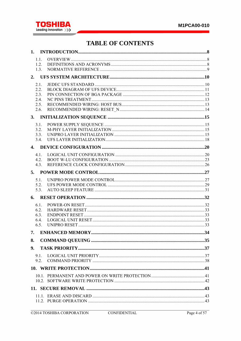
TABLE OF CONTENTS 1. INTRODUCTION .............................................................................................................8
1.1. OVERVIEW ............................................................................................................................. 8 1.2. DEFINITIONS AND ACRONYMS ........................................................................................ 8 1.3. NORMATIVE REFERENCE .................................................................................................. 9
2. UFS SYSTEM ARCHITECTURE ................................................................................10
2.1. JEDEC UFS STANDARD ..................................................................................................... 10 2.2. BLOCK DIAGRAM OF UFS DEVICE................................................................................. 11 2.3. PIN CONNECTION OF BGA PACKAGE ........................................................................... 12 2.4. NC PINS TREATMENT ........................................................................................................ 13 2.5. RECOMMENDED WIRING: HOST BUS ............................................................................ 13 2.6. RECOMMENDED WIRING: RESET_N .............................................................................. 14
3. INITIALIZATION SEQUENCE ..................................................................................15
3.1. POWER SUPPLY SEQUENCE ............................................................................................ 15 3.2. M-PHY LAYER INITIALIZATION ..................................................................................... 15 3.3. UNIPRO LAYER INITIALIZATION ................................................................................... 15 3.4. UFS LAYER INITIALIZATION ........................................................................................... 18
4. DEVICE CONFIGURATION .......................................................................................20
4.1. LOGICAL UNIT CONFIGURATION .................................................................................. 20 4.2. BOOT W-LU CONFIGURATION ........................................................................................ 23 4.3. REFERENCE CLOCK CONFIGURATION ......................................................................... 26
5. POWER MODE CONTROL .........................................................................................27
5.1. UNIPRO POWER MODE CONTROL .................................................................................. 27 5.2. UFS POWER MODE CONTROL ......................................................................................... 29 5.3. AUTO SLEEP FEATURE ..................................................................................................... 31
6. RESET OPERATION ....................................................................................................32
6.1. POWER-ON RESET .............................................................................................................. 32 6.2. HARDWARE RESET ............................................................................................................ 33 6.3. ENDPOINT RESET ............................................................................................................... 33 6.4. LOGICAL UNIT RESET ....................................................................................................... 33 6.5. UNIPRO RESET .................................................................................................................... 33
7. ENHANCED MEMORY ................................................................................................34
8. COMMAND QUEUING ................................................................................................35
9. TASK PRIORITY ...........................................................................................................37
9.1. LOGICAL UNIT PRIORITY ................................................................................................. 37 9.2. COMMAND PRIORITY ....................................................................................................... 38
10. WRITE PROTECTION .................................................................................................41
10.1. PERMANENT AND POWER ON WRITE PROTECTION ................................................. 41 10.2. SOFTWARE WRITE PROTECTION ................................................................................... 42
11. SECURE REMOVAL ....................................................................................................43
11.1. ERASE AND DISCARD ....................................................................................................... 43 11.2. PURGE OPERATION ........................................................................................................... 43

M1PCA00-010
©2014 TOSHIBA CORPORATION CONFIDENTIAL Page 5 of 57
11.3. WIPE DEVICE ....................................................................................................................... 45
12. RPMB ...............................................................................................................................46
12.1. AUTHENTICATION KEY PROGRAMMING .................................................................... 47 12.2. READ COUNTER VALUE ................................................................................................... 49 12.3. READ/WRITE RPMB DATA ............................................................................................... 50 12.4. RPMB MULTI FRAME FUNCTION (TOSHIBA SPECIFIC)............................................. 52
13. CONTEXT AND SYSTEM DATA TAG MANAGEMENT ......................................55
14. DATA SCRAMBLING ...................................................................................................55
DOCUMENT REVISION HISTORY...................................................................................56
RESTRICTIONS ON PRODUCT USE ................................................................................57

M1PCA00-010
©2014 TOSHIBA CORPORATION CONFIDENTIAL Page 6 of 57
LIST OF TABLES
Table 1 : Table of Acronyms ..............................................................................................8 Table 2 : Capacitance Values ............................................................................................12 Table 3 : Pin name description ..........................................................................................12 Table 4 : Link startup sequence ........................................................................................16 Table 5 : Related parameters about power-on sequence ...................................................18 Table 6 : Configuration descriptor format ........................................................................20 Table 7 : Configuration descriptor header and device descriptor configurable parameters
...................................................................................................................................20 Table 8 : Unit Descriptor configurable parameters ...........................................................21 Table 9 : Parameters related device capacity in Geometry Descriptor .............................22 Table 10 : Related parameters about boot operation ........................................................24 Table 11 : Available state for changing PA_HSSeries .....................................................28 Table 12 : START_STOP_UNIT command format .........................................................29 Table 13 : Summary of resets and device behavior ..........................................................32 Table 14 : Summary of resets and device behavior (2) ....................................................32 Table 15 : Task Management request UPIU format .........................................................33 Table 16 : Related parameters for Enhanced memory ......................................................34 Table 17 : Queue depth of LU, Boot W-LU, and RPMB W-LU ......................................35 Table 18 : Task Attribute definition ..................................................................................38 Table 19 : Related parameters about write protection ......................................................41 Table 20 : Control Mode Page format ..............................................................................42 Table 21 : Related parameters about secure removal .......................................................43 Table 22 : Difference between Erase and Discard operation ............................................43 Table 23 : Related parameters about Purge operation ......................................................45 Table 24 : RPMB Message data frame .............................................................................46 Table 25 : CDB format of Security Protocol In/Out commands ......................................46 Table 26 : Query Request UPIU and Data Frame Format for Multi Frame Function ......52 Table 27 : Query Response UPIU and Data Frame Format for Multi Frame Function ....53

M1PCA00-010
©2014 TOSHIBA CORPORATION CONFIDENTIAL Page 7 of 57
LIST OF FIGURES
Figure 1 : UFS Top Level Architecture ............................................................................10 Figure 2 : UFS System model ...........................................................................................11 Figure 3 : Block diagram of UFS device ..........................................................................11 Figure 4 : Pin connection of BGA package (Top View) ..................................................12 Figure 5 : Recommended wiring for TOSHIBA UFS device to a host ............................14 Figure 6 : Link startup sequence .......................................................................................17 Figure 7 : Initialization sequence ......................................................................................19 Figure 8 : Flow chart of writing Configuration Descriptor ...............................................22 Figure 9 : Flow chart of checking Boot W-LU .................................................................24 Figure 10 : Flow chart of setting Boot W-LU ...................................................................25 Figure 11 : UniPro power mode change sequence ............................................................28 Figure 12 : Power mode change from Active to Idle ........................................................30 Figure 13 : Power mode change from Idle to Active ........................................................30 Figure 14 : Power mode change to/from Sleep .................................................................31 Figure 15 : Host side handling of task overflow ...............................................................36 Figure 16 : Task dispatching order ...................................................................................37 Figure 17 : Task dispatching order in a LU ......................................................................38 Figure 18 : Task dispatching order in a LU with Ordered attribute task ..........................39 Figure 19 : Example of reordering among tasks with Simple attribute ............................39 Figure 20 : Example of reordering among tasks with Ordered attribute ..........................40 Figure 21 : Flow chart of write protection ........................................................................41 Figure 22 : Flow chart of Purge operation ........................................................................44 Figure 23 : Flow chart of Authentication Key programming ...........................................47 Figure 24 : Flow chart of Authentication Key programming verification ........................48 Figure 25 : Flow chart of read counter value ....................................................................49 Figure 26 : Flow chart of Authenticated Read ..................................................................50 Figure 27 : Flow chart of Authenticated write ..................................................................51 Figure 28 : Operation image with Multi Frame Function comparing with Single Frame 54

M1PCA00-010
©2014 TOSHIBA CORPORATION CONFIDENTIAL Page 8 of 57
1. Introduction
1.1. Overview
TOSHIBA’s UFS memory devies are one of the embedded memory solutions which use nonvolatile NAND flash memory devices for data storage and communication. It consists of NAND flash memory devices and a controller in single Ball Grid Array (BGA) package with the UFS interfaces.
UFS architecture is optimized for mobile devices, thus it has several advantages such as high-performance, low power consumption, low cost, fewer pin count, and small form factor. UFS adopts a protocol stacking structure, which uses MIPI M-PHYSM and UniProSM standards for lower layer protocol and SCSI architecture for upper layer protocol. The applications of the UFS cover a wide range of mobile devices such as mobile phones, Slate/Tablet PC, digital video cameras, MP3 player and PNDs, as well as other devices which need embedded memory devices inside.
TOSHIBA’s latest UFS is based upon JEDEC UFS standard version 2.0.
1.2. Definitions and Acronyms
Table 1 : Table of Acronyms
Acronyms Definition
BGA Ball Grid Array
CDB Command Descriptor Block
DME Device Management Entity
HCI Host Controller Interface
LU Logical Unit
LUN Logical Unit Number
MIPI Mobile Industry Processor Interface
MLC Multi Level Cell
NA Not applicable
PND Portable Navigation Device or Personal Navigation Device
PWM Pulse Width Modulation
RFU Reserved for future use
RPMB Replay Protected Memory Block
SBC SCSI Block Commands
SPC SCSI Primary Commands
UFS Universal Flash Interface
UniPro Unified Protocol.
UPIU UFS Protocol Information Unit
UTP UFS Transport Protocol
W-LU Well known logical unit

M1PCA00-010
©2014 TOSHIBA CORPORATION CONFIDENTIAL Page 9 of 57
1.3. Normative reference
This document refers following normative documents. For dated references, subsequent amendments to, or revisions of, any of these publications do not apply. For undated references, the latest edition of the normative document referred to applies.
[UFS] JEDEC Specification for UFS Version 2.0
[M-PHY] MIPI Alliance Specification for M-PHYSM Version 3.0
[UniPro] MIPI Alliance Specification for Unified Protocol (UniProSM) Version 1.6
[SAM] SCSI Architecture Model 5 (SAM‐5), Rev. 05, 19 May 2010
[SPC] T10 Specification: SCSI Primary Commands 4 (SPC-4), Rev.27, 11 October 2010
[SBC] T10 Specification: SCSI Block Commands 3 (SBC‐3), Rev.24, 05 August 2010

M1PCA00-010
©2014 TOSHIBA CORPORATION CONFIDENTIAL Page 10 of 57
2. UFS System Architecture
2.1. JEDEC UFS standard
JEDEC UFS standard adopts a protocol stacking structure like OSI reference model. M-PHYSM is adopted for physical layer, UniProSM is adopted for data link layer and network layer, transport layer, and UFS defines application layer. Also, UFS adopts Simplified SCSI command set based on SBC and SPC. It can save resources to develop driver software.
Figure 1 shows UFS top level architecture, and Figure 2 shows UFS System model.
Figure 1 : UFS Top Level Architecture
UFS standard defines Logical Unit which has an independent address space. Each LU processes SCSI tasks and performs task management functions independently. The LUs, which have same memory type, have independent address space logically, but physically share same memory space.
Maximum number of LU is 8 in the standard, and TOSHIBA UFS device also supports maximum 8 LUs.

M1PCA00-010
©2014 TOSHIBA CORPORATION CONFIDENTIAL Page 11 of 57
Figure 2 : UFS System model
2.2. Block Diagram of UFS device
TOSHIBA UFS device consists of raw MLC NAND chip(s) and a controller, which are put in a standard Ball Grid Array (BGA) package. Figure 3 shows an example of the block diagram of the UFS device, and specifications of capacitance in Figure 3 are listed in Table 2.
Figure 3 : Block diagram of UFS device

M1PCA00-010
©2014 TOSHIBA CORPORATION CONFIDENTIAL Page 12 of 57
Table 2 : Capacitance Values
Parameter Symbol Min. Typ Max. Unit
VCCQ2 internal regulator capacitor CVDDiQ2 0.7 2.2 2.4 μF
2.3. Pin connection of BGA package
The BGA package has 153 balls, and ball layout and pin assignments are compliant with JEDEC UFS standard. Figure 4 shows pin connections of the package of TOSHIBA UFS device.
Figure 4 : Pin connection of BGA package (Top View)
Table 3 : Pin name description
Name Type Description
VCC Supply Supply voltage for NAND chips
VCCQ Supply Supply voltage for memory controller
VCCQ2 Supply Supply voltage for NAND I/O interface and M-PHY interface
VDDi - Shall be connect to VCC or left floating
VDDiQ - Shall be connect to VCCQ or left floating

M1PCA00-010
©2014 TOSHIBA CORPORATION CONFIDENTIAL Page 13 of 57
VDDiQ2 Input Input terminal to provide bypass capacitor for VCCQ2 internal regulator
VSS Supply Ground
RESET_N Input Input hardware reset signal
REF_CLK Input Input reference clock. When not active, this signal should be pull-down or driven low by the host SoC.
DIN0/1_t Input Downstream data lane
DIN0/1_c Input Downstream data lane
DOUT0/1_t Output Upstream data lane
DOUT0/1_c Output Upstream data lane
CPOUT1/2 - No connection. Shall be connected to ground or left floating.
C+/C- - No connection. Shall be connected to ground or left floating.
RFU - Reserved for Future Use. Shall be connected to ground or left floating.
VSFn - Shall be left floating
2.4. NC Pins Treatment
Some of the NC pins are used in TOSHIBA’s internal testing. These pins are set to Hi-Z after product shipment and basically there should be no problem even if these pins are connected to GND or other signal line. (In case of connecting to a signal line, increase of capacitance has to be considered.)
2.5. Recommended Wiring: HOST BUS
DINn_t/c and DOUTn_t/c are high speed differential signals defined by MIPI M-PHY. These signals operate at maximum 5.8Gbps, therefore users have to pay enough attention for board layout.
DINn_t/c and DOUTn_t/c path between a host and a device should be designed for differential 100Ω (near 50Ω x 2) impedance to have loose coupling, and kept the length as short as possible. Each high speed differential signal pair should be placed 300μm far from other signals. TOSHIBA also recommends characterizing transmission lines by electromagnetic simulator.
If some of DINn_t/c or DOUTn_t/c are not used, the DINn_t/c is recommended to be connected to GND and DOUTn_t/c is recommended to be left floating.

M1PCA00-010
©2014 TOSHIBA CORPORATION CONFIDENTIAL Page 14 of 57
Figure 5 : Recommended wiring for TOSHIBA UFS device to a host
*1 : VDDi, VDDiQ, C+, C-, CPOUT1, and CPOUT2 pins are not used on TOSHIBA UFS devices.
2.6. Recommended Wiring: RESET_N
Specifications of the hardware reset timings are defined in the datasheet of each product. Users need to arrange the hardware reset wiring so as to satisfy the specifications. The appropriate value of RRST depends on system design.

M1PCA00-010
©2014 TOSHIBA CORPORATION CONFIDENTIAL Page 15 of 57
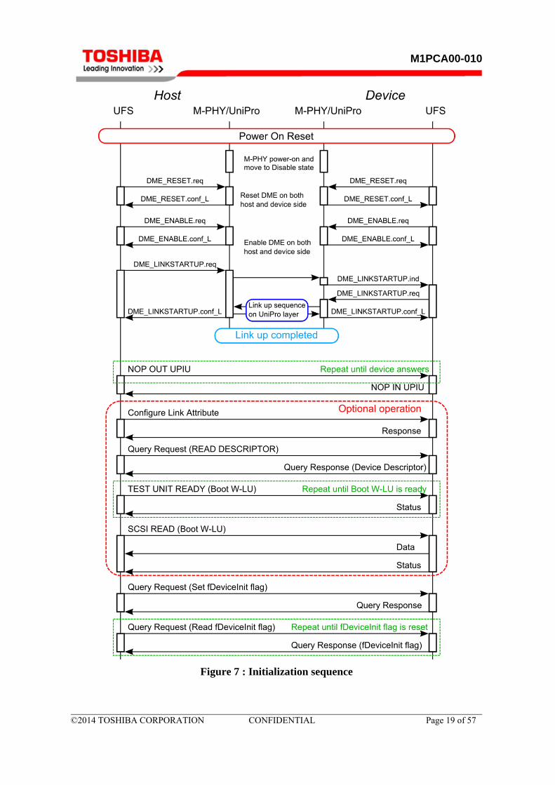
3. Initialization sequence UFS has layer stack architecture and power-on sequence takes place from lowest layer to highest layer.
3.1. Power supply sequence
TOSHIBA UFS device requires 3 power sources. Users need to satisfy the timing for applying power supplies defined in UFS standard and Technical Documentation of TOSHIBA UFS devices.
3.2. M-PHY layer initialization
After power-on or HW reset, M-PHY layer is initialized by itself on both host and device side automatically. After finishing M-PHY initialization, the layer is in Hibern8 state.
3.3. UniPro layer initialization
After power-on, HW reset, and DME_RESET, UniPro layer is in Disable state and is initialized in the following sequence.
1. Send DME_RESET.req primitive
2. Wait until DME_RESER.cnf_L is received
3. Send DME_ENABLE.req primitive
4. Wait until DME_ENABLE.cnf_L is received
5. Reset attributes to initial values
6. Send DME_LINKSTARTUP.req primitive
7. Wait until DME_LINKSTARTUP.req is received
TOSHIBA UFS devices support link startup initiation on both ends. Link startup is performed in PWM-G1. After link startup sequence is done successfully, the UniPro layer is in Linkup state, and its power mode is set to SlowAuto_Mode. Please refer to the following sequence for more information.

M1PCA00-010
©2014 TOSHIBA CORPORATION CONFIDENTIAL Page 16 of 57
Table 4 : Link startup sequence
Phase PA Transmitter PA Receiver
0 Continue to send TRG_UPR0 (all lanes) Wait for TRG_UPR0 reception. Lane discovery
0b Send two additional TRG_UPR1 Ignore all data
1 Continue to send TRG_UPR1 Wait for TRG_UPR1 reception on all lanes. Re-align Lane numbering
2 Send two additional TRG_UPR1. Then proceed with phase 3.
Ignore all data
3 Continue to send TRG_UPR2 on all lanes
Wait for TRG_UPR2 reception on PHY RX Data Lane 0. - TRG_UPR1 (M-PHY: ignored) - Others (M-PHY: ignored) - TRG_UPR2 (Phase 4)
4 Send two additional TRG_UPR2 on all lanes. Then proceed with Phase 5.
Ignore all data
5
Transfer Capabilities, Initiate Capability transfer of potential Media Converter.
Receive Capabilities and apply down grading
Report to the DME using PA_LM_LINKSTARTUP.cnf_L that the Link Startup Sequence succeeded. Exit the Link Startup Sequence and enter SlowAuto_Mode.

M1PCA00-010
©2014 TOSHIBA CORPORATION CONFIDENTIAL Page 17 of 57
Figure 6 : Link startup sequence

M1PCA00-010
©2014 TOSHIBA CORPORATION CONFIDENTIAL Page 18 of 57
3.4. UFS layer initialization
After UniPro and M-PHY initialization, the following sequence needs to be executed to initialize UFS layer.
1. Send NOP OUT UPIU to confirm that a UFS device is ready to receive UPIU. * When a device is ready, a single NOP IN UPIU is returned to a host as a response. If a response is not returned, please try to send NOP OUT UPIU from a host again.
2. If necessary, do the following optional operation.
(2-1) Configure the Link Attribute (i.e. Gear, HS Series, PWM Mode in TX and RX)
(2-2) Read Device Descriptor. (Only when bDescrAccessEn = 01h)
(2-3) Download the boot code from Boot W-LU. (In case that Boot LU is enable and boot code is already written.)
3. Set 01h to fDeviceInit flag, and poll this flag until the device clear it.
After the sequence is done successfully, the UFS layer moves to the state defined by bInitPowerMode in Device Descriptor. At the time of shipment of the device, all logical units except for RPMB well known logical units are disabled. So, users need to configure Unit Descriptors once and activate the setting of the descriptors by a power cycle. Please refer to Section 4.1 for more information.
Table 5 : Related parameters about power-on sequence
Offset Size Name Description
Device Descriptor
09h 1 bDescrAccessEn 00h: Device Descriptor access disabled 01h: Device Descriptor access enabled
0Ah 1 bInitPowerMode 00h: UFS-Sleep Mode 01h: Active Mode
Flags
01h 1 fDeviceInit 0b: Device initialization completed or not started yet.
1b: Device initialization in progress.
After logical unit configuration, a host can access to the configured logical units, but the condition of each logical unit is UNIT ATTENTION as initial condition. If a host issues a command in this condition, a device returns a response of CHECK CONDITION status with the sense key of UNIT ATTENTION. So, it is recommended that REQUEST SENSE command is issued once for each logical unit before accessing them. In this case, the device returns a response with the status of GOOD and clears UNIT ATTENTION condition.
M1PCA00-010
©2014 TOSHIBA CORPORATION CONFIDENTIAL Page 19 of 57
Figure 7 : Initialization sequence

M1PCA00-010
©2014 TOSHIBA CORPORATION CONFIDENTIAL Page 20 of 57
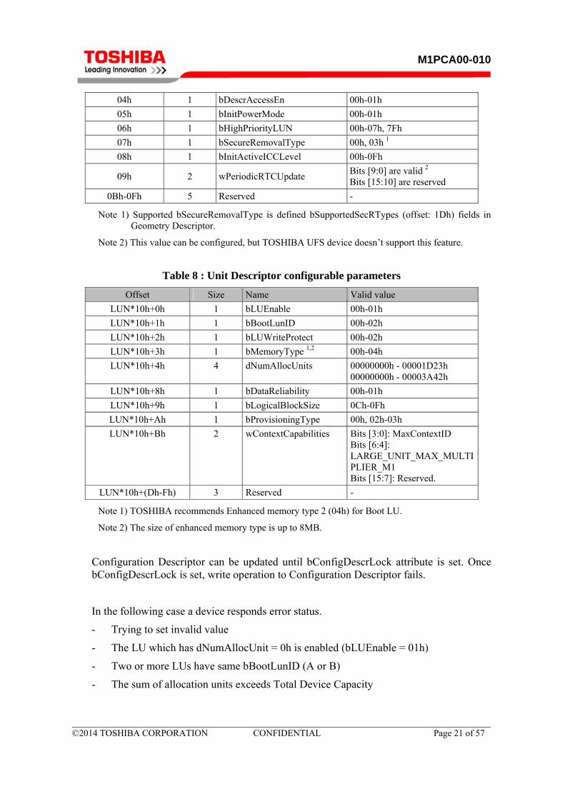
4. Device configuration UFS standard defines a block of parameters, Descriptor, which specifies the composition of a device. Most of descriptors are read only, but some of them can be configured by users. Basically, these configurable descriptors need to be configured during system design. This chapter provides information on how to configure the descriptors.
4.1. Logical unit configuration
TOSHIBA UFS device supports maximum 8 logical units so that users can configure the memory area of the device according to their usage. Each logical unit has different memory space and it can be used like a partition.
At the time of shipment of the device, all logical units except for RPMB well known logical units are disabled. Therefore users must set following configurable parameters in Device Descriptor and Unit Descriptor before accessing logical units. Configured parameters are valid after a power cycle.
Configurable parameters
Table 6 shows Configuration Descriptor Format. Configuration parameters consist of Configuration Descriptor header, parameters of Device Descriptor, and parameters of Unit Descriptor.
Table 6 : Configuration descriptor format
Offset Description
00h-0Fh 1 Configuration Descriptor header and Device Descriptor configurable parameters
10h-1Fh 1 Unit Descriptor 0 configurable parameters
: :
: :
80h-8Fh 1 Unit Descriptor 7 configurable parameters
Note 1) Offset values depend on bUD0BaseOffset and bUDConfigPLength parameters in Device Descriptor. UFS standard defines both values are 10h.
Table 7 : Configuration descriptor header and device descriptor configurable parameters
Offset Size Name Valid value
00h 1 bLength 90h (Fixed)
01h 1 bDescriptorType 01h (Fixed)
02h 1 Reserved
03h 1 bBootEnable 00h-01h
M1PCA00-010
©2014 TOSHIBA CORPORATION CONFIDENTIAL Page 21 of 57
04h 1 bDescrAccessEn 00h-01h
05h 1 bInitPowerMode 00h-01h
06h 1 bHighPriorityLUN 00h-07h, 7Fh
07h 1 bSecureRemovalType 00h, 03h 1
08h 1 bInitActiveICCLevel 00h-0Fh
09h 2 wPeriodicRTCUpdate Bits [9:0] are valid 2 Bits [15:10] are reserved
0Bh-0Fh 5 Reserved -
Note 1) Supported bSecureRemovalType is defined bSupportedSecRTypes (offset: 1Dh) fields in Geometry Descriptor.
Note 2) This value can be configured, but TOSHIBA UFS device doesn’t support this feature.
Table 8 : Unit Descriptor configurable parameters
Offset Size Name Valid value
LUN*10h+0h 1 bLUEnable 00h-01h
LUN*10h+1h 1 bBootLunID 00h-02h
LUN*10h+2h 1 bLUWriteProtect 00h-02h
LUN*10h+3h 1 bMemoryType 1,2 00h-04h
LUN*10h+4h 4 dNumAllocUnits 00000000h - 00001D23h 00000000h - 00003A42h
LUN*10h+8h 1 bDataReliability 00h-01h
LUN*10h+9h 1 bLogicalBlockSize 0Ch-0Fh
LUN*10h+Ah 1 bProvisioningType 00h, 02h-03h
LUN*10h+Bh 2 wContextCapabilities Bits [3:0]: MaxContextID Bits [6:4]: LARGE_UNIT_MAX_MULTIPLIER_M1 Bits [15:7]: Reserved.
LUN*10h+(Dh-Fh) 3 Reserved -
Note 1) TOSHIBA recommends Enhanced memory type 2 (04h) for Boot LU.
Note 2) The size of enhanced memory type is up to 8MB.
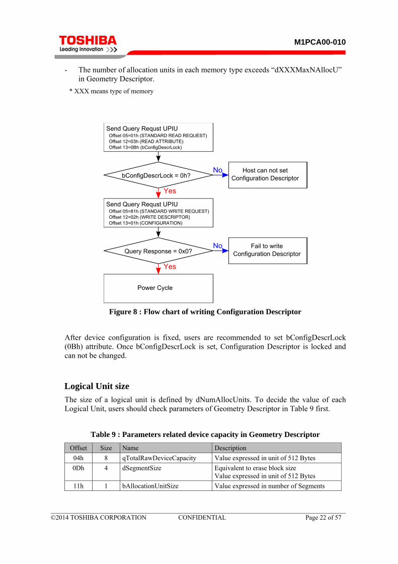
Configuration Descriptor can be updated until bConfigDescrLock attribute is set. Once bConfigDescrLock is set, write operation to Configuration Descriptor fails.
In the following case a device responds error status.
- Trying to set invalid value
- The LU which has dNumAllocUnit = 0h is enabled (bLUEnable = 01h)
- Two or more LUs have same bBootLunID (A or B)
- The sum of allocation units exceeds Total Device Capacity
M1PCA00-010
©2014 TOSHIBA CORPORATION CONFIDENTIAL Page 22 of 57
- The number of allocation units in each memory type exceeds “dXXXMaxNAllocU” in Geometry Descriptor.
* XXX means type of memory
Figure 8 : Flow chart of writing Configuration Descriptor
After device configuration is fixed, users are recommended to set bConfigDescrLock (0Bh) attribute. Once bConfigDescrLock is set, Configuration Descriptor is locked and can not be changed.
Logical Unit size
The size of a logical unit is defined by dNumAllocUnits. To decide the value of each Logical Unit, users should check parameters of Geometry Descriptor in Table 9 first.
Table 9 : Parameters related device capacity in Geometry Descriptor
Offset Size Name Description
04h 8 qTotalRawDeviceCapacity Value expressed in unit of 512 Bytes
0Dh 4 dSegmentSize Equivalent to erase block size Value expressed in unit of 512 Bytes
11h 1 bAllocationUnitSize Value expressed in number of Segments

M1PCA00-010
©2014 TOSHIBA CORPORATION CONFIDENTIAL Page 23 of 57
Total Device Capacity = qTotalRawDeviceCapacity * 512[Byte]
Physical Erase Block Size = dSegmentSize * 512 [Byte]
Allocation Unit Size = bAllocationUnitSize * (Physical Erase Block Size)
Capacity of a Logical Unit = dNumAllocUnits* (Allocation Unit Size) / CapAdjFac * CapAdjFac = 1 for Normal memory type
In addition, also check the following parameters if memory type is other than Normal memory type. CapAdjFac of each memory type is calculated from the parameters.
- dSystemCodeMaxNAllocU, wSystemCodeCapAdjFac
- dNonPersistMaxNAllocU, wNonPersistCapAdjFac * Not supported in TOSHIBA UFS device
- dEnhanced’X’MaxNAllocU, wEnhanced’X’CapAdjFac: ’X’ is 1~4
Provisioning type
UFS standard defines 2 provisioning types. One is full provisioning and the other is thin provisioning. TOSHIBA UFS device supports both provisioning types. When bProvisioningType parameter is set to 00h (full provisioning), all logical block addresses are mapped physically, and UNMAP command is not supported. When bProvisioningType parameter is set to 02h or 03h (thin provisioning), logical block addresses are mapped or deallocated, and UNMAP command is supported. In case of thin provisioning, the device behavior for UNMAP command is different depending on the value of bProvisioningType. Please refer to Section 11 for more information. TOSHIBA recommends the use of thin provisioning functionality in the performance point of view.
4.2. Boot W-LU configuration
2 logical units (Boot LU A, Boot LU B) can be used to store the boot code, but only one of them is active during the boot process. Any logical unit can be configured as “Boot LU A” or “Boot LU B”, but 2 or more than logical units can not be assigned to the same Boot LU. The logical unit that is active during boot is mapped onto the Boot well known logical unit (W-LUN = 30h) for read access. Users can confirm whether Boot W-LU is enabled or not by using TEST UNIT READY command.

M1PCA00-010
©2014 TOSHIBA CORPORATION CONFIDENTIAL Page 24 of 57
Figure 9 : Flow chart of checking Boot W-LU
Enable Boot well known LU
At the time of shipment of the device, Boot W-LU is disabled because all logical units are configured. So, users need to set bBootEnable in Device Descriptor, bBootLunID and bMemoryType in Unit Descriptor, and bBootLunEn attribute to enable boot operation.
TOSHIBA recommends to set Boot well known logical unit as Enhanced memory type 2 (bMemoryType = 04h). The maximum size of enhance memory type 2 is 8MB, so please set the total logical size of Boot well know LU so that it does not exceed 8MB.
Table 10 : Related parameters about boot operation
Offset Size Name Description
Device Descriptor
03h 1 bDeviceClass 00h: Mass Storage
04h 1 bDeviceSubClass 00h: Embedded Bootable
08h 1 bBootEnable 01h: Bootable feature enabled
Unit Descriptor
03h 1 bLUEnable 01h: Logical Unit enabled
04h 1 bBootLunID 01h: Boot LU A 02h: Boot LU B
08h 1 bMemoryType
00h: Normal Memory 01h: System code memory type 02h: Non-Persistent memory type 03h: Enhanced memory type 1 04h: Enhanced memory type 2
(recommended for Boot LU)
IDN Size Name Description
Attribute
00h 1 bBootLunEn 01h: Enabled boot from Boot LU A 02h: Enabled boot from Boot LU B

M1PCA00-010
©2014 TOSHIBA CORPORATION CONFIDENTIAL Page 25 of 57
Figure 10 : Flow chart of setting Boot W-LU

M1PCA00-010
©2014 TOSHIBA CORPORATION CONFIDENTIAL Page 26 of 57
Programming boot code to the device
Boot W-LU (W-LUN = 30h) is a read-only logical unit, therefore it’s prohibited to write data directly. So, a boot code needs to be programmed to a logical unit of which bBootLunID parameter in Unit Descriptor is 01h or 02h. Programmed data to a logical unit which has bBootLunID = 01h or 02h is read through Boot W-LU.
4.3. Reference clock configuration
TOSHIBA UFS device supports 19.2, 26, 38.4, 52MHz reference clock. The default value is 26MHz. The frequency of reference clock is defined by bRefClkFreq attribute. If a host uses reference clock different from 26MHz, bRefClkFreq should be configured during UFS layer initialization. Please note that bRefClkFreq is write-once attribute.
M1PCA00-010
©2014 TOSHIBA CORPORATION CONFIDENTIAL Page 27 of 57
5. Power mode control UFS standard defines several power modes, and UniPro/M-PHY also defines their own power modes. Both UFS and UniPro/M-PHY power modes are not linked each other, so a host needs to control the power modes independently. The change of power mode in UFS layer is done by issuing SCSI command, while the change of power mode in UniPro layer is done via DME. M-PHY power states are controlled by UniPro depending on UniPro power mode setting, so a host doesn’t need to control M-PHY power state directly. The control of each layer’s power mode is important to minimize device power consumption. TOSHIBA UFS device supports all power modes defined in UFS and UniPro standard.
5.1. UniPro power mode control
UniPro standard defines 6 power modes and a host controls the power modes by attributes and DME requests. UniPro also has “Power States”, but these are not configured by a host because the power states automatically change according to the power mode setting.
Fast_Mode, Slow_Mode, FastAuto_Mode, and SlowAuto_Mode
The power mode change between Fast_Mode, Slow_Mode, FastAuto_Mode, and SlowAuto_Mode is controlled by DME_POWERMODE or DME_SET primitive, but DME_POWERMODE cannot be used because UFS HCI standard.
Setting PA_PWMMode attribute by DME_SET triggers UniPro power mode change between Fast_Mode, Slow_Mode, FastAuto_Mode, and SlowAuto_Mode. So, a host needs to set attributes relative to power mode before setting PA_PWMMode.

M1PCA00-010
©2014 TOSHIBA CORPORATION CONFIDENTIAL Page 28 of 57
Figure 11 : UniPro power mode change sequence
Please note that TOSHIBA UFS device doesn’t support to change PA_HSSeries during HS-mode operation.
Table 11 : Available state for changing PA_HSSeries
to
PWM HS
G1 G2 G3 G4 G1A G2A G1B G2B
from
PWM
G1 Yes Yes Yes Yes Yes Yes Yes Yes
G2 Yes Yes Yes Yes Yes Yes Yes Yes
G3 Yes Yes Yes Yes Yes Yes Yes Yes
G4 Yes Yes Yes Yes Yes Yes Yes Yes
HS
G1A Yes Yes Yes Yes Yes Yes No No
G2A Yes Yes Yes Yes Yes Yes No No
G1B Yes Yes Yes Yes No No Yes Yes
G2B Yes Yes Yes Yes No No Yes Yes
Hibernate mode
Hibernate enter and hibernate exit procedures are different form normal Power Mode change operation. The power mode of UniPro changes to Hibernate mode by performing DME_HIBERNATE_ENTER on a host via HCI. During the transition to Hibernate mode, UniPro changes the Power State of M-PHY to Hibern8 state. UniPro exits from Hibernate mode by DME_HIBERNATE_EXIT on a host via HCI.

M1PCA00-010
©2014 TOSHIBA CORPORATION CONFIDENTIAL Page 29 of 57
When entering to Hibernate mode, the current Power Mode configuration including M-PHY settings and lane count information are stored. They are automatically restored when exiting Hibernate mode.
5.2. UFS power mode control
UFS standard defines 4 basic power modes, that is Active, Idle, Sleep, and Power down. These power modes are controlled by POWER CONDITION field in START_ STOP_UNIT command and some attributes. To change the device power mode, send the command to UFS Device W-LUN (LUN: D0h). Current power mode can be checked by bCurrentPowerMode Attribute (IDN: 02h).
Also logical units can be stopped individually using this command.
Table 12 : START_STOP_UNIT command format
Bit Byte
7 6 5 4 3 2 1 0
0 OPERATION CODE (1Bh)
1 Reserved IMMED
2 Reserved
3 Reserved Reserved
4 POWER CONDITION Resv. NO_
FLUSHLOEJ =0b
START
5 CONTROL (00h)
Care also NO_FLUSH field when the device power mode is changed. When the device power mode is changed, all dynamic data including cached data might be lost if NO_FLUSH field is set (=1b).
Active power mode
All operations accessing storage work in this mode. The device moves to this mode via Pre-Active when the device receives START_STOP_UNIT command that power condition field is 01h. When a UFS host does not access for a certain period of time, the device moves to Idle power mode automatically.
Idle power mode
Idle power mode is transited from Active power mode only, and automatically move to Active power mode when the device needs to execute any tasks. To minimize power consumption in this power mode, UniPro power state is recommended to be Hibernate.

M1PCA00-010
©2014 TOSHIBA CORPORATION CONFIDENTIAL Page 30 of 57
Figure 12 : Power mode change from Active to Idle
Figure 13 : Power mode change from Idle to Active
UFS-Sleep power mode
The power mode moves from Active power mode via Pre-Sleep when the device receives START_STOP_UNIT command that power condition field is 02h. In this mode, VCC power supply can be removed.

M1PCA00-010
©2014 TOSHIBA CORPORATION CONFIDENTIAL Page 31 of 57
Figure 14 : Power mode change to/from Sleep
UFS-PowerDown power mode
The power mode moves from Active or Sleep power mode via Pre-PowerDown when the device receives START_STOP_UNIT command that power condition field is 03h. All power supplies can be removed. In generally, the device should be entered in this mode before power-off.
5.3. Auto Sleep feature
Auto Sleep is a feature to makes the TOSHIBA UFS device automatically enter into the low power consumption mode when there is no command for a certain period. The period until the TOSHIBA UFS device shifts into the Auto Sleep mode since the last command occurred is defined as auto sleep shift time (TA: 10ms).

M1PCA00-010
©2014 TOSHIBA CORPORATION CONFIDENTIAL Page 32 of 57
6. Reset operation TOSHIBA UFS device supports 5 types of reset as follows.
Table 13 : Summary of resets and device behavior
Reset type Valid
Power Mode
Power mode after reset
Boot process bInitPowerMode = 00h
bInitPowerMode = 01h
Power-on reset Any Pre-Sleep Pre-Active Enabled
Hardware reset Any Pre-Sleep Pre-Active Enabled
Endpoint reset Any Pre-Sleep Pre-Active Enabled
Logical Unit reset Active/Idle Same as prev. Same as prev. Disabled
UniPro reset Any Pre-Sleep Pre-Active Enabled
Table 14 : Summary of resets and device behavior (2)
Reset Type UniPro Stack and Attributes
Volatile and Set Only Attributes and Flags
Power on reset Attributes and Flags
Logical Unit Queue
Power-on reset Reset Reset Reset Reset (all logical units)
Hardware reset Reset Reset Reset Reset (all logical units)
Endpoint reset Reset Reset Not affected Reset (all logical units)
Logical Unit reset Not affected Not affected Not affected Reset (addressed logical unit)
UniPro reset Reset Reset No affected Reset (all logical units)
6.1. Power-on reset
TOSHIBA UFS device runs Power-on reset operation after switching VCC, VCCQ, or VCCQ2 power supplies off and back on. All Descriptors, Attributes, and Flags are reset and the device processes initialization sequence. VCC power supply can be off when the device is UFS Sleep or PowerDown power mode, and VCCQ and VCCQ2 power supplies can be off when the device is UFS PowerDown power mode. If power supplies are off other than above condition, internal NAND chips might be damaged and automatically perform unexpected shutdown recovery sequence in next power-on sequence.

M1PCA00-010
©2014 TOSHIBA CORPORATION CONFIDENTIAL Page 33 of 57
6.2. Hardware Reset
When a RESET_N pin is set to low for a certain period, the device runs Hardware reset operation. All volatile information including queued tasks is lost after this reset. Hardware reset timing is defined in Technical Documentation of TOSHIBA UFS devices.
6.3. Endpoint reset
When the device receives DME_ENDPOINTRESET from a host, it runs Endpoint reset operation. All volatile information including queued tasks is lost after this reset. This reset is a kind of software reset for the device.
6.4. Logical Unit reset
Logical Unit reset is executed by Task Management Request UPIU. To apply this reset, set Task Management Function field in Task Management Request UPIU to 08h (Logical Unit Reset). Only a specified logical unit can be reset and all queued tasks in the logical unit are cancelled. This reset does not affect the device parameters such as attributes and flags.
Table 15 : Task Management request UPIU format
Task Management Request UPIU
0 xx00 0100b
1 Flags
2 LUN
3 Task Tag
4
Reserved
5
Task Manag. Func.
6
Reserved
7
Reserved
8
Total EHS Length
9
Reserved
10-11
Data Segment Length (0000h)
12-15
Input parameter 1
….
6.5. UniPro reset
A host can reset its own UniPro layer via the DME_LINKLOST message. Once the device receives DME_LINKLOST message from the host, it starts process of re-initializing its own UniPro layer. All UFS level activity has been aborted and all task queue lists are cleared.

M1PCA00-010
©2014 TOSHIBA CORPORATION CONFIDENTIAL Page 34 of 57
7. Enhanced memory TOSHIBA UFS device supports Enhanced memory type 1 and 2. Enhanced memory type 2 is optimized for sequential access, therefore TOSHIBA recommends using Enhanced memory type 2 for Boot logical unit. Each logical unit can be set to enhanced option by Configuration Descriptor.
Table 16 : Related parameters for Enhanced memory
Offset Size Name Description
Unit Descriptor
08h 1 bMemoryType 00h: Normal Memory 01h: System code memory type 02h: Non-Persistent memory type 03h: Enhanced memory type 1 04h: Enhanced memory type 2
(recommended for Boot LU)
Geometry Descriptor
1Eh 2 wSupportedMemoryTypes Bit 0: Normal Memory Bit 1: System code memory type Bit 2: Non-Persistent memory type Bit 3: Enhanced memory type 1 Bit 4: Enhanced memory type 2
2Ch 4 dEnhanced1MaxNAllocU Max Number of Allocation Units for the Enhanced memory type 1
30h 2 wEnhanced1CapAdjFac Capacity Adjustment Factor for the Enhanced memory type 1
32h 4 dEnhanced2MaxNAllocU Max Number of Allocation Units for the Enhanced memory type 2
36h 2 wEnhanced2CapAdjFac Capacity Adjustment Factor for the Enhanced memory type 2

M1PCA00-010
©2014 TOSHIBA CORPORATION CONFIDENTIAL Page 35 of 57
8. Command Queuing TOSHIBA UFS device supports command queuing feature. The received tasks are queued into the task queue that each logical unit has independently. The order of the tasks is decided by task priority and command priority. Please refer to Chapter 9 for more information about task priority.
The queue depth of each logical unit is determined by the number of enabled logical units excluding the logical units configured as Boot LU. The values can be read from bLUQueueDepth in Unit Descriptor. RPMB W-LU is also dependent on the number of enabled logical units, but Boot W-LU is not. Please refer to Table 17 for more information.
Table 17 : Queue depth of LU, Boot W-LU, and RPMB W-LU
Queue depth
(A) 2 or more enabled logical units 1 (B) 1 enabled logical unit 1
LU 8 32
Boot W-LU 8 8
RPMB W-LU 2 2 8 2
Note 1) The number of enabled logical units excludes the logical units configured as Boot LU.
Note 2) The values are actual TOSHIBA UFS device implementation, but bLUQueueDepth in RPMB UNIT DESCRIPTOR is 00h because UFS standard defines it.
If a host sends more commands than queue depth in the logical unit, the device returns a RESPONSE UPIU with Target Failure (01h) in Response field and TASK SET FULL (28h) in Status field. If more commands are sent form a host, a device ignore the commands and returns no error. So, a host needs to handle the number of tasks depending on queue depth.

M1PCA00-010
©2014 TOSHIBA CORPORATION CONFIDENTIAL Page 36 of 57
Figure 15 : Host side handling of task overflow

M1PCA00-010
©2014 TOSHIBA CORPORATION CONFIDENTIAL Page 37 of 57
9. Task priority TOSHIBA UFS device has two types of task priority. One is a logical unit priority and the other is a command priority defined in SCSI Architecture Model-5 specification.
9.1. Logical Unit priority
Each logical unit has a High or Normal priority which is decided by bHighPriorityLUN in Device Descriptor. When bHighPriorityLUN is set to any one of 00h-07h, the corresponding logical unit is handled as a high priority logical unit. When bHighPriorityLUN is default value (7Fh), all logical units are handled as normal priority.
The queued tasks in high priority logical unit are preferentially handled than the tasks in other logical units and the tasks in other logical units wait until all tasks in high priority logical unit are completed.
In case of Figure 16, dispatching order is;
1. Task x_1 (x: 0-7)
2. Task 0_2, Task 0_3
3. Rest of tasks
Figure 16 : Task dispatching order
Tasks in dispatching state (0_1 to 7_1) are continued processing even if tasks for high priority LU come, but tasks in waiting state does not move to dispatching state until all tasks for high priority logical unit finish.
The processing order of tasks in same priority logical units is decided by device itself. Task 1_3 must be executed after Task 1_2, but Task 1_2 might be executed before Task 7_2 and also might be executed after Task 7_3.
M1PCA00-010
©2014 TOSHIBA CORPORATION CONFIDENTIAL Page 38 of 57
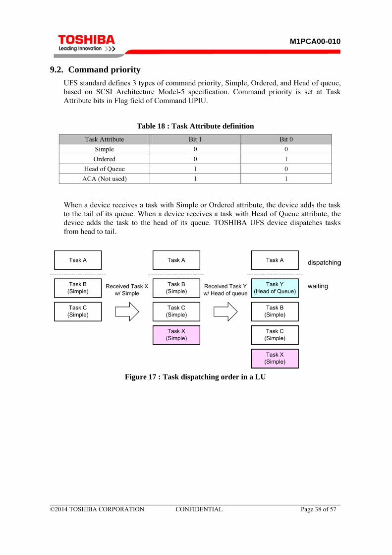
9.2. Command priority
UFS standard defines 3 types of command priority, Simple, Ordered, and Head of queue, based on SCSI Architecture Model-5 specification. Command priority is set at Task Attribute bits in Flag field of Command UPIU.
Table 18 : Task Attribute definition
Task Attribute Bit 1 Bit 0
Simple 0 0
Ordered 0 1
Head of Queue 1 0
ACA (Not used) 1 1
When a device receives a task with Simple or Ordered attribute, the device adds the task to the tail of its queue. When a device receives a task with Head of Queue attribute, the device adds the task to the head of its queue. TOSHIBA UFS device dispatches tasks from head to tail.
Figure 17 : Task dispatching order in a LU
M1PCA00-010
©2014 TOSHIBA CORPORATION CONFIDENTIAL Page 39 of 57
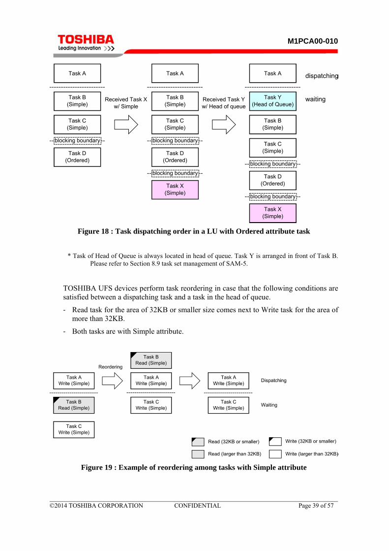
Figure 18 : Task dispatching order in a LU with Ordered attribute task
* Task of Head of Queue is always located in head of queue. Task Y is arranged in front of Task B. Please refer to Section 8.9 task set management of SAM-5.
TOSHIBA UFS devices perform task reordering in case that the following conditions are satisfied between a dispatching task and a task in the head of queue.
‐ Read task for the area of 32KB or smaller size comes next to Write task for the area of more than 32KB.
‐ Both tasks are with Simple attribute.
Figure 19 : Example of reordering among tasks with Simple attribute

M1PCA00-010
©2014 TOSHIBA CORPORATION CONFIDENTIAL Page 40 of 57
On the contrary, reordering does not take place in the condition of the combination of “read-read”, “write-write”, and “write after read” regardless of the task size. As for the combination of “read after write”, reordering does not take place if any one of the tasks is with Ordered attribute.
Figure 20 : Example of reordering among tasks with Ordered attribute

M1PCA00-010
©2014 TOSHIBA CORPORATION CONFIDENTIAL Page 41 of 57
10. Write Protection TOSHIBA UFS device supports 3 types of write protection. They are Permanent write protection, Power on write protection, and Software write protection. A logical unit is write- protected when at least one of them is set.
10.1. Permanent and Power on write protection
fPermanentWPEn is a write once flag, so it is never cleared once it is set. On the contrary, fPowerOnWPEn is set only one time during operation and is cleared by a power cycle or hardware reset only. Query Request to overwrite fPowerOnWPEn is failed and Response field is set to F8h (Parameter already written).
Figure 21 : Flow chart of write protection
Table 19 : Related parameters about write protection
Offset Size Name Description
Unit Descriptor
05h 1 bLUWriteProtect
00h: LU not write protected 01h: LU write protected when
fPowerOnWPEn = 1 02h: LU permanently write protected when
fPermanentWPEn = 1
Flags
02h - fPermanentWPEn 0b: Permanent write protection disabled 1b: Permanent write protection enabled
03h - fPowerOnWPEn 0b: Power on write protection disabled. 1b: Power on write protection enabled.

M1PCA00-010
©2014 TOSHIBA CORPORATION CONFIDENTIAL Page 42 of 57
10.2. Software write protection
This feature is provided by Control Mode Page. The device can be protected through MODE SELECT command to the page. SWP bit set to one specifies that the logical unit is protected from write operations. Otherwise the logical unit is not protected if permanent or power-on write protection is not set. This setting is automatically cleared after any reset operations except for UniPro reset.
Table 20 : Control Mode Page format
Bit Byte
7 6 5 4 3 2 1 0
0 PS (0b) 0b PAGE CODE (0Ah)
1 PAGE LENGTH (0Ah)
2 TST 0b 0b 0b 0b 0b
3 QUEUE ALGORITHM MODIFIER
(0001b) 0b 00b 0b
4 0b 0b 00b SWP 000b
….

M1PCA00-010
©2014 TOSHIBA CORPORATION CONFIDENTIAL Page 43 of 57
11. Secure removal UFS device supports some security features like e-MMCTM. bSecureRemovalType in Device Descriptor defines the method to remove secure data. Supported secure removal types are defined at bSupportedSecRTypes parameter in Geometry Descriptor. Secure removal features can be used only when bProvisioningType is 02h or 03h.
Table 21 : Related parameters about secure removal
Offset Size Name Description
Device Descriptor
0Ch 1 bSecureRemovalType 00h: information removed by an erase of the physical memory
03h: information removed using a vendor define mechanism.
Geometry Descriptor
1Dh 1 bSupportedSecRTypes bit 0-3: Supported bSecureRemovalType
11.1. Erase and Discard
Erase and Discard operations run when the device receives UNMAP command. The device executes Erase operation when bProvisioningType is 03h, and executes Discard operation when bProvisioningType is 02h. UNMAP command shall be failed when bProvisioningType is 00h, therefore these operations never run.
Table 22 : Difference between Erase and Discard operation
Operation Condition Description
Erase bProvisioningType = 03h
Runs when the device receives UNMAP command. The
device returns all ‘0’ when erased address is read.
Discard bProvisioningType = 02h
Runs when the device receives UNMAP command. The device may return any value, including the original data when discarded address is read.
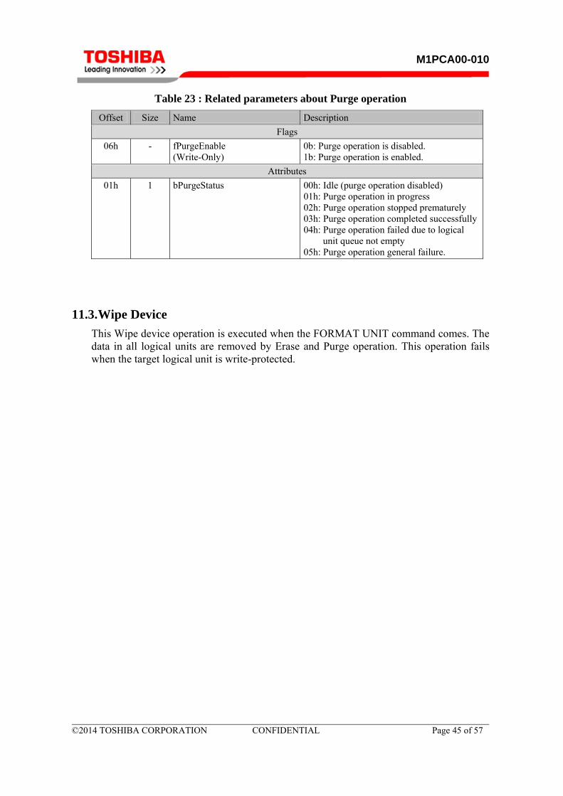
11.2. Purge operation
The Purge operation operates for the unmapped address space. When the operation is executed, all the data are removed from the unmapped address space. Purge operation runs when fPurgeEnable Flag is set and command queue in all LUs are empty. The status of Purge operation can be checked by bPurgeStatus Attribute. Basically this operation takes long time and any command shall be failed during this operation. A host can interrupt this operation by clearing fPurgeEnable Flag.

M1PCA00-010
©2014 TOSHIBA CORPORATION CONFIDENTIAL Page 44 of 57
Figure 22 : Flow chart of Purge operation
M1PCA00-010
©2014 TOSHIBA CORPORATION CONFIDENTIAL Page 45 of 57
Table 23 : Related parameters about Purge operation
Offset Size Name Description
Flags
06h - fPurgeEnable (Write-Only)
0b: Purge operation is disabled. 1b: Purge operation is enabled.
Attributes
01h 1 bPurgeStatus 00h: Idle (purge operation disabled) 01h: Purge operation in progress 02h: Purge operation stopped prematurely 03h: Purge operation completed successfully04h: Purge operation failed due to logical
unit queue not empty 05h: Purge operation general failure.
11.3. Wipe Device
This Wipe device operation is executed when the FORMAT UNIT command comes. The data in all logical units are removed by Erase and Purge operation. This operation fails when the target logical unit is write-protected.

M1PCA00-010
©2014 TOSHIBA CORPORATION CONFIDENTIAL Page 46 of 57
12. RPMB UFS device supports RPMB W-LU. RPMB W-LU is always enabled, and accessed via SECURITY PROTOCOL IN/OUT command. The parameters about RPMB can be checked in RPMB Unit Descriptor. The RPMB W-LU size of the device can be calculated from following parameters;
Logical Block Size: 256Bytes (bLogicalBlockSize)
Total RPMB Capacity: bLogicalBlockSize * qLogicalBlockCount (in RPMB Unit Descriptor)
Table 24 : RPMB Message data frame
Byte position Content
0-195 Stuff Bytes (196B)
196-227 Key/MAC (32B)
228-483 Data (256B)
484-499 Nonce (16B)
500-503 Write Counter (4Bytes)
504-505 Address (2Bytes)
506-507 Block Count (2Bytes)
508-509 Result (2Bytes)
510-511 Request/Response (2Bytes)
Table 25 : CDB format of Security Protocol In/Out commands
Bit Byte
7 6 5 4 3 2 1 0
0 OPERATION CODE (A2h/B5h)
1 SECURITY PROTOCOL (ECh)
2 SECURITY PROTOCOL SPECIFIC (0001h)
3
4 0b Reserved
5 Reserved
6 (MSB)ALLOCATION / TRANSFER LENGTH
9 (LSB)
10 Reserved
11 CONTROL = 00h

M1PCA00-010
©2014 TOSHIBA CORPORATION CONFIDENTIAL Page 47 of 57
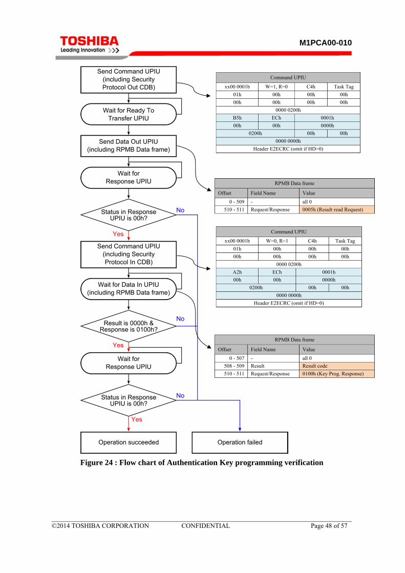
12.1. Authentication Key Programming
RPMB W-LU cannot be accessed until Authentication Key is programmed. If it is not programmed, the value of the result register will be 0007h (Authentication Key not yet programmed). Following sequence is required to write Authentication Key;
1. Sending Authentication Key programming request
2. Sending Authentication Key verification request
3. Receiving Authentication Key verification result and confirming it is correct
Please note that Authentication Key is write-once and cannot be read or erased.
Figure 23 : Flow chart of Authentication Key programming
Command UPIU
xx00 0001b
W = 1, R = 0
C4h Task Tag
01h 00h 00h 00h
00h 00h 00h 00h
0000 0200h
B5h ECh 0001h
00h 00h 0000h
0200h 00h 00h
0000 0000h
Header E2ECRC (omit if HD=0)
RPMB Data frame
Offset Field Name Value
0 - 195 Stuff bytes all 0
196 - 227 MAC/Key Key to be programmed
228 - 509 - all 0
510 - 511 Request/Response 0001h (Authentication Key Programming Request)
Security Protocol Out CDB
M1PCA00-010
©2014 TOSHIBA CORPORATION CONFIDENTIAL Page 48 of 57
Figure 24 : Flow chart of Authentication Key programming verification
Command UPIU
xx00 0001b W=1, R=0 C4h Task Tag
01h 00h 00h 00h
00h 00h 00h 00h
0000 0200h
B5h ECh 0001h
00h 00h 0000h
0200h 00h 00h
0000 0000h
Header E2ECRC (omit if HD=0)
Command UPIU
xx00 0001b W=0, R=1 C4h Task Tag
01h 00h 00h 00h
00h 00h 00h 00h
0000 0200h
A2h ECh 0001h
00h 00h 0000h
0200h 00h 00h
0000 0000h
Header E2ECRC (omit if HD=0)
RPMB Data frame
Offset Field Name Value
0 - 509 - all 0
510 - 511 Request/Response 0005h (Result read Request)
RPMB Data frame
Offset Field Name Value
0 - 507 - all 0
508 - 509 Result Result code
510 - 511 Request/Response 0100h (Key Prog. Response)

M1PCA00-010
©2014 TOSHIBA CORPORATION CONFIDENTIAL Page 49 of 57
12.2. Read Counter Value
Write Counter is read only counter stored in UFS device. This counter is automatically incremented by the device when authenticated data write operation succeeds. This counter value is used for authenticated data write operation, so the host shall keep the value or read this counter value as Figure 25 before writing data to RPMB.
Figure 25 : Flow chart of read counter value
Command UPIU
xx00 0001b W=1, R=0 C4h Task Tag
01h 00h 00h 00h
00h 00h 00h 00h
0000 0200h
B5h ECh 0001h
00h 00h 0000h
0200h 00h 00h
0000 0000h
Header E2ECRC (omit if HD=0)
Command UPIU
xx00 0001b W=0, R=1 C4h Task Tag
01h 00h 00h 00h
00h 00h 00h 00h
0000 0200h
A2h ECh 0001h
00h 00h 0000h
0200h 00h 00h
0000 0000h
Header E2ECRC (omit if HD=0)
RPMB Data frame
Offset Field Name Value
0 - 483 - all 0
484 - 499 Nonce Generated by the host
500 - 509 - all 0
510 - 511 Request/Response 0002h (WC read Request)
RPMB Data frame
Offset Field Name Value
0 - 195 Stuff bytes all 0
196 - 227 MAC / Key Generated by the device
228 - 483 Data all 0
484 - 499 Nonce Copy of the Nonce from host
500 - 503 Write counter Current Write counter value
504 - 507 - all 0
508 - 509 Result Result code
510 - 511 Request/Response 0200h (Reading of the Write Counter value Response)
M1PCA00-010
©2014 TOSHIBA CORPORATION CONFIDENTIAL Page 50 of 57
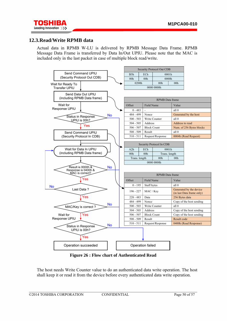
12.3. Read/Write RPMB data
Actual data in RPMB W-LU is delivered by RPMB Message Data Frame. RPMB Message Data Frame is transferred by Data In/Out UPIU. Please note that the MAC is included only in the last packet in case of multiple block read/write.
Figure 26 : Flow chart of Authenticated Read
The host needs Write Counter value to do an authenticated data write operation. The host shall keep it or read it from the device before every authenticated data write operation.
Security Protocol Out CDB
B5h ECh 0001h
00h 00h 0000h
0200h 00h 00h
0000 0000h
RPMB Data frame
Offset Field Name Value
0 - 483 - all 0
484 - 499 Nonce Generated by the host
500 - 503 Write Counter all 0
504 - 505 Address Address to read
506 - 507 Block Count Num. of 256 Bytes blocks
508 - 509 Result all 0
510 - 511 Request/Response 0004h (Read Request)
Security Protocol In CDB
A2h ECh 0001h
00h 00h Trans. length
Trans. length 00h 00h
0000 0000h
RPMB Data frame
Offset Field Name Value
0 - 195 Stuff bytes all 0
196 - 227 MAC / Key Generated by the device (in last Data frame only)
228 - 483 Data 256 Bytes data
484 - 499 Nonce Copy of the host sending
500 - 503 Write Counter all 0
504 - 505 Address Copy of the host sending
506 - 507 Block Count Copy of the host sending
508 - 509 Result Result code
510 - 511 Request/Response 0400h (Read Response)

M1PCA00-010
©2014 TOSHIBA CORPORATION CONFIDENTIAL Page 51 of 57
Figure 27 : Flow chart of Authenticated write
Command UPIU
xx00 0001b W=1, R=0 C4h Task Tag
01h 00h 00h 00h
00h 00h 00h 00h
Multiple of 512 Bytes
B5h ECh 0001h
00h 00h Trans. length
Trans. length 00h 00h
0000 0000h
Header E2ECRC (omit if HD=0)
RPMB Data frame
Offset Field Name Value
0 - 195 Stuff bytes all 0
196 - 227 MAC / Key Generated by the host (in last Data In UPIU only)
228 - 483 Data 256 Bytes data
484 - 499 Nonce all 0
500 - 503 Write Counter Current WC value
504 - 505 Address Address to write
506 - 507 Block Count Num. of 256 Bytes blocks
508 - 509 Result all 0
510 - 511 Request/Response 0003h (Write Request)
RPMB Data frame
Offset Field Name Value
0 - 509 - all 0
510 - 511 Request/Response 0005h (Result read Request)
RPMB Data frame
Offset Field Name Value
0 - 195 Stuff bytes all 0
196 - 227 MAC / Key Generated by the device
228 - 499 - all 0
500 - 503 Write Counter Incremented WC value
504 - 505 Address Copy of the host sending
506 - 507 Block Count all 0
508 - 509 Result Result code
510 - 511 Request/Response 0300h (Write Response)

M1PCA00-010
©2014 TOSHIBA CORPORATION CONFIDENTIAL Page 52 of 57
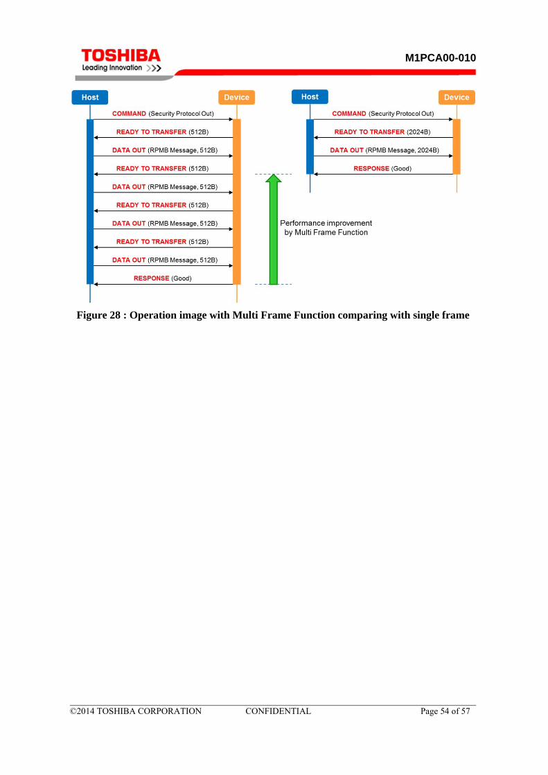
12.4. RPMB Multi Frame Function (TOSHIBA specific)
TOSHIBA UFS device supports RPMB Multi Frame data transmission as vendor specific function. In UFS standard, DATA OUT or DATA IN UPIU in RPMB data transmission is fixed to 512 bytes, but Multi Frame function enables a host to transmit more than 512 bytes data in a single DATA OUT or DATA IN UPIU. So this function can improve performance during RPMB data transmission.
The function activation and deactivation are done by Query Request UPIU with the Query Function of C2h (Vendor Specific Functions). Once Multi Frame Function is enabled, a device handles RPMB data transmission with multi frames after that. The setting of Multi Frame Function is initialized by any reset operation.
The maximum data size of RPMB is defied by bRPMB_ReadWriteSize in RPMB Unit Descriptor. In TOSHIBA UFS device, bRPMB_ReadWriteSize is 40h and it means that 64 frames are transmitted in a Security Protocol Out or Security Protocol In command.
Table 26 : Query Request UPIU and Data Frame Format for Multi Frame Function
(a) Query Request UPIU
Query Request UPIU
0 xx01 0110b
1 Flags
2 Reserved
3 Task Tag
4 Reserved
5 Query Function (C2h)
6 Reserved
7 Reserved
8 Total EHS Length
9 Reserved
10-11 Data Segment Length
12-27 Transaction Specific Fields
28-31 Reserved
Data[0]-Data[511]
(b) Data Frame Formant
Data Size Name Description
0 1 Subcommand No. 0Ah
1-3 3 Reserved
4-7 4 RPMB Multi Frame Enable password
7E87390Ch
8 1 RPMB Read / Write 00h: Read from RPMB Multi Frame Enable 01h: Write to RPMB Multi Frame Enable
9 1 RPMB Multi Frame Enable 00h: RPMB Multi Frame is disable (Default)01h: RPMB Multi Frame is enable
10-511 502 Reserved

M1PCA00-010
©2014 TOSHIBA CORPORATION CONFIDENTIAL Page 53 of 57
Table 27 : Query Response UPIU and Data Frame Format for Multi Frame Function
(a) Query Request UPIU
Query Request UPIU
0 xx11 0110b
1 Flags
2 Reserved
3 Task Tag
4 Reserved
5 Query Function (C2h)
6 Reserved
7 Reserved
8 Total EHS Length
9 Reserved
10-11 Data Segment Length
12-27 Transaction Specific Fields
28-31 Reserved
Data[0]-Data[511]
(b) Data Frame Format
Data Size Name Description
0 1 Sub command No. 0Ah
1-2 2 Reserved
3 1 Response A0h: Success E0h: Failure
4-7 4 Reserved
8 1 RPMB Read / Write 00h: Read from RPMB Multi Frame Enable 01h: Write to RPMB Multi Frame Enable
9 1 RPMB Multi Frame Enable Value of RPMB Multi Frame Enable parameter.
10-511 502 Reserved
M1PCA00-010
©2014 TOSHIBA CORPORATION CONFIDENTIAL Page 54 of 57
Figure 28 : Operation image with Multi Frame Function comparing with single frame

M1PCA00-010
©2014 TOSHIBA CORPORATION CONFIDENTIAL Page 55 of 57
13. Context and System Data Tag Management When receiving System Data Tag notification along with the write command, a device stores the system data in the System Data area. In case the capacity available for storing System Data is completely consumed, the device stores the System Data in regular storage. System Data areas are available only in Normal memory type logical units.
14. Data Scrambling Data Scrambling is a technique used to mitigate problems related to Electromagnetic Interference. Transmitted data are scrambled to reduce the possibility of repetitive pattern in the Link. To enable and disable this function, power mode change is required

M1PCA00-010
©2014 TOSHIBA CORPORATION CONFIDENTIAL Page 56 of 57
Document Revision History Rev. 0.1 Mar. 20th, 2013 Released initial revision.

M1PCA00-010
©2014 TOSHIBA CORPORATION CONFIDENTIAL Page 57 of 57
RESTRICTIONS ON PRODUCT USE TOSHIBA Corporation, and its subsidiaries and affiliates (collectively "TOSHIBA"), reserve the right to make changes to the
information in this document, and related hardware, software and systems (collectively "Product") without notice.
This document and any information herein may not be reproduced without prior written permission from TOSHIBA. Even with TOSHIBA's written permission, reproduction is permissible only if reproduction is without alteration/omission.
Though TOSHIBA works continually to improve Product's quality and reliability, Product can malfunction or fail. Customers are responsible for complying with safety standards and for providing adequate designs and safeguards for their hardware, software and systems which minimize risk and avoid situations in which a malfunction or failure of Product could cause loss of human life, bodily injury or damage to property, including data loss or corruption. Before customers use the Product, create designs including the Product, or incorporate the Product into their own applications, customers must also refer to and comply with (a) the latest versions of all relevant TOSHIBA information, including without limitation, this document, the specifications, the data sheets and application notes for Product and the precautions and conditions set forth in the "TOSHIBA Semiconductor Reliability Handbook" and (b) the instructions for the application with which the Product will be used with or for. Customers are solely responsible for all aspects of their own product design or applications, including but not limited to (a) determining the appropriateness of the use of this Product in such design or applications; (b) evaluating and determining the applicability of any information contained in this document, or in charts, diagrams, programs, algorithms, sample application circuits, or any other referenced documents; and (c) validating all operating parameters for such designs and applications. TOSHIBA ASSUMES NO LIABILITY FOR CUSTOMERS' PRODUCT DESIGN OR APPLICATIONS.
PRODUCT IS NEITHER INTENDED NOR WARRANTED FOR USE IN EQUIPMENTS OR SYSTEMS THAT REQUIRE EXTRAORDINARILY HIGH LEVELS OF QUALITY AND/OR RELIABILITY, AND/OR A MALFUNCTION OR FAILURE OF WHICH MAY CAUSE LOSS OF HUMAN LIFE, BODILY INJURY, SERIOUS PROPERTY DAMAGE AND/OR SERIOUS PUBLIC IMPACT ("UNINTENDED USE"). Except for specific applications as expressly stated in this document, Unintended Use includes, without limitation, equipment used in nuclear facilities, equipment used in the aerospace industry, medical equipment, equipment used for automobiles, trains, ships and other transportation, traffic signaling equipment, equipment used to control combustions or explosions, safety devices, elevators and escalators, devices related to electric power, and equipment used in finance-related fields. IF YOU USE PRODUCT FOR UNINTENDED USE, TOSHIBA ASSUMES NO LIABILITY FOR PRODUCT. For details, please contact your TOSHIBA sales representative.
Do not disassemble, analyze, reverse-engineer, alter, modify, translate or copy Product, whether in whole or in part.
Product shall not be used for or incorporated into any products or systems whose manufacture, use, or sale is prohibited under any applicable laws or regulations.
The information contained herein is presented only as guidance for Product use. No responsibility is assumed by TOSHIBA for any infringement of patents or any other intellectual property rights of third parties that may result from the use of Product. No license to any intellectual property right is granted by this document, whether express or implied, by estoppel or otherwise.
ABSENT A WRITTEN SIGNED AGREEMENT, EXCEPT AS PROVIDED IN THE RELEVANT TERMS AND CONDITIONS OF SALE FOR PRODUCT, AND TO THE MAXIMUM EXTENT ALLOWABLE BY LAW, TOSHIBA (1) ASSUMES NO LIABILITY WHATSOEVER, INCLUDING WITHOUT LIMITATION, INDIRECT, CONSEQUENTIAL, SPECIAL, OR INCIDENTAL DAMAGES OR LOSS, INCLUDING WITHOUT LIMITATION, LOSS OF PROFITS, LOSS OF OPPORTUNITIES, BUSINESS INTERRUPTION AND LOSS OF DATA, AND (2) DISCLAIMS ANY AND ALL EXPRESS OR IMPLIED WARRANTIES AND CONDITIONS RELATED TO SALE, USE OF PRODUCT, OR INFORMATION, INCLUDING WARRANTIES OR CONDITIONS OF MERCHANTABILITY, FITNESS FOR A PARTICULAR PURPOSE, ACCURACY OF INFORMATION, OR NONINFRINGEMENT.
Do not use or otherwise make available Product or related software or technology for any military purposes, including without limitation, for the design, development, use, stockpiling or manufacturing of nuclear, chemical, or biological weapons or missile technology products (mass destruction weapons). Product and related software and technology may be controlled under the applicable export laws and regulations including, without limitation, the Japanese Foreign Exchange and Foreign Trade Law and the U.S. Export Administration Regulations. Export and re-export of Product or related software or technology are strictly prohibited except in compliance with all applicable export laws and regulations.
Please contact your TOSHIBA sales representative for details as to environmental matters such as the RoHS compatibility of Product. Please use Product in compliance with all applicable laws and regulations that regulate the inclusion or use of controlled substances, including without limitation, the EU RoHS Directive. TOSHIBA ASSUMES NO LIABILITY FOR DAMAGES OR LOSSES OCCURRING AS A RESULT OF NONCOMPLIANCE WITH APPLICABLE LAWS AND REGULATIONS.