Application Note rev1.3 - Electronics & Appliances: … is no waste of electrical printed circuit...
66
Application Note rev1.3.2 LH934A (HV-AC) Samsung Electronics
Transcript of Application Note rev1.3 - Electronics & Appliances: … is no waste of electrical printed circuit...
Application Note rev1.3.2
LH934A (HV-AC)
Samsung Electronics

IndexIndex1. Introduction Page
1 1 System Overview1.1 System Overview
1.1.1 Product Description 4
1.1.2 Benefit and Features 5
1.2 Application 6
1.3 Package Information
1.3.1 Dimension and Pad Configuration 7
1.3.1 Absolute Maximum Rating 8
2. Warnings 9
3. Basic AC Operation
3.1 Incandescent Edition Lamp Concept for LED 10
3.2 Normal AC Operation 11
3.3 Advanced AC Operation 12
3.4 AC vs DC Operation 13
4. Product & Technology Description
4.1 Optical Considerationp
4.1.1 Chromaticity Bins 14
4.1.2 Product Code 15
4.1.3 Chromaticity Coordinates 16
4.1.4 Luminous Flux 22
4 1 5 Spectrum 234.1.5 Spectrum 23
4.1.6 Polar Intensity Diagram 24
4.1.7 Coordinate variation test 25
4.1.8 Characteristic Properties 26
4.1.9 Operating properties vs Solder Temperature 27
2
4.2 Electrical Considerations
4.2.1 Forward Voltage and Reverse Voltage 28
4.2.2 100~120Vac vs 220~240Vac driving method 29
4.2.3 Driving method 30
4.2.4 summary of each driving method 31
4.2.5 Resistor Value Table & Properties 32
4.2.6 Resistor Value and P.T.C Table & Properties 36
4 2 7 C i V l T bl & P i 404.2.7 Capacitor Value Table & Properties 40
4.2.8 Parallel Capacitor and Resistor Values 44
4.2.9 Capacitor Value Table & Properties 46
4.3 Mechanical Considerations
4.3.1 Mechanical Drawing 48
4.3.2 SMT set 49
4.3.3 Reflow Profile 51
4.4 Thermal Considerations
4.4.1 Thermal Resistance 52
5. Dimming Guide
5.1 Dimming
5.1.1 Recommended Lutron Dimmer 53
5.1.2 Unmatched dimmer for triac operation 54
6. Safety
6 1 UL cUL 556.1 UL, cUL 55
6.2 CE, VDE 56
6.3 Eye safety, MMC 57
6.4 RoHS, Hazard Substance Analysis 59
7. Application
7 1 A li bl fi ld 617.1 Applicable field 61
7.2 Design guide 62
7.3 2nd Lens solution 64
8. Revision History 66
3

1.1 System Overview
1.1.1 Product Description
• HV‐AC Product is directly connected to AC power source
without any AC/DC convertery
• Rectifier function merged in single bidirectional AC‐LED die
• Unique monolithic LED die technology adopted
• Robust design : EMI/EMC, Surge, ESD
• High electrical performance : PF, THD*
• Available in various Voltage ranges:
100~120Vac, 220~240Vac, 277Vac
• 100~120Hz current driving at AC source 50~60Hz
• Long life span and high reliability
• Available in white (2700K to 6500K CCT)
• Dimmable**
• Excellent color reproduction
• Eco‐friendly light
4
* PF (Power Factor), THD(Total Harmonic Distortion)
** low voltage dimmer is suitable . See page. 4

1.1 System Overview
1.1.2 Benefits and Features
• Simple Design:
Just connect infinitely parallel circuit connections without the
trouble of making LED Arrays such as with DC LEDs.
• Compact Size & Low Weight:
User can get space & weight saving in the fixture
by eliminating the power supply unit.
• Longer System Life‐time:
Lighting Life‐time of the fixture can be equivalent to the LED
long life‐ time rather than relatively short power supply life‐
time.
• Low Cost solution:
U t b fit f i l d i tUser can get benefits of saving power supply device cost.
• Eco friendly solution:
There is no waste of electrical printed circuit board. etc.
• Wide operation range:
5
Wide operation range:
Driving package power consumption range is 3.3W ~ 4.5W
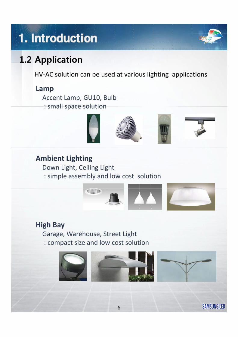
1.2 Application
LampAccent Lamp, GU10, Bulb: small space solution
HV‐AC solution can be used at various lighting applications
: small space solution
Ambient LightingDown Light, Ceiling Light: simple assembly and low cost solution
High BayGarage, Warehouse, Street Light: compact size and low cost solution
6

1.3 Package Information
1.3.1 Dimension and Pad Configuration• Symmetric package with 4 electrical pads and 1 thermal pad
• 4 electrical pads are bi‐polarity and 2‐pair string (①‐②, ④‐⑤)
• 1 thermal pad(③) is non‐polarity
Top View
Bottom View
Pad Function
① Bi-polarity
② Bi-polarity
③Thermal
Non-polarity(Electrically Isolated)
Dimension (12.4x11.4x4.38)
7
(Electrically Isolated)
④ Bi-polarity
⑤ Bi-polarity
LED Electrical Circuit
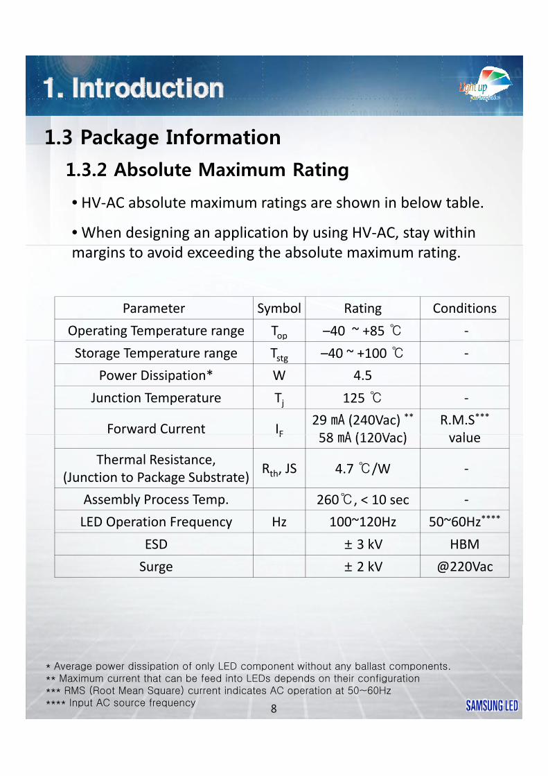
1.3 Package Information
1.3.2 Absolute Maximum Rating
• HV‐AC absolute maximum ratings are shown in below table.
• When designing an application by using HV‐AC, stay within
Parameter Symbol Rating Conditions
Operating Temperature range Top –40 ~ +85 ‐
margins to avoid exceeding the absolute maximum rating.
Storage Temperature range Tstg –40 ~ +100 ‐
Power Dissipation* W 4.5
Junction Temperature Tj 125 ‐
Forward Current IF29 (240Vac) **
58 (120V )R.M.S***
lF 58 (120Vac) value
Thermal Resistance, (Junction to Package Substrate)
Rth, JS 4.7 /W ‐
Assembly Process Temp. 260, < 10 sec ‐
LED Operation Frequency Hz 100~120Hz 50~60Hz****
ESD ± 3 kV HBM
Surge ± 2 kV @220Vac
8
* Average power dissipation of only LED component without any ballast components.** Maximum current that can be feed into LEDs depends on their configuration*** RMS (Root Mean Square) current indicates AC operation at 50~60Hz**** Input AC source frequency

2.1 Warnings1) For avoiding over-current, customers are recommended to apply resistors to
prevent sudden change of the input current caused by slight shift of the voltage.
2) This device should not be used in any type of fluid such as water, oil, organicsolvent, etc. If decontamination is required, IPA could be recommended to use.
3) Wh LED ill i t ti t h ld b d id d ft id i th3) When LEDs illuminate, operating current should be decided after considering the ambient maximum temperature(Refer to the maximum rating table).
4) LEDs must be stored in a clean environment.If the LEDs are to be stored for 3 months or more after being shipped from S LED, they should be packed in a container sealed with nitrogen gas. (Shelf life of sealed bags: 12 months, temp. 0~40 , 20~70 % RH)
5) After bag is opened, device subjected to soldering, solder reflow, or otherhigh temperature processes must be:a. Mounted within 168 hours (7 days) at an assembly line with a condition of no more than 30 /60 %RH,
b. Stored at <10 %RH.
6) Repack unused products with anti-moisture pack seal pack to close any opening6) Repack unused products with anti moisture pack, seal pack to close any opening and then store in a dry place.
7) Devices require baking before mounting, if humidity card reading is >60 % at 23±5 .
8) If baking is required, devices must be baked for 24 hours at 65±5 .
9) The LEDs are sensitive to static electricity and surge current. It is recommended to use a wrist band or anti-electrostatic glove when handling the LEDs.
If voltage exceeding the absolute maximum rating is applied to LEDs, it may cause damage or even destruction of LED devices.
Damaged LEDs may show some unusual characteristics such as increase in leak
9
g ycurrent, lowered turn-on voltage, or abnormal lighting of LEDs at low current.

3.1 Incandescent Edison Lamp Concept for LED •AC LED is modeled after the incandescent Edison bulb
Filament AC LED DC LED
※Without PFC circuit
* AC Voltage Waves / Current Waves
[Edison Bulb] [AC‐LED] [Normal DC Operation]
• Difference in lighting properties noticed by the human eye is small
• Incandescent lamps emit their• Incandescent lamps emit their luminous output differently as input voltage sweep and AC‐LED also has similar properties
10
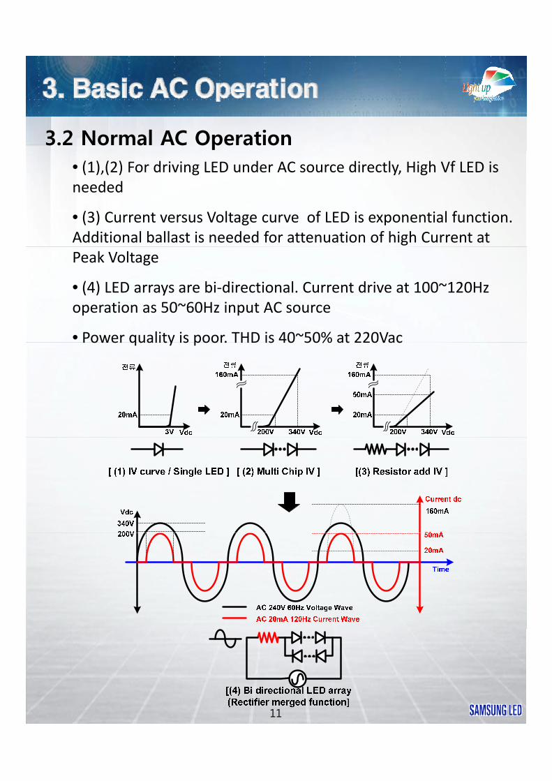
3.2 Normal AC Operation• (1),(2) For driving LED under AC source directly, High Vf LED is needed
• (3) Current versus Voltage curve of LED is exponential function. Additional ballast is needed for attenuation of high Current at Peak Voltage
• (4) LED arrays are bi‐directional. Current drive at 100~120Hz operation as 50~60Hz input AC source
• Power quality is poor. THD is 40~50% at 220VacPower quality is poor. THD is 40 50% at 220Vac
11

3.3 Advanced AC Operation• The purpose of improving AC solution is to make narrow phase difference between Voltage and Current. Normal AC operation is very simple but has poor power quality and low flickering performance – turn on duty ratio (Ton/T) is 50~60%
• Some kind of solution like a switching logic controller could reduce phase difference and finally get advanced quality – THD, PFC, turn‐on duty ratio(Ton/T) is about 80% which reduces flicker
• Complicated control system is not desirable for AC solution
[Normal AC Operation]
12
[Advanced AC Operation]
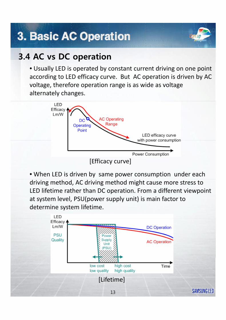
3.4 AC vs DC operation• Usually LED is operated by constant current driving on one point according to LED efficacy curve. But AC operation is driven by AC voltage, therefore operation range is as wide as voltage alternately changes.
• When LED is driven by same power consumption under each
[Efficacy curve]
driving method, AC driving method might cause more stress to LED lifetime rather than DC operation. From a different viewpoint at system level, PSU(power supply unit) is main factor to determine system lifetime.
13
[Lifetime]
4.1 Optical Considerations
4.1.1 Chromaticity Bins
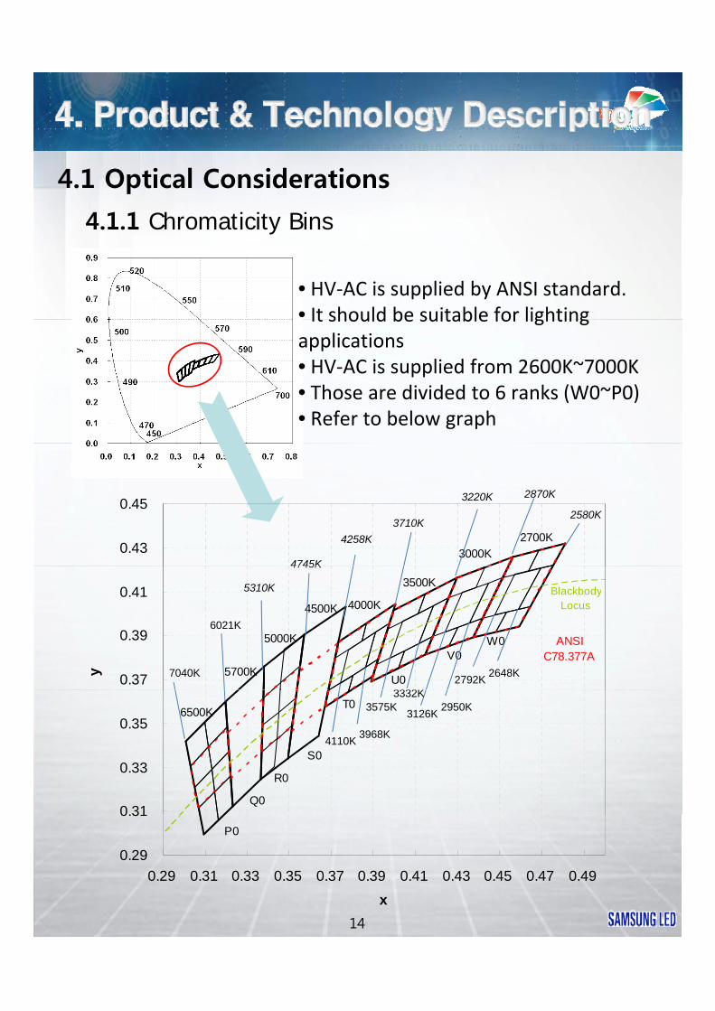
• HV‐AC is supplied by ANSI standard.• It should be suitable for lightingIt should be suitable for lighting applications• HV‐AC is supplied from 2600K~7000K• Those are divided to 6 ranks (W0~P0)• Refer to below graph
0.43
0.45
3000K2700K
4745K
4258K
3710K2580K
3220K 2870K
0.37
0.39
0.41
y
U0
V0W0
5700K
5000K
4500K 4000K
3500K
ANSIC78.377A
BlackbodyLocus
5310K
4745K
2792K2648K
3332K
7040K
6021K
0 31
0.33
0.35
R0
T0
Q0
S0
6500K 3126K2950K3575K
3332K
4110K3968K
14
0.29
0.31
0.29 0.31 0.33 0.35 0.37 0.39 0.41 0.43 0.45 0.47 0.49
x
P0
4.1 Optical Considerations
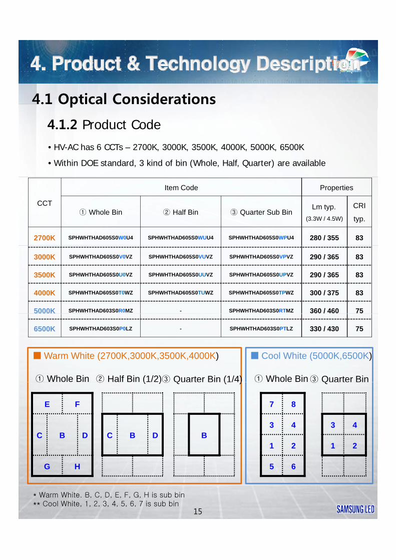
4.1.2 Product Code
• HV-AC has 6 CCTs – 2700K, 3000K, 3500K, 4000K, 5000K, 6500K
• Within DOE standard, 3 kind of bin (Whole, Half, Quarter) are available
CCT
Item Code Properties
① Whole Bin ② Half Bin ③ Quarter Sub BinLm typ.
(3.3W / 4.5W)
CRI
typ.
2700K SPHWHTHAD605S0W0U4 SPHWHTHAD605S0WUU4 SPHWHTHAD605S0WPU4 280 / 355 83
3000K SPHWHTHAD605S0V0VZ SPHWHTHAD605S0VUVZ SPHWHTHAD605S0VPVZ 290 / 365 83
3500K SPHWHTHAD605S0U0VZ SPHWHTHAD605S0UUVZ SPHWHTHAD605S0UPVZ 290 / 365 83
4000K SPHWHTHAD605S0T0WZ SPHWHTHAD605S0TUWZ SPHWHTHAD605S0TPWZ 300 / 375 83
5000K SPHWHTHAD603S0R0MZ - SPHWHTHAD603S0RTMZ 360 / 460 75
Cool White (5000K,6500K)
① Whole Bin ② Half Bin (1/2)③ Quarter Bin (1/4)
6500K SPHWHTHAD603S0P0LZ - SPHWHTHAD603S0PTLZ 330 / 430 75
Warm White (2700K,3000K,3500K,4000K)
① Whole Bin③ Quarter Bin
E F
C B D
7 8
3 4
1 2
① ② ( )③ Qua e ( / )
C B D B
① ③ Qua e
3 4
1 2
15
G H 5 6
* Warm White. B, C, D, E, F, G, H is sub bin** Cool White, 1, 2, 3, 4, 5, 6, 7 is sub bin

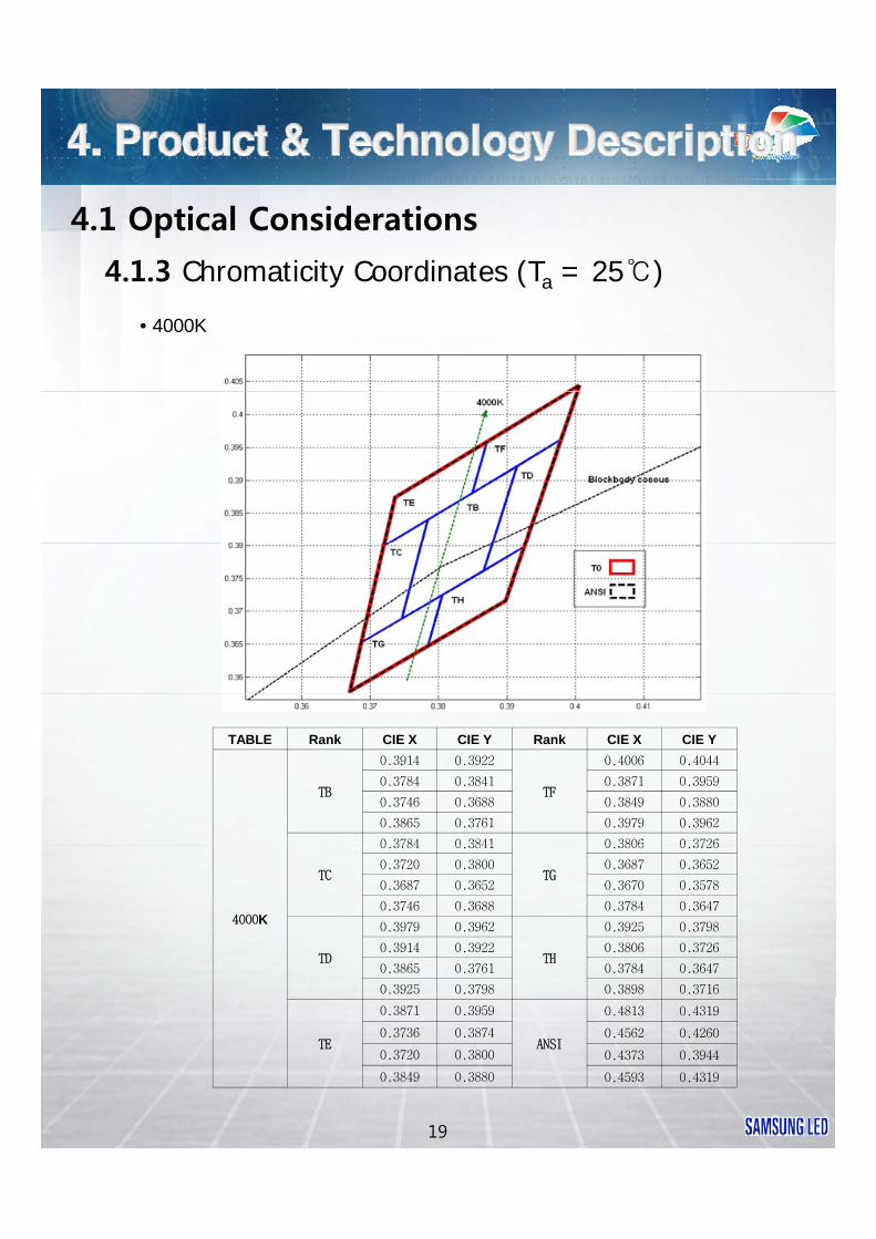
4.1 Optical Considerations
4.1.3 Chromaticity Coordinates (Ta = 25)
• 2700K
TABLE Rank CIE X CIE Y Rank CIE X CIE Y
WB
0.4697 0.4211
WF
0.4813 0.4319
0.4576 0.4183 0.4688 0.4290
0.4477 0.3998 0.4636 0.4196
0.4591 0.4024 0.4758 0.4225
0 4576 0 4183 0 4534 0 4012
2700K
WC
0.4576 0.4183
WG
0.4534 0.4012
0.4515 0.4168 0.4420 0.3985
0.4420 0.3985 0.4373 0.3893
0.4477 0.3998 0.4483 0.3919
WD
0.4758 0.4225
WH
0.4648 0.4038
0.4697 0.4211 0.4534 0.4012
0.4591 0.4024 0.4483 0.3919
16
0.4648 0.4038 0.4593 0.3944
WE
0.4688 0.4290
ANSI
0.4813 0.4319
0.4562 0.4260 0.4562 0.4260
0.4515 0.4168 0.4373 0.3944
0.4636 0.4196 0.4593 0.4319

4.1 Optical Considerations
4.1.3 Chromaticity Coordinates (Ta = 25)
• 3000K
TABLE Rank CIE X CIE Y Rank CIE X CIE Y
VB
0.4451 0.4146
VF
0.4562 0.4260
0.4324 0.4100 0.4431 0.4213
0.4244 0.3922 0.4388 0.4122
0.4361 0.3964 0.4515 0.4168
0 4324 0 4100 0 4303 0 3944
3000K
VC
0.4324 0.4100
VG
0.4303 0.3944
0.4261 0.4077 0.4185 0.3902
0.4185 0.3902 0.4147 0.3814
0.4244 0.3922 0.4260 0.3854
VD
0.4515 0.4168
VH
0.4420 0.3985
0.4451 0.4146 0.4303 0.3944
0.4361 0.3964 0.4260 0.3854
17
0.4420 0.3985 0.4373 0.3893
VE
0.4431 0.4213
ANSI
0.4813 0.4319
0.4299 0.4165 0.4562 0.4260
0.4261 0.4077 0.4373 0.3893
0.4388 0.4122 0.4593 0.3944

4.1 Optical Considerations
4.1.3 Chromaticity Coordinates (Ta = 25)
• 3500K
TABLE Rank CIE X CIE Y Rank CIE X CIE Y
UB
0.4188 0.4042
UF
0.4299 0.4165
0.4042 0.3970 0.4148 0.4090
0.3983 0.3803 0.4115 0.4005
0.4118 0.3869 0.4261 0.4077
0 4042 0 3970 0 4050 0 3837
3500K
UC
0.4042 0.3970
UG
0.4050 0.3837
0.3969 0.3934 0.3916 0.3771
0.3916 0.3771 0.3889 0.3690
0.3983 0.3803 0.4018 0.3752
UD
0.4261 0.4077
UH
0.4185 0.3902
0.4188 0.4042 0.4050 0.3837
0.4118 0.3869 0.4018 0.3752
0 4185 0 3902 0 4147 0 3814
18
0.4185 0.3902 0.4147 0.3814
UE
0.4148 0.4090
ANSI
0.4813 0.4319
0.3996 0.4015 0.4562 0.4260
0.3969 0.3934 0.4373 0.3944
0.4115 0.4005 0.4593 0.4319
4.1 Optical Considerations
4.1.3 Chromaticity Coordinates (Ta = 25)
• 4000K
TABLE Rank CIE X CIE Y Rank CIE X CIE Y
TB
0.3914 0.3922
TF
0.4006 0.4044
0.3784 0.3841 0.3871 0.3959
0.3746 0.3688 0.3849 0.3880
0.3865 0.3761 0.3979 0.3962
0 3784 0 3841 0 3806 0 3726
4000K
TC
0.3784 0.3841
TG
0.3806 0.3726
0.3720 0.3800 0.3687 0.3652
0.3687 0.3652 0.3670 0.3578
0.3746 0.3688 0.3784 0.3647
TD
0.3979 0.3962
TH
0.3925 0.3798
0.3914 0.3922 0.3806 0.3726
0.3865 0.3761 0.3784 0.3647
0.3925 0.3798 0.3898 0.3716
19
TE
0.3871 0.3959
ANSI
0.4813 0.4319
0.3736 0.3874 0.4562 0.4260
0.3720 0.3800 0.4373 0.3944
0.3849 0.3880 0.4593 0.4319
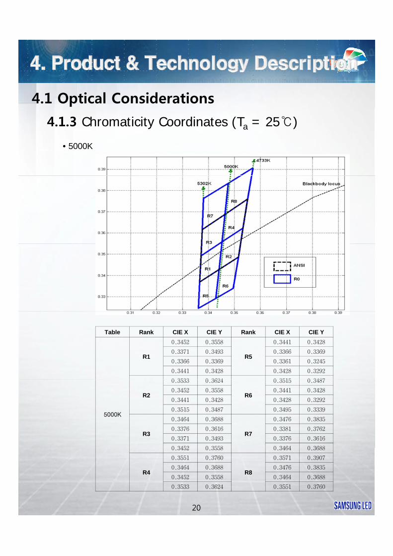
4.1 Optical Considerations
4.1.3 Chromaticity Coordinates (Ta = 25)
• 5000K
Table Rank CIE X CIE Y Rank CIE X CIE Y
R1
0.3452 0.3558
R5
0.3441 0.3428
0.3371 0.3493 0.3366 0.3369
0.3366 0.3369 0.3361 0.3245
0.3441 0.3428 0.3428 0.3292
0 3533 0 3624 0 3515 0 3487
5000K
R2
0.3533 0.3624
R6
0.3515 0.3487
0.3452 0.3558 0.3441 0.3428
0.3441 0.3428 0.3428 0.3292
0.3515 0.3487 0.3495 0.3339
R3
0.3464 0.3688
R7
0.3476 0.3835
0.3376 0.3616 0.3381 0.3762
0.3371 0.3493 0.3376 0.3616
0 3452 0 3558 0 3464 0 3688
20
0.3452 0.3558 0.3464 0.3688
R4
0.3551 0.3760
R8
0.3571 0.3907
0.3464 0.3688 0.3476 0.3835
0.3452 0.3558 0.3464 0.3688
0.3533 0.3624 0.3551 0.3760
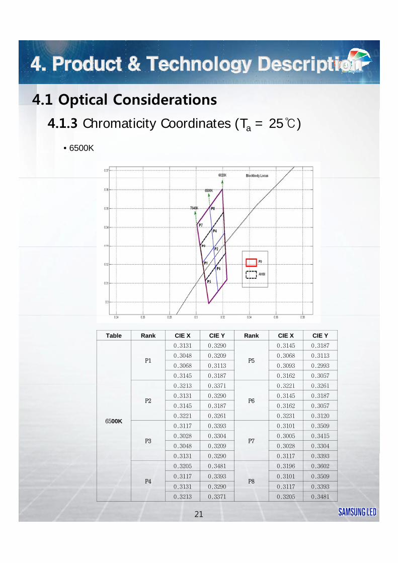
4.1 Optical Considerations
4.1.3 Chromaticity Coordinates (Ta = 25)
• 6500K
Table Rank CIE X CIE Y Rank CIE X CIE Y
P1
0.3131 0.3290
P5
0.3145 0.3187
0.3048 0.3209 0.3068 0.3113
0.3068 0.3113 0.3093 0.2993
0.3145 0.3187 0.3162 0.3057
0 3213 0 3371 0 3221 0 3261
6500K
P2
0.3213 0.3371
P6
0.3221 0.3261
0.3131 0.3290 0.3145 0.3187
0.3145 0.3187 0.3162 0.3057
0.3221 0.3261 0.3231 0.3120
P3
0.3117 0.3393
P7
0.3101 0.3509
0.3028 0.3304 0.3005 0.3415
0.3048 0.3209 0.3028 0.3304
21
0.3131 0.3290 0.3117 0.3393
P4
0.3205 0.3481
P8
0.3196 0.3602
0.3117 0.3393 0.3101 0.3509
0.3131 0.3290 0.3117 0.3393
0.3213 0.3371 0.3205 0.3481

4.1 Optical Considerations
4.1.4 Luminous Flux (Ta = 25)
2700K(83Ra)
3.3W*22mA(rms) / 220Vac44mA(rms) / 110Vac
4.5W**29mA(rms) / 220Vac58mA(rms) / 110Vac
Min. Typ. Max. Min. Typ. Max.
3000K(83Ra)
3.3W22mA(rms) / 220Vac44mA(rms) / 110Vac
4.5W22mA(rms) / 220Vac44mA(rms) / 110Vac
Min. Typ. Max. Min. Typ. Max.yp yp
U4
U1 220 - 240 275 - 300
V1 240 - 260 300 - 330
W1 260 - 280 330 - 355
X1 280 - 300 355 - -
yp yp
VZ
V1 240 - 260 285 - 310
W1 260 - 280 310 - 340
X1 280 - 300 340 - 365
01 300 - - 365 - -
3500K(83Ra)
3.3W22mA(rms) / 220Vac44mA(rms) / 110Vac
4.5W22mA(rms) / 220Vac44mA(rms) / 110Vac
Min. Typ. Max. Min. Typ. Max.
VZ
V1 240 - 260 285 - 310
W1 260 - 280 310 - 340
4000K(83Ra)
3.3W22mA(rms) / 220Vac44mA(rms) / 110Vac
4.5W22mA(rms) / 220Vac44mA(rms) / 110Vac
Min. Typ. Max. Min. Typ. Max.
WZ
W1 260 - 280 310 - 340
X1 280 - 300 340 - 365VZ
X1 280 - 300 340 - 365
01 300 - - 365 - -
WZ01 300 - 320 365 - 390
11 320 - - 390 - -
5000K(75Ra)
3.3W22mA(rms) / 220Vac44mA(rms) / 110Vac
4.5W22mA(rms) / 220Vac44mA(rms) / 110Vac
6500K(75Ra)
3.3W22mA(rms) / 220Vac44mA(rms) / 110Vac
4.5W22mA(rms) / 220Vac44mA(rms) / 110Vac
(75Ra)Min. Typ. Max. Min. Typ. Max.
MZ
M1 280 - 310 355 - 395
N1 310 - 340 395 - 435
P1 340 - 370 435 - 470
Q1 370 - - 470 - -
(75Ra)Min. Typ. Max. Min. Typ. Max.
LZ
L1 250 - 280 315 - 355
M1 280 - 310 355 - 395
N1 310 - 340 395 - 435
P1 340 - - 435 -
22
※ Tolerance : ±10%* Reference binning is done @ IF=22mA(rms), 3.3W.** Luminous flux at 4.5W operation is provided by statistical correlation with luminous flux
at 3.3W operation.
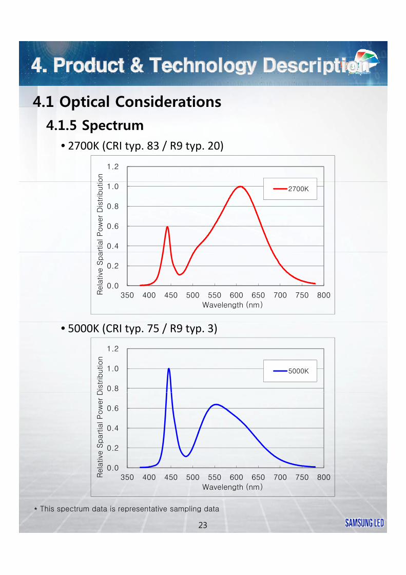
4.1 Optical Considerations
4.1.5 Spectrum• 2700K (CRI typ. 83 / R9 typ. 20)
1.2
on
0.4
0.6
0.8
1.0
artia
l Pow
er D
istrib
utio
2700K
0.0
0.2
350 400 450 500 550 600 650 700 750 800Rela
tive
Spa
Wavelength (nm)
• 5000K (CRI typ. 75 / R9 typ. 3)
0.8
1.0
1.2
Dis
trib
ution
5000K
0.2
0.4
0.6
ative
Spartia
lPow
er D
23
* This spectrum data is representative sampling data
0.0 350 400 450 500 550 600 650 700 750 800R
ela
Wavelength (nm)

4.1 Optical Considerations
4.1.6 Polar Intensity Diagram • HV‐AC beam angle is 136° (FWHM).
1 26
[Measured Viewing Angle]
1.26mm
5.19mm
5 39mm
3.61mm
5.39mm
24
[Alignment]
* View Angle describes the spatial intensity distribution and is the difference between the angles corresponding to 50% of the maximum intensity. (Full Width Half Maximum)
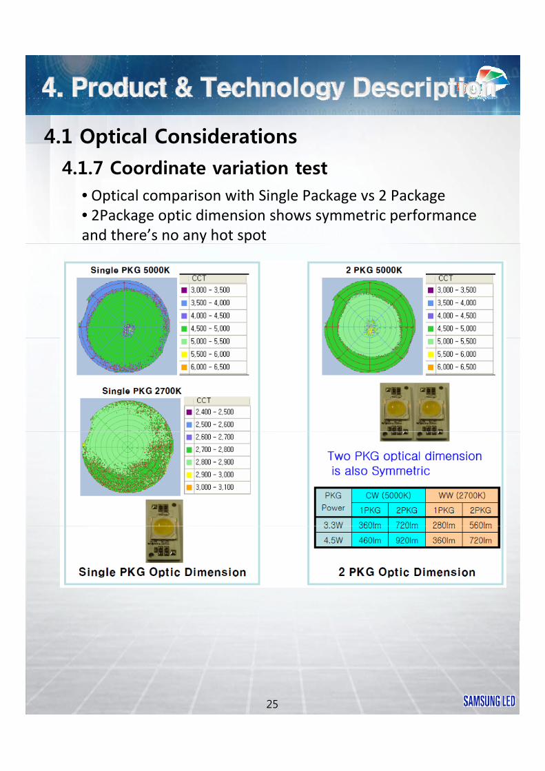
4.1 Optical Considerations
4.1.7 Coordinate variation test• Optical comparison with Single Package vs 2 Package• 2Package optic dimension shows symmetric performanceand there’s no any hot spot
25
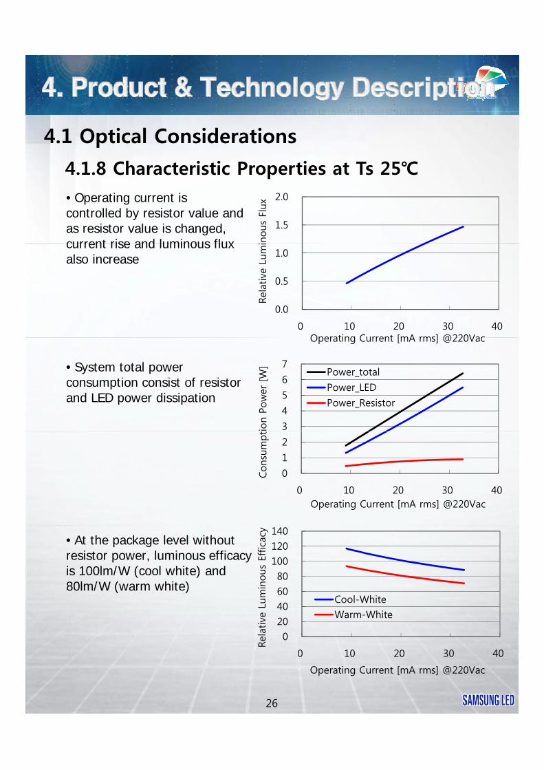
4.1 Optical Considerations
• Operating current is controlled by resistor value and as resistor value is changed, current rise and luminous flux
4.1.8 Characteristic Properties at Ts 25
1.5
2.0
nous
Flu
x
current rise and luminous flux also increase
0.0
0.5
1.0
0 10 20 30 40
Rel
ativ
e Lu
mi
Operating Current [mA rms] @220VacOperating Current [mA rms] @220Vac
3
4
5
6
7
ion
Pow
er [W
]
Power_total
Power_LED
Power_Resistor
• System total power consumption consist of resistor and LED power dissipation
0
1
2
0 10 20 30 40
Cons
umpt
Operating Current [mA rms] @220Vac
20
40
60
80
100
120
140
ve L
umin
ous
Effic
acy
Cool-White
Warm-White
• At the package level without resistor power, luminous efficacy is 100lm/W (cool white) and 80lm/W (warm white)
26
0
20
0 10 20 30 40
Rel
ativ
Operating Current [mA rms] @220Vac
4.1 Optical Considerations
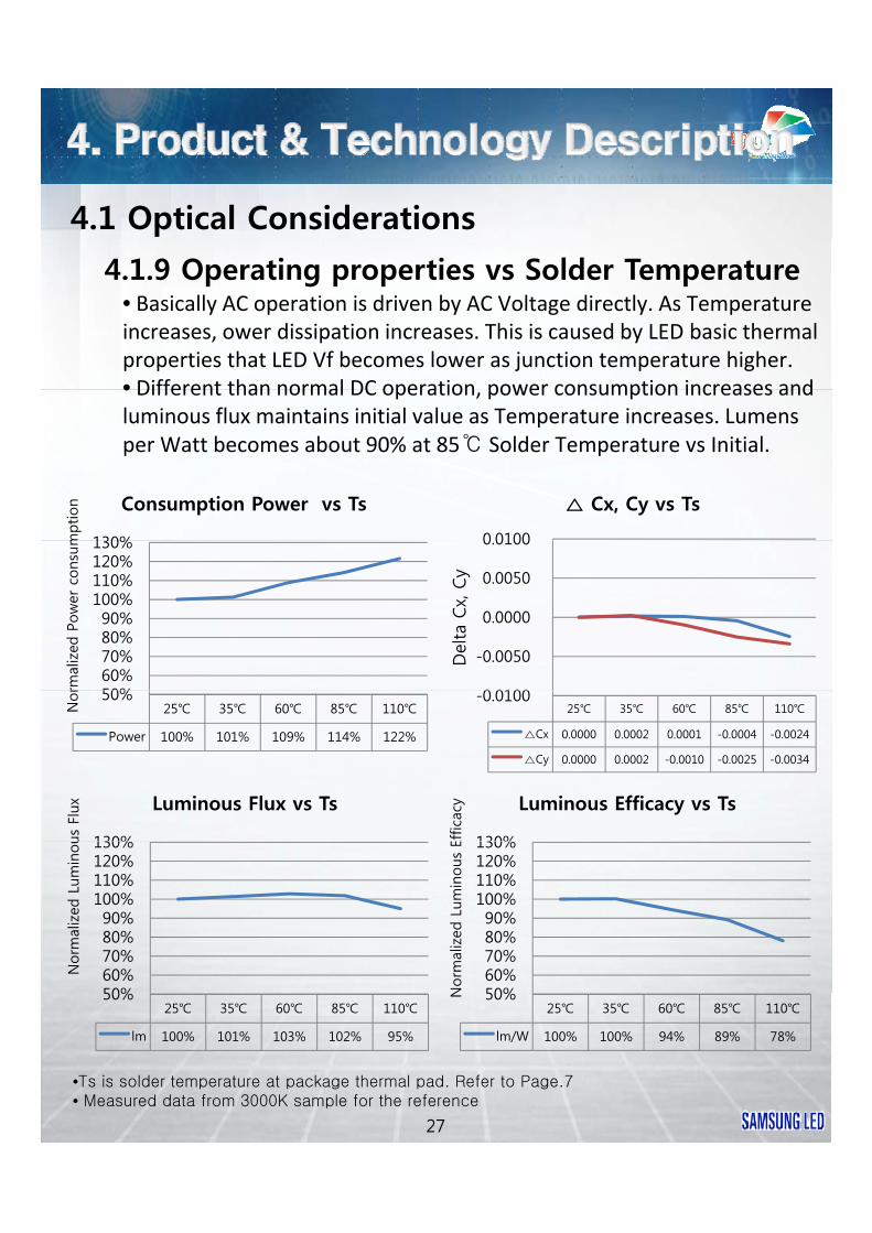
4.1.9 Operating properties vs Solder Temperature• Basically AC operation is driven by AC Voltage directly. As Temperatureincreases, ower dissipation increases. This is caused by LED basic thermal properties that LED Vf becomes lower as junction temperature higher.• Different than normal DC operation power consumption increases and• Different than normal DC operation, power consumption increases and luminous flux maintains initial value as Temperature increases. Lumens per Watt becomes about 90% at 85 Solder Temperature vs Initial.
130%mption Consumption Power vs Ts
0 0100
Cx, Cy vs Ts
50%60%70%80%90%
100%110%120%130%
rmal
ized
Pow
er c
ons
um
0 0100
-0.0050
0.0000
0.0050
0.0100
Del
ta C
x, C
y
25 35 60 85 110
Power 100% 101% 109% 114% 122%
50%
Nor
130%us F
lux Luminous Flux vs Ts
130%Effic
acy Luminous Efficacy vs Ts
25 35 60 85 110
Cx 0.0000 0.0002 0.0001 -0.0004 -0.0024
Cy 0.0000 0.0002 -0.0010 -0.0025 -0.0034
-0.0100
50%60%70%80%90%
100%110%120%130%
Norm
aliz
ed L
umin
ou
50%60%70%80%90%
100%110%120%130%
Norm
aliz
ed L
umin
ous
E
27
25 35 60 85 110
lm 100% 101% 103% 102% 95%
50%25 35 60 85 110
lm/W 100% 100% 94% 89% 78%
50%N
•Ts is solder temperature at package thermal pad. Refer to Page.7• Measured data from 3000K sample for the reference

4.2 Electrical Considerations
4.2.1 Forward Voltage and Reverse Voltage• The LED is directly connected with a test source without any additional components at measurement. LED is biased by the test source of i id l 60H (22 A ) dsinusoidal current waves at 60Hz (22mA rms), and test circuit condition is series connected circuit which Vf is measured in RMS. There’s 3 step Vf bin ‐ F1, F3, F5.
• Vf of HV‐AC LED is defined by constant sinusoidal
Symbol Condition Rank Min. Typ. Max. Unit
Vf of HV AC LED is defined by constant sinusoidal current bias, and LED die is driven by bi‐directional operation. Thus there is no reverse voltage concept.
※ Tolerance : ±5V
Vf IF = 22mA(rms) S0
F1 185 - 195Vac
(rms)F3 195 - 200
F5 200 - 205
• Actually real driving current is different with sinusoidal waves As LED has a Vf at the lowsinusoidal waves. As LED has a Vf, at the low input voltage, there’s no current flows and the shape of wave also changes.
28

4.2 Electrical Considerations
4.2.2 100~120Vac vs 220~240Vac driving method• HV‐AC product is a single package type and common use is for 110Vac & 220Vac. HV‐AC is designed for most of the input voltage ranges . Different pattern design of PCB will allow for use at 110Vac d 220Vand 220Vac.
• HV‐AC has 4 die and 2string array in single package. User can connect two electrical node at each side, then Vf becomes half of whole Vfsuitable for 100~110Vac. And If user connect just only one side electrical node, then Vf becomes whole Vf suitable for 220~240Vac.
[220Vac – Series][110Vac – Parallel]
Half of Vf Whole Vf
Schematic DiagramSchematic Diagram
29
PCB Board S.M.TPCB Board S.M.T

4.2 Electrical Considerations
4.2.3 Driving method of HV-AC
• R (Resistor Load) Most simple driving solution. Adjustable to small space application – candle, mini‐lamp
• R+PTC (Resistor + PTC Load)To limit current overflow, PTC(positive temperature coefficient) could be added in a row line with resistor
• RC (Capacitor Load)
row line with resistor
To maximize power dissipation efficiency, capacitor load recommendable for ballast. Resistor could be added in order to increase
• RC Parallel (Resistor Capacitor Parallel Load 100/120Vac)
Resistor could be added in order to increase power quality
To get high quality of power(THD under 30% & PFC over 0.9), capacitor and resistor act as
• RC Switch (Resistor Capacitor Switch Load 220/230Vac)
), pseparate ballast. Most suitable to Bulb, Down Light, Outdoor in 120Vac market
To get high quality of power(THD under 30% &
30
g g q y p (PFC over 0.9), capacitor act as switch ballast. Most suitable to Bulb, Down Light, Outdoor in 220~230Vac market

4.2 Electrical Considerations
4.2.4 Summary of each driving method
As you drive differently, it
Driving Method
1 2 3 4 5yshows different properties with same PKG!!!
PKG property ;
R R+PTC RC RCparallel
RCswitch
p p y ;3000K 4.5W(PKG)
220Vac, 120Vac
Input Voltage[Vac] 120 220 120 220 120 220 120 220
P.F.C 0.92 0.9 0.92 0.91 0.78 0.79 0.91 0.95
Elec
tric
al T.H.D [%] 40 43 38 42 46 50 27 25
Power [W]@Module 6.25 5.58 5.55 5.52 5.29 5.13 5.61 5.49
Power [W]@PKG 4.61 4.47 - - 4.48 4.59 - -
Power 80 8 90Power Efficiency [%] 74 80 - - 85 90 - -
Optic
al
LuminousFlux Ratio 417 400 345 352 385 385 409 374
Efficacy [lm/W]@Module 66.7 71.7 62.1 63.7 72.8 75 73 68
Efficacy [lm/W] 90 5 89 5 85 9 83 8
31
y@PKG 90.5 89.5 - - 85.9 83.8 - -
Feature Simple Temperature compensation High efficacy
High powerquality
High powerquality
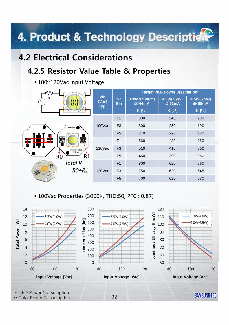
4.2 Electrical Considerations
4.2.5 Resistor Value Table & Properties
Vin(Vac)
VfBi
Target PKG Power Dissipation*
3.3W *(4.0W**)@ 44 A
4.0W(4.9W)@ 53 A
4.5W(5.5W)@ 58 A
• 100~120Vac Input Voltage
(Vac)Typ.
Bin @ 44mA @ 53mA @ 58mA
R [Ω] R [Ω] R [Ω]
100Vac
F1 330 240 200
F3 300 230 190
F5 270 220 180
F1 560 430 360 R R R R
110Vac F3 510 410 360
F5 460 390 360
120Vac
F1 800 620 560
F3 750 620 545
F5 700 620 530
R0 R1Total R = R0+R1
• 100Vac Properties (3000K, THD:50, PFC : 0.87)
12
14
W]
3.3W(4.0W) 110
120
m/W
]
3.3W(4.0W)
4 0W(4 9W)600
700
800
m] 3.3W(4.0W)
0
2
4
6
8
10
Tota
l_Pow
er [W 4.0W(4.9W)
50
60
70
80
90
100
Lum
inous
Effica
cy [
lm 4.0W(4.9W)
0
100
200
300
400
500
600
Lum
inous
Flux
[lm 4.0W(4.9W)
32* LED Power Consumption** Total Power Consumption
0
80 100 120
Input Voltage [Vac]
50
80 100 120
Input Voltage [Vac]
0
80 100 120
Input Voltage [Vac]
4.2 Electrical Considerations
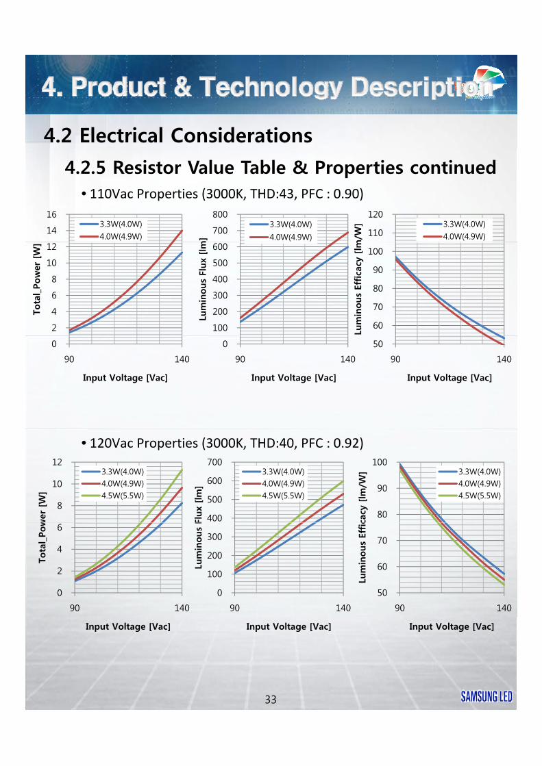
4.2.5 Resistor Value Table & Properties continued• 110Vac Properties (3000K, THD:43, PFC : 0.90)
14
16 3.3W(4.0W)
4.0W(4.9W) 110
120
m/W
] 3.3W(4.0W)
4.0W(4.9W)700
800 m
]
3.3W(4.0W)
4.0W(4.9W)
2
4
6
8
10
12
Tota
l_Pow
er [W
]
60
70
80
90
100
Lum
inous
Effica
cy [
lm
100
200
300
400
500
600
Lum
inous
Flux
[lm
0
90 140
Input Voltage [Vac]
50
90 140
Input Voltage [Vac]
0
90 140
Input Voltage [Vac]
• 120Vac Properties (3000K, THD:40, PFC : 0.92)
8
10
12
wer
[W
]
3.3W(4.0W)4.0W(4.9W)4.5W(5.5W)
80
90
100
cacy
[lm
/W] 3.3W(4.0W)
4.0W(4.9W)4.5W(5.5W)
400
500
600
700
Flux
[lm
]
3.3W(4.0W)4.0W(4.9W)4.5W(5.5W)
0
2
4
6
90 140
Tota
l_Pow
50
60
70
90 140
Lum
inous
Effic
0
100
200
300
90 140
Lum
inous
F
33
Input Voltage [Vac] Input Voltage [Vac]Input Voltage [Vac]

4.2 Electrical Considerations
4.2.5 Resistor Value Table & Properties• 220~240Vac Input Voltage Table
Vin(Vac)
VfBi
Target PKG Power Dissipation*
3.3W *(4.0W**)@ 44 A
4.0W(4.9W)@ 53 A
4.5W(5.5W)@ 58 A(Vac)
Typ.Bin @ 44mA @ 53mA @ 58mA
R [Ω] R [Ω] R [Ω]
220Vac
F1 2200 1700 1500
F3 2100 1650 1460
F5 2000 1600 1430
F1 2620 2100 1900
R R R R
R0 R1Total R = R0+R1
230Vac F3 2560 2050 1850
F5 2500 2000 1800
240Vac
F1 3100 2500 2200
F3 3000 2500 2200
F5 2900 2500 2200 = R0+R1
8.0
10.0
12.0
r [W
]
3.3W(4.0W)
4.0W(4.9W)
4.5W(5.5W)
80
90
100
[lm
/W] 3.3W(4.0W)
4.0W(4.9W)4.5W(5.5W)500
600
700
ux
[lm
] 3.3W(4.0W)4.0W(4.9W)4.5W(5.5W)
• 220Vac Properties (3000K, THD:43, PFC : 0.90)
0.0
2.0
4.0
6.0
200 250
Tota
l_Pow
e
50
60
70
80
200 250
Lum
inous
Effica
cy
0
100
200
300
400
200 250
Lum
inous
Flu
34* LED Power Consumption** Total Power Consumption
Input Voltage [Vac] Input Voltage [Vac]Input Voltage [Vac]

4.2 Electrical Considerations
4.2.5 Resistor Value Table & Properties continued• 230Vac Properties (3000K, THD:40, PFC : 0.91)
8.00
10.00 3.3W(4.0W)
4.0W(4.9W) 90.0
100.0
m/W
] 3.3W(4.0W)
4.0W(4.9W)
4 5W(5 5W)500
600
m]
3.3W(4.0W)4.0W(4.9W)4 5W(5 5W)
2.00
4.00
6.00
8.00
Tota
l_Pow
er [W
] 4.5W(5.5W)
60.0
70.0
80.0
90.0
Lum
inous
Effica
cy [
lm 4.5W(5.5W)
100
200
300
400
Lum
inous
Flux
[lm 4.5W(5.5W)
0.00
200 250
Input Voltage [Vac]
50.0
200 250
Input Voltage [Vac]
0
200 250
Input Voltage [Vac]
• 240Vac Properties (3000K, THD:38, PFC : 0.92)
6.00
8.00
10.00
wer
[W
]
3.3W(4.0W)4.0W(4.9W)4.5W(5.5W)
80.0
90.0
100.0
cacy
[lm
/W] 3.3W(4.0W)
4.0W(4.9W)
4.5W(5.5W)400
500
600
Flux
[lm
]
3.3W(4.0W)4.0W(4.9W)4.5W(5.5W)
0.00
2.00
4.00
210 260
Tota
l_Pow
50.0
60.0
70.0
210 260
Lum
inous
Effic
0
100
200
300
210 260
Lum
inous
F
35
Input Voltage [Vac] Input Voltage [Vac]Input Voltage [Vac]
4.2 Electrical Considerations
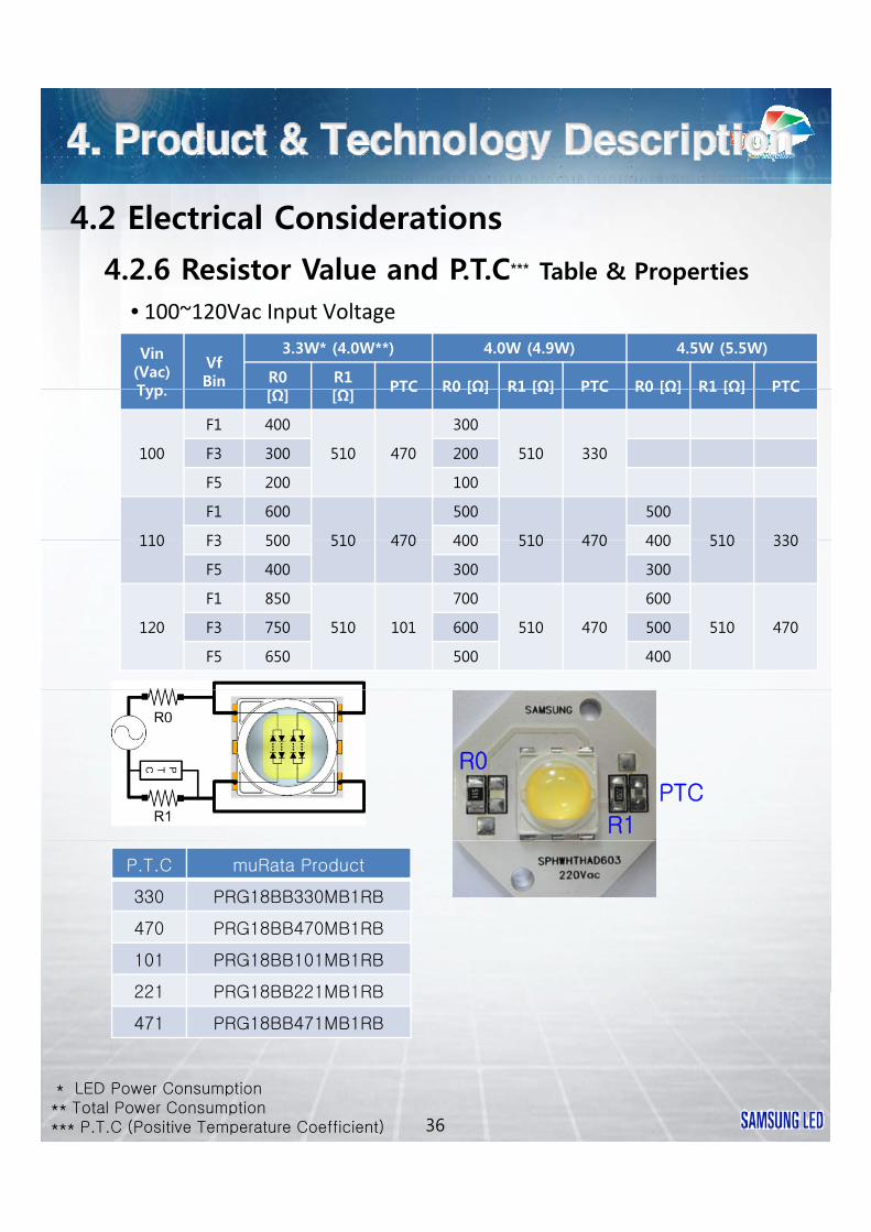
4.2.6 Resistor Value and P.T.C*** Table & Properties
Vin (Vac)Typ
VfBin
3.3W* (4.0W**) 4.0W (4.9W) 4.5W (5.5W)
R0 R1 PTC R0 [Ω] R1 [Ω] PTC R0 [Ω] R1 [Ω] PTC
• 100~120Vac Input Voltage
Typ. [Ω] [Ω]PTC R0 [Ω] R1 [Ω] PTC R0 [Ω] R1 [Ω] PTC
100
F1 400
510 470
300
510 330F3 300 200
F5 200 100
110
F1 600
510 470
500
510 470
500
510 330F3 500 400 400110 510 470 510 470 510 330F3 500 400 400
F5 400 300 300
120
F1 850
510 101
700
510 470
600
510 470F3 750 600 500
F5 650 500 400
R0
R1
PTC
P.T.C muRata Product
330 PRG18BB330MB1RB
470 PRG18BB470MB1RB
101 PRG18BB101MB1RB
221 PRG18BB221MB1RB
36
221 PRG18BB221MB1RB
471 PRG18BB471MB1RB
* LED Power Consumption** Total Power Consumption*** P.T.C (Positive Temperature Coefficient)

4.2 Electrical Considerations
4.2.6 Resistor Value and P.T.C*** Table & Properties
• 100Vac Properties (3000K, THD:48, PFC : 0.87)
10
15
[W
] 4.0W(4.9W)
3.3W(4.0W) 400
500 ux
[lm
]
80
100
120
y [lm
/W]
4.0W(4.9W)
3.3W(4.0W)
0
5
10
80 130
Tota
l pow
er
I t V lt [V ]
0
100
200
300
80 130
Lum
inous
Flu
I t V lt [V ]
4.0W(4.9W)
3.3W(4.0W)
0
20
40
60
80
80 130
Lum
inous
Effica
cy
I t V lt [V ]
• 110Vac Properties (3000K, THD:43, PFC : 0.9)
Input Voltage [Vac] Input Voltage [Vac] Input Voltage [Vac]
6
8
10
12
wer
[W
] 3.3W(4.0W)
4.0W(4.9W)
4.5W(5.5W) 300
400
500
Flux
[lm
]
100
150
cacy
[lm
/W]
0
2
4
6
80 130
Tota
l pow
Input Voltage [Vac]
0
100
200
80 130
Lum
inous
Input Voltage [Vac]
3.3W(4.0W)
4.0W(4.9W)
4.5W(5.5W)
0
50
80 130
Lum
inous
Effic
Input Voltage [Vac]
3.3W(4.0W)4.0W(4.9W)4.5W(5.5W)
• 120Vac Properties (3000K, THD:39, PFC : 0.91)
4
6
8
10
l Pow
er [W
] 3.3W(4.0W)
4.5W(5.5W)
200
300
400
500
ous
Flux
[lm
]
40
60
80
100
120
Effica
cy [
lm/W
]
3.3W(4.0W)
37
0
2
80 130
Tota
Input Voltage [Vac]
0
100
80 130
Lum
in
Input Voltage [Vac]
3.3W(4.0W)
4.5W(5.5W)
0
20
40
80 130
Lum
inous
Input Voltage [Vac]
( )
4.5W(5.5W)

4.2 Electrical Considerations
• 220~240Vac Input Voltage
Vin(Vac)Typ
VfBin
3.3W* (4.0W**) 4.0W (4.9W) 4.5W (5.5W)
R0 R1 PTC R0 [Ω] R1 [Ω] PTC R0 [Ω] R1 [Ω] PTC
4.2.6 Resistor Value and P.T.C*** Table & Properties
Typ. [Ω] [Ω]PTC R0 [Ω] R1 [Ω] PTC R0 [Ω] R1 [Ω] PTC
220
F1 2200
2000 471
1750
2000 221
1700
2000 101F3 2100 1650 1600
F5 2000 1550 1500
230
F1 2800
2000 471
2300
2000 221
2100
2000 101F3 2700 2200 2000230 2000 471 2000 221 2000 101F3 2700 2200 2000
F5 2600 2100 1900
R0
PTC
R1
PTC
P.T.C muRata Product
330 PRG18BB330MB1RB
470 PRG18BB470MB1RB
101 PRG18BB101MB1RB
221 PRG18BB221MB1RB
38
* LED Power Consumption** Total Power Consumption*** P.T.C (Positive Temperature Coefficient)
221 PRG18BB221MB1RB
471 PRG18BB471MB1RB
4.2 Electrical Considerations
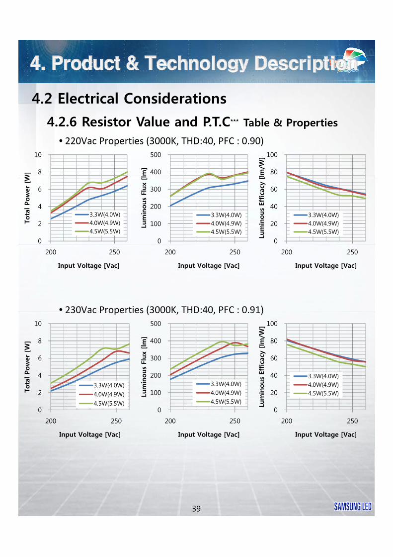
• 220Vac Properties (3000K, THD:40, PFC : 0.90)
4.2.6 Resistor Value and P.T.C*** Table & Properties
8
10
W] 400
500
m]
80
100
lm/W
]
0
2
4
6
Tota
l Pow
er [W
3.3W(4.0W)4.0W(4.9W)4.5W(5.5W)
0
100
200
300
Lum
inous
Flux
[l
3.3W(4.0W)4.0W(4.9W)4.5W(5.5W)
0
20
40
60
Lum
inous
Effica
cy [
l
3.3W(4.0W)4.0W(4.9W)4.5W(5.5W)
• 230Vac Properties (3000K, THD:40, PFC : 0.91)
200 250
Input Voltage [Vac]
200 250
Input Voltage [Vac]
200 250
Input Voltage [Vac]
230Vac Properties (3000K, THD:40, PFC : 0.91)
4
6
8
10
al P
ow
er [W
]
200
300
400
500
nous
Flux
[lm
]
40
60
80
100
s Ef
fica
cy [
lm/W
]
3.3W(4.0W)
0
2
200 250
Tota
Input Voltage [Vac]
3.3W(4.0W)
4.0W(4.9W)
4.5W(5.5W)0
100
200 250
Lum
in
Input Voltage [Vac]
3.3W(4.0W)
4.0W(4.9W)
4.5W(5.5W)0
20
200 250
Lum
inou
Input Voltage [Vac]
4.0W(4.9W)4.5W(5.5W)
39
4.2 Electrical Considerations
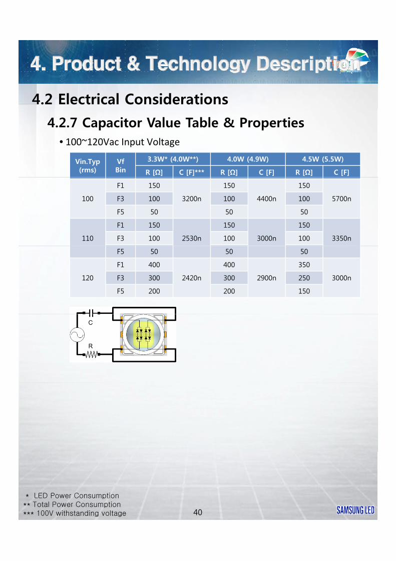
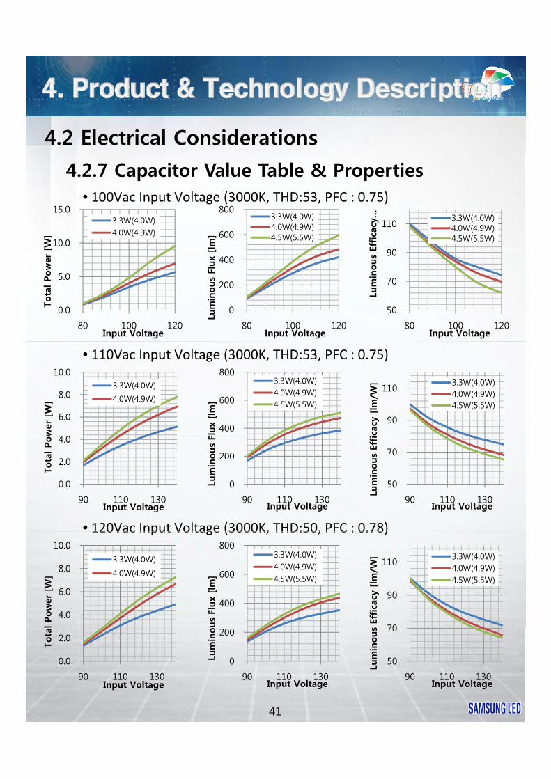
4.2.7 Capacitor Value Table & Properties• 100~120Vac Input Voltage
Vin.Typ(rms)
VfBin
3.3W* (4.0W**) 4.0W (4.9W) 4.5W (5.5W)
R [Ω] C [F]*** R [Ω] C [F] R [Ω] C [F]
100
F1 150
3200n
150
4400n
150
5700nF3 100 100 100
F5 50 50 50
110
F1 150
2530n
150
3000n
150
3350nF3 100 100 100
F5 50 50 50
120
F1 400
2420n
400
2900n
350
3000nF3 300 300 250
F5 200 200 150
40
* LED Power Consumption** Total Power Consumption*** 100V withstanding voltage
4.2 Electrical Considerations
4.2.7 Capacitor Value Table & Properties• 100Vac Input Voltage (3000K, THD:53, PFC : 0.75)
10.0
15.0
W]
3.3W(4.0W)4.0W(4.9W) 600
800 m
]3.3W(4.0W)4.0W(4.9W)4.5W(5.5W)
110
ffic
acy … 3.3W(4.0W)
4.0W(4.9W)4.5W(5.5W)
0.0
5.0
0.0
80 100 120
Tota
l Pow
er [W
Input Voltage
0
200
400
80 100 120
Lum
inous
Flux
[l
Input Voltage
50
70
90
80 100 120
Lum
inous
Ef
Input Voltage
• 110Vac Input Voltage (3000K, THD:53, PFC : 0.75)
4 0
6.0
8.0
10.0
wer
[W
]
3.3W(4.0W)
4.0W(4.9W)
400
600
800
Flux
[lm
]
3.3W(4.0W)4.0W(4.9W)4.5W(5.5W)
90
110
icac
y [lm
/W] 3.3W(4.0W)
4.0W(4.9W)4.5W(5.5W)
• 120Vac Input Voltage (3000K, THD:50, PFC : 0.78)
0.0
2.0
4.0
90 110 130
Tota
l Po
Input Voltage
0
200
90 110 130
Lum
inous
F
Input Voltage
50
70
90 110 130
Lum
inous
Effi
Input Voltage
120Vac Input Voltage (3000K, THD:50, PFC : 0.78)
4.0
6.0
8.0
10.0
l Pow
er [W
]
3.3W(4.0W)
4.0W(4.9W)
400
600
800
us
Flux
[lm
]
3.3W(4.0W)4.0W(4.9W)4.5W(5.5W)
70
90
110
Eff
icac
y [lm
/W] 3.3W(4.0W)
4.0W(4.9W)4.5W(5.5W)
41
0.0
2.0
90 110 130
Tota
l
Input Voltage
0
200
90 110 130
Lum
ino
Input Voltage
50
70
90 110 130
Lum
inous
Input Voltage
4.2 Electrical Considerations
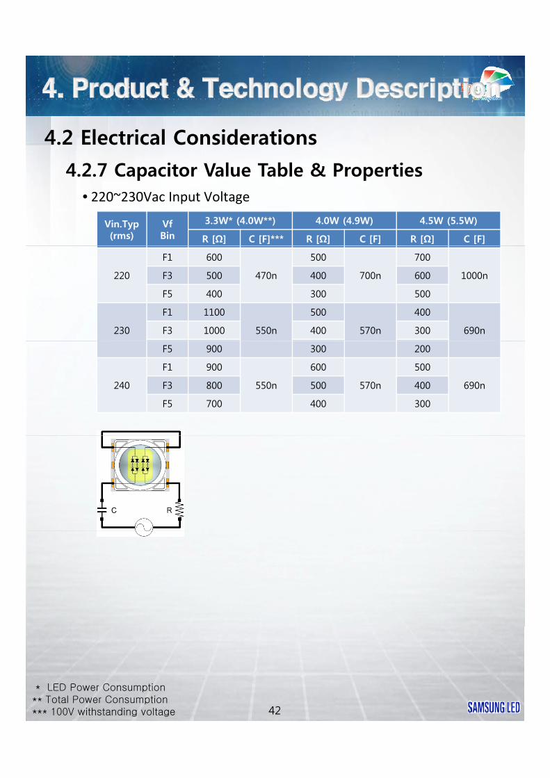
4.2.7 Capacitor Value Table & Properties• 220~230Vac Input Voltage
Vin.Typ(rms)
VfBin
3.3W* (4.0W**) 4.0W (4.9W) 4.5W (5.5W)
R [Ω] C [F]*** R [Ω] C [F] R [Ω] C [F]
220
F1 600
470n
500
700n
700
1000nF3 500 400 600
F5 400 300 500
230
F1 1100
550n
500
570n
400
690nF3 1000 400 300
F5 900 300 200
240
F1 900
550n
600
570n
500
690nF3 800 500 400
F5 700 400 300
42
* LED Power Consumption** Total Power Consumption*** 100V withstanding voltage

4.2 Electrical Considerations
4.2.7 Capacitor Value Table & Properties• 220Vac Input Voltage (3000K, THD:50, PFC : 0.73)
6.0
8.0
W]
400
500 m
]
90
100
lm/W
]
0.0
2.0
4.0
200 220 240
Tota
l Pow
er [W
3.3W(4.0W)
4.0W(4.9W)0
100
200
300
200 220 240
Lum
inous
Flux
[lm
3.3W(4.0W)4.0W(4.9W)4.5W(5.5W)
50
60
70
80
200 220 240
Lum
inous
Effica
cy [
3.3W(4.0W)4.0W(4.9W)4.5W(5.5W)
• 230Vac Input Voltage (3000K, THD:50, PFC : 0.73)
200 220 240Input Voltage
200 220 240Input Voltage
200 220 240Input Voltage
4 0
6.0
8.0
er [W
]
300
400
500
x [lm
]
80
90
100 ac
y [lm
/W]
0.0
2.0
4.0
200 220 240
Tota
l Pow
e
Input Voltage
3.3W(4.0W)
4.0W(4.9W)0
100
200
200 220 240
Lum
inous
Flux
Input Voltage
3.3W(4.0W)4.0W(4.9W)4.5W(5.5W)
50
60
70
200 220 240
Lum
inous
Effica
Input Voltage
3.3W(4.0W)4.0W(4.9W)4.5W(5.5W)
• 240Vac Input Voltage (3000K, THD:50, PFC : 0.73)
3.0
4.0
5.0
6.0
ow
er [W
]
200
300
400
500
Flux
[lm
]
70
80
90
100
ffic
acy
[lm
/W]
43
0.0
1.0
2.0
210 230 250
Tota
l P
Input Voltage
3.3W(4.0W)
4.0W(4.9W)0
100
200
210 230 250
Lum
inous
Input Voltage
3.3W(4.0W)
4.0W(4.9W)
50
60
70
210 230 250
Lum
inous
Ef
Input Voltage
3.3W(4.0W)
4.0W(4.9W)
4.2 Electrical Considerations
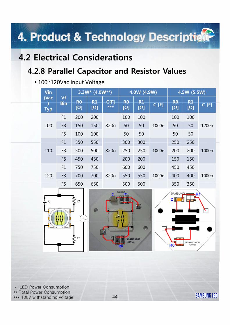
4.2.8 Parallel Capacitor and Resistor Values
Vin(Vac
)VfBin
3.3W* (4.0W**) 4.0W (4.9W) 4.5W (5.5W)
R0 R1 C[F] R0 R1 R0 R1
• 100~120Vac Input Voltage
)Typ
Bin R0 [Ω]
R1 [Ω]
C[F]***
R0 [Ω]
R1 [Ω]
C [F]R0 [Ω]
R1 [Ω]
C [F]
100
F1 200 200
820n
100 100
1000n
100 100
1200nF3 150 150 50 50 50 50
F5 100 100 50 50 50 50
F1 550 550 300 300 250 250
110
F1 550 550
820n
300 300
1000n
250 250
1000nF3 500 500 250 250 200 200
F5 450 450 200 200 150 150
120
F1 750 750
820n
600 600
1000n
450 450
1000nF3 700 700 550 550 400 400
F5 650 650 500 500 350 350
44
* LED Power Consumption** Total Power Consumption*** 100V withstanding voltage
4.2 Electrical Considerations
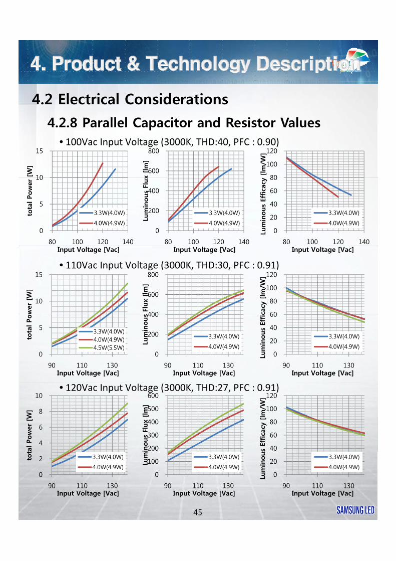
4.2.8 Parallel Capacitor and Resistor Values• 100Vac Input Voltage (3000K, THD:40, PFC : 0.90)
10
15
[W]
600
800 x
[lm
]
80
100
120
[lm
/W]
0
5
10
80 100 120 140
tota
l Pow
er
3.3W(4.0W)
4.0W(4.9W)0
200
400
80 100 120 140
Lum
inous
Flux
3.3W(4.0W)
4.0W(4.9W)0
20
40
60
80
80 100 120 140
Lum
inous
Effica
cy
3.3W(4.0W)
4.0W(4.9W)
• 110Vac Input Voltage (3000K, THD:30, PFC : 0.91)
Input Voltage [Vac] Input Voltage [Vac] Input Voltage [Vac]
10
15
wer
[W
]
400
600
800
s Fl
ux
[lm
]
60
80
100
120
cacy
[lm
/W]
0
5
90 110 130
tota
l Pow
Input Voltage [Vac]
3.3W(4.0W)4.0W(4.9W)4.5W(5.5W)
0
200
400
90 110 130
Lum
inous
Input Voltage [Vac]
3.3W(4.0W)
4.0W(4.9W)0
20
40
60
90 110 130
Lum
inous
Effic
Input Voltage [Vac]
3.3W(4.0W)
4.0W(4.9W)
• 120Vac Input Voltage (3000K, THD:27, PFC : 0.91)
4
6
8
10
tal Pow
er [W
]
200
300
400
500
600
inous
Flux
[lm
]
40
60
80
100
120
s Ef
fica
cy [
lm/W
]
45
0
2
90 110 130
tot
Input Voltage [Vac]
3.3W(4.0W)
4.0W(4.9W)0
100
90 110 130
Lum
i
Input Voltage [Vac]
3.3W(4.0W)
4.0W(4.9W)0
20
90 110 130
Lum
inou
Input Voltage [Vac]
3.3W(4.0W)
4.0W(4.9W)

4.2 Electrical Considerations
4.2.9 Capacitor Value Table & Properties• 220~240Vac Input Voltage
Vin(Vac Vf
i
3.3W* (4.0W**) 4.0W (4.9W) 4.5W (5.5W)
R0 R1 R0 R1 R0 R1)Typ
Bin R0 [Ω]
R1 [Ω]
C [F]R0 [Ω]
R1 [Ω]
C [F]R0 [Ω]
R1 [Ω]
C [F]
200
F1 900
800 200n
650
550 200n
550
450 200nF3 800 550 450
F5 700 450 350
F1 1400 1100 900
220
F1 1400
1300 200n
1100
1000 200n
900
1000 200nF3 1300 1000 800
F5 1200 900 700
230
F1 1850
1750 200n
1350
1250 200n
1200
1100 200nF3 1750 1250 1100
F5 1650 1150 1000
240
F1 2250
2150 200n
1650
1550 200n
1500
1400 200nF3 2150 1550 1400
F5 2050 1450 1300
46
* LED Power Consumption** Total Power Consumption*** 250V withstanding voltage

4.2 Electrical Considerations
4.2.9 Capacitor Value Table & Properties• 220Vac Input Voltage (3000K, THD:25, PFC : 0.95)
8
10
[W] 500
600 [lm
]
80
100
[lm
/W]
0
2
4
6
200 220 240
tota
l Pow
er [
3.3W(4.0W)4.0W(4.9W)4.5W(5.5W)
0
100
200
300
400
200 220 240
Lum
inous
Flux
3.3W(4.0W)4.0W(4.9W)4.5W(5.5W)
0
20
40
60
200 220 240
Lum
inous
Effica
cy [
3.3W(4.0W)4.0W(4.9W)4.5W(5.5W)
• 230Vac Input Voltage (3000K, THD:25, PFC : 0.95)
200 220 240Input Voltage [Vac]
200 220 240Input Voltage [Vac]
200 220 240Input Voltage [Vac]
6
8
wer
[W
]
400
500
600
Flux
[lm
]
60
80
100
acy
[lm
/W]
0
2
4
200 220 240
tota
l Pow
Input Voltage [Vac]
3.3W(4.0W)4.0W(4.9W)4.5W(5.5W)
0
100
200
300
200 220 240
Lum
inous
F
Input Voltage [Vac]
3.3W(4.0W)4.0W(4.9W)4.5W(5.5W)
0
20
40
200 220 240
Lum
inous
Effica
Input Voltage [Vac]
3.3W(4.0W)4.0W(4.9W)4.5W(5.5W)
• 240Vac Input Voltage (3000K, THD:25, PFC : 0.95)
4
6
8
Pow
er [W
]
200
300
400
500
ous
Flux
[lm
]
40
60
80
100
Effica
cy [
lm/W
]
47
0
2
210 230 250
tota
l
Input Voltage [Vac]
3.3W(4.0W)4.0W(4.9W)4.5W(5.5W)
0
100
200
210 230 250
Lum
ino
Input Voltage [Vac]
3.3W(4.0W)4.0W(4.9W)4.5W(5.5W)
0
20
40
210 230 250
Lum
inous
E
Input Voltage [Vac]
3.3W(4.0W)4.0W(4.9W)4.5W(5.5W)
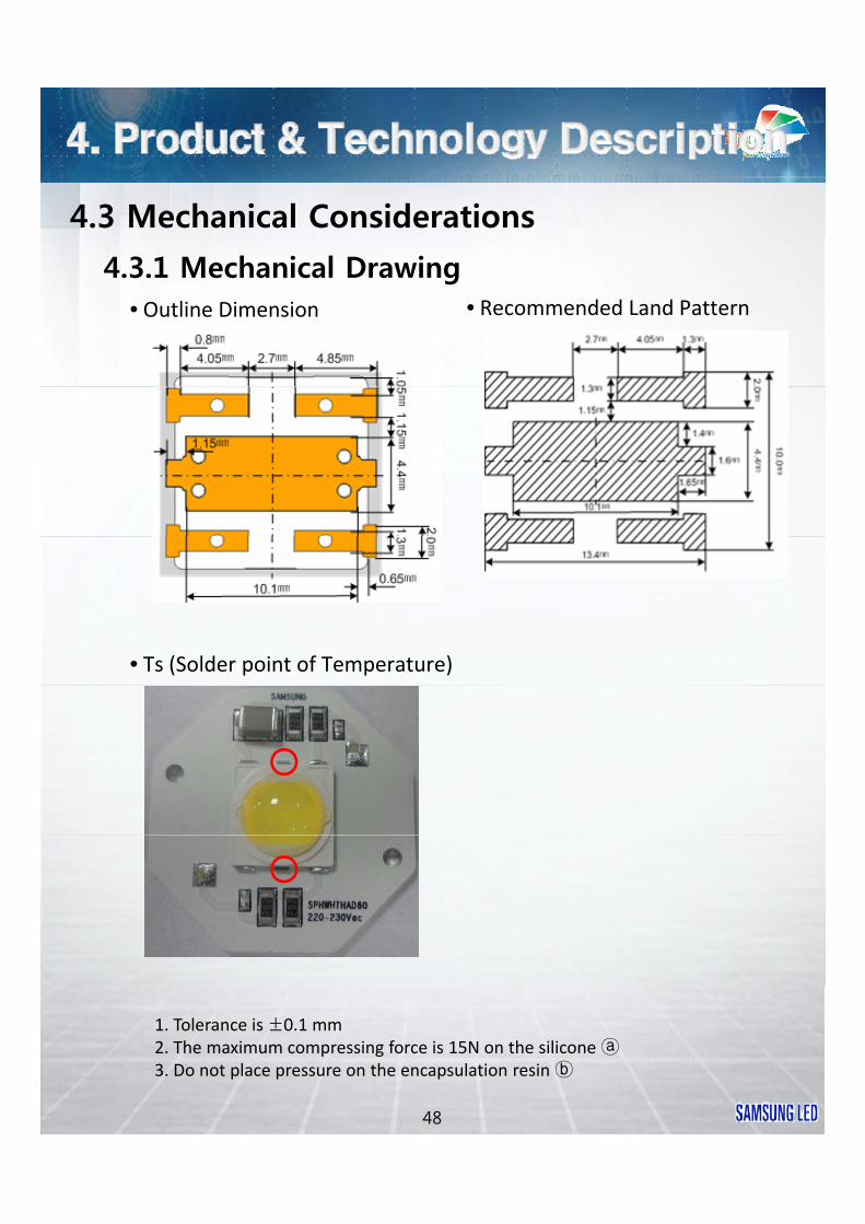
4.3 Mechanical Considerations
4.3.1 Mechanical Drawing• Outline Dimension • Recommended Land Pattern
• Ts (Solder point of Temperature)
48
1. Tolerance is ±0.1 mm2. The maximum compressing force is 15N on the silicone 3. Do not place pressure on the encapsulation resin
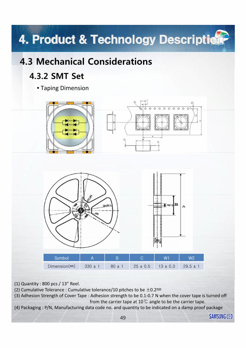
4.3 Mechanical Considerations
4.3.2 SMT Set• Taping Dimension
Symbol A B C W1 W2
Dimension() 330 ± 1 80 ± 1 25 ± 0.5 13 ± 0.3 29.5 ± 1
49
(1) Quantity : 800 pcs / 13” Reel.(2) Cumulative Tolerance : Cumulative tolerance/10 pitches to be ±0.2(3) Adhesion Strength of Cover Tape : Adhesion strength to be 0.1‐0.7 N when the cover tape is turned off
from the carrier tape at 10 angle to be the carrier tape.(4) Packaging : P/N, Manufacturing data code no. and quantity to be indicated on a damp proof package

4.3 Mechanical Considerations
Pick‐up and Place for HA04J
‐ SMT Equipment process and its conditions
4.3.2 SMT Set
Process DefinitionTime (msec)
Pressure(mmhg)
Pick‐up Pick‐up PKG from taping reel 200
223Place Place PKG to PCB 120
Dump Dump the faulty PKG 50
‐ Pick up tool (collet)
※ Samsung SM421 Chip mounter
Unit : mm
50
※ These reference value could be changed by circumstance and condition of Customer.

4.3 Mechanical Considerations
Reflow conditions and work guide
4.3.3 Reflow Profile
Below reflow profile is recommended for reflow soldering.
It may not apply for all PCB kinds and various soldering equipment.
It is recommended that users follow the recommended reflow profile
of a solder manufacturer
For Manual Soldering
Not more than 5 seconds @MAX300 , under soldering iron.
51
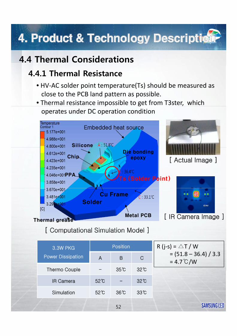
4.4 Thermal Considerations
4.4.1 Thermal Resistance• HV‐AC solder point temperature(Ts) should be measured as close to the PCB land pattern as possible.
• Thermal resistance impossible to get from T3ster, whichp goperates under DC operation condition
Silicone
Embedded heat source
PPA
ChipDie bonding
epoxy
Ts (Solder Point)
[ Actual Image ]
Cu Frame
Metal PCBThermal grease
Solder
[ Computational Simulation Model ]
[ IR Camera Image ]
[ Computational Simulation Model ]
3.3W PKG
Power Dissipation
Position
A B C
Thermo Couple - 35 32
R (j‐s) = T / W= (51.8 – 36.4) / 3.3= 4.7/W
52
Thermo Couple 35 32
IR Camera 52 - 32
Simulation 52 36 33

5.1 Dimming
5.1.1 Recommended Dimmer
• Low voltage dimmer is well matching with HV‐AC
www.lutron.com
• Lutron DVELV‐300P
50100150200250300
lx
0
0 50 100
Dimming level…
wwwairtecsys comwww.airtecsys.com
Slide Type Button Type Rotary Type
Specifications• Model ATS‐ALD100W‐BD• Rated Voltage 110 ~230Vac ±10%• Frequency 50 ~ 60Hz
53
• Rated Power 100W(220Vac), 50W(110Vac)• Dimming Range 0 ~ 100%• Available Lamp AC‐LED • Option Remote Control
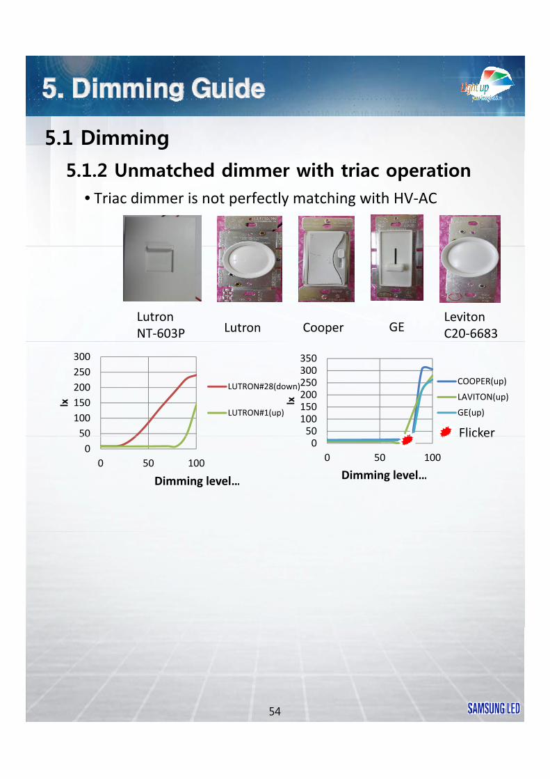
5.1 Dimming
5.1.2 Unmatched dimmer with triac operation• Triac dimmer is not perfectly matching with HV‐AC
LutronNT‐603P GE
Leviton C20‐6683Lutron Cooper
50100150200250300350
lx
COOPER(up)
LAVITON(up)
GE(up)
50
100
150
200
250
300
lx
LUTRON#28(down)
LUTRON#1(up)
Flicker0
0 50 100
Dimming level…
0
50
0 50 100
Dimming level…
Flicker
54

6.1 UL, cUL (Approved Jun ‘11)
55* UL : Underwriters Laboratories* cUL : Canada UL

6.2 CE, VDE (Approved April ‘11)
• Safety(LVD) ‐ DIN EN 62031(VDE 0715 Teil5) LED modules for
general lighting — Safety specificationsgeneral lighting — Safety specifications‐ EN 62471 Photo Biological safety of lamps and
lamp systems• EMC‐ DIN EN 55015, EN 55015‐ DIN EN 61547, EN61547‐ DIN EN 61000‐3‐2 EN 61000‐3‐2DIN EN 61000 3 2, EN 61000 3 2‐ DIN EN 61000‐3‐3, EN 61000‐3‐3
EUT upside
Radiated Emission Disturbance Magnetic Field Emission
56
Field strength Setup Measurement Setup
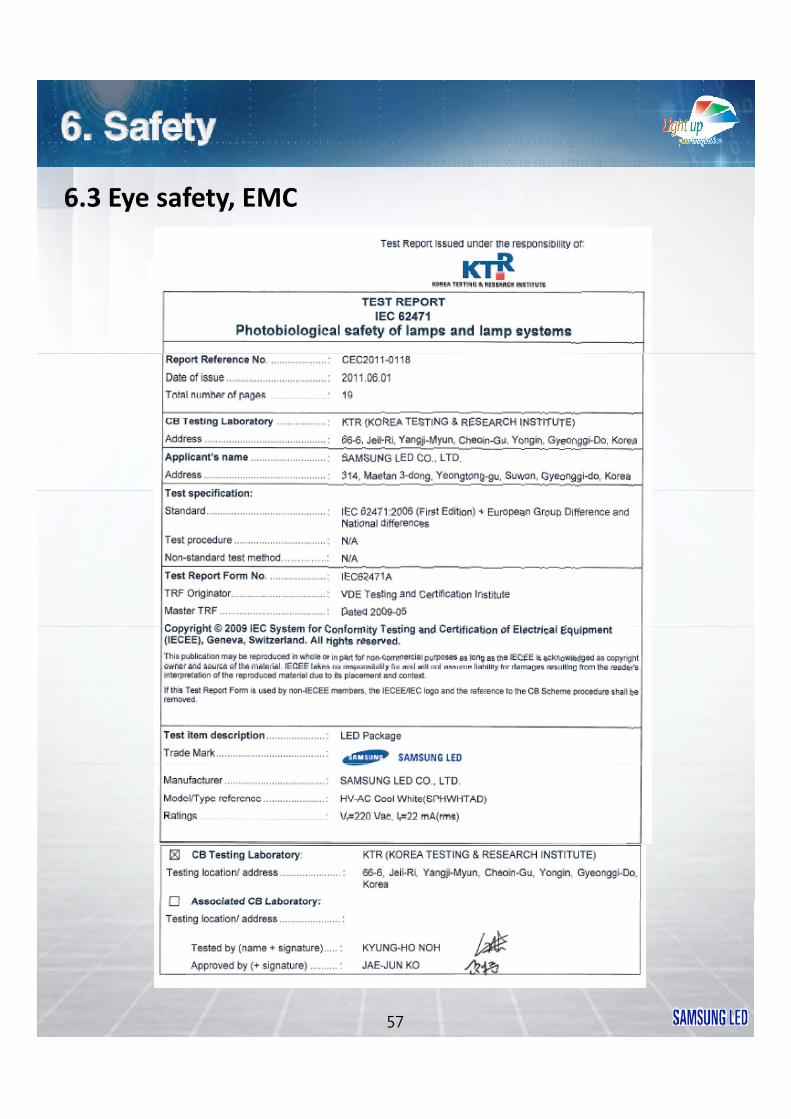
6.3 Eye safety, EMC
57

6.4 RoHS, Hazard Substance Analysis
58

6.4 RoHS, Hazard Substance Analysis
59
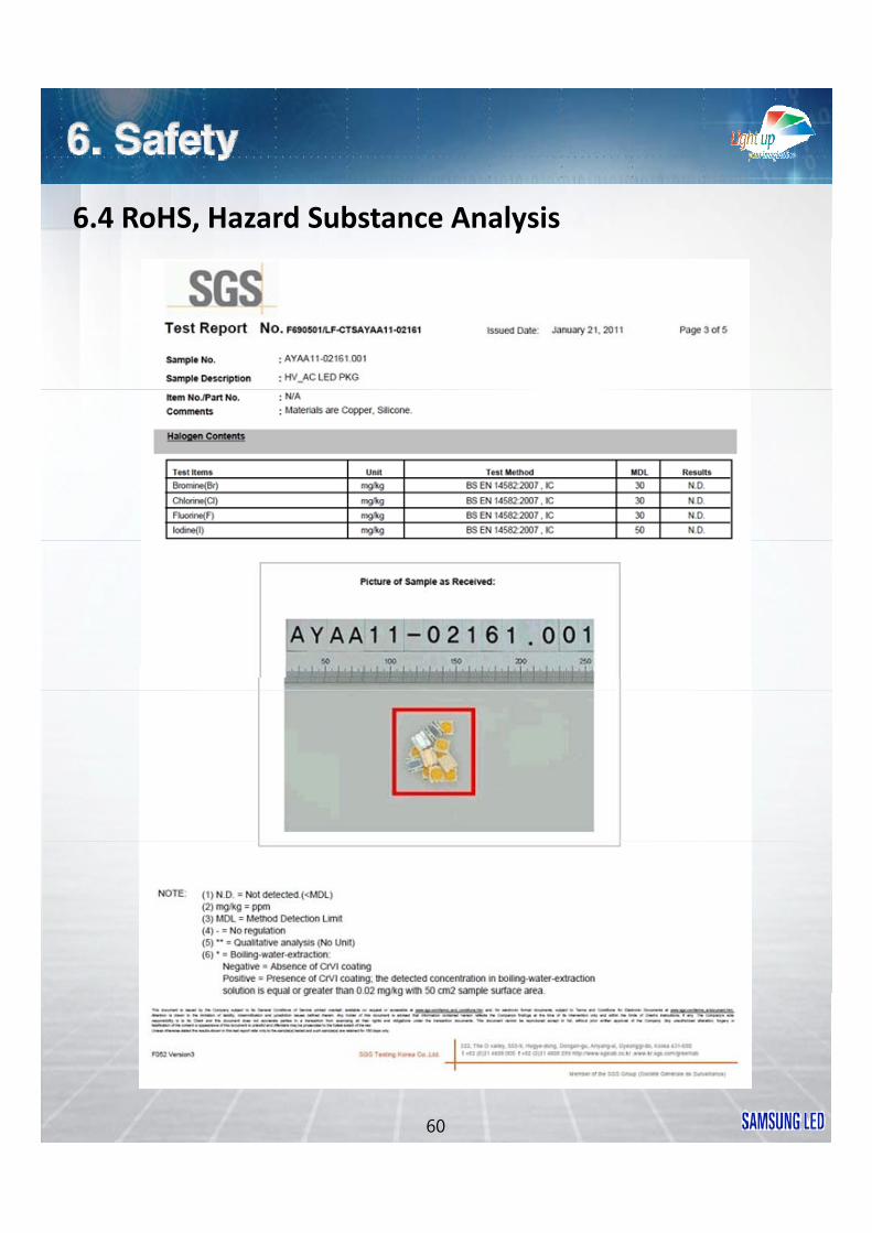
6.4 RoHS, Hazard Substance Analysis
60
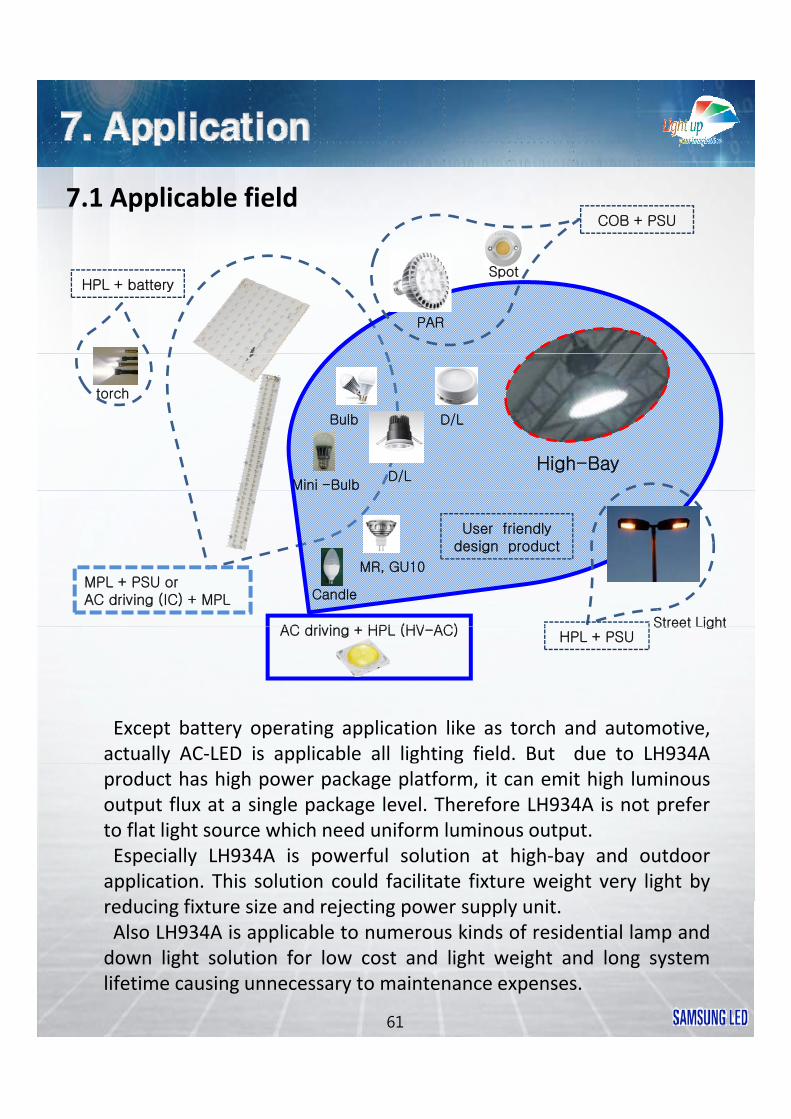
7.1 Applicable fieldCOB + PSU
Spot
PAR
COB + PSU
HPL + battery
torch
D/L
D/L
Bulb
Mini -Bulb
High-Bay
AC d i i + HPL (HV AC)
MPL + PSU orAC driving (IC) + MPL Candle
MR, GU10
User friendly design product
Street LightAC driving + HPL (HV-AC) HPL + PSU
Street ight
Except battery operating application like as torch and automotive,actually AC‐LED is applicable all lighting field. But due to LH934Aproduct has high power package platform, it can emit high luminousoutput flux at a single package level. Therefore LH934A is not preferto flat light source which need uniform luminous output.Especially LH934A is powerful solution at high‐bay and outdoorapplication. This solution could facilitate fixture weight very light byd i fi t i d j ti l it
61
reducing fixture size and rejecting power supply unit.Also LH934A is applicable to numerous kinds of residential lamp anddown light solution for low cost and light weight and long systemlifetime causing unnecessary to maintenance expenses.
7.2 Design guide
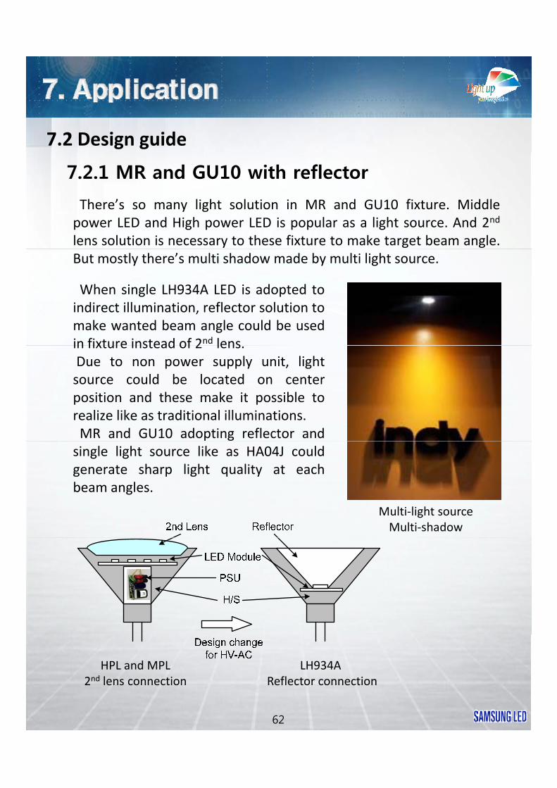
7.2.1 MR and GU10 with reflector
There’s so many light solution in MR and GU10 fixture. Middlepower LED and High power LED is popular as a light source. And 2nd
lens solution is necessary to these fixture to make target beam angle.But mostly there’s multi shadow made by multi light source.
When single LH934A LED is adopted toindirect illumination, reflector solution tomake wanted beam angle could be usedin fixture instead of 2nd lensin fixture instead of 2 lens.Due to non power supply unit, lightsource could be located on centerposition and these make it possible torealize like as traditional illuminations.MR and GU10 adopting reflector and
Multi‐light sourceMulti‐shadow
single light source like as HA04J couldgenerate sharp light quality at eachbeam angles.
62
HPL and MPL2nd lens connection
LH934A Reflector connection
7.2 Design guide
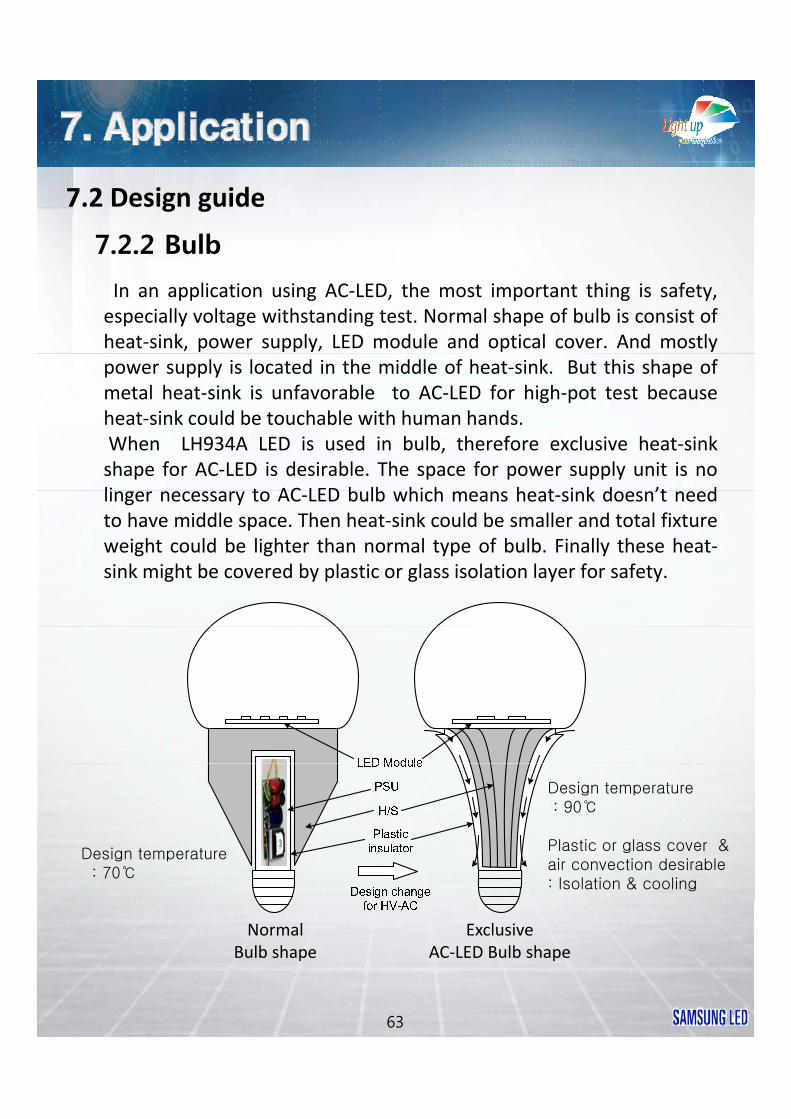
7.2.2 Bulb
In an application using AC‐LED, the most important thing is safety,especially voltage withstanding test. Normal shape of bulb is consist ofheat‐sink, power supply, LED module and optical cover. And mostlypower supply is located in the middle of heat‐sink. But this shape ofmetal heat‐sink is unfavorable to AC‐LED for high‐pot test becauseheat‐sink could be touchable with human hands.When LH934A LED is used in bulb, therefore exclusive heat‐sinkshape for AC‐LED is desirable. The space for power supply unit is noli t AC LED b lb hi h h t i k d ’t dlinger necessary to AC‐LED bulb which means heat‐sink doesn’t needto have middle space. Then heat‐sink could be smaller and total fixtureweight could be lighter than normal type of bulb. Finally these heat‐sink might be covered by plastic or glass isolation layer for safety.
Design temperature: 70
Design temperature: 90
Plastic or glass cover & air convection desirable: Isolation & cooling
63
NormalBulb shape
ExclusiveAC‐LED Bulb shape
7.3 2nd Lens Solution
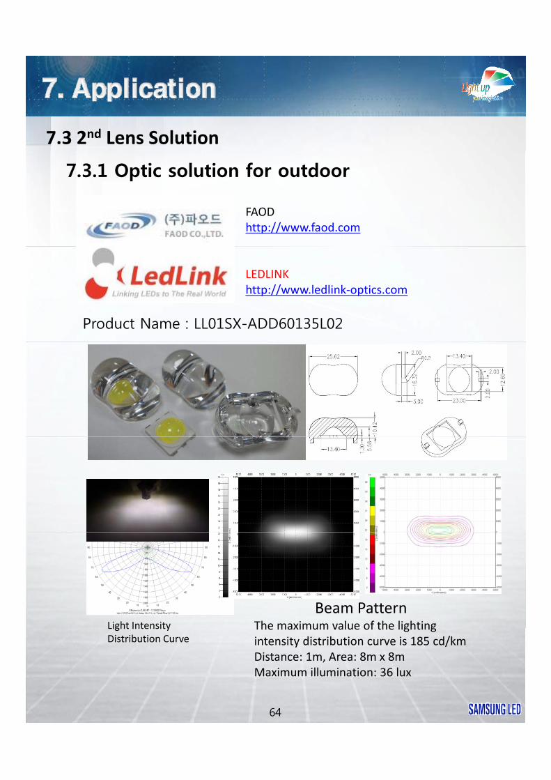
7.3.1 Optic solution for outdoor
FAOD http://www.faod.com
LEDLINKhttp://www.ledlink‐optics.com
Product Name : LL01SX-ADD60135L02
Light Intensity
Beam PatternThe maximum value of the lighting
64
Light IntensityDistribution Curve
The maximum value of the lighting intensity distribution curve is 185 cd/kmDistance: 1m, Area: 8m x 8mMaximum illumination: 36 lux
7.3 2nd Lens Solution
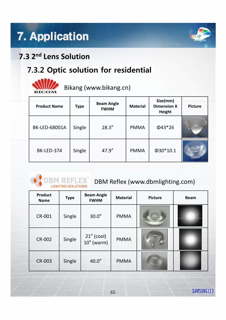
7.3.2 Optic solution for residential
Bikang (www.bikang.cn)
Size(mm)Product Name Type
Beam AngleFWHM
MaterialSize(mm)
Dimension X Height
Picture
BK‐LED‐68001A Single 28.3° PMMA Φ43*26
BK‐LED‐374 Single 47.9° PMMA Φ30*10.1
fl ( db li h i )DBM Reflex (www.dbmlighting.com)
ProductName
TypeBeam Angle
FWHMMaterial Picture Beam
CR‐001 Single 30.0° PMMAg
CR‐002 Single21° (cool)10° (warm)
PMMA
65
CR‐003 Single 40.0° PMMA

Date Revision HistoryWriter
D A dDrawn Approved
2012.03.23 New Version Y. J. Lee D. M. Jeon
2012.04.13 -. Driving component table changed at 120Vac Y. J. Lee D. M. Jeon
-. Additional dimming solution inserted (p.54)- Additional VDE certification inserted (p 57)
2012.08.10
. Additional VDE certification inserted (p.57)-. Application information added (p.62~66)
. Applicable field
. Design guide
. 2nd lens solution
Y. J. Lee D. M. Jeon
2012.10.17 -. SMT Nozzle information up-date (p.50) Y. J. Lee D. M. Jeon
2012 12 27 Naming changed (HA04J LH934A) Y J Lee D M Jeon2012.12.27 -. Naming changed (HA04J LH934A) Y. J. Lee D. M. Jeon
66