
Application Note MP1800A - dl.cdn-anritsu.com · Application Note Optical Module Testing Anritsu...
15
Application Note MP1800A Signal Quality Analyzer Optical Module Testing
Transcript of Application Note MP1800A - dl.cdn-anritsu.com · Application Note Optical Module Testing Anritsu...

Application Note
MP1800ASignal Quality Analyzer Optical Module Testing

1
Slide 1
2006 10
MP1800 Series Signal Quality Analyzer MP1800 Series Signal Quality Analyzer Application NoteApplication Note
Optical Module TestingOptical Module Testing
Anritsu CorporationMeasurement Business Group
IP Network Measurement Division
MP1800 Series Signal Quality Analyzer Application Note: MBP-106301-00
Slide 2
2006 10
ContentsContents
1. Network Overview2. Various High-Speed Interfaces3. Network Equipment Composition4. Optical Transceivers (MSA Modules)5. XFP Block Diagram6. Optical Transceiver Manufacturing Process 7. Key Measurement Parameters8. Measurement Procedures9. Appendix
2
Slide 3
2006 10
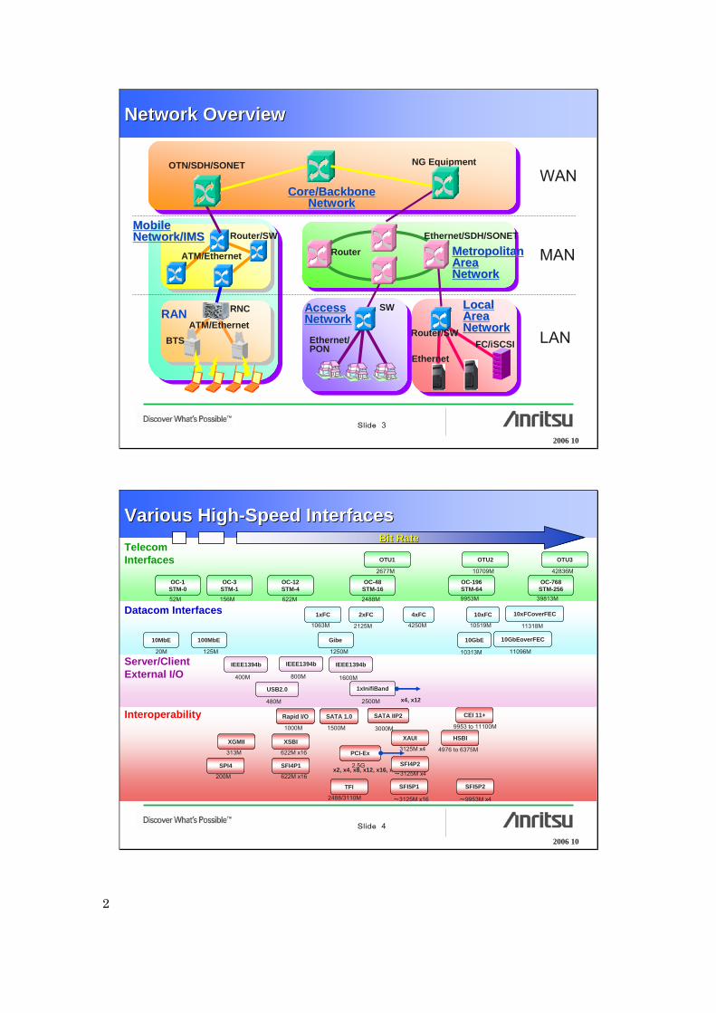
Network OverviewNetwork Overview
Core/BackboneCore/BackboneNetworkNetwork
MetropolitanMetropolitanAreaAreaNetworkNetwork
AccessAccessNetworkNetwork
MobileMobileNetwork/IMSNetwork/IMS
RAN
OTN/SDH/SONET
Ethernet/SDH/SONET
Ethernet/PON
ATM/Ethernet
ATM/Ethernet
BTS
RNC SW
Router
Router/SW
NG Equipment
LocalLocalAreaAreaNetworkNetwork
EthernetFC/iSCSI
Router/SW LAN
MAN
WAN
Slide 4
2006 10
Various HighVarious High--Speed InterfacesSpeed Interfaces
OC-1STM-0
OC-3STM-1
OC-12STM-4
OC-48STM-16
OC-196STM-64
OC-768STM-256
OTU1 OTU2 OTU3
52M 156M 622M 2488M 9953M 39813M
2677M 10709M 42836M
Telecom Interfaces
IEEE1394b
1xInifiBand
IEEE1394b IEEE1394b
400M 800M 1600M
2500M
USB2.0
480M
Server/ClientExternal I/O
x4, x12
1xFC
Gibe
2xFC 4xFC
1250M
1063M 2125M 4250M
Datacom Interfaces 10xFC
10GbE
10519M
10313M
10GbEoverFEC
11096M
10xFCoverFEC
11318M
SATA 1.0
1500M
SATA IIP2
3000M
Interoperability
2500MPCI-Ex
x2, x4, x8, x12, x16, x32
XAUI
3125M x4
HSBI
4976 to 6375M
SFI4P2~3125M x4
SPI4
200M
SFI4P1
622M x16
Rapid I/O
1000M
XSBI
622M x16
XGMII
313M
CEI 11+
9953 to 11100M
SFI5P1
~3125M x16
TFI
2488/3110M
Bit RateBit Rate
10MbE
20M
100MbE
125M
2.5G
SFI5P2
~9953M x4

3
Slide 5
2006 10
Network Equipment CompositionNetwork Equipment Composition
Interface Card
TOSA/ROSA
Transmission Equipment /Switch/Router
SFP/SFF/GBICXFP/XPAK/X2/XENPAKOptical Transceiver
TOSA/ROSA/BOSASubassembly
CAN type LD/PD, PHY ICOptical Parts
LD/PD ChipDevice
Optical Transceiver
Slide 6
2006 10
Optical Transceivers (MSA Modules)Optical Transceivers (MSA Modules)
10G/40GSmall, SFI-4P2SFI-4P2/PCI CardSmall, XAUI supportSmallSmallFeatures
SDH/SONETSDH/SONET10GbE/FEC
10GbE10GbESDH/SONET10GbE/10GFC
ATM/FDDI/FC/GibeSDH/SONET
Application
x16 (SFI-4P1)x16 (SFI-5P1)
x4 (XAUI/SFI-4P2)x4 (XAUI/SFI-4P2)x4 (XAUI)SerialSerial Electrical I/F
10G/40G9.95 to 11.2G10.3G10.3G9.95 to 10.75G100M to 4GBit Rate
Form
300pinXPAKX2XENPAKXFP (Ziffy)SFF / SFP
Width 36
18 Height
Depth 121
4
Slide 7
2006 10
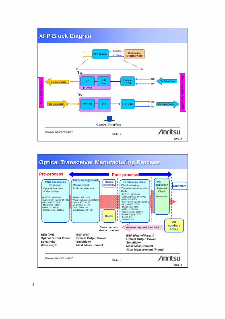
XFP Block DiagramXFP Block Diagram
Rx
Tx
Tx Data InputTx Data Output
Rx Data OutputRx Data InputOpt
ical
Inte
rfac
eElectrical Interface (XFI)
(TOSA)
(ROSA)
XFP Module Host System SERDES/ASIC
LD LD Driver
PIN-PD TIA LIA / CDR
Re-timer / CDR
TD+
TD-
RD+
RD-
Tx Data
Rx Data
Control Interface
Slide 8
2006 10
Optical Transceiver Manufacturing ProcessOptical Transceiver Manufacturing Process
All numbers
check
Repair
Check for non-standard module
Post-processPre-process
ModuleAssembly
Tx/Rx AdjustmentShipment
Optical Features & Mechanism
Parts Acceptance Inspection
Substrate Adjustment/
MeasurementPerformance Check Final
Inspection
Modules returned from field
・BERTS: MP1800A・Wavelength counter:86120C・Optical ATT: 8156・Multimeter: 34401・OPM: MT9810B・Oscilloscope: 86100A
・BERTS: MP1800A・Wavelength counter:86120C・Optical ATT: 8156・Multimeter: 34401・OPM: MT9810B・Oscilloscope: 86100A
・BERTS: MP1800A・Jitter Analyzer: MP1590B・OSA: MS9710C・Wavelength counter: 86120C・Optical ATT: 8156・Multimeter: 34401・OPM: MT9810B・Oscilloscope: 86100A・Power Supply: 6612・Long Fiber(20/40/80 km)
External Check
Checked using Temperature-controlled Bath
Microscope
BER (PN)Optical Output PowerSensitivityWavelength
BER (PN)Optical Output PowerSensitivityMask Measurement
BER (Frame/Margin)Optical Output PowerSensitivityMask MeasurementJitter Measurement (Frame)
5
Slide 9
2006 10
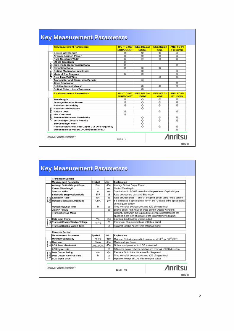
Key Measurement ParametersKey Measurement ParametersTx Measurement Parameters ITU-T G.957
SDH/SONETIEEE 802.3ae
10GbEIEEE 802.3z
GbEANSI FC-PIFC 1G/2G
Center Wavelength
Average Launch Power
RMS Spectrum Width
-20 dB Spectrum
Side-mode Suppression Ratio
Extinction Ratio
Optical Modulation Amplitude
Mask of Eye Diagram
Rise Time/Fall Time
Transmitter and Dispersion Penalty
Jitter Generation
Relative Intensity Noise
Optical Return Loss Tolerance
Rx Measurement Parameters ITU-T G.957SDH/SONET
IEEE 802.3ae10GbE
IEEE 802.3zGbE
ANSI FC-PIFC 1G/2G
Wavelength
Average Receive Power
Receiver Sensitivity
Receiver Reflectance
Return Loss
Min. Overload
Stressed Receiver Sensitivity
Vertical Eye Closure Penalty
Stressed Eye Jitter
Receive Electrical 3 dB Upper Cut Off Frequency
Stressed Receiver DCD Component of DJ
Opt
ical
Out
put
Opt
ical
Inpu
t
Slide 10
2006 10
Key Measurement ParametersKey Measurement ParametersTransmitter SectionMeasurement Parameter Symbol Unit ExplanationAverage Optical Output Power Pout dBm Average Optical Output PowerCenter Wavelength λ nm Center WavelengthSpectral Width σ nm Spectral width of -20dB down from the peak level of optical signalSidemode Suppression Ratio SSR dB Ratio between the peak and Side modeExtinction Ratio ER dB Ratio between Data "1" and "0" of Optical power using PRBS patternOptical Modulation Amplitude OMA μW It is difference in optical power for "1" and "0" levels of the optical signal
using Square patternOptical Rise/Fall Time Tr ps Time to rise/fall between 20% and 80% of Signal levelJitter P-P/RMS ps peak to peak / RMS value at cross point of Optical waveformTransmitter Eye Mask Good/NG test which the required pulse shape characteristics are
specified in the form of a mask of the transmitter eye diagram.Data Input Swing Vin Vpp Electrical Input level for Optical outputTransmit Enable/Disable Voltage VEN/VD V Power-on / Shut-downVoltage of Optical signal
Transmit Disable Assert Time us Transmit Disable Assert Time of Optical signal
Receiver SectionMeasurement Parameter Symbol Unit ExplanationMinimum Sensitivity Rsens dBm Minimum Optical power which measured at 10-12 (or 10-10)BEROverload Pmax dBm Maximum Input PowerLOS Assert/De-Assert LOSA/LOSD dBm Optical input power which LOS is detected
LOS Hysteresis dB Difference power between detction and removal of LOS detectionData Output Swing Vout Vpp Electrical Output Amplitude level for Single endData Output Rise/Fall Time Tr ps Time to rise/fall between 20% and 80% of Signal levelLOS Signal Level V High/Low Voltage of LOS indicate signal output
Opt
ical
Out
put
Elec
tric
alIn
put
Opt
ical
Inpu
tEl
ectr
ical
Out
put

6
Slide 11
2006 10
Key Measurement ParametersKey Measurement Parameters
Rise Time Time to rise from 20% to 80% of signal levelFall Time Time to fall from 80% to 20% of signal levelExtinction ratio Ratio of optical power of “0” and “1” data Jitter Time variation of rising or falling edge of optical waveformMin. Sensitivity Optical power of input signal to achieve 10-10 or 10-12 BER
Test procedure described in IEC61280-2-1, 61280-2-2
Power (dB
m)
Time (ps)
BER
Input optical power (dBm)
Tr Tf
Jitter
Sensitivity
Optical output waveform
10-12
Slide 12
2006 10
1. Center Wavelength2. Spectral Width3. Average Optical Output Power4. Transmitter Eye-Diagram5. Extinction Ratio & OMA6. Minimum Sensitivity7. Jitter
*Reference ITU-T G.957 and IEEE802.3z/ae
Measurement ProceduresMeasurement Procedures

7
Slide 13
2006 10
The maximum spectral width is specified as the maximum full width of the center wavelength peak, measured –20 dB down from the maximum amplitude of the center wavelength.
1. Center Wavelength 2. Spectral Width
E/O
MS9710COptical Spectrum Analyzer
DUT
System Setup
O/E
Data
XData
Wavelength
Power
–20 dBB
A: Center wavelength
B: Max. –20 dB width
A
Measurement ProceduresMeasurement Procedures
MP1800A SQA (PPG)
Slide 14
2006 10
3. Average Optical Output Power
*Point S: The reference point on the optical fiber just after the transmitter optical connector *Point R: The reference point on the optical fiber just before the receiver optical connector.System Setup
MP1800A SQA (PPG)
E/O
MT9810B Optical Power MeterDUT
O/E
Data
XData
Measurement ProceduresMeasurement Procedures
The mean launched power at point S is the averagepower of the transmitter. It is given as a range toallow for some cost optimization and to cover allowances for operation under standard operatingconditions, Tx connector degradations, measurement tolerances, and aging effects. These values allow calculation of values for the sensitivity and overload point for the Rx at point R.

8
Slide 15
2006 10
4. Transmitter Eye-DiagramTransmitter pulse shape characteristics, including rise/fall
times, pulse overshoot/undershoot, and ringing—all of which should be controlled to prevent excessive degradation of the Rx sensitivity—are specified in the form of a mask for the Tx eye-diagram at point S.
The parameters specifying the mask for the Tx eye-diagram are shown in ITU-T G.959 Fig. 7-1.
Measurement ProceduresMeasurement Procedures
G.959.1_F7-1
Mean level of centre oflogical "1"
Mean level of centre oflogical "0"
1+y3
1
y2
0
1
0.5
y1
–y4
0 x2 x3
#1 – Δ is a variable –0.25 < Δ < +0.25.#2 – x2 and x3 of the rectangular eye mask need not be equidistant with respect to the vertical axes at 0 UI and 1 UI.
0.250.250.250.250.25y4
0.250.250.250.40.25y3
0.75Δ + 0.75 (#1)0.750.750.75y2
0.25Δ + 0.25 (#1)0.250.250.25y1
0.20.20.20.20.2x3–x2 (#2)
NRZ 40GNRZ 10G Amplified
NRZ 10G 1550-nm region
NRZ 10G 1310-nm region
NRZ 2.5G
Slide 16
2006 10
Measurement ProceduresMeasurement Procedures
The convention for the optical logic level is: Light emission = logical “1”No emission = logical “0”
EX is defined as: ER = 10 log10(A/B)
OMA is defined as: OMA = A – B
Where, A is the average optical power level for logical “1”and B is the average optical power level for logical “0”.
5. Extinction Ratio & OMA
OM
A
A
B
Average Power
OMA: Optical Modulation Amplitude
ER: Extinction Ratio

9
Slide 17
2006 10
4. Transmitter Eye-Diagram5. Extinction Ratio & OMA
System Setup
E/O
MP1026AEye Pattern Analyzer
(Sampling Oscilloscope)DUT
O/ETrigger
Data
XData
Measurement ProceduresMeasurement Procedures
MP1800A SQA (PPG)
P
Slide 18
2006 10
Measurement ProceduresMeasurement Procedures
Average optical power (or OMA)vs. BER
The minimum sensitivity level for receiver section is obtained from this graph.
Min Sensitivity: Min Sensitivity: ––24.68 dBm at BER 1E24.68 dBm at BER 1E--1010
6. Minimum SensitivityReceiver sensitivity is defined as the minimum acceptable value of average received power at point R to achieve BER 1E–10 (or 1E–12).
*It takes into account power penalties caused by use of a transmitter under standard operating conditions with worst-case values for extinction ratio, pulse rise/fall times, optical return loss at point S, Rx connector degradations and measurement tolerances.

10
Slide 19
2006 10
6. Minimum SensitivitySystem Setup
GoldenE/O
MT9810BOptical Power Meter
Optical Attenuator
O/E
DUT
Data
XData
Data
E/O
Coupler
Measurement ProceduresMeasurement Procedures
MP1800A SQA
Optical Interface
or Electrical Interface
Slide 20
2006 10
Measurement ProceduresMeasurement Procedures
Type of Jitter measurement
GeneralMeasure Mask of Eye Diagram and time variation of the rising/falling edge of signal using Oscilloscope.
ITU-T baseMeasure Jitter Generation/Tolerance/Transfer and Output Jitter using Jitter Analyzer
IEEE base (Stressed Eye)Stressed Receiver Conformance Test
7. Jitter measurement
11
Slide 21
2006 10
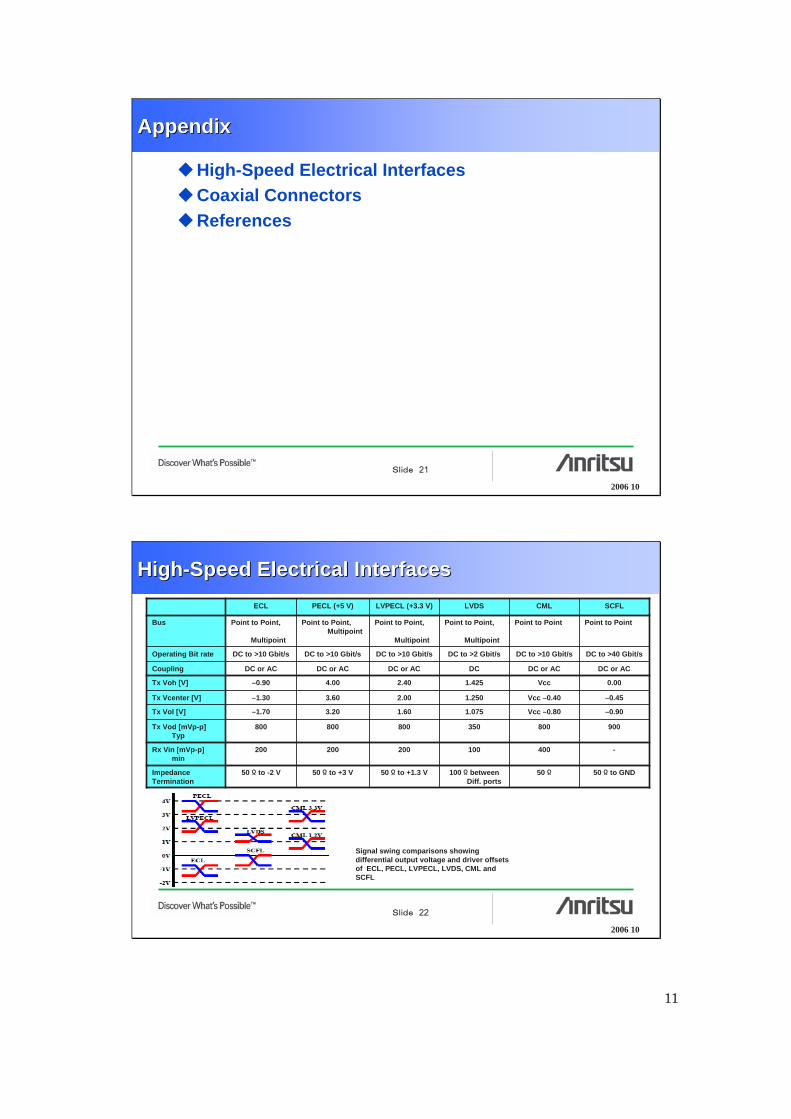
AppendixAppendix
High-Speed Electrical InterfacesCoaxial ConnectorsReferences
Slide 22
2006 10
HighHigh--Speed Electrical InterfacesSpeed Electrical Interfaces
-400100200200200Rx Vin [mVp-p]min
50 Ω to GND50 Ω100 Ω between Diff. ports
50 Ω to +1.3 V50 Ω to +3 V50 Ω to -2 VImpedance Termination
900 800 350 800 800 800 Tx Vod [mVp-p] Typ
–0.90 Vcc –0.801.075 1.60 3.20 –1.70 Tx Vol [V]
–0.45 Vcc –0.401.250 2.00 3.60 –1.30 Tx Vcenter [V]
0.00 Vcc1.425 2.40 4.00 –0.90 Tx Voh [V]
DC or ACDC or ACDC DC or ACDC or ACDC or ACCoupling
DC to >40 Gbit/sDC to >10 Gbit/sDC to >2 Gbit/sDC to >10 Gbit/sDC to >10 Gbit/sDC to >10 Gbit/sOperating Bit rate
Point to PointPoint to PointPoint to Point,
Multipoint
Point to Point,
Multipoint
Point to Point,Multipoint
Point to Point,
Multipoint
Bus
SCFLCMLLVDSLVPECL (+3.3 V)PECL (+5 V)ECL
Signal swing comparisons showing differential output voltage and driver offsets of ECL, PECL, LVPECL, LVDS, CML and SCFL
12
Slide 23
2006 10
HighHigh--Speed Electrical InterfacesSpeed Electrical Interfaces
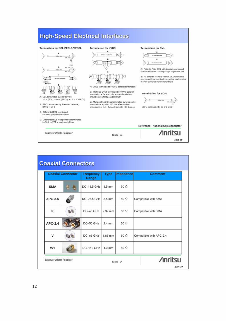
Termination for ECL/PECL/LVPECL
A: ECL terminated by 50 Ω to VTT; –2 V (ECL), +3.0 V (PECL), +1.3 V (LVPECL)
B: PECL terminated by Thevenin network, R1/R2 = 50 Ω
C: Differential ECL terminated by 100 Ω parallel termination
D: Differential ECL Multipoint bus terminated by 50 Ω to VTT at each end of bus
C
Termination for CML
A: Point-to-Point CML with internal source and load terminations—50 Ω pull-ups to positive rail
B: AC coupled Point-to-Point CML with internal source and load terminations—driver and receiver may be powered from different rails
Termination for SCFL
SCFL terminated by 50 Ω to GND
Termination for LVDS
A: LVDS terminated by 100 Ω parallel termination
B: Multidrop LVDS terminated by 100 Ω parallel termination at far end only; stubs off main line should be shortest possible length
C: Multipoint LVDS bus terminated by two parallel terminations equal to 100 Ω or effective load impedance of bus—typically in 54 to 100 Ω range
Reference: National Semiconductor
Slide 24
2006 10
Coaxial ConnectorsCoaxial Connectors
1.0 mm
1.85 mm
2.4 mm
2.92 mm
3.5 mm
3.5 mm
Type
50 ΩDC–50 GHzAPC-2.4
50 ΩDC–110 GHzW1
Compatible with APC-2.450 ΩDC–65 GHzV
Compatible with SMA50 ΩDC–40 GHzK
Compatible with SMA50 ΩDC–26.5 GHzAPC-3.5
50 ΩDC–18.5 GHzSMA
CommentImpedanceFrequency Range
Coaxial Connector

13
Slide 25
2006 10
ReferencesReferences
http://www.300pinmsa.org300pinhttp://www.qsfpmsa.org/QSFPhttp://www.xenpak.org/XENPAKhttp://www.x2msa.org/X2http://www.xpak.org/XPAKhttp://www.xfpmsa.org/cgi-bin/home.cgiXFPhttp://schelto.com/SFP/SFF/sff.htmSFFhttp://schelto.com/SFP/index.htmlSFPhttp://MSA
Slide 26
2006 10
ENDEND

Anritsu Corporation5-1-1 Onna, Atsugi-shi, Kanagawa, 243-8555 JapanPhone: +81-46-223-1111Fax: +81-46-296-1264
• U.S.A.Anritsu Company1155 East Collins Blvd., Suite 100, Richardson, TX 75081, U.S.A.Toll Free: 1-800-267-4878Phone: +1-972-644-1777Fax: +1-972-671-1877
• CanadaAnritsu Electronics Ltd.700 Silver Seven Road, Suite 120, Kanata, Ontario K2V 1C3, CanadaPhone: +1-613-591-2003 Fax: +1-613-591-1006
• Brazil Anritsu Eletrônica Ltda.Praca Amadeu Amaral, 27 - 1 Andar01327-010-Paraiso-São Paulo-BrazilPhone: +55-11-3283-2511Fax: +55-11-3288-6940
• U.K.Anritsu EMEA Ltd.200 Capability Green, Luton, Bedfordshire, LU1 3LU, U.K.Phone: +44-1582-433200 Fax: +44-1582-731303
• FranceAnritsu S.A.9 Avenue du Québec, Z.A. de Courtabœuf 91951 Les Ulis Cedex, France Phone: +33-1-60-92-15-50Fax: +33-1-64-46-10-65
• GermanyAnritsu GmbHNemetschek Haus, Konrad-Zuse-Platz 1 81829 München, Germany Phone: +49-89-442308-0 Fax: +49-89-442308-55
• ItalyAnritsu S.p.A.Via Elio Vittorini 129, 00144 Roma, ItalyPhone: +39-6-509-9711 Fax: +39-6-502-2425
• SwedenAnritsu ABBorgafjordsgatan 13, 164 40 KISTA, SwedenPhone: +46-8-534-707-00 Fax: +46-8-534-707-30
• FinlandAnritsu ABTeknobulevardi 3-5, FI-01530 VANTAA, FinlandPhone: +358-20-741-8100Fax: +358-20-741-8111
• DenmarkAnritsu A/SKirkebjerg Allé 90, DK-2605 Brøndby, DenmarkPhone: +45-72112200Fax: +45-72112210
• SpainAnritsu EMEA Ltd. Oficina de Representación en EspañaEdificio VeganovaAvda de la Vega, n˚ 1 (edf 8, pl 1, of 8)28108 ALCOBENDAS - Madrid, SpainPhone: +34-914905761Fax: +34-914905762
• United Arab EmiratesAnritsu EMEA Ltd.Dubai Liaison OfficeP O Box 500413 - Dubai Internet CityAl Thuraya Building, Tower 1, Suit 701, 7th FloorDubai, United Arab EmiratesPhone: +971-4-3670352Fax: +971-4-3688460
• SingaporeAnritsu Pte. Ltd.10, Hoe Chiang Road, #07-01/02, Keppel Towers,Singapore 089315 Phone: +65-6282-2400 Fax: +65-6282-2533
• IndiaAnritsu Pte. Ltd. India Branch OfficeUnit No. S-3, Second Floor, Esteem Red Cross Bhavan,No. 26, Race Course Road, Bangalore 560 001, IndiaPhone: +91-80-32944707Fax: +91-80-22356648
• P.R. China (Hong Kong)Anritsu Company Ltd.Units 4 & 5, 28th Floor, Greenfield Tower, Concordia Plaza, No. 1 Science Museum Road, Tsim Sha Tsui East,Kowloon, Hong KongPhone: +852-2301-4980Fax: +852-2301-3545
• P.R. China (Beijing)Anritsu Company Ltd.Beijing Representative OfficeRoom 1515, Beijing Fortune Building, No. 5, Dong-San-Huan Bei Road, Chao-Yang District, Beijing 10004, P.R. ChinaPhone: +86-10-6590-9230Fax: +86-10-6590-9235
• KoreaAnritsu Corporation, Ltd.8F Hyunjuk Building, 832-41, Yeoksam Dong, Kangnam-ku, Seoul, 135-080, KoreaPhone: +82-2-553-6603Fax: +82-2-553-6604
• AustraliaAnritsu Pty. Ltd.Unit 21/270 Ferntree Gully Road, Notting Hill, Victoria 3168, AustraliaPhone: +61-3-9558-8177Fax: +61-3-9558-8255
• TaiwanAnritsu Company Inc.7F, No. 316, Sec. 1, Neihu Rd., Taipei 114, TaiwanPhone: +886-2-8751-1816Fax: +886-2-8751-1817
Specifications are subject to change without notice.
No. MP1800A-E-F-1-(1.00) Printed in Japan 2007-5 AKD
Please Contact:
070207
Printed on 70% Recycled Paper
公知