Application Note: AZD068 A short guide on trackpad layoutThe design of a trackpad generally consists...
10
IQ Switch ® ProxSense ® Series Copyright © Azoteq (Pty) Ltd Page 1 of 10 All Rights Reserved. Revision 2 July 2016 Application Note: AZD068 A short guide on trackpad layout Contents 1. Introduction ................................................................................................................................ 1 2. Develop sensor pattern using CAD software .............................................................................. 2 2.1. Sensors/Channels ................................................................................................................ 2 2.2. Gap between diamonds ...................................................................................................... 2 2.3. Spacing/pitch inside pattern ............................................................................................... 2 2.4. Ground ring ......................................................................................................................... 3 2.5. Sensitivity ............................................................................................................................ 3 2.6. Active area .......................................................................................................................... 3 2.7. Metal domes ....................................................................................................................... 4 2.8. PCBs with arbitrary outlines................................................................................................ 5 3. Finalise trackpad in PCB editor ................................................................................................... 5 3.1. Shielding .............................................................................................................................. 5 3.2. Typical IC placement and routing ....................................................................................... 6 3.3. Connections at metal dome footprints ............................................................................... 7 3.4. Ground ................................................................................................................................ 7 4. Mechanical stackup considerations ............................................................................................ 8 4.1 Airgaps ................................................................................................................................ 8 4.2 Isolation sheets ................................................................................................................... 9 5. Contact Information...................................................................................................................... 10 1. Introduction This document provides the reader with a brief overview of important aspects that one should be aware of when designing a trackpad. A more comprehensive document on the subject is available on request from Azoteq ([email protected]). The design of a trackpad generally consists of two activities: o Develop a sensor pattern using CAD software. o Import the sensor pattern into a PCB editor, finalise the wire routing and export the manufacturing files.
Transcript of Application Note: AZD068 A short guide on trackpad layoutThe design of a trackpad generally consists...

IQ Switch®
ProxSense® Series
Copyright © Azoteq (Pty) Ltd Page 1 of 10
All Rights Reserved. Revision 2 July 2016
Application Note: AZD068 A short guide on trackpad layout
Contents 1. Introduction ................................................................................................................................ 1
2. Develop sensor pattern using CAD software .............................................................................. 2
2.1. Sensors/Channels ................................................................................................................ 2
2.2. Gap between diamonds ...................................................................................................... 2
2.3. Spacing/pitch inside pattern ............................................................................................... 2
2.4. Ground ring ......................................................................................................................... 3
2.5. Sensitivity ............................................................................................................................ 3
2.6. Active area .......................................................................................................................... 3
2.7. Metal domes ....................................................................................................................... 4
2.8. PCBs with arbitrary outlines ................................................................................................ 5
3. Finalise trackpad in PCB editor ................................................................................................... 5
3.1. Shielding .............................................................................................................................. 5
3.2. Typical IC placement and routing ....................................................................................... 6
3.3. Connections at metal dome footprints ............................................................................... 7
3.4. Ground ................................................................................................................................ 7
4. Mechanical stackup considerations ............................................................................................ 8
4.1 Airgaps ................................................................................................................................ 8
4.2 Isolation sheets ................................................................................................................... 9
5. Contact Information ...................................................................................................................... 10
1. Introduction This document provides the reader with a brief overview of important aspects that one should be
aware of when designing a trackpad. A more comprehensive document on the subject is available
on request from Azoteq ([email protected]).
The design of a trackpad generally consists of two activities:
o Develop a sensor pattern using CAD software.
o Import the sensor pattern into a PCB editor, finalise the wire routing and export the
manufacturing files.

IQ Switch®
ProxSense® Series
Copyright © Azoteq (Pty) Ltd Page 2 of 10
All Rights Reserved. Revision 2 July 2016
2. Develop sensor pattern using CAD software The following subsections describe the various aspects that should be considered when creating a
sensor pattern using CAD software.
2.1. Sensors/Channels
A trackpad is a two-dimensional array of sensors. Each sensor consists of a TX conductor and a RX
conductor that are in close proximity. Refer to Figure 1 for an illustration of a sensor and of a
trackpad.
(a) Sensor/Channel (b) Trackpad
Figure 1: Arrangement of sensors in a trackpad.
2.2. Gap between diamonds
The gap between the TX and RX electrodes determines how far a signal is projected as well as the
level of noise in the measured signal. A sensor with a larger gap will be able to detect a user further
away but will have more noise than a sensor with a smaller gap. Typical gap dimensions are
provided in Table 1.
Table 1: Gap between TX and RX electrodes
Minimum Typical Maximum
Gap 0.1mm 0.3mm 0.5mm
2.3. Spacing/pitch inside pattern
The distance between the sensors in a trackpad is referred to as the pitch. The pitch determines the
range of finger sizes that can reliably be detected by the trackpad. The minimum finger diameter is
approximately equal to √𝑥𝑃𝑖𝑡𝑐ℎ2 + 𝑦𝑃𝑖𝑡𝑐ℎ2. Typical dimensions for the pitch of a trackpad are
provided in Table 2.
IQ Switch®
ProxSense® Series
Copyright © Azoteq (Pty) Ltd Page 3 of 10
All Rights Reserved. Revision 2 July 2016
Table 2: Sensor pitch: Distance between sensors in trackpad.
Minimum Typical Maximum
Pitch 4mm 5-7 mm 8mm
2.4. Ground ring
It is good practise to place an exposed (not covered by solder mask) ground ring around the
trackpad. The ring can be placed on multiple layers and connected using vias to avoid building a
loop antenna. The purpose of the ring is to provide ESD protection. Care should be taken to ensure
that the minimum copper clearance at the board edge, as determined by the relevant manufacturing
process, is adhered to.
Figure 2: Illustration of a ground ring around a trackpad pattern.
2.5. Sensitivity
The sensitivity of a trackpad is not uniform over the entire surface of the sensor pattern. An
illustration of the sensitivity of a trackpad is provided in Figure 3 (b).
2.6. Active area
The active area of a trackpad is the area for which X and Y coordinates are reported. It starts at the
centre of the first channel in the first row and ends at the centre of the last channel in the last row.
An illustration of the active area is provided in Figure 3 (a). Note that there is always a dead band
around a trackpad that cannot be used. The dead band becomes smaller as the pitch is decreased.

IQ Switch®
ProxSense® Series
Copyright © Azoteq (Pty) Ltd Page 4 of 10
All Rights Reserved. Revision 2 July 2016
(a) (b)
Figure 3: An illustration of the active area of a trackpad is shown in (a) and an illustration of the change in sensor sensitivity over the trackpad is shown in (b). Red is areas of high sensitivity and green is areas of lower sensitivity.
2.7. Metal domes
Metal domes can be placed on the sensor pattern and the action of depressing them can be
detected (as the channel snap output). The metal dome should be positioned in such a way that it
partially covers both a RX and a TX. The conductors must be covered by solder mask so that it is
impossible for the metal dome to form a short-circuit between the TX and the RX electrodes. It is
also good practice to add a thin (~0.1mm) single-sided adhesive tape over the sensor area. The
placement of a metal dome on a trackpad will always degrade the performance of the trackpad. It is
however possible to minimise the interference caused by the metal dome by positioning the domes
at suitable locations. Suitable metal dome locations are shown in Figure 4.
(a) (b) ( c)
Figure 4: Possible metal dome positions on a diamond pattern arranged from best to worse. The best location is shown in (a). Note that the arrangement shown in (c) should still result in a trackpad with acceptable performance.
The typical sensor dimensions for a metal dome with a diameter of 4mm are provided in Figure 5 (a).
A metal dome can have any shape or size. It is advisable to use the smallest possible metal dome
that still provides adequate haptic feedback to the user. This is because the metal dome blocks
some of the fields around the sensor and a smaller dome has a smaller effect. If the metal dome is
positioned on top of a single diamond, as shown in Figure 4 (a) and (b), the best course of action is to
change the shape of the diamonds in the area so that the diamond beneath the metal dome still has
some area that is not entirely covered by the dome. This concept is illustrated in Figure 4 (b) and
Figure 5 (b).

IQ Switch®
ProxSense® Series
Copyright © Azoteq (Pty) Ltd Page 5 of 10
All Rights Reserved. Revision 2 July 2016
(a) (b)
Figure 5: Dimensions for a typical metal dome button is provided in (a) and an illustration of a non-standard metal dome button is provided in (b).
2.8. PCBs with arbitrary outlines
A trackpad can have any arbitrary outline. It is however advisable to use a rectangular shape as this
ensures that all of the channels on the edges have the same copper area and therefore similar
sensitivity. Figure 6 shows the channels on a round trackpad. Channels 5 and 2 are almost non-
existent and will not be very sensitive.
Figure 6: Diamond pattern for a round trackpad. Channels 5 and 2 will not be very sensitive and will probably have to be disabled.
3. Finalise trackpad in PCB editor A sensor pattern that was created using CAD software can be exported as a DXF-file and imported
into a PCB editor. The following subsections discuss the routing of the electrical connections and the
placement of the IC.
3.1. Shielding
As mentioned earlier, a sensor is formed when a TX track is positioned in close proximity to a RX
track. It follows that TX and RX tracks should be routed separately and should only come in close
proximity at the actual sensor. TX and RX tracks should always be shielded from each other using
ground, and should only cross each other at 90˚ angles to minimise the cross-coupling. These
concepts are illustrated in Figure 7.
Φ4mm metal dome Φ2m
m VIA
Φ3mm

IQ Switch®
ProxSense® Series
Copyright © Azoteq (Pty) Ltd Page 6 of 10
All Rights Reserved. Revision 2 July 2016
(a) (b)
Figure 7: RX and TX tracks should be shielded from each other using ground (a). When a TX and a RX track have to cross, it is preferable to cross the tracks at 90˚ to minimise the coupling.
3.2. Typical IC placement and routing
The IC can be positioned beneath the trackpad or outside of the trackpad. If the IC is positioned
outside of the trackpad, the performance of the sensor will be better, but the sensing area will be
smaller. The patterns shown in Figure 8 (a) and (b) provide the best results as they minimise
unwanted cross-coupling. The pattern in Figure 8 (c) results in the largest sensor area (for a fixed
PCB size), followed by the pattern in (b) and then that in (a). The pattern in Figure 8 (b) provides a
good trade-off between sensor size and trackpad performance. In Figure 8 (c) it is important to note
that TX tracks can only be routed beneath TX diamonds and RX tracks can only be routed beneath RX
diamonds. Whenever a TX track is beneath a RX diamond, or a RX track is beneath a TX diamond,
the diamond has to be cut to remove the parallel TX-RX section.
(a) (b) ( c)
Figure 8: Typical routing patterns for cases where the IC is positioned outside of the trackpad area. RXs are blue, TXs are red and ground is green. The pattern in ( c) has the largest sensor area, followed by (b) and then (a).
IQ Switch®
ProxSense® Series
Copyright © Azoteq (Pty) Ltd Page 7 of 10
All Rights Reserved. Revision 2 July 2016
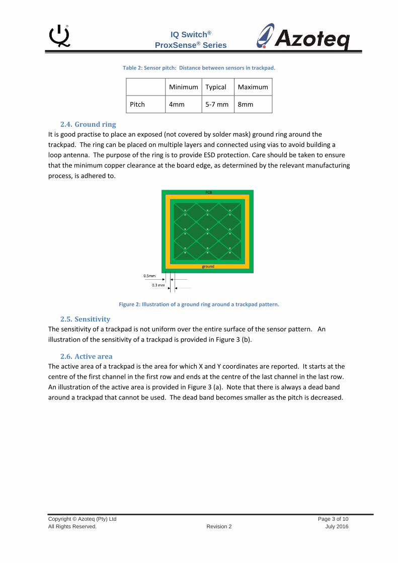
Figure 9: Advised routing pattern for situations where the IC has to be positioned beneath the trackpad area. Note that for a two-layer board the pitch cannot be smaller than the width/length of the IC.
In situations where the IC has to be located beneath the trackpad area, it is advisable to follow the
pattern illustrated in Figure 9. Here the IC is positioned in such a manner that the maximum number
of RX pins are located beneath a RX diamond and the maximum number of TX pins are located
beneath a TX diamond. Again, TX tracks are only allowed to be routed beneath TX diamonds and RX
tracks are only allowed to be routed beneath RX diamonds.
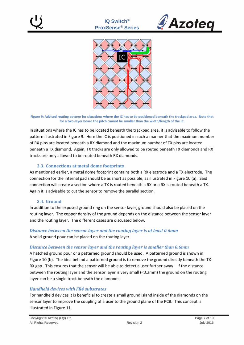
3.3. Connections at metal dome footprints
As mentioned earlier, a metal dome footprint contains both a RX electrode and a TX electrode. The
connection for the internal pad should be as short as possible, as illustrated in Figure 10 (a). Said
connection will create a section where a TX is routed beneath a RX or a RX is routed beneath a TX.
Again it is advisable to cut the sensor to remove the parallel section.
3.4. Ground
In addition to the exposed ground ring on the sensor layer, ground should also be placed on the
routing layer. The copper density of the ground depends on the distance between the sensor layer
and the routing layer. The different cases are discussed below.
Distance between the sensor layer and the routing layer is at least 0.6mm
A solid ground pour can be placed on the routing layer.
Distance between the sensor layer and the routing layer is smaller than 0.6mm
A hatched ground pour or a patterned ground should be used. A patterned ground is shown in
Figure 10 (b). The idea behind a patterned ground is to remove the ground directly beneath the TX-
RX gap. This ensures that the sensor will be able to detect a user further away. If the distance
between the routing layer and the sensor layer is very small (<0.2mm) the ground on the routing
layer can be a single track beneath the diamonds.
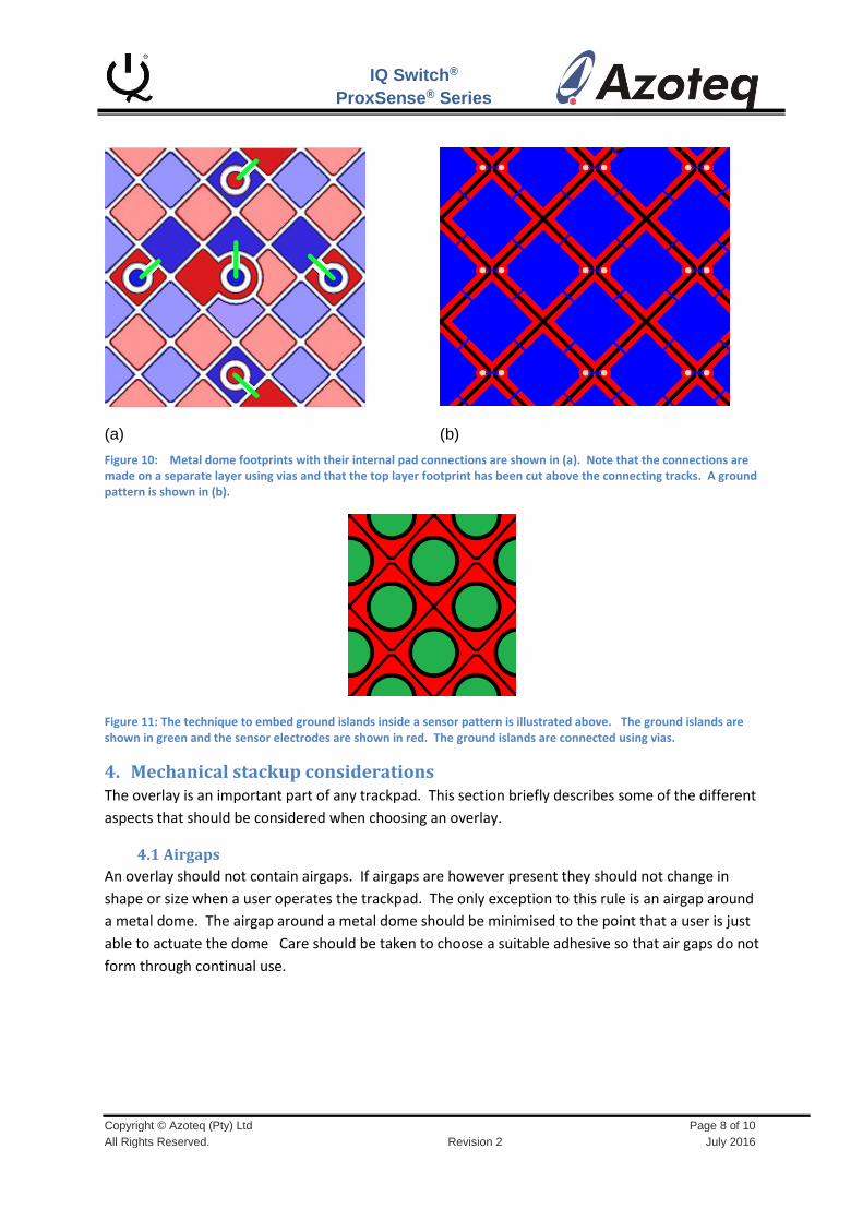
Handheld devices with FR4 substrates
For handheld devices it is beneficial to create a small ground island inside of the diamonds on the
sensor layer to improve the coupling of a user to the ground plane of the PCB. This concept is
illustrated in Figure 11.
IQ Switch®
ProxSense® Series
Copyright © Azoteq (Pty) Ltd Page 8 of 10
All Rights Reserved. Revision 2 July 2016
(a) (b)
Figure 10: Metal dome footprints with their internal pad connections are shown in (a). Note that the connections are made on a separate layer using vias and that the top layer footprint has been cut above the connecting tracks. A ground pattern is shown in (b).
Figure 11: The technique to embed ground islands inside a sensor pattern is illustrated above. The ground islands are shown in green and the sensor electrodes are shown in red. The ground islands are connected using vias.
4. Mechanical stackup considerations The overlay is an important part of any trackpad. This section briefly describes some of the different
aspects that should be considered when choosing an overlay.
4.1 Airgaps
An overlay should not contain airgaps. If airgaps are however present they should not change in
shape or size when a user operates the trackpad. The only exception to this rule is an airgap around
a metal dome. The airgap around a metal dome should be minimised to the point that a user is just
able to actuate the dome Care should be taken to choose a suitable adhesive so that air gaps do not
form through continual use.

IQ Switch®
ProxSense® Series
Copyright © Azoteq (Pty) Ltd Page 9 of 10
All Rights Reserved. Revision 2 July 2016
4.2 Isolation sheets
If a PCB design contains metal domes on a trackpad, it is good practice to place a PET isolation sheet
between the PCB and the metal dome sticker. The use of an isolation sheet has the following
distinct advantages:
o Increases the durability of the buttons (prevents a short-circuit due to continual use).
o Decreases the sensitivity to production variation of metal dome parameters (size, actuating
force, etc.).
Table 3 contains recommendations for isolation sheet thicknesses.
Table 3: Recommendation for isolation sheet thickness.
Minimum Typical Maximum
Sheet thickness 0.1mm 0.14 mm 0.2mm
Values are subject to the size and position of the metal domes on the diamond pattern, as well as the gap between diamonds. Larger domes and/or larger gaps between diamonds require thicker isolation sheets.

IQ Switch®
ProxSense® Series
Copyright © Azoteq (Pty) Ltd Page 10 of 10
All Rights Reserved. Revision 2 July 2016
5. Contact Information
USA Asia South Africa
Physical
Address
6507 Jester Blvd Bldg 5, suite 510G Austin TX 78750 USA
Rm2125, Glittery City
Shennan Rd
Futian District
Shenzhen, 518033
China
109 Main Street
Paarl
7646
South Africa
Postal
Address 6507 Jester Blvd
Bldg 5, suite 510G
Austin
TX 78750
USA
Rm2125, Glittery City
Shennan Rd
Futian District
Shenzhen, 518033
China
PO Box 3534
Paarl
7620
South Africa
Tel +1 512 538 1995 +86 755 8303 5294
ext 808
+27 21 863 0033
Fax +1 512 672 8442 +27 21 863 1512
Email [email protected] [email protected] [email protected]
Please visit www.azoteq.com for a list of distributors and worldwide representation.
The following patents relate to the device or usage of the device: US 6,249,089 B1; US 6,621,225 B2; US 6,650,066 B2; US 6,952,084
B2; US 6,984,900 B1; US 7,084,526 B2; US 7,084,531 B2; US 7,265,494 B2; US 7,291,940 B2; US 7,329,970 B2; US 7,336,037 B2; US 7,443,101
B2; US 7,466,040 B2 ; US 7,498,749 B2; US 7,528,508 B2; US 7,755,219 B2; US 7,772,781 B2; US 7,781,980 B2; US 7,915,765 B2; US
7,994,726 B2; US 8,035,623 B2; US RE43,606 E; US 8,288,952 B2; US 8,395,395 B2; US 8,531,120 B2; US 8,659,306 B2; US 8,823,273 B2; EP 1
120 018 B2; EP 1 206 168 B1; EP 1 308 913 B1; EP 1 530 178 A1; EP 2 351 220 B1; EP 2 559 164 B1; CN 1330853; CN 1783573; AUS 761094;
HK 104 1401
IQ Switch®, SwipeSwitch™, ProxSense®, LightSense™, AirButtonTM, ProxFusion™, Crystal Driver™ and the logo are
trademarks of Azoteq.
The information in this Datasheet is believed to be accurate at the time of publication. Azoteq uses reasonable effort to maintain the information up-to-date and accurate, but does not warrant the accuracy,
completeness or reliability of the information contained herein. All content and information are provided on an “as is” basis only, without any representations or warranties, express or implied, of any kind,
including representations about the suitability of these products or information for any purpose. Azoteq disclaims all warranties and conditions with regard to these products and information, including but not
limited to all implied warranties and conditions of merchantability, fitness for a particular purpose, title and non-infringement of any third party intellectual property rights. Azoteq assumes no liability for any
damages or injury arising from any use of the information or the product or caused by, without limitation, failure of performance, error, omission, interruption, defect, delay in operation or transmission, even if
Azoteq has been advised of the possibility of such damages. The applications mentioned herein are used solely for the purpose of illustration and Azoteq makes no warranty or representation that such
applications will be suitable without further modification, nor recommends the use of its products for application that may present a risk to human life due to malfunction or otherwise. Azoteq products are not
authorized for use as critical components in life support devices or systems. No licenses to patents are granted, implicitly, express or implied, by estoppel or otherwise, under any intellectual property rights. In
the event that any of the abovementioned limitations or exclusions does not apply, it is agreed that Azoteq’s total liability for all losses, damages and causes of action (in contract, tort (including without
limitation, negligence) or otherwise) will not exceed the amount already paid by the customer for the products. Azoteq reserves the right to alter its products, to make corrections, deletions, modifications,
enhancements, improvements and other changes to the content and information, its products, programs and services at any time or to move or discontinue any contents, products, programs or services without
prior notification. For the most up-to-date information and binding Terms and Conditions please refer to www.azoteq.com.
www.azoteq.com/ip