APPENDIX C. SITE REPORTS - WTEC: What's · Web viewAPPENDIX C. SITE REPORTS. Site: Fujitsu ......
55
155 APPENDIX C. SITE REPORTS Site: Fujitsu (Yamagata Plant) 1-6-1 Marunouchi, Chiyoda-Ku, Tokyo 100, Japan Date Visited: October 6, 1993 Report Author: M. Pecht ATTENDEES JTEC: P. Barela W. Boulton G. Harman G. Meieran M. Pecht HOSTS: C. Handa President, Yamagata Fujitsu T. Tsuchimoto Board Director, General Manager of Technology Group, Kawasaki Facility M. Nakazono Director and General Manager, Yamagata Fujitsu BACKGROUND Fujitsu manufactures and automates to the level needed to reduce costs and improve quality incrementally; nothing more, nothing less. Our JTEC group spent a half day at Yamagata Fujitsu (Fujitsu’s Yamagata plant). The main technology that we came to see was
-
Upload
nguyentram -
Category
Documents
-
view
216 -
download
2
Transcript of APPENDIX C. SITE REPORTS - WTEC: What's · Web viewAPPENDIX C. SITE REPORTS. Site: Fujitsu ......

155
APPENDIX C. SITE REPORTS
Site: Fujitsu (Yamagata Plant)1-6-1 Marunouchi, Chiyoda-Ku,Tokyo 100, Japan
Date Visited: October 6, 1993
Report Author: M. Pecht
ATTENDEES
JTEC:
P. BarelaW. BoultonG. HarmanG. MeieranM. Pecht
HOSTS:
C. Handa President, Yamagata FujitsuT. Tsuchimoto Board Director, General Manager of Technology
Group, Kawasaki FacilityM. Nakazono Director and General Manager, Yamagata Fujitsu
BACKGROUND
Fujitsu manufactures and automates to the level needed to reduce costs and improve quality incrementally; nothing more, nothing less.
Our JTEC group spent a half day at Yamagata Fujitsu (Fujitsu’s Yamagata plant). The main technology that we came to see was Fujitsu’s high-volume surface mount operations that are part of its manufacturing process for hard disk drives used in PCs and workstations. We were greeted by Chiaki Handa, President of the Yamagata plant, and by T. Tsuchimoto, Board Director and General Manager of the Technology Group at the Kawasaki Facility, who gave a general overview of the operations of Fujitsu. Then M. Nakazono, Director and General Manager of the Yamagata plant, gave the Yamagata plant overview. Altogether there were 12 managers from three different Fujitsu facilities (Yamagata, Kawasaki, and Atsugi).
Fujitsu has some 71 overseas manufacturing and assembly-and-repair subsidiaries, in addition to numerous sales and other offices. It currently lists 161,974 employees worldwide. (This number does not include employees from Amdahl and other similar affiliates in Europe.) In
Patricia M.H. Johnson, 01/03/-1,
Fujitsu’s revisions did not specifically note this heading, but did target all other mentions of “Fujitsu, Yamagata plant” for change to Yamagata Fujitsu

Appendix C. Site Reports
addition to manufacturing computers, Fujitsu has entered the multimedia market and has been chosen by U.S. common carriers for broadband ISDN equipment, switching systems, optical transmission systems, and cellular mobile phones; it is offering similar equipment in parts of Asia, Australia, and Europe. It is also moving into software and other computer services around the world.
YAMAGATA FUJITSU
Yamagata Fujitsu is located in Japan’s industrial district. Established in 1983, it had 100% investment by Fujitsu; 70% of sales go overseas. As of the JTEC visit, approximately 300 of 1,000 employees were staff, approximately 700 were operators; about 60% were male and 40% female; their average age was 24. The plant developed, produced, and managed sales of disk drives. The JTEC group toured the printed circuit board (PCB) assembly line (PCA) for 3-1/2 inch disk drives and the 2-1/2 inch hard disk drive assembly line (HDA).
Printed Circuit Assembly Line for 3-1/2 Inch Disk Drives
Yamagata Fujitsu’s PCA line incorporates traditional semiautomatic component placement, soldering, and cleaning equipment with manual part and assembly feeding of machines. There was some manual part soldering and a lot of manual inspection, testing, and repair. The reasons given for all the manual work were (1) it was the most cost-effective considering the mix of PCA technologies they needed to handle, (2) there were many odd parts, such as special connectors and heat sinks that didn't easily lend themselves to automation, and (3) product demand was low, so that only two shifts were needed and further automation would not pay off. Over 600 pieces per minute could be manufactured. The components were predominantly plastic. Generally 60% of the boards were composed of SMT; 20% of these were single-sided and double-sided boards, 45% were four-layer, 30% were six-layer, and 5% were eight layers and up. In general the PCA process line was not by any means state-of-the-art and may not even be highly profitable. It was stated that the demand for these products was down.
The 3-1/2 inch drive had a lot of manual handling: for insertion of some components, for rework, and for inspection. Burn-in equipment at the plant operates under the following conditions:
· There are some fans covered with stainless steel mesh at the bottom of this equipment to circulate the inside air.
· There are no heaters inside the equipment. As a number of hard disk drives are operating within a closed box, temperature inside the box increases significantly because of heat radiation from the disk drives. As a consequence, all hard drives kept in the box are burned-in under this high temperature even with no heaters.
· In case of a perfectly sealed system, temperature becomes too high, so, a slit is put on the top side to maintain the hard disk drive's temperature at a range between 67oC and 73oC. The location and size of this slit are based on Fujitsu's know-how.
156
Patricia M.H. Johnson, 01/03/-1,
Delete reference to other products per Kameya letter
Patricia M.H. Johnson, 01/03/-1,
Change site name per Kameya of Fujitsu, letter dated 9/12/94

Appendix C. Site Reports
The cleaning operation was OK, but there was so much handling after the cleaning with bare hands that it seemed as if the cleaning was somewhat superfluous. Of some special interest in the PCA manufacturing line was the removal of CFCs in October 1993 and the subsequent use of non-CFCs, replaced by a deionized water cleaning process. While there was no research being conducted in leadless solder, management was aware of efforts in Germany and did look at InSn, but considered it too expensive.
The small FR-4 boards (to be mounted in hard drives) were demarked and partially cut out but remained in the larger mother boards for handling. Each mother board contained four or six smaller active boards. They were loaded with pick-and-place machines (said to have a placement accuracy of 50 µm — at other sites we saw machines that were more accurate, but 50 µm was apparently adequate for the purpose). The boards were reflow soldered.
In summary, the printed circuit line for 3-1/2 inch discs was "low tech": the machinery was old; the process was a combination of automated and manual assembly; there was lots of inspection; cleanliness was minimal; the burn-in was primitive. It was clear, however, that the important processes were well developed, and all the things we saw that seemed "low-tech" were indeed relatively unimportant (e.g., the burn-in caught what it needed to catch, and having a more sophisticated burn-in system was unnecessary, and hence no attention was paid to it). Thus, the operation appeared efficient for what it was doing, even though it was not elegant. It was obvious that Fujitsu has no intention of significantly improving this line. It was also obvious that Fujitsu was going to use what it learned on this line to make a step-wise improvement on its 2-1/2 inch drive assembly.
It should be noted that the Yamagata plant is dedicated to manufacturing products for personal use, different from any other Fujitsu plant, such as its Numazu plant, which manufactures high-technology products. The main focus of the Yamagata plant is to utilize the existing equipment to a maximum extent to promptly manufacture high-quality products and at the same time to seek better production efficiency at a lower cost.
As pointed out to the JTEC team, the Yamagata plant uses traditional manufacturing methods through semiautomated equipment and manual work on its printed circuit board assembly lines. While installed machines at the Yamagata plant such as screen-printer, parts-mounter, and air-reflow oven may be obsolete from the technical point of view and give the impression that the Yamagata plant continues to use old equipment, our hosts noted that the use of this equipment is optimal from the point of view of efficient investment.
The plant does utilize an automatic appearance inspection tester for any minimum-size parts such as QFP (quad flat package) with 0.5 lead-pitch and 1005 chips, which are almost impossible to inspect manually. On the other hand, inspection and repair of any parts other than those minimum-size ones are carried out by manual tasks to maintain efficiency in capital investment.
Hard Disk Assembly Line
157
Patricia M.H. Johnson, 01/03/-1,
Change from alcohol-deionized per Kameya letter

Appendix C. Site Reports
The hard disk drive assembly (HDA) line was highly automated and the equipment was modern and sophisticated. The environment was a 100-class clean room (not great by semiconductor standards, but certainly sufficient for the operation, especially since extra precautions were taken on the equipment where the magnetic heads were physically present), with automated testing of over 100 drives simultaneously. There was complete robotic handling of parts. The operators all wore appropriate clean-room clothing. This line was being prepared for high-volume production. The hard disk assembly operation was a model of efficiency. The entire operation was automated using Fujitsu-built robots and required attention to technology and detail. The striking difference between the PC board assembly area and the hard disk area was attributed (by us) to the fact that the disk was the guts, the family jewels, of the Fujitsu system; hence, no expense was spared to make this as efficient and low-cost as possible.
New Technology
We saw very little in terms of new technologies, but our hosts did mention various technical activities in other parts of Fujitsu, including 16-to-42-layer PC boards, 60-layer ceramic laminates used in its supercomputers, and the newest parallel supercomputer using GaAs chips. (These are mounted in single-chip packages that are then mounted on ceramic boards in order to get around the known-good-die problem.) Fujitsu was using opto-connections for external connections but using electrical connections inside. It developed its own router for these boards.
Our hosts also mentioned a new (but published in MRS in 1992) photosensitive dielectric film using a blend of polymers that can be used for cheap MCM-D circuit boards. Line widths were 30 µm, and vias were claimed to be about 20 µm in diameter. They used Al metal lines and made up to four metal and four dielectric layers. They said this might be in production within two to three years.
Our hosts said they were following the work in BGAs including the OMPAC by Motorola and some products by AMD. They were conducting some work in flexible PCB manufacturing and assembly, flip chip mounting and TAB mounting, with plans for bare chip assembly on a computer product (server) in 1994.
Quality and Reliability
Quality and reliability were assumed, but never initiated as a topic of discussion by our hosts. Their policy is summed up as "quality built-in," with cost and performance as prime considerations. Our hosts noted that today's components do not require burn-in, although at the board level there was some concern for solder bridges.
In February 1993 Yamagata Fujitsu became ISO 9002-certified and at the time of our visit was expecting to be 9001-certified later in 1993 — the purpose is to be able to sell products in Europe.
158

Appendix C. Site Reports
Management Philosophy
As in other Japanese factories the Yamagata plant management paid attention to running equipment well, to continuous improvement, to cost reduction, and to size reduction. No magic technology was employed; just fruits of a detailed study and execution of automated processing and smooth-running, efficient operations.
SUMMARY
Fujitsu is motivated to improve circuit board density and reduce cost. The improvement in density had several implications; for example, to reduce package thickness, to improve mounting location, and to reduce weight. Reducing cost was the prime driver after functionality and customer needs were accounted for.
To meet the objectives, Fujitsu was going to use flexible printed circuits, improved soldering technology, design of thinner packages, and specially plated through-holes. None of the technologies are revolutionary; rather, they are the straightforward application of continuous improvement to Fujitsu product lines.
A Fujitsu representative aptly stated, "Indeed, we are still using an old-type equipment for the printed circuit board assembly line for 3.5 inch disk drives. We would like to stress, however, that the use of the fully automated equipment does not always represent ‘high technology.’ Through our experience over years, we have come to the conclusion that in certain cases manual work is sometimes more efficient rather than automated machines, as other vendors do in some cases."
159

Appendix C. Site Reports
Site: Hitachi PERL and HIMEL292 Yoshida-cho, Totsuka-kuYokohama-shiKanegawa-ken 244, Japan
Date Visited: October 6, 1993
Report Author: L. Salmon
ATTENDEES
JTEC:
P. BarelaJ. KukowskiL. SalmonR. Tummala
HOSTS:
Dr. Hiroyoshi MatsumuraMr. Ikuo KawaguchiMr. Toshiro KinugasaMr. Ryugi NishimuraMr. Masahiko YatsuDr. Norikazu TsumitaDr. Toshio AsanoMr. Takanori NinomiyaDr. Hisashi SugiyamaDr. Makoto Iida
BACKGROUND
Hitachi has nine corporate research laboratories with approximately 5,700 employees. The corporation spends approximately $3 billion per year on research and development. This amount corresponds to approximately 10.5% of total sales for the company. The first corporate R&D laboratory, the Central Research Laboratory, was established in 1952. We visited two of the corporate research laboratories, the Production Engineering Research Laboratory (PERL) and the Hitachi Image and Media Systems Laboratory (HIMEL), which are both situated at the Yokohama site together with the Systems Development Laboratory.
PERL is a corporate research laboratory and has as its major goal research in the areas of advanced packaging, precision machining, factory automation, high-density magnetic media, and advanced semiconductor materials and processing. The laboratory has approximately 600 employees and was established in 1971.
160
Patricia M.H. Johnson, 01/03/-1,
Change HIMS to HIMEL per Kanda letter — 7 references to HIMS total
Patricia M.H. Johnson, 01/03/-1,
1300 changed to what looks like 5700 on my copy of Kanda letter
Patricia M.H. Johnson, 01/03/-1,
Change per 9/8/94 letter, Kanda of PERL Hitachi — first names provided

Appendix C. Site Reports
HIMEL is also a corporate research laboratory and is chartered to perform research in technology areas of importance to camcorders and other optical consumer products. The laboratory has approximately 400 employees and was established in 1972. The laboratory was originally an associated division of the Consumer Products Group, but was designated as a separate research laboratory in February of 1993. Its purpose is to work closely with the production divisions to provide technology required for new products. HIMEL is divided by products into four departments: projection displays, range finder video cameras, LSI design and fine mechanism development, and fax/word processors.
Hitachi's philosophy regarding research is called Tokken and is based on tight coupling between production and R&D efforts. Connections between production and R&D groups include personnel exchange, common planning, and frequent meetings to assure coordination. The charter of each of the organizations in Hitachi is summarized in Table PERL.1. This chart is idealized and is not always rigidly followed. Research staff will sometimes work at the development facility for extended periods during technology transfer. In other cases, the development staff may come work at the research facility for an extended period.
Table PERL.1Summary of Organizational Responsibilities
CentralResearch
ProductionResearch
Development Production
2nd Generation Next Generation Prototype Current Product
Mr. Kinugasa from HIMEL first gave a presentation on Hitachi’s design and manufacture of camcorders. He began with presentation of a roadmap for reduction in camcorder size through integration of camcorder functions into fewer LSI and fewer discrete components. The path he outlined shows an evolutionary approach to reducing the number of components and does not hope for revolutionary changes in IC technology for at least the next four years. He projected continued use of hybrid and PCB technology to package the components and exploitation of shrinking feature sizes in IC technology. TAB and bare chip technology are not part of the current packaging plan because these technologies are more expensive to produce. Current PCBs are designed with a 0.5 mm pitch. Efforts are under way to decrease pitch size to 0.4 mm and 0.3 mm, and the technologies will be included in products if the cost is not too high. Hitachi is developing optical inspection techniques for 0.3 mm technology because x-ray inspection is blocked by the large number of metal layers on the PCB. Inspection for 0.3 mm is currently performed manually. The most advanced SMT process Hitachi has developed is 0.3 mm pitch on a six-layer PCB that is 1.6 mm thick. The solder paste screen is made using an Ni additive process. Super solder is not used because solder deposition was found to be too uneven.
161
Patricia M.H. Johnson, 01/03/-1,
Substitute “6-layer...1.6 mm” for “8-layer...1.8 mm” (Kanda)
Patricia M.H. Johnson, 01/03/-1,
Substitute “bare” chip for “flip” chip per Kanda
Patricia M.H. Johnson, 01/03/-1,
Insert IC per Kanda
Patricia M.H. Johnson, 01/03/-1,
Change “require” to “hope for” per Kanda
Patricia M.H. Johnson, 01/03/-1,
Change ‘Tokan’ to ‘Tokken’ per Kanda
Patricia M.H. Johnson, 01/03/-1,
Change from January (Kanda)
Patricia M.H. Johnson, 01/03/-1,
Change PERL to Consumer Products Group per Kanda letter

Appendix C. Site Reports
Mr. Kinugasa indicated that packaging accounts for 20% of IC production cost, and he anticipates that the percentage cost will continue for new products. The major impediment to dramatic reduction in camcorder size is the size of the recording tape and associated mechanical parts required to read and write to the media. During a tour of HIMEL facilities, our hosts indicated that HIMEL is seeking to reduce discrete component size below the 1005 size part. They also indicated that the plan for HIMEL includes development of the technology required to build a pocket-size, all-solid-state camcorder. Our hosts suggested that some effort is being expended to investigate bare chip technology using conductive adhesives in order to address environmental concerns regarding lead-based solders.
The JTEC team was given a tour of the clean-room facility used to pursue research in the areas of advanced disk drive media and thin film MCM development. The facility is approximately 10,000 ft2 and is class 100/1,000. PERL is also investigating high-density magnetic media and advanced thin diamond-like coatings to protect hard disk media. Research on magnetoresistive magnetic storage is carried out at a separate Hitachi laboratory.
The thin-film-on-ceramic MCM process is being pursued to support high-performance supercomputer applications. The technology provides excellent thermal properties and is designed to dissipate heat from high-power ICs. Dr. Inoue indicated that the technology will be used for the next generation of high-end supercomputer, but that it is unclear what technology will be used for packaging for the generation after that. He stated that thin-film MCM technology may be important for workstations, but that the cost of the process will have to be decreased significantly before the technology can be used in that area. Current research efforts are concentrating on cost reduction in the process, but there are no immediate plans to use the technology in Hitachi workstations. We were told that this technology would not be used for consumer applications due to its high cost.
We were given a tour of the facilities for several projects at PERL. There is a strong effort to develop the technology and equipment required to automatically inspect and evaluate the quality of products and processes. Successful equipment and techniques developed in the laboratory are immediately implemented in the manufacturing line. PERL makes extensive use of image processing to decrease highly accurate inspection of high-definition CRT screens. PERL is also active in developing systems to automatically inspect green sheets for multilayer ceramic packaging and solder quality in SMT reflow processes.
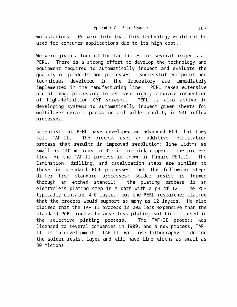
Scientists at PERL have developed an advanced PCB that they call TAF-II. The process uses an additive metalization process that results in improved resolution: line widths as small as 140 microns in 35-micron-thick copper. The process flow for the TAF-II process is shown in Figure PERL.1. The lamination, drilling, and catalyzation steps are similar to those in standard PCB processes, but the following steps differ from standard processes: Solder resist is formed through an etched stencil; the plating process is an electroless plating step in a bath with a pH of 12. The PCB typically contains 4-6 layers, but the PERL researcher claimed that the process would support as many as 12 layers. He also claimed that the TAF-II process is 20% less expensive than the standard PCB process because less plating solution is used in
162
Patricia M.H. Johnson, 01/03/-1,
Substitute “Solder resist is formed” for “Plating is selective” & delete sent. end. (Kanda)
Patricia M.H. Johnson, 01/03/-1,
Substitute 140 for 50 (Kanda)
Patricia M.H. Johnson, 01/03/-1,
Delete “based...(Takahashi)” (Kanda)
Geoff Holdridge, 01/03/-1,
Increase? (PMJ)
Patricia M.H. Johnson, 01/03/-1,
Substitute “bare” for “flip” (actually Kanda said “bear” — I think this was a spelling error)
Patricia M.H. Johnson, 01/03/-1,
Delete “5-year” ; also, “Current.....feasible.” sentence (Kanda)
Patricia M.H. Johnson, 01/03/-1,
Substitute “IC” for “camcorder” (Kanda)

Appendix C. Site Reports
the selective plating process. The TAF-II process was licensed to several companies in 1989, and a new process, TAF-III is in development. TAF-III will use lithography to define the solder resist layer and will have line widths as small as 80 microns.
Figure PERL.1. Brief process flow.
Dr. Makoto Iida presented work on thin molded plastics for laptop computer cases. He showed research on methods to reduce the thickness and mass of the plastic required for a domestic Japanese portable PC product, describing a roadmap for thinning body plastic thickness from 3 mm in 1985 to 1.5 mm in 1993. PERL researchers are currently working to reduce the size of the plastic case by improving structural design of the case, the polymer material used in the case, and mold design. Hitachi has developed its own polymeric material, together with an associated company. One of the greatest challenges is to control flow of the resin during filling of the mold. PERL researchers have analyzed resin flow using a simulation program to predict the best method to inject resin into thin molds. Dr. Iida stated that although composite materials can be made thinner, they are only used in higher-value products such as computer pen pads, due to the high cost of the material. Composite materials can be molded as thin as 1 mm and weigh less than conventional plastics. Overall thickness of the portable product was also reduced by using the LCD display as a structural
163
Patricia M.H. Johnson, 01/03/-1,
Change “developed a resin flow” to “analyzed a resin flow using a” (Kanda)
Patricia M.H. Johnson, 01/03/-1,
Substitute “solder resist” for “metal,” make layer singular, and change 20 to 80 (Kanda)

Appendix C. Site Reports
member. A shock-absorbing material was used to assure that LCD reliability remained high. Dr. Iida indicated that PERL is investigating molded circuit boards, but present cost of materials is very high. He indicated that the thermal expansion characteristics of the molded circuit board material are very important.
Dr. Iida then described a rework tool that has been developed to add or remove solder from SMT parts with a pitch as small as 0.3 mm. The tool removes excess solder using a braided wick, and adds solder using a novel technique. A droplet of solder is held by surface tension to the end of a heated point and the solder is placed on the unsoldered joint. The solder and the lead are heated in a single step.
There were several general comments made during the JTEC visit to Hitachi that are worthy of note. First, although a high level of automation is evident in the production philosophy of Hitachi, individuals at PERL emphasized the importance of an “appropriate” level of automation. They stressed that overdependence on automation is as detrimental as underdependence on automation. They further stressed the importance of the skilled individual to improve production yield and to retain production flexibility. The managers at PERL indicated that process floor workers should have a college education. When asked, they agreed that it is difficult to attract high-caliber people to production tasks, but indicated that showing employees the importance of their contribution to production is the best method to attract them.
A second theme was the importance of cost in all decisions regarding technology. Cost was clearly a critical consideration in every discussion regarding proposed technology. There was always a clear product path, and the cost of a technology was compared to a projected, required production cost. One statement made by Dr. Matsumura summarized this attitude. He said, “We used to determine the price of a product by adding an acceptable profit margin to the projected cost to produce a product. Now the price is a predetermined quantity, and we add an acceptable profit margin to arrive at the required product cost.”
164

Appendix C. Site Reports
Site: Ibiden Co., Ltd.3-200, Gama-Cho, Ogaki CityGifu Prefecture 503, Japan
Date Visited: October 5, 1993
Report Author: J. Peeples
ATTENDEES
JTEC:
M. KellyG. LimN. NaclerioJ. Peeples
HOSTS:
Mr. Hidetoshi Yamauchi Corporate Overseas Planning OfficeMr. Kazuhisa Ohno Manager of Sales and Marketing for the
Overseas Affairs DivisionMr. Osamu Fujikawa Director of Technology and DevelopmentMr. Koji Hosada General Manager of Overseas Marketing and
Sales of ElectronicsMr. Keiji Adachi Sales Engineer, Overseas Marketing and Sales
of Electronics
BACKGROUND
Ibiden began life as a power company and is now a manufacturer as well. It offers products in the following three areas:
IBI Electronics Branch
· double-sided/multilayer/special boards (small)· IC packaging based on the special board technology· continuous processing· up to 12 layers · width traces in the lab· small vias and blind/buried vias· flip chip on board (COB) for one customer· aluminum core substrates for power dissipationIBI Inorganic Chemical Branch
165

Appendix C. Site Reports
· calcium carbide/carbon/acetylene for the steel industry · fine-grain graphites - electrodes/fixtures· ceramic fibers - IBI, wool, insulator IBI Building Materials Branch
· IBI board - laminate material for home construction and decor· nonflammable construction materials
Ibiden shares its product branches between manufacturing plants. Any given plant may be involved in the production of electronics, building materials, inorganic chemicals, and/or new products. Generally, however, one or two plants specialize in production for a particular branch.
R & D ACTIVITIES IBI-Techno is the calling card of Ibiden's R&D activities. Advanced product development is conducted in the New Products Development Branch. When ready, the technology is fused into one of the major product branches. The development of plastic pin grid arrays (PGAs) and application-specific integrated modules (ASIMs) were discussed as examples of this advanced product development process. Ibiden discussed the ASIM concept with me during my April 1990 visit. I could not detect that the concept was any closer to product at the time of the JTEC visit in late 1993. Fundamental technology development is the charter of the Technology and Development Department. Activity in this area includes investigation of biotechnology, superconduction, ceramats, and optical materials.
Ibiden Electronics is working mainly in two product areas: IC packages and printed wiring boards (PWBs).
IC Package Products
Ibiden has leveraged its competency in laminate substrates technology into an IC package business. It makes small interposer substrates with facilities for chip attach (plated wirebond pads, semi-cavities, etc.) and add pins. Its major product line, by far, is the plastic pin grid array (PGA). It is very intense in this product development area, which is driving performance as well as costs. Our hosts showed examples of plastic PGA substrates in the 2 nH inductance range.
Ibiden has chosen to get out of the TAB package business because it feels that it was unable to compete with the major suppliers of TAB packages. It has just begun prototype production of BGA; it has one package of over 500 pins. Our hosts characterize this program as being very U.S.-centric but realize that some devices may have to be provided to U.S. end users by Japanese semiconductor vendors, and it therefore must do the package development.Substrate Products
166
Appendix C. Site Reports
Ibiden is a major supplier of PWBs. It produces subtractive laminate substrates at a rate of 25,000 square meters per month of double-sided substrates and 15,000 square meters per month of multilayer substrates. It is also active in several more advanced substrate areas, alternate materials for CTE and power dissipation, and additive processes for higher routing densities. Topan, which began life as a printing company, is a very important Ibiden competitor in laminate substrates. Yamamato and Compaq are also viewed as important competitors, especially for U.S. business. Samsung is a licensee of IBI-Techno.
Ceracom is a ceramic-cored PWB and is Ibiden's "low-cost," low-expansion substrate for flip chip. Ibiden currently single-sources Ceracom substrates but is interested in supplying the raw material and technology to U.S. substrate suppliers. It is not interested in supplying end products (substrates) of Ceracom to the United States. Ceracom currently has two major Japanese customers and few applications. Ceracom costs are between thin film metalized ceramic and FR-4 at the finished circuit board. Material cost is higher than ceramic substrate and FR-4.
Ibiden's additive process is still in the prototype stage of development. Development seems focused in the areas of adhesives, dry film plating resists, and plating technology. Plating technology is critical to the additive strategy. Ibiden is doing the work to ensure thickness consistency and peel strength. Thickness consistency is not a given, even in the electroless process. Peel strength is the major reliability concern. Ibiden's adhesive resin for additive process consists of two different epoxy resin systems (one is solid and the other is liquid). These resins show different strength against some chemicals by having different hardeners (e.g., acid and amine). This process additionally mitigates cracking in the high-stress regions of small vias. Peel strength is also a bit of a "specsmanship" issue in that strength levels have been characterized as appropriate to the older, much more macroscopic technologies, which may not extrapolate reasonably to the very-fine-pitch additive products. Ibiden is also investigating what can be done with solder resist height to make assembly of additive boards easier. Its researchers think that a product with a resist 20 mils higher than the copper trace can eliminate solder bridging.
Ibiden's build-up multilayer PWB product is still in development. Build-up is intended to be similar to IBM's surface laminar circuit (SLC). It is anticipated to be a double-sided subtractive core with two build-up fine-line layers on each side of the core (a total of six layers). Build-up will have a very high routing density due to the 50 µm conductor widths and the 100 µm vias. It is currently about five times the cost of a normal laminate substrate but about eight times less than an MCM-D substrate. Laminate substrates are the cost target for this technology.
The major changes in Ibiden's MCM-D substrate technology are the move away from polyimide to an epoxy dielectric for cost reduction and the deployment of a "hot press" aluminum nitride core for enhanced thermal conductivity and dimensional stability. This
167

Appendix C. Site Reports
extra stability results in a 1 mil line and 1 mil space capability for wiring. Ibiden feels that the $6-8 subtractive board of today would cost $40 in the MCM-L build-up technology, but sees a path to drive that to $15. The same circuitry would cost $300 today in a copper/polyimide MCM-D substrate or $120 for a copper/epoxy implementation.
GAMA PLANT TOUR
Mr. Fujikawa gave us a tour of the package production at the Gama plant. He feels that the current staffing level may be too high at about 300 persons, of which 20% are considered indirect. The plant was somewhat eclectic in layout and was literally covered in paper: SPC control charts with goal lines extended into 1995 were everywhere. There were safety and "one-point" displays in every section, as well. The "one-point" concept is an interesting one. A cache of visual aids is kept in each section from which the section supervisor or engineer can present a "one-point" discussion daily to the workers. The subject will be a very specific commentary on some facet of their job, like the correct way to use a tool or the details of why a particular process step is performed. There is no effort to tie the daily events together; the intent is rather to expose the workers daily to some level of very specific training.
The IC plastic package substrates and the Ceracom substrates are processed on very similar, if not the same, production lines. Drilling and routing of the package substrates takes place in a single room. Production control appears to be totally paper-based. There were paper travelers with every lot of material, and no bar code readers were seen to be integrated into any of the production steps. The design area was a large, well-lighted open office space that housed about 50 uniformed Ibiden and contract designers. Mr. Fujikawa again mentioned his concern that overhead support was duplicated within the various departments of the facility.
A major distinction between the package business at Ibiden and its substrate business is that the package business can focus on a relatively small customer set: the Gama plant deals with tens of customers, whereas the substrate plants must deal with five hundred to a thousand customers.
AOYANAGI PLANT TOUR
Ibiden manufactures laminate printed wiring boards at its Aoyanagi plant. It provides layout services for about 60% of its printed wiring board orders. This plant employs about 1,500 persons and exports about 30% of its production to Europe, the United States, and Singapore. This is the most active of all the IBI plants. It seemed busier, more disorganized, and a bit dirtier during this visit than it did during my visit in 1990. There were definitely more people in areas that were essentially fully automated during my last visit.
Work Environment
168

Appendix C. Site Reports
While safety awareness was apparent, there was no evidence of safety requirements. The smocking that did exist seemed much more focused on protection of the product (e.g., hats and masks to keep the product clean) than on human safety (e.g., lack of eyewear). The factory is by no means a "smoke-free environment." As in all Japanese factories, no street shoes are allowed.
GENERAL OBSERVATIONS AND CLOSING REMARKS
Below is a list of general observations and impressions:
· Primary electronic products are PWBs and IC packages.· Package products include COB, PGA, and plastic leadless chip carriers.· Product focus is on higher performance through higher density.· Ibiden is keeping R&D investment flat in spite of the Japanese economic slowdown.· R&D focus is on alternative materials and processes.· Ibiden provides product design service or can receive design data from its customers.· Ibiden provides low-volume or high-volume products and services.· Cost per product is volume-dependent.· Significant growth is expected in fine ceramics.· Ibiden designs and builds much of its own production equipment.· Environmental impact is a stated concern.· Some waste is managed on-site; some is transferred to specialty companies.· Economic slowdown resulted in excess capacity and underutilization.· While Ibiden does not expect to be fully utilized for some time, it is optimistic that it has
a bright future due to its investment in technology.
My summary impressions of Ibiden are very aligned with my overall impression of the visit to Japan. Having visited some of the same facilities and having met with some of the same people three years prior to this trip, I was very impressed with the company’s consistency of technology and product strategy. Ibiden seems to understand its core competency very well, although our hosts never spoke in those terms.
Ibiden Electronics does laminate PWB well. It is willing to drive that technology to new product opportunities (plastic PGAs), align it with other Ibiden technologies for new product opportunities (with ceramic for Ceracom), augment it for new product opportunities (with novel surface science for additive processes), and repeat the process (new ceramic cores and additive processes for the build-up MCM-D products).
I did sense a lack of visible progress. The laminate facility appeared very much as I had seen it three years earlier. Process control and worker communications technology seemed stagnant as well; however, neither of these seemed to limit the capability of the plants.
169

Appendix C. Site Reports
Site: Matsushita Electric Industrial Co., Ltd.3-1-1 Yagumo-Nakamachi, MoriguchiOsaka 570, Japan
Date Visited: October 6, 1993
Report Author: J. Peeples
ATTENDEES
JTEC:
M. KellyG. LimN. NaclerioJ. Peeples
HOSTS:
Keith Nishitani GM-Business Coordination, Overseas Dept. of theCorporate Technology Mgmt. Office
Dr. Yamazaki Director, Circuit Manufacturing Technology Lab., Corporate Production Engineering Division
Shunichi Murakami GM, Process and Materials Development Dept., Corporate Production Engineering Division
Mark Kawai GM, Control and SW Development Dept., Corporate Production Engineering Division
Hiroaki Fujimoto Senior Engineer, VLSI Technology Lab, Semiconductor Research Center
Yoshihiro Bessho Engineer for Materials and Components Research Lab, Components and Devices Research Center
Hiroshi Asai Manager, Marketing Department
BACKGROUND
Our visit was divided into three distinct sessions: a tour of the Circuit Manufacturing Technology Lab of the Corporate Production Engineering Division, a tour of a chip size inductor factory, and a discussion on chip mounting technology. The JTEC visit began right where my visit in 1990 had ended, in the Circuit Manufacturing Technology Lab, one of five subdivisions of the Corporate Production Engineering Division.
Mr. Murakami discussed the process development plans. Some of his handouts were identical to those I had been shown in 1990, only updated to show progress. Panasonic, like most of the Japanese companies I visited, seemed to have a remarkable degree of strategic technological consistency. My opinion is that similar U.S. companies are less likely to invest long-term in specific technologies, but would rather jump to new "promising" alternatives.
170

Appendix C. Site Reports
Mr. Hiroshi Asai, Manager of the Marketing Department, gave us a rough sketch of Matsushita:
· $60 billion company composed of 252,000 people· R&D budget of about $3 billion (5.8%) — flat for five years· 17 Japanese locations housing 30 organizations· 12 Divisions (including Panasonic FA)· 22 overseas manufacturing plants· component group revenue is $300 million/month from 80,000 product types
We were each presented a copy of My Management Philosophy by Matsushita's founder, Konosuke Matsushita. It is 66 pages full of gems of wisdom. Following are some of the quotables:
· Good times are good but bad times are still better.
· It is my hope that managers would use their knowledge as expert economists [to] work for measures that would be in the best interests of the people and the nation.
· Foreign expertise may still have a role to play but more important now is that Japan develop its own technologies.
· My proverb about management says that if we fight a hundred wars, we should win a hundred victories.
· You pray for the survival of your rival because you want another chance to demonstrate your superiority.
R&D ACTIVITIES
The Circuit Manufacturing Lab is the process and equipment development arm of Panasonic Factory Automation. It develops whatever is necessary to service new products. Much of the work in process is for palmcorder or for flat panel applications. We were told that about 20 engineers may be involved for three months to transfer a new FA line into production.
The lab we visited is set up for touring. A graphic arts display emphasized the importance of the Panasonic solder paste development to its fine-pitch (0.3 mm in production) stencil, place, and reflow process. The key point was that Panasonic has achieved a more spherical solder particle shape than normal, allowing the paste to have more predictable flow characteristics. Our hosts were excited about this and were similarly excited about their in-house-developed conductive epoxy; neither of these formulations are available for sale in the United States.
This lab exhibited the latest equipment technology for FA. New since my 1990 visit is the emphasis on lower-cost methods of direct chip attach and an increased involvement with
171

Appendix C. Site Reports
glass substrates. Panasonic is using normal wirebonders with a special shear cycle to attach a gold ball bond to an IC pad and immediately shear the wire at the top of the ball. This leaves a small tail (like a Hershey's Chocolate Kiss), which is then flip-mounted into conductive adhesive sites on a glass substrate. The process requires no tooling or wafer-level processing.
Another area that has developed dramatically since my last visit is the film area. Panasonic has put TAB into full use as a glass and PC board interconnection media. It has special equipment for what our hosts refer to as FOG (film on glass) and FOB (film on board). Both technologies are demonstrated as applied to flat panel display production. LCD drivers are mounted to a sliver of PC board material. A TAB interconnection is first hot bar bonded to the glass flat panel using anisotropically conductive adhesive tape. The other end of the TAB is then pulse laser bonded to the driver PC boards. With FOG and FOB, Panasonic has in place the first fully automated LCD assembly line in the world. The current line does a single edge of the LCD per cycle. The new generation will assemble all three edges simultaneously.
The Circuit Manufacturing Technology Lab, as a corporate staff function, provides assistance to all system divisions across the Matsushita group on SMT fine-pitch process and equipment development. It is primarily intended to enhance Matsushita Electric's manufacturing capability in order to increase its competitiveness. Membership is ¥600,000 annually, open only to Matsushita's system divisions, its subsidiary companies, and its affiliated companies, not to any party outside of Matsushita, regardless of whether it is a domestic or overseas entity.
Almost as an aside, we were given a tour of a factory of SMT mountable inductor coils. This facility was extremely noisy. Wireless headsets must be worn in order to hear the tour guide. Fine wire is automatically wound on a core that is terminated to a continuous leadframe and encapsulated. These are moved around on reels of 40,000 parts each. Parts are marked and visually inspected by computer, then excised from the lead frame and tested and binned. Velocity and quality are very high. Relatively large numbers of people are involved in this production.
Process improvements seem targeted at further integration of processes. The current process demands loading the test station from a parts feeder after excising from the continuous leadframe. After testing, parts are once again binned into parts feeders for final packaging. The new process will trim and test the parts and put them directly into rails to be packaged without the parts feeders. This new method reduces the space required for trimming, testing, and packaging by 10 square feet; floor space reduction was mentioned as a key reason for the improvement. As this station is replicated many times, this results in a significant utilization opportunity. One-fourth or more of the floor space appeared to be dedicated to test stations.Mr. Hiroaki Fujimoto, Senior Engineer of the VLSI Technology Research Lab, discussed transfer bump, micro bump, stud bump, and new bonding methods for chip assembly to substrates. Transfer bump is a method developed by Matsushita to displace the need for wafer scale processing to form the gold bumps required for TAB inner lead bonds. Gold bumps are formed on a glass substrate and transferred to the inner lead of the TAB frame via
172
Patricia M.H. Johnson, 01/03/-1,
Change 500,000 to 600,000 per Nishitani of Matsushita, letter dated 8/24/94

Appendix C. Site Reports
thermo-compression prior to inner lead assembly. Matsushita has marketed transfer bump worldwide for several years now.
Micro bump technology is a flip chip method that uses adhesive shrinkage to electrically and mechanically connect the interconnection bumps to a typically glass substrate. Micro bump uses glass and ceramic substrates. The adhesive is photo-curable; thus a more transparent substrate is naturally preferred, but edge-wise illumination will work with opaque substrates. Micro bump is currently in use in thermal print head assembly and is capable of 10 µm lead pitch.
Mr. Yoshihiro Bessho, Engineer for the Materials and Components Research Laboratory spoke on the stud bump bond (SBB) method of attachment. SBB employs the sheared gold ball bonds mentioned earlier to adhesively mount the chip to a variety of substrates. This technology is limited to pitches greater than 100 µm but is extremely flexible and simple in application. The ball bond studs are dipped into conductive adhesive and then glued to substrate. The wire bond "tails" are allowed to set the conductive paste penetration depth and apparently can do so accurately enough that bridging between bonds is not a problem. An undercoat adhesive more firmly secures the overall system.
Similar to what we saw and heard at Sony, Matsushita views process development on a par with product development. The Corporate Production Engineering Division (Circuit Manufacturing Technology Lab), reports at the highest level of the company and appears to be marketing what is considered a corporate core competency. As mentioned earlier, the consistent pursuit of a technological strategy is striking. The laboratory’s dedication to fine pitch or to transfer bump or other low-cost flip chip technologies is long-term and not likely to be redirected or curtailed short of the set objectives. The Matsushita strategy seems to be a familiar one: make it small and cheap!
173

Appendix C. Site Reports
Site: Matsushita-Kotobuki ElectronicsSaijo Division247 Fukutake, SaijoEhime, Japan
Date Visited: October 5, 1993
Report Author: R. Tummala
ATTENDEES
JTEC:
P. BarelaW. BoultonG. MeieranG. HarmanM. PechtR. Tummala
HOSTS:
Norio Meki Director, Research & Development LaboratoryHideo Sakai Assistant General Manager, Sales DepartmentHiroshi Yamauchi Manager, HIC Manufacturing SectionYasuyuki Baba Chief, Development Dept #5, R&D LaboratoryYasuhisa (John) Kobayashi Coordinator, Semiconductor and Appliance Section
BACKGROUND
Matsushita-Kotobuki Electronics Industries (MKE), Saijo Division, located in Saijo, Ehime Prefecture, on Shikoku Island, is one of the affiliated companies of the worldwide company Matsushita Electric Industries ($43.75 billion in FY 92), famous for the brand name "Panasonic." MKE, established in 1969, has several divisions in each prefecture on Shikoku and also subsidiaries in the United States, Singapore, Indonesia, and Ireland. Total 1992 sales were ¥308.9 billion (about $3 billion); annual investments were about ¥14 billion ($130 million).
MANAGEMENT, ORGANIZATION, AND PRODUCT CYCLES
The organization chart, Figure Pan.1, shows corporate functions including planning, personnel, general affairs, accounting, finance, administration, components purchasing and legal/patent section, and divisional arms that are independently managed. Each division is responsible for its own manufacturing, development, design, factory automation, and quality
174

Appendix C. Site Reports
assurance with corporate support from R&D Laboratory, Design Center and Quality Assurance Center.
Figure Pan.1. Organizational chart.
MKE has about 5,200 employees; the total number of engineers and personnel in manufacturing are 600 and 3,100, respectively.
The divisions work specifically to improve current technology for the products to be released within a couple of months while continuing to manufacture existing products. The corporate R&D Laboratory works to develop next-generation products together with the design section of each division. MKE creates new technology every two or three years that results in new products being introduced.
175

Appendix C. Site Reports
At the Saijo Division, 300,000-500,000 VCRs are manufactured per month. This high productivity is achieved by a high degree of factory automation.TECHNOLOGY
There are two packaging technologies in use at MKE, one using conventional PWB and the other using a ceramic substrate. MKE is perhaps one of very few companies using ceramic technologies in consumer products and pushing the leading-edge aspects of these technologies in achieving (1) miniaturization, (2) design standardization, (3) low cost, and (4) high reliability. MKE is using QFP with about 100 to 168 I/O at 0.5 mm lead pitch currently and is expected to migrate to 0.4 mm with forced air (N2) convection reflow.
The sophistication of MKE at Saijo is in ceramic technology based on hybrid IC (HIC) introduction in the late ‘70s and low-temperature co-fired ceramic (LTCC) technology used since 1990. MKE’s ceramic strategy during the last decade has been as follows:
Hybrid IC with Ag/Pd 1981Hybrid IC with Cu 1988LTCC with Cu 1990
The MKE plant had shipped about 60 million HICs and 170,000 LTCC modules as of the time of the JTEC visit. It has the capacity to manufacture about 1 million/month HICs and 10K/month LTCCs. Each handling size is roughly 4 inches square.
MKE’s LTCC technologies with Ag/Pd and copper are schematically illustrated in Figures 4.8 (p. 74) and 4.10 (p.75), respectively, showing the substrate characteristics that include the capacitors, resistors, and conductors. The current design ground rules being practiced are indicated in Figure Pan.2. Electrode pin allocation technology, such as lead frame, lead array, and BGA, is used for connecting LTCC and PWB. Pb(Mg1/3Nb2/3)O3-PbTiO3-PbO is the principal ingredient for embedded capacitors.
The LTCC is being used currently in peripheral application — tape memory systems — and is expected to be applied in cellular, automotive, camcorder, and computer applications. The LTCC has proven to be more advantageous than equivalent PWB process/materials relative to the application at system level.
MKE's LTCC process involves manufacturing the green sheet and producing approximately 0.10 to 0.15 mm diameter via holes on the green sheet by numerically- and mechanically-controlled punching equipment. After filling up and drying copper oxide paste into the via hole, conductor pattern is also applied on the green sheet by the copper oxide paste. These printed green sheets are laminated together under a heat pressure and fired at 550oC in air to remove organic components sufficiently. Then copper oxide is reduced to copper at 350oC in nitrogen atmosphere containing 10% hydrogen, and the copper and ceramic substrate are sintered at 900oC in nitrogen. This unique process provides highly reliable LTCC with copper electrode.
176
Patricia M.H. Johnson, 01/03/-1,
Request for formula change from Baba of MKE, letter dated 8/20/94

Appendix C. Site Reports
Figure Pan.2. Design rule (typical).
FUTURE TECHNOLOGY DIRECTIONS
Table Pan.1 shows the directions MKE is expected to take. The future directions include (1) upgrading LTCC by buried CR, (2) fine line by photo process, (3) BGA technology, (4) high-precision LTCC by nonshrinking process, and (5) flip chip.
Table Pan.1Future MKE Directions
Substrate Functions Future Technology Technology Elements
Substrate o Ag System Target
Internal Capacitor (Ag) 1994
o Cu System Non Shrinkage Substrate (Ag, Cu) 1994
Internal Resistor (Ag) ----
Photo Conductor L/S=50 / 50 mm (Cu) 1994
NI /Au plating (Cu) 1994
Bare Semiconductor o Wire Bonding Flip Chip (Ag, Cu) 1995
Device Attachment TAB ----
I/O Connection o Lead Frame
o Lead ArrayBGA 1994
177

Appendix C. Site Reports
Site: Meisei University2-590 Nagafuchi, Ome-shiTokyo 198, Japan
Date Visited: October 8, 1993
Report Author: W. R. Boulton
ATTENDEES
JTEC:
P. BarelaW.R. Boulton
HOSTS:
Dr. Otsuka
BACKGROUND
Dr. Otsuka recently retired from Hitachi to assume a position at Meisei University, where he teaches a course on advanced information technology. He is affiliated with IEEE and chaired the VLSI workshop held in Kyoto December 1994. He teaches computer and computer packaging technology. Through workshops, he teaches engineers from Japanese companies. He has research contracts on electrical characterization of packages.
PACKAGING TECHNOLOGY IN JAPAN
Dr. Otsuka limited his formal remarks to the topic of "Main Packaging Technology in Japan (Single Chip Packaging)." He provided a number of important insights into the future developments of electronic packaging technology in Japan.
Korea or America is expected to take over long-term leadership in LCD packaging technology.
Dr. Otsuka made it clear that LSI packaging technologies have a different origin and core competence than LCD packaging technologies. The development of LCD technologies has come from the merging of TV cathode tube and silicon wafer process technologies, which gives Koreans and Americans the potential to take leadership in this area. Korea has made a strong commitment to LCD development, and recently, Samsung and Gold Star have announced massive investments of $400 million and $300 million, respectively, in TFT technology development programs through 1995.
178
Geoff Holdridge, 01/03/-1,
Dr. Otsuka’s name should probably be here, and his first as well as last name, to be proper (PMJ)

Appendix C. Site Reports
Dr. Otsuka was not optimistic about Japanese companies maintaining leadership in CD technology. He didn't feel that large Japanese companies could work with small companies to develop such a new infrastructure. At the time, large companies were worried about small companies competing with them. Dr. Otsuka believed that Japanese companies' departmental structures were too competitive with each other to cooperate on merging new technologies. He felt that presidents cannot control their department heads. That means that they cannot develop large-scale systems like Apple did with Macintosh.
Small companies also provide a threat to large companies by their dedication to a single technology. While big companies are investing in CRT technology, they cannot give the same effort to new LCD technology. The large companies are worried about the potential of small companies. Active matrix LCDs by Japan Hosiden are a threat to Sharp because they are selling to Apple and other U.S. companies like Boeing. Companies like Sony are integrating backwards into their own components to increase profitability. That is causing a breakdown in supplier relationships and causing less coordination on new development.
In the future, Dr. Otsuka sees the United States maintaining strength in high-frequency devices like computers and microprocessors. He expects Korea will be strong in memories and LCDs in the future. Low-cost micro assembly applications will remain the strength of Japan in the future. If Japan loses low-cost QFP packaging technology, then he expects that Japan will be in trouble. Since plastic molded lead frame packages represent 85% of electronic product applications, Japan's electronic industry must continue to lead in this area.
Japan will remain the leader in LSI packaging technologies.
Dr. Otsuka said that over 85% of electronic packaging uses plastic molded lead frame technologies. Because these packaging technologies are so pervasive in Japanese industry and because so many companies are committed to them, he argues that Japan will continue to dominate in low-cost packaging technology. LSI packaging technologies include materials, parts, subassemblies, and assembly process. Most companies have specialized in specific areas of plastic packaging technology, which provides Japan with the strongest low-cost packaging infrastructure. This infrastructure is distributed across both large and small companies in Japan and, because it is pervasive, is unlikely to change its technological direction. He pointed out that it would be virtually impossible for any one company or group to change the technological focus of this infrastructure. Dr. Otsuka argued that, as a result, the low-cost electronic packaging industry in Japan will continue to develop current plastic packaging technology, because it is the easiest direction for all industry participants to continue in.
Low cost is top priority in the Japanese industry, which requires mass production technologies.
Because of Japan's cost requirements, Dr. Otsuka argued that LSI plastic packaging technology has to utilize mass production technology. This mass production orientation will continue to utilize existing packaging technologies. New technologies will require new mass
179
Geoff Holdridge, 01/03/-1,
LCD, perhaps? (PMJ)

Appendix C. Site Reports
production technologies, which would be expensive to develop and lead to higher costs. To keep from incurring such added costs, Dr. Otsuka argued that companies will continue to push existing packaging technologies to their limits rather than add new high-cost technologies. This strategy means that Japanese companies seek to solve performance problems related to current plastic packaging technologies.
Current plastic molded package technologies will meet future miniaturization requirements.
Dr. Otsuka feels that QFP packages can be designed with 0.15 mm pin pitch. Such fine pitch will allow 800 pins on a 32 mm package, or 1000 pins on a 40 mm package, or 384 pins on a 16 mm package. To support his argument, Dr. Otsuka gave examples of developments that are currently under production or development in Japan. He provided an example of 344 pins on a 28 mm package using 0.3 mm pin pitch that is currently in production at Hitachi.
Dr. Otsuka argued that Japan's strength is due to the extensive infrastructure of companies involved in plastic electronic packaging technology. Japanese companies have developed QFP packages with 500 pins, available from Nippon Printing Company by 1996, using 0.3 mm pin pitch. Some firms are currently developing this process using 0.2 mm pin pitch chips. This will allow plastic QFP packages to surpass ceramic PGA packages in pin density. Such strong development power comes from Japan's massive investment in all areas of plastic packaging technology. Nikkei Electronics described these developments in its August 2, 1993 issue (p. 94).
Dr. Otsuka also described Kyushu Matsushita's 0.15 mm pitch soldering process that he expects to be commercialized within several years. This process uses a solder precoat (super solder) with the body being pushed down as infrared heat is applied. The company uses solder bumps to ensure contact, but staggers the bumps to minimize shorting. This process would not require new machine technology for production utilization. Kyushu Matsushita is planning to use this approach in its next-generation camcorder production. While it is currently using TAB technology, Dr. Otsuka believes that the approach will be used with SMT in the future. Hitachi is currently producing circuits with 90 micron wire bonding on chips with spaces between the wire of 120 microns. Oki and Nippon Steel have demonstrated wire bonding with 40 micron pitch. Dr. Otsuka believes that we will see this in production in the future.
Fine pitch requires materials with higher resistivity. Fine pitch creates additional soldering problems by causing high current on the printed circuit board. Dr. Otsuka suggested that new materials will be used on fine-pitch boards. For example, conventional FR-4 through-hole resistivity is too low at 130°C to be used on fine-pitch boards. High Tg epoxy provides better resistivity, but for fine-pitch boards, the high resistivity requirements can be met with BT resin. Mitsubishi Gas Chemical has used BT resist (BTM 450) on contacts with 1.27 mm separation.
180

Appendix C. Site Reports
Japan will overcome low yield problems caused by fine pitch packages. Dr. Otsuka agreed that the move to fine pitch production will cause higher reject rates in the beginning. However, he argued that Japan has a long history of taking lower yield technology and improving it. In the United States, he believes that companies change technologies if they have low yields, but not in Japan. In addition, QFP is more inspectable than BGA even in low yield situations. Inspectability is very critical to ensuring quality products.
Finer pitch packages will automatically improve operating characteristics.
Fine pitch will increase product design flexibility. Since height is very important, single-layer boards are preferred in package design. Also, single boards are simpler to produce and are therefore cheaper to produce. Fine-pitch soldering would mean that we do not need two-layer bonding systems. Two-layer bonding has lower reliability because it depends on the solder connections. Simple packages are the best in every characteristic. For 0.3 mm pin pitch, a 40 mm2 QFP package can have over 500 pins. With 0.2 mm pin pitch, 34 mm2
packages can have 600 pins. At 0.15 mm pin pitch, we can have 600 pins on a 28 mm 2
package, comparable to a 1.0 mm pitch bump BGA chip. Dr. Otsuka used the previous examples to argue that these dense packages will be available within this decade.
Fine-pitch packages will provide additional advantages. Dr. Otsuka pointed out that finer pitch allows the use of three-set wiring design instead of two-set wiring between ground and power leads. Three-set wiring can increase output from 80-90 S to 95-105 S at 200 MHz and above. Finer pitch allows use of three-set packages for high-power packages. At the same time, impedance can be reduced once pin pitch falls below 0.3 mm. Japanese researchers have simulated 0.05 mm pin pitch designs and found that impedance drops 50%. Coupling capacitance can be further reduced in fine-pitch applications by using shorter wires. Shorter wires also means that multilayer wiring in single-chip packages is not essential. As long as power consumption stays below three watts per chip, chip scale packaging with short wires and fine-pitch provide the best design solutions. This has already been utilized in memory DRAM developments and should be viable in LSI packaging. As long as power consumption stays under 3 watts, natural cooling systems can be used and costs kept lower.
Dr. Otsuka also pointed out that reduced voltage requirements and reduced load capacitance can save power consumption (P=1/2*CV2). Lower voltage reduces coupling noise. He then argued that as we reduce package size, everything improves: "If we can communicate MHz at 3.3 volts, then the same package using 1.5 volts can operate at 400 MHz." He believes that QFP chip scale packages will be able to pass 200 MHz in the future.
QFP will be competitive with BGA on price-performance measures. Dr. Otsuka believes that QFP packages are better than BGA packages because they are inspectable and don't require new assembly technology. While the U.S. is interested in BGA because of its high pin count, Dr. Otsuka believes that 0.15 mm pin pitch on QFP packages will make them competitive with BGA alternatives. Since most Japanese companies do not have BGA capabilities, he expects continued QFP design and technology improvements to keep QFP packages cheaper than BGA packages.
181

Appendix C. Site Reports
Figure Meisei.1 shows the competitiveness of different packaging technologies, and additional insights offered by Dr. Otsuka are shown in Figure 4.5 (p. 64). Dr. Otsuka pointed out that ceramic substrates are cheaper in high-performance applications, but he believes that improvements described in the above statement will make QFP boards cost-competitive in future high-performance applications. The critical improvements are in the soldering process for wire bonding systems and in reducing popcorn problems of chips. If these problems can't be overcome, Japan will not be competitive in the future. But if Japanese firms can meet future miniaturization requirements with QFP technology, they will continue to be the low-cost producers of high-volume electronic packaging.
Figure Meisei.1. Competitiveness of different packaging technologies.
182

Appendix C. Site Reports
Dr. Otsuka believes single-chip packages will be cheaper than integrated chips on a substrate. He believes pushing the current technology to the limits will be cheaper than introducing new technology. Japan has alternative technologies, but low-cost plastic package technology is much cheaper. However, if package technology cannot achieve its improvement objectives, then its cost will cross over, and multichip technology will be cheaper.
Several technologies are unlikely to become dominant. Dr. Otsuka felt that adhesive conductors create too much noise and are too low in quality to replace solder connections. He continued to argue that the simple technology will survive. Reduction in size will reduce the problems of solder pollution and allow high-quality alternatives to be used. Because miniaturization will require less solder, it will be cost-effective.
Japanese companies guarantee everything about their products. Dr. Otsuka believes that they will continue to provide complete packages instead of bare chips. They want to control the assembly of their components to ensure their performance.
SUMMARY
Cost is the First Objective
There are three strategic objectives in Japanese competitive strategy. Since the mid-1980s the acronym "QCD" has been pervasive among Japanese companies: it stands for quality, cost, delivery.
All Japanese electronics suppliers are forced by their customers to keep lowering their costs. At the lowest cost, the company that provides the highest quality with the best availability or delivery wins sales. This puts great pressure on firms to reduce costs and improve quality as a daily activity. It also makes it extremely difficult for Japanese suppliers to make a high profit.
Miniaturization is Driving Automation
Sony has been driving consumer products technological development in Japan since the mid- 1980s when it introduced the minicamcorder. It has set the rules of the game for development by projecting that the next model be half the size and half the cost for the same function. For example, its first minicam was 1.6 kg, its second was 0.8 kg, and the most recent was 0.4 kg. The current technology driver is the cellular telephone at 0.2 kg. These small-sized products are pushing product components and packaging technologies to smaller sizes.
Continued commitment to the miniaturization of products and component technologies requires increased investment in production technologies and factory automation. As part sizes shrink, human assembly is no longer feasible. This has pushed assembly technologies to become more precise and faster. For example, precision robots have improved repeatability precision from 0.05 mm to 0.01 mm since the mid-1980s. Matsushita's new
183

Appendix C. Site Reports
SMT machine has 11 placement heads with 0.01 mm repeatability. Sony's high-speed robots are now working at 0.012 repeatability placement.
Miniaturization and Automation are Increasing Competitive Advantage
Japanese companies have been committed to miniaturization for nearly a decade. Product miniaturization is leading to improved product operating characteristics. Smaller component sizes lead to lower power usage and heat generation and longer battery life. Automation has led to improved quality and faster delivery of new products. Sony's factory automation activities have caused defect rates to drop to 20 ppm and have reduced ramp-up time to half that of manual assembly facilities. The goal of miniaturization has been supported by concurrent engineering in both product and process technology development. Companies have invested heavily in process technologies to achieve the miniaturization goals that can no longer be achieved through manual production techniques. By developing existing technologies rather than investing heavily in new technologies, they have been able to keep overall costs down and have stayed competitive in advanced consumer products.
High Technology is Only Used When Required
Japan's electronic packaging industry is heavily committed to plastic molded packaging systems. Cost as a competitive objective leads Japanese electronics suppliers to avoid high-technology solutions to their miniaturization problems. Current QFP packaging technologies are being pushed to their limits. Miniaturization of all components appears to be the strategy, not the movement to new technologies. New packaging technologies such as MCM are used when needed, but are considered higher-cost than established technologies. The miniaturization of current packaging technologies appears to be meeting the needs of most product requirements.
At the same time, high-technology packaging solutions are available in Japan in high-performance products such as supercomputers. A recent study of supercomputers found that Hitachi had the most advanced design for future MCM applications. This suggests that costs will limit the use of such technologies except where current technologies fail to meet the functional or size requirements of the package.
GROUP COMMENTS MADE DURING THE DISCUSSION AT NCR
· Japan is using simple, low-cost technologies to win the market.· Japan is committed to those simple technologies. · Concurrent engineering is required for simultaneous product and process developments.· Defense industries are driven by reliability and quality, and cause the cost to be high.
· Firms would be able to compete with Japanese firms if they were willing to make the investments. There are some production technologies that are not available in the United States. The equipment required for one micron of accuracy in miniaturized
184
Patricia M.H. Johnson, 01/03/-1,
I feel there should be more explanation of what this is

Appendix C. Site Reports
mechanical component production is probably outside of the U.S. capabilities today. We lack the required skills. Japan does not have the technology required to make advanced microprocessors.
· The U.S. believes that it can go to the moon if the commitment is made. It would require a number of years to rebuild the infrastructure and educate the people.
· The basic questions are, "What skills do we have? What do we want to do? What actions do we need to take to achieve those objectives?"
· All new products at the electronics show are smaller than the previous models. The only way that the U.S. will compete is to get into the market.
· The U.S. dominates the market in design tools and microprocessors. This should provide some opportunity for development. U.S. firms have designed but not exploited technologies.
· Most firms produce their own equipment and plan to build even more of their equipment in the future. The ability to produce is a constraint to getting into the business. Some firms have developed their own equipment to sell their components. They use other makers’ equipment, but build their own when equipment is not available to meet their own needs. So why is TI selling off its equipment business?
· The companies we visited build a high portion of their own equipment and place a high priority on production technology.
· Most firms said they were not going to get into BGAs, but would push today's technology to the limit. Those firms going to TAB may be taking a high-cost alternative.
185
Patricia M.H. Johnson, 01/03/-1,
This seems to make more sense to me in the negative, but “not” is my addition, not the author’s

Appendix C. Site Reports
Site: Murata Manufacturing Co., Ltd.2-26-10 Tenjin, Magaokakyo-shiKyoto 617, Japan
Date Visited: October 6, 1993
Report Author: M. Kelly
ATTENDEES
JTEC:
M. KellyG. LimN. NaclerioJ. Peeples
HOSTS:
H. Kuronaka Manager, R&D Management SectionH. Iwatsubo Assistant Chief, R&D Section
BACKGROUND
Murata is a leader in the production of discrete electronic components. The primary market for Murata products is Japan (63%), followed by the United States (11%), Europe (10%), and Asia (most of the remaining 16%). The company strategy is to pursue manufacturing within the geographical spheres of its primary customers. The Murata group includes 23,000 employees and 47 affiliates, including 23 overseas; Murata Erie North America, for example, has two plants in Georgia, one of which makes capacitors and the other of which makes passive electronic components. Based on information contained in the 1993 annual report, the primary product groups in Murata are the following:
· Capacitors. This group produces monolithic disk-type and semiconductor ceramic and trimmer capacitors.
· Resistors. This group produces PTC thermistors, potentiometers, R-networks and high- voltage resistors. Demand comes primarily from Japanese display manufacturers.
· Piezoelectrics. This group produces ceramic filters, ceramic resonators, piezoelectric buzzers, and surface acoustic wave filters.
· Coils. This group produces flyback transformers, deflection yokes, and various types of coils. The major expansion was in sales of high-definition and microwave deflection yokes for computer displays in the Japanese and Asian markets.
186

Appendix C. Site Reports
· Electronic Modules. This group produces circuit modules and power supplies. There has been a high demand in overseas markets for voltage controlled oscillators for mobile and portable telephones.
· Other Products. There is a wide variety of “other products” that include EMI suppression filters, microwave filters, sensors, piezoelectric vibrating gyroscopes, thermal cutoffs, and production equipment. The most attractive markets are in the areas of EMI suppression filters for computers, piezoelectric vibrating gyroscopes for camcorders, and in the future, compact switching regulators (2 MHz) for notebook PCs.
Murata sales total about $2.7 billion annually, with capacitors representing 38% and piezoelectric components 20%. We were told that Murata dominates world market share of ceramic filters/ceramic resonators (85%, $100 million/mo), capacitors (50%), thermistors (40%), and EMI suppressors (30%).
Murata’s product strategy is to continue to build on its strengths and move aggressively to be a supplier of complete functional modules. In pursuit of future objectives, Murata is spending 6.5% of sales, about $176 million, on R&D.
Murata’s primary R&D domains include
· microwave modules (for digital cordless telephones): oscillators, mixers, synthesizers, antennas, filters, GaAs MMICs
· power supplies (SW frequency 2 MHz): CAD, substrates, packaging, transformers, capacitors
· functional sensor modules: gyro sensors, IR sensor arrays, signal processing, technology integration
· capacitors (miniature, high capacitance): thin film multilayer, ceramic, reliability, electrode materials
· filters (for communications): piezoelectric ceramic products, high-Q ceramics, thin-film process
Murata’s strategic technologies are identified in Figure 7.5 (p. 137). Other areas considered important by Murata include module circuit application-specific components and vertical technology integration within the company.
As of the JTEC visit, recent capital investments had been made for the production of ceramic materials, monolithic ceramic capacitors, components for imaging equipment, chip components, microwave components, and electronic modules. Aggressive capital investments were also made for thin-film processing technology and the development of equipment for gallium-arsenide semiconductor devices.
187

Appendix C. Site Reports
At the time of the JTEC visit, Murata planned to have a gallium-arsenide integrated circuit pilot line in production by the end of 1994. The motivation for establishing the line, as expressed by our hosts, is to protect intellectual property and to improve Murata’s competitive posture in the microwave and RF module business by focusing on future personal communication products.
Murata is doing extensive work in sensor development. Present applications for sensor products include engine knock detectors and fire and burglar alarms. An advanced sensor application that was discussed is a piezoelectric gyro for sensing angular accelerations. The current product measures 21.5 x 8 x 8.5 mm and is used in the Sony TR2 and TR3 palm-sized camcorder for vibration stabilization. A larger, more accurate version (24 x 24 x 58 mm) is used in Pioneer’s automobile GPS navigation systems. Future markets for Murata sensors include accelerometers and chemical/gas detection.
A new silicon micromachining program has been initiated at the Yokohama R&D Center to develop microminiature accelerometers, sensors, and oscillators.
The manufacturing lines JTEC panelists toured in Kyoto are most impressive. The total process is automated. The equipment appears to be very robust and capable of handling very high-volume throughput. Over 80% of the equipment being used was designed and built by Murata. Much of the equipment is customized to meet specific product requirements, which justifies the in-house development; however in more general terms, Murata recognizes the importance of internal equipment development in order to protect its competitive advantages. There was evidence of continuous improvement in the manufacturing processes, with particular emphasis on equipment improvements.
Murata has evidently mastered the manufacturing process for high-volume, miniaturized discrete components. Perhaps this explains its dominance in the world market. There was nothing magic about what we saw: outstanding equipment designed for automation, meticulous attention to detail, continuous improvement, qualified personnel, and a committed management team.
It became very evident during our discussions that Murata places a very high priority on customer interactions. It was pointed out that in some cases Murata people visit customers once or twice a day. Procurement planning is regularly updated, and Murata can expect at least a three-year lead time from customers for new product requirements. It was likewise evident that the needs of suppliers were taken into account when negotiating reduced costs. Suppliers, it was stated, are no good to us if they are driven into bankruptcy. Suppliers are considered part of the team and expected to contribute to the competitiveness of the product.
The visit to Murata substantiated much of what has been identified as Japanese strengths:
· Focus on the fundamentals· Pursue continuous improvements· Drive continuously to miniaturize components
188

Appendix C. Site Reports
· Work closely with suppliers and customers· Design and build your own equipment· Eliminate waste· Make cost reduction a primary objective in design and manufacturing· Automate whenever it is cost-justified· Build on core competencies· Follow an evolutionary product strategy· Move increasingly to integrate components to produce functional modules
Murata, like other Japanese companies visited, was concerned about the effects of the recessionary period that industry was experiencing at the time of the JTEC visit. The attitude of our hosts, however, was very positive about the future of Murata. If anything, I expect that the present economic climate will strengthen the company and better prepare it for the competitive challenges of the future.
189