APOC 2007 Best Student Paper Awards BRIEFS … · · 2012-07-19The Best Student Paper Awards were...
8
REVIEW JANUARY-JUNE 2008 RSOFT DESIGN GROUP VOLUME 7 NUMBER 1 Modeling Light Scattering from Biological Cells and Cell-Clusters using Fullwave. Electronic dispersion compensation (EDC) has recieved particular attention lately for its potential to correct for signal distortion in optical communication systems in the electrical domain after photo-detection, thereby promoting system cost savings and new network configurations with fewer regenera- tion sites. Types of linear and nonlinear distortion addressed by EDC include chromatic dispersion, polarization mode dispersion (PMD), modal dispersion and self-phase modulation (SPM). The maximum likelihood sequence estimation (MLSE) represents a particularly promising version of EDC. In particular, this nonlin- ear equalization technique has performance advantages for the correction of chromatic dispersion distortions over other algorithms such as feed-forward equalization (FFE) and decision-feedback equalization (DFE). Recent simulation and experimental results have shown MLSE-based receivers to be capable of supporting uncompensated transmission over standard single-mode fiber exceeding 1,000 Km at 10 Gbit/s for a total accumulated disper- sion of over 17,000 ps/nm. In comparison FFE- and DFE- based receivers have been shown to be limited to dispersion values between 2,000 and 4,000 ps/nm. OptSim™ includes a new advanced block implementing an efficient MLSE processor to be used in intensity-modulation direct-detection (IMDD) optical receivers. The model consists of an analog-to-digital (A/D) converter where samples are sent to a parallel bank of branch metric computation stages. The extracted metric is sent to a Viterbi processor, which uses a reduced-state algorithm. The resolution of 1 Spectral and angular properties of light scattered from biological tissue have been demonstrated to provide important diagnostic information of tissue and cellular structures on the micro and nano scales, with applications including but not limited to confocal and optical coherence tomography, light-scattering spectroscopy, spec- tral imaging, and flow cytometry. Moreover, it has been recently shown that observing the spectrum of back-reflected light from biological cell-clusters yields much more information regarding pre-cancerous conditions than any other minimally invasive optical technology. These advancements in optical tissue diagnostic technology have necessitated the need for rigorous simulation techniques capable of hand- ling such complex structures as the biological tissue. Traditional simulation techniques that are used to study tissue optics treat tissue and cellular structures as homogeneous spheres. These methods are unable to rigorously handle inhomogeneities in the cell morphology and structure, which have been shown to considerably effect the scattering properties. Moreover, these techniques generally neglect the full-vector electromagnetic Maximum Likelihood Sequence Estimation (MLSE) Receiver for Uncompensated Transmission System Simulation in OptSim. continued on page 2 continued on page 2 FIGURE 1: OptSim project layout of a direct- detection system with uncompen- sated transmission at 10 Gbit/s over 700 Km G.652 fiber deploying a 8192 state MLSE Viterbi processor at the receiver. The eye diagram appears to be completely closed. 1.0 1.2 Contour Map of Index Profile at Y=0 X (μm) Z (μm) 5 - 3 - 1 - 1 3 5 0 2 4 6 8 Scattering Angle (deg) 0 20 40 60 80 100 120 140 160 180 log(DSCS) 13 - 12 - 11 - 10 - 9 - 8 - 7 - Mie FullWAVE FIGURE 1: FullWAVE computed differential scattering cross-section (DSCS) as a function of angle validated against the analytic solution from Mie theory. The simulation parameters were as follows: diameter=8μm, index=1.2, λ=0.75μm.
Transcript of APOC 2007 Best Student Paper Awards BRIEFS … · · 2012-07-19The Best Student Paper Awards were...
For the fourth straight year, RSoft sponsored the Best Student PaperAwards at APOC November 1-5, 2007 at the Wuhan Science and Technology Convention and Exhi-bition Center in Wuhan, China. The Best Student Paper Awards were created to encourage participation and involvement of young engineers and scientists.
Also at APOC, our technical team submitted an invited paper, PhysicalLayer Modeling of Passive Optical Networks. RSoft authors include Jigesh Patel, Dwight Richards, Enrico Ghillino, Pablo Mena, Anil Panicker and Zhengyu Huang. The paper is available by contacting RSoft Design Group at [email protected]. The winning papers were:
Simulation and analysis of fiber Bragg grating-based Q-switched fiber laser with sidelobes’ influence consideration, by X. P. Cheng, Nanyang Technological Univ. (Singapore)
1.55 µm extremely efficient and polarization insensitive tunable Mach-Zehnder wavelength duplexer based on an InGaAsP/InP ridge waveguide structure, by L. Xu, Technische Univ. Eindhoven (Netherlands)
SBS based slow-light performance comparison of 10-Gb/s NRZ, PSBT and DPSK signals, by Lilin Yi, GET/Telecom Paris and Shanghai Jiao Tong Univ. (China)
A novel protection scheme for a hybrid WDM/TDM PON, by Jiajia Chen, RoyalInstitute of Technology KTH (Sweden) and Zhejiang Univ. (China).
Greg D. MillerCollinear CorporationUSA
Pu DonglinSuzhou UniversityChina
Lucia MarazziCoreComItaly
RSoft Co-sponsors Workshop on Optical Fibre Sensors and Components.
RSoft proudly co-sponsored the Workshop on Optical Fibre Sensors and Components, jointly organized by the British High Commission and the Indian Institute of Technology (IIT), Delhi at the British Council Auditorium in New Delhi, India. The three-day (December 7-9, 2006) work-shop brought together recognized international experts from the UK and their colleagues from India. The workshop provided a common platform to encourage Indo-British research and development co-operation in fibre optic sensors and guided wave opticalcomponent technologies. RSoft, being a global leader in providing photonic modeling tools for these technologies, always strives to help emerging econo-mies culminate their research from its nascency into an eventual industrial manufacturing phase.
APOC 2007 Best Student Paper AwardsSponsored by RSoft Design Group
REVIEWJANUARY-JUNE 2008 RSOFT DESIGN GROUP
VOLUME 7NUMBER 1
Modeling Light Scattering from Biological Cells and Cell-Clusters using Fullwave.
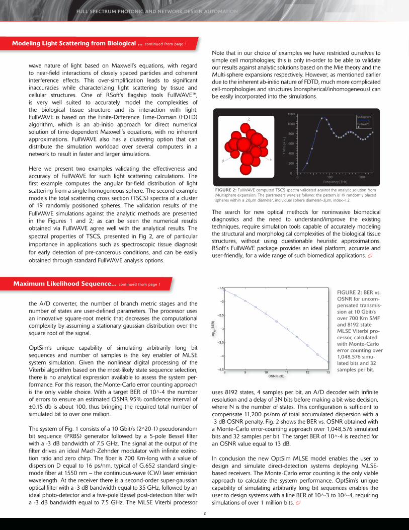
Electronic dispersion compensation (EDC) has recieved particular attention lately for its potential to correct for signal distortion in optical communication systems in the electrical domain after photo-detection, thereby promoting system cost savings and new network configurations with fewer regenera-tion sites. Types of linear and nonlinear distortion addressed by EDC include chromatic dispersion, polarization mode dispersion (PMD), modal dispersion and self-phase modulation (SPM).
The maximum likelihood sequence estimation (MLSE) represents a particularly promising version of EDC. In particular, this nonlin-ear equalization technique has performance advantages for the correction of chromatic dispersion distortions over other algorithms such as feed-forward equalization (FFE) and decision-feedback equalization (DFE). Recent simulation and experimental results have shown MLSE-based receivers to be capable of supporting uncompensated transmission over standard single-mode fiber exceeding 1,000 Km at 10 Gbit/s for a total accumulated disper-sion of over 17,000 ps/nm. In comparison FFE- and DFE- based receivers have been shown to be limited to dispersion values between 2,000 and 4,000 ps/nm.
OptSim™ includes a new advanced block implementing an efficient MLSE processor to be used in intensity-modulation direct-detection (IMDD) optical receivers. The model consists of an analog-to-digital (A/D) converter where samples are sent to a parallel bank of branch metric computation stages. The extracted metric is sent to a Viterbi processor, which uses a reduced-state algorithm. The resolution of
1
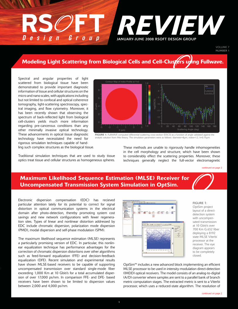
Spectral and angular properties of light scattered from biological tissue have been demonstrated to provide important diagnostic information of tissue and cellular structures on the micro and nano scales, with applications including but not limited to confocal and optical coherence tomography, light-scattering spectroscopy, spec-tral imaging, and flow cytometry. Moreover, it has been recently shown that observing the spectrum of back-reflected light from biological cell-clusters yields much more information regarding pre-cancerous conditions than any other minimally invasive optical technology. These advancements in optical tissue diagnostic technology have necessitated the need for rigorous simulation techniques capable of hand- ling such complex structures as the biological tissue.
Traditional simulation techniques that are used to study tissue optics treat tissue and cellular structures as homogeneous spheres.
These methods are unable to rigorously handle inhomogeneities in the cell morphology and structure, which have been shown to considerably effect the scattering properties. Moreover, these techniques generally neglect the full-vector electromagnetic
Maximum Likelihood Sequence Estimation (MLSE) Receiver for Uncompensated Transmission System Simulation in OptSim.
continued on page 2
continued on page 2
BRIEFS
8
FOE Tokyo Big Sight, Japan 16-18 January TBA*
Photonics WEST San Jose, California 22-24 January 907
Nano tech Tokyo Big Sight, Japan 13-15 February TBA*
OFC/OFOEC San Diego, California 26-28 February 1926
PV EXPO Tokyo Big Sight, Japan 27-29 February TBA*
Defense + Security Orlando, Florida 18-20 March 2016
Photonics Europe Strasbourg, France 8-10 April 320
Laser EXPO Tokyo Big Sight, Japan 23-25 April TBA*
CLEO San Jose, California 6-8 May 2216
ECIO Eindhoven, The Netherlands 11-13 June TBA*
UNITED STATES Corporate headquarters
Rsoft Design Group, Inc.400 Executive Boulevard, Ste. 100Ossining, NY 10562, USA
PHONE: 914.923.2164 E-MAIL: [email protected] WEB: www.rsoftdesign.com
JAPANRsoft Design Group Japan KKMatsura Building 2F, 1-9-6 Shiba Minato-ku, Tokyo, 105-0014 Japan
PHONE: + 81.3.5484.6670 EMAIL: [email protected]
EUROPERSoft Design UK, Ltd.11 Swinborne DriveSpringwood Industrial EstateBraintree, Essex CM7 2YP
PHONE: 44 (0)1376 528556 EMAIL: [email protected]
Visit us at the following tradeshows – 2008 FIRST HALF
SHOW LOCATION DATE BOOTH #
– 2008 FIRST HALF
FIGURE 1: OptSim project layout of a direct-detection system with uncompen-sated transmission at 10 Gbit/s over 700 Km G.652 fiber deploying a 8192 state MLSE Viterbi processor at the receiver. The eye diagram appears to be completely closed.
Frequency [THz]0 100 200
TSC
S [a
.u.]
0
200
400
600
800
1000
1200Multisphere
FullWAVE
1.0
1.2Contour Map of Index Profile at Y=0
X (μm)
Z (μ
m)
5- 3- 1- 1 3 5
0
2
4
6
8
Scattering Angle (deg)0 20 40 60 80 100 120 140 160 180
log(
DSC
S)
13-
12-
11-
10-
9-
8-
7-Mie
FullWAVE
FIGURE 1: FullWAVE computed differential scattering cross-section (DSCS) as a function of angle validated against the analytic solution from Mie theory. The simulation parameters were as follows: diameter=8µm, index=1.2, λ=0.75µm.
FIGURE 2: FullWAVE computed TSCS spectra validated against the analytic solution fromMultisphere expansion. The parameters were as follows: the pattern is 19 randomly placed spheres within a 20µm diameter, individual sphere diameter=3µm, index=1.2.
iPod Winners from the Survey!
*Please check our website for the latest tradeshow information.
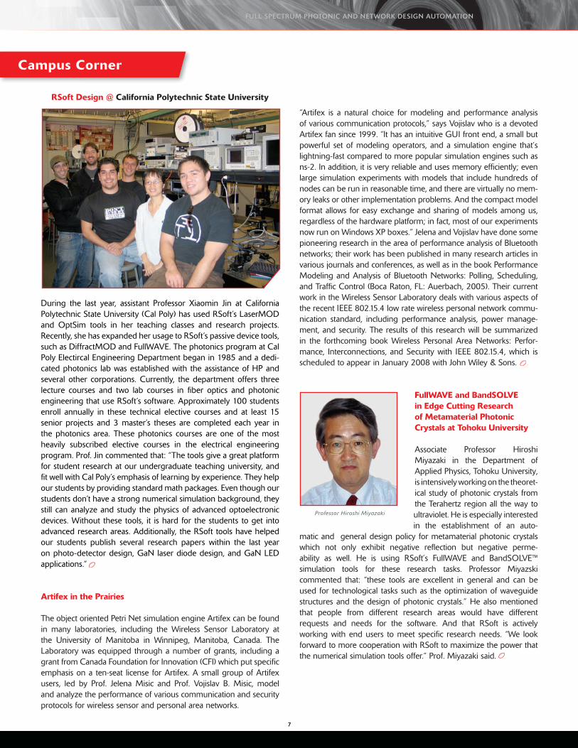
RSoft Design @ California Polytechnic State University
During the last year, assistant Professor Xiaomin Jin at California Polytechnic State University (Cal Poly) has used RSoft’s LaserMOD and OptSim tools in her teaching classes and research projects. Recently, she has expanded her usage to RSoft’s passive device tools, such as DiffractMOD and FullWAVE. The photonics program at Cal Poly Electircal Engineering Department began in 1985 and a dedi-cated photonics lab was established with the assistance of HP and several other corporations. Currently, the department offers three lecture courses and two lab courses in fiber optics and photonic engineering that use RSoft’s software. Approximately 100 students enroll annually in these technical elective courses and at least 15 senior projects and 3 master’s theses are completed each year in the photonics area. These photonics courses are one of the most heavily subscribed elective courses in the electrical engineering program. Prof. Jin commented that: “The tools give a great platform for student research at our undergraduate teaching university, and fit well with Cal Poly’s emphasis of learning by experience. They help our students by providing standard math packages. Even though our students don’t have a strong numerical simulation background, they still can analyze and study the physics of advanced optoelectronic devices. Without these tools, it is hard for the students to get into advanced research areas. Additionally, the RSoft tools have helped our students publish several research papers within the last year on photo-detector design, GaN laser diode design, and GaN LED applications.“
Artifex in the Prairies
The object oriented Petri Net simulation engine Artifex can be found in many laboratories, including the Wireless Sensor Laboratory at the University of Manitoba in Winnipeg, Manitoba, Canada. The Laboratory was equipped through a number of grants, including a grant from Canada Foundation for Innovation (CFI) which put specific emphasis on a ten-seat license for Artifex. A small group of Artifex users, led by Prof. Jelena Misic and Prof. Vojislav B. Misic, model and analyze the performance of various communication and security protocols for wireless sensor and personal area networks.
“Artifex is a natural choice for modeling and performance analysis of various communication protocols,” says Vojislav who is a devoted Artifex fan since 1999. “It has an intuitive GUI front end, a small but powerful set of modeling operators, and a simulation engine that’s lightning-fast compared to more popular simulation engines such as ns-2. In addition, it is very reliable and uses memory efficiently; even large simulation experiments with models that include hundreds of nodes can be run in reasonable time, and there are virtually no mem-ory leaks or other implementation problems. And the compact model format allows for easy exchange and sharing of models among us, regardless of the hardware platform; in fact, most of our experiments now run on Windows XP boxes.” Jelena and Vojislav have done some pioneering research in the area of performance analysis of Bluetooth networks; their work has been published in many research articles in various journals and conferences, as well as in the book Performance Modeling and Analysis of Bluetooth Networks: Polling, Scheduling, and Traffic Control (Boca Raton, FL: Auerbach, 2005). Their current work in the Wireless Sensor Laboratory deals with various aspects of the recent IEEE 802.15.4 low rate wireless personal network commu-nication standard, including performance analysis, power manage-ment, and security. The results of this research will be summarized in the forthcoming book Wireless Personal Area Networks: Perfor-mance, Interconnections, and Security with IEEE 802.15.4, which is scheduled to appear in January 2008 with John Wiley & Sons.
FullWAVE and BandSOLVE in Edge Cutting Research of Metamaterial Photonic Crystals at Tohoku University
Associate Professor Hiroshi Miyazaki in the Department of Applied Physics, Tohoku University, is intensively working on the theoret-ical study of photonic crystals from the Terahertz region all the way to ultraviolet. He is especially interested in the establishment of an auto-
matic and general design policy for metamaterial photonic crystals which not only exhibit negative reflection but negative perme-ability as well. He is using RSoft’s FullWAVE and BandSOLVE™ simulation tools for these research tasks. Professor Miyazski commented that: “these tools are excellent in general and can be used for technological tasks such as the optimization of waveguide structures and the design of photonic crystals.” He also mentioned that people from different research areas would have different requests and needs for the software. And that RSoft is actively working with end users to meet specific research needs. “We look forward to more cooperation with RSoft to maximize the power that the numerical simulation tools offer.” Prof. Miyazaki said.
2 7
the A/D converter, the number of branch metric stages and the number of states are user-defined parameters. The processor uses an innovative square-root metric that decreases the computational complexity by assuming a stationary gaussian distribution over the square root of the signal.
OptSim’s unique capability of simulating arbitrarily long bit sequences and number of samples is the key enabler of MLSE system simulation. Given the nonlinear digital processing of the Viterbi algorithm based on the most-likely state sequence selection, there is no analytical expression available to assess the system per-formance. For this reason, the Monte-Carlo error counting approach is the only viable choice. With a target BER of 10^-4 the number of errors to ensure an estimated OSNR 95% confidence interval of ±0.15 db is about 100, thus bringing the required total number of simulated bit to over one million.
The system of Fig. 1 consists of a 10 Gbit/s (2^20-1) pseudorandom bit sequence (PRBS) generator followed by a 5-pole Bessel filter with a -3 dB bandwidth of 7.5 GHz. The signal at the output of the filter drives an ideal Mach-Zehnder modulator with infinite extinc-tion ratio and zero chirp. The fiber is 700 Km-long with a value of dispersion D equal to 16 ps/nm, typical of G.652 standard single-mode fiber at 1550 nm – the continuous-wave (CW) laser emission wavelength. At the receiver there is a second-order super-gaussian optical filter with a -3 dB bandwidth equal to 35 GHz, followed by an ideal photo-detector and a five-pole Bessel post-detection filter with a -3 dB bandwidth equal to 7.5 GHz. The MLSE Viterbi processor
uses 8192 states, 4 samples per bit, an A/D decoder with infinite resolution and a delay of 3N bits before making a bit-wise decision, where N is the number of states. This configuration is sufficient to compensate 11,200 ps/nm of total accumulated dispersion with a -3 dB OSNR penalty. Fig. 2 shows the BER vs. OSNR obtained with a Monte-Carlo error-counting approach over 1,048,576 simulated bits and 32 samples per bit. The target BER of 10^-4 is reached for an OSNR value equal to 13 dB.
In conclusion the new OptSim MLSE model enables the user to design and simulate direct-detection systems deploying MLSE-based receivers. The Monte-Carlo error counting is the only viable approach to calculate the system performance. OptSim’s unique capability of simulating arbitrarily long bit sequences enables the user to design systems with a line BER of 10^-3 to 10^-4, requiring simulations of over 1 million bits.
wave nature of light based on Maxwell’s equations, with regard to near-field interactions of closely spaced particles and coherent interference effects. This over-simplification leads to significant inaccuracies while characterizing light scattering by tissue and cellular structures. One of RSoft’s flagship tools FullWAVE™, is very well suited to accurately model the complexities of the biological tissue structure and its interaction with light. FullWAVE is based on the Finite-Difference Time-Domain (FDTD) algorithm, which is an ab-initio approach for direct numerical solution of time-dependent Maxwell’s equations, with no inherent approximations. FullWAVE also has a clustering option that can distribute the simulation workload over several computers in a network to result in faster and larger simulations.
Here we present two examples validating the effectiveness and accuracy of FullWAVE for such light scattering calculations. The first example computes the angular far-field distribution of light scattering from a single homogeneous sphere. The second example models the total scattering cross section (TSCS) spectra of a cluster of 19 randomly positioned spheres. The validation results of the FullWAVE simulations against the analytic methods are presented in the Figures 1 and 2; as can be seen the numerical results obtained via FullWAVE agree well with the analytical results. The spectral properties of TSCS, presented in Fig 2, are of particular importance in applications such as spectroscopic tissue diagnosis for early detection of pre-cancerous conditions, and can be easily obtained through standard FullWAVE analysis options.
Note that in our choice of examples we have restricted ourselves to simple cell morphologies; this is only in-order to be able to validate our results against analytic solutions based on the Mie theory and the Multi-sphere expansions respectively. However, as mentioned earlier due to the inherent ab-initio nature of FDTD, much more complicated cell-morphologies and structures (nonspherical/inhomogeneous) can be easily incorporated into the simulations.
The search for new optical methods for noninvasive biomedical diagnostics and the need to understand/improve the existing techniques, require simulation tools capable of accurately modeling the structural and morphological complexities of the biological tissue structures, without using questionable heuristic approximations. RSoft’s FullWAVE package provides an ideal platform, accurate and user-friendly, for a wide range of such biomedical applications.
Modeling Light Scattering from Biological ... continued from page 1
Maximum Likelihood Sequence... continued from page 1
Campus Corner
FULL SPECTRUM PHOTONIC AND NETWORK DESIGN AUTOMATION FULL SPECTRUM PHOTONIC AND NETWORK DESIGN AUTOMATION
Frequency [THz]0 100 200
TSC
S [a
.u.]
0
200
400
600
800
1000
1200Multisphere
FullWAVE
1.0
1.2Contour Map of Index Profile at Y=0
X (μm)
Z (μ
m)
5- 3- 1- 1 3 5
0
2
4
6
8
Scattering Angle (deg)0 20 40 60 80 100 120 140 160 180
log(
DSC
S)
13-
12-
11-
10-
9-
8-
7-Mie
FullWAVE
FIGURE 1: FullWAVE computed differential scattering cross-section (DSCS) as a function of angle validated against the analytic solution from Mie theory. The simulation parameters were as follows: diameter=8µm, index=1.2, λ=0.75µm.
FIGURE 2: FullWAVE computed TSCS spectra validated against the analytic solution fromMultisphere expansion. The parameters were as follows: the pattern is 19 randomly placed spheres within a 20µm diameter, individual sphere diameter=3µm, index=1.2.
8 9 10 11 12 13−4.5
−4
−3.5
−3
−2.5
−2
−1.5
OSNR [dB]
log 10
(BER
)
FIGURE 2: BER vs. OSNR for uncom-pensated transmis-sion at 10 Gbit/s over 700 Km SMF and 8192 state MLSE Viterbi pro-cessor, calculated with Monte-Carlo error counting over 1,048,576 simu-lated bits and 32 samples per bit.
Professor Hiroshi Miyazaki
to differentiate different types of traffic. The MAC protocol at the node object is subdivided into Access Strategy, Fairness Control and Reser-vation Strategy. The network object models the network transmission. It transmits data packets, control messages and setup messages. To guarantee fair access to all nodes, a control schema called multi-meta ring is also implemented. This multi-meta ring circulates one control message across the ring, which travels in the opposite direction of the data traffic. Figure 2 shows the transmission queue latency of packets from client node to client node.
The avionic WDM LAN simulation pro- ject is a part of our STTR contract for which RSoft Design Group has partnered with the University of California, Santa Barbara and the University of Florida, Gainesville.
devices can be achieved by considering these limitations from the start of the design process so that their impact on device perfor-mance can be reduced. This type of design process requires an optimal balance between design and manufacturing to result in optical components that have high performance and are cheap to create. This requires an optimal balance between design and manu-facturing to result optical components that have high performance with low cost.
RSoft: Why did you decide to work with RSoft Design Group for design and simulation software?
DNP: Currently, we use RSoft’s BeamPROP™ and DiffractMOD™ packages. Both of these tools share the same CAD interface for device layout, which provides a unified environment for propaga-tion analysis with BeamPROP and diffraction analysis with Diffract-MOD. Furthermore, the CAD allows us to define the cross-section of the components via a data file, which provides a convenient way to define manufacturing errors. Our designers find this setup extremely convenient.
RSoft: What do you see as industry needs and demands for photonic modeling software for the next generation applications?
DNP: Simulations which accurately represent the real world are quite complex, and may require more than one simulation tool. For example, the performance of devices made from the diffract components need to be evaluated in conjunction with another device, such as a femtosecond laser. I see the optical design industry moving towards a more integrated approach to correctly model these types of situations.
RSoft: Thank you. We wish you the best of luck in your research.
6 3
RSoft: Please tell us about Dai Nippon Printing (DNP).
DNP: Established in 1876, DNP was the first full-scale printing company in Japan. Expanding printing technology has been a fundamental part of DNP’s mission since the 1950s; it’s business not only limited in the printing of books and magazines, but has diversified. It now includes a wide variety of everyday materials such as wallpaper, electronic materials such as large display color filters, and photomasks for the semiconductor manufacturing process. By combining innovative technology and technical expertise, DNP offers products and services that can help fulfill dreams, enrich everyday life, and enhance communication.
RSoft: Can you tell us about your current research?
DNP: I am currently researching the manufacturing process used to create multiple section diffraction components. Improved manu-facturing techniques allow components to be created with accuracy within a few nanometers. These ultra-high resolution components are created with photomasks made from highly uniform and extremely flat synthesized quartz silicon. This process is studied to determine the trade-offs between manufacturing limitations and device performance. I am also studying the relationship between measurement results and design characteristics to improve the design and manufacturing process.
RSoft: What kinds of challenges do you face in your research?
DNP: A common misconception about the design and manufac-ture of optical components is that any level of performance can be reached if enough money is spent. Unfortunately, limitations imposed by materials and manufacturing processes can cause errors. Given this reality, ultra-high resolution, high performance
Mr. Nobuhito Toyama
RSoft Interview with Mr. Nobuhito Toyama, Dai Nippon Printing (DNP)
Mr. Nobuhito Toyama joined Dai Nippon Printing (DNP) in the early 1990s, and is involved in the research and development of one of DNP’s key technologies: the semiconductor photomask manufacturing process for optical components. His group at DNP is primarily studying diffraction components and are investigating the trade-off between desired device performances and manu-facturing limitations using both design results and measurement results. They are also developing next generation complex nano-imprinting technology for imaging applications based on the semiconductor photomask process and the productivity with replication by nanoimprinting.
As part of the effort to upgrade existing avionic data networks, future avionic fiber-optic systems will rely on switched Wavelength Division Multiplexing (WDM) Local Area Network (LAN) architec-tures for reliable high-speed data transmission. Fiber optic systems have some inherent advantages over the existing copper based systems. An important advantage is that the fiber physical plant has less weight/volume compared to the copper physical plant. Other key advantages are higher bandwidth, resilient to EMI and protocol independence.
Research activities in developing WDM LAN deal with a significant number of design and optimization issues at both the physical and logical layers of the network. While physical-layer simulation of the network is critical for assessing the network performance as a function of detailed device characteristics, logical-level analysis is equally important in order to evaluate different network topologies, new protocols for efficient routing in a multi-wavelength system, and control plane mechanisms for network management. We have developed a new set of applications in our discrete event simula-tion software, Artifex™, to model the logical level of WDM LAN in aerospace platforms.
One of the applications deals with implementing a new Media Access Control (MAC) protocol. In this application, we simulated a WDM LAN with nodes having tunable lasers and fixed receivers. Each node receives data on a particular wavelength from all other nodes. Multiple transmitters sending data at the same time on a single wavelength creates a shared medium, so a MAC protocol needs to be developed. The model shown in Fig 1 is the logical view of a 16 nodes WDM ring. There are two objects in this network, the Node object and the Network object. Each node generates packets for each wavelength channel based on a specified traffic distribution model. The packets can also be configured with a priority of service
Photodetectors are an important component in photonics; covering a wide variety of applications from thermal imaging to telecommuni-cations. They operate over various spectral ranges and bandwidths, employing a wide variety of material systems including silicon, AlGaAs, GaInAsSb, and InGaNAs to name a few. Many structural features have been found to improve the efficiency of these devices, such as DBRs, surface gratings, and the growth of a black silicon layer (silicon detectors).
Recently, LaserMOD™ has been extended to accommodate surface normal photodetectors (PDs) and solar cells. For a given growth structure such p-n, pin, and quantum-well device, the internal optical field, established by incident power at a given wavelength, is calculated self-consistently with the carrier transport governed by a particular set of bias conditions. The figures below show the simula-tion results of a simple AlGaAs pin photodiode. Steady-state results show the reverse bias IV curves with breakdown at several incident power levels, and transient results show the pulse response to a small input signal.
Surface Normal AlGaAs 830nm Photo-Diode
WDM LAN Simulations for Aerospace Platforms
FULL SPECTRUM PHOTONIC AND NETWORK DESIGN AUTOMATION FULL SPECTRUM PHOTONIC AND NETWORK DESIGN AUTOMATION
Current vs Voltage
Voltage (V)50- 40- 30- 20- 10- 0
Cur
rent
(mA)
0.015-
0.012-
0.009-
0.006-
0.003-
0.000 Legend:
3mW/cm2
35mW/cm2
177mW/cm2
Transient Response
Time (ps)0 100 200 300 400 500 600 700 800
Phot
o C
urre
nt
0.620
0.622
0.624
0.626
0.628
0.630
FIG 1 FIG 2
Current vs Voltage
Voltage (V)50- 40- 30- 20- 10- 0
Cur
rent
(mA)
0.015-
0.012-
0.009-
0.006-
0.003-
0.000 Legend:
3mW/cm2
35mW/cm2
177mW/cm2
Transient Response
Time (ps)0 100 200 300 400 500 600 700 800
Phot
o C
urre
nt
0.620
0.622
0.624
0.626
0.628
0.630
FIG 1 FIG 2
Figure 1. Reverse bias IV curves, including break-down, for incident 830nm light at different power levels.
Figure 2. Transient response of the detector to a small pulse perturbation of the incident optical power.
Figure 1: Logical view of 16 node WDM ring.
Figure 2: Shows the transmission queue latency of packets send from client node to client node.

Renewable energy sources such as solar energy have the potential to radically change the way the world’s energy needs are met. Thin-film crystalline silicon solar cells promise to be a major part of future solar cell technology since they have a low cost and can be easily fabricated with existing semiconductor technology. One drawback to thin-film solar cells is a fairly low efficiency since the majority of photons pass through the silicon layer without being absorbed; the thickness of the silicon is usually less than the absorption length. This article will explore the addition of a diffractive reflection grating and Distributed Bragg Reflector (DBR) to the design as described in Ref [1] to effectively trap light within the structure resulting in a significant efficiency improvement.
In their simplest form, thin-film solar cells are usually composed of an antireflection (AR) coating to allow light to enter the device with minimal loss, a photon-absorbing silicon region that produces the electrical output, and a reflector. This reflector effectively doubles the optical path length and allows the light to pass through the silicon a second time. The efficiency of this basic design depends on the quality of the AR coating and the thickness of the silicon region; a thicker region generally allows for more absorption. Unfortunately, the more silicon used, the more expensive and heavy the device is. An elegant solution to this problem is to replace the reflector with a DBR and to add a diffractive grating. The diffractive grating will scatter the light into different diffractive orders within the silicon region, effectively trapping photons within the device as shown in Figure 1. In order to be effective, the design specifics of the AR coating, diffractive grating, and DBR must all be optimized for the entire solar spectrum.
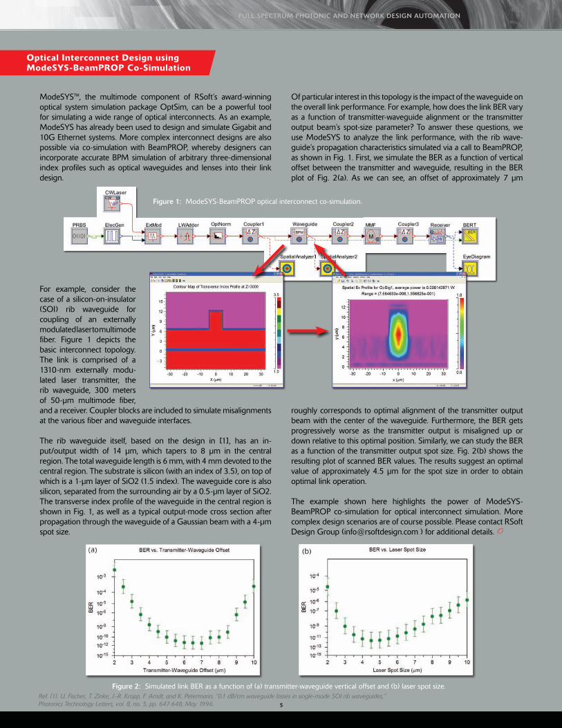
Of particular interest in this topology is the impact of the waveguide on the overall link performance. For example, how does the link BER vary as a function of transmitter-waveguide alignment or the transmitter output beam’s spot-size parameter? To answer these questions, we use ModeSYS to analyze the link performance, with the rib wave-guide’s propagation characteristics simulated via a call to BeamPROP, as shown in Fig. 1. First, we simulate the BER as a function of vertical offset between the transmitter and waveguide, resulting in the BER plot of Fig. 2(a). As we can see, an offset of approximately 7 µm
roughly corresponds to optimal alignment of the transmitter output beam with the center of the waveguide. Furthermore, the BER gets progressively worse as the transmitter output is misaligned up or down relative to this optimal position. Similarly, we can study the BER as a function of the transmitter output spot size. Fig. 2(b) shows the resulting plot of scanned BER values. The results suggest an optimal value of approximately 4.5 µm for the spot size in order to obtain optimal link operation.
The example shown here highlights the power of ModeSYS-BeamPROP co-simulation for optical interconnect simulation. More complex design scenarios are of course possible. Please contact RSoft Design Group ([email protected] ) for additional details.
ModeSYS™, the multimode component of RSoft’s award-winning optical system simulation package OptSim, can be a powerful tool for simulating a wide range of optical interconnects. As an example, ModeSYS has already been used to design and simulate Gigabit and 10G Ethernet systems. More complex interconnect designs are also possible via co-simulation with BeamPROP, whereby designers can incorporate accurate BPM simulation of arbitrary three-dimensional index profiles such as optical waveguides and lenses into their link design.
For example, consider the case of a silicon-on-insulator (SOI) rib waveguide for coupling of an externally modulated laser to multimode fiber. Figure 1 depicts the basic interconnect topology. The link is comprised of a 1310-nm externally modu-lated laser transmitter, the rib waveguide, 300 meters of 50-µm multimode fiber, and a receiver. Coupler blocks are included to simulate misalignments at the various fiber and waveguide interfaces.
The rib waveguide itself, based on the design in [1], has an in-put/output width of 14 µm, which tapers to 8 µm in the central region. The total waveguide length is 6 mm, with 4 mm devoted to the central region. The substrate is silicon (with an index of 3.5), on top of which is a 1-µm layer of SiO2 (1.5 index). The waveguide core is also silicon, separated from the surrounding air by a 0.5-µm layer of SiO2.The transverse index profile of the waveguide in the central region is shown in Fig. 1, as well as a typical output-mode cross section after propagation through the waveguide of a Gaussian beam with a 4-µm spot size.
The solar cell studied here consists of a simple single-layer AR coating, a silicon absorbing region with frequency-dependent absorption [2], a silicon rectangular diffraction grating, and a DBR reflector composed of Si/SiO² layers. While thin-film devices can usually be designed via simple analytical formulas, ray-based optics cannot be used to model diffractive gratings, and a more rigorous approach is required. A simulation tool such as RSoft’s Diffract-MOD, which is based on Rigorous Coupled Wave Analysis (RCWA), provides a full-vector solution to model the electro-magnetic fields within the structure and to compute the absorption spectrum, A(λ), of this device. Given this spectrum and the incident solar spectrum S(λ) (see Figure 2), the total number of photons absorbed is given by the expression:
Once the number of photons absorbed is found, the short-circuit current density Jsc and open circuit voltage Voc can be computed as described in [1]. The solar cell efficiency η is given by the expression:
where Γf is a fill factor and Pin is the total input power.
RSoft’s scanning and optimization tool, MOST™, was configured using a custom post-processing script to automatically compute this efficiency from the absorption spectrum found by DiffractMOD, and then vary selected structural parameters to produce an optimized design. First, the solar cell efficiency was computed with-out the grating and DBR, and efficiencies of approximately 12% and 15% were found for silicon thicknesses of 5 and 10 µm respectively. Figure 3 shows simulation results of the cell efficiency for different refractive indices of the AR coating and for different grating periods, both with the DBR: efficiencies of approximately 17% and 19% were found, showing an increase.
The simulation results in this case show that it is possible to use a light-trapping diffraction grating to increase the efficiency of thin-film crystalline silicon solar cells. RSoft’s DiffractMOD simulation tool is well suited for the simple and accurate modeling this type of structure. When used in conjunction with MOST, custom post-processing can be performed to create user-defined data output. Furthermore, MOST can be used to find optimal values for any structural parameters.
4 5
Modeling High-Efficiency Solar Cells with DiffractMOD and MOST
Optical Interconnect Design using ModeSYS-BeamPROP Co-Simulation
FULL SPECTRUM PHOTONIC AND NETWORK DESIGN AUTOMATION FULL SPECTRUM PHOTONIC AND NETWORK DESIGN AUTOMATION
Solar Cell Efficiency vs. Diffraction Grating Period
Diffraction Grating Period0 1 2 3
Cel
l Effi
cien
cy [%
]
15
16
17
18
19Si Thickness = 5μm
Si Thickness = 10μm
Normalized DiffractMOD Absorption Spectrum
FIG 2FIG 1
Wavelength(μm) 0.3 0.4 0.5 0.6 0.7 0.8 0.9 1.0 1.1 1.2
Spec
tral I
rradi
ance
[W/(m
2 mm
1 )]
0.0
0.2
0.4
0.6
0.8
1.0
1.2
1.4 Solar Spectrumat Sea Level
Normalized DiffractMODAbsorption Spectrum
Solar Cell Efficiency vs. Refractive Index of AR Coating
Refractive Index of AR Layer1.4 1.5 1.6 1.7 1.8 1.9 2.0 2.1 2.2 2.3 2.4
Cel
l Effi
cien
cy [%
]
15
16
17
18
19Si Thickness = 5 μm
Si Thickness = 10 μm
Incident Solar Light
Anti-ReflectionCoating
Silicon
DBR Reflector
Figure 1: Schematic of Thin-Film solar Cell with Diffractive Grating and DBR.
Figure 3: Optimization results showing the solar cell efficiency as a function of a) the refractiveindex of the AR layer, and b) the period of the diffraction grating. Results for silicon thicknesses of 5 and 10 µm are shown.
Nc =1 ∫ A(λ)S(λ)λdλ
ħc
η =JscVocΓƒ
Pin
a)
b)
Figure 2: Comparison of the solar spectrum at sea level (AM 1.5) and a spectrum computed by DiffractMOD. The DiffractMOD results have been normalized to the solar spectrum.
Figure 1: ModeSYS-BeamPROP optical interconnect co-simulation.
Figure 2: Simulated link BER as a function of (a) transmitter-waveguide vertical offset and (b) laser spot size.Ref. [1] 1N. N. Feng, J. Michel, L. Zeng, J. Liu, C. Hong, L. C. Kimerling, and X. Duan, “Design of highly efficient light-trapping structure for thin-film crystalline silicon solar cells,” IEEE Trans. on Electron Devices, Vol. 54, No. 8, August, 2007.
Ref. [2] E. D. Palik, Handbook of optical constants of solids, Academic Press, 1985. Ref. [1]. U. Fischer, T. Zinke, J.-R. Kropp, F. Arndt, and K. Petermann, “0.1 dB/cm waveguide losses in single-mode SOI rib waveguides,” Photonics Technology Letters, vol. 8, no. 5, pp. 647-648, May 1996.
Renewable energy sources such as solar energy have the potential to radically change the way the world’s energy needs are met. Thin-film crystalline silicon solar cells promise to be a major part of future solar cell technology since they have a low cost and can be easily fabricated with existing semiconductor technology. One drawback to thin-film solar cells is a fairly low efficiency since the majority of photons pass through the silicon layer without being absorbed; the thickness of the silicon is usually less than the absorption length. This article will explore the addition of a diffractive reflection grating and Distributed Bragg Reflector (DBR) to the design as described in Ref [1] to effectively trap light within the structure resulting in a significant efficiency improvement.
In their simplest form, thin-film solar cells are usually composed of an antireflection (AR) coating to allow light to enter the device with minimal loss, a photon-absorbing silicon region that produces the electrical output, and a reflector. This reflector effectively doubles the optical path length and allows the light to pass through the silicon a second time. The efficiency of this basic design depends on the quality of the AR coating and the thickness of the silicon region; a thicker region generally allows for more absorption. Unfortunately, the more silicon used, the more expensive and heavy the device is. An elegant solution to this problem is to replace the reflector with a DBR and to add a diffractive grating. The diffractive grating will scatter the light into different diffractive orders within the silicon region, effectively trapping photons within the device as shown in Figure 1. In order to be effective, the design specifics of the AR coating, diffractive grating, and DBR must all be optimized for the entire solar spectrum.
Of particular interest in this topology is the impact of the waveguide on the overall link performance. For example, how does the link BER vary as a function of transmitter-waveguide alignment or the transmitter output beam’s spot-size parameter? To answer these questions, we use ModeSYS to analyze the link performance, with the rib wave-guide’s propagation characteristics simulated via a call to BeamPROP, as shown in Fig. 1. First, we simulate the BER as a function of vertical offset between the transmitter and waveguide, resulting in the BER plot of Fig. 2(a). As we can see, an offset of approximately 7 µm
roughly corresponds to optimal alignment of the transmitter output beam with the center of the waveguide. Furthermore, the BER gets progressively worse as the transmitter output is misaligned up or down relative to this optimal position. Similarly, we can study the BER as a function of the transmitter output spot size. Fig. 2(b) shows the resulting plot of scanned BER values. The results suggest an optimal value of approximately 4.5 µm for the spot size in order to obtain optimal link operation.
The example shown here highlights the power of ModeSYS-BeamPROP co-simulation for optical interconnect simulation. More complex design scenarios are of course possible. Please contact RSoft Design Group ([email protected] ) for additional details.
ModeSYS™, the multimode component of RSoft’s award-winning optical system simulation package OptSim, can be a powerful tool for simulating a wide range of optical interconnects. As an example, ModeSYS has already been used to design and simulate Gigabit and 10G Ethernet systems. More complex interconnect designs are also possible via co-simulation with BeamPROP, whereby designers can incorporate accurate BPM simulation of arbitrary three-dimensional index profiles such as optical waveguides and lenses into their link design.
For example, consider the case of a silicon-on-insulator (SOI) rib waveguide for coupling of an externally modulated laser to multimode fiber. Figure 1 depicts the basic interconnect topology. The link is comprised of a 1310-nm externally modu-lated laser transmitter, the rib waveguide, 300 meters of 50-µm multimode fiber, and a receiver. Coupler blocks are included to simulate misalignments at the various fiber and waveguide interfaces.
The rib waveguide itself, based on the design in [1], has an in-put/output width of 14 µm, which tapers to 8 µm in the central region. The total waveguide length is 6 mm, with 4 mm devoted to the central region. The substrate is silicon (with an index of 3.5), on top of which is a 1-µm layer of SiO2 (1.5 index). The waveguide core is also silicon, separated from the surrounding air by a 0.5-µm layer of SiO2.The transverse index profile of the waveguide in the central region is shown in Fig. 1, as well as a typical output-mode cross section after propagation through the waveguide of a Gaussian beam with a 4-µm spot size.
The solar cell studied here consists of a simple single-layer AR coating, a silicon absorbing region with frequency-dependent absorption [2], a silicon rectangular diffraction grating, and a DBR reflector composed of Si/SiO² layers. While thin-film devices can usually be designed via simple analytical formulas, ray-based optics cannot be used to model diffractive gratings, and a more rigorous approach is required. A simulation tool such as RSoft’s Diffract-MOD, which is based on Rigorous Coupled Wave Analysis (RCWA), provides a full-vector solution to model the electro-magnetic fields within the structure and to compute the absorption spectrum, A(λ), of this device. Given this spectrum and the incident solar spectrum S(λ) (see Figure 2), the total number of photons absorbed is given by the expression:
Once the number of photons absorbed is found, the short-circuit current density Jsc and open circuit voltage Voc can be computed as described in [1]. The solar cell efficiency η is given by the expression:
where Γf is a fill factor and Pin is the total input power.
RSoft’s scanning and optimization tool, MOST™, was configured using a custom post-processing script to automatically compute this efficiency from the absorption spectrum found by DiffractMOD, and then vary selected structural parameters to produce an optimized design. First, the solar cell efficiency was computed with-out the grating and DBR, and efficiencies of approximately 12% and 15% were found for silicon thicknesses of 5 and 10 µm respectively. Figure 3 shows simulation results of the cell efficiency for different refractive indices of the AR coating and for different grating periods, both with the DBR: efficiencies of approximately 17% and 19% were found, showing an increase.
The simulation results in this case show that it is possible to use a light-trapping diffraction grating to increase the efficiency of thin-film crystalline silicon solar cells. RSoft’s DiffractMOD simulation tool is well suited for the simple and accurate modeling this type of structure. When used in conjunction with MOST, custom post-processing can be performed to create user-defined data output. Furthermore, MOST can be used to find optimal values for any structural parameters.
4 5
Modeling High-Efficiency Solar Cells with DiffractMOD and MOST
Optical Interconnect Design using ModeSYS-BeamPROP Co-Simulation
FULL SPECTRUM PHOTONIC AND NETWORK DESIGN AUTOMATION FULL SPECTRUM PHOTONIC AND NETWORK DESIGN AUTOMATION
Solar Cell Efficiency vs. Diffraction Grating Period
Diffraction Grating Period0 1 2 3
Cel
l Effi
cien
cy [%
]
15
16
17
18
19Si Thickness = 5μm
Si Thickness = 10μm
Normalized DiffractMOD Absorption Spectrum
FIG 2FIG 1
Wavelength(μm) 0.3 0.4 0.5 0.6 0.7 0.8 0.9 1.0 1.1 1.2
Spec
tral I
rradi
ance
[W/(m
2 mm
1 )]
0.0
0.2
0.4
0.6
0.8
1.0
1.2
1.4 Solar Spectrumat Sea Level
Normalized DiffractMODAbsorption Spectrum
Solar Cell Efficiency vs. Refractive Index of AR Coating
Refractive Index of AR Layer1.4 1.5 1.6 1.7 1.8 1.9 2.0 2.1 2.2 2.3 2.4
Cel
l Effi
cien
cy [%
]
15
16
17
18
19Si Thickness = 5 μm
Si Thickness = 10 μm
Incident Solar Light
Anti-ReflectionCoating
Silicon
DBR Reflector
Figure 1: Schematic of Thin-Film solar Cell with Diffractive Grating and DBR.
Figure 3: Optimization results showing the solar cell efficiency as a function of a) the refractiveindex of the AR layer, and b) the period of the diffraction grating. Results for silicon thicknesses of 5 and 10 µm are shown.
Nc =1 ∫ A(λ)S(λ)λdλ
ħc
η =JscVocΓƒ
Pin
a)
b)
Figure 2: Comparison of the solar spectrum at sea level (AM 1.5) and a spectrum computed by DiffractMOD. The DiffractMOD results have been normalized to the solar spectrum.
Solar Cell Efficiency vs. Diffraction Grating Period
Diffraction Grating Period0 1 2 3
Cel
l Effi
cien
cy [%
]
15
16
17
18
19Si Thickness = 5μm
Si Thickness = 10μm
Normalized DiffractMOD Absorption Spectrum
FIG 2FIG 1
Wavelength(μm) 0.3 0.4 0.5 0.6 0.7 0.8 0.9 1.0 1.1 1.2
Spec
tral I
rradi
ance
[W/(m
2 mm
1 )]
0.0
0.2
0.4
0.6
0.8
1.0
1.2
1.4 Solar Spectrumat Sea Level
Normalized DiffractMODAbsorption Spectrum
Solar Cell Efficiency vs. Refractive Index of AR Coating
Refractive Index of AR Layer1.4 1.5 1.6 1.7 1.8 1.9 2.0 2.1 2.2 2.3 2.4
Cel
l Effi
cien
cy [%
]
15
16
17
18
19Si Thickness = 5 μm
Si Thickness = 10 μm
Incident Solar Light
Anti-ReflectionCoating
Silicon
DBR Reflector
Figure 1: Schematic of Thin-Film solar Cell with Diffractive Grating and DBR.
Figure 3: Optimization results showing the solar cell efficiency as a function of a) the refractiveindex of the AR layer, and b) the period of the diffraction grating. Results for silicon thicknesses of 5 and 10 µm are shown.
Nc =1 ∫ A(λ)S(λ)λdλ
ħc
η =JscVocΓƒ
Pin
a)
b)
Figure 2: Comparison of the solar spectrum at sea level (AM 1.5) and a spectrum computed by DiffractMOD. The DiffractMOD results have been normalized to the solar spectrum.
Solar Cell Efficiency vs. Diffraction Grating Period
Diffraction Grating Period0 1 2 3
Cel
l Effi
cien
cy [%
]
15
16
17
18
19Si Thickness = 5μm
Si Thickness = 10μm
Normalized DiffractMOD Absorption Spectrum
FIG 2FIG 1
Wavelength(μm) 0.3 0.4 0.5 0.6 0.7 0.8 0.9 1.0 1.1 1.2
Spec
tral I
rradi
ance
[W/(m
2 mm
1 )]
0.0
0.2
0.4
0.6
0.8
1.0
1.2
1.4 Solar Spectrumat Sea Level
Normalized DiffractMODAbsorption Spectrum
Solar Cell Efficiency vs. Refractive Index of AR Coating
Refractive Index of AR Layer1.4 1.5 1.6 1.7 1.8 1.9 2.0 2.1 2.2 2.3 2.4
Cel
l Effi
cien
cy [%
]
15
16
17
18
19Si Thickness = 5 μm
Si Thickness = 10 μm
Incident Solar Light
Anti-ReflectionCoating
Silicon
DBR Reflector
Figure 1: Schematic of Thin-Film solar Cell with Diffractive Grating and DBR.
Figure 3: Optimization results showing the solar cell efficiency as a function of a) the refractiveindex of the AR layer, and b) the period of the diffraction grating. Results for silicon thicknesses of 5 and 10 µm are shown.
Nc =1 ∫ A(λ)S(λ)λdλ
ħc
η =JscVocΓƒ
Pin
a)
b)
Figure 2: Comparison of the solar spectrum at sea level (AM 1.5) and a spectrum computed by DiffractMOD. The DiffractMOD results have been normalized to the solar spectrum.
Solar Cell Efficiency vs. Diffraction Grating Period
Diffraction Grating Period0 1 2 3
Cel
l Effi
cien
cy [%
]
15
16
17
18
19Si Thickness = 5μm
Si Thickness = 10μm
Normalized DiffractMOD Absorption Spectrum
FIG 2FIG 1
Wavelength(μm) 0.3 0.4 0.5 0.6 0.7 0.8 0.9 1.0 1.1 1.2
Spec
tral I
rradi
ance
[W/(m
2 mm
1 )]
0.0
0.2
0.4
0.6
0.8
1.0
1.2
1.4 Solar Spectrumat Sea Level
Normalized DiffractMODAbsorption Spectrum
Solar Cell Efficiency vs. Refractive Index of AR Coating
Refractive Index of AR Layer1.4 1.5 1.6 1.7 1.8 1.9 2.0 2.1 2.2 2.3 2.4
Cel
l Effi
cien
cy [%
]
15
16
17
18
19Si Thickness = 5 μm
Si Thickness = 10 μm
Incident Solar Light
Anti-ReflectionCoating
Silicon
DBR Reflector
Figure 1: Schematic of Thin-Film solar Cell with Diffractive Grating and DBR.
Figure 3: Optimization results showing the solar cell efficiency as a function of a) the refractiveindex of the AR layer, and b) the period of the diffraction grating. Results for silicon thicknesses of 5 and 10 µm are shown.
Nc =1 ∫ A(λ)S(λ)λdλ
ħc
η =JscVocΓƒ
Pin
a)
b)
Figure 2: Comparison of the solar spectrum at sea level (AM 1.5) and a spectrum computed by DiffractMOD. The DiffractMOD results have been normalized to the solar spectrum.
Solar Cell Efficiency vs. Diffraction Grating Period
Diffraction Grating Period0 1 2 3
Cel
l Effi
cien
cy [%
]
15
16
17
18
19Si Thickness = 5μm
Si Thickness = 10μm
Normalized DiffractMOD Absorption Spectrum
FIG 2FIG 1
Wavelength(μm) 0.3 0.4 0.5 0.6 0.7 0.8 0.9 1.0 1.1 1.2
Spec
tral I
rradi
ance
[W/(m
2 mm
1 )]
0.0
0.2
0.4
0.6
0.8
1.0
1.2
1.4 Solar Spectrumat Sea Level
Normalized DiffractMODAbsorption Spectrum
Solar Cell Efficiency vs. Refractive Index of AR Coating
Refractive Index of AR Layer1.4 1.5 1.6 1.7 1.8 1.9 2.0 2.1 2.2 2.3 2.4
Cel
l Effi
cien
cy [%
]
15
16
17
18
19Si Thickness = 5 μm
Si Thickness = 10 μm
Incident Solar Light
Anti-ReflectionCoating
Silicon
DBR Reflector
Figure 1: Schematic of Thin-Film solar Cell with Diffractive Grating and DBR.
Figure 3: Optimization results showing the solar cell efficiency as a function of a) the refractiveindex of the AR layer, and b) the period of the diffraction grating. Results for silicon thicknesses of 5 and 10 µm are shown.
Nc =1 ∫ A(λ)S(λ)λdλ
ħc
η =JscVocΓƒ
Pin
a)
b)
Figure 2: Comparison of the solar spectrum at sea level (AM 1.5) and a spectrum computed by DiffractMOD. The DiffractMOD results have been normalized to the solar spectrum.
Figure 1: ModeSYS-BeamPROP optical interconnect co-simulation.
Figure 2: Simulated link BER as a function of (a) transmitter-waveguide vertical offset and (b) laser spot size.Ref. [1] 1N. N. Feng, J. Michel, L. Zeng, J. Liu, C. Hong, L. C. Kimerling, and X. Duan, “Design of highly efficient light-trapping structure for thin-film crystalline silicon solar cells,” IEEE Trans. on Electron Devices, Vol. 54, No. 8, August, 2007.
Ref. [2] E. D. Palik, Handbook of optical constants of solids, Academic Press, 1985. Ref. [1]. U. Fischer, T. Zinke, J.-R. Kropp, F. Arndt, and K. Petermann, “0.1 dB/cm waveguide losses in single-mode SOI rib waveguides,” Photonics Technology Letters, vol. 8, no. 5, pp. 647-648, May 1996.

to differentiate different types of traffic. The MAC protocol at the node object is subdivided into Access Strategy, Fairness Control and Reser-vation Strategy. The network object models the network transmission. It transmits data packets, control messages and setup messages. To guarantee fair access to all nodes, a control schema called multi-meta ring is also implemented. This multi-meta ring circulates one control message across the ring, which travels in the opposite direction of the data traffic. Figure 2 shows the transmission queue latency of packets from client node to client node.
The avionic WDM LAN simulation pro- ject is a part of our STTR contract for which RSoft Design Group has partnered with the University of California, Santa Barbara and the University of Florida, Gainesville.
devices can be achieved by considering these limitations from the start of the design process so that their impact on device perfor-mance can be reduced. This type of design process requires an optimal balance between design and manufacturing to result in optical components that have high performance and are cheap to create. This requires an optimal balance between design and manu-facturing to result optical components that have high performance with low cost.
RSoft: Why did you decide to work with RSoft Design Group for design and simulation software?
DNP: Currently, we use RSoft’s BeamPROP™ and DiffractMOD™ packages. Both of these tools share the same CAD interface for device layout, which provides a unified environment for propaga-tion analysis with BeamPROP and diffraction analysis with Diffract-MOD. Furthermore, the CAD allows us to define the cross-section of the components via a data file, which provides a convenient way to define manufacturing errors. Our designers find this setup extremely convenient.
RSoft: What do you see as industry needs and demands for photonic modeling software for the next generation applications?
DNP: Simulations which accurately represent the real world are quite complex, and may require more than one simulation tool. For example, the performance of devices made from the diffract components need to be evaluated in conjunction with another device, such as a femtosecond laser. I see the optical design industry moving towards a more integrated approach to correctly model these types of situations.
RSoft: Thank you. We wish you the best of luck in your research.
6 3
RSoft: Please tell us about Dai Nippon Printing (DNP).
DNP: Established in 1876, DNP was the first full-scale printing company in Japan. Expanding printing technology has been a fundamental part of DNP’s mission since the 1950s; it’s business not only limited in the printing of books and magazines, but has diversified. It now includes a wide variety of everyday materials such as wallpaper, electronic materials such as large display color filters, and photomasks for the semiconductor manufacturing process. By combining innovative technology and technical expertise, DNP offers products and services that can help fulfill dreams, enrich everyday life, and enhance communication.
RSoft: Can you tell us about your current research?
DNP: I am currently researching the manufacturing process used to create multiple section diffraction components. Improved manu-facturing techniques allow components to be created with accuracy within a few nanometers. These ultra-high resolution components are created with photomasks made from highly uniform and extremely flat synthesized quartz silicon. This process is studied to determine the trade-offs between manufacturing limitations and device performance. I am also studying the relationship between measurement results and design characteristics to improve the design and manufacturing process.
RSoft: What kinds of challenges do you face in your research?
DNP: A common misconception about the design and manufac-ture of optical components is that any level of performance can be reached if enough money is spent. Unfortunately, limitations imposed by materials and manufacturing processes can cause errors. Given this reality, ultra-high resolution, high performance
Mr. Nobuhito Toyama
RSoft Interview with Mr. Nobuhito Toyama, Dai Nippon Printing (DNP)
Mr. Nobuhito Toyama joined Dai Nippon Printing (DNP) in the early 1990s, and is involved in the research and development of one of DNP’s key technologies: the semiconductor photomask manufacturing process for optical components. His group at DNP is primarily studying diffraction components and are investigating the trade-off between desired device performances and manu-facturing limitations using both design results and measurement results. They are also developing next generation complex nano-imprinting technology for imaging applications based on the semiconductor photomask process and the productivity with replication by nanoimprinting.
As part of the effort to upgrade existing avionic data networks, future avionic fiber-optic systems will rely on switched Wavelength Division Multiplexing (WDM) Local Area Network (LAN) architec-tures for reliable high-speed data transmission. Fiber optic systems have some inherent advantages over the existing copper based systems. An important advantage is that the fiber physical plant has less weight/volume compared to the copper physical plant. Other key advantages are higher bandwidth, resilient to EMI and protocol independence.
Research activities in developing WDM LAN deal with a significant number of design and optimization issues at both the physical and logical layers of the network. While physical-layer simulation of the network is critical for assessing the network performance as a function of detailed device characteristics, logical-level analysis is equally important in order to evaluate different network topologies, new protocols for efficient routing in a multi-wavelength system, and control plane mechanisms for network management. We have developed a new set of applications in our discrete event simula-tion software, Artifex™, to model the logical level of WDM LAN in aerospace platforms.
One of the applications deals with implementing a new Media Access Control (MAC) protocol. In this application, we simulated a WDM LAN with nodes having tunable lasers and fixed receivers. Each node receives data on a particular wavelength from all other nodes. Multiple transmitters sending data at the same time on a single wavelength creates a shared medium, so a MAC protocol needs to be developed. The model shown in Fig 1 is the logical view of a 16 nodes WDM ring. There are two objects in this network, the Node object and the Network object. Each node generates packets for each wavelength channel based on a specified traffic distribution model. The packets can also be configured with a priority of service
Photodetectors are an important component in photonics; covering a wide variety of applications from thermal imaging to telecommuni-cations. They operate over various spectral ranges and bandwidths, employing a wide variety of material systems including silicon, AlGaAs, GaInAsSb, and InGaNAs to name a few. Many structural features have been found to improve the efficiency of these devices, such as DBRs, surface gratings, and the growth of a black silicon layer (silicon detectors).
Recently, LaserMOD™ has been extended to accommodate surface normal photodetectors (PDs) and solar cells. For a given growth structure such p-n, pin, and quantum-well device, the internal optical field, established by incident power at a given wavelength, is calculated self-consistently with the carrier transport governed by a particular set of bias conditions. The figures below show the simula-tion results of a simple AlGaAs pin photodiode. Steady-state results show the reverse bias IV curves with breakdown at several incident power levels, and transient results show the pulse response to a small input signal.
Surface Normal AlGaAs 830nm Photo-Diode
WDM LAN Simulations for Aerospace Platforms
FULL SPECTRUM PHOTONIC AND NETWORK DESIGN AUTOMATION FULL SPECTRUM PHOTONIC AND NETWORK DESIGN AUTOMATION
Current vs Voltage
Voltage (V)50- 40- 30- 20- 10- 0
Cur
rent
(mA)
0.015-
0.012-
0.009-
0.006-
0.003-
0.000 Legend:
3mW/cm2
35mW/cm2
177mW/cm2
Transient Response
Time (ps)0 100 200 300 400 500 600 700 800
Phot
o C
urre
nt
0.620
0.622
0.624
0.626
0.628
0.630
FIG 1 FIG 2
Current vs Voltage
Voltage (V)50- 40- 30- 20- 10- 0
Cur
rent
(mA)
0.015-
0.012-
0.009-
0.006-
0.003-
0.000 Legend:
3mW/cm2
35mW/cm2
177mW/cm2
Transient Response
Time (ps)0 100 200 300 400 500 600 700 800
Phot
o C
urre
nt
0.620
0.622
0.624
0.626
0.628
0.630
FIG 1 FIG 2
Figure 1. Reverse bias IV curves, including break-down, for incident 830nm light at different power levels.
Figure 2. Transient response of the detector to a small pulse perturbation of the incident optical power.
Figure 1: Logical view of 16 node WDM ring.
Figure 2: Shows the transmission queue latency of packets send from client node to client node.
RSoft Design @ California Polytechnic State University
During the last year, assistant Professor Xiaomin Jin at California Polytechnic State University (Cal Poly) has used RSoft’s LaserMOD and OptSim tools in her teaching classes and research projects. Recently, she has expanded her usage to RSoft’s passive device tools, such as DiffractMOD and FullWAVE. The photonics program at Cal Poly Electircal Engineering Department began in 1985 and a dedi-cated photonics lab was established with the assistance of HP and several other corporations. Currently, the department offers three lecture courses and two lab courses in fiber optics and photonic engineering that use RSoft’s software. Approximately 100 students enroll annually in these technical elective courses and at least 15 senior projects and 3 master’s theses are completed each year in the photonics area. These photonics courses are one of the most heavily subscribed elective courses in the electrical engineering program. Prof. Jin commented that: “The tools give a great platform for student research at our undergraduate teaching university, and fit well with Cal Poly’s emphasis of learning by experience. They help our students by providing standard math packages. Even though our students don’t have a strong numerical simulation background, they still can analyze and study the physics of advanced optoelectronic devices. Without these tools, it is hard for the students to get into advanced research areas. Additionally, the RSoft tools have helped our students publish several research papers within the last year on photo-detector design, GaN laser diode design, and GaN LED applications.“
Artifex in the Prairies
The object oriented Petri Net simulation engine Artifex can be found in many laboratories, including the Wireless Sensor Laboratory at the University of Manitoba in Winnipeg, Manitoba, Canada. The Laboratory was equipped through a number of grants, including a grant from Canada Foundation for Innovation (CFI) which put specific emphasis on a ten-seat license for Artifex. A small group of Artifex users, led by Prof. Jelena Misic and Prof. Vojislav B. Misic, model and analyze the performance of various communication and security protocols for wireless sensor and personal area networks.
“Artifex is a natural choice for modeling and performance analysis of various communication protocols,” says Vojislav who is a devoted Artifex fan since 1999. “It has an intuitive GUI front end, a small but powerful set of modeling operators, and a simulation engine that’s lightning-fast compared to more popular simulation engines such as ns-2. In addition, it is very reliable and uses memory efficiently; even large simulation experiments with models that include hundreds of nodes can be run in reasonable time, and there are virtually no mem-ory leaks or other implementation problems. And the compact model format allows for easy exchange and sharing of models among us, regardless of the hardware platform; in fact, most of our experiments now run on Windows XP boxes.” Jelena and Vojislav have done some pioneering research in the area of performance analysis of Bluetooth networks; their work has been published in many research articles in various journals and conferences, as well as in the book Performance Modeling and Analysis of Bluetooth Networks: Polling, Scheduling, and Traffic Control (Boca Raton, FL: Auerbach, 2005). Their current work in the Wireless Sensor Laboratory deals with various aspects of the recent IEEE 802.15.4 low rate wireless personal network commu-nication standard, including performance analysis, power manage-ment, and security. The results of this research will be summarized in the forthcoming book Wireless Personal Area Networks: Perfor-mance, Interconnections, and Security with IEEE 802.15.4, which is scheduled to appear in January 2008 with John Wiley & Sons.
FullWAVE and BandSOLVE in Edge Cutting Research of Metamaterial Photonic Crystals at Tohoku University
Associate Professor Hiroshi Miyazaki in the Department of Applied Physics, Tohoku University, is intensively working on the theoret-ical study of photonic crystals from the Terahertz region all the way to ultraviolet. He is especially interested in the establishment of an auto-
matic and general design policy for metamaterial photonic crystals which not only exhibit negative reflection but negative perme-ability as well. He is using RSoft’s FullWAVE and BandSOLVE™ simulation tools for these research tasks. Professor Miyazski commented that: “these tools are excellent in general and can be used for technological tasks such as the optimization of waveguide structures and the design of photonic crystals.” He also mentioned that people from different research areas would have different requests and needs for the software. And that RSoft is actively working with end users to meet specific research needs. “We look forward to more cooperation with RSoft to maximize the power that the numerical simulation tools offer.” Prof. Miyazaki said.
2 7
the A/D converter, the number of branch metric stages and the number of states are user-defined parameters. The processor uses an innovative square-root metric that decreases the computational complexity by assuming a stationary gaussian distribution over the square root of the signal.
OptSim’s unique capability of simulating arbitrarily long bit sequences and number of samples is the key enabler of MLSE system simulation. Given the nonlinear digital processing of the Viterbi algorithm based on the most-likely state sequence selection, there is no analytical expression available to assess the system per-formance. For this reason, the Monte-Carlo error counting approach is the only viable choice. With a target BER of 10^-4 the number of errors to ensure an estimated OSNR 95% confidence interval of ±0.15 db is about 100, thus bringing the required total number of simulated bit to over one million.
The system of Fig. 1 consists of a 10 Gbit/s (2^20-1) pseudorandom bit sequence (PRBS) generator followed by a 5-pole Bessel filter with a -3 dB bandwidth of 7.5 GHz. The signal at the output of the filter drives an ideal Mach-Zehnder modulator with infinite extinc-tion ratio and zero chirp. The fiber is 700 Km-long with a value of dispersion D equal to 16 ps/nm, typical of G.652 standard single-mode fiber at 1550 nm – the continuous-wave (CW) laser emission wavelength. At the receiver there is a second-order super-gaussian optical filter with a -3 dB bandwidth equal to 35 GHz, followed by an ideal photo-detector and a five-pole Bessel post-detection filter with a -3 dB bandwidth equal to 7.5 GHz. The MLSE Viterbi processor
uses 8192 states, 4 samples per bit, an A/D decoder with infinite resolution and a delay of 3N bits before making a bit-wise decision, where N is the number of states. This configuration is sufficient to compensate 11,200 ps/nm of total accumulated dispersion with a -3 dB OSNR penalty. Fig. 2 shows the BER vs. OSNR obtained with a Monte-Carlo error-counting approach over 1,048,576 simulated bits and 32 samples per bit. The target BER of 10^-4 is reached for an OSNR value equal to 13 dB.
In conclusion the new OptSim MLSE model enables the user to design and simulate direct-detection systems deploying MLSE-based receivers. The Monte-Carlo error counting is the only viable approach to calculate the system performance. OptSim’s unique capability of simulating arbitrarily long bit sequences enables the user to design systems with a line BER of 10^-3 to 10^-4, requiring simulations of over 1 million bits.
wave nature of light based on Maxwell’s equations, with regard to near-field interactions of closely spaced particles and coherent interference effects. This over-simplification leads to significant inaccuracies while characterizing light scattering by tissue and cellular structures. One of RSoft’s flagship tools FullWAVE™, is very well suited to accurately model the complexities of the biological tissue structure and its interaction with light. FullWAVE is based on the Finite-Difference Time-Domain (FDTD) algorithm, which is an ab-initio approach for direct numerical solution of time-dependent Maxwell’s equations, with no inherent approximations. FullWAVE also has a clustering option that can distribute the simulation workload over several computers in a network to result in faster and larger simulations.
Here we present two examples validating the effectiveness and accuracy of FullWAVE for such light scattering calculations. The first example computes the angular far-field distribution of light scattering from a single homogeneous sphere. The second example models the total scattering cross section (TSCS) spectra of a cluster of 19 randomly positioned spheres. The validation results of the FullWAVE simulations against the analytic methods are presented in the Figures 1 and 2; as can be seen the numerical results obtained via FullWAVE agree well with the analytical results. The spectral properties of TSCS, presented in Fig 2, are of particular importance in applications such as spectroscopic tissue diagnosis for early detection of pre-cancerous conditions, and can be easily obtained through standard FullWAVE analysis options.
Note that in our choice of examples we have restricted ourselves to simple cell morphologies; this is only in-order to be able to validate our results against analytic solutions based on the Mie theory and the Multi-sphere expansions respectively. However, as mentioned earlier due to the inherent ab-initio nature of FDTD, much more complicated cell-morphologies and structures (nonspherical/inhomogeneous) can be easily incorporated into the simulations.
The search for new optical methods for noninvasive biomedical diagnostics and the need to understand/improve the existing techniques, require simulation tools capable of accurately modeling the structural and morphological complexities of the biological tissue structures, without using questionable heuristic approximations. RSoft’s FullWAVE package provides an ideal platform, accurate and user-friendly, for a wide range of such biomedical applications.
Modeling Light Scattering from Biological ... continued from page 1
Maximum Likelihood Sequence... continued from page 1
Campus Corner
FULL SPECTRUM PHOTONIC AND NETWORK DESIGN AUTOMATION FULL SPECTRUM PHOTONIC AND NETWORK DESIGN AUTOMATION
Frequency [THz]0 100 200
TSC
S [a
.u.]
0
200
400
600
800
1000
1200Multisphere
FullWAVE
1.0
1.2Contour Map of Index Profile at Y=0
X (μm)
Z (μ
m)
5- 3- 1- 1 3 5
0
2
4
6
8
Scattering Angle (deg)0 20 40 60 80 100 120 140 160 180
log(
DSC
S)
13-
12-
11-
10-
9-
8-
7-Mie
FullWAVE
FIGURE 1: FullWAVE computed differential scattering cross-section (DSCS) as a function of angle validated against the analytic solution from Mie theory. The simulation parameters were as follows: diameter=8µm, index=1.2, λ=0.75µm.
FIGURE 2: FullWAVE computed TSCS spectra validated against the analytic solution fromMultisphere expansion. The parameters were as follows: the pattern is 19 randomly placed spheres within a 20µm diameter, individual sphere diameter=3µm, index=1.2.
8 9 10 11 12 13−4.5
−4
−3.5
−3
−2.5
−2
−1.5
OSNR [dB]
log 10
(BER
)
FIGURE 2: BER vs. OSNR for uncom-pensated transmis-sion at 10 Gbit/s over 700 Km SMF and 8192 state MLSE Viterbi pro-cessor, calculated with Monte-Carlo error counting over 1,048,576 simu-lated bits and 32 samples per bit.
Professor Hiroshi Miyazaki

For the fourth straight year, RSoft sponsored the Best Student PaperAwards at APOC November 1-5, 2007 at the Wuhan Science and Technology Convention and Exhi-bition Center in Wuhan, China. The Best Student Paper Awards were created to encourage participation and involvement of young engineers and scientists.
Also at APOC, our technical team submitted an invited paper, PhysicalLayer Modeling of Passive Optical Networks. RSoft authors include Jigesh Patel, Dwight Richards, Enrico Ghillino, Pablo Mena, Anil Panicker and Zhengyu Huang. The paper is available by contacting RSoft Design Group at [email protected]. The winning papers were:
Simulation and analysis of fiber Bragg grating-based Q-switched fiber laser with sidelobes’ influence consideration, by X. P. Cheng, Nanyang Technological Univ. (Singapore)
1.55 µm extremely efficient and polarization insensitive tunable Mach-Zehnder wavelength duplexer based on an InGaAsP/InP ridge waveguide structure, by L. Xu, Technische Univ. Eindhoven (Netherlands)
SBS based slow-light performance comparison of 10-Gb/s NRZ, PSBT and DPSK signals, by Lilin Yi, GET/Telecom Paris and Shanghai Jiao Tong Univ. (China)
A novel protection scheme for a hybrid WDM/TDM PON, by Jiajia Chen, RoyalInstitute of Technology KTH (Sweden) and Zhejiang Univ. (China).
Greg D. MillerCollinear CorporationUSA
Pu DonglinSuzhou UniversityChina
Lucia MarazziCoreComItaly
RSoft Co-sponsors Workshop on Optical Fibre Sensors and Components.
RSoft proudly co-sponsored the Workshop on Optical Fibre Sensors and Components, jointly organized by the British High Commission and the Indian Institute of Technology (IIT), Delhi at the British Council Auditorium in New Delhi, India. The three-day (December 7-9, 2006) work-shop brought together recognized international experts from the UK and their colleagues from India. The workshop provided a common platform to encourage Indo-British research and development co-operation in fibre optic sensors and guided wave opticalcomponent technologies. RSoft, being a global leader in providing photonic modeling tools for these technologies, always strives to help emerging econo-mies culminate their research from its nascency into an eventual industrial manufacturing phase.
APOC 2007 Best Student Paper AwardsSponsored by RSoft Design Group
REVIEWJANUARY-JUNE 2008 RSOFT DESIGN GROUP
VOLUME 7NUMBER 1
Modeling Light Scattering from Biological Cells and Cell-Clusters using Fullwave.
Electronic dispersion compensation (EDC) has recieved particular attention lately for its potential to correct for signal distortion in optical communication systems in the electrical domain after photo-detection, thereby promoting system cost savings and new network configurations with fewer regenera-tion sites. Types of linear and nonlinear distortion addressed by EDC include chromatic dispersion, polarization mode dispersion (PMD), modal dispersion and self-phase modulation (SPM).
The maximum likelihood sequence estimation (MLSE) represents a particularly promising version of EDC. In particular, this nonlin-ear equalization technique has performance advantages for the correction of chromatic dispersion distortions over other algorithms such as feed-forward equalization (FFE) and decision-feedback equalization (DFE). Recent simulation and experimental results have shown MLSE-based receivers to be capable of supporting uncompensated transmission over standard single-mode fiber exceeding 1,000 Km at 10 Gbit/s for a total accumulated disper-sion of over 17,000 ps/nm. In comparison FFE- and DFE- based receivers have been shown to be limited to dispersion values between 2,000 and 4,000 ps/nm.
OptSim™ includes a new advanced block implementing an efficient MLSE processor to be used in intensity-modulation direct-detection (IMDD) optical receivers. The model consists of an analog-to-digital (A/D) converter where samples are sent to a parallel bank of branch metric computation stages. The extracted metric is sent to a Viterbi processor, which uses a reduced-state algorithm. The resolution of
1
Spectral and angular properties of light scattered from biological tissue have been demonstrated to provide important diagnostic information of tissue and cellular structures on the micro and nano scales, with applications including but not limited to confocal and optical coherence tomography, light-scattering spectroscopy, spec-tral imaging, and flow cytometry. Moreover, it has been recently shown that observing the spectrum of back-reflected light from biological cell-clusters yields much more information regarding pre-cancerous conditions than any other minimally invasive optical technology. These advancements in optical tissue diagnostic technology have necessitated the need for rigorous simulation techniques capable of hand- ling such complex structures as the biological tissue.
Traditional simulation techniques that are used to study tissue optics treat tissue and cellular structures as homogeneous spheres.
These methods are unable to rigorously handle inhomogeneities in the cell morphology and structure, which have been shown to considerably effect the scattering properties. Moreover, these techniques generally neglect the full-vector electromagnetic
Maximum Likelihood Sequence Estimation (MLSE) Receiver for Uncompensated Transmission System Simulation in OptSim.
continued on page 2
continued on page 2
BRIEFS
8
FOE Tokyo Big Sight, Japan 16-18 January TBA*
Photonics WEST San Jose, California 22-24 January 907
Nano tech Tokyo Big Sight, Japan 13-15 February TBA*
OFC/OFOEC San Diego, California 26-28 February 1926
PV EXPO Tokyo Big Sight, Japan 27-29 February TBA*
Defense + Security Orlando, Florida 18-20 March 2016
Photonics Europe Strasbourg, France 8-10 April 320
Laser EXPO Tokyo Big Sight, Japan 23-25 April TBA*
CLEO San Jose, California 6-8 May 2216
ECIO Eindhoven, The Netherlands 11-13 June TBA*
UNITED STATES Corporate headquarters
Rsoft Design Group, Inc.400 Executive Boulevard, Ste. 100Ossining, NY 10562, USA
PHONE: 914.923.2164 E-MAIL: [email protected] WEB: www.rsoftdesign.com
JAPANRsoft Design Group Japan KKMatsura Building 2F, 1-9-6 Shiba Minato-ku, Tokyo, 105-0014 Japan
PHONE: + 81.3.5484.6670 EMAIL: [email protected]
EUROPERSoft Design UK, Ltd.11 Swinborne DriveSpringwood Industrial EstateBraintree, Essex CM7 2YP
PHONE: 44 (0)1376 528556 EMAIL: [email protected]
Visit us at the following tradeshows – 2008 FIRST HALF
SHOW LOCATION DATE BOOTH #
– 2008 FIRST HALF
FIGURE 1: OptSim project layout of a direct-detection system with uncompen-sated transmission at 10 Gbit/s over 700 Km G.652 fiber deploying a 8192 state MLSE Viterbi processor at the receiver. The eye diagram appears to be completely closed.
Frequency [THz]0 100 200
TSC
S [a
.u.]
0
200
400
600
800
1000
1200Multisphere
FullWAVE
1.0
1.2Contour Map of Index Profile at Y=0
X (μm)
Z (μ
m)
5- 3- 1- 1 3 5
0
2
4
6
8
Scattering Angle (deg)0 20 40 60 80 100 120 140 160 180
log(
DSC
S)
13-
12-
11-
10-
9-
8-
7-Mie
FullWAVE
FIGURE 1: FullWAVE computed differential scattering cross-section (DSCS) as a function of angle validated against the analytic solution from Mie theory. The simulation parameters were as follows: diameter=8µm, index=1.2, λ=0.75µm.
FIGURE 2: FullWAVE computed TSCS spectra validated against the analytic solution fromMultisphere expansion. The parameters were as follows: the pattern is 19 randomly placed spheres within a 20µm diameter, individual sphere diameter=3µm, index=1.2.
iPod Winners from the Survey!
*Please check our website for the latest tradeshow information.


![16th APOC Goa, India - asiapacificoptometry.orgasiapacificoptometry.org/doc/16th-APOC-Goa-India.pdf16th APOC Goa, India - Come to India Education - Conference Programme [new] - Invited](https://static.fdocuments.us/doc/165x107/5b2738237f8b9a42708b4b3f/16th-apoc-goa-india-apoc-goa-india-come-to-india-education-conference-programme.jpg)