AP32072 PCM Codec Connection to TC1130 - infineon.com
93
Never stop thinking. Microcontrollers Application Note, V 1.0, Nov 2004 PCM Codec Connection to TC1130 AP32072
Transcript of AP32072 PCM Codec Connection to TC1130 - infineon.com

N e v e r s t o p t h i n k i n g .
Microcontrol lers
Appl icat ion Note, V 1.0, Nov 2004
PCM Codec Connect ion to TC1130
AP32072

Controller Area Network (CAN): License of Robert Bosch GmbH
PCM Codec Connection to TC1130 Revision History: 2005-01 V 1.0
Previous Version: -
Page Subjects (major changes since last revision)
We Listen to Your CommentsAny information within this document that you feel is wrong, unclear or missing at all? Your feedback will help us to continuously improve the quality of this document. Please send your proposal (including a reference to this document) to:[email protected]
Edition 2005-01
Published by Infineon Technologies AG 81726 München, Germany
© Infineon Technologies AG 2006. All Rights Reserved.
LEGAL DISCLAIMER THE INFORMATION GIVEN IN THIS APPLICATION NOTE IS GIVEN AS A HINT FOR THE IMPLEMENTATION OF THE INFINEON TECHNOLOGIES COMPONENT ONLY AND SHALL NOT BE REGARDED AS ANY DESCRIPTION OR WARRANTY OF A CERTAIN FUNCTIONALITY, CONDITION OR QUALITY OF THE INFINEON TECHNOLOGIES COMPONENT. THE RECIPIENT OF THIS APPLICATION NOTE MUST VERIFY ANY FUNCTION DESCRIBED HEREIN IN THE REAL APPLICATION. INFINEON TECHNOLOGIES HEREBY DISCLAIMS ANY AND ALL WARRANTIES AND LIABILITIES OF ANY KIND (INCLUDING WITHOUT LIMITATION WARRANTIES OF NON-INFRINGEMENT OF INTELLECTUAL PROPERTY RIGHTS OF ANY THIRD PARTY) WITH RESPECT TO ANY AND ALL INFORMATION GIVEN IN THIS APPLICATION NOTE.
Information For further information on technology, delivery terms and conditions and prices please contact your nearest Infineon Technologies Office (www.infineon.com).
Warnings
Due to technical requirements components may contain dangerous substances. For information on the types in question please contact your nearest Infineon Technologies Office. Infineon Technologies Components may only be used in life-support devices or systems with the express written approval of Infineon Technologies, if a failure of such components can reasonably be expected to cause the failure of that life-support device or system, or to affect the safety or effectiveness of that device or system. Life support devices or systems are intended to be implanted in the human body, or to support and/or maintain and sustain and/or protect human life. If they fail, it is reasonable to assume that the health of the user or other persons may be endangered.

AP32072PCM Codec Connection to TC1130
1 Abstract . . . . . . . . . . . . . . . . . . . . . . . . . . . . . . . . . . . . . . . . . . . . . . . . . . . 4
2 Introduction . . . . . . . . . . . . . . . . . . . . . . . . . . . . . . . . . . . . . . . . . . . . . . . . 52.1 PCM Stream . . . . . . . . . . . . . . . . . . . . . . . . . . . . . . . . . . . . . . . . . . . . . . . . 62.2 SSC Features . . . . . . . . . . . . . . . . . . . . . . . . . . . . . . . . . . . . . . . . . . . . . . . 82.3 The Clock Generation . . . . . . . . . . . . . . . . . . . . . . . . . . . . . . . . . . . . . . . . . 9
3 HW Description . . . . . . . . . . . . . . . . . . . . . . . . . . . . . . . . . . . . . . . . . . . . 123.1 General . . . . . . . . . . . . . . . . . . . . . . . . . . . . . . . . . . . . . . . . . . . . . . . . . . . 123.2 Connection Example . . . . . . . . . . . . . . . . . . . . . . . . . . . . . . . . . . . . . . . . . 13
4 SW Description . . . . . . . . . . . . . . . . . . . . . . . . . . . . . . . . . . . . . . . . . . . . 154.1 SW Architecture . . . . . . . . . . . . . . . . . . . . . . . . . . . . . . . . . . . . . . . . . . . . . 154.1.1 Clock Generation . . . . . . . . . . . . . . . . . . . . . . . . . . . . . . . . . . . . . . . . . . 154.1.2 Data output . . . . . . . . . . . . . . . . . . . . . . . . . . . . . . . . . . . . . . . . . . . . . . 164.1.3 Chip Select Generation . . . . . . . . . . . . . . . . . . . . . . . . . . . . . . . . . . . . . 174.1.4 Input Handling . . . . . . . . . . . . . . . . . . . . . . . . . . . . . . . . . . . . . . . . . . . . 194.2 SW Implementation . . . . . . . . . . . . . . . . . . . . . . . . . . . . . . . . . . . . . . . . . . 214.2.1 Configuration . . . . . . . . . . . . . . . . . . . . . . . . . . . . . . . . . . . . . . . . . . . . . 214.2.2 Implementation using Dave . . . . . . . . . . . . . . . . . . . . . . . . . . . . . . . . . . 234.2.3 Results and Measurement . . . . . . . . . . . . . . . . . . . . . . . . . . . . . . . . . . . 524.2.4 Register summary . . . . . . . . . . . . . . . . . . . . . . . . . . . . . . . . . . . . . . . . . 544.2.5 SSC Registers: . . . . . . . . . . . . . . . . . . . . . . . . . . . . . . . . . . . . . . . . . . . 584.2.6 DMA Registers: . . . . . . . . . . . . . . . . . . . . . . . . . . . . . . . . . . . . . . . . . . . 73
Application Note 3 V 1.0, 2005-01

AP32072PCM Codec Connection to TC1130
Abstract
1 Abstract This paper describes a possible connection between an external audio PCM codec and the Serial Synchronous Channel (SPI type interface) of the TC1130.
This type of connection is required for all the audio applications which uses a codec and, also, for applications where a PCM channel is used (for example a Bluetooth connection).
The connection described here is using no external components and is intended for a cost minimization on the overall system level.
Application Note 4 V 1.0, 2005-01

AP32072PCM Codec Connection to TC1130
Introduction
2 IntroductionFor applications requiring audio streams, the PCM (Pulse Code Modulation) channel is a handy and cheap alternative to transport digital audio data.
Initially invented by A.H. Reeves in 1937, Pulse Code Modulation (PCM) was developed in the seventies and is the representation of a signal by a series of digital pulses firstly by sampling the signal, quantizing it and then encoding it. The PCM signal itself is a succession of discrete, numerically encoded binary values derived from digitizing the analog signal.
Initially used for digitized speech, the PCM later became the first step towards TDMA hierarchies. The specification of PCM is detailed in the standard of ITU-T G.711.
Create the figure using FrameMaker’s toolset
or import/re
ference an external file (*.e
mf, *.eps, etc.)
The recommended standard Graphic Tool is VISIO Technical.
Figure 1 Pulse amplitude modulation signal.
The amplitude-modulated pulses are quantized by assigning integral values in a specific range to sample instances. Each value is then coded into an 8-bit binary equivalent with the eighth bit representing sign. The binary digits are then transformed into a digital signal using digital-to-digital encoding techniques. Differential pulse code modulation, delta modulation, and adaptive delta modulation (a more advanced version of delta modulation) are the improved categories of pulse code modulation.
In audio applications, the digital information is transferred usually as a PCM or IIS stream. The IIS standard, which is also a serial synchronous communication interface, is used more in high-end applications where high data rates and higher number of bits in quantization as compared to PCM are needed. This standard interface is available on dedicated audio processing chips and addresses a specific market.
For voice applications, the PCM interface is more used as it is somehow simpler and is already well defined in the market. This application note will concentrate on the PCM type of connection.
Application Note 5 V 1.0, 2005-01
AP32072PCM Codec Connection to TC1130
Introduction
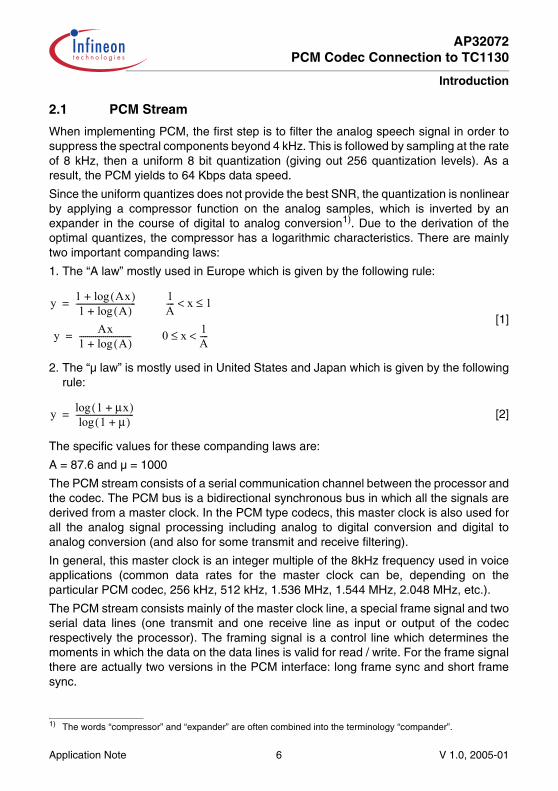
2.1 PCM Stream
When implementing PCM, the first step is to filter the analog speech signal in order to suppress the spectral components beyond 4 kHz. This is followed by sampling at the rate of 8 kHz, then a uniform 8 bit quantization (giving out 256 quantization levels). As a result, the PCM yields to 64 Kbps data speed.
Since the uniform quantizes does not provide the best SNR, the quantization is nonlinear by applying a compressor function on the analog samples, which is inverted by an expander in the course of digital to analog conversion1). Due to the derivation of the optimal quantizes, the compressor has a logarithmic characteristics. There are mainly two important companding laws:
1. The “A law” mostly used in Europe which is given by the following rule:
y 1 Ax( )log+1 A( )log+
------------------------------=1A---- x 1≤<
y Ax1 A( )log+--------------------------= 0 x 1
A----<≤[1]
2. The “µ law” is mostly used in United States and Japan which is given by the following rule:
y 1 µx+( )log1 µ+( )log-----------------------------= [2]
The specific values for these companding laws are:
A = 87.6 and µ = 1000
The PCM stream consists of a serial communication channel between the processor and the codec. The PCM bus is a bidirectional synchronous bus in which all the signals are derived from a master clock. In the PCM type codecs, this master clock is also used for all the analog signal processing including analog to digital conversion and digital to analog conversion (and also for some transmit and receive filtering).
In general, this master clock is an integer multiple of the 8kHz frequency used in voice applications (common data rates for the master clock can be, depending on the particular PCM codec, 256 kHz, 512 kHz, 1.536 MHz, 1.544 MHz, 2.048 MHz, etc.).
The PCM stream consists mainly of the master clock line, a special frame signal and two serial data lines (one transmit and one receive line as input or output of the codec respectively the processor). The framing signal is a control line which determines the moments in which the data on the data lines is valid for read / write. For the frame signal there are actually two versions in the PCM interface: long frame sync and short frame sync.
1) The words “compressor” and “expander” are often combined into the terminology “compander”.
Application Note 6 V 1.0, 2005-01

AP32072PCM Codec Connection to TC1130
Introduction
The long frame sync is the industry name for a clocking format that controls the transfer of the PCM data words. This signal, the frame sync is used for two specific synchronizing functions. The first synchronizing function is to synchronize the PCM data word transfer and the second is to control the internal (codec) analog to digital and digital to analog conversions. The term “sync” refers to the function of synchronizing the PCM data word onto or off the multiplexed serial PCM data bus (also known as PCM highway).
The short frame sync has the same functionality as the long frame sync signal but its duration is just a pulse in the beginning of the transmission / receiving frame. In this case the short frame sync signal is used as a “pre-synchronization” that is used to tell the internal logic (of the codec) to clock out the PCM data word under complete control of the data clock.
Note: For this application, only the long frame sync signal is relevant.
For a stereo codec (two channels included on-chip) the frame sync signal will be generated separately for each of the channels (like two independent mono codecs connected on the same PCM bus). Depending on the master clock frequency, the number of voice channels (8 kHz) can vary. For example, in the case of a master clock with a frequency of 2.048 MHz, the number of 8 kHz PCM channels on the PCM highway is 32.
An example of the framing signals together with the data and master clock is shown in Figure 2. In this figure a connection in which the processor is the master, that is it generates all the needed signals to operate the codec is described.
1 2 3 4 5 6 7 8
1 2 3 4 5 6 7 8
MCLK
FS1
FS2
DX
DR
Sampling moments
1 2 3 4 5
1 2 3 4 5
Figure 2 The PCM main timing diagram.
In this example, the data to and from the codec is sampled on the falling edge of the master clock in the system (MCLK). There are two independent channels with separate frame sync signals (FS1 respectively FS2).
Application Note 7 V 1.0, 2005-01

AP32072PCM Codec Connection to TC1130
Introduction
The codec is reading (and also outputting) each sample in the same manner on the PCM bus that is during the assertion of the long frame sync signal. It is up the host processor to put (and retrieve) the samples to (from) the PCM bus during this interval.
The main frequency of the PCM bus can also vary but it will always be in an integer ratio with the 8kHz sampling rate (the codec usually is extracting his internal timing for all operations from this master clock).
As a practical example, the connection between the TC1130 and the MC145481 codec will be presented.
32 slots - 125µs (8kHz)
3.9 µs 30 slots x 3.9 µs
488 ns (2.048 MHz)
CLK
S1
S2
S3
Figure 3 Typical stereo (2 channels) PCM connection.
2.2 SSC Features
The SSC of the TC1130 has the following features that make it appropriate to communicate to an external CODEC in SPI modus:
– Eight Chip Select Outputs– 2 to 16 bits programmable message length– Transfer starts with MSB or LSB first– shifting out on the rising or falling edge– back-to-back transmit capability
In this application the SSC is used in the master mode. It means that the SSC generates both the serial clock and the CS signal, and has to takes care of the communication protocol, baudrate and the interplay between CS signal and SCLK signal. The SSC SCLK output has the property to drive an external clock only when at least one Chip Select is activated. On the other hand, many external CODECs needs continuous serial clock. In order to implement this requirement, SSC needs to communicate one word to the targeted Chip Select, and 31 words to a dummy Chip Select. In this way the SCLK
Application Note 8 V 1.0, 2005-01

AP32072PCM Codec Connection to TC1130
Introduction
is always continuously on. The Chip Select configuration registers SSOC and SSOTC are shadowed. This means, while an ongoing transaction is taking place, the configuration for the next transaction can be prepared. This configuration becomes relevant automatically with the start of the next transaction.
The transmit-buffer/FIFO makes it possible to have back to back transactions without loosing any clock cycles between words. Although the SSC module has a FIFO, its depth is not used in this application
Note: The maximum shift clock frequency for an SSC module in a master mode is fSYS / 2.
.
InvalidInvalid
SSC_APP
SLSOn
MTSR 1.BitLastBit
Slave Select Output Period
tSCLK
Data Frame
Note: This timing example is based on the following setup: CON.PH = CON.PO = 1
MRST
SCLK
1.Bit LastBit
Sample points
1.Bit
Figure 2-1 SSC Operation Overview
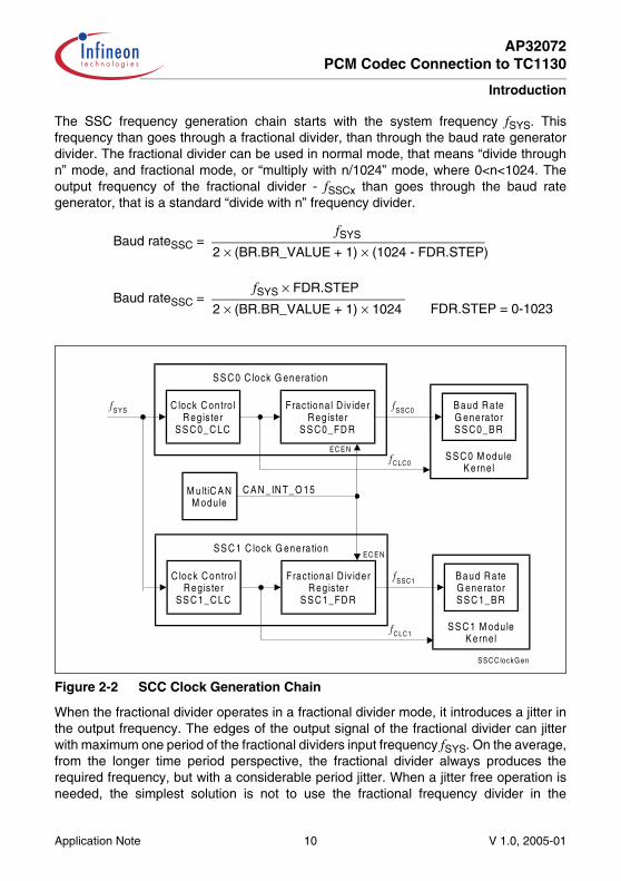
2.3 The Clock Generation
Audio application normally requires precise clock. For example, in order to work exactly with the frequency of 2.048MHz, it is needed that the PLL generates a frequency that is a whole number multiple of 2.048 MHz. Going backwards, the oscillator crystal should be chosen in such a way, that when multiplied with the PLL factor, the before-mentioned requirement of creating the multiple of 2.048MHz is satisfied.
Application Note 9 V 1.0, 2005-01
AP32072PCM Codec Connection to TC1130
Introduction
The SSC frequency generation chain starts with the system frequency fSYS. This frequency than goes through a fractional divider, than through the baud rate generator divider. The fractional divider can be used in normal mode, that means “divide through n” mode, and fractional mode, or “multiply with n/1024” mode, where 0<n<1024. The output frequency of the fractional divider - fSSCx than goes through the baud rate generator, that is a standard “divide with n” frequency divider.
Baud rateSSC =2 × (BR.BR_VALUE + 1) × (1024 - FDR.STEP)
fSYS
Baud rateSSC =2 × (BR.BR_VALUE + 1) × 1024
fSYS × FDR.STEP
FDR.STEP = 0-1023
SSC C lockG en
C lock C ontro lR eg is ter
SS C 0_C LC
fC LC 0
S S C 0 C lock G enera tion
fS S C 0fSYS Frac tiona l D iv iderR eg iste r
S S C 0_FD R
C lock C ontro lR eg is ter
SS C 1_C LC
fC LC 1
S S C 1 C lock G enera tion
fS S C 1Frac tiona l D iv iderR eg iste r
S S C 1_FD R
S S C 0 M odu leK ernel
B aud R ateG eneratorS S C 0_B R
S S C 1 M odu leK ernel
B aud R ateG eneratorS S C 1_B R
M ultiC A NM odule
C A N _IN T_O 15
EC EN
EC EN
Figure 2-2 SCC Clock Generation Chain
When the fractional divider operates in a fractional divider mode, it introduces a jitter in the output frequency. The edges of the output signal of the fractional divider can jitter with maximum one period of the fractional dividers input frequency fSYS. On the average, from the longer time period perspective, the fractional divider always produces the required frequency, but with a considerable period jitter. When a jitter free operation is needed, the simplest solution is not to use the fractional frequency divider in the
Application Note 10 V 1.0, 2005-01

AP32072PCM Codec Connection to TC1130
Introduction
fractional divider mode. On the ot.her hand, when the complete divisor is a relatively big number, then the frequency jitter relative error is in a single digit percent range. The operation of the SSC will not be affected by this jitter, because it is a synchronous interface that drives out its own clock, but if the sampling frequency of the codec depends on this SSC frequency, then some additional noise will be introduced
Application Note 11 V 1.0, 2005-01

AP32072PCM Codec Connection to TC1130
HW Description
3 HW Description
3.1 General
The hardware interfacing of the TC1130 to an external PCM codec was limited due to price considerations. The idea is to provide a connection without any external component between the TC1130 and the PCM codec.
In order to provide an efficient mean of interfacing the PCM device to the TC1130, the Serial Synchronous Channel (SSC) of the microcontroller was chosen. The operation of the synchronous interface is to provide the shifting clock only during data transfers on the data lines (one input and one output). On the other side, the PCM codec needs a continuos clock input at its clock input pin in order to generate the internal signals needed for conversion. For the codec chip, this clock acts as a master clock from which all internal timings are derived (there is no other clock for the codec chip).
This application note demonstrates how to program the SSC of the TC1130 to provide a continuos clock signal by enabling different chip selects signals in different moments of time. The core of the solution is the usage of the slave select lines built-in the SSC interface to select the codec chip during the data transfers and to select a dummy device from / to which to transfer dummy words during the time in which the intended codec is not selected. By using this dummy device, the SSC interface will continue to generate clock (for shifting) and therefore the PCM clock is permanent. The PCM codec chip can use this now continuos clock for its internal timing and operation.
In the case of a stereo codec (or in the case of two chips usage) there will be three such channels: two channels (each with a slave select line for the chip / channel selection) for real audio data (input / output) and one dummy channel used for generating the permanent clock.
Application Note 12 V 1.0, 2005-01

AP32072PCM Codec Connection to TC1130
HW Description
FS
CKDinDout
FS
CKDinDout
SCKDout
Din
SLSO0SLSO1SLSO2
TC1130
SLSO0
SLSO1
SLSO2
Enable
Enable
Enable
SCK
Figure 4 Multiplexing Slave Select Signals
3.2 Connection Example
In this paragraph, a typical connection between the MC145481 PCM codec and the Serial Synchronous Channel of the TC1130 is described.
The connection is using the SSC (Serial Synchronous Channel) of the TC1130 to directly interface the MC145481 codec. For the codec, the framing signal of the receive line and for the transmit line are connected together. This enables the codec to transmit and receive in the same time (full duplex operation) which is supported by the serial interface of the TC1130. The bit clock (BLCK) and master clock (MCLK) are connected also together for the codec chip thus providing the master clock (clock from which all the internal timings are derived for the analog - digital conversions) with the same frequency as the bit symbol clock.
The PCMIN and PCMOUT of the codec chip are connected to the data I/O of the SSC module on the TC1130 side.
In this example, the TC1130 is configured as master i.e. it will generate the clock for the PCM bus. This PCM clock is in fact the serial bit clock for the data shifting of the SSC.
Application Note 13 V 1.0, 2005-01

AP32072PCM Codec Connection to TC1130
HW Description
20
19
18
17
16
15
14
13
12
11
1
2
3
4
5
6
7
8
9
10
VAGRef
RO-
PI
PO-
PO+
VDD
FSR
DR
BCLKR
___PDI
VAG
TI+
TI-
TG
Mu/A
VSS
FST
DT
BCLKT
MCLK
10 kΩ 0.01 µF
10 kΩ 1.0 µF
10 kΩ 10 kΩ
1.0 µF+3 V
ANALOG IN
8 kHz
PCM OUT
2.048 MHz
0.1 µF
20 kΩAUDIO OUTRL> 2 kΩ
20 kΩ68 µF+
10 kΩ
AUDIO OUTRL> 150 Ω
0.1 µF
+3 V
PCM IN
TC1130
SLx
MRST
MTSR
SSC CK
Slave Select
Master Rx Slave Tx
Master Tx Slave Rx
SSC Clock
SSC
1, 2
Figure 5 Typical connection of the MC145481 codec to the TC1130
Application Note 14 V 1.0, 2005-01
AP32072PCM Codec Connection to TC1130
SW Description
4 SW DescriptionTo connect a PCM codec to the TC1130, the Serial Synchronous Channel peripheral is used (SSC). This peripheral is not meant for connecting a PCM codec and some extra software must be added to it to handle this type of connection. In this case the internal TC1130 DMA controller is used to be able to support the timing constraints of a PCM stream.
This chapter explains how the SSC and DMA peripherals are configured for PCM operation and shows a practical implementation of it.
4.1 SW Architecture
4.1.1 Clock Generation
A PCM stream is very similar to a synchronous data transmission that you can find on most microcontrollers.
The main difference here which we have to carefully take care about is the fact that the clock signal which is used to shift data in and out must be constant. This means that the clock must never stop running (refer to chapter 1 for more details).
In a synchronous communication channel, the clock is running only when data is transmitted, therefore we need a way to create this clock continuously.
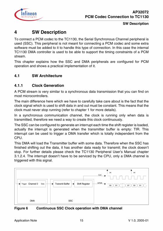
The SSC can be configured to generate an interrupt each time the shift register is loaded, actually the interrupt is generated when the transmitter buffer is empty: TIR. This interrupt can be used to trigger a DMA transfer which is totally independent from the CPU.
This DMA will load the Transmitter buffer with some data. Therefore when the SSC has finished shifting out the data, it has another data ready for transmit; the clock doesn’t stop. For further details please check the TC1130 Peripheral User’s Manual chapter 3.1.2.4. The interrupt doesn’t have to be serviced by the CPU, only a DMA channel is triggered with this signal.
Transmit Buffer
SSC
MTSR
CLK
D0 D1 ... D7 D0 D1 ...
DMA
Channel 0
int int
Trigger Dest. Shift Register
Figure 6 Continuous SSC Clock operation with DMA channel
Application Note 15 V 1.0, 2005-01

AP32072PCM Codec Connection to TC1130
SW Description
Most of PCM codecs need this clock for internal operation. The audio signal (coming from the DAC) is based on this frequency which should be 2.048 MHz. The shift baudrate should therefore be 2.048 MBauds.
The TC1130 has very flexible clock and baudrate generation facilities. However this 2.048MHz clock cannot be derived from any input clock.
The internal baudrate is defined by:
( ) ( )FDRBRfBaudrate SYS
SSC −⋅+⋅=
102412
With:
BR: Value for baudrate timer (16 bits value)
FDR: Fractional divider reload value
Fsys: System clock frequency
There is a limitation here if you want to generate a 2.048MHz. If you use a crystal (i.e. 20MHz) for CPU operation at 150MHz, then you will get:
( ) ( ) 31055.1840967500010241 ==−⋅+ FDRBR
As BR and FDR are integer number, this is impossible to realize.
The crystal should therefore be selected to suit the needs.
Here we selected a 12.288 MHz crystal with which you can easily derive a 2.048 MHz clock:
BR = 17 = 0x0011
FDR = 0 = 0x0000
The CPU frequency is chosen to be 147.456 MHz (this is not described here as this is not the purpose of this appnote), i.e. PLL is setup to multiply by 12 and the system frequency (fsys) is equal to half of the CPU frequency (the FPI bus maximum frequency is 100 MHz).
4.1.2 Data output
As seen before, a PCM codec needs a 2.048 MHz clock. The data output rate is then 8 kHz which is the audio quality. Internally the codec uses this clock and divides it by 256 (2048/256 = 8).
Application Note 16 V 1.0, 2005-01

AP32072PCM Codec Connection to TC1130
SW Description
The data has to be written to the codec with an 8 kHz rate.
Using the DMA, data is written every 2048/8 = 256 kHz (assuming 8 bits data). Therefore the interesting data has to be written every 32 words.
The DMA source is configured to be a 32 words circular buffer. The data to be transmitted to the codec is chosen for example to be located at index 0 for the left channel and at index 1 for the right channel.
The DMA channel 0 is setup to generate an interrupt when it reaches position 15. This interrupt is used by the higher level software (i.e. the device driver) to update the data for next sample. In this interrupt, the input sample is also read; this will be described later on.
Transmit/Receive
Shift Register
Transmit Buffer
SSC
MTSR
CLK
Left
DMA
Channel 0
int
0 0 0 0 0 0
0 1 2 3 28 29 30 31index
Transmit SlotsDataLeft
Trigger
SourceDest.
32 words (32 bits wide) circular buffer
0 14 15 16 01 3131 1
8 clocks
Interrupt to CPU
DataRight
Right Left Right
Figure 7 Constant 8 kHz data throughput
On this picture you can see the 32 words circular buffer. This buffer uses 32 bits wide words as the SSC transmit buffer is a 32 bits register. Only the 8 LSB bits are relevant in this case.
4.1.3 Chip Select Generation
Using the configuration above, we see that the data is sent out every 8 kHz. We need now a way to tell the PCM Codec that the data during this time is relevant and for 30/32 of the time irrelevant. This is done using Chip Select (or Frame Start) on the Codec.
The TC1130 SSC has the possibility to generate Slave Select Outputs. You can have a maximum of 8 per SSC. The outputs are controlled with a specific register which is buffered the same way as the Transmit buffer. This means that if you write something to this register, the Slave Select Outputs will be modified on the next start of transmission. Therefore you can really set those pins when you want them to be. This is further detailed in the Peripheral User's Manual chapter 3.1.2.11.
Application Note 17 V 1.0, 2005-01

AP32072PCM Codec Connection to TC1130
SW Description
So to say to the Codec that the information is relevant for slots 0 and 1, we need to set the Slave Select Output register for those periods. We can use for this another DMA Channel which has this register as destination.
The source of this channel is just using the same structure with a 32 words circular buffer.
Note: Depending on your codec and the way you connect it to the Slave Select Outputs; you will need to set the values differently.
The Trigger used for this channel is of course the same as Channel 0, every time a word has been loaded in the transmit shift register.
The Channel selected here is Channel 3. This is due to the fact that TIR signal which should trigger the DMA can only be connected to Channel 0 or 3. For more details please refer to the System User's manual chapter 17.3.1.1 and 4.6.
• Example using 2 separated codecs for each left and right channel:
Here the Left channel codec is connected to SLSO1 and the Right channel to SLSO2. 00FF: SLSO[2..1]=’00’; 02FF: SLSO[2..1]=’10’; 04FF: SLSO[2..1]=’01’
Note: This was chosen because those signals are located on the same connector on the Triboard but any Slave Select Output could have been chosen.
MTSR
CLK
Left
int
0 0 0 0 0 0
0 1 2 3 28 29 30 31index
Transmit SlotsDataLeft
32 words (32 bits wide) circular buffer
0 14 15 16 01 3131 1
8 clocks Interrupt to CPU
DataRight
Right Left Right
FF FF FF FF FF FF
0 1 2 3 28 29 30 31index
Control Slots02FF 04FF
Transmit Buffer
SSCDMA
Channel 0Trigger
SourceDest.
Slave SelectOutputs
Generation
Slave SelectOutput RegisterChannel 3
Trigger
SourceDest.
Transmit/Receive
Shift Register
SLSO1
SLSO2
Figure 8 Chip Select Generation for 2 codecs configuration
• Example using a single stereo codec:
Here the codec has a chip select connected to SLSO1 and a pin to indicate Left or Right channel connected to SLSO2
00FF: SLSO[2..1]=’00’; 02FF: SLSO[2..1]=’10’; 06FF: SLSO[2..1]=’11’
Application Note 18 V 1.0, 2005-01

AP32072PCM Codec Connection to TC1130
SW Description
Transmit Buffer
SSC
MTSR
CLK
Left
DMA
Channel 0
int
0 0 0 0 0 0
0 1 2 3 28 29 30 31index
Transmit SlotsDataLeft
Trigger
SourceDest.
32 words (32 bits wide) circular buffer
0 14 15 16 01 3131 1
8 clocks Interrupt to CPU
DataRight
Right Left Right
FF FF FF FF FF FF
0 1 2 3 28 29 30 31index
Control Slots02FF 06FF
Slave SelectOutputs
Generation
Slave SelectOutput RegisterChannel 3
Trigger
SourceDest.
SLSO1
SLSO2
Transmit/Receive
Shift Register
Figure 9 Chip Select Generation for Stereo codec
4.1.4 Input Handling
Of course we want to be able to read from the codec as well. The TC1130 can work in a full-duplex mode allowing output samples to be written to the codec and incoming samples to be read from it at the same time.
In full-duplex mode, the receiver shift register is shifted at the same time as the transmit shift register. This means that when sending out Left Channel for example, the receive shift register is also shifted and the Left incoming Channel data will then be valid on the next slot.
To receive the data we use another DMA Channel which is this time triggered when data has been received in the receive shift register. Once the data has been received, the DMA is triggered and saves the value into a third 32 words circular buffer.
The Channel selected here is Channel 1. This is due to the fact that RIR signal which should trigger the DMA can only be connected to Channel 1 or 4. For more details please refer to the System User's manual chapter 17.3.1.1 and 4.6.
As explained before, the left channel will be received in slot 1 and the right channel in slot 2.
Note: Of course you could setup Channel 1 to start with one step behind Channel 0 and 3. In this case you will have all samples on the same slots (i.e. Left on Slot 0, Right on Slot 1). This is just a software issue.
Application Note 19 V 1.0, 2005-01

AP32072PCM Codec Connection to TC1130
SW Description
The example shown here is using the 2 codec configuration:
Channel 1
Transmit/Receive
Shift Register
Transmit Buffer
SSC
MTSR
CLK
Left
DMA
Channel 0
int
0 0 0 0 0 0
0 1 2 3 28 29 30 31index
Transmit SlotsDataLeft
Trigger
SourceDest.
32 words (32 bits wide) circular buffer
0 15 16 01 3131 1
8 clocks Interrupt to CPU
DataRight
Right Left Right
FF FF FF FF FF FF
0 1 2 3 28 29 30 31index
Control Slots02FF 04FF
Slave SelectOutputs
Generation
Slave SelectOutput RegisterChannel 3
Trigger
SourceDest.
SLSO1
SLSO2
? ? ? ? ?
0 1 2 3 28 29 30 31index
Receive Slots? LeftData
RightData
Receive BufferTrigger
Dest.Source MRST
Left
1 31 12 00 2
Right Left Right
2
1615
int
Figure 10 Chip Select Generation for Stereo codec
Application Note 20 V 1.0, 2005-01

AP32072PCM Codec Connection to TC1130
SW Description
4.2 SW Implementation
The software implementation for PCM Codec support on TC1130 is fairly simple and has basically only peripheral initialization. The only running software part will be an interrupt which comes every time a new sample has been sent (and one received as well). This makes this implementation very light for the CPU.
As a matter of fact if there would be a real PCM Codec interface in TC1130, the CPU load would be the same as you would receive the same interrupt when something has been sent out.
Here the load will not be on the CPU side but on the FPI bus side. Indeed, you need each time a word was sent out, to reload the Slave Select Output and Transmit Buffer registers. This is done using DMA which means that it needs to get access to the FPI0 bus and especially EBU (as the data might be in external memory) for 2 bus cycles (and more if the data is data is in SDRAM). Then DMA will get access to FPI1 bus to put data in the SSC registers. For more details about FPI busses and DMA please refer to the System User’s Manual chapter 17.1.5 and 18.4.
You also need another FPI0 bus cycle to write the received data back to the memory. In total the FPI0 bus is used for 3 bus cycles (here cycle means a read or a write, this could be more than one CPU cycle).
For all configuration, the CPU is assumed to be running at 147.456 MHz with an external 12.288 Mhz crystal. The FPI bus and peripherals running at half the CPU frequency, 73.728 MHz.
4.2.1 Configuration
The SSC needs to be configured as follow:
– Using normal clock divider, setup for 73.728 MHz internal module clock– Master mode– 8 bits operation with LSB first (depends on codec)– Leading clock edge set to low-to-high transition and shift data on leading edge
(depends on codec)– receive and transmit FIFOs disabled– Baudrate set to 2.048 MBauds– SCLK, MRST, MTSR pins enabled– selected SLSO pins enabled for SSC operation, here SLSO1 and SLSO2.– SLSO pins configured for high level active (depends on codec)– SLSO timing set to no additional delay
Application Note 21 V 1.0, 2005-01

AP32072PCM Codec Connection to TC1130
SW Description
The DMA needs to be configured as follow:
– Service Request node 0 enabled– SSC0, EBU and external EBU space Address Ranges enabled– Channel 0 enabled and set to:
– 32 bits wide transfer– Transfer reload set to 32 (0x20)– Number of Moves set to 1– Source address set to Transmit_Slots array– Source buffer is 128 bytes circular, update factor of 1, increment– Destination address set to SSC Transmit Buffer: SSC0_TB– Destination buffer without any address modification– Hardware Transaction enabled and set to SSC0_0 signal which is connected to TIR
(see SCU configuration)– Continuous Operation selected– Transfer Interrupt enabled and generated when TCOUNT reaches 15 (Transfer
Count Threshold Limit, IRDV)– Channel 3 enabled and set to:
– 32 bits wide transfer– Transfer reload set to 32 (0x20)– Number of Moves set to 1– Source address set to Control_Slots array– Source buffer is 128 bytes circular, update factor of 1, increment– Destination address set to SSC Transmit Buffer: SSC0_SSOC– Destination buffer without any address modification– Hardware Transaction enabled and set to SSC0_0 signal which is connected to TIR
(see SCU configuration)– Continuous Operation selected– Transfer Interrupt disabled
– Channel 1 enabled and set to:– 32 bits wide transfer– Transfer reload set to 32 (0x20)– Number of Moves set to 1– Source address set to SSC Receive Buffer: SSC0_RB– Source buffer without any address modification– Destination address set to Receive_Slots array– Destination buffer is 128 bytes circular, update factor of 1, increment– Hardware Transaction enabled and set to SSC0_1 signal which is connected to RIR
(see SCU configuration)– Continuous Operation selected– Transfer Interrupt disabled
Application Note 22 V 1.0, 2005-01

AP32072PCM Codec Connection to TC1130
SW Description
The DMA requests inputs for Channel 0, 1 and 3 needs to be connected to SSC0_TIR and SSC0_RIR. This is done using a multiplexor which is configured in the System Control Unit (SCU). Please refer to the System User’s Manual chapter 4.6 for more details.
The SCU needs to be configured as follow:
– SSC0_0 DMA request signal connected to TIR: SEL6 set to 0 (in SCU_DMARS)– SSC0_1 DMA request signal connected to RIR: SEL7 set to 1
Note: The logic implemented in the DMA controller to support circular buffer uses a mask approach. This means that the buffers must be aligned to boundaries. In this case for 128 bytes buffers, they must be aligned to 128 bytes boundaries.
Commonly, compilers provide a way to align data variables but this is often limited to 32 bytes boundaries. To be able to align it to 128 bytes boundary, it is needed to locate the Slots arrays in specific user-defined sections. In this example, an extra memory segment is defined to locate the Slots arrays.
Once the peripherals are configured, you need to initialize the Slots arrays. The most important one is the Control_Slots array. Please refer to previous diagrams for examples on how to initialize the array.
Nothing else needs to be added except your own specific handling code in the DMA service request node 0.
For demo purposes, you can easily create a loopback using these lines in the request node:
Transmit_Slots[0] = Receive_Slots[1];Transmit_Slots[1] = Receive_Slots[2];
4.2.2 Implementation using Dave
Everything needed to support PCM codec is available directly with Dave. Very few lines of code need to be added by yourself to make it work. Here a step by step approach is shown.
Note: Here the GNU Toolchain and the Red Hat Source Navigator developing environment is used.
Configuring Project Settings:
– In General Tab:– Set Compiler to GNU Settings
Application Note 23 V 1.0, 2005-01

AP32072PCM Codec Connection to TC1130
SW Description
Figure 11 Project Settings: General Tab
Application Note 24 V 1.0, 2005-01

AP32072PCM Codec Connection to TC1130
SW Description
– In System Clock Tab:– Set External Crystal Frequency to 12.288 MHz (depends on your application, you
will need to adapt other settings if you choose a different crystal)– Set PDIV to 2– Set NDIV to 96– Set KDIV to 4– Set VCO Range to 500-600 MHz– Set fcpu/fsys ratio to 2/1
Figure 12 Project Settings: System Clock Tab
Application Note 25 V 1.0, 2005-01

AP32072PCM Codec Connection to TC1130
SW Description
– In Interrupt System Tab:– Enable Interrupts
Figure 13 Project Settings: Interrupt System Tab
Application Note 26 V 1.0, 2005-01

AP32072PCM Codec Connection to TC1130
SW Description
Configuring SSC0:
– In Module Clock Tab:– Enable the SSC Module and select normal clock divider (the module clock should
be by default fsys clock = 73.728 MHz)
Figure 14 SSC0: Module Clock Tab
Application Note 27 V 1.0, 2005-01

AP32072PCM Codec Connection to TC1130
SW Description
– In Pin Selection Tab:– Select Master Mode– Enable MRST0, SCLK0 and MTSR0 pins
Figure 15 SSC0: Pin Selection Tab
Application Note 28 V 1.0, 2005-01

AP32072PCM Codec Connection to TC1130
SW Description
– In Slave Select Pins Tab:– Enable SLSO1 and SLSO2 (you can also use other pins for chip select, however
those are easy as they are located on the same connector on the Triboard)
Figure 16 SSC0: Slave Select Pins Tab
Application Note 29 V 1.0, 2005-01

AP32072PCM Codec Connection to TC1130
SW Description
– In Slave Select Tab:– Set SLSO1 and SLSO2 pins to be High active
Figure 17 SSC0: Slave Select Tab
Application Note 30 V 1.0, 2005-01

AP32072PCM Codec Connection to TC1130
SW Description
– In Baud Rate Tab:– Set the baudrate to 2.048 MBauds (the reload value should be 0x0011)
Figure 18 SSC0: Baud Rate Tab
Application Note 31 V 1.0, 2005-01

AP32072PCM Codec Connection to TC1130
SW Description
– In Functions Tab:– Enable the SSC_vInit and SSC0_vSendData functions
Figure 19 SSC0: Functions Tab
Application Note 32 V 1.0, 2005-01
AP32072PCM Codec Connection to TC1130
SW Description
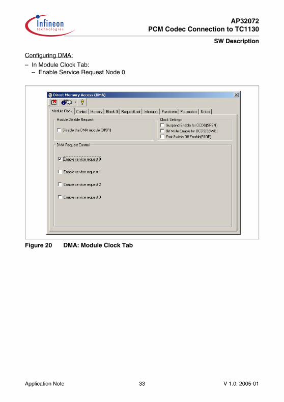
Configuring DMA:
– In Module Clock Tab:– Enable Service Request Node 0
Figure 20 DMA: Module Clock Tab
Application Note 33 V 1.0, 2005-01

AP32072PCM Codec Connection to TC1130
SW Description
– In Memory Tab:– Enable SSC0, EBU, external EBU space Address Ranges
Figure 21 DMA: Memory Tab
Application Note 34 V 1.0, 2005-01

AP32072PCM Codec Connection to TC1130
SW Description
– In Block0 Tab:– Enable Channel 00– Set Transfer Width to 32 bits– Set Transfer Reload Value to 32– Set Continuous Operation– Select Hardware Transaction from Multiplexer Input 2 (this is SSC0_0 signal,
please refer to System User’s Manual chapter 17.3.1.1 for more details)
Figure 22 DMA: Block 0 Tab; DMA Channel 00: General Tab
Application Note 35 V 1.0, 2005-01

AP32072PCM Codec Connection to TC1130
SW Description
– Configure Source Buffer to 128 bytes Circular Buffer– Set Increment Source Buffer Address
Figure 23 DMA: Block 0 Tab; DMA Channel 00: Control Tab
Application Note 36 V 1.0, 2005-01

AP32072PCM Codec Connection to TC1130
SW Description
– Enable Transfer Interrupt when TCOUNT reaches IRDV– Set Transfer Count Threshold Limit to 15
Figure 24 DMA: Block 0 Tab; DMA Channel 00: Interrupt Control Tab
Application Note 37 V 1.0, 2005-01

AP32072PCM Codec Connection to TC1130
SW Description
– Enable Channel 01– Set Transfer Width to 32 bits– Set Transfer Reload Value to 32– Set Continuous Operation– Select Hardware Transaction from Multiplexer Input 3 (this is SSC0_1 signal,
please refer to System User’s Manual chapter 17.3.1.1 for more details)
Figure 25 DMA: Block 0 Tab; DMA Channel 01: General Tab
Application Note 38 V 1.0, 2005-01

AP32072PCM Codec Connection to TC1130
SW Description
– Configure Destination Buffer to 128 bytes Circular Buffer– Set Increment Destination Buffer Address
Figure 26 DMA: Block 0 Tab; DMA Channel 01: Control Tab
Application Note 39 V 1.0, 2005-01

AP32072PCM Codec Connection to TC1130
SW Description
– Enable Channel 03– Set Transfer Width to 32 bits– Set Transfer Reload Value to 32– Set Continuous Operation– Select Hardware Transaction from Multiplexer Input 4 (this is SSC0_0 signal,
please refer to System User’s Manual chapter 17.3.1.1 for more details)
Figure 27 DMA: Block 0 Tab; DMA Channel 03: General Tab
Application Note 40 V 1.0, 2005-01

AP32072PCM Codec Connection to TC1130
SW Description
– Configure Source Buffer to 128 bytes Circular Buffer– Set Increment Source Buffer Address
Figure 28 DMA: Block 0 Tab; DMA Channel 03: Control Tab
Application Note 41 V 1.0, 2005-01

AP32072PCM Codec Connection to TC1130
SW Description
– In Interrupts Tab:– Put the DMA SRN0 Request Node Interrupt on Level 10. This is only an example,
in your system you should make sure that this interrupt is high priority. The maximum latency for this interrupt should be less than 62.5 us (The interrupt is raised on the 15th slot and the value to update is located in the first slot. Therefore at a rate of 8 kHz this is 125 us / 2)
Figure 29 DMA: Interrupts Tab
Application Note 42 V 1.0, 2005-01
AP32072PCM Codec Connection to TC1130
SW Description
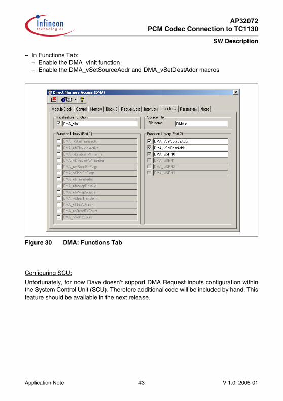
– In Functions Tab:– Enable the DMA_vInit function– Enable the DMA_vSetSourceAddr and DMA_vSetDestAddr macros
Figure 30 DMA: Functions Tab
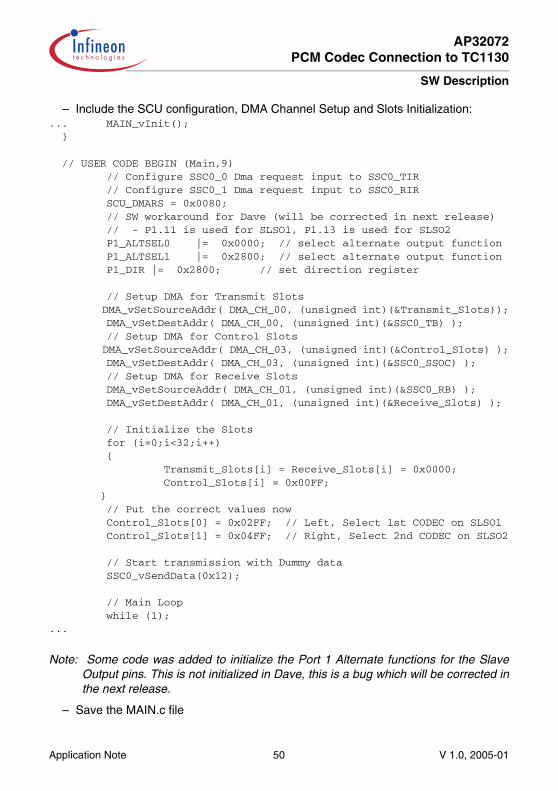
Configuring SCU:
Unfortunately, for now Dave doesn’t support DMA Request inputs configuration within the System Control Unit (SCU). Therefore additional code will be included by hand. This feature should be available in the next release.
Application Note 43 V 1.0, 2005-01

AP32072PCM Codec Connection to TC1130
SW Description
Saving Project, Generating Code and Making a new GNU Project:
– Save your project somewhere on your harddrive.
Note: Please be carefull as we are using the GNU Toolchain, it doesn’t support directory names with spaces inside and this is a valid consideration for the whole path ! i.e. C:\test\TC1130 Projects is not valid, you can use something like C:\test\TC1130_Projects
– You can generate the code by pushing the lightning icon, you should then find those files in your directory: DMA.c, DMA.h, MAIN.c, MAIN.h, SSC0.c, SSC0.h, TC1130Regs.h, Project.dav, Project.dpt and Project.asm
– Copy a target.ld file from the Hightec directory into your project directory, i.e. from C:\Hightec\Tricore\Examples\TriBoard-TC1130\GetStart\target.ld
– You need to edit this file to include an extra segment to put the Slots arrays in. This is because we need to align them to 128 bytes boundaries:
In target.ld file:
You need to include a new memory to put the arrays into:
MEMORY ext_cram (arx!p): org = 0xa0000000, len = 512K ext_dram (aw!xp): org = 0xa0080000, len = 1M ext_dram2 (aw!xp): org = 0xa0180000, len = 384 int_cram (arx!p): org = 0xc0000000, len = 0x8000 int_dram (aw!xp): org = 0xd0000000, len = 0x8000 pcp_data (awp!x): org = 0xf0010000, len = 32K pcp_text (arxp): org = 0xf0020000, len = 16K
The size of the segment is 32*4*3 = 384 bytes.
Then you need to create a section for it (at the very end of the file):
... * Optional sections that may appear regardless of relocating. */ .boffs 0 : KEEP (*(.boffs))
.data2 : *(.data2) > ext_dram2
Application Note 44 V 1.0, 2005-01

AP32072PCM Codec Connection to TC1130
SW Description
– Open the Red Hat Source Navigator– Create a new Project in your project directory where you have generated the files
Figure 31 Source Navigator: Creating a new project
Application Note 45 V 1.0, 2005-01

AP32072PCM Codec Connection to TC1130
SW Description
– Open the Build Settings Dialog: Tools->Build Settings– Create a new Target named debug– Set . as build directory– Select all C files and Add them to the build list
Figure 32 Source Navigator: Build Settings, Source Files
Application Note 46 V 1.0, 2005-01

AP32072PCM Codec Connection to TC1130
SW Description
– In Build Rules, double click on the C rule:– Set Standard Debug– Report All Warnings– Optimization level 2– Tricore v1.3– Select TC1130 as target by including -mcpu=TC1130 as user flag
Note: -mcpu=TC1130 is only valid from Hightec GNU v3.3.5.1 on. If you have an older version you can include -mall-errata instead.
Figure 33 Source Navigator: Build Settings, C Rule
Application Note 47 V 1.0, 2005-01

AP32072PCM Codec Connection to TC1130
SW Description
– In Link Rules:– Change the name of the ouput file to Project.elf– Set Build directory to .– Include Link Script target.ld
Figure 34 Source Navigator: Build Settings, Link Rules
Application Note 48 V 1.0, 2005-01

AP32072PCM Codec Connection to TC1130
SW Description
Adding Code to the Project:
– Close all windows except the Symbols window– Double click on MAIN.c file
– Add the Slots arrays as global variables, you can include it just before the main function and add a variable named i in the main function:
...// USER CODE BEGIN (Main,1)
unsigned int Transmit_Slots[32] __attribute__ ((section (".data2")));unsigned int Control_Slots[32] __attribute__ ((section (".data2")));unsigned int Receive_Slots[32] __attribute__ ((section (".data2")));
// USER CODE END
sword main(void) sword swReturn;
// USER CODE BEGIN (Main,2)
unsigned int i;
// USER CODE END
...
Application Note 49 V 1.0, 2005-01
AP32072PCM Codec Connection to TC1130
SW Description
– Include the SCU configuration, DMA Channel Setup and Slots Initialization:... MAIN_vInit();
// USER CODE BEGIN (Main,9) // Configure SSC0_0 Dma request input to SSC0_TIR // Configure SSC0_1 Dma request input to SSC0_RIR SCU_DMARS = 0x0080; // SW workaround for Dave (will be corrected in next release) // - P1.11 is used for SLSO1, P1.13 is used for SLSO2 P1_ALTSEL0 |= 0x0000; // select alternate output function P1_ALTSEL1 |= 0x2800; // select alternate output function P1_DIR |= 0x2800; // set direction register
// Setup DMA for Transmit Slots DMA_vSetSourceAddr( DMA_CH_00, (unsigned int)(&Transmit_Slots)); DMA_vSetDestAddr( DMA_CH_00, (unsigned int)(&SSC0_TB) ); // Setup DMA for Control Slots DMA_vSetSourceAddr( DMA_CH_03, (unsigned int)(&Control_Slots) ); DMA_vSetDestAddr( DMA_CH_03, (unsigned int)(&SSC0_SSOC) ); // Setup DMA for Receive Slots DMA_vSetSourceAddr( DMA_CH_01, (unsigned int)(&SSC0_RB) ); DMA_vSetDestAddr( DMA_CH_01, (unsigned int)(&Receive_Slots) );
// Initialize the Slots for (i=0;i<32;i++) Transmit_Slots[i] = Receive_Slots[i] = 0x0000; Control_Slots[i] = 0x00FF; // Put the correct values now Control_Slots[0] = 0x02FF; // Left, Select 1st CODEC on SLSO1 Control_Slots[1] = 0x04FF; // Right, Select 2nd CODEC on SLSO2
// Start transmission with Dummy data SSC0_vSendData(0x12);
// Main Loop while (1);...
Note: Some code was added to initialize the Port 1 Alternate functions for the Slave Output pins. This is not initialized in Dave, this is a bug which will be corrected in the next release.
– Save the MAIN.c file
Application Note 50 V 1.0, 2005-01

AP32072PCM Codec Connection to TC1130
SW Description
– Double click on DMA.c file– Add the Loopback code in the DMA Service Request Node, or your own specific
code like a call to the device driver:
...// USER CODE BEGIN (SRN0,1)
extern unsigned int Transmit_Slots[32];extern unsigned int Receive_Slots[32];
// USER CODE END
void DMA_viSRN0(void)
// USER CODE BEGIN (SRN0,2)
if (DMA_INTSR & 0x0001) // is it Channel 0 TCOUNT Match ? // clear the flag DMA_INTCR = 0x0001;
// Loopback incoming samples to output Transmit_Slots[0] = Receive_Slots[1]; Transmit_Slots[1] = Receive_Slots[2];
// USER CODE END
// End of function DMA_viSRN0
...
– Save the DMA.c file
Application Note 51 V 1.0, 2005-01

AP32072PCM Codec Connection to TC1130
SW Description
– In the Symbols window, open the Build dialog: Tools->Build– Select the debug target– Click on Start
Figure 35 Source Navigator: Build, Compiling project
You can download the Project.elf file to the Triboard. You can connect a codec to the SSC0 as described in the previous chapter. If you put audio data (like music or voice) to the codec you should get it on the output.
4.2.3 Results and Measurement
The program was tested using only one codec connected to SLSO1. The input of the codec is connected to the output of a PC playing some music (of course the aim is to interface an audio codec so the result will be a bad quality music). The output of the codec is connected to loudspeakers.
The codec used for this experiment is a MC145481 from Motorola.
On the next picture you can see the clock which is running without any break. The clock is here 2.048 MHz.
Signal 1 is the Frame Select (Chip Select) for the Left Channel codec. You can see it is 8 bits long. Signal 2 is the Frame Select for the Right Channel codec which is not connected here.
Signal 3 is the data which comes out of the SSC and Signal 4 is the data which is shifted out of the Codec.
Application Note 52 V 1.0, 2005-01

AP32072PCM Codec Connection to TC1130
SW Description
Note: According to the test program (loopback), you can check than one frame later, the output is the same as the input data shown here.
Figure 36 Measured Signals: Full Frame
Application Note 53 V 1.0, 2005-01

AP32072PCM Codec Connection to TC1130
SW Description
On this picture you can see more than one frame, you can see that they are coming every 8 kHz.
Note: The noise on the Input signal comes because the line is high-impedance, therefore the logic analyzer is a bit lost.
Figure 37 Measured Signals: Multiple Frames
As you can see, the interface to the Audio PCM Codec is working quite fine without any CPU Load. This is a real advantage.
Also this solution is quite flexible as you can connect a wide variety of codecs, mono, stereo,...
This solution can also be easily adapted to support higher precision codecs using 16 bits data for example. You can also handle more than 1 stereo codec, for example two stereo channels is not a problem; there are a maximum of 8 SLSO pins.
4.2.4 Register summary
In the previous chapter, all initialization code is automatically generated by Dave. This is a very powerful tool. You can extract the value of the registers which it had initialized and use it. In this chapter, all the registers which are needed for this application are listed and the value which should be put in is shown. All registers which are not described here keep their reset value.
A detailed description of each register follows after Table 1.
Application Note 54 V 1.0, 2005-01

AP32072PCM Codec Connection to TC1130
SW Description
Table 1 Register Overview
Register Address Mask Value Comment
SSC0_CLC 0xF0100100 0x00000000 0x00000000 Enable SSC0 Module
SSC0_FDR 0xF010010C 0x00000000 0x000043FF Setup SSC0 Clock to 73.728 MHz
SSC0_BR 0xF0100114 0x00000000 0x00000011 Setup SSC0 Baudrate to 2.048 MBauds
SSC0_CON 0xF0100110 0x00000000 0x00004007 Setup SSC0: 8 bits, LSB first, Rising Edge
SSC0_RXFCON
0xF0100130 0x00000000 0x00000002 Disable SSC0 Receive FIFO
SSC0_TXFCON
0xF0100134 0x00000000 0x00000002 Disable SSC0 Transmit FIFO
SSC0_SSOC
0xF0100118 0x00000000 0x00000006 Use SLSO1 and SLSO2 as Slave Select Outputs. This depends on which pin you connect the codec to.
SSC0_SSOTC
0xF010011C 0x00000000 0x00000000 SLSOx pins use standard timing
SSC0_PISEL
0xF0100104 0x00000000 0x00000000 SSC0 uses MRSTA, MTSRA and SCLKA pins
P1_ALTSEL0
0xF0000D44 0xFFFFD700 0x00000000 Setup P1.13 and P1.11 as Outputs from SSC0 module for SLSO2 and SLSO1
P1_ALTSEL1
0xF0000D48 0xFFFFD700 0x00002800
P1_DIR 0xF0000D18 0xFFFFD700 0x00002800
P2_ALTSEL0
0xF0000E44 0xFFFFFFE7 0x00000018 Setup P2.4 and P2.3 as Outputs from SSC0 module for SCLK0 and MTSR0
P2_ALTSEL1
0xF0000E48 0xFFFFFFE7 0x00000000
P2_DIR 0xF0000E18 0xFFFFFFE7 0x00000018
Application Note 55 V 1.0, 2005-01

AP32072PCM Codec Connection to TC1130
SW Description
DMA_CLC 0xF0003C00 0x00000000 0x00000000 Enable DMA Module
DMA_EER 0xF0003C20 0xFFFFFFFF 0x00000000 Nothing is changed here. Depends on your application
DMA_CHCR00
0xF0003C84 0x00000000 0x00504020 Setup DMA Channel 00 for 32 bits, 1 Move, Triggered by SSC0_0 (TIR)
DMA_CHICR00
0xF0003C88 0x00000000 0x0000F008 Setup to generate an interrupt on Node 0 each time Channel 0 reaches TCOUNT = 15
DMA_SADR00
0xF0003C90 0x00000000 0x???????? Setup DMA Channel 00 Source Address to Transmit_Slots array
DMA_DADR00
0xF0003C94 0x00000000 0xF0100120 Setup DMA Channel 00 Destination Address to SSC0 Transmit Buffer Register
DMA_ADRCR00
0xF0003C8C 0x00000000 0x00000708 Setup DMA Channel 00: Source is 128 bytes circular buffer
DMA_CHCR01
0xF0003CA4 0x00000000 0x00506020 Setup DMA Channel 01 for 32 bits, 1 Move, Triggered by SSC0_1 (RIR)
DMA_CHICR01
0xF0003CA8 0x00000000 0x00000000 DMA Channel 01 doesn't generate any interrupt
DMA_SADR01
0xF0003CB0 0x00000000 0xF0100124 Setup DMA Channel 01 Source Address to SSC0 Receive Buffer Register
DMA_DADR01
0xF0003CB4 0x00000000 0x???????? Setup DMA Channel 01 Destination Address to Receive_Slots array
Table 1 Register Overview
Register Address Mask Value Comment
Application Note 56 V 1.0, 2005-01

AP32072PCM Codec Connection to TC1130
SW Description
DMA_ADRCR01
0xF0003CAC 0x00000000 0x00007080 Setup DMA Channel 01: Destination is 128 bytes circular buffer
DMA_CHCR03
0xF0003CE4 0x00000000 0x00508020 Setup DMA Channel 03 for 32 bits, 1 Move, Triggered by SSC0_0 (TIR)
DMA_CHICR03
0xF0003CE8 0x00000000 0x00000000 DMA Channel 03 doesn't generate any interrupt
DMA_SADR03
0xF0003CF0 0x00000000 0x???????? Setup DMA Channel 03 Source Address to Control_Slots array
DMA_DADR03
0xF0003CF4 0x00000000 0xF0100118 Setup DMA Channel 03 Destination Address to SSC0 Slave Select Control Output Register
DMA_ADRCR03
0xF0003CEC 0x00000000 0x00000708 Setup DMA Channel 03: Source is 128 bytes circular buffer
DMA_ME0PR
0xF0003C3C 0xFFFFFFFF 0x00000000 Pattern detection for DMA not used. Depends on your application
DMA_ME0AENR
0xF0003C44 0xFEBFDFFF 0x01402000 Enable DMA access to EBU and SSC0 module
DMA_ME0ARR
0xF0003C48 0xFF0000FF 0x00FFFF00 Enable DMA access to internal RAM
DMA_HTREQ
0xF0003C1C 0xFFFFFFF4 0x0000000B Enable DMA Hardware Transaction Request for Channel 00, 01 and 03
DMA_SRC0 0xF0003EFC 0x00000000 0x0000100A Enable DMA Service Request Node 00 to priority 10. This depends on your application.
Table 1 Register Overview
Register Address Mask Value Comment
Application Note 57 V 1.0, 2005-01

AP32072PCM Codec Connection to TC1130
SW Description
4.2.5 SSC Registers:
SSC0_CLC [Value: 0000’0000H]SSC0 Clock Control Register [Reset value: 0000’0003H]
31 30 29 28 27 26 25 24 23 22 21 20 19 18 17 16
0
r
15 14 13 12 11 10 9 8 7 6 5 4 3 2 1 0
0 FSOE
SBWE
EDIS
SPEN
DISS
DISR
r rw r rw rw r rw
Field Bits Typ Description
DISR 0 rw Module Disable Request Bit0 Module Enabled
DISS 1 r Module Disable Status Bit
SPEN 2 rw Module Suspend Enable for OCDS0 OCDS Module Enabled
EDIS 3 rw External Request Disable0 External Clock Disable Request Disabled
SBWE 4 w Module Suspend Bit Write Enable for OCDS0 OCDS Module related register unprotected
FSOE 5 rw Fast Switch Off Enable0 Fast Clock Switch Off disabled
0 [31:6] r Reserved; read as 0; should be written with 0
Application Note 58 V 1.0, 2005-01

AP32072PCM Codec Connection to TC1130
SW Description
SSC0_FDR [Value: 0000’43FFH]SSC0 Fractional Divider Register [Reset value: 0000’0000H]
31 30 29 28 27 26 25 24 23 22 21 20 19 18 17 16
DISCLK
ENHW
SUSREQ
SUSACK 0 RESULT
rwh rw rh rh r rh
15 14 13 12 11 10 9 8 7 6 5 4 3 2 1 0
DM SC SM 0 STEP
rw rw rw r rw
Field Bits Typ Description
STEP [9:0] rw Step Value0x3FF FDR=1023 Fractional Clock Divider not used
SM 11 rw Suspend Mode0 Granted Suspend Mode
SC [13:12] rw Suspend Control00
DM [15:14] rw Divider Mode01 Normal Divider Mode
RESULT [25:16] rh Result Value
SUSACK 28 rh Suspend Mode Acknowledge
SUSREQ 29 rh Suspend Mode Request
ENHW 30 rw Enable Hardware Clock Control0 Hardware Control Disabled
DISCLK 31 rwh Disable Clock0 Clock Enabled
0 10, [27:26]
r Reserved; read as 0; should be written with 0
Here the SSC clock is setup for 73.728 MHz.
Application Note 59 V 1.0, 2005-01

AP32072PCM Codec Connection to TC1130
SW Description
SSC0_BR [Value: 0000’0011H]SSC0 Clock Control Register [Reset value: 0000’0000H]
31 30 29 28 27 26 25 24 23 22 21 20 19 18 17 16
0
r
15 14 13 12 11 10 9 8 7 6 5 4 3 2 1 0
BR_VALUE
rw
Field Bits Typ Description
BR_VALUE 0 rw Baud Rate Timer/Reload Register Value0x0011 Baudrate set to 2.048 MBauds
0 [31:16] r Reserved; read as 0; should be written with 0
Application Note 60 V 1.0, 2005-01

AP32072PCM Codec Connection to TC1130
SW Description
SSC0_CON [Value: 0000’4007H]SSC0 Control Register [Reset value: 0000’0000H]
31 30 29 28 27 26 25 24 23 22 21 20 19 18 17 16
0
r
15 14 13 12 11 10 9 8 7 6 5 4 3 2 1 0
EN MS 0 AREN BEN PEN REN TEN LB PO PH HB BM
rw rw r rw rw rw rw rw rw rw rw rw rw rw rw rw
Field Bits Typ Description
BM [3:0] rw Data Width Selection111 8 Bits Width
HB 4 rw Heading Control0 LSB First
PH 5 rw Clock Phase Control0 Shift transmit data on leading edge, latch on
trailing edge
PO 6 rw Clock Polarity Control0 Leading Clock Edge, low-to-high
LB 7 rw Loop Back Control0 Normal Output
TEN 8 rw Transmit Error Enable0 Ignore Transmit Errors
REN 9 rw Receive Error Enable0 Ignore Receive Errors
PEN 10 rw Phase Error Enable0 Ignore Phase Errors
BEN 11 rw Baudrate Error Enable0 Ignore Baudrate Errors
AREN 12 rw Automatic Reset Enable0 No action upon baudrate error
Application Note 61 V 1.0, 2005-01

AP32072PCM Codec Connection to TC1130
SW Description
SSC0_RXFCON [Value: 0000’0002H]SSC0 Receive FIFO Control Register [Reset value: 0000’0100H]
31 30 29 28 27 26 25 24 23 22 21 20 19 18 17 16
0
r
15 14 13 12 11 10 9 8 7 6 5 4 3 2 1 0
0 RXFITL 0RXTMEN
RXFFLU
RXFEN
r rw r rw w rw
Field Bits Typ Description
RXFEN 0 rw Receive FIFO Enable0 FIFO Disable
RXFFLU 1 w Receive FIFO Flush1 FIFO is Flushed
RXTMEN 2 rw Receive FIFO Transparent Mode Enable0 Transparent Mode Disabled
RXFITL [11:8] rw Receive FIFO Interrupt Trigger Level0x0 not used
0 [7:3], [31:12]
r Reserved; read as 0; should be written with 0
MS 14 rw Master Select1 Master Mode
EN 15 rw Enable Bit1 Transmission and Reception enabled
0 [31:16] r Reserved; read as 0; should be written with 0
Field Bits Typ Description
Application Note 62 V 1.0, 2005-01

AP32072PCM Codec Connection to TC1130
SW Description
SSC0_TXFCON [Value: 0000’0002H]SSC0 Transmit FIFO Control Register [Reset value: 0000’0100H]
31 30 29 28 27 26 25 24 23 22 21 20 19 18 17 16
0
r
15 14 13 12 11 10 9 8 7 6 5 4 3 2 1 0
0 TXFITL 0TXTMEN
TXFFLU
TXFEN
r rw r rw w rw
Field Bits Typ Description
RXFEN 0 rw Transmit FIFO Enable0 FIFO Disable
RXFFLU 1 w Transmit FIFO Flush0 FIFO is Flushed
RXTMEN 2 rw Transmit FIFO Transparent Mode Enable0 Transparent Mode Disabled
RXFITL [11:8] rw Transmit FIFO Interrupt Trigger Level0x0 not used
0 [7:3], [31:12]
r Reserved; read as 0; should be written with 0
Application Note 63 V 1.0, 2005-01

AP32072PCM Codec Connection to TC1130
SW Description
SSC0_SSOC [Value: 0000’0006H]SSC0 Slave Select Output Control Register [Reset value: 0000’0000H]
31 30 29 28 27 26 25 24 23 22 21 20 19 18 17 16
0
r
15 14 13 12 11 10 9 8 7 6 5 4 3 2 1 0
OEN7
OEN6
OEN5
OEN4
OEN3
OEN2
OEN1
OEN0
AOL7
AOL6
AOL5
AOL4
AOL3
AOL2
AOL1
AOL0
rw rw rw rw rw rw rw rw rw rw rw rw rw rw rw rw
Field Bits Typ Description
AOLn n rw Active Output Level0x06 SLSO1 and SLSO2 high active
OENn 8+n rw Output n Enable Control0x00 SLSO1 and SLSO2 inactive
0 [31:16] r Reserved; read as 0; should be written with 0
Note: Here SLSO1 and SLSO2 are used. You can use any output you want.
Application Note 64 V 1.0, 2005-01

AP32072PCM Codec Connection to TC1130
SW Description
SSC0_SSOTC [Value: 0000’0000H]SSC0 Slave Select Output Timing Control Register [Reset value: 0000’0000H]
31 30 29 28 27 26 25 24 23 22 21 20 19 18 17 16
0
r
15 14 13 12 11 10 9 8 7 6 5 4 3 2 1 0
0SLSO7
MOD0 INACT TRAIL LEAD
r rw r rw rw rw
Field Bits Typ Description
LEAD [1:0] rw Slave Output Select Leading Delay00 No Delay
TRAIL [3:2] rw Slave Output Select Trailing Delay00 No Delay
INACT [5:4] rw Slave Output Select Inactive Delay00 No Delay
SLSO7MOD 8 rw SLSO7 Delayed Mode Selection0 Normal Mode selected for SLSO7
0 [7:6], [31:9]
r Reserved; read as 0; should be written with 0
Application Note 65 V 1.0, 2005-01

AP32072PCM Codec Connection to TC1130
SW Description
SSC0_PISEL [Value: 0000’0000H]SSC0 Port Input Select Register [Reset value: 0000’0000H]
31 30 29 28 27 26 25 24 23 22 21 20 19 18 17 16
0
r
15 14 13 12 11 10 9 8 7 6 5 4 3 2 1 0
0 STIP 0 SLSIS SCIS SRIS MRIS
r rw r rw rw rw rw
Field Bits Typ Description
MRIS 0 rw Master Mode Receive Input Select0 MSRTA Selected
SRIS 1 r Slave Mode Receive Input Select0 MTSRA Selected
SCIS 2 rw Slave Mode Clock Input Select0 SCLKA Selected
SLSIS [5:3] rw Slave Mode Select Input Selection000 No Input Line Selected
STIP 8 rw Slave Transmit Idle State Polarity0 Not used in Master Mode
0 [7:6], [31:9]
r Reserved; read as 0; should be written with 0
Note: MLI0 on TC1130 has only one pair of pins. Therefore selecting port A or port B has no influence.
Application Note 66 V 1.0, 2005-01

AP32072PCM Codec Connection to TC1130
SW Description
P1_ALTSEL0 [Value: 0000’0000H]Port1 Alternate Select Register 0 [Reset value: 0000’0000H]
31 30 29 28 27 26 25 24 23 22 21 20 19 18 17 16
0
r
15 14 13 12 11 10 9 8 7 6 5 4 3 2 1 0
P15 P14 P13 P12 P11 P10 P9 P8 P7 P6 P5 P4 P3 P2 P1 P0
rw rw rw rw rw rw rw rw rw rw rw rw rw rw rw rw
Field Bits Typ Description
Pn n rw Port 1 Pin n Alternate Output Selection0 Normal GPIO or Alternate Select 2, see next
table for P1_ALTSEL1
0 [31:16] r Reserved; read as 0; should be written with 0
Application Note 67 V 1.0, 2005-01

AP32072PCM Codec Connection to TC1130
SW Description
P1_ALTSEL1 [Value: 0000’2800H]Port1 Alternate Select Register 1 [Reset value: 0000’0000H]
31 30 29 28 27 26 25 24 23 22 21 20 19 18 17 16
0
r
15 14 13 12 11 10 9 8 7 6 5 4 3 2 1 0
P15 P14 P13 P12 P11 P10 P9 P8 P7 P6 P5 P4 P3 P2 P1 P0
rw rw rw rw rw rw rw rw rw rw rw rw rw rw rw rw
Field Bits Typ Description
Pn n rw Port 1 Pin n Alternate Output Selection0 Normal GPIO1 Alternate Select 2
0 [31:16] r Reserved; read as 0; should be written with 0
Here P1.13 and P1.11 are used for SLSO2 and SLSO1 pins. You can choose different SLSO pins to connect your CODEC on.
Application Note 68 V 1.0, 2005-01

AP32072PCM Codec Connection to TC1130
SW Description
P1_DIR [Value: 0000’2800H]Port1 Direction Register [Reset value: 0000’0000H]
31 30 29 28 27 26 25 24 23 22 21 20 19 18 17 16
0
r
15 14 13 12 11 10 9 8 7 6 5 4 3 2 1 0
P15 P14 P13 P12 P11 P10 P9 P8 P7 P6 P5 P4 P3 P2 P1 P0
rw rw rw rw rw rw rw rw rw rw rw rw rw rw rw rw
Field Bits Typ Description
Pn n rw Port 1 Pin n Direction Control0 Input1 Output
0 [31:16] r Reserved; read as 0; should be written with 0
Here P1.13 and P1.11 are used for SLSO2 and SLSO1 pins so they need to be setup as output
Application Note 69 V 1.0, 2005-01

AP32072PCM Codec Connection to TC1130
SW Description
P2_ALTSEL0 [Value: 0000’0018H]Port2 Alternate Select Register 0 [Reset value: 0000’0000H]
31 30 29 28 27 26 25 24 23 22 21 20 19 18 17 16
0
r
15 14 13 12 11 10 9 8 7 6 5 4 3 2 1 0
P15 P14 P13 P12 P11 P10 P9 P8 P7 P6 P5 P4 P3 P2 P1 P0
rw rw rw rw rw rw rw rw rw rw rw rw rw rw rw rw
Field Bits Typ Description
Pn n rw Port 2 Pin n Alternate Output Selection1 Alternate Select 1
0 [31:16] r Reserved; read as 0; should be written with 0
P2.4 and P2.3 are selected as output for SCLK0 and MTSR0.
Application Note 70 V 1.0, 2005-01

AP32072PCM Codec Connection to TC1130
SW Description
P2_ALTSEL1 [Value: 0000’0000H]Port2 Alternate Select Register 1 [Reset value: 0000’0000H]
31 30 29 28 27 26 25 24 23 22 21 20 19 18 17 16
0
r
15 14 13 12 11 10 9 8 7 6 5 4 3 2 1 0
P15 P14 P13 P12 P11 P10 P9 P8 P7 P6 P5 P4 P3 P2 P1 P0
rw rw rw rw rw rw rw rw rw rw rw rw rw rw rw rw
Field Bits Typ Description
Pn n rw Port 2 Pin n Alternate Output Selection0 Normal GPIO or Alternate Select 1, see
previous table for P2_ALTSEL0
0 [31:16] r Reserved; read as 0; should be written with 0
Application Note 71 V 1.0, 2005-01

AP32072PCM Codec Connection to TC1130
SW Description
P2_DIR [Value: 0000’0000H]Port2 Direction Register [Reset value: 0000’0018H]
31 30 29 28 27 26 25 24 23 22 21 20 19 18 17 16
0
r
15 14 13 12 11 10 9 8 7 6 5 4 3 2 1 0
P15 P14 P13 P12 P11 P10 P9 P8 P7 P6 P5 P4 P3 P2 P1 P0
rw rw rw rw rw rw rw rw rw rw rw rw rw rw rw rw
Field Bits Typ Description
Pn n rw Port 2 Pin n Direction Control0 Input1 Output
0 [31:16] r Reserved; read as 0; should be written with 0
Here P2.4 and P2.3 are used for SCLK0 and MTSR0 pins so they need to be setup as output
Application Note 72 V 1.0, 2005-01

AP32072PCM Codec Connection to TC1130
SW Description
4.2.6 DMA Registers:
DMA_CLC [Value: 0000’0000H]DMA Clock Control Register [Reset value: 0000’0000H]
31 30 29 28 27 26 25 24 23 22 21 20 19 18 17 16
0
r
15 14 13 12 11 10 9 8 7 6 5 4 3 2 1 0
0 FSOE
SBWE 0 SP
EN DISS DISR
r rw w rw rw r rw
Field Bits Typ Description
DISR 0 rw Module Disable Request Bit0 Module Enabled
DISS 1 r Module Disable Status Bit
SPEN 2 rw Module Suspend Enable for OCDS0 OCDS Module Enabled
0 3 rw Reserved; returns 0 if read; must be written with 0
SBWE 4 w Module Suspend Bit Write Enable for OCDS0 OCDS Module related register unprotected
FSOE 5 rw Fast Switch Off Enable0 Fast Clock Switch Off disabled
0 [31:6],3
r Reserved; read as 0; should be written with 0
Application Note 73 V 1.0, 2005-01

AP32072PCM Codec Connection to TC1130
SW Description
DMA_EER [Value: 0000’0000H]DMA Enable Error Register [Reset value: 0000’0000H]
31 30 29 28 27 26 25 24 23 22 21 20 19 18 17 16
TRLINP 0 ME0INP 0E
ME0DER
EME0SER
rw r rw r rw rw
15 14 13 12 11 10 9 8 7 6 5 4 3 2 1 0
0E
TRL07
ETRL06
ETRL05
ETRL04
ETRL03
ETRL02
ETRL01
ETRL00
r rw rw rw rw rw rw rw rw
Field Bits Typ Description
ETRL0n(n=0-7)
n rw Enable Transaction Request Lost for DMA Channel 0n0 Request Lost disabled
EME0SER 16 rw Enable Move Engine 0 Source Error0 Interrupt Disabled
EME0DER 17 rw Enable Move Engine 0 Destination Error0 Interrupt Disabled
ME0INP [23:20] w Move Engine 0 Error Interrupt Node Pointer0x0 Errors go to Node 0
TRLINP [31:28] rw Transaction Lost Interrupt Node Pointer0x0 Errors go to Node 0
0 [15:8],[19:18],[27:24]
r Reserved; read as 0; should be written with 0
Application Note 74 V 1.0, 2005-01
AP32072PCM Codec Connection to TC1130
SW Description
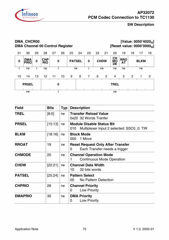
DMA_CHCR00 [Value: 0050’4020H]DMA Channel 00 Control Register [Reset value: 0000’0000H]
31 30 29 28 27 26 25 24 23 22 21 20 19 18 17 16
0 DMAPRIO 0 CHP
RIO 0 PATSEL 0 CHDWCHMODE
RROAT BLKM
r rw r rw r rw r rw rw rw rw
15 14 13 12 11 10 9 8 7 6 5 4 3 2 1 0
PRSEL 0 TREL
rw r rw
Field Bits Typ Description
TREL [8:0] rw Transfer Reload Value0x20 32 Words Tranfer
PRSEL [15:13] rw Module Disable Status Bit010 Multiplexer Input 2 selected: SSC0_0: TIR
BLKM [18:16] rw Block Mode000 1 Move
RROAT 19 rw Reset Request Only After Transfer0 Each Transfer needs a trigger
CHMODE 20 rw Channel Operation Mode1 Continuous Mode Operation
CHDW [22:21] rw Channel Data Width10 32 bits words
PATSEL [25:24] rw Pattern Select00 No Pattern Detection
CHPRIO 28 rw Channel Priority0 Low Priority
DMAPRIO 30 rw DMA Priority0 Low Priority
Application Note 75 V 1.0, 2005-01

AP32072PCM Codec Connection to TC1130
SW Description
DMA_CHICR00 [Value: 0000’F008H]DMA Channel 00 Interrupt Control Register [Reset value: 0000’0000H]
31 30 29 28 27 26 25 24 23 22 21 20 19 18 17 16
0
r
15 14 13 12 11 10 9 8 7 6 5 4 3 2 1 0
IRDV INTP WRPP INTCT WRPDE
WRPSE
rw rw rw rw rw rw
Field Bits Typ Description
WRPSE 0 rw Wrap Source Enable0 Wrap Source Interrupt Disabled
WRPDE 1 rw Wrap Destination Enable0 Wrap Destination Interrupt Disabled
INTCT [3:2] rw Interrupt Control10 Interrupt is generated each time TCOUNT
reaches IRDV
WRPP [7:4] rw Wrap Pointer0x0 Not Used
INTP [11:8] rw Interrupt Pointer0x0 Interrupts go to Interrupt Node 0
IRDV [15:12] rw Interrupt Raise Detect Value0xF Interrupt generated after 15 transfers
0 [31:16] r Reserved; read as 0; should be written with 0
0 [12:9], 23, [27:26], 29, 31
r Reserved; read as 0; should be written with 0
Field Bits Typ Description
Application Note 76 V 1.0, 2005-01

AP32072PCM Codec Connection to TC1130
SW Description
DMA_SADR00 [Value: ????’????H]DMA Channel 00 Source Address Register [Reset value: 0000’0000H]
31 30 29 28 27 26 25 24 23 22 21 20 19 18 17 16
SADR
rw
15 14 13 12 11 10 9 8 7 6 5 4 3 2 1 0
SADR
rwh
Field Bits Typ Description
SADR [31:0] rwh Source Start Address0x???????? Address set to Transmit_Slots address
DMA_DADR00 [Value: F010’0120H]DMA Channel 00 Destination Address Register [Reset value: 0000’0000H]
31 30 29 28 27 26 25 24 23 22 21 20 19 18 17 16
DADR
rwh
15 14 13 12 11 10 9 8 7 6 5 4 3 2 1 0
DADR
rwh
Application Note 77 V 1.0, 2005-01

AP32072PCM Codec Connection to TC1130
SW Description
Field Bits Typ Description
DADR [31:0] rw Destination Start Address0xF0100120 Address set to SSC0 Transmit Buffer
address
DMA_ADRCR00 [Value: 0000’0708H]DMA Channel 00 Address Control Register [Reset value: 0000’0000H]
31 30 29 28 27 26 25 24 23 22 21 20 19 18 17 16
0 SHCT
r rw
15 14 13 12 11 10 9 8 7 6 5 4 3 2 1 0
CBLD CBLS INCD DMF INCS SMF
rw rw rw rw rw rw
Field Bits Typ Description
SMF [2:0] rw Source Modification Factor000 The Update Factor is 1 word (32 bits)
INCS 3 r Increment of Source Address1 The Source Address will be Incremented
DMF [6:4] rw Destination Modification Factor000 Destination Address is not modified, cf. CBLD
INCD 7 rw Increment of Destination Address0 Destination Address is not modified, cf. CBLD
CBLS [11:8] rw Circular Buffer Length Source0x7 Buffer is 128 bytes long
CBLD [15:12] rw Circular Buffer Length Source0x0 The Destination Address is not modified
SHCT [17:16] rw Shadow Control00 Shadow Register is not used
0 [31:18] r Reserved; read as 0; should be written with 0
Application Note 78 V 1.0, 2005-01
AP32072PCM Codec Connection to TC1130
SW Description
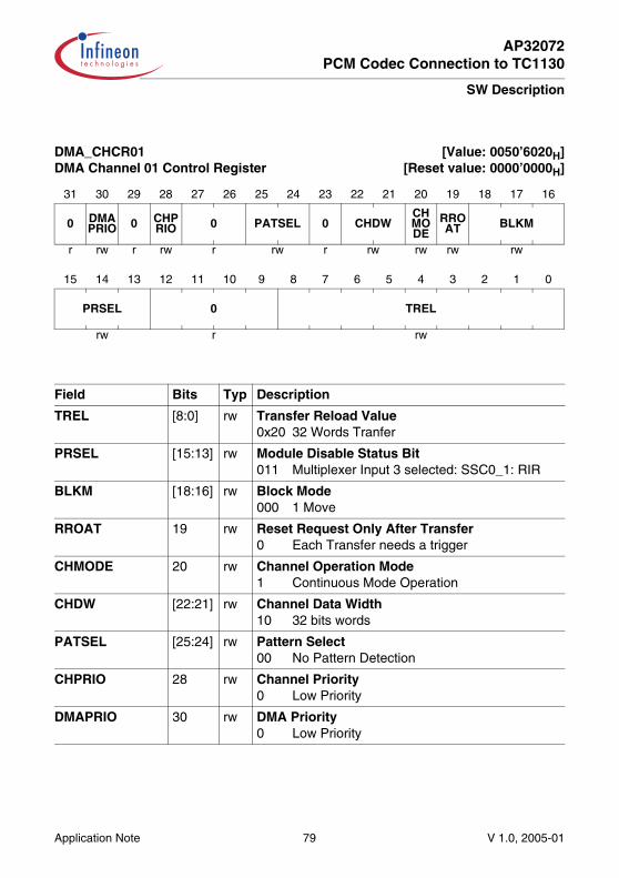
DMA_CHCR01 [Value: 0050’6020H]DMA Channel 01 Control Register [Reset value: 0000’0000H]
31 30 29 28 27 26 25 24 23 22 21 20 19 18 17 16
0 DMAPRIO 0 CHP
RIO 0 PATSEL 0 CHDWCHMODE
RROAT BLKM
r rw r rw r rw r rw rw rw rw
15 14 13 12 11 10 9 8 7 6 5 4 3 2 1 0
PRSEL 0 TREL
rw r rw
Field Bits Typ Description
TREL [8:0] rw Transfer Reload Value0x20 32 Words Tranfer
PRSEL [15:13] rw Module Disable Status Bit011 Multiplexer Input 3 selected: SSC0_1: RIR
BLKM [18:16] rw Block Mode000 1 Move
RROAT 19 rw Reset Request Only After Transfer0 Each Transfer needs a trigger
CHMODE 20 rw Channel Operation Mode1 Continuous Mode Operation
CHDW [22:21] rw Channel Data Width10 32 bits words
PATSEL [25:24] rw Pattern Select00 No Pattern Detection
CHPRIO 28 rw Channel Priority0 Low Priority
DMAPRIO 30 rw DMA Priority0 Low Priority
Application Note 79 V 1.0, 2005-01

AP32072PCM Codec Connection to TC1130
SW Description
DMA_CHICR01 [Value: 0000’0000H]DMA Channel 01 Interrupt Control Register [Reset value: 0000’0000H]
31 30 29 28 27 26 25 24 23 22 21 20 19 18 17 16
0
r
15 14 13 12 11 10 9 8 7 6 5 4 3 2 1 0
IRDV INTP WRPP INTCT WRPDE
WRPSE
rw rw rw rw rw rw
Field Bits Typ Description
WRPSE 0 rw Wrap Source Enable0 Wrap Source Interrupt Disabled
WRPDE 1 rw Wrap Destination Enable0 Wrap Destination Interrupt Disabled
INTCT [3:2] rw Interrupt Control00 No Interrupt is Generated
WRPP [7:4] rw Wrap Pointer0x0 Not Used
INTP [11:8] rw Interrupt Pointer0x0 Not used
IRDV [15:12] rw Interrupt Raise Detect Value0x0 Not used
0 [31:16] r Reserved; read as 0; should be written with 0
0 [12:9], 23, [27:26], 29, 31
r Reserved; read as 0; should be written with 0
Field Bits Typ Description
Application Note 80 V 1.0, 2005-01

AP32072PCM Codec Connection to TC1130
SW Description
DMA_SADR01 [Value: F010’0124H]DMA Channel 01 Source Address Register [Reset value: 0000’0000H]
31 30 29 28 27 26 25 24 23 22 21 20 19 18 17 16
SADR
rw
15 14 13 12 11 10 9 8 7 6 5 4 3 2 1 0
SADR
rwh
Field Bits Typ Description
SADR [31:0] rwh Source Start Address0xF0100124 Address set to SSC0 Receive Buffer
address
DMA_DADR01 [Value: ????’????H]DMA Channel 01 Destination Address Register [Reset value: 0000’0000H]
31 30 29 28 27 26 25 24 23 22 21 20 19 18 17 16
DADR
rwh
15 14 13 12 11 10 9 8 7 6 5 4 3 2 1 0
DADR
rwh
Application Note 81 V 1.0, 2005-01
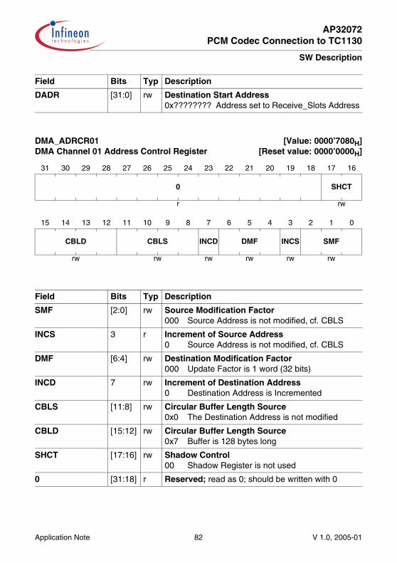
AP32072PCM Codec Connection to TC1130
SW Description
Field Bits Typ Description
DADR [31:0] rw Destination Start Address0x???????? Address set to Receive_Slots Address
DMA_ADRCR01 [Value: 0000’7080H]DMA Channel 01 Address Control Register [Reset value: 0000’0000H]
31 30 29 28 27 26 25 24 23 22 21 20 19 18 17 16
0 SHCT
r rw
15 14 13 12 11 10 9 8 7 6 5 4 3 2 1 0
CBLD CBLS INCD DMF INCS SMF
rw rw rw rw rw rw
Field Bits Typ Description
SMF [2:0] rw Source Modification Factor000 Source Address is not modified, cf. CBLS
INCS 3 r Increment of Source Address0 Source Address is not modified, cf. CBLS
DMF [6:4] rw Destination Modification Factor000 Update Factor is 1 word (32 bits)
INCD 7 rw Increment of Destination Address0 Destination Address is Incremented
CBLS [11:8] rw Circular Buffer Length Source0x0 The Destination Address is not modified
CBLD [15:12] rw Circular Buffer Length Source0x7 Buffer is 128 bytes long
SHCT [17:16] rw Shadow Control00 Shadow Register is not used
0 [31:18] r Reserved; read as 0; should be written with 0
Application Note 82 V 1.0, 2005-01

AP32072PCM Codec Connection to TC1130
SW Description
DMA_CHCR03 [Value: 0050’8020H]DMA Channel 03 Control Register [Reset value: 0000’0000H]
31 30 29 28 27 26 25 24 23 22 21 20 19 18 17 16
0 DMAPRIO 0 CHP
RIO 0 PATSEL 0 CHDWCHMODE
RROAT BLKM
r rw r rw r rw r rw rw rw rw
15 14 13 12 11 10 9 8 7 6 5 4 3 2 1 0
PRSEL 0 TREL
rw r rw
Field Bits Typ Description
TREL [8:0] rw Transfer Reload Value0x20 32 Words Tranfer
PRSEL [15:13] rw Module Disable Status Bit100 Multiplexer Input 4 selected: SSC0_0: TIR
BLKM [18:16] rw Block Mode000 1 Move
RROAT 19 rw Reset Request Only After Transfer0 Each Transfer needs a trigger
CHMODE 20 rw Channel Operation Mode1 Continuous Mode Operation
CHDW [22:21] rw Channel Data Width10 32 bits words
PATSEL [25:24] rw Pattern Select00 No Pattern Detection
CHPRIO 28 rw Channel Priority0 Low Priority
DMAPRIO 30 rw DMA Priority0 Low Priority
Application Note 83 V 1.0, 2005-01
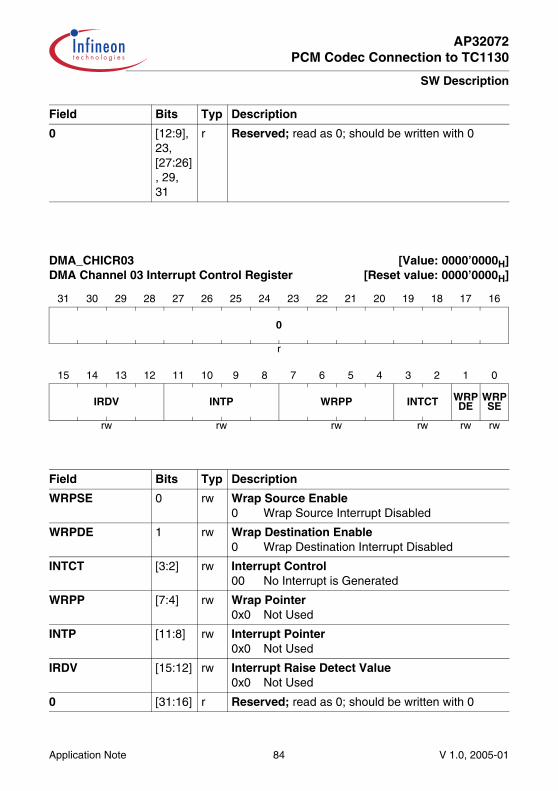
AP32072PCM Codec Connection to TC1130
SW Description
DMA_CHICR03 [Value: 0000’0000H]DMA Channel 03 Interrupt Control Register [Reset value: 0000’0000H]
31 30 29 28 27 26 25 24 23 22 21 20 19 18 17 16
0
r
15 14 13 12 11 10 9 8 7 6 5 4 3 2 1 0
IRDV INTP WRPP INTCT WRPDE
WRPSE
rw rw rw rw rw rw
Field Bits Typ Description
WRPSE 0 rw Wrap Source Enable0 Wrap Source Interrupt Disabled
WRPDE 1 rw Wrap Destination Enable0 Wrap Destination Interrupt Disabled
INTCT [3:2] rw Interrupt Control00 No Interrupt is Generated
WRPP [7:4] rw Wrap Pointer0x0 Not Used
INTP [11:8] rw Interrupt Pointer0x0 Not Used
IRDV [15:12] rw Interrupt Raise Detect Value0x0 Not Used
0 [31:16] r Reserved; read as 0; should be written with 0
0 [12:9], 23, [27:26], 29, 31
r Reserved; read as 0; should be written with 0
Field Bits Typ Description
Application Note 84 V 1.0, 2005-01
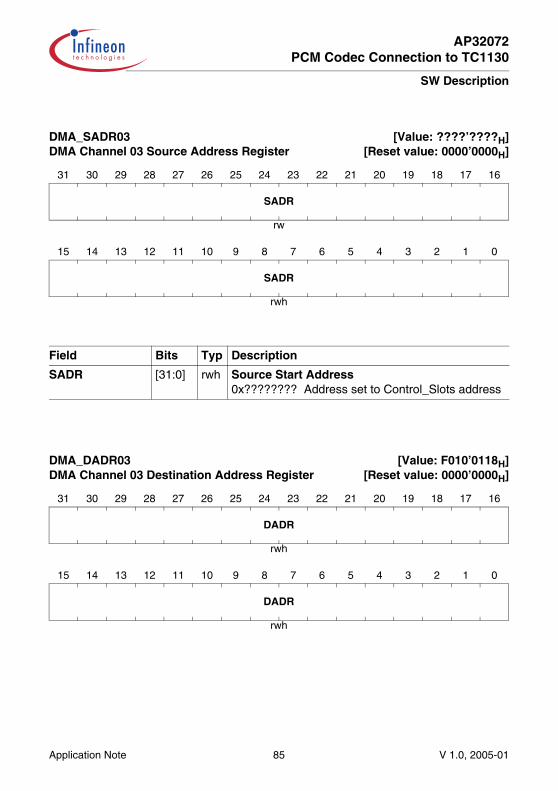
AP32072PCM Codec Connection to TC1130
SW Description
DMA_SADR03 [Value: ????’????H]DMA Channel 03 Source Address Register [Reset value: 0000’0000H]
31 30 29 28 27 26 25 24 23 22 21 20 19 18 17 16
SADR
rw
15 14 13 12 11 10 9 8 7 6 5 4 3 2 1 0
SADR
rwh
Field Bits Typ Description
SADR [31:0] rwh Source Start Address0x???????? Address set to Control_Slots address
DMA_DADR03 [Value: F010’0118H]DMA Channel 03 Destination Address Register [Reset value: 0000’0000H]
31 30 29 28 27 26 25 24 23 22 21 20 19 18 17 16
DADR
rwh
15 14 13 12 11 10 9 8 7 6 5 4 3 2 1 0
DADR
rwh
Application Note 85 V 1.0, 2005-01

AP32072PCM Codec Connection to TC1130
SW Description
Field Bits Typ Description
DADR [31:0] rw Destination Start Address0xF0100118 Address set to SSC0 Slave Select
Control Output (SSOC)
DMA_ADRCR03 [Value: 0000’0708H]DMA Channel 03 Address Control Register [Reset value: 0000’0000H]
31 30 29 28 27 26 25 24 23 22 21 20 19 18 17 16
0 SHCT
r rw
15 14 13 12 11 10 9 8 7 6 5 4 3 2 1 0
CBLD CBLS INCD DMF INCS SMF
rw rw rw rw rw rw
Field Bits Typ Description
SMF [2:0] rw Source Modification Factor000 The Update Factor is 1 word (32 bits)
INCS 3 r Increment of Source Address1 The Source Address will be Incremented
DMF [6:4] rw Destination Modification Factor000 Destination Address is not modified, cf. CBLD
INCD 7 rw Increment of Destination Address0 Destination Address is not modified, cf. CBLD
CBLS [11:8] rw Circular Buffer Length Source0x7 Buffer is 128 bytes long
CBLD [15:12] rw Circular Buffer Length Source0x0 The Destination Address is not modified
SHCT [17:16] rw Shadow Control00 Shadow Register is not used
0 [31:18] r Reserved; read as 0; should be written with 0
Application Note 86 V 1.0, 2005-01
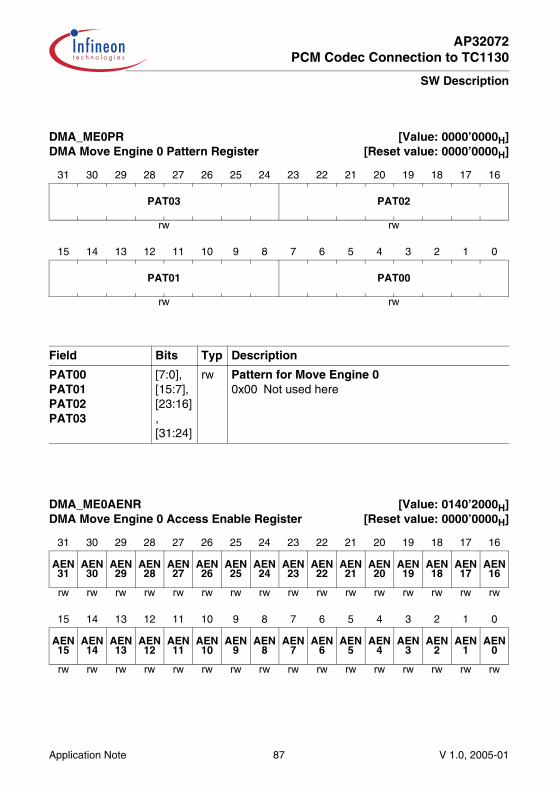
AP32072PCM Codec Connection to TC1130
SW Description
DMA_ME0PR [Value: 0000’0000H]DMA Move Engine 0 Pattern Register [Reset value: 0000’0000H]
31 30 29 28 27 26 25 24 23 22 21 20 19 18 17 16
PAT03 PAT02
rw rw
15 14 13 12 11 10 9 8 7 6 5 4 3 2 1 0
PAT01 PAT00
rw rw
Field Bits Typ Description
PAT00PAT01PAT02PAT03
[7:0], [15:7], [23:16], [31:24]
rw Pattern for Move Engine 00x00 Not used here
DMA_ME0AENR [Value: 0140’2000H]DMA Move Engine 0 Access Enable Register [Reset value: 0000’0000H]
31 30 29 28 27 26 25 24 23 22 21 20 19 18 17 16
AEN31
AEN30
AEN29
AEN28
AEN27
AEN26
AEN25
AEN24
AEN23
AEN22
AEN21
AEN20
AEN19
AEN18
AEN17
AEN16
rw rw rw rw rw rw rw rw rw rw rw rw rw rw rw rw
15 14 13 12 11 10 9 8 7 6 5 4 3 2 1 0
AEN15
AEN14
AEN13
AEN12
AEN11
AEN10
AEN9
AEN8
AEN7
AEN6
AEN5
AEN4
AEN3
AEN2
AEN1
AEN0
rw rw rw rw rw rw rw rw rw rw rw rw rw rw rw rw
Application Note 87 V 1.0, 2005-01

AP32072PCM Codec Connection to TC1130
SW Description
Field Bits Typ Description
AENx x rw Read Enable0x01402000 Enable Read for EBU External Space,
EBU and SSC0 address ranges
Note: For more details refer to Table 17-4 of the System User’s Manual
DMA_ME0ARR [Value: 00FF’FF00H]DMA Move Engine 0 Access Range Register [Reset value: 0000’0000H]
31 30 29 28 27 26 25 24 23 22 21 20 19 18 17 16
SIZE3 SLICE3 SIZE2 SLICE2
rw rw rw rw
15 14 13 12 11 10 9 8 7 6 5 4 3 2 1 0
SIZE1 SLICE1 SIZE0 SLICE0
rw rw rw rw
Field Bits Typ Description
SLICE0,SLICE1,SLICE2,SLICE3
[4:0], [12:8], [20:16], [28:24]
rw Address Slice x (x=0, 1, 2, 3)0x00 Enable access to internal RAM0x1F0x1F0x00
SIZE0,SIZE1,SIZE2,SIZE3
[7:5], [15:13], [23:21], 31:29]
rw Address Size Slice x (x=0, 1, 2, 3)0x00x70x70x0
Note: For more details please refer to chapter 17.3.1.2 of the System User’s Manual.
Application Note 88 V 1.0, 2005-01

AP32072PCM Codec Connection to TC1130
SW Description
DMA_HTREQ [Value: 0000’000BH]DMA Hardware Transaction Request Register [Reset value: 0000’0000H]
31 30 29 28 27 26 25 24 23 22 21 20 19 18 17 16
0 DCH07
DCH06
DCH05
DCH04
DCH03
DCH02
DCH01
DCH00
r w w w w w w w w
15 14 13 12 11 10 9 8 7 6 5 4 3 2 1 0
0 ECH07
ECH06
ECH05
ECH04
ECH03
ECH02
ECH01
ECH00
r w w w w w w w w
Field Bits Typ Description
ECH0n n w Enable Hardware Transfer Request for DMA Channel 0n0x0B Enable Hardware Transaction Request for
Channel 00, 01 and 03
DCH0n n + 16 w Disable Hardware Trasnfer Request for DMA Channel 0n0x00 Don’t disable any Hardware Requests
0 [15:8], [31:24]
r Reserved; read as 0; should be written with 0
Application Note 89 V 1.0, 2005-01

AP32072PCM Codec Connection to TC1130
SW Description
DMA_SRC0 [Value: 0000’100AH]DMA Service Request Control Register 0 [Reset value: 0000’0000H]
31 30 29 28 27 26 25 24 23 22 21 20 19 18 17 16
0
r
15 14 13 12 11 10 9 8 7 6 5 4 3 2 1 0
SETR
CLRR SRR SRE 0 TOS 0 SRPN
w w rh rw r rw r rw
Field Bits Typ Description
SRPN [7:0] rw Service Request Priority Number0x0A Priority set to 0x0A
TOS 10 rw Type Of Service Control0 Priority set to 0x0A
SRE 12 rw Service Request Enable1 Service Request Node Enabled
SRR 13 rh Service Request Flag
CLRR 14 w Request Clear Bit
SETR 15 rw Request Set Bit
0 [9:8], 11, [31:16]
r Reserved; read as 0; should be written with 0
Application Note 90 V 1.0, 2005-01

((91))

h t t p : / / w w w . i n f i n e o n . c o m
Published by Infineon Technologies AG