
SWT - Diagrammatics Lecture 3/4 - Diagramming in OO Software Development - partA 2-May-2000.
Upload
guoxuanchanCategory
view
221download
0
8/10/2019 AP2212-Lecture 9-SWT(1).pdf
http://slidepdf.com/reader/full/ap2212-lecture-9-swt1pdf 1/45
AP2212 – Lecture 9
AC analysis 2
Course organization
TSANG, Stephen
E-mail: [email protected]
Tel: 3442-4618Office: P6706

8/10/2019 AP2212-Lecture 9-SWT(1).pdf
http://slidepdf.com/reader/full/ap2212-lecture-9-swt1pdf 2/45
2
Lecture 08 - Review Managed several examples of circuits with Resistive
(R ), Capacitive (C ) and inductive elements (L).
Reactance (denoted X, units of ohms) is the ratio (magnitude only)
voltage to current: measures how a component opposes the flow of
electricity
X R = R X L = w L X C = 1/w C
Impedance, Z (magnitude and phase) of the current
Z R = R Z L = jw L Z C = - j X C 1 = 1/jw C
t LV d
d I
)(cos t LI v P L w w
Ri v
)(sin t R I v P R w
dt
dV C i
V
QC
)cos( t C
I v
p
C w
w
-

8/10/2019 AP2212-Lecture 9-SWT(1).pdf
http://slidepdf.com/reader/full/ap2212-lecture-9-swt1pdf 3/45
3
Lecture 08 - Review
Graphical
representation ofcomplex impedance
Impedances combine in the
same way as resistors complex impedances can be
Impedance are added , subtracted , multiplied and divided
in the same way as other complex quantities
They can also be expressed in a range of forms such asthe rectangular , polar and exponential forms

8/10/2019 AP2212-Lecture 9-SWT(1).pdf
http://slidepdf.com/reader/full/ap2212-lecture-9-swt1pdf 4/45
4
Power, voltage, and current gains
Power gain is defined as:
Voltage gain is defined as: (why?)
Current gain is defined as: (why?)
Gain =10log P
out
P in
è
ö
ø
÷dB
Gain = 20log V
out
V in
è
ö
ø
÷dB
Gain = 20log I out
I in
è
ö
ø
÷dB
8/10/2019 AP2212-Lecture 9-SWT(1).pdf
http://slidepdf.com/reader/full/ap2212-lecture-9-swt1pdf 5/45
5
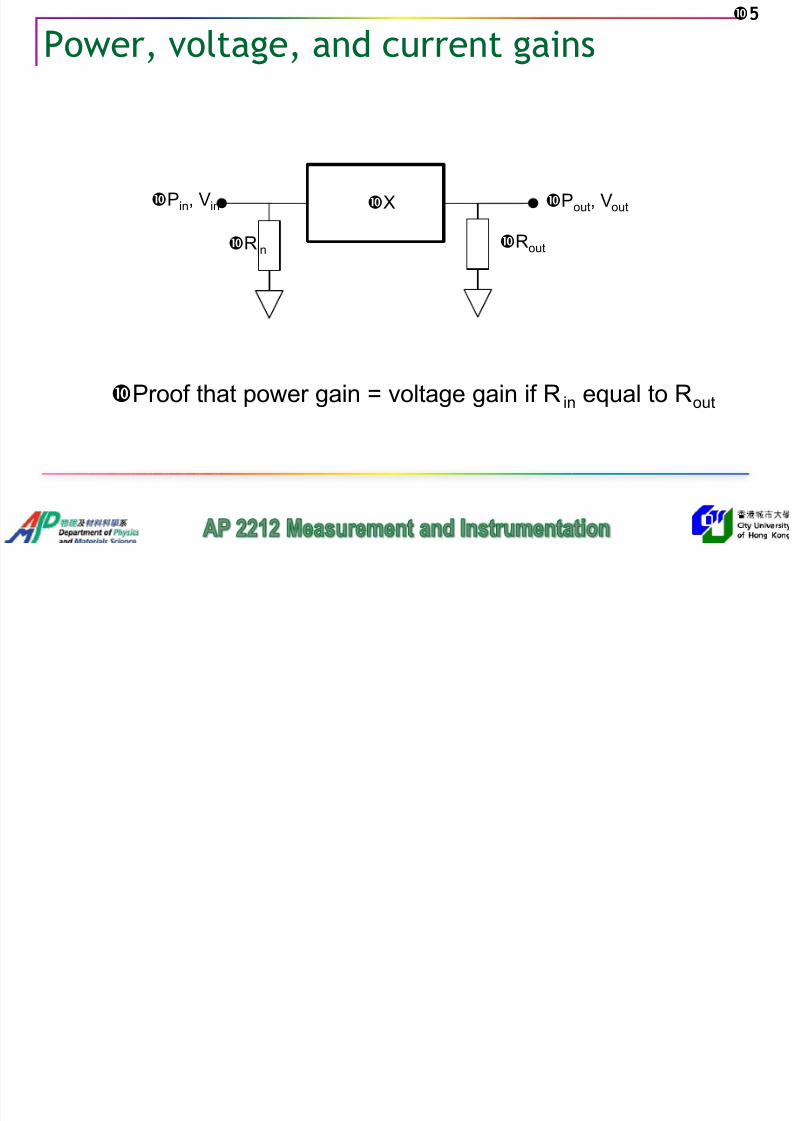
Power, voltage, and current gains
X
RinRout
Pin, Vin Pout, Vout
Proof that power gain = voltage gain if Rin equal to Rout

8/10/2019 AP2212-Lecture 9-SWT(1).pdf
http://slidepdf.com/reader/full/ap2212-lecture-9-swt1pdf 6/45
6
Lecture 09 - Outline
High-pass RC filter
Filter representation
Bode diagram, phasor diagram
Transfer function
Low-pass RL filter
Resonance RLC circuit
Charging and discharging in RCL circuit
Application and engineering manipulation of RCL circuit

8/10/2019 AP2212-Lecture 9-SWT(1).pdf
http://slidepdf.com/reader/full/ap2212-lecture-9-swt1pdf 7/45
7
Application of RCL circuit
Still remember how does a radio works?
Source: National Radio and Astronomy Observatory
1. Convert sound to electrical signal 2. Modulate with carrier frequency
AM
FM
3. Transmit in air4. Received by an antenna
How to extract the sound?
8

8/10/2019 AP2212-Lecture 9-SWT(1).pdf
http://slidepdf.com/reader/full/ap2212-lecture-9-swt1pdf 8/45
8
Application of RCL circuit
FM receiver
FM carrier frequency: 88-108MHz
In human, the audible range of frequency: 20Hzto 20kHz
There are multiple channels in air: e.g. 88.1MHz, 99.7MHz
We have to find a way to select the frequency
A resonance circuit Frequency response
We concern:
The frequency response
The resonance(center) frequency
The width of the spectrum (Bandwidth
The amplification (Gain)
9

8/10/2019 AP2212-Lecture 9-SWT(1).pdf
http://slidepdf.com/reader/full/ap2212-lecture-9-swt1pdf 9/45
9
A High-Pass RC Filter
Consider the following circuit
We want to know what is its function?
?sin:knowweIf output
find
pinput v t V v w
This circuit is commonly
drawn in the following way:
10

8/10/2019 AP2212-Lecture 9-SWT(1).pdf
http://slidepdf.com/reader/full/ap2212-lecture-9-swt1pdf 10/45
10
RC Filter 1/2
vi =V p sin t ® vi =V pe j t
1) Use complex numbers:
)( 1tan:
)/1(/~
1
22
-
-
-
w w
w w
RC where
eC R C j R Z j
2) Find impendence:
)( )sin()/1(
~/~~
222
)(
p p
t j
p
i
I t I i C R
eV Z v i
w w
w
w
3) Calculate current:
11

8/10/2019 AP2212-Lecture 9-SWT(1).pdf
http://slidepdf.com/reader/full/ap2212-lecture-9-swt1pdf 11/45
11
RC Filter 2/2
)(1 22
22
i
o
i
o
v
v
v
v
w w
w This is a high pass
filter!
)sin(1
)sin()/1( 222222
w
w
w w
w
t C R
RC V t
C R
R V iR v
p p
o
Findoutput:
)sin(122
w
w
w
t V
v p
oDefine: = RC , then:
~sin
t j
pi pi eV v t V v w
w
12

8/10/2019 AP2212-Lecture 9-SWT(1).pdf
http://slidepdf.com/reader/full/ap2212-lecture-9-swt1pdf 12/45
12
High-pass Filter (as function of w )
For High-pass RC filter , output is taken from resistor
22
22
1 :Since
w
w
i
o
v
v
passcansignalsf highThen , :If 11
i
o
v
v w
passtcan'signalsf lowThen , :If 01
i
o
v
v w
70702
1
1 .:If
i
o
v
v w
The frequency times the time constant is equal to 1
13

8/10/2019 AP2212-Lecture 9-SWT(1).pdf
http://slidepdf.com/reader/full/ap2212-lecture-9-swt1pdf 13/45
13
High-pass Filter (as function of f )
the gain response has two
asymptotes that meet at the cut-
off frequency
figures of this form are calledBode diagrams(plots)
= RC has units of (1/angular
frequency)
(Remember definition of w : w = 2p f )
then we can write: =1/( 2p f C ), and
w = (2p f )/(2p f C ) = f /f C )
14

8/10/2019 AP2212-Lecture 9-SWT(1).pdf
http://slidepdf.com/reader/full/ap2212-lecture-9-swt1pdf 14/45
14
High-pass Filter (as phasor diagrams)
The behaviour in these three regions can beillustrated using phasor diagrams
15

8/10/2019 AP2212-Lecture 9-SWT(1).pdf
http://slidepdf.com/reader/full/ap2212-lecture-9-swt1pdf 15/45
15
Differentiating Circuit
2)(1
)sin(:beforesawwe As
-
RC
t V iR v p
R
w
w
This is a
differentiatingcircuit!
sin t V v pi w
/2CR1/tan1/RC itTherefore p w w
t RCV RC
t V v p
p
R w w
w
w cos
)(1
)sin(
2
-
dt dv RC v v i
R o
16

8/10/2019 AP2212-Lecture 9-SWT(1).pdf
http://slidepdf.com/reader/full/ap2212-lecture-9-swt1pdf 16/45
16
Transfer function
Consider the potential divider shown here From considerations on this circuit:
21
2
ZZ
Z
i o v v
21
2
ZZ
Z
i
o
v
v
rearranging, the gain of the
circuit is
this is also called the transferfunction of the circuit
17

8/10/2019 AP2212-Lecture 9-SWT(1).pdf
http://slidepdf.com/reader/full/ap2212-lecture-9-swt1pdf 17/45
A Low-Pass RL Network
Low-pass networks can also
be produced using RL circuits
they behave similarly to the
corresponding CR circuit
R
LLR
R
v
v
i
o
w w
j1
1
j
LR
R
ZZ
Z
the voltage gain is
rad/s1
L
R c
w Hz22 L
R f c
c p p
w
the cut-off frequency is
18

8/10/2019 AP2212-Lecture 9-SWT(1).pdf
http://slidepdf.com/reader/full/ap2212-lecture-9-swt1pdf 18/45
A High-Pass RL Network
High-pass networks can also
be produced using RL circuits
these behave similarly to the
corresponding CR circuit
the voltage gain is
the cut-off frequency is
L
R
L
R LR
L
v
v
i
o
w w
w
w
j1
1
j1
1
j
j
-
LR
L
ZZ
Z
rad/s1
L
R c
w Hz22 L
R f
c
c p p
w
19

8/10/2019 AP2212-Lecture 9-SWT(1).pdf
http://slidepdf.com/reader/full/ap2212-lecture-9-swt1pdf 19/45
A Comparison of RC and RL Networks
Circuits using RC and
RL techniques have
similar characteristics
20

8/10/2019 AP2212-Lecture 9-SWT(1).pdf
http://slidepdf.com/reader/full/ap2212-lecture-9-swt1pdf 20/45
Make filters to condition a signal
Low-pass filter
High-pass filter
21

8/10/2019 AP2212-Lecture 9-SWT(1).pdf
http://slidepdf.com/reader/full/ap2212-lecture-9-swt1pdf 21/45
Noise spectrum (From L5)
22

8/10/2019 AP2212-Lecture 9-SWT(1).pdf
http://slidepdf.com/reader/full/ap2212-lecture-9-swt1pdf 22/45
Series RLC Circuits and Resonance
the impedance is given by
)1
( j j
1 j
C LR
C LR
w
w
w
w -Z
C L
w
w 1
LC 12
w
LC
1w
if the magnitude of the reactance
of the inductor and capacitor are
equal, the imaginary part is zero,
and the impedance is simply R
this occurs when
23

8/10/2019 AP2212-Lecture 9-SWT(1).pdf
http://slidepdf.com/reader/full/ap2212-lecture-9-swt1pdf 23/45
Resonance in RLC circuits
The condition is known as resonance
The resonant frequency is
LC f o
p 2
1
LC
1w
in the series resonant circuit,
the impedance is at a minimum
at resonance
the current is at a maximumat resonance
LC
1w We define as the resonant angular frequency
24
l f

8/10/2019 AP2212-Lecture 9-SWT(1).pdf
http://slidepdf.com/reader/full/ap2212-lecture-9-swt1pdf 24/45
Quality factor
The resonant effect can be quantified by the quality
factor, Q
Q is the ratio of the maximum energy stored to the
energy dissipated in each cycle
R
X
R
X Q C L
factor Quality it can be shown that:
What happenswhen R 0?
C L
R Q 1 and:
Q=
max. energy stored
energy dissipated in one cycle
WHY?
25

8/10/2019 AP2212-Lecture 9-SWT(1).pdf
http://slidepdf.com/reader/full/ap2212-lecture-9-swt1pdf 25/45
RLC Resonance
Current resonance occurs
for RLC series circuit.w o is called resonancefrequency.
C
L
R
Q 1
LC
o
1w
LC
f op 2
1
The resonance peak atw w o is prominent and sharp
for lower resistance values.Why?
26
K i

8/10/2019 AP2212-Lecture 9-SWT(1).pdf
http://slidepdf.com/reader/full/ap2212-lecture-9-swt1pdf 26/45
Key points A combination of resistor (R), capacitor (C), and inductor (L) can
be used to construct filters and resonance for electrical signals.
In such frequency dependent system, we concern about the cut-off frequency, phase changes, quality(Q) factor.
Bode plot and phasor diagram are effectively ways to representthe frequency response of the circuit.
In a resonance circuit, the Q fact is maximum when thereactance of C and L are equal.
27
T i t

8/10/2019 AP2212-Lecture 9-SWT(1).pdf
http://slidepdf.com/reader/full/ap2212-lecture-9-swt1pdf 27/45
Transient response
We have looked at the behavior of systems in response to:
Fixed DC signals (L06) “Constant” AC signals (L07-L09)
What happens before these circuits reach “steady-state”?
this is referred to as the transient response
What happens to the circuit on the right
when at t=0 the switch is closed?
1. Was the capacitor charged or discharged
at t=0-?2. What is the value (phase) of V at t=0?
28
Ch i C it (1/2)

8/10/2019 AP2212-Lecture 9-SWT(1).pdf
http://slidepdf.com/reader/full/ap2212-lecture-9-swt1pdf 28/45
Charging Capacitors (1/2)
Kirchhoff’s voltage law:
In a capacitor we have:
(First-order differential equation with constant coefficients) Assuming V C = 0 at t = 0,
this can be solved to give:
Also since i = C( dv /dt )(still assuming V C = 0 at t = 0), then
V v iR
t
v
C i d
d
V v t
v CR
d
d :Therefore
)e()e( --
t -
CR
t -
V V v 11
t -
CR
t -
I I i ee(I=V/R)
29
Ch gi g C it (2/2)

8/10/2019 AP2212-Lecture 9-SWT(1).pdf
http://slidepdf.com/reader/full/ap2212-lecture-9-swt1pdf 29/45
Charging Capacitors(2/2)
Thus both the voltage and current have an
exponential form
)e()e( --
t
-CR
t
-V V v 11
t -
CR
t -
I I i ee
30
Energizing Inductors

8/10/2019 AP2212-Lecture 9-SWT(1).pdf
http://slidepdf.com/reader/full/ap2212-lecture-9-swt1pdf 30/45
Energizing Inductors
A similar analysis of an RL circuit gives
t -L
Rt -
V V v ee )e1()e1( --
t -L
Rt -
I I i
where I = V/R
31
Discharging Capacitors

8/10/2019 AP2212-Lecture 9-SWT(1).pdf
http://slidepdf.com/reader/full/ap2212-lecture-9-swt1pdf 31/45
Discharging Capacitors Consider this circuit for discharging
a capacitor (At t = 0, V C = V )
Kirchhoff’s voltage law:
Then:
Solving this equation as before gives:
(I = V/R )
0v iR
0d
dv
t
v CR
t -
CR
t -
V V v ee
--
t -
CR
t -
I I i ee
32
De energizing Inductors

8/10/2019 AP2212-Lecture 9-SWT(1).pdf
http://slidepdf.com/reader/full/ap2212-lecture-9-swt1pdf 32/45
De-energizing Inductors
A similar analysis of this
circuit gives
(I = V/R)
--
t -
L
Rt -
V V v ee
t -
L
Rt -
I I i ee
33
A comparison of the four circuits

8/10/2019 AP2212-Lecture 9-SWT(1).pdf
http://slidepdf.com/reader/full/ap2212-lecture-9-swt1pdf 33/45
A comparison of the four circuits
34
Response of First Order Systems

8/10/2019 AP2212-Lecture 9-SWT(1).pdf
http://slidepdf.com/reader/full/ap2212-lecture-9-swt1pdf 34/45
Response of First-Order Systems
Initial and final value formulae
Increasing or decreasing exponential waveforms (foreither voltage or current) are given by:
V i and I i are the initial values of the voltage and current
V f and I f are the final values of the voltage and current
1. The first term in each case is the steady-state response
2. The second term represents the transient response
3. The combination gives the total response of the arrangement
-- /e)( t
f i f V V V v -
- /e)( t
f i f I I I i
35
Tutorial

8/10/2019 AP2212-Lecture 9-SWT(1).pdf
http://slidepdf.com/reader/full/ap2212-lecture-9-swt1pdf 35/45
Tutorial
The input voltage of this CR circuit
changes from 5 V to 10 V at t = 0.
What is the output voltage?
36
About exponential curves

8/10/2019 AP2212-Lecture 9-SWT(1).pdf
http://slidepdf.com/reader/full/ap2212-lecture-9-swt1pdf 36/45
About exponential curves
37
Output of first-order systems to a square

8/10/2019 AP2212-Lecture 9-SWT(1).pdf
http://slidepdf.com/reader/full/ap2212-lecture-9-swt1pdf 37/45
Output of first order systems to a square
waves [for different time response (T)]
see
38
Output of first-order systems to a square

8/10/2019 AP2212-Lecture 9-SWT(1).pdf
http://slidepdf.com/reader/full/ap2212-lecture-9-swt1pdf 38/45
Output of first order systems to a square
waves [for different frequencies ( f )]
See
39
Second-Order Systems

8/10/2019 AP2212-Lecture 9-SWT(1).pdf
http://slidepdf.com/reader/full/ap2212-lecture-9-swt1pdf 39/45
Second Order Systems
Circuits with capacitance and inductance result in
second-order differential equations. for example, the circuit:
is described by the equation:
Second order systems also have transients.
They will be more complex than first order systems
Transient solutions depend on the equation’scoefficients useful to find an equation’s “general form”
V v t
v RC
t
v LC
C
C C
d
d
d
d2
2
40
Second order differential equation

8/10/2019 AP2212-Lecture 9-SWT(1).pdf
http://slidepdf.com/reader/full/ap2212-lecture-9-swt1pdf 40/45
Second order differential equation
When a step input is applied to a second-order system,
the form of the resultant transient depends on therelative magnitudes of the coefficients of its differential
equation. The general form of the response is
n is the undamped natural frequency (rad/s)
(Greek Zeta) is the damping factor
x y t
y
t
y
nn
d
d2
d
d1
2
2
2 w
w
41
Response of second-order systems

8/10/2019 AP2212-Lecture 9-SWT(1).pdf
http://slidepdf.com/reader/full/ap2212-lecture-9-swt1pdf 41/45
Response of second order systems
=0 undamped
<1 under damped
=1 critically damped
>1 over damped
Will all responses reach “steady-state”?
Which one reaches “steady-state” faster?
Which one oscillates?
42
Key Points

8/10/2019 AP2212-Lecture 9-SWT(1).pdf
http://slidepdf.com/reader/full/ap2212-lecture-9-swt1pdf 42/45
Key Points
The charging or discharging of a capacitor are each associated
with exponential voltage and current waveforms
(Same for the energizing and de-energizing of an inductor)
Circuits that contain resistance, and either capacitance or
inductance, are termed first-order systems
The increasing or decreasing exponential waveforms of first-
order systems can be described by the initial and final value
formulae
Circuits that contain both capacitance and inductance are
usually second-order systems. These are characterized by their
undamped natural frequency and their damping factor
43
Tutorial

8/10/2019 AP2212-Lecture 9-SWT(1).pdf
http://slidepdf.com/reader/full/ap2212-lecture-9-swt1pdf 43/45
Tutorial
As we increase R, the frequency range over which the dissipative characteristicsdominate the behavior of the circuit increases. In order to quantify this behavior we
define a parameter called theQual i ty Factor Q
which is related to the sharpnessof the peak and it is given by
Q = 2
max. energy stored
total energy lost per cycle at resonance= 2
E S
E D
which represents the ratio of the energy stored to the energy
dissipated in a circuit. The energy stored in the circuit is
E S =
1
2 LI
2+1
2CV
2
For Vc = Asin(ωt ) the current flowing in the circuit is I = C dVc/dt =
ωCAcos(ωt ) . The total energy stored in the reactive elements is
44

8/10/2019 AP2212-Lecture 9-SWT(1).pdf
http://slidepdf.com/reader/full/ap2212-lecture-9-swt1pdf 44/45
E S =
1
2 L
2C
2 A
2cos
2 t ( )+
1
2CA
2sin
2 t ( )
At the resonance frequency where ω = ω0 theenergy stored in the circuit becomes 0
=
1
LC
E S =
1
2CA
2
The energy dissipated per period is equal to the averageresistive power dissipated times the oscillation period.
E D = R I
2= R
0
2C
2 A
2
2
è
ö
ø
÷
2
0
= 2
1
2
RC
0 L
A2
è
ö
ø
And so the ratio Q becomes
Q =
0 L R
=1
0 RC
=1
R LC
45
Tutorial

8/10/2019 AP2212-Lecture 9-SWT(1).pdf
http://slidepdf.com/reader/full/ap2212-lecture-9-swt1pdf 45/45
Find the total impedance, resonance frequency, and
the Q factor of the circuit below:
Z = R
1+ jR
C 1
L
èç
ö
ø÷
0 =
1
LC Q =
0CR


