Anomalous Current and Voltage Fluctuations in High Power Impulse Magnetron
317
Anomalous Current and Voltage Fluctuations in High Power Impulse Magnetron Sputtering By Scott Kirkpatrick, Ph.D. A DISSERTATION Presented to the Faculty of The Graduate College at the University of Nebraska In Partial Fulfillment for the Degree of Doctor of Philosophy Major: Engineering Under the Supervision of Professor Suzanne L. Rohde Lincoln, Nebraska August, 2009
-
Upload
ramani-chandran -
Category
Documents
-
view
24 -
download
2
description
Thesis
Transcript of Anomalous Current and Voltage Fluctuations in High Power Impulse Magnetron

Anomalous Current and Voltage Fluctuations in High Power Impulse Magnetron
Sputtering
By
Scott Kirkpatrick, Ph.D.
A DISSERTATION
Presented to the Faculty of
The Graduate College at the University of Nebraska
In Partial Fulfillment
for the Degree of Doctor of Philosophy
Major: Engineering
Under the Supervision of Professor Suzanne L. Rohde
Lincoln, Nebraska
August, 2009

UMI Number: 3365710
INFORMATION TO USERS
The quality of this reproduction is dependent upon the quality of the copy
submitted. Broken or indistinct print, colored or poor quality illustrations and
photographs, print bleed-through, substandard margins, and improper
alignment can adversely affect reproduction.
In the unlikely event that the author did not send a complete manuscript
and there are missing pages, these will be noted. Also, if unauthorized
copyright material had to be removed, a note will indicate the deletion.
______________________________________________________________
UMI Microform 3365710Copyright 2009 by ProQuest LLC
All rights reserved. This microform edition is protected against unauthorized copying under Title 17, United States Code.
_______________________________________________________________
ProQuest LLC 789 East Eisenhower Parkway
P.O. Box 1346 Ann Arbor, MI 48106-1346

Anomalous Current and Voltage Fluctuations in High Power Impulse Magnetron
Sputtering
Scott Kirkpatrick, Ph.D.
University of Nebraska, 2009
Adviser: Suzanne L. Rohde
The objective of this work was to study dc and High Power Impulse Magnetron
Sputtering (HiPIMS) plasmas in order to better understand the various aspects of
sputtering; such as rate, uniformity and current and voltage characteristics. The results
compare known characteristics for general plasmas as applied to dc and HiPIMS plasmas.
Methods are put forth to better describe these plasmas. These include dielectric constant
analysis, circuit equivalent models, fluid based models and other computational models
to predict current and voltage vs. time curves for HIPIMS.
Models describing the plasma behavior are important due to the nature of HiPIMS
plasmas. HiPIMS systems generate very high intensity discharges resulting in a higher
degree of ionization of the sputtered flux. Consideration of ionized flux from a HiPIMS
process is fundamental to understanding the scattering behavior within the plasma and

electric fields within the plasma. Various models are explored for their contributions to
provide a better overall understanding of the magnetron process. These models include
capacitor and inductor networks, and mathematical approximations to specific behaviors
such as an ion matrix sheath. This dissertation focuses on developing methods to predict
the characteristic current-voltage behavior for HIPIMS. Analysis of the fluctuations
providing a clearer picture of the plasma behavior has been developed. This
understanding provides a groundwork for a number of expectations and improvements to
the HiPIMS and related processes. This dissertation links, plasma immersion ion
implantation ion matrix sheath theory (PIII), and ion sheath transit times to the
fluctuations.

Anomalous Current and Voltage Fluctuations in High Power Impulse Magnetron
Sputtering
Scott Kirkpatrick, Ph.D.
University of Nebraska, 2009
Lay Abstract
Adviser: Suzanne L. Rohde
High Power Impulse Magnetron Sputtering (HiPIMS) is a process for improving
deposited thin films applicable from filling vias within semiconductor devices to
depositing improved barrier protection in potato chip bags. In order to coat predictably,
and evenly over any number of possible source materials; the process must be better
understood. To date, anomalous fluctuations of voltage and current have been observed
but not quantified.
This dissertation develops tools to help define oscillation sources and their significance to
functioning magnetron plasmas through a methodology of equation analysis,
computational modeling, and experimental solutions. It is the goal of this dissertation to
better understand the root causes of the current and voltage fluctuations within the
HiPIMS process which may lead to new designs of power supplies that may optimize the
process and be applicable for industrial use of the HiPIMS technology.

This dissertation has found models and theory to support ion based fluctuations in the
sheath, and an ion matrix sheath behavior in the current and voltage curves of a HIPIMS
supply. The combination of sheath instabilities and an ion matrix sheath explain the
anomalous behavior of HIPIMS systems.
.

vi
Acknowledgements
I would like to thank my advisor Dr. Suzanne Rohde for the opportunity and
encouragement to research HiPIMS as well as her encouragement of my independent
thought. I would like to thank my committee for their valued opinions throughout the
graduate process. I would also like to thank Dr. Ulf Helmersson for his tutelage, support
and introductions to a great number of brilliant scientists. I would also like to thank Dr.
Nils Brenning, Dr. Jon Tomas Gudmundsson and Daniel Lundin for their valued plasma
discussions, in spite of being an ocean apart most of the time.

vii
Table of Contents
Chapter 1 Introduction ................................................................................................ 1
1.1 HiPIMS (High Power Impulse Magnetron Sputtering) ............................................ 1
1.2 Direct-Current Magnetron Sputtering Improvements ............................................. 4
1.3 Direct-Current Magnetron Sputtering Current ........................................................ 5
1.3.1 Particle-in-cell (PIC) collision model ...................................................................................... 6
1.3.2 Diffusion model ....................................................................................................................... 6
1.4 Motivation and Objectives ........................................................................................... 7
Chapter 2 Sputtering Background .............................................................................. 9
2.1 Introduction to Sputtering ........................................................................................... 9
2.2 Temperature Effects in Sputtering ........................................................................... 10
2.3 Sputtering Techniques ............................................................................................... 12
2.3.1 Direct-current sputtering........................................................................................................ 13
2.3.2 Rf Sputtering ......................................................................................................................... 15
2.3.3 Reactive sputtering ................................................................................................................ 15
2.3.4 Pulsed dc sputtering ............................................................................................................... 16
2.4 Magnetron Sputtering ................................................................................................ 17
viii
2.5 High Power Pulsed Magnetron Sputtering .............................................................. 19
2.6 HiPIMS and dc Magnetron Sputtering Plasmas ..................................................... 20
Chapter 3 Low Pressure Gasses ................................................................................ 23
3.1 Advantages of Low Pressure ..................................................................................... 23
3.2 Gases at Low pressures, Collision Frequency and Mean Free Path Derived ....... 25
3.2.1 Gas pressure, temperature and atom density relationship ...................................................... 25
3.2.2 Collision frequency and mean free path ................................................................................ 26
Chapter 4 Plasma Definitions ................................................................................... 29
4.1.1 The Debye length .................................................................................................................. 30
4.1.2 The Boltzmann relation ......................................................................................................... 31
4.1.3 Boltzmann relation derivation ............................................................................................... 31
4.1.4 Debye length derivation......................................................................................................... 32
4.1.5 Boltzmann and Debye length assumptions and limitations ................................................... 34
Chapter 5 Plasma Sheath .......................................................................................... 35
5.1.1 Plasma Sheath as a dielectric ................................................................................................. 35
5.1.2 Plasma pre-sheath and floating wall potential ....................................................................... 37
5.1.3 Child-Langmuir law sheath ................................................................................................... 44
Chapter 6 The Plasma as a Fluid ............................................................................. 46
ix
6.1 Diffusion in a plasma .................................................................................................. 46
6.2 Charge Balance and Ambipolar Diffusion ............................................................... 47
6.3 Magnetic Effects in a Plasma ..................................................................................... 48
6.3.1 Magnetic effects on a particle ................................................................................................ 48
6.3.2 Magnetization of a plasma ..................................................................................................... 49
6.3.3 Magnetic field effects on diffusion ........................................................................................ 50
6.3.4 Bohm diffusion ...................................................................................................................... 51
6.3.5 Drift velocities in a fluid ........................................................................................................ 52
Chapter 7 Waves and Plasma Oscillations ............................................................... 54
7.1.1 Sinusoidal equations of particle motion ................................................................................ 54
7.1.2 Development of the plasma frequencies ................................................................................ 54
7.1.3 Electrostatic wave propagation .............................................................................................. 57
7.2 The plasma as a Dielectric ......................................................................................... 60
7.2.1 Electromagnetic wave propagation ........................................................................................ 60
7.2.2 Dielectric tensor..................................................................................................................... 61
7.2.3 Geometric oscillations ........................................................................................................... 62
7.3 Summary ..................................................................................................................... 63
Chapter 8 General Expectations for a dc Magnetized Plasma ................................ 65

x
8.1 Power Law and Child Law Sheath ........................................................................... 65
8.2 Plasma Frequencies .................................................................................................... 66
8.2.1 Electromagnetic wave propagation ........................................................................................ 67
8.2.2 Geometry based frequencies .................................................................................................. 72
8.2.3 Frequency matching .............................................................................................................. 75
8.3 Summary ..................................................................................................................... 75
Chapter 9 Case Study: Analysis of Prior Magnetron Models ................................. 77
9.1 Oscillations in Magnetron Plasmas ........................................................................... 77
9.2 Collisional Model and Particle in Cell ...................................................................... 89
9.3 Conclusions ................................................................................................................. 90
Chapter 10 Plasma circuit equivalent model.............................................................. 92
10.1 Magnetron circuit ....................................................................................................... 93
10.2 Turbulence effect ........................................................................................................ 96
10.3 Conclusions ................................................................................................................. 99
Chapter 11 Experimental Data ................................................................................. 100
11.1 Experimental Setups ................................................................................................ 100
11.1.1 The “Maggie” Chamber ............................................................................................. 100

xi
11.1.2 Linköping University chamber .................................................................................. 102
11.2 Current and voltage vs. time data collection for each system .............................. 104
11.3 Physical data range ................................................................................................... 108
11.4 Current and voltage vs. time for each element ...................................................... 110
Chapter 12 Results and Discussion .......................................................................... 116
12.1 Current and Voltage Characteristics ...................................................................... 117
12.1.1 Current and voltage curves for selected pulses .......................................................... 120
12.1.2 Maximum current vs. maximum voltage ................................................................... 122
12.2 Average Resistance vs. Applied Voltage ................................................................. 124
12.3 Modified magnetron I-V fit ..................................................................................... 129
12.4 Fluctuations ............................................................................................................... 133
12.5 Plasma immersion ion implantation matrix sheath model ................................... 135
12.6 Plasma sheath instability ......................................................................................... 141
12.7 HiPIMS plasma analysis .......................................................................................... 144
12.8 Sheath and PIII Implications .................................................................................. 148
Chapter 13 Summary and future work ..................................................................... 149
13.1 Summary ................................................................................................................... 149

xii
13.2 Future work .............................................................................................................. 152
13.3 Conclusion ................................................................................................................. 154
References ...................................................................................................................... 155
Appendix A Current and Voltage Curves vs. time for select elemental Targets at UNL
......................................................................................................................................... 171
A.1 Current and voltage vs. time curves for copper ........................................................... 171
A.2 Current and Voltage Curves for titanium .................................................................... 177
A.3 Current and Voltage Curves for silver ......................................................................... 200
Appendix B Current and Voltage characteristic curves for Aluminum and Chromium
at a range of pressures from LIU system ...................................................................... 209
B.1 Current and Voltage Curves for aluminum ................................................................. 209
B.2 Current and Voltage curves over a range of pressures for chromium ...................... 251

xiii
Table of Figures
Figure 2-1. Sputtering of metal (Me) by ionized argon. .................................................. 10
Figure 2-2. The effects of argon pressure and substrate temperature on film structure by
Thornton (2). ............................................................................................................. 11
Figure 2-3. Typical regions within a dc plasma discharge (after Lieberman and
Lichtenberg) (22). ..................................................................................................... 14
Figure 2-4: Two dimension electron “hopping” for magnetron sputtering. On average,
the electron moves to the right showing basic concept of electron “drift”. .............. 18
Figure 2-5. Current and Voltage vs. time for a typical HiPIMS discharge ...................... 20
Figure 2-6. Macak et al demonstrated the shift in ions from the inert gas to metal ions
(73). Optical emmision signals for argon and titanium are overlayed with target
current and voltage. The inset shows an ion probe signal broken into argon and
titanium components from the optical emission data as deconvoluted by Macak et al
(73). ........................................................................................................................... 21
Figure 3-1. The cylinder schematically drawn in cross section is the volume traversed by
an atom through a gas. The cylinder is how far on average a particle will travel
before one collision will occur. The radius is 2 atoms in size to allow for the
colliding atoms to be considered points rather than spheres. .................................... 27

xiv
Figure 4-1. Negative charges are schematically drawn depicting a plasma attracted to and
effectively shielding a positively charged plate. Dotted line indicates approximate
Debye length. ............................................................................................................ 30
Figure 5-1. A schematic representation of a plasma sheath between a wall and a plasma;
and the plasma density profile is shown as a cutoff with the ions and electrons
dropping to zero at the sheath edge. The sheath thickness is “s”. ........................... 36
Figure 5-2. A description of the plasma sheath using a pre-sheath region of reducing
plasma density followed by a sheath containing more ions than electrons due to the
difference in the thermal velocity of ions and electrons is schematically depicted.
The electron (dotted line) and ion density (solid line) are equal within the pre-sheath
and bulk plasma. ....................................................................................................... 38
Figure 5-3. The theoretical ion velocity dependence on initial ion velocity. Initial ion
velocities of: zero, half the bohm velocity (KT/M), the Bohm velocity, and twice the
Bohm velocity, are shown. As the ion velocity reaches the Bohm velocity, the
sheath has a smaller relative influence. ..................................................................... 41
Figure 5-4. Ion density for various initial velocities with respect to the Bohm velocity
(kT/M) compared to the electron density (Ne). Velocities graphed are zero initial
velocity, half the bohm velocity, the Bohm velocity, and twice the Bohm velocity.
Only the Bohm velocity meets the initial assumption that the number of ions is equal
to the number of electrons and also maintains the assumption of more ions than
electrons (Ne) within the sheath. ............................................................................... 42

xv
Figure 7-1. A displaced electron cloud (downward cross-hatching) is schematically
drawn over a set of stationary ions (upward cross-hatching). An enclosed surface
for finding the electric field over a region using Gauss's law is also drawn. ............ 55
Figure 8-1. The square of the theoretical refractive index (N2) for a high density
magnetized plasma parallel to the magnetic field predicted using Equation (8-3) as a
function of frequency. The value is negative resulting in an imaginary refractive
index, not allowing waves to propagate. The parameters are 200 gauss, 1019 ions per
m3, argon gas, ignoring collisions. ............................................................................ 68
Figure 8-2. The square of the theoretical refractive index (N2) for a high density
magnetized plasma perpendicular to the magnetic field (extraordinary wave)
predicted using Equation (8-6) plotted with respect to frequency. The parameters
are 200 gauss, 1019 ions per m3, argon gas, ignoring collisions................................ 70
Figure 8-3. The square of the refractive index (N2) plotted with respect to frequency for
special right handed polarization propagation parallel to the magnetic field.
Resonance occurs around 108 Hz (not shown). The parameters are 200 gauss, 1019
ions per m3, argon gas, ignoring collisions. .............................................................. 71
Figure 8-4. The square of the refractive index (N2) plotted with respect to frequency for
special left handed polarization propagation parallel to the magnetic field.
Resonance occurs around 104 Hz. The parameters are 200 gauss, 1019 ions per m3,
argon gas, ignoring collisions. .................................................................................. 72

xvi
Figure 8-5. The change in the configuration of the plasma from a uniform plasma density
to a non-uniform plasma density, due to circular geometry. a) The first section
shows an initially uniform plasma density, with a small region ∆ marked, and b)
then the electrons move in their cyclotron path, resulting in c) the regions subtended
in part “a)” switching places, generating a plasma density fluctuation, not previously
present. The plasma density change will result in an outward pressure gradient .
................................................................................................................................... 73
Figure 8-6. A possible oscillation that can develop alongside the pressure gradient and
drift within the magnetic trap is schematically drawn (75). ..................................... 74
Figure 9-1. The dependence of electron density with respect to electron density divided
by the total number of charge carriers. This plot allows the establishment of
variable dependence. The power value of “-.031” indicates a small dependence,
with the relative local density decreasing as the total plasma density increases. The
power value of “.0626” indicates a small dependence, with the relative density
increasing as the total plasma density increases. ...................................................... 83
Figure 9-2. The electrons move along lines of flux above the target. The width w of the
track followed by the electrons is in part due to the gyroradius for the electron.
Higher voltage electrons (grey) will have larger width erosion tracks. Schematic
drawn after Liebermann and Lichtenberg (22). ........................................................ 84

xvii
Figure 9-3. The the square of the refractive index (N2) vs. frequency (f) in Hz for the
right hand polarized wave, as known as the whistler mode. The values for this
calculation were 1016 m-3 density, argon gas and 132 Gauss magnetic field. ........... 85
Figure 9-4. Goree and Sheridan's observed frequency spectrum for variation in density
(28). The graph shows a normalized plot of the fluctuation in density with respect to
the frequency of the fluctuation. ............................................................................... 86
Figure 9-5. The frequency (f) in Hz vs. the square of the refractive index (N2) for the left
hand polarized wave is graphed. The values for this calculation were 1016 m-3
density, argon gas and 132 Gauss magnetic field. .................................................... 87
Figure 9-6. The frequency (f) in Hz vs. the square of the refractive index (N2) for the
extraordinary wave is graphed. The values for this calculation were 1016 m-3
density, argon gas and 132 Gauss magnetic field. .................................................... 88
Figure 10-1. An illustration of the magnetron plasma represented as a series of capacitors
and inductors; resistive components have been removed for clarity. ....................... 92
Figure 10-2. The model for the power supply (a), and the model for the plasma (b) is
schematically depicted. A capacitor set is shown for both sheaths. The flux lines
are modeled as inductors parallel and capacitors perpendicular to the plasma. The
flux lines that are modeled are overlaid as dotted grey lines. ................................... 94

xviii
Figure 10-3. The Current and Voltage vs. time curve for the power supply through a
resistive load ( grey dashed lines) and the I and V vs. t curve for the plasma model
without resistive variation (solid lines). .................................................................... 95
Figure 10-4. The simplified network with a pair of choppers (modulated resistivity) used
to simulate the plasma as a pair of capacitors with parallel resistors to conduct the
power......................................................................................................................... 97
Figure 10-5. The dc behavior for Voltage and RMS current supplied to the cathode as
depicted by a simplified power system model is graphed as current vs. time. The
upper line operates the chopper circuit at 10 kHz, and the lower line is at 1Hz. ...... 98
Figure 11-1. A schematic diagram of the magnetron sputtering system at UNL
“Maggie”. ................................................................................................................ 101
Figure 11-2. A confirmed model of the magnetic field direction, and strength of the
"maggie chamber". The contour lines represent magnetic field strength of 10 gauss
increments, and the arrows indicate magnetic field direction. ................................ 101
Figure 11-3. Schematic Diagram of the Swedish HiPIMS system. Courtesy Johan
Böhlmark, Chemfilt Ionsputtering AB ..................................................................... 103
Figure 11-4. The applied magnetic field of the magnetron. The numbers are given in mT.
The data were taken using a Hall probe. The solid lines represent the direction of the
magnetic field, while dashed lines represent the magnetic field strength. Courtesy
Johan Böhlmark, Chemfilt Ionsputtering AB. ......................................................... 104
xix
Figure 11-5. Typical discharge for UNL HiPIMS system, current and voltage for
titanium at 3mTorr of argon and 1144 Volts, scaled to a similar time frame to LiU
data. ......................................................................................................................... 106
Figure 11-6. Typical discharge for UNL HiPIMS system, current and voltage for
titanium at 3mTorr of argon, and 1144 Volts applied discharging to about 500 V. 107
Figure 11-7. Typical discharge for Linköping system. Voltage applied to aluminum at
22.5 mTorr starting at about 832 Volts initially applied, discharging to about 500
volts. ........................................................................................................................ 108
Figure 11-8. Current and voltage curves for copper at 3mTorr and 830 Volts initially
applied. .................................................................................................................... 110
Figure 11-9. Current and voltage characteristics for titanium at 820 Volts initially
applied and 3mtorr with the coil off. ...................................................................... 111
Figure 11-10. Current and voltage characteristics for titanium at an initially 820 Volts
and 3mtorr and a coil current of 5 amps. ................................................................ 112
Figure 11-11. Current and voltage characteristics for silver at an initially applied 820
Volts and 5mtorr. .................................................................................................... 113
Figure 11-12. Current and voltage curves for aluminum at 5 mTorr and 830 Volts
initially applied. ...................................................................................................... 114

xx
Figure 11-13. Current and voltage curves for chromium at 5 mTorr and 830 Volts
initially applied. ...................................................................................................... 115
Figure 12-1. Titanium at 3mTorr with 550V applied. A clear lag (shaded region)
between current flow and voltage applied may be seen. ........................................ 117
Figure 12-2. Titanium current and voltage curves at 1200V, a clear second region is
present in the current curve after the initial peak. Typically there is an initial current
from the argon ions, and then a second peak from the metal ions is detected. The
current peaks have corresponding voltage drops. ................................................... 118
Figure 12-3. 5 mTorr aluminum at 1700V applied voltage indicating several behaviors
present in HiPIMS current and voltage curves. An initial voltage drop again is
followed by a second voltage drop. A periodic oscillation increases in frequency
and amplitude during the discharge of the supply overlaying the region of the second
voltage drop. ........................................................................................................... 119
Figure 12-4. Shows voltage vs. time for chromium at 5 mTorr for 600 through 1700
starting voltages. (a) is 600 volts initially applied, (b) is 800 Volts initially applied
(c) is 1100 Volts initially applied (d) is 1300 Volts initially applied and (e) is 1700
Volts initially applied. ............................................................................................. 120
Figure 12-5. Shows voltage vs. time for aluminum at 5 mTorr for 600 through 1500
starting voltages. (a) is 600 volts initially applied, (b) is 900 Volts initially applied
(c) is 1050 Volts initially applied (d) is 1250 Volts initially applied and (e) is 1500
Volts initially applied. ............................................................................................. 121

xxi
Figure 12-6. A graph of peak applied voltage vs. peak developed current is plotted for
various pressures of argon. Error in the applied voltage measurement is +/- 10
Volts. ....................................................................................................................... 122
Figure 12-7. Chromium graphs of voltage applied vs. the maximum current. The two
sets are different magnet arrays used in the same cathode body. The weaker magnet
set (diamonds) generated voltages in the 100’s of amps. The stronger magnetic field
(squares) generated larger peak maximum currents. .............................................. 123
Figure 12-8. Current maximum vs. maximum applied voltage for aluminum at both 5 and
20 mTorr. The values appear to converge toward a single value. ......................... 124
Figure 12-9. The resistance as a function of applied voltage for chromium at a range of
pressures. All the pressures appear to converge to one resistance at high applied
voltages. .................................................................................................................. 126
Figure 12-10. The resistance as a function of applied voltage for aluminum at 5 and 20
mTorr. Similar to the chromium, the different pressures appear to converge to one
resistance. ................................................................................................................ 127
Figure 12-11. The pressure and material dependence of the resistance from the plasma
may be observed through the voltage vs. resistance curve. The chromium data is in
gray (triangles, asterisks, bullets and plusses), and aluminum data is black
(diamonds and squares). The scale of this graph has been adjusted to have a non zero
lower limit in order to see that the curve continues at the small resistance values. 128

xxii
Figure 12-12. A new asymptotic approach for the minimum resistance in comparison to
the original magnet array for the same pressure may be seen in the figure. The
lower magnetic field data set is black squares. The larger magnetic field data set are
dark circles. The increased B field achieves a lower minimum resistance. ........... 129
Figure 12-13. A fit to the current maximum vs.-applied voltage maximum curve by
adding an "n=1" term to the system for 15 mTorr chromium. The graph also helps
demonstrate that at large currents, the "n=1" term will become dominant. ............ 131
Figure 12-14. A fit to the current maximum vs.-applied voltage maximum curve by
adding an "n=1" term to the system for 5 mTorr aluminum. This helps demonstrate
the broad application of this fit through demonstration on separate material and
pressure. .................................................................................................................. 132
Figure 12-15. The derivative of the voltage vs. time (left axis) and the current vs. time
(right axis) graphs. The voltage oscillations decrease in frequency during the length
of the pulse. ............................................................................................................. 133
Figure 12-16. The correlation between current flow and fluctuations on the I-V curves
has been highlighted. a) and b) show the behavior for an applied voltage of -1500
dv/dt is appr 1e9 and the current approaches 800 amps for aluminum. c) and d) show
the behavior for an applied voltage of -700V, dV/dt is almost 1e8, and the current
approaches 60 amps also for aluminum. ................................................................. 135

xxiii
Figure 12-17. Illustrated is the sheath moving away from the cathode exposing a matrix
sheath of ions. The large group of initially exposed ions creates a spike in current.
................................................................................................................................. 136
Figure 12-18. The normalized current vs. normalized time for the plasma immersion
effect from Lieberman(90). The dashed line is the theoretical values, the solid line
is the experimental (22). ......................................................................................... 138
Figure 12-19. The current vs. time and voltage vs. time for titanium at 1245 volts
initially applied and 3mTorr. The initial peak has strong similarities to the matrix
sheath model. .......................................................................................................... 139
Figure 12-20. A graph of 3 separate current vs. time graphs from Arbel et al. (95). The
time scale is 200 ns/div. a) shows the behavior of a stable discharge with 10 mA/div;
(b) shows an oscillation slightly above discharge threshold for instability with
20mA/div; and (c) shows a current well above the threshold current at 40 mA/div.
................................................................................................................................. 142
Figure 12-21. The oscillations in the current and voltage for aluminum at 22.5 mTorr and
1800 V maximum applied voltage. After the intial ringing dies down, a set of
oscillations develops during the discharge. ............................................................ 143
Figure 12-22. Current and voltage are graphed with respect to time from Chistyakov's
patent Figure 5C. The figure shows a dramatic increase in current being generated
by a quick change in the applied voltage. As may be seen by the drawn in peaks, the
frequencies are close to the Nyquist rate of the measurement. ............................... 147

xxiv

1
Chapter 1 Introduction
In the thin film industry, improvements in film quality have been observed and achieved
through increased heat and energy at the growing film surface (1) (2). Techniques used
to deliver this energy to the growing film have evolved from wafer heating (2), to wafer
bias (3) (4), to ionizing the incoming flux (5) (6). While there are a number of different
methods for ionizing the incoming flux to the substrate; however the focus of this
dissertation is on a method commonly described as High Power Impulse Magnetron
Sputtering (HiPIMS) (7) or High Power Pulsed Magnetron Sputtering (HPPMS) (8). The
goal of this dissertation is to develop a better understanding of the underlying
relationships that resulted in anomalous oscillations of the power supplied during
HiPIMS. This goal will be achieved by: introducing the underlying concepts of plasmas
and their applications to sputtering and direct current (dc) discharges; developing
computational models from these concepts; and finally comparing these models to
collected experimental data to develop predictions for the fluctuations in the discharge.
This dissertation in turn will provide the groundwork for improved HiPIMS power
supplies and system designs.
1.1 HiPIMS (High Power Impulse Magnetron Sputtering)
High Power Impulse Magnetron Sputtering (HiPIMS) is a process that develops a highly
ionized sputtered flux through pulsing high voltages (approximately 1kV or greater) and
currents (up to 1000 amps) into targets for short durations (10-200 microseconds) (9). It
has been previously demonstrated that increased ionization of the material to be deposited
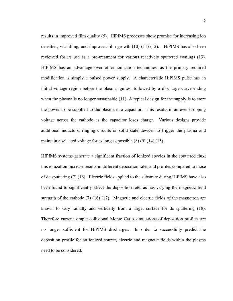
2
results in improved film quality (5). HiPIMS processes show promise for increasing ion
densities, via filling, and improved film growth (10) (11) (12). HiPIMS has also been
reviewed for its use as a pre-treatment for various reactively sputtered coatings (13).
HiPIMS has an advantage over other ionization techniques, as the primary required
modification is simply a pulsed power supply. A characteristic HiPIMS pulse has an
initial voltage region before the plasma ignites, followed by a discharge curve ending
when the plasma is no longer sustainable (11). A typical design for the supply is to store
the power to be supplied to the plasma in a capacitor. This results in an ever dropping
voltage across the cathode as the capacitor loses charge. Various designs provide
additional inductors, ringing circuits or solid state devices to trigger the plasma and
maintain a selected voltage for as long as possible (8) (9) (14) (15).
HIPIMS systems generate a significant fraction of ionized species in the sputtered flux;
this ionization increase results in different deposition rates and profiles compared to those
of dc sputtering (7) (16). Electric fields applied to the substrate during HiPIMS have also
been found to significantly affect the deposition rate, as has varying the magnetic field
strength of the cathode (7) (16) (17). Magnetic and electric fields of the magnetron are
known to vary radially and vertically from a target surface for dc sputtering (18).
Therefore current simple collisional Monte Carlo simulations of deposition profiles are
no longer sufficient for HiPIMS discharges. In order to successfully predict the
deposition profile for an ionized source, electric and magnetic fields within the plasma
need to be considered.
3
HiPIMS sources utilize several power supply designs (8) (9) (15) (19). The one clear
behavior all of these designs have in common is a high current which develops extremely
large powers for brief instances in time. A second common characteristic would be
unintentional fluctuations within the target’s current and voltage vs. time curves. Most
HiPIMS research to date has focused in the area of the improved film characteristics
provided with the increased ionized sputtered material (10), or applying the ionized flux
source in new multi-step processes (13). To date, two current/voltage fluctuations
phenomena have been explored within the HiPIMS literature, arcs (8) and a high current
phenomena induced by a preprogrammed variation in supplied power (20). The first
fluctuation to be studied in more detail was arcing. Occasionally during the pulse, the
voltage may plummet and current dramatically increase as an arc develops. In order to
prevent such behavior, arc suppression circuitry has been developed (8). The second
phenomena was initiated by a power supply design with the apparent purpose to allow
programmed high voltage waveforms of any shape with the current available for
sustained high voltage pulses (20). The inventor’s data show a marked improvement in
discharge current when the applied voltage begins to oscillate. The data would initially
seem to show that by just a small oscillation in the voltage, a dramatic increase in current
is possible. The data provided however appears to be attempting to sample an oscillation
above its Nyquist frequency, making the determination of amplitude suspect (20).
Regardless of the measurement, a basic demonstration that oscillations may drive greater
dc currents has been claimed.

4
1.2 Direct-Current Magnetron Sputtering Improvements
In order to begin to understand the HiPIMS process, it is useful to first step back and look
at what has been done with dc magnetron sputtering. In general, processing plasmas are
considered as a pair of sheaths and a uniform plasma between the sheaths (21). Direct-
current (dc) plasmas include anode and cathode sheaths, and require secondary electron
emission along with a large enough anode-cathode distance to maintain the plasma
through collisions (22). Magnetron sputtering adds a magnetic field to the dc processing
plasma allowing shorter substrate to target distances by turning the electron’s trajectory
into a helix, and thus providing the required collisions in smaller distances (23).
Unbalanced magnetron sputtering further improves the film quality through greater
plasma densities, which result from increasing the outer magnetic field strength of the
magnetron (24). Numerous types of dc magnetrons now exist, circular, rectangular,
planar, and cylindrical; some contain anodes in the center, some have floating darkspace
shields (23) (25). Each design results in different electric field patterns; the sputtered
flux in dc magnetron sputtering, however, would remain mostly unaffected. The minimal
effect on dc sputtering is related to the small percentage of ionized material, however, in
processes with highly ionized flux, such as HiPIMS the ions’ trajectory will be affected
by the electric and magnetic fields present in the magnetron plasma.
An impending process driven need to understand the role magnetic and electric fields
have within the plasma is now becoming a reality with the advent of ionized deposition
processes. In a qualitative manner the processing community can simply understand that
increased electron trapping and electron density will require increased ion trapping

5
through ambipolar diffusion and thus affect deposition profiles (16) (17). This
understanding falls clearly short of providing a predictable model applicable to various
magnetron designs or process parameter settings to generate accurate film rates and
uniformity. In order to accurately model the movement of the ions, the electric and
magnetic fields governing the ion’s path as well as collisional occurrences must be
considered. In order to predict the electric and magnetic fields the ions will encounter,
the electrical behavior of the magnetized plasma must be scrutinized.
The common thread within these HiPIMS challenges is a need for a better understanding
of the HiPIMS plasma. The focus of this dissertation is to analyze what effects and
contributions, plasma oscillations may have, in HiPIMS plasmas.
1.3 Direct-Current Magnetron Sputtering Current
Oscillations and current transport within the plasma of dc magnetrons have been a subject
of interest for many years (23) (26) (27). In 1975, Thornton theorized that diocotron type
waves and other turbulent oscillations were responsible for successful electron transport
within cylindrical magnetrons (23). Sheridan and Goree have since provided a wealth of
publications indicating the importance of collisions and ions to the magnetron behavior
(28) (29) (30) (31) (32) (33). More recently, Martines, et al. and others have renewed
some interest in reviewing the contribution of oscillations within the plasma (27) (34)
(35).
In 1989 Sheridan et al. began to investigate the concept of oscillations and how to model
the magnetron plasma (28) (31). First, Sheridan et al. performed experiments at low

6
sputtering intensities and analyzed the oscillations below 1MHz (28). Second, Sheridan
et al found that any relationship described needs to follow a dependence on the mass of
the gas (29). Third Sheridan et al. attempted to demonstrate through particle-in-cell
modeling that collisions were an important factor in electron transport, and a more likely
candidate than oscillations for the observe current flow (31).
1.3.1 Particle-in-cell (PIC) collision model
Goree and Sheridan then developed a particle-in-cell (PIC) simulation of electrons
escaping the surface of a magnetron and tracked their movements in a set of articles (31)
(32). 2-d simulations were carried out with and without collisions. However, their model
finds that significant numbers of the electrons fully use up their energy ionizing argon.
Their PIC model would result in a buildup of spent electrons within the magnetic trap.
Thus, the model does not appear to be charge/current flow balanced. Ideally each
electron would be tracked until the electron finds a wall or is otherwise neutralized.
Through more powerful computing, more self-consistent models are being developed
(36). New factor that is also missed in the PIC model is the countering magnetic field
that will develop from the electron current. As the plasma becomes denser, this may be
expected to become a significant contribution.
1.3.2 Diffusion model
Clearly there is still a need to describe the traversal and flow of electrons across magnetic
field lines beyond the expectations derived from following single electrons. Often this
gap has been filled by the semi-empirical formula of Bohm diffusion. Although Bohm

7
diffusion may approximately be derived, and describes a relationship between expected
electric fields within a plasma, the term tends to be used as a catch-all for electrons
unexpectedly penetrating magnetic barriers.
Recent experiments in analyzing plasmoid penetration of magnetic barriers have
indicated fast electron transport mechanisms exceeding Bohm diffusion (37). This
transport has been reported to be the result of oscillations in the range of the lower hybrid
frequency (38). There is therefore a need to look into the expected methods of transport
within a plasma as well as the frequencies present within magnetized plasmas.
1.4 Motivation and Objectives
Collisions and collision models fail to completely account for the behavior of magnetron
cathodes as may be seen by the lack of agreement between ionizing collisions modeled
and ionizing collisions required to maintain the plasma (30) (32) (39). These problems
are greatly magnified with the high current densities of HiPIMS.
The overall goal of this dissertation will develop a better understanding of the underlying
relationships that may result in oscillations of the power supplied during HiPIMS.
Specifically, this dissertation will:
• develop a basic model for magnetron plasmas that attempts to include
oscillations;
• explore the frequency instabilities that would be present in a magnetron;

8
• analyze the HiPIMS characteristic power curves for fluctuations and associate
these fluctuations with expected frequencies within the plasma; and
• generate a solution to the experimental solutions by applying related fields of
study.
Overall, the goal of this dissertation is to knit together the wave carrying capability of the
magnetized plasma and the observed plasma oscillations into a partial explanation for the
current carried by the plasma thus providing an improved understanding of HiPIMS and
magnetron plasmas.

9
Chapter 2 Sputtering Background
Magnetron sputtering is an important industrial process for a wide variety of products
from automobiles to semiconductors (5) (11) (24) (40). Although the basic concept of
increased current from improved path length by using magnetic trapping regions near the
cathode is well understood, the mechanisms of current flow, and the plasma behavior are
still areas of active research.
2.1 Introduction to Sputtering
Sputtering can be described as the ejection of material from a solid or molten source (or
target) by kinetic transfer from an ionized particle (41) (42). In Figure 2-1, argon atoms
are ionized and accelerated through a potential difference; the Ar+ ions then collide with
the negatively biased cathode surface, or target. Each ion collision with the cathode has
the potential to cause ejection of one or more atoms (labeled “Me” in Figure 2-1) from
the surface of the cathode. Through the process of kinetic energy transfer, the ejected
material moves away from the cathode in a linear fashion, and thus vapor atoms condense
on all surfaces in line-of-sight of the cathode. The sputtered material depositing on a
surface tends to have higher kinetic energy, imparted by the high-energy Ar+ ions, than
thermally evaporated atoms. The ejected material therefore often has higher mobility
than an evaporated material and this generally results in larger grain sizes (43), better
adhesion, and more dense film structures.

10
Figure 2-1. Sputtering of metal (Me) by ionized argon.
A wide array of materials can be sputtered regardless of their melting temperatures,
sputtering also works well with alloy sources. Although different atoms have varying
sputtering yields, a low sputtering yield material would quickly become overabundant,
and sputter at a higher rate due to an increased surface concentration. This results in film
chemistries that are quite close to those of the source material. The reader is referred to
The Materials Science of Thin Films by Ohring, (44) Thin Film Processes by Vossen and
Kern, (45) Principles of Plasma Discharges and Materials Processing by Lieberman and
Lichtenberg, (46) Handbook of Thin Film Technology by Maissel and Glang (41) and the
chapter on “Unbalanced Magnetron Sputtering” in Physics of Thin Films 18, Plasma
Source for Thin Film Deposition and Etching by S. L. Rohde, (24) for more detailed
information on sputtering and its variations.
2.2 Temperature Effects in Sputtering
Sputtering is a type of physical vapor deposition (PVD), where mostly individual atoms
collect on a substrate. Often PVD systems may also include heating, cooling and
Ar+
Me
Me

11
substrate bias capabilities in order to affect the density, uniformity, and crystallinity of
the thin film. As illustrated in Figure 2-2, heating helps nucleation of a crystalline film.
Similar to heating, the substrate bias increases the mobility of atoms on the surface of the
sample lowering the temperature at which crystalline material will be formed (47). The
substrate bias extracts positive ions out of the plasma and bombards the substrate (ion
bombardment), the voltage is slightly more negative than the potential of the plasma near
the substrate.
Figure 2-2. The effects of argon pressure and substrate temperature on film structure by Thornton
(2).
Substrate ion bombardment not only lowers the temperature at which a crystalline
material will form, but also helps to densify the material being deposited. Sputtering

12
ejects material that moves in a “line-of-sight” direction from the cathode and then
deposits on a surface. The bombarding ions act to smooth the surface by exciting the
surface atoms, thus increasing their mobility, and also by resputtering material from the
substrate. If the bombardment energy is not high enough, the film density will not
noticeably change; if the incident ion energy is too high, the film will become stressed
and may delaminate. Ion bombardment may also affect the crystallite size, and the
crystalline orientation (48) (49). Heating the substrate and ion bombardment are
important techniques, because they give the researcher more flexibility in controlling
certain film characteristics of the sputtered film.
2.3 Sputtering Techniques
There are many methods used to accomplish the sputtering of a target. Direct-current
sputtering was the original method and is named because it keeps the target at a constant
(dc) potential. Radio frequency (rf) sputtering uses a varying target potential and can be
used to sputter non-conductive materials. Reactive sputtering occurs when a gas that will
react with the target is introduced into the system and the reacted compound creates the
thin film. In general, a pulsed dc power supply is used in conjunction with reactive
sputtering. One major improvement over dc sputtering was the use of magnets behind
the target in order to increase target current and deposition rates. This is called
magnetron sputtering and can be used with either a dc or rf power supply. Each of these
methods: dc, rf, reactive, pulsed dc, and magnetron are described in more detail below.
13
2.3.1 Direct-current sputtering
The two basic requirements for dc plasma sputtering are a conductive cathode and
electron emission from the cathode. The cathode is a conductive target to which a large
negative potential voltage has been applied, while the anode is typically the metallic
chamber walls, but can also be a grounded or positively biased electrode. The processes
by which electron emission occurs and the resulting dc plasma discharge are described
below.
First, an inert gas, typically argon, is introduced into a chamber and serves as a medium
for the discharge. An ionizing event occurs similar to the ionizing event in a Geiger
counter, resulting in the formation of an Ar+ ion. If sufficiently close to the target, Ar+
ions will be accelerated towards the cathode, while the electrons near the anode are
accelerated towards the anode. The Ar+ ions colliding with the target cause ejection of
material, electrons, and x-rays, in addition to target heating. The ejected electrons are
accelerated away from the electrode through the cathode fall region (Figure 2-3), causing
more ionization, and if enough secondary electrons are produced at the target the
sputtering process becomes self-sustaining. The result is a sputtering plasma containing a
near-equilibrium number of positively ionized particles, such as ionized argon, and
negatively charged particles, such as electrons.
Figure 2-3 is a schematic sketch of a typical dc discharge. The cathode fall region is
where the largest voltage drop occurs. As the secondary electrons are accelerated away
from the cathode, the electrons will produce ionizing events as they collide with the gas
atoms in the chamber. These ionizing events will create exponentially more electrons.

14
Figure 2-3. Typical regions within a dc plasma discharge (after Lieberman and Lichtenberg) (22).
The large numbers of high-energy electrons create a region where a large number of ions
are produced (the negative glow region). Substrates are typically placed in the negative
glow region. Electrons drop most of their potential within the cathode fall, and are
slowing down as they pass through a region with more electrons than positive ions known
as the faraday dark space region, the electrons in this region collide with atoms and other
electrons slowing them down even further before entering the positive column. The
positive column is a region with a small potential gradient toward the anode, and nearly
the same number of positive and negative carriers. At the end of the positive column,
there is a region where the electron mean free path is typically larger than the distance to
the wall. In this region, all electrons are accelerated toward the wall creating a sheath
region. This region is described as the anode dark space. Thus a dc discharge will
typically have five different regions: cathode fall, negative glow, Faraday dark space,
positive column, and anode dark space. Within a magnetron sputtering cathode, most
Anode Cathode
Cathode Fall
Negative Glow
Faraday Dark Space
Positive Column
Anode dark space
Target
15
notable is the cathode fall and the dense positive column region which begins
immediately within the magnetic trap.
2.3.2 Rf Sputtering
Sputtering with rf removes the requirement that the cathode be conductive (50). In rf
sputtering, the potential applied to the target alternates from plus to minus at a high
enough frequency (>50 kHz) so that electrons can directly ionize the gas atoms, and thus
supply current to the target through capacitive coupling (51). In this case the sputtering
occurs both at the walls and at the target. The amount the walls are sputtered is
correlated with the ratio between the target and wall areas. The area that is smaller (e.g.
the target) has a higher rate of sputtering. The primary advantage of this type of
sputtering is that the target material need not be conductive, since the capacitive current
will travel through a non-conductive material.
2.3.3 Reactive sputtering
Reactive sputtering is a method to produce a compound film from a metal or metal alloy
target (52) (53) (54) (55). In reactive sputtering a reactive gas, such as oxygen or
nitrogen, is added to the inert (working) gas, typically argon. Formation of the reactive
compounds may occur in three regions, on the target, in the gas and on the surfaces.
Some of the reaction occurs at the target, a very small amount reacts in the gas, and the
remainder must react at the surfaces or be pumped away. The amount of reactive gas is
very important as an excessive amount of reactive gas reduces the sputtering rate since,
as most reactive compounds have a lower sputtering yield, and not enough gas results in

16
substoichiometric films (56). A fine balance must be made between reactive gas flow
and sputtering rate. This makes reactive sputtering an interesting challenge.
The behavior of the plasma in reactive sputtering is further complicated since different
materials emit varying amounts of electrons and have different sputtering yields; in
addition, the reactive gas will ionize along with the working gas. Reactive gases have a
number of effects on the target and the characteristics of the plasma, one of which is a
hysteresis effect (57) (58). For instance, aluminum oxide has a significantly lower
sputter yield and emits more electrons than aluminum resulting in deposition rates five
times lower than the metal deposition rate (1) (59). Different electron emissions mean
that the discharge currents may be drastically different for the same applied voltage
between the metal and the metallic compound. The changes in plasma characteristics are
thus further complicated and cannot be clearly explained for all compounds, but may help
indicate how much of the target is covered by the reactive compound. It is desirable to
sputter mostly metal in order to keep high sputtering rates, but form enough of the
metallic compound so that the film formed is stoichiometric. There are a number of
approaches detailed in the literature that try to avoid the reduction in sputtering rate for
reactive sputtering and the reader is referred to the following references for more
information (60) (61) (62) (63) (64).
2.3.4 Pulsed dc sputtering
During reactive sputtering many metals form compounds that are dielectrics. As the
dielectric forms, the target begins to build charge, and this charge reduces the potential
the plasma sees. If the dielectric layer builds up too much charge, the dielectric will

17
break down causing arcing; pulsed dc sputtering has been used in order to combat this
arcing (65). In pulsed dc sputtering the target is oscillated between an assigned negative
voltage (≅400V) and a positive voltage which is approximately 10% of the assigned
voltage at a high frequency (50-250 kHz). The positive voltage is a small percentage of
the negative set point in order to prevent sputtering of the anode. The anode may be the
walls; similar to the case with normal non-reactive sputtering, but the anode must be
protected from the sputtering target in order to act as a stable ground plane for the system
without building up a dielectric layer. One alternative method uses a second target as the
anode; in this case, the pulsing alternates which target is sputtering, and which acts as the
anode.
2.4 Magnetron Sputtering
Sputtering processes do not typically provide large discharge currents, or high deposition
rates, however the use of magnetic discharge confinement drastically changes this.
Magnets carefully arranged behind the target generate fields that trap the electrons close
to the target (66). Electrons ejected from the target are affected by an electric force due
the negative potential of the target as well as a magnetic force (“F”) due to the magnets
placed behind the target (cathode) as given by
(2-1) )( BvEF ×+= q .
18
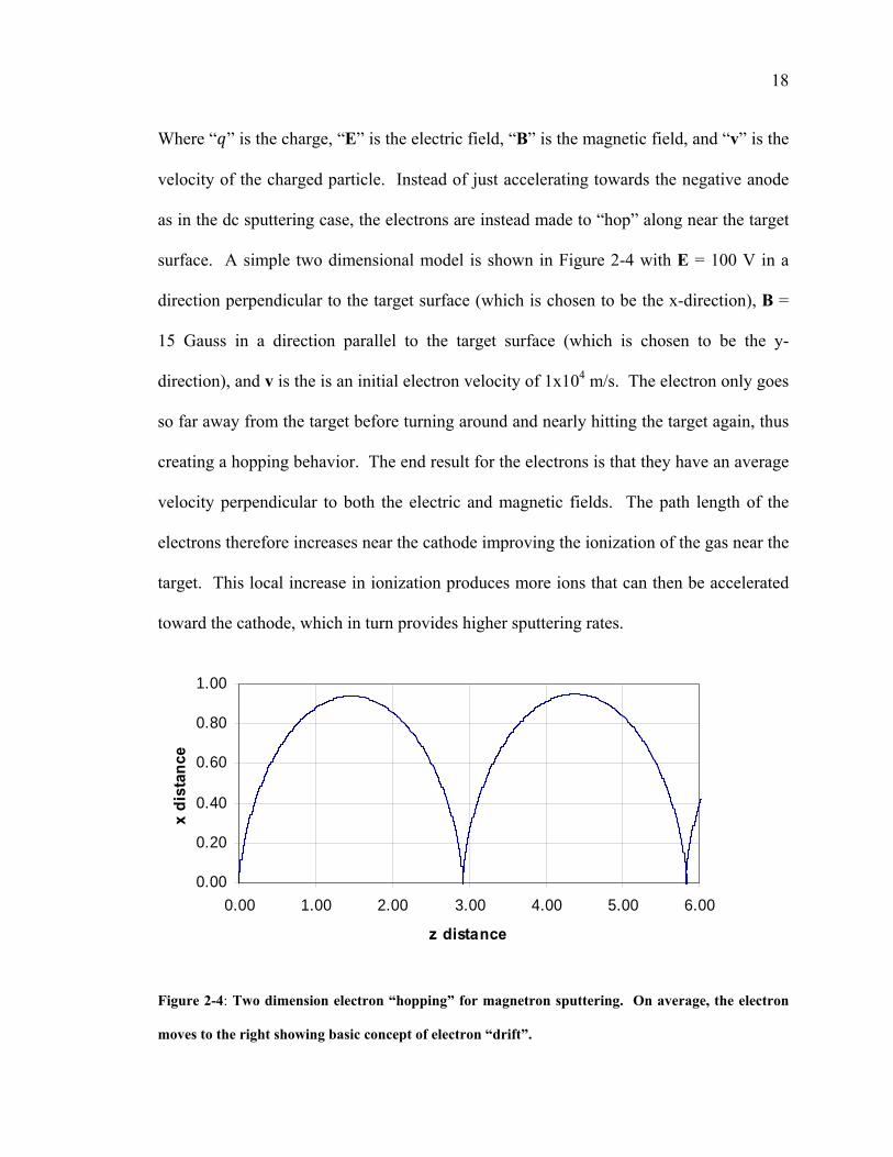
Where “ ” is the charge, “E” is the electric field, “B” is the magnetic field, and “v” is the
velocity of the charged particle. Instead of just accelerating towards the negative anode
as in the dc sputtering case, the electrons are instead made to “hop” along near the target
surface. A simple two dimensional model is shown in Figure 2-4 with E = 100 V in a
direction perpendicular to the target surface (which is chosen to be the x-direction), B =
15 Gauss in a direction parallel to the target surface (which is chosen to be the y-
direction), and v is the is an initial electron velocity of 1x10⁴ m/s. The electron only goes
so far away from the target before turning around and nearly hitting the target again, thus
creating a hopping behavior. The end result for the electrons is that they have an average
velocity perpendicular to both the electric and magnetic fields. The path length of the
electrons therefore increases near the cathode improving the ionization of the gas near the
target. This local increase in ionization produces more ions that can then be accelerated
toward the cathode, which in turn provides higher sputtering rates.
Figure 2-4: Two dimension electron “hopping” for magnetron sputtering. On average, the electron
moves to the right showing basic concept of electron “drift”.
0.00
0.20
0.40
0.60
0.80
1.00
0.00 1.00 2.00 3.00 4.00 5.00 6.00
z distance
x di
stan
ce

19
2.5 High Power Pulsed Magnetron Sputtering
The HiPIMS process is a sputtering process which results in large amounts of ionized
flux through high discharge current densities (12). The large current densities and
associated power levels are prevented from destroying the target/magnetron by applying
the power in bursts or pulses with small duty cycles thereby reducing the average power
to the cathode. The ionized flux of HiPIMS results in numerous advantages in
applications such as via or trench filling and improved film growth (10) (67). A
characteristic HiPIMS pulse (see Figure 2-5) has an initial voltage spike and a small
plateau region dependent on plasma ignition time, followed by a discharge curve ending
when the plasma is no longer sustainable (11). HiPIMS supplies store power to be
supplied to the plasma in a capacitor or bank of capacitors. This results in a dropping
voltage across the cathode as the capacitor loses charge. Various designs have been
developed to provide additional inductors, ringing circuits, arc suppression and/or solid
state devices to trigger the plasma and maintain a selected voltage for as long as possible
(8) (12) (14) (15).
HiPIMS supplies increase the significant ionized species in the sputtered flux; this
ionization shift results in different deposition rates and profiles from those of dc
sputtering (68). Statically applied magnetic and/or electric fields applied to or near the
substrate have been found to significantly affect the deposition rate for HiPIMS processes
which is not typical for DC sputtering processes (7) (16) (17). Electric fields of the
magnetron are known to vary radially and vertically from a target surface for dc

20
sputtering (18). Therefore, simple Monte Carlo simulations of deposition profiles are no
longer sufficient.
Figure 2-5. Current and Voltage vs. time for a typical HiPIMS discharge
2.6 HiPIMS and dc Magnetron Sputtering Plasmas
Studies of dc Magnetron and HiPIMS sputtering plasmas show fluctuations within the
electric field of the plasma (12) (27) (28) (35) (69) (70). These fluctuations have been
shown to have stronger occurrence at various frequencies. For example, Goree and
Sheridan have shown a strong frequency at the ion cyclotron resonance (104 Hz) (28);
and Martines et al. shows a series of frequencies in the azimuthal direction on the order
of 105 Hz (27).
0
100
200
300
400
500
600
700
800
900
0.00E+00 5.00E-05 1.00E-04 1.50E-04 2.00E-04time (s)
Volta
ge (V
)
0
20
40
60
80
100
120
140
160
180
200
Cur
rent
(A)
Cr

21
In HiPIMS numerous frequencies may be seen developing in the target voltage after the
initial ringing of the power supply has died off (71), however variation in power supply
design makes this difficult to pinpoint. HiPIMS has several intriguing plasma properties
where after an initial argon ion plasma, the plasma shifts to a metallic ion based plasma
as shown in Figure 2-6 (72) (73). This shift in ions presents interesting plasma behavior.
The films produced using this HiPIMS technique are denser than sputtered films (10)
indicating higher energy/temperature of the incoming metal flux to the substrate.
Figure 2-6. Macak et al demonstrated the shift in ions from the inert gas to metal ions (73). Optical
emmision signals for argon and titanium are overlayed with target current and voltage. The inset
shows an ion probe signal broken into argon and titanium components from the optical emission data
as deconvoluted by Macak et al (73).
Typical I-V characteristics in a dc magnetron discharge follow the formula (7) (16) (17):

22
(2-2) nkVI =
Where I is the current and V is the applied voltage and k and n are empirical constants
developed for the individual system. Typical magnetron sputtering “n” values for
effective confinement fall in the range of five to nine (17) whereas “n” values on the
order of one have been shown to indicate a lack of confinement (74). HiPIMS plasmas
have also been shown to follow the same behavior with a transition to an n=1 region at
voltages over 700 V (16) (72). In order to better understand the HiPIMS plasmas and
their parent sputtering characteristics, a careful study of the dc magnetron plasmas is
required. Studying the behavior of gasses will help develop the knowledge needed for
plasmas.

23
Chapter 3 Low Pressure Gasses
Within “Introduction to Plasma Physics” Francis Chen (75) defines a plasma as “a quasi-
neutral gas of charged and neutral particles which exhibits a collective behavior.” By
considering the “gas” a “fluid” a number of the same formulae developed for plasmas
similarly correspond to the electromagnetic behavior of free electrons in metals and other
solids. Within the present dissertation the focus is on gaseous plasmas. The basic
constituents are free electrons, at least one species of at least singly ionized ions, and
neutral gas atoms. The following chapters will develop behaviors for the above parts of
the plasma, starting with defining the behaviors of a gas, followed by basic plasma
behavior and incrementally applying previous section realizations to develop various
equations for plasmas. After which general methods for generating and maintaining
plasmas will be discussed, this will then tie in to applying plasmas to thin film deposition.
3.1 Advantages of Low Pressure
Low pressure depositions occur whenever a chamber is evacuated and includes processes
such as thermal evaporation, electron-beam evaporation, and sputtering. Vacuums have
many advantages when it comes to making thin films. These advantages stem from the
fact that pressure is inversely related to the number of molecules in a given volume as
shown by the ideal gas law:
(3-1) NKTPV =
24
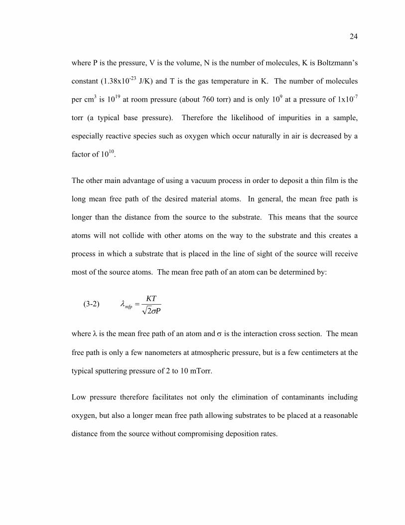
where P is the pressure, V is the volume, N is the number of molecules, K is Boltzmann’s
constant (1.38x10⁻²³ J/K) and T is the gas temperature in K. The number of molecules
per cm3 is 1019 at room pressure (about 760 torr) and is only 109 at a pressure of 1x10⁻⁷
torr (a typical base pressure). Therefore the likelihood of impurities in a sample,
especially reactive species such as oxygen which occur naturally in air is decreased by a
factor of 1010.
The other main advantage of using a vacuum process in order to deposit a thin film is the
long mean free path of the desired material atoms. In general, the mean free path is
longer than the distance from the source to the substrate. This means that the source
atoms will not collide with other atoms on the way to the substrate and this creates a
process in which a substrate that is placed in the line of sight of the source will receive
most of the source atoms. The mean free path of an atom can be determined by:
(3-2) P
KTmfp
σλ
2=
where λ is the mean free path of an atom and σ is the interaction cross section. The mean
free path is only a few nanometers at atmospheric pressure, but is a few centimeters at the
typical sputtering pressure of 2 to 10 mTorr.
Low pressure therefore facilitates not only the elimination of contaminants including
oxygen, but also a longer mean free path allowing substrates to be placed at a reasonable
distance from the source without compromising deposition rates.

25
3.2 Gases at Low pressures, Collision Frequency and Mean Free Path
Derived
In order to understand plasmas the concept of a gas and fluid must first be described. A
gas may be considered a fluid with no local ordering of the atoms/molecules, where the
atoms/molecules may be considered individual particles. These particles move about
with a distribution of velocities colliding with each other and the chamber walls. The
momentum delivered to the walls from the atom’s velocity is generally described as a
pressure. The velocity distribution is associated with the atom’s temperature through a
Maxwell Boltzmann relationship:
(3-3)
where “ ” is the number of molecules as a function of velocity, “ ” is the molecules per
volume, “ ” is the mass, “ ” is boltzmann’s constant, and “ ” is the temperature in
Kelvin.
3.2.1 Gas pressure, temperature and atom density relationship
Atoms/molecules in a gas have energy associated with their velocity. Each atom’s
velocity is not necessarily exactly the same; rather the atoms produce a distribution of
velocities. This distribution will change with temperature, and there are a number of
ways to describe such a distribution. The pressure may be related to the distribution of
the gas atoms at a given isothermal temperature by the formula:
(3-4) or also
26
Where is pressure, is number of atoms, is Boltzmann’s constant and is
temperature in Kelvin. The above formula may be rewritten as the relationship:
(3-5) 3.25 10
with in atoms per cubic centimeter and p in Torr at standard temperature.
3.2.2 Collision frequency and mean free path
Atoms within a gas are typically traveling with high velocity. The velocities of the atoms
vary and may be predicted to approximate a Maxwell Boltzmann distribution described
previously. The distribution can be described using the terms of the most probable
velocity (u ), the average velocity (u), and the root mean square velocity u . The
values for each are different due to the large tail at higher velocities in the distribution
and given by the formulae (22):
(3-6) u
(3-7) u
(3-8) u
where, “ ” is the temperature and “ ” is the mass of the gas atoms. At room
temperature for argon this results in average velocities on the order of hundreds of meters
per second. It is highly unlikely however, for an atom to travel a distance of hundreds of
meters in a single direction in a second due to the presence of other atoms for collision.
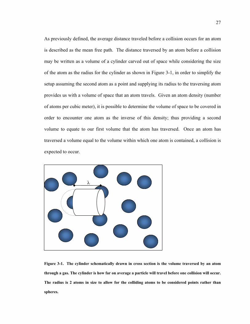
27
As previously defined, the average distance traveled before a collision occurs for an atom
is described as the mean free path. The distance traversed by an atom before a collision
may be written as a volume of a cylinder carved out of space while considering the size
of the atom as the radius for the cylinder as shown in Figure 3-1, in order to simplify the
setup assuming the second atom as a point and supplying its radius to the traversing atom
provides us with a volume of space that an atom travels. Given an atom density (number
of atoms per cubic meter), it is possible to determine the volume of space to be covered in
order to encounter one atom as the inverse of this density; thus providing a second
volume to equate to our first volume that the atom has traversed. Once an atom has
traversed a volume equal to the volume within which one atom is contained, a collision is
expected to occur.
Figure 3-1. The cylinder schematically drawn in cross section is the volume traversed by an atom
through a gas. The cylinder is how far on average a particle will travel before one collision will occur.
The radius is 2 atoms in size to allow for the colliding atoms to be considered points rather than
spheres.
λ

28
Thus yielding the equation:
(3-9) or 1
where is the collision cross-section defined in this case, by , is the length of
the mean free path and is the density. (Note: This equation is another form of equation
(3-2) where ng has been substituted in for p/KT). By applying the average velocity “u” of
the atoms in the gas we can develop an expression for how long before a collision occurs
“ ” and how frequently collisions occur “ ” with the equations (22):
(3-10) and u
Free electrons and ions within a plasma have the same behaviors as the gases, but with
the additional twist of interactions that result from their charge. This produces new types
of collisions such as electron-neutral, ion-electron and ion-neutral, as well as cumulative
behaviors from the electric and magnetic interactions of charged particles.
Collisions are key to understanding of dc sputtering and HiPIMS plasmas. Energetic
electrons collide with argon atoms generating argon ions. These ions are accelerated
toward the cathode with enough velocity to collide with and eject material for deposition
as well as more electrons for ionization. The collision frequency also plays an important
role in the behavior of waves and diffusion. Now that low pressure gases have been
developed, the physical description of a plasma may be described.

29
Chapter 4 Plasma Definitions
A gas behaves as a plasma whenever there are enough ions to screen out an electric field.
For example, if a positively charged plate is placed within a plasma, positively charged
ions will be repelled, and negative charged ions and electrons will be attracted. This
movement of charge will occur until the charged plate has enough surrounding charges
within the plasma to negate the plate’s effect on the electric field within the plasma. The
movements of these charges all depend on forces. The equation governing most of these
behaviors is the force equation which in general terms may be written as (22):
(4-1) mn ·
where, m is the mass, n is the density and is the velocity vector. The force equation
above relates the acceleration of the particles within the fluid to the forces from electric
and magnetic fields; pressure gradients; and collisions.
In addition to Equation (4-1), the continuity equation also plays a role in governing
charge motion and it states that the number of particles in a volume can change only
when a flux of particles crosses its enclosed surface, described mathematically by the
equation:
(4-2) · 0.

30
4.1.1 The Debye length
The distance an electric field penetrates into a plasma is related to the Debye length.
Using the plate example from the previous section, the distance of the plate’s influence
on the electric field within the plasma is defined as the Debye length (see Figure 4-1).
Figure 4-1. Negative charges are schematically drawn depicting a plasma attracted to and effectively
shielding a positively charged plate. Dotted line indicates approximate Debye length.
The freely moving ionized particles within the plasma will develop an oppositely charged
region next to a charged plate. The particles providing the charge however, still have
their thermal energy and therefore velocity. This prevents the charged region from
becoming infinitesimally small as the free electrons move about due to their thermal
energy. The equation describing the Debye length is:
(4-3)
V + -
++++++++++
-
-
-
-
-
-
-
-
-
-

31
4.1.2 The Boltzmann relation
The Debye length equation relates the energy of the electrons ( ) to the electric
potential ( ) within the plasma from Poisson’s equation
(4-4) 4 ,
through the Boltzmann relation
(4-5)
where is the electron density, and is the ion density. The Boltzmann relation is
generated by looking at the behavior of the electrons within the plasma in equilibrium
due to the interactions between electric field forces and pressure gradients applied to the
electron fluid.
4.1.3 Boltzmann relation derivation
The attraction and expected movement of the charged particles to the plate of Figure 4-1
generates a pressure (change in density) imbalance on the electrons within the plasma
generating a force density ( ) on the charged particles which is counter balanced by
the force applied by the electric field ( ) created by the charged plate resulting in the
sum of force densities of (22):
(4-6) 0,
assuming an isothermal state and using equation (3-4) which applies when changes in
pressure are on a slow time scale, and equation (4-6) changes to:

32
(4-7) 0
Recognizing that ln , and by removing a factor of equation (4-7) may be
rewritten as:
(4-8) ln 0
then integrating provides the result:
(4-9) ln
where “ ” is a constant, rearranging terms, solving for , and recognizing the initial
condition of no electric field should result in a density of the plasma ( ) generates
the previously discussed Boltzmann relation:
(4-10)
As shown, the Boltzmann relation assumes that the electrons are isothermal within the
plasma, this assumption means that the electron temperature throughout the plasma is
expected to be the same temperature; and that any waves that are to be considered, are
slow enough to allow the electrons to distribute the energy, maintaining the constant
temperature assumption.
4.1.4 Debye length derivation
By substituting the Boltzmann relation into Poisson’s equation (4-4), and assuming the
ions are stationary such that the result is (22):

33
(4-11) 4
then, by expanding the exponential through a Taylor series ( ∑! ) we get:
(4-12) 4 1 1
Assuming that is much less than one, the system may be linearized by dropping the
terms after “n=1” as insignificant (for 0.1 the “n=2” term is only a 5% change and
at 0.01 the change is half a percent) equation (4-12) becomes:
(4-13)
By recognizing the form of the double derivative depending on itself, a function of
potential fitting this description would be of the form the double derivative
of which is:
(4-14)
replacing the generic term “c” and defining this term as the Debye length , and placing
equation (4-13) into the form of equation (4-14) using the equation (previously given
in equation (4-3) ) for becomes:
(4-15)

34
4.1.5 Boltzmann and Debye length assumptions and limitations
This characteristic length for an electric charge’s influence on a plasma has been
determined using several assumptions. The first assumption is the linearization of the
exponential within Boltzmann’s relation which assumes 1. Second, the Boltzmann
relation itself assumes isothermal electrons with no drift velocity. Finally the assumption
is made that the ions are stationary due to having a mass three to four orders of
magnitude greater than the electrons. Nevertheless, the Boltzmann relation and the
Debye length provide two quick and simple methods for comprehending the behavior of
the plasma, and its interaction with electric fields. The plasma is quasi-neutral allowing
small electric fields to propagate. Fields applied to a plasma will reduce by about two
thirds (1-e-1) every Debye length, and this is achieved by relatively small differences in
the density of electrons to ions that counteract the applied field according to the
Boltzmann relation.

35
Chapter 5 Plasma Sheath
As previously discussed, a set of ions, electrons or neutral gas atoms can be expected to
follow a Boltzmann distribution for their individual velocities. As shown in equation (3-
7), the average velocity of the particles is inversely proportional to their mass. The net
result of this mass dependence is the treating of the ions as “stationary” and considering
only the electrons as having a thermal velocity. Since the electrons are moving faster
than the ions it can be expected more electrons hit the walls or other objects within the
system more often than the ions. As electrons are lost, however, the potential of the
system will shift positive as there are now more ions than electrons within the plasma.
Eventually the system reaches an equilibrium state where the electrons bombarding an
object where the flux Γ is equal to the ions bombarding an object Γ such that Γ Γ ,
due to the net positive charge of the plasma attempting to hold in the electrons from
walls. A plasma as shown earlier with the Debye length as in equations (4-14) and (4-
15), attempts to shield out electric fields from the plasma, thus pushing the potential drop
and loss of electrons close to the walls (within a few Debye lengths of the wall). The net
results are 1) a small region where the electron density is less than the ion density and 2)
for a wall with zero net current, the number of electrons hitting the wall is equal to the
number of ions hitting the wall.
5.1.1 Plasma Sheath as a dielectric
The plasma sheath, the region where most of the potential is dropped, contains fewer
electrons and ions than the bulk plasma; and this region may be described by a number of

36
approximations. The first simple approximation for the sheath is assuming a thin layer of
a vacuum absent of any ions or electrons. The approximation assumes the number of
electrons and ions within the sheath are so small, that their contribution is negligible as
shown in Figure 5-1 (22) (76).
Figure 5-1. A schematic representation of a plasma sheath between a wall and a plasma; and the
plasma density profile is shown as a cutoff with the ions and electrons dropping to zero at the sheath
edge. The sheath thickness is “s”.
n0
x
n
wall sheath plasma
s
n = ne = ni

37
This approximation results in an air dielectric between two conducting surfaces, the wall
and the plasma. The capacitance ( of the sheath may then be written as:
(5-1)
Where s is the sheath thickness is the dielectric constant of a vacuum; is the area of
the sheath and is the thickness of the sheath.
5.1.2 Plasma pre-sheath and floating wall potential
A second approximation describing the sheath would be to reduce the electrons faster
than the ions as shown in Figure 5-2, and to gradually reduce the plasma density within
the sheath rather than abruptly cutting off the plasma. A floating wall would then have a
potential ( ) according to the following equation:
(5-2) ,
where is the electron temperature, and are the ion and electron masses
respectively. This shows that a floating wall would be expected to have a linear behavior
with respect to the electron temperature of the system.

38
Figure 5-2. A description of the plasma sheath using a pre-sheath region of reducing plasma density
followed by a sheath containing more ions than electrons due to the difference in the thermal velocity
of ions and electrons is schematically depicted. The electron (dotted line) and ion density (solid line)
are equal within the pre-sheath and bulk plasma.
The floating potential is derived by setting the electron flux to the wall equal to the ion
flux at the wall where (22):
(5-3)
is the ion flux where it is assumed the ions have the uniform Bohm velocity , and the
electron density may be described by (22):
(5-4)
n0
x
n
wall sheath plasma
s
pre-sheath
ne ni

39
that is assumed to be a Maxwellian distribution of electron velocities due to their thermal
energy. At the sheath-presheath edge the plasma density is expected to have become
reduced to a value from the bulk plasma density through the presheath due to a small
potential where the approximation of ne=ni still holds. The Bohm velocity may be
written as (22):
(5-5)
The Bohm velocity is the speed that the ions have been accelerated to during the pre-
sheath region, where the assumption of the ions and electrons quasineutrality may still be
assumed to hold, but that a small electric field is still present causing the ions to be
accelerated, and the electrons to follow the Boltzmann relation. The Bohm velocity is a
minimum velocity that the ions need entering the sheath in order for the ion density not to
decrease too dramatically. This is caused by applying the conservation of energy to the
assumption of constant flux within the sheath. Given that electrons initially escape more
readily from the plasma, the plasma is slightly positive and therefore the potential is
negative as the ions approach the wall within system setting up the energy conservation
equation (22):
(5-6) Φ x ,
where is the ion velocity at the edge of the sheath, and since the electric field is
negative, the velocity at any point is increasing as the ions approach the wall.
Unless ions are being created and destroyed, the flux may be assumed to be constant. A
constant flux means if there is an increase in velocity; the density must decrease to

40
maintain a constant flux. The equation describing this assumption is a form of the
continuity equation (4-2) (22):
(5-7)
where the flux at the sheath edge “ ” is equal to the density at any given
position times the velocity at that same position. Solving equation (5-6) for
velocity at any point in the sheath “ ” becomes (22):
(5-8)
Figure 5-3 shows the ion velocity curves with various initial sheath ion velocities as the
ions are accelerated across the sheath by the sheath potential. As the initial ion velocities
increase, the contribution that the sheath potential acceleration provides to the ions’ final
velocity is reduced.

41
Figure 5-3. The theoretical ion velocity dependence on initial ion velocity. Initial ion velocities of:
zero, half the bohm velocity (KT/M), the Bohm velocity, and twice the Bohm velocity, are shown. As
the ion velocity reaches the Bohm velocity, the sheath has a smaller relative influence.
If the ions had no or a very small initial velocity the flux caused by the ions would also
be very small. The less effect the sheath potential has on the ions, the smaller the change
in ion density that is required to maintain the assumption of a constant flux across the
sheath. The effect the assumption of constant flux and the accelerating ions may be seen
by applying the ion velocity from equation (5-8) into equation (5-7) the ion density
behavior within the sheath will follow:
(5-9) 1
Ion
velo
city
with
in sh
eath
Arb
itray
Uni
ts
Sheath Potential----> Towards wall
no initial
half
kt/m
2kt/m
kt/2m

42
Figure 5-4 shows the ion density through the sheath, using the assumption of constant
flux. The effect of initial velocity may be clearly seen in the plasma density. The
electron density has been assumed to follow the Boltzmann relation from equation (4-10),
and is also plotted as a reference point. Only solutions that have more ions than electrons
meet the criteria of the assumptions for the negative electric field.
Figure 5-4. Ion density for various initial velocities with respect to the Bohm velocity (kT/M)
compared to the electron density (Ne). Velocities graphed are zero initial velocity, half the bohm
velocity, the Bohm velocity, and twice the Bohm velocity. Only the Bohm velocity meets the initial
assumption that the number of ions is equal to the number of electrons and also maintains the
assumption of more ions than electrons (Ne) within the sheath.
ion
dens
ity w
ithin
shea
thA
rbitr
ay U
nits
Sheath Potential----> Towards wall
no initial
half
kt/m
2kt/m
Ne
kt/2m

43
A minimum velocity is required in order to maintain the constant flux assumption while
also maintaining the assumption of more ions than electrons within the sheath. This
minimum ion velocity assumes the Boltzmann relation is accurate for the presheath
electrons, which assumes isothermal and uniform electron densities.
The electron flux is developed from the assumption that the electrons have a distribution
of velocities and directions from their temperature which outweighs any drift velocity.
The average speed of the distribution is given by equation (3-7), ; and the
number of electrons flowing out in one direction is given by (22) (75):
(5-10)
So, by setting Γ Γ and substituting in for the Bohm velocity the relationship becomes
(22):
(5-11)
then by applying Boltzmann’s relation for the number of electrons, and setting the
potential to the potential of the wall with respect to the sheath-presheath edge, the result
is (22):
(5-12)
then taking the natural log and solving for the wall potential results in previously given
equation (5-2) (22):
44
(5-13)
This potential therefore assumes: the drift velocity of the electrons is small with respect
to the electron temperature; the electron temperature is uniform; the electrons are
isothermal; and that there is no ionization within the sheath. The potential at the wall
5.1.3 Child-Langmuir law sheath
The Child-Langmuir law sheath assumption allows the derivation of the Child-Langmuir
law of “space charge limited” current in a planar diode. The assumptions are: ignore the
contribution of electrons to the sheath current; equate the current to the flux of ions
across the sheath; and assume the energy developed by the ions in the presheath is
insignificant in comparison to the energy developed within the sheath. The resulting
Child-Langmuir law formula for current in a “space charge limited” diode is (22):
(5-14)
Where J is the ion current, is the permittivity of free space, is the potential applied
to the electrode, and is the sheath thickness. This defines the expected non-linear
relationship for plasma diodes. The ion current is simply the flux of ions as in equation
(5-3), multiplied by the charge of the ions, which assuming singly ionized species and
constant flux results in (22):
(5-15)
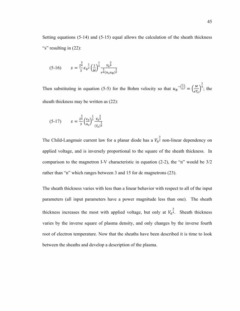
45
Setting equations (5-14) and (5-15) equal allows the calculation of the sheath thickness
“s” resulting in (22):
(5-16)
Then substituting in equation (5-5) for the Bohm velocity so that ; the
sheath thickness may be written as (22):
(5-17)
The Child-Langmuir current law for a planar diode has a non-linear dependency on
applied voltage, and is inversely proportional to the square of the sheath thickness. In
comparison to the magnetron I-V characteristic in equation (2-2), the “n” would be 3/2
rather than “n” which ranges between 3 and 15 for dc magnetrons (23).
The sheath thickness varies with less than a linear behavior with respect to all of the input
parameters (all input parameters have a power magnitude less than one). The sheath
thickness increases the most with applied voltage, but only at . Sheath thickness
varies by the inverse square of plasma density, and only changes by the inverse fourth
root of electron temperature. Now that the sheaths have been described it is time to look
between the sheaths and develop a description of the plasma.

46
Chapter 6 The Plasma as a Fluid
The basic diffusion and fluid equations allow the development of equations to describe
the diffusion behavior of the plasma which is a critical step in understanding the HiPIMS
and sputtering behavior.
6.1 Diffusion in a plasma
The application of the diffusion coefficient is one method used to develop an expression
for the plasma as fluid motion. As the plasma is a fluid, Fick’s first and second laws of
diffusion can apply. Fick’s first law suggests that flux will flow away from a high
concentration to a low concentration. Fick’s first law may be written as:
(6-1)
Where Γ is the flux, D is the diffusion coefficient, and n is the density.
Fick’s second law describes the change in density over time due to a concentration
gradient as:
(6-2) ,
where is the change in density with respect to time. In effect, a plasma will have a
driving force which will be attempting to make the plasma uniform over the region within
which it is contained. A second driving force within plasmas is the electric field. This
leads to the particle flux equation (22):
47
(6-3) ,
where is the mobility constant for that species. “ ” may be found by taking the charge
of the species and dividing by the mass “ ” and the collision frequency ” ”:
(6-4)
And the diffusion constant may be found by:
(6-5) and for hard sphere scattering
with being the Boltzmann constant and temperature respectively. The components of
the electric field force are seen in the first term of equation (6-3). The second term is the
pressure from a concentration gradient.
These basic plasma behaviors include the decay of variations in plasma densities.
Variations in plasma density should be expected to disperse over time, and more complex
and/ higher order functions may be expected to die out first very similar to the way higher
overtones are the first to die out when a piano key is struck.
6.2 Charge Balance and Ambipolar Diffusion
There are a large number of charged particles within the sputtering plasma, and even
more within a HiPIMS plasma. The plasma contains nearly an equal number of electrons
and ions. This behavior leads to the assumption of “quasi-neutrality”. It is assumed that
the number of electrons is nearly equal to the number of ions.

48
The expectation of quasi-neutrality also leads to the expectation that motion of either
electrons or ions will carry the other along through ambipolar diffusion.
By application of equation (6-3) for diffusion of electrons and ions, and assuming nearly
equal number of electrons and ions, and no external electric fields; the following
ambipolar diffusion equations may be developed (75):
(6-6)
and,
(6-7) 0
Where is the ambipolar diffusion constant; which consists of (75):
(6-8)
Where is the ion mobility, is the electron mobility, and and are the electron
and ion diffusion constants of equations (6-4) and (6-5).
6.3 Magnetic Effects in a Plasma
6.3.1 Magnetic effects on a particle
Magnetic fields have a direct effect on the capability of electrons and ions to move within
a plasma through the basic force equation:
(6-9)

49
The basics of which may be seen in equation (4-1). The magnetic field applies a force
perpendicular to both the velocity and the magnetic field. The net result is the magnetic
field creates a circular motion on top of whatever trajectory the system had initially.
Since the magnetic field is always applying a force to the perpendicular component of
velocity, this becomes basic circular motion with the magnetic field providing the inward
force that maintains an object in circular motion. The end result being:
(6-10) | |,
which develops the Larmor radius for a charged particle as:
(6-11) .
is the angular cyclotron frequency which is:
(6-12)
Key facts to note are that frequency is not velocity dependent, larger masses increase the
Larmor radius and that the Larmor radius decreases with increasing magnetic field.
6.3.2 Magnetization of a plasma
Magnetization of a plasma occurs when the geometry of the system allows the charged
particles within the plasma to successfully complete a Larmor radius. Electrons being
relatively light may be considered “magnetized” within as little as a 100 gauss field.
The Larmor radius for an electron is approximately:

50
(6-13) . √ ,
with in gauss and in electron volts. The magnetization of electrons freezes the
electrons in place within the magnetron helping to generate the higher density plasma
glow close to the cathode surface.
6.3.3 Magnetic field effects on diffusion
The magnetic torus that keeps a dense plasma close to the sputtering cathode’s surface is
a large gradient in plasma density, and therefore may also be expected to be affected by
diffusion. By applying the diffusion coefficients definitions to equation (4-1) while
including a magnetic field, the resulting flux equation is (75):
(6-14) Γ
Where and are the perpendicular mobility and diffusion coefficients, and are
defined by (75):
(6-15)
and (75),
(6-16) 2
2 2 2

51
where is the cyclotron frequency from equation (6-12), and is the time for one
collision to occur. The velocities and are the drift and diamagnetic drift
velocities where (75):
(6-17)
is the drift and (75),
(6-18) B
is the diamagnetic drift.
The end result being that the flux of the charged species perpendicular to the magnetic
field lines have the drift velocities’ contribution reduced by collisions, and mobility and
diffusion constants are increased with collisions; the exact opposite is true for flux in
nonmagnetic fluxes. The mobility and diffusion terms in the perpendicular flux equation
are also inversely proportional to the magnetic field squared.
6.3.4 Bohm diffusion
Experimental data on magnetic plasmas has developed a formula for the perpendicular
diffusion rate that is different from above equation (6-16). Bohm diffusion depends
inversely upon magnetic field only as B rather than B squared as shown (75) (22):
(6-19)
This diffusion constant does not appear to depend upon density, or collisions, and the
time constant for Bohm diffusion is approximately (22):

52
(6-20)
Where N is the total number of charge carriers in the plasma. Bohm diffusion has been
attributed to turbulent disturbances within plasma generated by instabilities within the
plasma. The instabilities occur from waves within the plasma absorbing free energy
within the system. These instabilities may be fueled by streaming ions or electrons, and
variations in temperature etc.
6.3.5 Drift velocities in a fluid
In the theory for polarization drift for a magnetized plasma with perpendicular magnetic
and changing electric fields E(t), the center of motion of an electron has a polarization
drift velocity in the same direction as the electric field due to the changing drift velocity
perpendicular to the electric and magnetic fields. The polarization current would follow
the equation (22):
(6-21) dtdE
BnmM
J p 20
0)( +=
A number of papers have been published recently discussing self polarization and other
methods for electron transport for plasmoids as they approach a magnetic barrier (37)
(38). The mechanisms are self polarization and magnetic expulsion. An oversimplified
way to define “self polarization” is to consider the ions continuing past a barrier
unattainable for the electrons. The plasmoid then develops a change in electric field as
the ions get exposed. The changing electric field now develops a polarization drift in the

53
electrons which then drives a set of electrons past the previously unattainable magnetic
barrier.
A second possibility in order to overcome the barrier is for the plasma to develop a
magnetic field counter to the field the plasma sees being applied by external forces. This
would occur through the diamagnetic current of the plasma. This current attempts to
expel lines of flux from the plasma similar to superconducting fluids.
The drifts and characteristic frequencies of a magnetized plasma can develop into
oscillations within the plasma. In order to describe these oscillations, the equations of
magnetized particles and their effects on ionized fluids will now be applied assuming a
small sinusoidal variation.

54
Chapter 7 Waves and Plasma Oscillations
7.1.1 Sinusoidal equations of particle motion
In order to look at the frequencies that occur within the plasma, it would be helpful for
the notation for the description of the plasma as a fluid to be in terms of sinusoidal
behavior. The sinusoidal behaviors are expected to be small, with an angular frequency
of oscillation “ ” and a wavenumber “ .” This results in replacing: time derivatives
with the term “ ”; and the gradients by the term “ ” for a given direction of
oscillation in the x direction. For example the oscillations of the velocity, electric field
or density may be described as sinusoidal. The result is that the force equation (4-1)
neglecting collisions and magnetic fields for the moment may be written as (75):
(7-1)
And the equation (4-2) for continuity becomes (75):
(7-2)
And for an electric field that may be described by the gradient of the electric potential
(75):
(7-3)
7.1.2 Development of the plasma frequencies
Within plasmas, especially magnetized plasmas, a whole host of various frequencies are
possible to develop. A first step in understanding that waves and oscillations will occur

55
within a plasma is to first consider a hypothetical situation of a slab of initially neutral
plasma with a plasma density of . Now imagine applying a force that pulls all the
electrons to the left just a small bit “ ,” and that “ ” is a function of time as shown in
Figure 7-1.
The jostling of the electrons uncovers the slower ions on the right hand side, and
generates a set of uncovered electrons on the left hand side. After this initial shove, the
plasma is let go and observed.
Figure 7-1. A displaced electron cloud (downward cross-hatching) is schematically drawn over a set
of stationary ions (upward cross-hatching). An enclosed surface for finding the electric field over a
region using Gauss's law is also drawn.
-
-
-
-
-
+
+
+
+
+
Q enclosed electrons
ions
both

56
The plasma now has a charge on one side, developing a field. Assuming a semi-infinite
slab of plasma, there is only an electric field inside the plasma, and apply gauss’s law to
find that electric field resulting in (22):
(7-4) ,
is the dielectric constant permittivity of free space. The electric field applies an
electric force to the electrons, and an acceleration (22):
(7-5) .
By applying these two equations, one gets (22):
(7-6) ,
which has the form of a double derivative equal to itself times a constant (indicating
simple harmonic motion), thus recognizing simple harmonic motion and the angular
frequency for the electrons as (22):
(7-7) ,
where is the mass of an electron. Similarly there is an angular frequency for the ions
(22):
(7-8) .
The base frequencies of the plasma are the plasma electron frequency and the plasma ion
frequency: ωp =2πfp, and follows the relationships described above in (7-7) and (7-8).

57
Previously, equation (6-12) (the cyclotron frequency) demonstrated an angular frequency
for charged particles in a magnetic field. There will be at a minimum two cyclotron
frequencies within a plasma as well. One for the electrons (22):
(7-9)
And one for the ions (22):
(7-10)
where q is the charge of the particle, B is the field, and M is the mass of the ion or the
electron for ωci and ωce respectively. A magnetized plasma therefore has four basic
frequencies, the electron and ion plasma frequencies (equations (7-7) and (7-8)) and the
electron and ion cyclotron frequencies (equations (7-9) and (7-10)).
There are a number of other frequencies and waves that may propagate from a
magnetized plasma. These include ion acoustic waves, lower hybrid waves, electrostatic
ion cyclotron waves, Alfvén waves, and Magnetosonic waves. To further complicate the
issue, the magnetic fields vary in strength and direction within the area of interest from
400 to 50 gauss and therefore each “base” frequency becomes a range of frequencies.
7.1.3 Electrostatic wave propagation
Initially the condition of electrostatic wave propagation may sound like a misnomer;
however this behavior is based on the behavior of a sound wave. Electrostatic waves
propagate a pressure wave that is exchanging heat energy and electric energy. The
electric fields are in the same direction as the propagation direction, which is the clue to

58
how this wave does not necessarily have a magnetic component. Imagine an electron
reacting to the changing electric field, this electron alone would clearly be generating a
magnetic field as a charged particle that is accelerating. This motion’s magnetic field
however, would be counter balanced by electrons moving toward the same position as the
first electron, but from the opposite side, thus generating pressure without a net magnetic
field that will adiabatically compress and exchange energy with the electric field setup by
the ion’s lack of mobility in comparison to the electrons.
Another way to look at the concept is that the electric field of this wave is parallel to the
propagation direction. The magnetic field is the cross product of the propagation
direction and the electric field. This results in no net magnetic field since the cross
product is zero.
The classic way to observe electrostatic behavior is through the ion acoustic wave. By
starting with the fluid equation (4-1) for ions, and assuming: sinusoidal oscillations, the
electric field is the gradient of the potential, and compressions of the ion wave are planar,
resulting in the following sinusoidal equation result (75):
(7-11)
(7-12)
Solving for in equation (7-12) and replacing in equation (7-11)
(7-13)
A linearized expansion of the Boltzmann relation is:

59
(7-14) or
and the continuity equation for from equation (7-2):
(7-15)
Using equations (7-14) and (7-15), equation (7-13) then results in: (75)
1
(7-16)
Equation (7-16) is the electrostatic wave behavior for ions in a magnetized plasma with
collisions for the ions. Ignoring collisions, the resulting equation is (75):
(7-17)
The non magnetized ion acoustic wave propagation results in the equation (75):
(7-18)
Equations (7-16), (7-17) and (7-18) therefore summarize the electrostatic wave behavior
for ions under various assumptions.

60
7.2 The plasma as a Dielectric
There are many methods to electrically describe various portions of a plasma within the
confines of the lab. A laboratory plasma without a magnetic field will be contained by a
sheath at its boundaries, which we will consider the boundaries as two plates, and
therefore two sheath regions. To a first approximation, an electrical analogy to this
system would be a capacitor for each of the two sheaths, and an inductor or a capacitor
for the plasma dependent on the waves’ frequency (77). The dielectric constant of the
plasma (εp) is described by the equation (22):
(7-19) 1
where ε0 is the permittivity of free space, ωpe is the electron frequency, ω is the
frequency of the incoming wave. This plasma dielectric equation is valid for (1) non-
magnetized plasmas and (2) electric fields parallel to magnetic field lines. Below the
plasma frequency the plasma acts as an inductor (negative dielectric constant), while
above the plasma frequency, the plasma acts as a capacitor.
7.2.1 Electromagnetic wave propagation
Generally, this shows that for frequencies less than the plasma frequency, waves should
be stopped at the plasma surface and prevented from entering. By applying the plasma
dielectric constant to the following equation (22):

61
(7-20)
it can be found that waves stop propagating when the electric field becomes zero. This
may be seen through the dispersion relation for the electromagnetic waves of the above
dielectric constant (22):
(7-21)
which will become zero at frequencies below the plasma frequency ( ).
7.2.2 Dielectric tensor
The above description works for dielectric constants that do not vary with respect to
angle or polarization within the material. The magnetized plasma however, has an
anisotropic behavior that also has off-axis dependencies due to the cross product effect
the magnetic field has on the velocity of ions and electrons. The solution is to represent
the plasma medium using a dielectric tensor where (22):
(7-22) ⎟⎟⎟
⎠
⎞
⎜⎜⎜
⎝
⎛ −= ⊥
⊥
||
0
0000
κκκκκ
εε x
x
p jj
Where κ is the dielectric constant for perpendicular to field lines, κx is the effect
perpendicular electric field in one direction has on the remaining perpendicular direction
and κ is the dielectric constant parallel to field lines, which are described in detail
elsewhere. (22) When including ions, and ignoring collisions the dielectric constants
become (22):

62
(7-23) 22
2
22
2
1ci
pi
ce
pe
ωωω
ωωω
κ−
−−
−=⊥
(7-24) 22
2
22
2
ci
pici
ce
pecex ωω
ωωω
ωωω
ωω
κ−
−−
=
(7-25) 2
2
|| 1ωω
κ p−=
and by letting (22):
(7-26) xl
xr
k κκκκκ
+=−=
⊥
⊥
one can apply this complex dielectric constant to an electromagnetic wave propagating
within the medium. Using N= k/k0 one can develop an equation describing the dispersion
of the waves within the plasma using (22):
(7-27) ( )( )
( )( )lr
lr
NNNN
κκκκκκκ
θ−−−−
−=⊥
2//
2
22//2tan
where θ is the angle of propagation with respect to the magnetic field lines. This
representation assumes no collisions. From equation (7-27), it is evident that there are
various frequency solutions depending on the angle of propagation.
7.2.3 Geometric oscillations
The frequencies developed in prior sections deal with resonances for an unbounded
generic plasma. This would be the equivalent of developing the propagation expectations
of a sound wave, and wondering why tubas and trumpets sound differently. The HiPIMS
and dc sputtering plasmas have a number of geometric limitations that have the
63
possibility of generating other frequencies within the plasma and any discussion of
possible oscillations would therefore need to include geometric solutions as well.
7.3 Summary
A summary of a number of possible waves within a plasma and their characteristics are
given in Table 7-1 (22) (75).
Table 7-1 Shows a set of possible waves present in a plasma, including type of propagation and
dispersion relation.
Particle
type
Wave type Relative
field
Dispersion relation Name
electron electrostatic 0 or k
3 plasma
oscillations k upper hybrid
electromagnetic 0 or k
light or “O”
k
X wave
k whistler “R”
k “L”
ion electrostatic k ion cyclotron
0 or k
acoustic
k lower hybrid
electromagnetic k
Alfven
k
Alfven
k 1 magnetosonic

64
Resonant frequencies, and other frequencies where the plasma is expected to allow the
frequencies to propagate, would provide electrons with a possible method of escape from
their magnetic electron trap if they were driven at one of these frequencies through the
polarization drift effect. The point is however, we expect to find these frequencies
naturally occurring in plasmas not necessarily driven at a certain frequency. Resonant
frequencies occur as the wave number goes to infinity, and waves are cut off as the wave
number goes to zero. The plasma, its behavior when magnetized, the sheath and
propagation of waves within plasmas have been developed to the point where we can
again take a look at magnetron sputtering.

65
Chapter 8 General Expectations for a dc Magnetized Plasma
This dissertation has now uncovered several of the underlying physical behaviors that
should be expected within HiPIMS. The current voltage characteristics should follow a
diode type curve as has been shown for other magnetron plasmas. The HiPIMS plasma
should include both a plasma region and a sheath. The plasma will behave as a fluid,
with additional electric and magnetic forces applied to it. Magnetized plasmas are known
to allow the propagation of numerous oscillating wave types. These waves include both
electrostatic and electromagnetic. The propagation of waves within the plasma depends
upon a number of plasma properties including density, magnetic field intensity, geometry
and mass of the atoms. From these expectations, a clearer picture of the magnetron
plasma develops.
8.1 Power Law and Child Law Sheath
The plasma sheath should follow the Child-Langmuir Law for the current supplied at a
given voltage as developed in equation (5-14). The expected relationship should be
approximately an “n”=1.5 as described previously in equation (2-2):
(8-1)
Experimental values for “n” in a magnetron system are typically five to nine. The Child
sheath, at first glance, develops into a discrepancy with the experimentally found power
law. Rossnagel and Kaufmann were able to fit the two equations to each other through
the dependence of the Child sheath current on the sheath thickness (78). Others have

66
shown that the plasma density increases as the current increases (33). This increase is in
large part due to the magnetic trap for the electrons. Increases in plasma density can be
expected to decrease sheath thickness as shown in equation (5-17) and repeated here:
(8-2)
The same equation relates increases in sheath voltage as a cause for the sheath thickness
to increase. These two behaviors can be seen as an electric field pushing the plasma
away from the cathode, and the increased plasma density due to magnetic confinement
pushing back, resulting in a balanced system.
8.2 Plasma Frequencies
Underneath the currents flowing within the magnetron, there is the expectation of waves
developing within plasma. These waves may be a type of ionic sound wave, or
electromagnetic. In dc magnetron plasmas using argon, the base frequencies for ion
cyclotron, plasma ion, electron cyclotron and plasma electron are in the range of:
8-20 kHz, 0.58 -1.46 GHz, 3.5 kHz, 94MHz. In comparison,
the expected frequencies for HiPIMS are in the range of: 8-20kHz, 0.58 -1.46
GHz, 11MHz, 29GHz for magnetic fields between 200 and 500 gauss which
are typical magnetic field strengths for magnetrons.

67
8.2.1 Electromagnetic wave propagation
As previously discussed, a laboratory plasma would have an electrical analogy of a
capacitor for each of the two sheaths, and an inductor or a capacitor for the plasma
dependent on the waves’ frequency. The dielectric constant of the plasma (εp) is
described by equation (7-19) and repeated here:
(8-3) ⎟⎟⎠
⎞⎜⎜⎝
⎛−= 2
2
0 1ωω
εε pep ,
This equation is graphed in Figure 8-1 for specific values representative of HiPIMS
processes (22). This plasma dielectric equation is valid for non-magnetized plasmas and
electric fields parallel to magnetic field lines. Below the plasma frequency the plasma
acts as an inductor, while above the plasma frequency, the plasma acts as a capacitor.

68
Figure 8-1. The square of the theoretical refractive index (N2) for a high density magnetized plasma
parallel to the magnetic field predicted using Equation (8-3) as a function of frequency. The value is
negative resulting in an imaginary refractive index, not allowing waves to propagate. The parameters
are 200 gauss, 1019 ions per m3, argon gas, ignoring collisions.
Waves propagating in the parallel direction are met with a large inductance as seen in
Figure 8-1. Since we are interested in the behavior of the plasma as a function of
frequency, we have the graph shown as N2 as a function of frequency. Magnetic fields
alter the course of electrons and to some degree the ions in the plasma to form helixes
about magnetic field lines. Due to the magnetization of the electrons, the plasma
dielectric constant (ε⊥) perpendicular to the magnetic field at low frequencies behaves
according to equation (7-23) and repeated here (22):

69
(8-4) ⎟⎟⎠
⎞⎜⎜⎝
⎛+=⊥ 2
00
00 1
BMnε
εε ,
which may be derived from the polarization drift current (equation (6-21)):
(8-5) dtdE
BnmM
J p 20
0)( += .
This concept may be further evaluated by applying the above equations in a dielectric
constant tensor to evaluate propagation through the plasma. The tensor results in a
relationship that may be evaluated at various angles with respect to the magnetic field
(equation (7-27) repeated here for easy reference).
(8-6) ( )( )
( )( )lr
lr
NNNN
κκκκκκκ
θ−−−−
−=⊥
2//
2
22//2tan
By evaluating the results for the dielectric tensor, a few propagation states may occur.
Three basic waves are plotted in Figure 8-2, Figure 8-3 and Figure 8-4. Waves may
propagate when N2 is positive, and waves are cutoff where N2 is negative indicating an
imaginary optical constant; discontinuities in the graph indicate a resonance. The result
is a plasma with multitudes of wave-like phenomena which is unlike the plasma without
magnetized electrons.
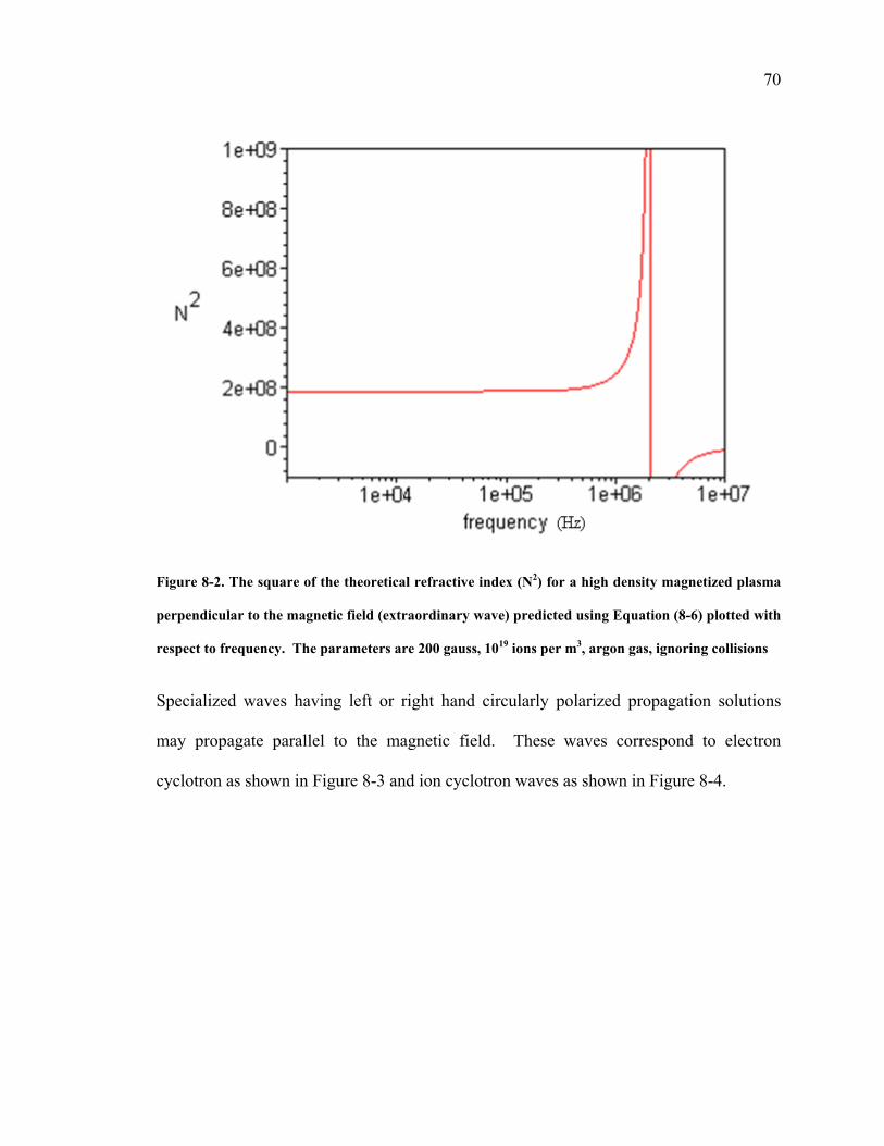
70
Figure 8-2. The square of the theoretical refractive index (N2) for a high density magnetized plasma
perpendicular to the magnetic field (extraordinary wave) predicted using Equation (8-6) plotted with
respect to frequency. The parameters are 200 gauss, 1019 ions per m3, argon gas, ignoring collisions
Specialized waves having left or right hand circularly polarized propagation solutions
may propagate parallel to the magnetic field. These waves correspond to electron
cyclotron as shown in Figure 8-3 and ion cyclotron waves as shown in Figure 8-4.

71
Figure 8-3. The square of the refractive index (N2) plotted with respect to frequency for special right
handed polarization propagation parallel to the magnetic field. Resonance occurs around 108 Hz
(not shown). The parameters are 200 gauss, 1019 ions per m3, argon gas, ignoring collisions.

72
Figure 8-4. The square of the refractive index (N2) plotted with respect to frequency for special left
handed polarization propagation parallel to the magnetic field. Resonance occurs around 104 Hz.
The parameters are 200 gauss, 1019 ions per m3, argon gas, ignoring collisions.
8.2.2 Geometry based frequencies
Another frequency that may be likely to appear would be the frequency of the drift
current around the magnetron erosion track. Published drift velocities range from (0.2 to
4.0) x104 m/s for HiPIMS which would result in a drift current frequency for a 150mm
cathode (estimating a 127mm diameter erosion track) between 5 and 100 kHz (79).
It would be logical for the plasma to oscillate from the charge imbalances at one and
perhaps all of its resonant frequencies. The velocity of the plasmoid and the strength of
the magnetic field are likely factors in the resulting observed frequencies (28).

73
In order to discuss the concept of assuming the uniformity of the plasma, it is useful to
consider the circular cathode depicted in Figure 8-5. As an electric field is applied to the
cathode, containing a ring of uniform plasma, the electrons will move away from the
cathode following the magnetic field lines of the magnetron cathode. Basic magnetron
designs have field lines that go out radially from the center to the outside of the
magnetron. Consider a system that starts with a perfectly uniform ring of high density
plasma as depicted within Figure 8-5 (a). Looking at the behavior of a small angular
section of the plasma over time, electrons within this angular section will have an inner
region that will move toward the outside, and an outer region that will move toward the
inside.
Figure 8-5. The change in the configuration of the plasma from a uniform plasma density to a non-
uniform plasma density, due to circular geometry. a) The first section shows an initially uniform
plasma density, with a small region ∆ marked, and b) then the electrons move in their cyclotron
path, resulting in c) the regions subtended in part “a)” switching places, generating a plasma density
fluctuation, not previously present. The plasma density change will result in an outward pressure
gradient .
e-
c)
b)
a)
∆

74
The electron density that was originally constant must now have an imbalance as the
volume enclosed in the outer portion of the ring is greater than the volume on the inside.
The motion by the electrons as they “hop” around the cathode inevitably results in a
plasma density variation in a circular cathode. Secondarily, an increase in pressure to a
smaller radius may be expected to result in an outward force from a pressure gradient.
This force in turn should move the high density plasma to a larger radius than may be
expected without consideration of the plasma as a fluid.
The plasma drift velocity in conjunction with the magnetic field and density gradient also
result in the possibility of drift waves within the plasma. These drift waves or other
waves are expected to inevitably develop in the plasma (28) (75). A schematic of these
oscillations is shown in Figure 8-6. The magnetic field lines come out of the plane at the
center of the cathode and arc back into the cathode on the outside ring (the “x’s” in the
schematic). The plasma density “wave fronts” are represented by the shaded area. The
wave fronts would likely continue to follow the arcing field lines.
Figure 8-6. A possible oscillation that can develop alongside the pressure gradient and drift within
the magnetic trap is schematically drawn (75).
Vdrift

75
8.2.3 Frequency matching
Through a process called frequency matching, any number of wave propagation
possibilities are opened up. Frequency matching is the excitation of a pair of waves from
an original higher frequency wave (75). Provided momentum is conserved two new
waves may be generated replacing the original wave. This provides a mechanism for
developing waves at various allowed frequencies.
8.3 Summary
In order to develop tools to understand the plasma and its interactions with waves, one
needs to look at the underlying equations and physics related to the plasma. Through this
equation analysis, conceptual models have been developed to understand the plasma
behavior.
Perpendicular to the magnetic field, depictions of the plasma behavior may be developed
to include the effects of ions, collisions and geometry, and may be further described
through the two-stream instability or the modified two stream instability theories.
Regardless of the model used, the dielectric constant remains large and positive for the
perpendicular direction over a large band of frequencies, indicating a capacitive effect.
The oscillations present may be of both electromagnetic waves and ionic sound waves.
These waves have characteristic cutoff and resonance frequencies within the plasma.
Key frequencies of note are the plasma frequencies and the cyclotron frequencies.

76
In general for the analysis there are minimally two species, argon ions and electrons,
resulting in four basic frequencies within the plasma. These frequencies increase with
increasing plasma density, and increase with increasing magnetic field for both plasma
and cyclotron frequencies. The analysis of these magnetized plasma equations results in
finding that 1) there is the possibility for wave propagation perpendicular to the magnetic
field within the plasma; 2) wave frequencies depend on plasma density and magnetic
field magnitude; and 3) the dielectric constant of the plasma may be large and positive
perpendicular to the magnetic field. Thus looking at wave propagation within a plasma is
one tool that can be used to understand plasma behavior.

77
Chapter 9 Case Study: Analysis of Prior Magnetron Models
Particle in cell models (PIC), like the plasma frequencies discussed last chapter, have also
become an important tool in the development of the understanding of how a magnetron
sputtering cathode will function. Goree and Sheridan were two early adapters of this
technique and brought a new level of understanding of the plasma’s behavior (31). Their
modeling was driven by an attempt to divulge an understanding of what caused the
transport of electrons across the magnetic field boundaries within plasmas, which at the
time was considered to be the result of plasma turbulent oscillations (28) (74).
9.1 Oscillations in Magnetron Plasmas
Sheridan et al. attempted to discredit the likelihood of oscillations contributing to the
conductivity of the plasma in several ways (28) (29) (30) (33). First, Sheridan and Goree
performed experiments at low sputtering intensities and analyzed the oscillations below
1MHz, concluding that these waves could not contribute to the current carrying of the dc
supplied power as ionic sound waves (28). Second, Sheridan et al. found that any
relationship described needs to follow a dependence on the mass of the gas (29). Third
Sheridan et al. attempted to demonstrate through particle-in-cell modeling that collisions
were an important factor in electron transport, and a more likely candidate than
oscillations for the current flow (31).
Sheridan et al. provide an excellent skeptical point of view and supplies a set of logical
requirements when looking for the mechanisms involved within current transport for a dc
magnetron. Sheridan and Goree discusses the concept of “τ” (tau), a time constant,

78
defining the confinement time of an electron in a plasma per equation (9-1) “τ” is defined
as proportional to the density of a plasma and inversely proportional to the current
flowing through the circuit. According to Sheridan and Goree “τ” may be described by
the equation:
(9-1)
where “e” is charge, N is total number of carriers in the plasma and Idis is the discharge
current of the magnetron. This variation is developed by acknowledging “ ” may be
replaced with “ ”. This provides a quick look at how fast the electrons within the
plasma must be replaced in order to maintain a steady state current flow.
Sheridan and Goree, then recognize that the low frequency waves are likely to be ionic
sound waves, and assume electrostatic ionic sound waves which may be described by:
(9-2)
However, in the case of Sheridan, the ions are assumed to be cold in comparison to the
electrons, and due to geometry constraints, the forces generating the minor deflections to
the ions from the magnetic field are ignored. Provided the frequency does not begin to
approach the ion plasma frequency, the “ ” term may also be ignored. These three
developments allow the simplification to the ion acoustic wave:
(9-3) ,

79
where is the ion acoustic wave speed. By combining the expected dispersion relation
of (9-3) with: a linearization of the Boltzmann relation per equation (7-14) for
a time varying potential; and a time varying electric field per equation (7-3); Sheridan et
al. developed (28):
(9-4)
The inverse of the time constant provides a zeroth order understanding for oscillations to
contribute. In order for a single wavelength to single handedly carry all the charge, the
frequency would be required to be greater than the inverse of the confinement time “τ”.
If the current in the magnetron is to be aided by the plasma’s oscillations the total amount
of flux transferred by each frequency measured within the plasma must be summed
across all possible frequencies. Sheridan invokes Parseval’s theorem to perform this
calculation finding the contribution at each given frequency as a method to find the total
power carried by the waves. Parseval’s theorem equates the power in the time domain to
the power in the frequency domain. One caveat to this calculation is that it assumes the
integration over the entire frequency spectrum, only a portion of which is available to
Goree and Sheridan.
Goree and Sheridan used a cylindrical Langmuir probe oriented parallel to the radial axis
of the magnetron for measuring the characteristics of the plasma. Plasma densities were
found in numerous positions within the system for finding the total N of the system. The
oscillations were measured at two positions within the plasma, both at 6.8 mm from the
face of the cathode, one nearly at the point where the magnetic field is parallel to the face
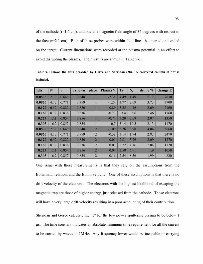
80
of the cathode (r=1.6 cm), and one at a magnetic field angle of 34 degrees with respect to
the face (r=2.1 cm). Both of these probes were within field lines that started and ended
on the target. Current fluctuations were recorded at the plasma potential in an effort to
avoid disrupting the plasma. Their results are shown in Table 9-1.
Table 9-1 Shows the data provided by Goree and Sheridan (28). A corrected column of “τ” is
included.
Idis N τ τ shown place Plasma V Te Ne del ne % change E
0.0536 2.17 0.649 0.648 1 -2.38 4.49 1.49 5.12 76300.0856 4.12 0.771 0.759 1 -1.24 3.77 2.69 3.73 3700
0.127 6.52 0.822 0.826 1 -0.89 3.55 4.16 2.69 21600.168 8.77 0.836 0.836 1 -0.73 3.4 5.6 2.46 17600.227 12.1 0.854 0.856 1 -0.74 3.29 7.69 2.07 13500.303 16.2 0.857 0.854 1 -0.7 3.14 10.5 2.13 1170
0.0536 2.17 0.649 0.648 2 -1.09 3.76 0.98 4.04 56600.0856 4.12 0.771 0.759 2 -0.38 3.14 1.94 2.82 2470
0.127 6.52 0.822 0.826 2 -0.01 2.81 3.26 2.09 12700.168 8.77 0.836 0.836 2 0.03 2.72 4.16 2.04 11200.227 12.1 0.854 0.856 2 0.04 2.59 6.01 1.9 10500.303 16.2 0.857 0.854 2 -0.16 2.54 8.56 1.99 820
One issue with these measurements is that they rely on the assumptions from the
Boltzmann relation, and the Bohm velocity. One of these assumptions is that there is no
drift velocity of the electrons. The electrons with the highest likelihood of escaping the
magnetic trap are those of higher energy, just released from the cathode. Those electrons
will have a very large drift velocity resulting in a poor accounting of their contribution.
Sheridan and Goree calculate the “τ” for the low power sputtering plasma to be below 1
µs. The time constant indicates an absolute minimum time requirement for all the current
to be carried by waves to 1MHz. Any frequency lower would be incapable of carrying
81
enough current, even if every available free electron contributes. Other groups had
indicated higher frequency oscillations at higher plasma powers (26); the intent of
Sheridan and Goree’s paper however was consideration of low frequency contributions.
Sheridan and Goree removed all high frequencies above 2.5 MHz with a highpass filter to
prevent aliasing and only consider measurements below 1MHz to avoid calculations
close to the plasma ion frequency (analyzing just a portion of the frequency domain).
Sheridan and Goree, therefore, have indicated that only oscillations with frequencies
above 1MHz will significantly contribute to the current, but then go on to measure only
frequencies below 1MHz. In effect, Sheridan and Goree measured for fluctuations in a
plasma whose density is so low that oscillations containing the entire group of available
charged particles within the plasma would not be enough to carry the current at the
frequencies the system is set up to measure.
Sheridan then demonstrates that the oscillations fail to follow the expected electric field
behavior by assuming the oscillations measured within the plasma are unmagnetized
ionic sound waves and analyzing their behavior. In the true sense of the term, the ions
are unmagnetized, due to the geometry of the system. However, their data suggests a
strong resonance at the ion cyclotron frequency. The dispersion relation of (9-3) for the
ionic sound wave approximation then begins to fail right where the frequency variation is
greatest.
The original dispersion equation of (9-2) results in a reduced dependence of the wave
number on frequency. Given a reduced dependence on frequency for wave number, the
electric field will no longer be strongly dependent on frequency, making the analysis of
82
the electric field from the base ion acoustic waves not as useful. Sheridan points out that
his experimental data lacks the required dependence on electric field with respect to “τ”
for the portion of the frequency domain experimentally analyzed using the simple ion
acoustic wave approximation. Without this dependence, he concludes the oscillations
present are not contributing to the current.
This conclusion however hinges on equation (9-3) which at low frequencies approaches a
lower limit at the ion cyclotron frequency and an upper limit at the plasma ion frequency.
At these limits the frequencies’ dependence on wave number is reduced and equation (9-
3) no longer accurately describes the dispersion relation. At these limits, frequency has a
reduced impact on the electric field calculations. Further complicating matters is
Sheridan’s attempt to divulge the electric field effects from the current measurements. A
more accurate way would be to use a direct measurement of the field which is the method
used by Martines (35).
This conclusion also relies on a uniform global “τ” applicable throughout the plasma
which would only be the case if the density uniformly changes with power applied. This
may be the case for position 1, but for position 2, (see Table 9-1) there is a secondary
dependence for local plasma density vs. total density. Figure 9-1 shows the behavior of
the local density in Sheridan’s magnetron system with respect to the local density divided
by the total number of ions Sheridan calculated within the plasma. The behavior is
different in the two places Sheridan et al. measured. In the first position which had a
higher magnetic field, which was also more perpendicular to the electric field, the relative
plasma density actually decreases. For the second region that contains a less

83
perpendicular field and lower magnetic fields, the measured relative density increases
with increasing global plasma density. Experimentally this makes good physical sense.
When a magnetron is operated at lower plasma densities, the region of high density
plasma is smaller, and at higher operating powers, the region of the higher density plasma
increases. This may also be evident in the erosion of targets.
Figure 9-1. The dependence of electron density with respect to electron density divided by the total
number of charge carriers. This plot allows the establishment of variable dependence. The power
value of “-.031” indicates a small dependence, with the relative local density decreasing as the total
plasma density increases. The power value of “.0626” indicates a small dependence, with the relative
density increasing as the total plasma density increases.
Numerically this may be understood in two separate ways, first similar to basic dc diode
behavior, the dc magnetron will have a “Paschen curve” for a given gas, pressure and
material (22) (80). A second way to reason the increased high density plasma region is
through the increased cathode fall voltage needed to maintain the plasma at the higher
y = 0.68x‐0.031
y = 0.45x0.063
0.4
0.45
0.5
0.55
0.6
0.65
0.7
0.75
0 2 4 6 8 10 12
Normalized
Den
sity
electron density
Ne/N Pos 1
Ne/N Pos 2
(ne)

84
currents. Sheridan starts at 350 V and ends at 550V for the voltage applied to the
cathode. This higher voltage results in a larger Larmor radius for the electrons emitted
from the cathode. The energetic electron gyroradius may be expected to follow the
following equation (22):
(9-1)
The Larmor radius is expected to determine the magnetic field line that the electron
becomes trapped upon, the larger the Larmor radius, the higher up the electron gets, and
the wider path the electron takes near the surface of the target.
Figure 9-2. The electrons move along lines of flux above the target. The width w of the track
followed by the electrons is in part due to the gyroradius for the electron. Higher voltage electrons
(grey) will have larger width erosion tracks. Schematic drawn after Liebermann and Lichtenberg
(22).
Finally, Sheridan’s work depends on the assumption that the waves are of the ion
acoustic type. Although possible, there are other modes available to the plasma in this
region including electromagnetic waves such as the left hand polarized electromagnetic
e- e-
w

85
wave. In fact there could be expected three separate electromagnetic waves within the
plasma, in the range of 0.1 to 1MHz.
The three possible wave types are the extraordinary, left hand polarized, and right hand
polarized waves. Previously these waves were plotted for the HiPIMS characteristics in
Chapter 8; the waves will again be plotted here with the parameters of Sheridan and
Goree. The right hand polarized wave as shown in Figure 9-3 begins to roll off near 104
Hz. Similarly, Sheridan and Goree’s data trails off as their data approaches the
megahertz region.
Figure 9-3. The the square of the refractive index (N2) vs. frequency (f) in Hz for the right hand
polarized wave, as known as the whistler mode. The values for this calculation were 1016 m-3 density,
argon gas and 132 Gauss magnetic field.

86
Sheridan and Goree also indicate a large spike near the ion cyclotron frequency, which
for the left hand polarized wave is a resonance, as may be seen in Figure 9-5.
Figure 9-4. Goree and Sheridan's observed frequency spectrum for variation in density (28). The
graph shows a normalized plot of the fluctuation in density with respect to the frequency of the
fluctuation.
The left hand polarized wave as shown in Figure 9-5 has a resonance around 8 kHz,
below which, the dielectric constant is large and positive. The LH wave is cutoff after
resonance and remains cutoff until nearly the plasma frequency well above 10 MHz.

87
Figure 9-5. The frequency (f) in Hz vs. the square of the refractive index (N2) for the left hand
polarized wave is graphed. The values for this calculation were 1016 m-3 density, argon gas and 132
Gauss magnetic field.
The extraordinary wave (defined as a wave propagating perpendicular to the magnetic
field) is shown in Figure 9-6 to have a large and positive dielectric constant over the
entire measured region until the lower hybrid resonance where the waves cuts off at just
over 106 Hz. The large positive dielectric constants for the waves in Figures 9-3, 9-5 and
9-6 indicate that the extraordinary wave may be capable of carrying power within the
plasma in the range analyzed by Sheridan and Goree.

88
Figure 9-6. The frequency (f) in Hz vs. the square of the refractive index (N2) for the extraordinary
wave is graphed. The values for this calculation were 1016 m-3 density, argon gas and 132 Gauss
magnetic field.
Although Sheridan’s own measurements tend to contradict a uniform change in plasma
density; this paper nonetheless clearly shows the difficulty lower frequencies would have
in carrying all the current. This paper thus sets forth the need for, at minimum,
contributions from other sources such as collisions or higher frequencies.
Sheridan’s discussion of low frequency waves is further narrowed to observe only self-
induced oscillations within the plasma and does not include any frequencies that may be
applied to the plasma in an attempt to drive a given frequency. Sheridan and Goree

89
indicate experiments were performed in driving the plasma at low frequencies. The data
Sheridan and Goree collected for the low frequency driven plasma was so different with
large variations in density that they concluded this behavior had to be a different
phenomenon then those oscillations present naturally and thus they did not include those
results (28).
9.2 Collisional Model and Particle in Cell
Goree and Sheridan then developed a particle-in-cell simulation of electrons escaping the
surface of a magnetron and tracked their movements (31) (32). 2-d simulations were
carried out with and without collisions. This model uses predetermined static electric and
magnetic fields. Initially electrons are released from the cathode surface to develop an
electron distribution near the cathode. This new electron distribution is then used to
formulate the probability of where to release electrons for the collision simulation. The
final result roughly represents a profile similar to the erosion track profile. The electrons
released during their model produced on average 3-4 excitation collisions, 48-49 elastic
collisions, and 20 ionization collisions. The time step for the system was 50ps and an
electron on average had a collision once every 130 time steps. The average electron
therefore was tracked for a total of 0.470 µs. This time constant is low in total time,
however, electrons were also ignored after 2.5 µs, providing an upper limit to the time
constant.
A more telling result is that the average number of ionizations was 14.26 which is larger
than the expected number of collisions. This result indicates that more electrons are

90
being generated, and confined for longer than they should. For a self consistent model,
the ionization rate of argon atoms from the electrons should equal the secondary electron
emission coefficient. Without equality, either the plasma is incapable of being sustained,
or the current should end up in runaway as the plasma density skyrockets. Sheridan and
Goree also show that for 600 electrons, about 200 electrons ionize 20 or more times.
These electrons no longer have the energy to escape the trap.
Their model also relatively well predicts the expected erosion track of the cathode. The
actual erosion track profile is slightly farther out in radial distance in comparison to the
modeled ionization events. This discrepancy is likely due to the modeling as a single
particle, in a static electric field. This model is not sensitive to pressure gradients, and
the electrons as they move inward will effectively increase in pressure, in comparison to
their maximum radial position.
9.3 Conclusions
Although the goal was to prove collisions were solely responsible for enabling electrons
to escape the magnetic field of the target, the conclusion was that most collisions are
small angle scattering events. The Sheridan and Goree model finds that significant
numbers of the electrons fully use up their energy ionizing argon, indicating the excellent
efficiency of a magnetron. Nearly one third of the electrons were tracked for the full 2.5
microsecond time allotment. If the particle-in-cell model was an accurate depiction of
events, the result would be a buildup of spent electrons within the magnetic trap.

91
A buildup in electrons within the magnetic trap would effectively screen the cathode
from the plasma and reduce/remove the cathode fall’s electric field. The potential drop
would be forced to be diverted across the whole of the plasma. Clearly this does not
occur, nor would it make sense. The other behavior that might occur is current run
away. If each electron ejected creates more ions than are needed for a balanced
magnetron, then the current will simply continue to increase. The picture thus created
would be a decreasing cathode fall voltage with increasing current. The model therefore,
does not appear to be charge/current flow balanced. Ideally each electron would be
tracked until the electron finds a wall or is otherwise neutralized. Clearly there is still a
need to describe the traversal flow of electrons across magnetic field lines beyond the
expectations derived from following single electrons. One possible method used by some
is a circuit equivalent model (21) (76).

92
Chapter 10 Plasma circuit equivalent model
In previous chapters the dielectric constants of the plasma were described in the parallel
and perpendicular direction to the magnetic field. Perpendicular, the dielectric constant is
large and positive; parallel to the magnetic field, the dielectric constant is large and
negative. So, in effect, a magnetic plasma behaves as a semi-infinite network of
inductors and capacitor;, a simplified view of the network is depicted in Figure 10-1 (81).
N N S
Figure 10-1. An illustration of the magnetron plasma represented as a series of capacitors and
inductors; resistive components have been removed for clarity.
Figure 10-1 is a sketch of an electrical analogy for a magnetron plasma and shows the
capacitive behavior perpendicular to the magnetic field lines, and the inductive behavior
along field lines. This concept may be further evaluated by applying the above equations
in a dielectric constant tensor to evaluate propagation through the plasma as developed in
chapter Chapter 1 and applied in chapter Chapter 8 (22).

93
10.1 Magnetron circuit
Noting that the plasma can act as a network of inductors and capacitors is interesting, but
more interesting is what effects this may have on the expected plasma behavior locally,
and overall on the plasma current-voltage characteristics for DC and HIPiMS processes.
In order to more easily evaluate various effects on the plasma model, a simplified version
using individual RLC components in Matlab’s Simulink software is used. The power
supply was modeled as a capacitor discharging into the plasma as shown in Figure 10-2
a); and in Figure 10-2 b) the inductor capacitor network depicted in Figure 10-1 is
schematically drawn. The number of elements used in Figure 10-2 was chosen as the
minimal number needed to accomplish the development of every possible connection that
may be expected using the inductance/capacitance relationship for a magnetized plasma.

94
Figure 10-2. The model for the power supply (a), and the model for the plasma (b) is schematically
depicted. A capacitor set is shown for both sheaths. The flux lines are modeled as inductors parallel
and capacitors perpendicular to the plasma. The flux lines that are modeled are overlaid as dotted
grey lines.
a)
b) Sheath Sheath Flux lines

95
The viability of the HiPIMS supply model was tested through a resistor first, and then
through the plasma model. Figure 10-3 shows the current (dashed lines) and the voltage
(solid lines) through both a resistor and through the plasma network.
Figure 10-3. The Current and Voltage vs. time curve for the power supply through a resistive load (
grey dashed lines) and the I and V vs. t curve for the plasma model without resistive variation (solid
lines).
The capacitance of the network absorbs some of the energy output by the supply as
illustrated by the voltage dropping quicker initially. At the end of the pulse this
capacitance slowly reduces the target voltage in comparison to the resistor. No ringing
was observed. No oscillations grew during the pulse. An initially large drop in voltage
was not observed. The magnetron model consists completely of passive elements, and
-1000
-900
-800
-700
-600
-500
-400
-300
-200
-100
0
0 0.001 0.002 0.003 0.004 0.005
time (s)
Volta
ge (V
)
-100
-90
-80
-70
-60
-50
-40
-30
-20
-10
0
Cur
rent
(A)

96
fails to create by itself any significant ripples within the current or voltage curves. This
model is still in need of mechanisms to generate the oscillations. Possible adjustments
could be; exchanging the resistive component of the sheath for a diode, more elements
generating a 3-d picture rather than the 2-d simulation shown, and simulating the inherent
oscillations within the plasma by directly varying a passive element to simulate the
expected turbulence within the plasma. This third concept is explored next.
10.2 Turbulence effect
In order for the capacitive portion of the plasma to make a contribution to the conduction
of current, a portion of the current must be carried as a wave. dc magnetron sputtering is
known to have rf fluctuations within the plasma (27) (28) (35) (74). Since the only
power source within the magnetron plasma is the cathode we do not necessarily want to
simply add a varying power supply. We know through the body of work performed in
sputtering plasmas and discussed in chapter 9 that plasma densities will oscillate. This
model allows a variation in plasma density to be represented as a change in local
resistance within the plasma. The total resistance will be kept constant by varying
another region of the plasma out of phase with the first. A switch will be implemented
that varies the resistivity locally in the plasma network. The switch results in zero net
change in dc resistivity through timing with other switches in the network. In an effort to
analyze the current carrying capability, we will simplify the network circuit as shown in
Figure 10-4 and described below.

97
Figure 10-4. The simplified network with a pair of choppers (modulated resistivity) used to simulate
the plasma as a pair of capacitors with parallel resistors to conduct the power.
In this model the HiPIMS supply has been replaced by a simple dc supply. The plasma
has been reduced to a pair of pathways each containing a capacitor on each end
representing the sheaths, and a pair of parallel resistors for the plasma. The resistors are
modulated between a resistance of 100 and 1 Ω at the frequencies of 1 Hz and 10 kHz.
The paths through the resistors are set up such that when one switch opens, the switch on
the other path closes, and to insure there is no time spent with both on, the array is set
with a 45% duty cycle, providing a brief time with both resistors out of the circuit
resulting in an overall increase in resistance of the circuit over time. The dc resistance of
the entire circuit is about 18 Ω, and the resistance during oscillations is approximately 18
Ω 90% of the time and 60 Ω 10% of the time. The resistance, capacitance of the system
and system frequency has been arbitrarily selected for demonstration purposes.

98
Figure 10-5. The dc behavior for Voltage and RMS current supplied to the cathode as depicted by a
simplified power system model is graphed as current vs. time. The upper line operates the chopper
circuit at 10 kHz, and the lower line is at 1Hz.
Initially the system is operated with the switches alternating at a time greater than the
analysis time (1 Hz) to approximate a dc signal. As seen in Figure 10-5, after the initial
charging of the capacitors within the circuit, the current reaches a steady state value of 56
A. This is in-line with the expected current from adding up the resistances of the simple
circuit. The voltage for both cases remains nearly steady at the applied value of 1000 V.
By setting a higher frequency for the switching, the current passing through the system
increases and doubles to 112 A in the steady state, indicating the possibility of a
mechanism by which the capacitive effect of the plasma perpendicular to the target
voltage may result in a lower resistance for an applied dc input. One such mechanism
would be any changing plasma density over time at a fixed position within the plasma.
0
50
100
150
200
250
0 0.0005 0.001 0.0015 0.002
time (s)
Cur
rent
(A)
Current with chopper at 10kHz
Current with chopper at 1Hz

99
This chopper mechanism may be considered an approximation of any number of
measured waves found by other groups (27) (28) (74) for magnetron plasmas. For
example, a likely source would be a diocotron type wave developed within the E×B drift
current above the cathode as described by Thornton (23). For simplicity the network was
setup with just two branches, however, it is entirely likely that the magnetron has
multiple regions of variations of plasma density over the surface of the target providing
the system with multiple switching possibilities.
10.3 Conclusions
A model for predicting the behavior of magnetron plasmas has been described. A
mechanism by which the magnetized plasma may contribute to dc conductivity in wave
form has been introduced and demonstrated using electrical circuit equivalents. This lays
the groundwork for better modeling of the magnetron plasma through electrical
equivalents and through finite element modeling. The model shows that it is possible to
generate an improved current through the density variations known to exist within
plasmas (27) (35) (82) (83). Variations of the type developed within this model,
however, fail to show a variation or amplification of an oscillation in the applied voltage
and output current like those that have been experimentally observed in HiPIMS plasmas
(8) (71). The oscillations presented are local oscillations; their presence reduces the
effective resistivity of the system, but they do not cause global ripples. The global
oscillations, therefore, must affect an entire region of the plasma. The most logical place
left to look is at the sheath, and at our own data.

100
Chapter 11 Experimental Data
The experimental data was collected on two separate systems. One system was in
Linköping Sweden; the other system was at University of Nebraska-Lincoln (UNL).
Data was collected over a range of material targets in both systems.
11.1 Experimental Setups
The two experimental setups have slight variations in comparison to each other,
particularly in chamber geometry and magnet configuration. The UNL system is
designed for controlled unbalanced sputtering, and includes a coil behind the substrate.
11.1.1 The “Maggie” Chamber
The UNL system (as shown in Figure 11-1) consists of a 150 mm nearly balanced Sierra
Applied Sciences “high material utilization” cathode, a coil to provide greater
unbalancing and magnetic field at the target, and a 44 wavelength ellipsometer mounted
at 66 degrees relative to the substrate plane. Figure 11-2 shows the typical magnetic field
strengths and orientation inside the chamber due to the magnetron cathode. The 50mm
substrates were positioned approximately 150mm away from the target surface, and the
chamber is pumped by a turbopump to achieve a base pressure on the order of 1x10⁻⁷ torr.
A 100 turn coil is positioned 200mm away from the cathode behind the substrate and
may be supplied with up to 5 amps generating a field of 50 gauss at the substrate.

101
Substrate
Coil
Target
Ellipsometer
Figure 11-1. A schematic diagram of the magnetron sputtering system at UNL “Maggie”.
Figure 11-2. A confirmed model of the magnetic field direction, and strength of the "maggie
chamber". The contour lines represent magnetic field strength of 10 gauss increments, and the
arrows indicate magnetic field direction.

102
All runs were carried out by first setting the coil to an appropriate current (0-5 amps).
Next the chamber was backfilled to a pressure of one to five mTorr with argon gas, and
the Chemfilt Sinex 1.2 HiPIMS power supply was set to the desired voltage. The
HiPIMS power supply consisted of 10µF capacitor bank that may be charged to a
maximum of 2kV; thus generating pulses in excess of 1 MW peak power at a frequency
of 60Hz. These pulses have an initial current peak on the order of 200 microseconds
followed by a variable secondary peak whose timescale depends on the target material
and may approach 1/60 s.
A Tektronix P6015 high voltage probe measured the target voltage, while the current was
measured with a Tektronix TCP202 ac/dc current probe. At larger currents a Tektronix
CT-04 high current transformer together with a Tektronix TCP202 current probe were
used. The probe current, target voltage and target current were monitored and recorded
using a Tektronix TDS 520C oscilloscope.
11.1.2 Linköping University chamber
The Linköping University (LiU) chamber consisted of a vacuum system composed of a
cylindrical vacuum chamber (height 70cm, diameter 44cm) with a turbo-molecular pump
delivering background pressures between 10-6 and 10-8 Torr (schematic is shown in
Figure 11-3). Inert gas pressures in the range of 2 to 20 mTorr were backfilled into the
chamber; then a plasma was ignited using a HiPIMS supply as described below.

103
Figure 11-3. Schematic Diagram of the Swedish HiPIMS system. Courtesy Johan Böhlmark, Chemfilt
Ionsputtering AB
A circular planar magnetron (magnetic field schematic shown in Figure 11-4) equipped
with either a 150-mm chromium or aluminum target was used for the experiments. In
both cases short high voltage pulses were applied between the cathode/target material and
the chamber walls. The power supply used is a Sinex 1 manufactured by Chemfilt
Ionsputtering AB, Sweden. The Sinex 1 is able to deliver 2400 V and 1200 A peak values
with pulse duration lengths of approximately 100 µs with a repetition frequency of 50 Hz,
and is delivered by a 13.5 μF capacitor bank.
A Tektronix P6015 high voltage probe measured the target voltage, while the current was
measured with a Tektronix CT-04 high current transformer together with a Tektronix
TCP202 current probe. The probe current, target voltage and target current were
monitored and recorded using a Tektronix TDS 520C oscilloscope.
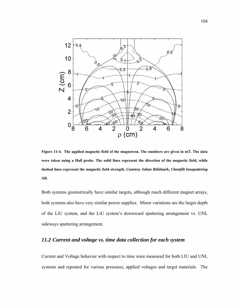
104
Figure 11-4. The applied magnetic field of the magnetron. The numbers are given in mT. The data
were taken using a Hall probe. The solid lines represent the direction of the magnetic field, while
dashed lines represent the magnetic field strength. Courtesy Johan Böhlmark, Chemfilt Ionsputtering
AB.
Both systems geometrically have similar targets, although much different magnet arrays,
both systems also have very similar power supplies. Minor variations are the larger depth
of the LiU system, and the LiU system’s downward sputtering arrangement vs. UNL
sideways sputtering arrangement.
11.2 Current and voltage vs. time data collection for each system
Current and Voltage behavior with respect to time were measured for both LIU and UNL
systems and repeated for various pressures, applied voltages and target materials. The

105
voltage range evaluated was between 500-1600V, since below 500V the current was low,
and above 1600V the plasma becomes unstable. A full set of data may be found in the
Appendices. Appendix A is the UNL data, and Appendix B is the LIU data.
Since HiPIMS generators, and the definition of HiPIMS covers a wide range of pulsed
systems, HiPIMS results appear to vary from system to system. These variation may
occur due to magnetic, grounding, stray inductances and capacitances as well as design
differences.
A typical discharge curve found in the UNL “Maggie” chamber is shown in Figure 11-5
with the same time scale for the Linköping system. The curves shown for the UNL
system are for an argon gas pressure of 3mTorr, at an applied voltage of 1144 Volts on a
titanium target, the UNL data may be found in Appendix A. The data in the appendix
will not look like Figure 11-5 but instead Figure 11-6.

106
0.0012 0.0013 0.0014 0.0015 0.0016
-1000
-500
0
Volta
ge (V
olts
)
time (s)
0.0012 0.0013 0.0014 0.0015 0.0016
0
5
10
15
Cur
rent
(Am
ps)
Figure 11-5. Typical discharge for UNL HiPIMS system, current and voltage for titanium at 3mTorr
of argon and 1144 Volts, scaled to a similar time frame to LiU data.
The data looks like Figure 11-6 because, in the process of taking the data in Linköping,
an improved data compression method was found and later used in the data collection at
UNL. This allowed for significantly more data points to be saved and transferred for a
single pulse. Figure 11-5 is a subset of the data presented in Figure 11-6 zooming in at
the large initial pulse.

107
0.000 0.005 0.010
-1000
-500
0
Vol
tage
(Vol
ts)
time (s)
0.000 0.005 0.010
0
5
10
15C
urre
nt (A
mps
)
Figure 11-6. Typical discharge for UNL HiPIMS system, current and voltage for titanium at 3mTorr
of argon, and 1144 Volts applied discharging to about 500 V.
A typical discharge curve acquired in a system in Linköping is shown in Figure 11-7, the
LIU data may be found in Appendix B.

108
0.0000 0.0001 0.0002-1000
-800
-600
-400
-200
0
Vol
tage
(Vol
ts)
time (s)
0.0000 0.0001 0.00020
20
40
60
80
100
Cur
rent
(Am
ps)
Figure 11-7. Typical discharge for Linköping system. Voltage applied to aluminum at 22.5 mTorr
starting at about 832 Volts initially applied, discharging to about 500 volts.
11.3 Physical data range
The characteristics of the HiPIMS plasmas have been collected on 2 systems, 5 elements,
several pressures, and one working gas, and a range of applied voltages. Table 11-1
indicates the expanse of experimental space reviewed.

109
Table 11-1. Materials and conditions selected for observing oscillations in HiPIMS.
Chamber Material AMU Gases (AMU)
Pressure (mTorr)
Applied Voltage
UNL copper 63.6 Ar(40) 3 750-1300V
titanium 47.9 Ar(40) 3 435-1330V
silver 108 Ar(40) 3, 5 300-1000V
LiU aluminum 27 Ar(40) 5-22.5 400-1700 V
chromium 52 Ar (40) 2-22.5 400-1700V
Each run has a number of characteristics that help describe the behavior of the system. In
order to further refine the analysis, the current vs. time and the voltage vs. time are also
important characteristics to further define the system.

110
11.4 Current and voltage vs. time for each element
The following curves (Figure 11-8 through Figure 11-11 are for various experiments run
on the UNL system. The first figure (Figure 11-8) is the current and voltage vs. time
graph trends for copper at 3 mTorr and 800 volts. A complete set of graphs may be
found within the appendix A.1 .
0.0000 0.0001 0.0002 0.0003 0.0004 0.0005
-800
-600
-400
-200
0
Volta
ge (V
olts
)
time (s)
0.0000 0.0001 0.0002 0.0003 0.0004 0.0005
0
4
8
Cur
rent
(Am
ps)
Figure 11-8. Current and voltage curves for copper at 3mTorr and 830 Volts initially applied.

111
The current and voltage vs. time graph trends for titanium at 3 mTorr and 800 volts are
shown in Figure 11-9 and no coil current. A complete set of graphs may be found within
the Appendix A.2
0.0003 0.0004 0.0005 0.0006 0.0007
-800
-600
-400
-200
0
Targ
et V
olta
ge (V
)
time (s)
0.0003 0.0004 0.0005 0.0006 0.0007
-20
-15
-10
-5
0
Targ
et C
urre
nt (A
)
Figure 11-9. Current and voltage characteristics for titanium at 820 Volts initially applied and
3mtorr with the coil off.

112
The current and voltage vs. time graph trends for titanium at 3 mTorr and 800 volts with
the coil on are shown in Figure 11-10 with a coil current of 5 amps. A complete set of
graphs may be found within the appendix A.2 .
0.0002 0.0004 0.0006 0.0008-900-800-700-600-500-400-300-200-100
0100
Targ
et V
olta
ge (V
)
time (s)
0.0002 0.0004 0.0006 0.0008
-16-14-12-10-8-6-4-202
Targ
et C
urre
nt (A
)
Figure 11-10. Current and voltage characteristics for titanium at an initially 820 Volts and 3mtorr
and a coil current of 5 amps.

113
The current and voltage vs. time graph trends for silver at 5 mTorr and 800 volts are
shown in Figure 11-11. A complete set of graphs may be found within the appendix A.3 .
The silver target failed to ignite at 3 mTorr without the coil on at 5 Amps.
0.004 0.006 0.008 0.010
-800
-600
-400
-200
0
Targ
et V
olta
ge (V
)
time (s)
0.004 0.006 0.008 0.010
-2
-1
0
Targ
et C
urre
nt (A
)
Figure 11-11. Current and voltage characteristics for silver at an initially applied 820 Volts and
5mtorr.

114
A characteristic current and voltage vs. time graph trend for aluminum (run on the LiU
system) at 5 mTorr is shown in Figure 11-12. A complete set of graphs may be found in
Appendix B.1
0.0000 0.0001 0.00020
20
40
60
80
100
Cur
rent
(Am
ps)
time (s)
0.0000 0.0001 0.0002
-800
-600
-400
-200
0
Volta
ge (V
otls
)
time (s)
Figure 11-12. Current and voltage curves for aluminum at 5 mTorr and 830 Volts initially applied.

115
A characteristic current and voltage vs. time graph for chromium (run on the LiU system)
at 5 mTorr and 800 volts is shown in Figure 11-13. A complete set of graphs for the
range of applied voltages and pressures may be found within Appendix B.2 .
0.0000 0.0001 0.0002-1000
-800
-600
-400
-200
0
Volta
ge (V
olts
)
time (s)
0.0000 0.0001 0.00020
20
40
60
80
100
Cur
rent
(Am
ps)
time (s)
Figure 11-13. Current and voltage curves for chromium at 5 mTorr and 830 Volts initially applied.

116
Chapter 12 Results and Discussion
The intent of this dissertation is to provide a better understanding of the HiPIMS process
by first analyzing the underlying physics, second developing a model of the process, and
third experimentally confirming the results and analyzing the differences between the
model and the experimental results. Within this dissertation, the previous chapters:
• provided motivation for using and understanding the HiPIMS process;
• outlined core plasma behaviors pertinent to magnetron sputtering;
• reviewed prior developments in magnetron sputtering; developed a basic circuit
equivalent model for the magnetron plasma; and
• experimentally generated current and voltage characteristic curves for materials of
aluminum, chromium, copper, silver, and titanium.
The unifying purpose for these sections was to identify the fluctuations that appear in
many HiPIMS processes. From this identification we hope to improve HiPIMS processes
in the future through industry acceptance and introducing other fields of study and their
body of work to HiPIMS processes.
First, the current and voltage characteristics for HiPIMS plasmas need to be discussed,
and the oscillations of interest identified. One particular point of interest is that the
oscillations may be present in either the voltage curve and/or the current curves. The
Linköping system tended to have the oscillations appear in the voltage, and the UNL
system tends to have the oscillations in the current (see Figure 12-1 and Figure 12-2 vs.
Figure 12-3). Variations in impedance from system to system due to any number of

117
variables, including length of power cable could contribute to where the oscillations
appear.
12.1 Current and Voltage Characteristics
A HiPIMS process starts with a high voltage pulse applied to a magnetron, and after a
small time delay, current begins to flow (See Figure 12-1, Figure 12-4, and Figure 12-5).
The delay time shortens slightly with increasing applied voltage.
0.0000 0.0002 0.0004 0.0006 0.0008 0.0010-600
-400
-200
0
Targ
et V
olta
ge (V
)
time (s)
0.0000 0.0002 0.0004 0.0006 0.0008 0.0010
-4
-3
-2
-1
0
Targ
et C
urre
nt (A
)
Figure 12-1. Titanium at 3mTorr with 550V applied. A clear lag (shaded region) between current
flow and voltage applied may be seen.

118
Once current begins to flow, the voltage drops and the current increases. An initially
sharp current spike is visible in Figure 12-2. The current develops into a sharp peak, and
then declines. After this sharp initial current spike, the current gradually increases a
second time. The second peak begins to overtake the initial peak in maximum current
with larger initially applied voltages. The larger voltage also indicates more total charge
available for the pulse. The second peak contains a number of small oscillations in the
current. These oscillations match up with the region of large voltage oscillations from
Linköping University’s HiPIMS system shown in Figure 12-3. The second peak is often
attributed to the metal ion dominated plasma (73). The oscillations do not occur for all
metals or all initial applied voltages.
0.000 0.002 0.004
-1000
-500
0
Vol
tage
(V)
time (s)
Ar ionvoltage drop
metal ion voltage drop
0.000 0.002 0.004
-10
-8
-6
-4
-2
Cur
rent
(A)
metal ion peakAr ionpeak
Figure 12-2. Titanium current and voltage curves at 1200V, a clear second region is present in the
current curve after the initial peak. Typically there is an initial current from the argon ions, and

119
then a second peak from the metal ions is detected. The current peaks have corresponding voltage
drops.
-0.00005 0.00000 0.00005 0.00010 0.00015 0.00020
-1800-1600-1400-1200-1000-800-600-400-200
0200
Vol
tage
(Vol
ts)
time (s)
metal ion voltage drop
Ar ion volt drop
-0.00005 0.00000 0.00005 0.00010 0.00015 0.00020
-1000
100200300400500600700
Cur
rent
(Am
ps)
time (s)
Figure 12-3. 5 mTorr aluminum at 1700V applied voltage indicating several behaviors present in
HiPIMS current and voltage curves. An initial voltage drop again is followed by a second voltage
drop. A periodic oscillation increases in frequency and amplitude during the discharge of the supply
overlaying the region of the second voltage drop.
Figure 12-3 does not have the corresponding peaks for the argon and metal ions in the
current. This is likely due to the method of acquiring the current (measuring the
magnetic field), and that the current occurs on a much more compressed timescale on the
Linköping University system which may contribute to the peaks overlapping.

120
12.1.1 Current and voltage curves for selected pulses
In order to provide an in-depth analysis of the voltage curves, chromium and aluminum
current and voltage graphs are compared. Figure 12-4 shows a series of the voltage
curves for chromium at 5mtorr and for initial voltages of approximately -1500V, -1250V,
-900V and -620V. Figure 12-5 for aluminum shows a series of curves similar to that of
Figure 12-4 for chromium. These graphs show higher starting voltages resulting in lower
final voltages in nearly the same discharge time. The graphs indicate the aluminum tends
to have higher current (through larger total voltage drops) and larger fluctuations than the
chromium.
Figure 12-4. Shows voltage vs. time for chromium at 5 mTorr for 600 through 1700 starting voltages.
(a) is 600 volts initially applied, (b) is 800 Volts initially applied (c) is 1100 Volts initially applied (d) is
1300 Volts initially applied and (e) is 1700 Volts initially applied.
-1800
-1600
-1400
-1200
-1000
-800
-600
-400
-200
0
0.00E+00 5.00E-05 1.00E-04 1.50E-04 2.00E-04time (s)
targ
et v
olta
ge (V
)
Cr 5mTorr
a
b
c
d
e
a,b
cd
e

121
Figure 12-5. Shows voltage vs. time for aluminum at 5 mTorr for 600 through 1500 starting voltages.
(a) is 600 volts initially applied, (b) is 900 Volts initially applied (c) is 1050 Volts initially applied (d) is
1250 Volts initially applied and (e) is 1500 Volts initially applied.
In the case of the present process for the Linköping system, higher initial voltages were
met with larger currents and faster discharge times. The resistance of the system drops
with applied voltage. The drop in the resistance of the system is expected as the HiPIMS
process attempts to follow the behavior of equation (8-1) since, the equation is non-linear
between current and voltage. In looking at the oscillations in the current voltage curves,
the oscillations get bigger with higher applied voltages. The oscillations also are material
-1800
-1600
-1400
-1200
-1000
-800
-600
-400
-200
0
0.0E+00 5.0E-05 1.0E-04 1.5E-04 2.0E-04time (s)
Vol
tage
(V)
Al 5mTorr
a
b
c
d
e
ab
cd
e

122
dependent. The largest oscillations occur for aluminum, which also has the highest
current of all the metals tested.
12.1.2 Maximum current vs. maximum voltage
The maximum current developed by the system varied with applied voltage and argon
pressure. A plot of the maximum current for chromium as a function of initial applied
voltage is shown in Figure 12-6.
Figure 12-6. A graph of peak applied voltage vs. peak developed current is plotted for various
pressures of argon. Error in the applied voltage measurement is +/- 10 Volts.
0
200
400
600
800
1000
1200
1400
1600
1800
1 10 100 1000
Current (A)
Volta
ge (V
)
2 mTorr5 mTorr10 mTorr15 mTorr20 mTorr
Cr
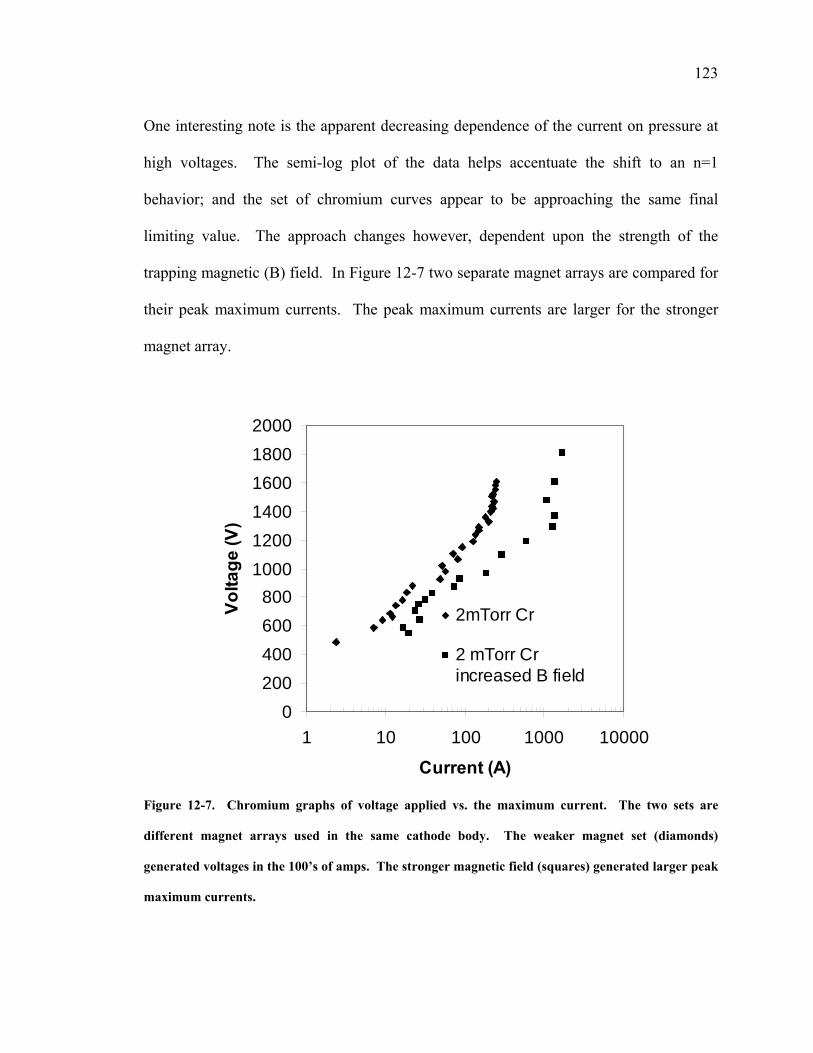
123
One interesting note is the apparent decreasing dependence of the current on pressure at
high voltages. The semi-log plot of the data helps accentuate the shift to an n=1
behavior; and the set of chromium curves appear to be approaching the same final
limiting value. The approach changes however, dependent upon the strength of the
trapping magnetic (B) field. In Figure 12-7 two separate magnet arrays are compared for
their peak maximum currents. The peak maximum currents are larger for the stronger
magnet array.
Figure 12-7. Chromium graphs of voltage applied vs. the maximum current. The two sets are
different magnet arrays used in the same cathode body. The weaker magnet set (diamonds)
generated voltages in the 100’s of amps. The stronger magnetic field (squares) generated larger peak
maximum currents.
0200400600800
100012001400160018002000
1 10 100 1000 10000
Current (A)
Volta
ge (V
)
2mTorr Cr
2 mTorr Crincreased B field

124
The pressure independence is not solely a behavior of chromium as the Figure 12-8
shows for aluminum at pressures of 2 and 20 mTorr. The transition in the current-voltage
curve is also not as pronounced for the aluminum.
Figure 12-8. Current maximum vs. maximum applied voltage for aluminum at both 5 and 20 mTorr.
The values appear to converge toward a single value.
12.2 Average Resistance vs. Applied Voltage
By using the Voltage vs. time curves and approximating the discharge time, as well as
initial and final voltages, an average resistance and current of the plasma may be obtained
0
200
400
600
800
1000
1200
1400
1600
1800
1 10 100 1000 10000
Current (A)
Volta
ge (V
)
5mTorr20 mTorr
Al

125
through fitting the data. An average resistance is developed through the following
capacitance discharge equation:
(12-1) ⎟⎠⎞
⎜⎝⎛ −
= RCt
c EeV or ⎟⎠⎞
⎜⎝⎛ −=⎟
⎠⎞
⎜⎝⎛
RCt
EVcln
where Vc is the current voltage of the capacitor, E is the initial voltage of the capacitor, t
is the elapsed time since discharging started, and R and C are the resistance and
capacitance of the system respectively. Using equation (12-1), and the 13.5 μF
capacitance of the power supply, the resistance for a -1500V pulse is determined to be 1-
2 ohms, and the resistance for a -700V pulse is about 45 ohms for aluminum. By finding
the average resistivity of the system over a number of applied voltages, the trends
illustrated in Figure 12-9 and Figure 12-10 are developed.

126
Figure 12-9. The resistance as a function of applied voltage for chromium at a range of pressures.
All the pressures appear to converge to one resistance at high applied voltages.
0
50
100
150
200
250
0 500 1000 1500 2000Voltage (V)
Res
ista
nce
(Ω)
2 mTorr5 mTorr10 mTorr15 mTorr20 mTorr
Cr
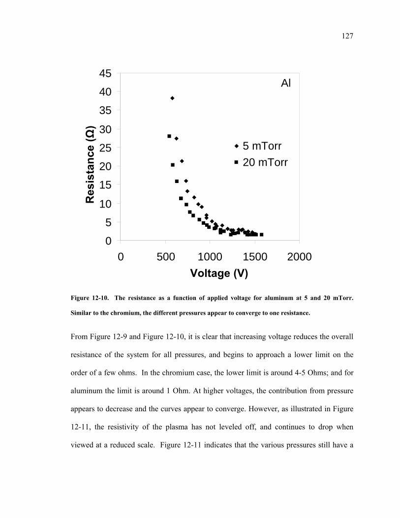
127
Figure 12-10. The resistance as a function of applied voltage for aluminum at 5 and 20 mTorr.
Similar to the chromium, the different pressures appear to converge to one resistance.
From Figure 12-9 and Figure 12-10, it is clear that increasing voltage reduces the overall
resistance of the system for all pressures, and begins to approach a lower limit on the
order of a few ohms. In the chromium case, the lower limit is around 4-5 Ohms; and for
aluminum the limit is around 1 Ohm. At higher voltages, the contribution from pressure
appears to decrease and the curves appear to converge. However, as illustrated in Figure
12-11, the resistivity of the plasma has not leveled off, and continues to drop when
viewed at a reduced scale. Figure 12-11 indicates that the various pressures still have a
0
5
10
15
20
25
30
35
40
45
0 500 1000 1500 2000
Voltage (V)
5 mTorr
20 mTorr
Al R
esis
tanc
e (Ω
)

128
small influence near the end of the explored voltage range indicating not a change in
behavior, but an approach to a non-zero asymptote.
Figure 12-11. The pressure and material dependence of the resistance from the plasma may be
observed through the voltage vs. resistance curve. The chromium data is in gray (triangles, asterisks,
bullets and plusses), and aluminum data is black (diamonds and squares). The scale of this graph has
been adjusted to have a non zero lower limit in order to see that the curve continues at the small
resistance values.
To test whether the magnetic trapping still has an affect at these high voltages, a newer
magnet array was installed. Figure 12-12 indicates the effect of an increased magnetic
field on the chromium target resistance behavior at 2mTorr. Increasing the magnetic
3
4
5
6
7
8
9
10
0 500 1000 1500 2000
Voltage (V)
Res
ista
nce
(Ω)
5 mTorr20 mTorr2 mTorr5 mTorr10 mTorr15 mTorr20 mTorr
Al
Cr

129
field extends the region where the current-voltage relationship follows the Equation (8-1)
power relationship until reaching a minimum resistance of approximately 1 ohm.
Figure 12-12. A new asymptotic approach for the minimum resistance in comparison to the original
magnet array for the same pressure may be seen in the figure. The lower magnetic field data set is
black squares. The larger magnetic field data set are dark circles. The increased B field achieves a
lower minimum resistance.
12.3 Modified magnetron I-V fit
In order to compare this data to the voltage-current relationship for magnetron sputtering,
the average current for each pulse was calculated from the change in target voltage. The
0
10
20
30
40
50
60
70
80
90
100
0 500 1000 1500 2000 Voltage (V)
Res
ista
nce
(Ω)
Increased B
standard B
Cr

130
initial voltage values for the pulse were then plotted with respect to the resulting average
current, as illustrated in Figure 12-6. As reported by others (84) (85) (86), the I-V
characteristics initially follow an “n” value for equation (8-1) between five and six. At
higher voltages, the curve transitions to an “n” value of approximately one. A single fit
may be made over the entire voltage regime by adding a second term to the voltage
characteristics of the magnetron. Thus, modifying the equation as:
(12-2) IRk
IVn
n+= 1
1
Where R is the resistance, and the IR term accounts for the n=1 contribution. The IR
term also accounts for the non-zero asymptote clearly visible when the data is plotted
with respect to resistivity in Figure 12-9 through Figure 12-12. The IR term may be
caused by several phenomena. First, the resistance and their associated voltage drops
between the measurement point and the target face may become significant at currents in
the range of hundreds of amps. Second, the system is not dc, and the cabling, and any
inductors included in the setup will oppose the rapidly increasing current. Finally, the IR
behavior can also result from the magnetron beginning to lose magnetic confinement as
proven by others previously (74).
Equation (12-2) fits the data over the entire measured voltage range. For example, in
Figure 12-13 the voltage is plotted with respect to current for chromium along with the fit
of equation (12-2) with n=6 and R=2 ohms; the individual terms are also graphed to
illustrate their contribution to the whole equation. Two ohms is much greater than the
expected resistance and resulting voltage drop across the cathode and target for chrome

131
and therefore this resistance is likely plasma based, such as an indication of a magnetic
field too weak to provide confinement. Figure 12-14 shows the I-V curve for the
aluminum fit using equation (12-2) with n=6 and R=0.5 ohms.
Figure 12-13. A fit to the current maximum vs.-applied voltage maximum curve by adding an "n=1"
term to the system for 15 mTorr chromium. The graph also helps demonstrate that at large
currents, the "n=1" term will become dominant.
0
200
400
600
800
1000
1200
1400
1600
1800
1 10 100 1000
Volta
ge (V
)
Current (A)
15 mTorr Chromium
n=6 Fit
n=1 Fit
Fit total

132
Figure 12-14. A fit to the current maximum vs.-applied voltage maximum curve by adding an "n=1"
term to the system for 5 mTorr aluminum. This helps demonstrate the broad application of this fit
through demonstration on separate material and pressure.
The modified equation demonstrates that a small change in system resistance can make a
significant impact on the expected behavior of the magnetron’s current voltage curve, and
shows the effect to be largely dependent on magnetic field, and weakly dependent on
pressure at high currents.
0
200
400
600
800
1000
1200
1400
1600
1 10 100 1000
Volta
ge (V
)
Current (A)
5 mTorr Aluminum
Fit total
n=6 Fit
n=1 Fit

133
12.4 Fluctuations
The fluctuations in the curves are analyzed with respect to amplitude and frequency. The
frequencies tended to start at low frequencies at the beginning of the pulse, and slowly
increase in frequency as seen in Figure 12-15.
Figure 12-15. The derivative of the voltage vs. time (left axis) and the current vs. time (right axis)
graphs. The voltage oscillations decrease in frequency during the length of the pulse.
Figure 12-16 b) and d) show a derivative of the voltage vs. time and the current vs. time
during a HiPIMS pulse from the Linköping system. The derivative of the voltage curve
had been taken in order to isolate oscillations from the dc component shown in a) and c)
-200
-100
0
100
200
300
400
500
600
700
-1.00E+09
-8.00E+08
-6.00E+08
-4.00E+08
-2.00E+08
0.00E+00
2.00E+08
4.00E+08
6.00E+08
8.00E+08
1.00E+09
0.00E+00 5.00E-05 1.00E-04 1.50E-04 2.00E-04C
urre
nt (A
)
Volta
ge s
lope
(dV/
dt)
time (s)
increasing frequency
134
of Figure 12-16. There are large fluctuations in the applied voltage during the peak
current of the plasma. The fluctuations however, are not consistent in frequency or
amplitude. The waves increase in frequency and amplitude during the discharge, unlike
the expected behavior for a ringing effect similar to when the voltage is initially applied.
These oscillations increase in amplitude, an increasing amplitude tends to indicate a
negative resistance. Another way to look at these oscillations is a positive imaginary
component in the relationship between wave propagation and angular frequency. The
positive component instead of a negative component allows the waves to build and get
larger, rather than dampening out. These oscillations have initially been found to be
proportional to the current developed in any given pulse similar to the expected behavior
from polarization drift (equation (8-5)) repeated here:
(12-3) dtdE
BnmM
J p 20
0)( +=
Plasma densities are known to be very large and decrease over the life of the HiPIMS
pulse (87) (88) (89), which could provide an explanation for the variation in the
amplitude and frequency of the voltage fluctuations from the beginning to the end of the
pulse. This may be due to the current flow from polarization drift being linearly
dependent on both plasma density and frequency of the changing electric field. The
plasma density increases and the frequency should also increase. Looking at polarization
drift however, does not give us a clear causation, but we do have approximate correlation.
Increased current results in larger oscillations; this behavior may be expected if
polarization drift was the enabling behavior.

135
Figure 12-16. The correlation between current flow and fluctuations on the I-V curves has been
highlighted. a) and b) show the behavior for an applied voltage of -1500 dv/dt is appr 1e9 and the
current approaches 800 amps for aluminum. c) and d) show the behavior for an applied voltage of -
700V, dV/dt is almost 1e8, and the current approaches 60 amps also for aluminum.
12.5 Plasma immersion ion implantation matrix sheath model
Plasma immersion ion implantation (PIII) is a useful technique used to implant ions in
semiconductor and metallurgical processes, and has been suggested as a technical
information source for HiPIMS (90) (91) (92). The plasma immersion process involves
-200-1000100200300400500600700
-2000-1750-1500-1250-1000-750-500-250
0
0.00E+00 1.00E-04 2.00E-04
Cur
rent
(A)
Vol
tage
(V)
time (s)
a)
-200-1000100200300400500600700
-1.00E+09
-5.00E+08
0.00E+00
5.00E+08
1.00E+09
0.00E+00 1.00E-04 2.00E-04
Cur
rent
(A)
Vol
tage
slo
pe(d
V/d
t)
time (s)
b)
-20-10010203040506070
-900-800-700-600-500-400-300-200-100
0
0.00E+00 2.00E-04 4.00E-04
Cur
rent
(A)
Vol
tage
(V)
time (s)
c)
-2.00E+08
-1.50E+08
-1.00E+08
-5.00E+07
0.00E+00
5.00E+07
1.00E+08
1.50E+08
2.00E+08
-20-10
010203040506070
0.00E+00 2.00E-04 4.00E-04
Vol
tage
slo
pe (d
V/d
t)
Cur
rent
(A)
time (s)
d)

136
immersing an item/workpiece into a plasma and instantly applying a large bias to the
work piece/substrate. The application of a large bias causes the electrons to move away
from the workpiece/cathode on the order of the electron plasma frequency (GHz
timeframe). This motion uncovers the slower moving ions to create what is called a
“matrix” sheath “s0” illustrated in Figure 12-17 (93). The region of uncovered ions
accelerates and collides with the substrate. The loss of ions reduces the shielding for the
electrons, and the electrons retreat further from the substrate. The net result is eventually
the plasma regains its Child law sheath at a larger distance “s” which is greater than the
initial Child law sheath prior to the applied voltage “s0”.
Figure 12-17. Illustrated is the sheath moving away from the cathode exposing a matrix sheath of
ions. The large group of initially exposed ions creates a spike in current.
n0
x
n
cathode
initial sheath
plasma
s
pre-sheath
ne ni
+ + + + + +
matrix sheath
s0
137
Typically the peak PIII current density will follow the normalized equation (22):
(12-4)
Where is normalized through the equation:
(12-5) with
(12-6) where is the initial applied voltage.
The normalized time t is normalized through the equation:
(12-7) t ω · t,
where “t” is time; and ω is the plasma ion frequency previously defined in equation (7-
8) and repeated here for convenience:
(12-8)
The result of the matrix sheath current equation is a current behavior similar to the one
shown in Figure 12-18. The theory indicates the position of the peak accurately, but
provides only a ball park figure on current, typically being off by about 10% (90).

138
Figure 12-18. The normalized current vs. normalized time for the plasma immersion effect from
Lieberman (90). The dashed line is the theoretical values, the solid line is the experimental (22).
The maximum current is expected to be 0.55 at the normalized time of t 0.95. The
matrix sheath current assumptions begin to fail at t 2.7 . The PIII ion matrix model
may be extended to HiPIMS by making the cathode the target instead of the work piece.
Shown in Figure 12-19 are typical current and voltage curves for titanium sputtered using
HiPIMS. The initial current spike compares well in shape to the ion matrix sheath
expectations, but deviates from the expectations at longer normalized times.

139
0.000 0.001 0.002 0.003 0.004
-1200
-1000
-800
-600
-400
-200
0
Targ
et V
olta
ge (V
olts
)
time (s)
0.000 0.001 0.002 0.003 0.0040
5
10
15
20
Targ
et C
urre
nt (A
mps
)
Figure 12-19. The current vs. time and voltage vs. time for titanium at 1245 volts initially applied
and 3mTorr. The initial peak has strong similarities to the matrix sheath model.
Given that the HiPIMS system contains a magnetic field acting against the electrons in
the plasma, the behavior cannot be expected to follow that of a PIII plasma exactly. For
example, both the secondary electrons and those initially present within the plasma will
begin to generate a higher plasma density once the pulse is initiated due to magnetic
trapping. Also, the PIII model is based on the dc sheath model and ignores any effect the

140
magnetic field would have on the mobility of the electrons to create the matrix sheath. It
is still informative to apply the PIII matrix sheath model to the HIPIMS data.
The above pulse shown in Figure 12-19 would suggest from its width, a plasma density
on the order of 109 m-3, and the current generated in the cathode would suggest a plasma
density on the order of 1017 m-3.
Compared to PIII, HiPIMS has a higher ionization that increases the current over the PIII
predictions, and a magnetic field that will reduce the distance the electrons can move
away from the cathode. The reduction in electron motion results in a smaller sheath
distance traveled and therefore reduces the expected normalized time in comparison to
the prediction for PIII. However, the PIII model provides trends to look for within the
HiPIMS data. The application of the PIII model to HiPIMS suggests that a moving
sheath may be part of the behavior seen in HiPIMS. Key PIII behaviors to look for are:
1) The initial spike in current will depend on the plasma density; therefore process
parameters with lower overall plasma densities will not clearly exhibit this
behavior. The literature has shown that lower pressure, and lower voltage
HiPIMS processes have lower densities (88).
2) Oscillations and current should be dependent upon the square root of the mass of
the gas.
3) The current should drop to a more sustainable current as the approximate Child
law sheath is reached.
As may be seen in the data provided in the previous chapter, and the curves included in
the appendices, higher voltages, and higher pressures result in larger initial spikes of
current that die off. The PIII ion matrix sheath model does not account for the continuous

141
oscillations that are especially prevalent in the aluminum data at high applied voltages as
seen in Figure 12-3 and Figure 12-16. The oscillations in the case for aluminum are more
periodic in structure than the single initial spike in current predicted by the PIII ion
matrix sheath model. The frequency of the observed oscillations in the aluminum
HiPIMS pulse is low which infers a wave of ionic origin rather than electron origin. One
region that ions develop unstable oscillations is within the sheath (94).
12.6 Plasma sheath instability
The plasma sheath may become unstable, if the velocity of the ions coming into the
sheath is too high. If the ions have too high of an initial velocity, the assumed balance
between electrons and ions at the sheath boundary is violated as shown in Figure 5-4.
The expectation for the onset of the plasma sheath instability is the equation (94):
(12-9) 2π ω · t 3π
Where “t” is the time for an ion to traverse the sheath. Within the literature, oscillations
in the plasma sheath are found to occur under the following conditions:
1) Large applied currents; when very large current/voltage requirements are applied
to the plasma the sheath can become unstable. An experimental example from the
literature of a large applied current generating an instability is shown in Figure
12-20 for a hollow cathode and a pulse generator (95). A similar behavior in a
HiPIMS plasma from aluminum is shown in Figure 12-21. Large currents also
affect the time in equation (12-9). Larger currents require shorter transit times in
order to maintain the current. If the transit time falls within the range of equation
(12-9), the sheath collapses (94) (96).

142
2) Large changes in plasma density; if the plasma density is high and the pre-sheath
voltage drop is too steep, the plasma can become unstable. The plasma frequency
is dependent upon the plasma density as noted in equation (12-8). The plasma
may become unstable if the plasma density becomes great enough to place the
system within the range outlined in equation (12-9) (96).
3) Multiple species; if there are multiple species of ions within the plasma, the
velocities of the individual species are different. The velocities will be different
due to the same potential all the ions traverse. Ions of different velocities are also
known to result in instabilities developing within the plasma sheath (97) (98) (99).
Figure 12-20. A graph of 3 separate current vs. time graphs from Arbel et al. (95). The time scale is
200 ns/div. a) shows the behavior of a stable discharge with 10 mA/div; (b) shows an oscillation
slightly above discharge threshold for instability with 20mA/div; and (c) shows a current well above
the threshold current at 40 mA/div.
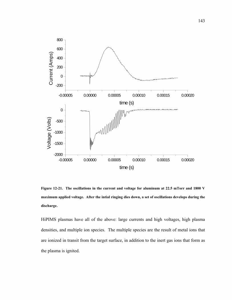
143
-0.00005 0.00000 0.00005 0.00010 0.00015 0.00020-2000
-1500
-1000
-500
0
Volta
ge (V
olts
)
time (s)
-0.00005 0.00000 0.00005 0.00010 0.00015 0.00020
-200
0
200
400
600
800
Cur
rent
(Am
ps)
time (s)
Figure 12-21. The oscillations in the current and voltage for aluminum at 22.5 mTorr and 1800 V
maximum applied voltage. After the intial ringing dies down, a set of oscillations develops during the
discharge.
HiPIMS plasmas have all of the above: large currents and high voltages, high plasma
densities, and multiple ion species. The multiple species are the result of metal ions that
are ionized in transit from the target surface, in addition to the inert gas ions that form as
the plasma is ignited.
144
The plasma sheath oscillations are expected to be strongly damped by collisions due to
their low frequency. The plasma sheath instabilities therefore will only appear when
significant currents are applied. Collisional dampening also explains the lack of
oscillations for the heavier metals as slower oscillations are more strongly damped in
comparison to the lighter elements such as aluminum such as the chromium pulses shown
in Figure 12-4.
12.7 HiPIMS plasma analysis
The magnetron sputtering plasma is a dense plasma close to the cathode (78). The
plasma is confined through magnetic fields intersecting the surface of the cathode at two
points. These magnetic fields trap electrons close to the target/cathode and through
ambipolar diffusion maintain a quasi-neutral dense plasma near the cathode. The plasma
varies in density within the chamber, and especially near the cathode (18). The plasma
density gradient results in a pressure gradient. As discussed in chapter 5, the plasma
density plays a role in the sheath thickness and the resulting sheath currents.
In HiPIMS, the previous pulse’s plasma is dissipating as the next pulse is initiated. As
the plasma is initiated, the HiPIMS pulse, utilizing the remaining plasma, will generate an
intense current spike as the ionized gas accelerates toward the target across the expanding
sheath indicative of a matrix ion sheath. The ions that just accelerated across the sheath,
sputter the target and eject secondary electrons.
The sputtered material then traverses back across the sheath in its journey toward the
substrate. The emitted electrons are accelerated across the sheath, providing a large

145
number of electrons with high ionization capability, and traverse the sheath faster than
the sputtered material due to their charge and mass.
The sheath begins collapsing to develop a new steady state sheath dependent upon the
decreasing applied voltage while the trapped electrons begin increasing the plasma
density. Due to the large number of electrons, and the lower ionization energy for metals,
the sputtered flux is ionized maintaining the quasi-neutrality of the high density HiPIMS
plasma near the cathode.
The HiPIMS plasma now becomes primarily a metallic ion plasma. The plasma sheath
now has at least two ionic species accelerating across the sheath. The multiple species
means that there will be different velocities within the sheath (98). The plasma density
is also higher than required for steady state maintenance of the sheath due to the large
number of secondary electrons emitted from the cathode. The high plasma density and
high currents begin to match the criteria for an unstable sheath (96). When this is
combined with lighter elements such as aluminum comprising the ion species, the
collisional damping of the instability will be reduced, and the likelihood for oscillations
improves even further. The collapsing sheath of the PIII model also provides an
explanation for the shift in frequency of the aluminum oscillations shown in Figure 12-15
and Figure 12-21. The time to traverse the sheath may be expected to become reduced as
the sheath shrinks to its steady state thickness. The sheath will also collapse due to the
increased pressure developed through the increased plasma density as in equation (5-17)
discussed again in Chapter 8 section 8.1 and repeated here:

146
(12-10)
After the sheath begins to collapse, self-sputtering begins to occur with the metallic ion
species (100).
As the metallic ions are used for sputtering, and the voltage begins to decrease, the
current in the cathode also drops. The HiPIMS current pulse ends in a small flow of
current that maintains the cathode voltage in the range of 0 to 500V until the pulse is
completed. At this point, there is a decaying residual plasma in the chamber with which
to initiate the next HiPIMS pulse.
The PIII model and plasma ion sheath instabilities fit well into the experimental data for
HiPIMS processes. The two concepts also help with the related process patented by
Chistyakov. A figure from the patent of Chistyakov describing the I-V characteristics is
shown in Figure 12-22 (20). The patent describes applying the voltage to a cathode in a
way to develop more power than would be expected. The power is generated by making
a step increase in the voltage, which in turn steps up the current. The voltage that
generates the large current is seen to have a small oscillation associated with the larger
current. The exact amplitude of this oscillation is not necessarily known, as the data
acquired are close to the Nyquist rate. This may be seen by the drawn in peaks earlier in
the pulse.

147
Figure 12-22. Current and voltage are graphed with respect to time from Chistyakov's patent Figure
5C. The figure shows a dramatic increase in current being generated by a quick change in the
applied voltage. As may be seen by the drawn in peaks, the frequencies are close to the Nyquist rate
of the measurement.
The PIII model in conjunction with an instability in the sheath, fits the effect of the
increased current seen by Chistyakov. The oscillating sheath exposes a large number of
ions to the accelerating voltage of the sheath at one time, and the sheath instability may
be pumped by the oscillation in the power supply. Thus the modified PIII behavior
appears to be a good fit for HiPIMS and related processes.

148
12.8 Sheath and PIII Implications
There are several implications of applying the plasma sheath instability and PIII behavior
to the HiPIMS field. For instance, during reactive sputtering with nitrogen, or at the
beginning of a run after venting, the target voltage will likely oscillate (even for higher
mass targets) as the targets have the surface oxides and nitrides removed. These
oscillations would be due to multiple ion species in the plasma sheath. This in turn
provides the operator with a method to determine the cleanliness of the target.
Another implication of the matrix sheath is in the timing and length of the pulse. Shorter
pulses should provide better sputter yields as they consume the local argon plasma
without switching to a metallic sputtering process. Another key implication is in the
necessity for a high initial plasma density.
The lower resistivity curve for the higher strength magnetic fields discussed earlier this
chapter also connects back to the sheath behavior. The sheath increases in current
density through increased plasma density, and a smaller sheath thickness which directly
affects the current flow per equation (12-10).
The fields of PIII and sheath instability research have a wealth of information for
understanding the HiPIMS plasma well beyond the oscillations (101). Within the PIII
field of study, there are predictions for the expected ion energy distributions, which will
further help characterize the HiPIMS process, and the exact nature of this moving
magnetized sheath. Overall this dissertation has found a key piece to the HiPIMS plasma
puzzle in the work of Plasma Immersion Ion Implantation (PIII) and sheath instabilities.

149
Chapter 13 Summary and future work
13.1 Summary
The goal of this dissertation was to explore causes of the oscillations found in the current
and voltage vs. time curves for HiPIMS processes. This dissertation found that a
combination of sheath instabilities and a moving matrix sheath similar to the behavior of
plasma immersion ion implantation help explain the behaviors observed experimentally.
This goal was achieved through a combination of analyzing the underlying mathematical
relationships, developing computer simulations, comparing the results to the
experimental data, and analyzing the data with respect to known behaviors in plasma
physics.
The underlying plasma physics was developed in the early chapters by establishing: the
sheath behavior, the effects of electric and magnetic fields; and the frequencies expected
in magnetized and nonmagnetized plasmas. In later chapters, this information was used
to: understand the work of Goree and Sheridan; infer a magnetized plasma model; and
establish a basis for the plasma immersion ion implantation field of study, and sheath
instabilities. This leads to the conclusion that the HiPIMS plasma has a behavior similar
to plasma immersion ion implantation, in particular a moving matrix sheath.
Rossnagel and Kaufmann were able to experimentally relate the thickness of the sheath
through the Child law sheath to the overall plasma impedance for a magnetron. The
sheath thickness decreases with increasing voltage satisfying both the child law sheath

150
equation, and the magnetron power law. The experimental data of this dissertation was
fit to a modified power law equation (12-2) throughout the voltage regime explored
(800V -1800 V). In the past others used two independent fit results of an n=6 regime and
an n=1 regime. A modification to explain results across the entire spectrum of this basic
magnetron power law equation of (2-2), is the addition of a basic resistive term. This n=1
term shows little dependence on the pressure, but is largely dependent on magnetic field
as the current of the magnetron increases. The currents in HiPIMS plasmas become
relatively large, and become a topic of discussion as their current flow exceeds that
predicted by Bohm diffusion (79). The excessive current flow has been outlined by
others and was discussed in the introductory chapters. Analysis of Bohm diffusion lead
to an investigation of how the current is carried in the discharge, and how oscillations
could contribute to this current.
In order to explore the role the oscillations can play in directly contributing to the current
of the system, a conceptual circuit design for a magnetron was included. The conceptual
circuit design for the plasma included a chopper circuit to account for the non-uniform,
time varying plasma and serve as a source for the oscillations. This model demonstrated
how oscillations can improve current flow within the magnetron by taking advantage of
cross field transport in a wave. The model failed however, to include the observed
voltage oscillations present on the cathode. One method for improving electron transport
from the sheath region would be to provide an oscillating frequency to the plasma for
example from an rf bias applied to the substrate or another region within the plasma. The
oscillations induced by the chopper circuit is a local variation and did not generate

151
oscillations in the modeled current and voltage curves, a more global effect is needed to
explain oscillations observed on the target current and target voltage curves. One region
that can globally affect the potential at the target is the sheath. The fluctuations at the
focus of this dissertation are in the cathode’s voltage and current, indicating a time
varying fluctuation averaged across the cathode surface.
The experimentally observed target oscillations have been analyzed by frequency,
amplitude and the derivative of the curves vs. time. Some of the target oscillations do not
dampen over time, but rather they appear to increase in amplitude. In particular for the
aluminum, the oscillations increase in frequency and amplitude. The increase is
indicative of a negative resistance or positive imaginary component in the relationship
between wave propagation and angular frequency. These oscillations appear similar to
sheath instabilities observed in other fields of plasma research (95).
The initially large spike in current occurring at the beginning of the HiPIMS pulse is
predicted by looking at sheath dynamics described in plasma immersion ion implantation
(PIII). PIII experiments and analysis by others have developed the concept of a dynamic
sheath which transitions from a matrix sheath to a Child law sheath (90). The expected
behavior of the sheath and its oscillations compares well to that of the initial current peak
within the HiPIMS system discussed within this dissertation.

152
13.2 Future work
There are some promising areas for future work that develop from this dissertation for
example, linear cathode arc reduction through active variation of an electric field and
improvement of HiPIMS currents by increasing the residual plasma.
Linear cathodes do not have the same density gradient with the oscillations of the
electrons in the linear portion of the linear cathode as described in Section 8.2.2. Linear
cathodes therefore could be improved in arc suppression by applying an alternating
current (ac) bias to the substrate or nearby ground to artificially generate plasma density
oscillations. A superimposed ac bias could potentially improve the high frequency
conductivity of the plasma, which electrons could take advantage of, in order to maintain
the positive space charge column associated with magnetron sputtering.
Second, alternative HiPIMS supply designs could be explored. In light of the plasma
immersion similarities, HiPIMS power supplies should maintain a small negative voltage
on the cathode. The small negative voltage would provide the cathode with a larger
initial plasma density with which to generate the initial burst of sputtering ions.
Third, the magnetron’s transition from the n=6 term to a resistive n=1 term should be
revisited. The resistive term makes physical sense as wires and connections should
contribute some base resistance to the overall system. However, the experimentally
determined resistance is higher than expected. The resistive term’s dependence on
magnetic field also calls into question the base resistance concept. A better candidate for
the origin of the n=1 term is the force balance between the plasma density and the applied

153
electric field that develop the sheath thickness. The sheath cannot shrink forever; it must
hit a limit; or transition to a different plasma behavior. The plasma density will also
begin to lose confinement as the pressure gradient begins to win out over the magnetic
trap, and therefore would be affected by a change in the magnet array. This force balance
likely forces the sheath to approach an asymptotic minimum sheath thickness. A sheath
limited current voltage curve should approach a limit of n=1.5 rather than n=1. As
previously described in the child law sheath current density equation, the sheath current is
dependent on voltage to the three halves power. The primary challenge in exploring this
concept is the shear number of variables in the model makes it easier to achieve a fit
regardless of their individual physical meaning.

154
13.3 Conclusion
This dissertation has identified the source of the current and voltage fluctuations found on
HiPIMS sputtering systems as a combination of a moving matrix sheath and sheath
instabilities. This identification is the first step in improving the HiPIMS process. Given
this knowledge, we now have a better understanding of the Chistyakov power supply
behavior (20), and given the knowledge of the transition from argon atoms to metal ions,
we can recognize that oscillation frequencies found in the current and voltage curves will
be dependent upon the process material sputtered, and other gases present. We can also
begin to predict how this process should behave in other processes such as reactive
sputtering. Oxygen and especially nitrogen should be expected to generate instability in
the sheath, and could even possibly be used as a measure of target, and system
cleanliness in a multilayer process. Through the better understanding of the nature of the
HiPIMS process developed within this dissertation, the building blocks to improving the
HiPIMS process have been laid.

155
References
1. B. Goranchev, V. Orlinov, and V. Popova. D.C. cathode sputtering: influence of the
oxygen content in the gas flow on the discharge current. Thin Solid Films. 1976, Vol. 33,
pp. 173-183.
2. J. A. Thornton. Influence of substrate temperature and deposition rate on structure of
thick sputtered Cu coatings. Journal of Vacuum Science and Technology. 1975, Vol. 12,
p. 830.
3. R. Messier, A. P. Giri, and R. A. Roy. Revised structure zone model for thin film
physical structure. Journal of Vacuum Science and Technology A. 1984, Vol. 2, p. 500.
4. S. R. Kirkpatrick, S. L. Rohde, D. M. Mihut, M. L. Kuruppu, J. R. Swanson III,
D. Thomson, and J. A. Woollam. Process monitoring and control of low temperature
reactively sputtered AlN . Thin Solid Films. 1998, Vol. 332, 1-2, p. 16.
5. S. M. Rossnagel, and J. Hopwood. Metal ion deposition from ionized mangetron
sputtering discharge. Journal of Vacuum Science and Technology B. 1994, Vol. 12, 1, p.
449.
6. R. K. Waits. Planar Magnetron Sputtering. [book auth.] J. L. Vossen and W. Kern.
Thin Film Processes. s.l. : Academic Press, 1978, p. 157.
7. S. Sevvana, S. Chennadi, R. K. Lakkaraju, J. Li, D. M. Mihut, and S. L. Rohde.
Rate enhancement in HIPIMS growth using secondary discharge confinement. 48th
156
Annual Technical Conference Proceedings of the Society of Vacuum Coaters. 2005, p.
720.
8. D. J. Christie, F. Tomasel, W. D. Sproul, and D. C. Carter. A novel pulsed supply
with arc handling and leading edge control as enabling technology for high power pulsed
magnetron sputtering (HPPMS). Journal of Vacuum Science and Technology A. 2004,
Vol. 22, 4, p. 1415.
9. V. Kouznetsov, K. Macák, J. M. Schneider, U. Helmersson, and I. Petrov. A novel
pulsed magnetron sputter technique utilizing very high target power densities. Surface
and Coatings Technology. 1999, Vol. 122, p. 290.
10. J. Alami, P. O. Å. Persson, D. Music, J. T. Gudmundsson, J. Bohlmark, and U.
Helmersson. Ion assisted physical vapor deposition for enhanced film properties on
nonflat surfaces. Journal of Vacuum Science and Technology A. 2005, Vol. 23, 2, p. 278.
11. U. Helmersson, M. Lattemann, J. Alami, J. Bohlmark,A.P. Ehiasarian, and J.T.
Gudmundsson. High power impulse magnetron sputtering discharges and thin films
growth: A brief review. 48th Annual Technical Conference Proceedings of the Society of
Vacuum Coaters. 2005, p. 458.
12. U. Helmersson, Z. S. Khan, and J. Alami. Ionized-PVD by pulsed sputtering of Ta
for metallization of high aspect ratio structures in VLSI. Proceedings of the 3rd
International EuroConference on Advanced SemiconductorDevices and Microsystems.
October 2000, pp. 191-195.

157
13. M. Lattemann, A. P. Ehiasarian, J. Bohlmark, P. Å. O. Persson, and U.
Helmersson. Investigation of high power impulse magnetron sputtering pretreated
interfaces for adhesion enhancement of hard coatings on steel. Surface and Coatings
Technology. 2006, Vol. 200, p. 6495.
14. D. V. Mozgrin, I. K. Fetisov, and G. V. Khodachenko. High current low-pressure
quasi-stationary discharge in a magnetic field. Plasma Physics Reports. 1995, Vol. 21, p.
400.
15. J. Musil, J. Leština, J. Vlcek, and T. Tölg. Pulsed dc magnetron discharges for
high-rate sputtering of thin films. Journal of Vacuum Science and Technology A. 2001,
Vol. 19, 2, p. 420.
16. J. Vlcek, P. Kudlacek, K. Burcalova, and J. Musil,. High-power pulsed sputtering
using a magnetron with enhanced plasma confinement. Journal of Vacuum Science and
Technology A. 2007, Vol. 25, 1, p. 42.
17. J. Bohlmark, M. Ostbye, M. Lattemann, H. Ljungcrantz, T. Rosell, and U.
Helmersson. Guiding the deposition flux in an ionized magnetron discharge. Thin Solid
Films. December 5, 2006, Vol. 515, 4, pp. 1928-1931.
18. J. W. Bradley, S. Thompson, and Y. Aranda Gonzalvo. Measurement of the
plasma potential in a magnetron discharge and the prediction of the electron drift speeds.
Plasma Sources Science and Technology. 2001, Vol. 10, p. 490.

158
19. K. Sarakinos, J. Alami, and M. Wuttig. Process characteristics and film properties
upon growth of TiOx films by high power pulse sputtering. Journal of Physics D:
Applied Physics. 2007, Vol. 40, p. 2108.
20. R. Chistyakov. Methods and apparatus for generating strongly-ionized plasmas with
ionizational instabilities. US 2005/0184669 USA, August 25, 2005.
21. G. Lin, Z. Ding, D. Qi, Y. Zhao, N. Wang, and C. Dong. Plasma load characteristic
of pulsed-bias arc ion plating. Journal of Vacuum Science and Technology A. 2003, Vol.
21, 5, p. 1675.
22. M. A. Lieberman, and A. J. Lichtenberg. Principles of Plasma Discharges and
Materials. New York : John Wiley & Sons, 1994.
23. J. A. Thornton. Magnetron sputtering: basic physics and application to cylindrical
magnetrons. Journal of Vacuum Science and Technology. 1978, Vol. 15, p. 171.
24. S. L. Rohde. Unbalanced Magnetron Sputtering. [book auth.] M. Francombe and J.
Vossen. Physics of Thin Films Advances in Research and Development Vol.18: Plasma
Sources for Thin Film Deposition and Etching. New York : Academic Press, 1994.
25. J. H. Boo, M. J. Jung, H. K. Park, K. H. Nam, and J. G. Han. High-rate
deposition of copper thin films usingnewly designed high-power magnetron sputtering
source. Surface and Coatings Technology. 2004, Vols. 188-189, p. 721.
26. A. G. Spencer, and R. P. Howson. Rf Oscillations in dc planar sputtering
magnetrons. Vacuum. 1988, Vol. 38, 6, p. 497.

159
27. E. Martines, M. Zuin, V. Antoni, R. Cavazzana, G. Serianni, M. Spolaore, and
C. Nakashima. Experimental investigation of low-frequency waves propagating in a
direct current planar magnetron plasma. Physics of Plasmas. 2004, Vol. 11, 5, p. 1938.
28. T. E. Sheridan, and J. Goree. Low frequency turbulent transport in magnetron
plasmas. Journal of Vacuum Science and Technology A. 1989, Vol. 7, 3, pp. 1014-1018.
29. T. E. Sheridan, M. J. Goeckner, and J. Goree. Electron and ion transport in
magnetron plasmas. Journal of Vacuum Science and Technology A. 1990, Vol. 8, 3, p.
1623.
30. J. Goree, and T. E. Sheridan. Magnetic field dependence of sputtering magnetron
efficiency. Applied Physics Letters. 1991, Vol. 59, 9, p. 1052.
31. T. E. Sheridan, M. J. Goeckner, and J. Goree. Model of energetic electron
transport in magnetron discharges. Journal of Vacuum Science and Technology A. 1990,
Vol. 8, 1, p. 30.
32. J. E. Miranda, M. J. Goeckner, J. Goree, and T. E. Sheridan. Monte Carlo
simulation of ionization in a magnetron plasma. Journal of Vacuum Science and
Technology A. 1990, Vol. 8, 3, p. 1627.
33. T. E. Sheridan, M. J. Goeckner, and J. Goree. Pressure dependence of ionization
efficiency in sputtering magnetrons. Applied Physics Letters. 1990, Vol. 57, 20, pp. 2080-
2082.

160
34. P. Kudrna, M. Holik, O. Bilyk, O. Marek, A. Behnke, E. Martines, and M.
Tichy. Langmuir probe study of the floating potential fluctuations in the dc cylindrical
magnetron discharge. [ed.] J. Meichsner and D. Loffhagen. Proceeding of the XXVI
International Conference on Phenomena in Ionized Gases. 2003, Vol. 4, p. 157.
35. E. Martines, R. Cavazzana, G. Serianni, M. Spolaore, L. Tramontin, M. Zuin,
and V. Antoni. Electrostatic fluctuations in a direct current magnetron sputtering plasma.
Physics of Plasmas. 2001, Vol. 8, 6, p. 3042.
36. T. A. van der Straaten, N. F. Cramer, I. S. Falconer, and B. W. James. The
cylindrical dc magnetron discharge: I. Particle-in-cell simulation. Journal of Physics D:
Applied Physics. 1998, 31, p. 177.
37. T. Hurtig, N. Brenning, and M. Raadu. The penetration of plasma clouds across
magnetic boundaries:The role of high frequency oscillations. Physics of Plasmas. 2004,
Vol. 11, 7, p. 33.
38. D. Lundin, U. Helmersson, S. Kirkpatrick, S. L. Rohde, and N. Brenning.
Anamalous electron transport in high power impulse magnetron sputtering. Plasma
Sources Science and Technology. 2008, Vol. 17, 2.
39. R. Sobbia, P. K. Browning, and J. W. Bradley. Numerical investigation via three-
dimensional Monte Carlo modeling of sputtering and deposition processes in a direct
current unbalanced magnetron discharge. Journal of Vacuum Science and Technology A.
2008, Vol. 26, 1, p. 103.

161
40. J. E. Greene. Epitaxial crysal growth by sputter deposition: Applications to
semiconductors. Part I. Critical Reviews in Solid State and Materials Science. 1983, Vol.
11, 1, pp. 47-97.
41. R. Glang, and L. I. Maissel, [ed.]. Handbook of Thin Film Technology. New York :
Mcgraw-Hill Book Company, 1970.
42. M. Ohring. The Materials Science of Thin Films. San Diego : Academic Press Inc.,
1992. pp. 104-114.
43. —. The Materials Science of Thin Films. San Diego : Academic Press Inc., 1992. pp.
203-208.
44. —. The Materials Science of Thin Films. San Diego : Academic Press Inc., 1992. pp.
147-198.
45. W. Kern, and J. L. Vossen. Thin Film Processes. San Diego : Academic Press Inc.,
1978. p. 11.
46. A. J. Lichtenberg, and M. A. Lieberman. Principles of Plasma Discharges and
Materials Processing. New York : John Wiley & Sons, Inc., 1994. pp. 451-453.
47. R. Messier, A. P. Giri, and R. A. Roy. Revised structure zone model for thin film
physical structure. Journal of Vacuum Science and Technology A. 1984, Vol. 2, p. 500.
48. M. Ohring. The Materials Science of Thin Films. San Diego : Academic Press Inc.,
1992. pp. 129-131.

162
49. W. Kern, and J. L. Vossen. Thin Film Processes. San Diego : Academic Press, Inc.,
1978. p. 157.
50. —. Thin Film Processes. San Diego : Academic Press, Inc., 1978. p. 27.
51. W.-D. Munz, S. L. Rohde, and W. D. Sproul. [ed.] D. S. Rickerby and A.
Matthews. Advanced Surface Coatings. New York : Chapman and Hall, 1991.
52. S. Berg, H. O. Blom, T. Larsson, and C. Nender. Modeling of reactive sputtering
of compound materials. Journal of Vacuum Science and Technology A. March 1987, Vol.
5, 2, pp. 202-207.
53. B. Chapman. Glow Discharge Processes. New York : John Wiley & Sons, Inc.,
1980.
54. S. L. Rohde, I. Petrov, W. D. Sproul, S. A. Barnett, P. J. Rudnik, and M. E.
Graham. Effects of an unbalanced magnetron in a unique dual-cathode, high rate
reactive sputtering system. Thin Solid Films. 1990, Vols. 193-194, pp. 117-126.
55. Clarke, P. J. Journal of Vacuum Science and Technology. Magnetron dc reactive
sputtering of titanium nitride and indium–tin oxide, 1977, Vol. 14, 1, pp. 141-142.
56. W. Kern, and J. L. Vossen. Thin Film Processes. San Diego : Academic Press, Inc,
1978. pp. 14-18.

163
57. W. D. Sproul, M. E. Graham, M. S. Wong, S. Lopez, D. Li, and R. A. Scholl.
Reactive direct current magnetron sputtering of aluminum oxide coatings. Journal of
Vacuum Science and Technolgoy A. May 1995, Vol. 13, 3, pp. 1188-1191.
58. K. Koski, J. Holsa, and P. Juliet. Voltage controlled reactive sputtering process for
aluminium oxide thin films. Thin Solid Films. August 4, 1998, Vol. 326, 1-2, pp. 189-
193.
59. B. Goranchev, V. Orlinov, V. Tsaneva, and I. Petrov. Direct current reactive
sputtering of aluminium. Thin Solid Films. August 1978, Vol. 52, 3, pp. 365-371.
60. S. R. Kirkpatrick, S. L. Rohde, D. M. Mihut, M. L. Kuruppu, J. R. Swanson III,
D. Thomson, and J. A. Woollam. Process monitoring and control of low temperature
reactively sputtered AlN. Thin Solid Films. 1998, Vol. 332, p. 16.
61. J. M. Schneider, W. D. Sproul, R. W. J. Chia, M.-S. Wong, and A. Matthews.
Very-high-rate reactive sputtering of alumina hard coatings. Surface and Coatings
Technology. November 25, 1997, Vol. 96, 2-3, pp. 262-266.
62. J. M. Schneider, W. D. Sproul, and A. Matthews. Phase formation and mechanical
properties of alumina coatings prepared at substrate temperatures less than 500°C by
ionized and conventional sputtering. Surface and Coatings Technology . October 1997,
Vols. 94-95, pp. 179-183.

164
63. J. P. Lehan, R. B. Sargent, and R. E. Klinger. High-rate aluminum oxide
deposition by MetaMode reactive sputtering. Journal of Vacuum Science and Technology
A. November 1992, Vol. 10, 6, pp. 3401-3406.
64. I. Ivanov, L. Hultman, K. Jarrendahl, P. Martensson, J.-E. Sundgren, B.
Hjorvarsson, and J. E. Greene. Growth of epitaxial AlN(0001) on Si(111) by reactive
magnetron sputter deposition. Journal of Applied Physics. November 1, 1995, Vol. 78, 9,
pp. 5721-5726.
65. W. Otano-Rivera, L. J. Pilione, J. A. Zapien, and R Messier. Cubic boron nitride
thin film deposition by unbalanced magnetron sputtering and dc pulsed substrate biasing.
Journal of Vacuum Science and Technology A. May 1998, Vol. 16, 3, pp. 1331-1335.
66. W. Kern, and J. L. Vossen. Thin Film Processes. San Diego : Academic Press, Inc.,
1978. p. 131.
67. U. Helmersson, Z. S. Khan, and J. Alami. Ionized-PVD by pulsed sputtering of Ta
for metallization of high aspect ratio structures in VLSI. Proceedings of the 3rd
International EuroConference on Advanced Semiconductor Devices and Microsystems.
October 2000, pp. 191-195.
68. S. Chennadi, D. J. Christie, S. Sevvana, R. K. Lakkaraju, J. Li, D. M. Mihut,
and S. L. Rohde. HIPIMS deposition of copper films: Correlation of experiments to
model predictions. 48th Annual Technical Conference Proceedings of the Society of
Vacuum Coaters. 2005, p. 474.

165
69. N. Saviddes, and B. Window. Diamond-like amorphous carbon film prepared by
magnetron sputtering. Journal of Vacuum Science and Technology A. November 1985,
Vol. 3, 6, pp. 2386-2390.
70. D. J. Christie, W. D. Sproul, D. C. Carter, and F. Tomasel. A novel pulsed supply
wiith arc handling and leading edge control as enabling technology for High Power
Pulsed Magnetron Sputtering (HPPMS). Society of Vacuum Coaters 47th Annual
Technical Conference Proceedings. 2004, pp. 113-118.
71. J. Bohlmark, J. Alami, C. Christou, A. P. Ehiasarian, and U. Helmersson.
Ionization of sputtered metals in high power pulsed magnetron sputtering. Journal of
Vacuum Science and Technology A . Jan/Feb 2005, Vol. 23, 1, pp. 18-22.
72. U. Helmersson, M. Lattemann, J. Bohlmark, A. P. Ehiasarian, and J. T.
Gudmundsson. Ionized physical vapor deposition (IPVD): A review of technology and
applications. Thin Solid Films. 2006, Vol. 513, pp. 1-24.
73. K. Macak, V. Kouznetsov, J. Schneider, and U. Helmersson. Ionized sputter
deposition using an extremely high plasma density pulsed magnetron discharge. Journal
of Vacuum Science and Technology A. July/August 2000, Vol. 18, 4, p. 1533.
74. J. A. Thornton, and A. S. Penfold. Cylindrical Magnetron Sputtering. [book auth.]
J. L. Vossen and W. Kern. Thin Film Processes. New York : Academic Press, 1978, p.
76.
75. F. F. Chen. Introduction to Plasma Physics. New York : Plenum Press, 1974.

166
76. D. D. Blackwell, D. N. Walker, S. J. Messer, and W. E. Amatucci. Characteristics
of the plasma impedance probe with constant bias. Physics of Plasmas. 2005, Vol. 12, 9.
77. R. T. Hilbish, R. M. Montgomery, and R. A. Holmes. Frequency conversion in the
sheath capacitance of a glow discharge plasma. Journal of Applied Physics. 1968, Vol.
39, 12, p. 5782.
78. S. M. Rossnagel, and H. R. Kaufman. Charge transport in magnetrons. Journal of
Vacuum Science and Technology A. 1987, Vol. 5, 4, p. 2276.
79. J. Bohlmark, U. Helmersson, M. VanZeeland, I. Axnas, J. Alami, and N.
Brenning. Measurement of the magnetic field change in a pulsed high current magnetron
discharge. Plasma Sources Science and Technology. 2004, Vol. 13, 4, p. 654.
80. J. D. Cobine. Gaseous Conductors: Theory and Engineering Applications. New
York : Dover, 1958.
81. S. R. Kirkpatrick, D. Lundin, U. Helmersson, and S. L. Rohde. Magnetized
magnetron plasma modeling. 50th Annual Technical Conference Proceedings. 2007, p.
135.
82. D. A. Glocker, M. M. Romach, D. J. Christie, and W. D. Sproul. High power
pulsed reactive sputtering of zirconium oxide and tantalum oxide. 47th Annual Technical
Conference Proceedings. April 2004, p. 183.
83. B. M. DeKoven, P. R. Ward, R. E. Weiss, D. J. Christie, R. A. Scholl, W. D.
Sproul, F. Tomasel, and A. Anders. Carbon thin film deposition using high power

167
pulsed magnetron sputtering. 46th Annual Technical Conference Proceedings. 2003, p.
158.
84. J. A. Thorton, and A. S. Penfold. Cylindrical Magnetron Sputtering. [book auth.]
W. Kern and J. L. Vossen. Thin Film Processes. New York : Academic Press, 1978, p.
76.
85. A. P. Ehiasarian, R. New, W.-D. Munz, L. Hultman, U. Helmersson, and V.
Kouznetsov. Influence of high power densities on the composition of pulsed magnetron
plasmas. Vacuum. 2004, Vol. 65, 2, pp. 147-154.
86. S. M. Rossnagel. Magnetron plasma diagnostic and processing implications. Journal
of Vacuum Science and Technology A. May/June 1988, Vol. 6, 3, pp. 1821-1826.
87. J. Bohlmark, M. Lattemann, J. T. Gudmundsson, A. P. Ehiasarian, Y. A.
Gonzalvo, N. Brenning, and U. Helmersson. The ion energy distributions and ion flux
composition from a high power impulse magnetron sputtering discharge. Thin Solid
Films. 2006, Vol. 515, p. 1522.
88. J. T. Gudmnundsson, J. Alami, and U. Helmersson. Spatial and temporal behavior
of the plasma parameters in a pulsed magnetron discharge. Surface and Coatings
Technology. 2002, Vol. 161, p. 249.
89. J. Bohlmark, J. T. Gudmundsson, J. Alami, M. Lattemann, and U. Helmersson.
Spatial electron density distribution in a high-power pulsed magnetron discharge. IEEE
Transactions on Plasma Science. 2005, Vol. 33, 2, p. 346.

168
90. M. A. Lieberman. Model of plasma immersion ion implantation. Journal of Applied
Physics. October 1989, Vol. 66, 7, pp. 2926-2929.
91. J. T. Scheuer, M. Shamim, and J. R. Conrad. Model of plasma source ion
implantation in planar, cylindrical, and spherical geometries. Journal of Applied Physics.
1990, Vol. 67, 3, p. 1241.
92. A. Anders. Physics of plasma-based ion implantation & deposition (PBIID) and high
power impulse magnetron sputtering (HIPIMS): A comparison. Physica status solidi. A,
Applications and materials science. 2008, Vol. 205, 4, pp. 965-970.
93. M. M. Widner, I. Alexeff, W. D. Jones, and K. E. Lonngren. Ion acoustic wave
excitation and ion sheath evolution. Physics of Fluids. 1970, Vol. 13, 10, p. 2352.
94. Yu. P. Bliokh, J. Felsteiner, and Ya. Z. Slutsker. Existence and stability of the
plasma sheath resonance near the ion plasma frequency. Europhysics Letters. 1999, Vol.
46, 6, p. 735.
95. D. Arbel, Z. Bar-Lev, J. Felsteiner, A. Rosenburg, and Ya. Z. Slutsker.
Collisionless instablility of the cathode sheath in a hollow-cathode discharge. Physical
Review Letters. November 1, 1993, Vol. 71, 18, pp. 2919-2922.
96. B. P. Pandey, and S. Roy. An explanation of the sheath instability. Physics of
Plasmas. January 2003, Vol. 10, 1.

169
97. N. Hershkowitz, E. Ko, W. Xu, and A. M. A. Hala. Presheath environment in
weakly ionized single and multipsecies plasmas. IEEE Transactions on Plasma Science.
April 2005, Vol. 33, 2, pp. 631-636.
98. R. N. Franklin. The plasma-sheath and its stability in a quiescent plasma containing
two species of positive ion. [ed.] Institute of Physics Publishing. Journal of Physics D:
Applied Physics. 2003, Vol. 36, p. 1806.
99. M. M. Widner, and T. P. Wright. Laminar interaction of counterstreaming
magnetized plasmas. Physical Review Letters. 1972, Vol. 28, 18, p. 1179.
100. Z. J. Radzimski, and W. M. Posadowski. Self sputtering with dc magnetron
source: Target material consideration. 37th Annual Technical Conference Proceedings.
1994, pp. 389-393.
101. D. Vender, G. M. W. Kroesen, and F. J. de Hoog. Signatures of the Bohm and
sheath velocities in minority-light-ion energy distributions. Physical Review E. 1995,
Vol. 51, 4, pp. 3480-3483.
102. D. J. Christie, F. Tomasel, W. D. Sproul, and D. C. Carter. Power supply with
arc handling for high peak power magnetron sputtering. Journal of Vacuum Science and
Technology A. 2004, Vol. 22, 4, p. 1415.
103. J. A. Thornton. Influence of substrate temperature and deposition rate on structure
of thick sputtered Cu coatings. Journal of Vacuum Science and Technology. 1975, Vol.
12, 4, p. 830.

170
104. V. Kouznetsov, K. Macak, J. M. Schneider, U. Helmersson, and I. Petrov. A
novel pulsed magnetron sputter technique utilizing very high target power densities.
Surface and Coatings Technology. 1999, Vol. 122, p. 290.

171
Appendix A Current and Voltage Curves vs. time for select
elemental Targets at UNL
A.1 Current and voltage vs. time curves for copper
Copper run 3mTorr, no inductor
0.000 0.005 0.010 0.015 0.020
-800
-600
-400
-200
0
200
Targ
et V
olta
ge
tim e
0.000 0.005 0.010 0.015 0.020-10
-8
-6
-4
-2
0
Targ
et C
urre
nt
V767

172
0.0000 0.0002 0.0004 0.0006 0.0008 0.0010
-800
-600
-400
-200
0
Targ
et V
olta
ge
time
0.0000 0.0002 0.0004 0.0006 0.0008 0.0010-10
-8
-6
-4
-2
0
Targ
et C
urre
nt
V827
0.0000 0.0002 0.0004 0.0006 0.0008 0.0010
-1200
-1000
-800
-600
-400
-200
0
Targ
et V
olta
ge
time
0.0000 0.0002 0.0004 0.0006 0.0008 0.0010
-22-20-18-16-14-12-10
-8-6-4-202
Targ
et C
urre
nt
1199V

173
0.000 0.005 0.010 0.015 0.020
-1000
-800
-600
-400
-200
0
Targ
et V
olta
ge
time
0.000 0.005 0.010 0.015 0.020-22-20-18-16-14-12-10
-8-6-4-202
Targ
et C
urre
nt
1015V
0.000 0.005 0.010 0.015 0.020
-1200
-1000-800-600
-400-200
0200
Targ
et V
olta
ge
time
0.000 0.005 0.010 0.015 0.020
-22-20-18-16-14-12-10
-8-6-4-202
Targ
et C
urre
nt
1151V

174
0.0000 0.0005 0.0010 0.0015 0.0020-1200
-1000
-800
-600
-400
-200
0
200
Targ
et V
olta
ge
time
0.0000 0.0005 0.0010 0.0015 0.0020
-20-18-16-14-12-10
-8-6-4-202
Targ
et C
urre
nt
1107V
0.0000 0.0005 0.0010 0.0015 0.0020-1200
-1000
-800
-600
-400
-200
0
200
Targ
et V
olta
ge
time
0.0000 0.0005 0.0010 0.0015 0.0020-20-18-16-14-12-10
-8-6-4-202
Targ
et C
urre
nt
1283

175
0.0001 0.0002 0.0003 0.0004 0.0005-1200
-1000
-800
-600
-400
-200
0
time
1.0x10⁻⁴ 2.0x10⁻⁴ 3.0x10⁻⁴ 4.0x10⁻⁴-20
-15
-10
-5
0
Targ
et C
urre
nt
1283V
0.00000 0.00002 0.00004 0.00006 0.00008 0.00010-1400
-1200
-1000
-800
-600
-400
-200
0
Targ
et V
olta
ge
time
0.00000 0.00002 0.00004 0.00006 0.00008 0.00010-14-12-10
-8-6-4-202
Targ
et C
urre
nt
1303V

176
0.0000 0.0002 0.0004 0.0006 0.0008 0.0010-1400-1200-1000
-800-600-400-200
0200
Targ
et V
olta
ge
time
0.0000 0.0002 0.0004 0.0006 0.0008 0.0010-100
-80
-60
-40
-20
0
20
Targ
et C
urre
nt
0.00015 0.00020 0.00025 0.00030 0.00035-1400-1200-1000
-800-600-400-200
0200
time
0.00015 0.00020 0.00025 0.00030 0.00035-100
-80
-60
-40
-20
0
20
Targ
et C
urre
nt
1350 V Arcing data
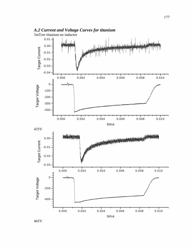
177
A.2 Current and Voltage Curves for titanium 3mTorr titanium no inductor
0.000 0.002 0.004 0.006 0.008 0.010
-400
-300
-200
-100
0
Targ
et V
olta
ge
time
0.000 0.002 0.004 0.006 0.008 0.010
-0.04
-0.03
-0.02
-0.01
0.00
0.01Ta
rget
Cur
rent
435V
0.000 0.002 0.004 0.006 0.008 0.010
-400
-200
0
Targ
et V
olta
ge
tim e
0.000 0.002 0.004 0.006 0.008 0.010
-0.03
-0.02
-0.01
0.00
Targ
et C
urre
nt
465V
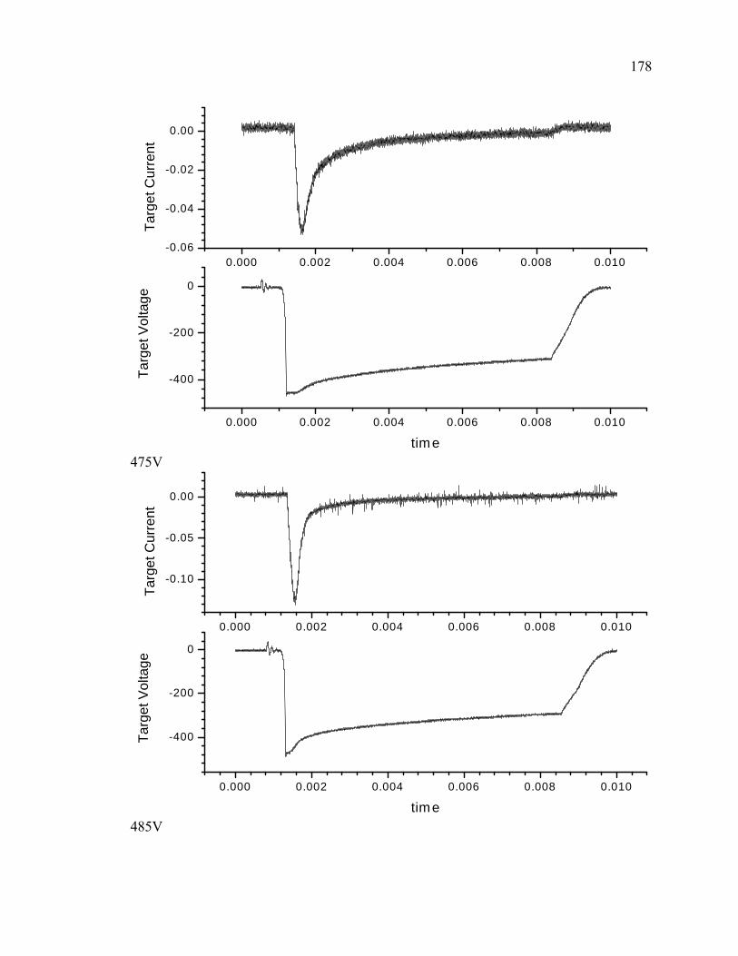
178
0.000 0.002 0.004 0.006 0.008 0.010
-400
-200
0
Targ
et V
olta
ge
time
0.000 0.002 0.004 0.006 0.008 0.010-0.06
-0.04
-0.02
0.00
Targ
et C
urre
nt
475V
0.000 0.002 0.004 0.006 0.008 0.010
-400
-200
0
Targ
et V
olta
ge
time
0.000 0.002 0.004 0.006 0.008 0.010
-0.10
-0.05
0.00
Targ
et C
urre
nt
485V

179
0.000 0.002 0.004 0.006 0.008 0.010-600
-400
-200
0
Targ
et V
olta
ge
time
0.000 0.002 0.004 0.006 0.008 0.010
-0.3
-0.2
-0.1
0.0
Targ
et C
urre
nt
538V
0.000 0.002 0.004 0.006 0.008 0.010-600
-400
-200
0
Targ
et V
olta
ge
time
0.000 0.002 0.004 0.006 0.008 0.010
-0.20
-0.15
-0.10
-0.05
0.00
Targ
et C
urre
nt
542V

180
0.0000 0.0002 0.0004 0.0006 0.0008 0.0010-600
-400
-200
0
Targ
et V
olta
ge
time
0.0000 0.0002 0.0004 0.0006 0.0008 0.0010
-0.20
-0.15
-0.10
-0.05
0.00
Targ
et C
urre
nt
550V
0.0000 0.0002 0.0004 0.0006 0.0008 0.0010-600
-400
-200
0
Targ
et V
olta
ge
time
0.0000 0.0002 0.0004 0.0006 0.0008 0.0010-0.4
-0.3
-0.2
-0.1
0.0
Targ
et C
urre
nt
555V
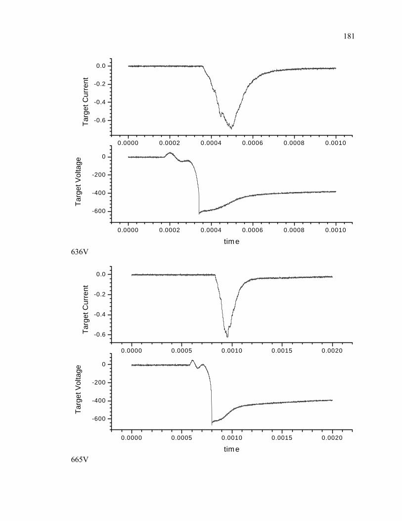
181
0.0000 0.0002 0.0004 0.0006 0.0008 0.0010
-600
-400
-200
0
Targ
et V
olta
ge
time
0.0000 0.0002 0.0004 0.0006 0.0008 0.0010
-0.6
-0.4
-0.2
0.0
Targ
et C
urre
nt
636V
0.0000 0.0005 0.0010 0.0015 0.0020
-600
-400
-200
0
Targ
et V
olta
ge
time
0.0000 0.0005 0.0010 0.0015 0.0020
-0.6
-0.4
-0.2
0.0
Targ
et C
urre
nt
665V

182
0.0000 0.0002 0.0004 0.0006 0.0008 0.0010
-800
-600
-400
-200
0
Targ
et V
olta
ge
time
0.0000 0.0002 0.0004 0.0006 0.0008 0.0010-1.2
-1.0
-0.8
-0.6
-0.4
-0.2
0.0
Targ
et C
urre
nt
810V
0.000 0.001 0.002 0.003 0.004
-1000
-800
-600
-400
-200
0
Targ
et V
olta
ge
time
0.000 0.001 0.002 0.003 0.004
-1.0
-0.8
-0.6
-0.4
-0.2
0.0
Targ
et C
urre
nt
1060V

183
0.0000 0.0002 0.0004 0.0006 0.0008 0.0010
-1200
-1000
-800
-600
-400
-200
0
Targ
et V
olta
ge
time
0.0000 0.0002 0.0004 0.0006 0.0008 0.0010
-1.0
-0.8
-0.6
-0.4
-0.2
0.0
Targ
et C
urre
nt
1135V
0.0000 0.0002 0.0004 0.0006 0.0008 0.0010
-1000
-500
0
Targ
et V
olta
ge
tim e
0.0000 0.0002 0.0004 0.0006 0.0008 0.0010
-1.0
-0.5
0.0
Targ
et C
urre
nt
1170V

184
0.000 0.001 0.002 0.003 0.004
-1200
-1000
-800
-600
-400
-200
0
Targ
et V
olta
ge
time
0.000 0.001 0.002 0.003 0.004-1.0
-0.8
-0.6
-0.4
-0.2
0.0
Targ
et C
urre
nt
1245V
0.000 0.001 0.002 0.003 0.004-1200
-1000
-800
-600
-400
-200
0
Targ
et V
olta
ge
time
0.000 0.001 0.002 0.003 0.004
-0.8
-0.6
-0.4
-0.2
Targ
et C
urre
nt
1285V

185
0.0000 0.0002 0.0004 0.0006 0.0008 0.0010
-1000
-500
0
Targ
et V
olta
ge
time
0.0000 0.0002 0.0004 0.0006 0.0008 0.0010-1.2
-1.0
-0.8
-0.6
-0.4
-0.2
0.0
Targ
et C
urre
nt
1330V 3mTorr titanium Coil at 5 Amps
0.000 0.005 0.010-700-600-500-400-300-200-100
0100
Targ
et V
olta
ge
tim e
0.000 0.002 0.004 0.006 0.008 0.010-0.35-0.30-0.25-0.20-0.15-0.10-0.050.000.05
Targ
et C
urre
nt
618V

186
0.000 0.001 0.002-700-600-500-400-300-200-100
0100
Targ
et V
olta
ge
tim e
0.0000 0.0005 0.0010 0.0015 0.0020
-0.30
-0.25-0.20-0.15
-0.10-0.05
0.000.05
Targ
et C
urre
nt
632V
0.0000 0.0002 0.0004 0.0006 0.0008 0.0010
-800-700-600-500-400-300-200-100
0
Targ
et V
olta
ge
tim e
0.0000 0.0002 0.0004 0.0006 0.0008 0.0010
-0.6
-0.4
-0.2
0.0
Targ
et C
urre
nt
788V

187
0.000 0.002 0.004 0.006 0.008 0.010-800-700-600-500-400-300-200-100
0100
Targ
et V
olta
ge
tim e
0.000 0.002 0.004 0.006 0.008 0.010
-0.6
-0.4
-0.2
0.0
Targ
et C
urre
nt
790V
0.0000 0.0005 0.0010 0.0015 0.0020-900-800-700-600-500-400-300-200-100
0100
Targ
et V
olta
ge
tim e
0.0000 0.0005 0.0010 0.0015 0.0020
-0.8
-0.6
-0.4
-0.2
0.0
Targ
et C
urre
nt
880V

188
0.00000 0.00005 0.00010 0.00015 0.00020
-1000
-500
0
Targ
et V
olta
ge
time
0.00000 0.00005 0.00010 0.00015 0.00020
-0.6
-0.4
-0.2
0.0
Targ
et C
urre
nt
1196V
0.000 0.002 0.004 0.006 0.008 0.010-1400-1200-1000
-800-600-400-200
0200
Targ
et V
olta
ge
time
0.000 0.002 0.004 0.006 0.008 0.010
-0.6
-0.4
-0.2
0.0
Targ
et C
urre
nt
1268V

189
0.0000 0.0005 0.0010 0.0015 0.0020-1400-1200-1000
-800-600-400-200
0200
Targ
et V
olta
ge
time
0.0000 0.0005 0.0010 0.0015 0.0020
-0.6
-0.4
-0.2
0.0
Targ
et C
urre
nt
1268V zoom
0.000 0.001 0.002 0.003 0.004
-1200
-1000-800-600
-400-200
0200
Targ
et V
olta
ge
time
0.000 0.001 0.002 0.003 0.004-0.45-0.40-0.35-0.30-0.25-0.20-0.15-0.10-0.05
Targ
et C
urre
nt
1272V

190
0.000 0.001 0.002 0.003 0.004
-1400-1200-1000
-800-600-400-200
0200
Targ
et V
olta
ge
time
0.000 0.001 0.002 0.003 0.004-0.35-0.30-0.25-0.20-0.15-0.10-0.050.000.05
Targ
et C
urre
nt
1412V
0.0000 0.0005 0.0010 0.0015 0.0020-1400-1200-1000
-800-600-400-200
0200
Targ
et V
olta
ge
time
0.0000 0.0005 0.0010 0.0015 0.0020
-0.6
-0.4
-0.2
0.0
Targ
et C
urre
nt
1448

191
0.00000 0.00002 0.00004 0.00006 0.00008 0.00010-1600-1400
-1200-1000
-800-600-400
-200
Targ
et V
olta
ge
time
0.00000 0.00002 0.00004 0.00006 0.00008 0.00010
-0.4
-0.2
0.0
Targ
et C
urre
nt
1464V (zoom) 3mTorr Titanium no coil current
0.000 0.005 0.010
-400
-200
0
Targ
et V
olta
ge
tim e
0.000 0.005 0.010
-0.08
-0.06
-0.04
-0.02
0.00
Targ
et C
urre
nt
436V

192
0.0000 0.0005 0.0010
-400
-200
0
Targ
et V
olta
ge
tim e
0.0000 0.0005 0.0010
-0.15
-0.10
-0.05
0.00
0.05
Targ
et C
urre
nt
482V
0.0000 0.0005 0.0010
-600
-400
-200
0
Targ
et V
olta
ge
tim e
0.0000 0.0005 0.0010
-0.6
-0.5-0.4-0.3
-0.2-0.1
0.00.1
Targ
et C
urre
nt
630V
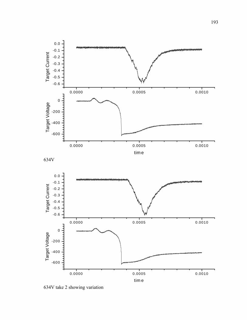
193
0.0000 0.0005 0.0010
-600
-400
-200
0
Targ
et V
olta
ge
tim e
0.0000 0.0005 0.0010
-0.6
-0.5
-0.4
-0.3
-0.2
-0.1
0.0Ta
rget
Cur
rent
634V
0.0000 0.0005 0.0010
-600
-400
-200
0
Targ
et V
olta
ge
tim e
0.0000 0.0005 0.0010
-0.6
-0.5
-0.4
-0.3
-0.2
-0.1
0.0
Targ
et C
urre
nt
634V take 2 showing variation
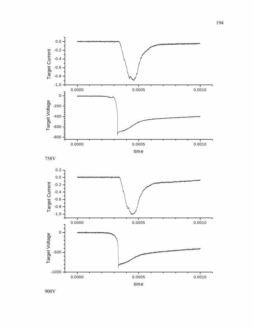
194
0.0000 0.0005 0.0010
-800
-600
-400
-200
0
Targ
et V
olta
ge
time
0.0000 0.0005 0.0010-1.0
-0.8
-0.6
-0.4
-0.2
0.0
Targ
et C
urre
nt
758V
0.0000 0.0005 0.0010-1000
-500
0
Targ
et V
olta
ge
time
0.0000 0.0005 0.0010
-1.0
-0.8
-0.6
-0.4
-0.2
0.0
0.2
Targ
et C
urre
nt
900V

195
0.000 0.005 0.010
-1000
-500
0
Targ
et V
olta
ge
time
0.000 0.005 0.010
-0.6
-0.4
-0.2
0.0
Targ
et C
urre
nt
1080V
0.000 0.005 0.010
-1000
-500
0
Targ
et V
olta
ge
time
0.000 0.005 0.010
-0.6
-0.5-0.4-0.3
-0.2-0.1
0.00.1
Targ
et C
urre
nt
1144V

196
0.0000 0.0002 0.0004
-1000
-500
0
Targ
et V
olta
ge
time
0.0000 0.0002 0.0004
-0.6
-0.4
-0.2
0.0
Targ
et C
urre
nt
1276V
0.000 0.001 0.002
-1000
-500
0
Targ
et V
olta
ge
time
0.000 0.001 0.002-0.8
-0.6
-0.4
-0.2
0.0
Targ
et C
urre
nt
1288V

197
0.000 0.005 0.010
-1500
-1000
-500
0
Targ
et V
olta
ge
time
0.000 0.005 0.010
-0.5
-0.4
-0.3
-0.2
-0.1
Targ
et C
urre
nt
1344
0.0006 0.0008 0.0010 0.0012 0.0014
-1000
-500
0
Targ
et V
olta
ge
time
0.0006 0.0008 0.0010 0.0012 0.0014
-0.5
-0.4
-0.3
-0.2
-0.1
Targ
et C
urre
nt
1344V
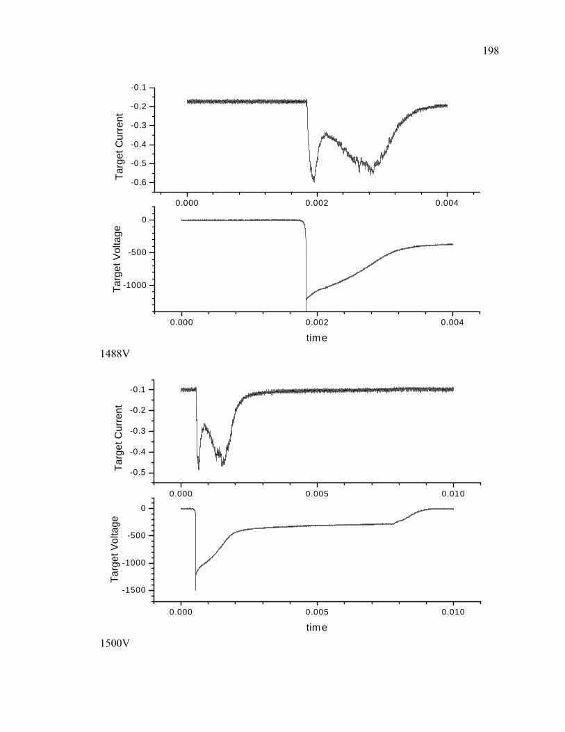
198
0.000 0.002 0.004
-1000
-500
0
Targ
et V
olta
ge
time
0.000 0.002 0.004
-0.6
-0.5
-0.4
-0.3
-0.2
-0.1
Targ
et C
urre
nt
1488V
0.000 0.005 0.010
-1500
-1000
-500
0
Targ
et V
olta
ge
time
0.000 0.005 0.010
-0.5
-0.4
-0.3
-0.2
-0.1
Targ
et C
urre
nt
1500V

199
0.000 0.002 0.004
-1000
-500
0
Targ
et V
olta
ge
time
0.000 0.002 0.004
-0.5
-0.4
-0.3
-0.2
-0.1
Targ
et C
urre
nt
1532V
0.000 0.001 0.002
-1000
-500
0
Targ
et V
olta
ge
time
0.000 0.001 0.002
-0.5
-0.4
-0.3
-0.2
-0.1
Targ
et C
urre
nt
1556V

200
A.3 Current and Voltage Curves for silver Silver 5mt coil off (silver failed to ignite at 3mtorr)
0.00 0.01 0.02 0.03 0.04
-400
-300
-200
-100
0
Targ
et V
olta
ge
time
0.00 0.01 0.02 0.03 0.04
-0.2
0.0
0.2
0.4
Targ
et C
urre
nt
360V
0.00 0.01 0.02 0.03 0.04
-400
-300
-200
-100
0
100
Targ
et V
olta
ge
tim e
0.00 0.01 0.02 0.03 0.04
-0.15
-0.10
-0.05
0.00
0.05
0.10
Targ
et C
urre
nt
400V

201
0.00 0.01 0.02 0.03 0.04-600
-400
-200
0
Targ
et V
olta
ge
time
0.00 0.01 0.02 0.03 0.04
-0.5
0.0
0.5
Targ
et C
urre
nt
515
0.00 0.01 0.02 0.03 0.04-600
-400
-200
0
Targ
et V
olta
ge
time
0.00 0.01 0.02 0.03 0.04
-0.6
-0.4
-0.2
0.0
0.2
Targ
et C
urre
nt
525

202
0.00 0.01 0.02 0.03 0.04-800
-600
-400
-200
0
Targ
et V
olta
ge
time
0.00 0.01 0.02 0.03 0.04-3
-2
-1
0Ta
rget
Cur
rent
700V
0.00 0.01 0.02
-800
-600
-400
-200
0
Targ
et V
olta
ge
time
0.00 0.01 0.02
-2
-1
0
Targ
et C
urre
nt
820

203
0.00 0.01 0.02 0.03 0.04
-800
-600
-400
-200
0
Targ
et V
olta
ge
time
0.00 0.01 0.02 0.03 0.04-4
-2
0Ta
rget
Cur
rent
870V
0.00 0.01 0.02 0.03 0.04-1000
-800
-600
-400
-200
0
Targ
et V
olta
ge
time
0.00 0.01 0.02 0.03 0.04
-3
-2
-1
0
Targ
et C
urre
nt
950V

204
0.00 0.01 0.02 0.03 0.04
-1000
-800
-600
-400
-200
0
Targ
et V
olta
ge
time
0.00 0.01 0.02 0.03 0.04
-1
0
1
Targ
et C
urre
nt
-975V
0.00 0.01 0.02 0.03 0.04-1200
-1000
-800
-600
-400
-200
0
Targ
et V
olta
ge
time
0.00 0.01 0.02 0.03 0.04
-1.0
-0.5
0.0
0.5
Targ
et C
urre
nt
1100V

205
0.00 0.01 0.02 0.03 0.04
-1000
-500
0
Targ
et V
olta
ge
time
0.00 0.01 0.02 0.03 0.04-3.0
-2.5
-2.0
-1.5
Targ
et C
urre
nt
1160V Silver 3mTorr coil on at 5 amps
0.000 0.005 0.010 0.015 0.020
-500
-400
-300
-200
-100
0
100
Targ
et V
olta
ge
T ime
0.000 0.005 0.010 0.015 0.020
-1.0
-0.5
0.0
Targ
et C
urre
nt
515V

206
0.000 0.005 0.010 0.015 0.020-600
-500
-400
-300
-200
-100
0
100
Targ
et V
olta
ge
tim e
0.000 0.005 0.010 0.015 0.020
-0.5-0.4-0.3-0.2-0.10.00.10.20.30.4
Targ
et C
urre
nt
560V
0.000 0.005 0.010 0.015 0.020
-600
-400
-200
0
Targ
et V
olta
ge
T ime
0.000 0.005 0.010 0.015 0.020-2
-1
0
1
Targ
et C
urre
nt
680V

207
0.000 0.005 0.010 0.015 0.020
-800
-600
-400
-200
0
Targ
et V
olta
ge
T ime
0.000 0.005 0.010 0.015 0.020
-1.0
-0.5
0.0
0.5
Targ
et C
urre
nt
775V
0.000 0.005 0.010 0.015 0.020
-800
-600
-400
-200
0
Targ
et V
olta
ge
T ime
0.000 0.005 0.010 0.015 0.020
-1.5
-1.0
-0.5
Targ
et C
urre
nt
800V

208
-0.005 0.000 0.005 0.010 0.015 0.020 0.025 0.030 0.035 0.040 0.045
-1000
-800
-600
-400
-200
0
Targ
et V
olta
ge
Time
-0.005 0.000 0.005 0.010 0.015 0.020 0.025 0.030 0.035 0.040 0.045
-1.5
-1.0
-0.5
Targ
et C
urre
nt
985V

209
Appendix B Current and Voltage characteristic curves for
Aluminum and Chromium at a range of pressures from LIU
system
B.1 Current and Voltage Curves for aluminum 22.5mTorr
0.00000 0.00008 0.00016
-600
-400
-200
0
Vol
tage
(Vol
ts)
time (s)
0.00000 0.00008 0.00016
0
20
40
60
Cur
rent
(Am
ps)
614 V

210
-0.00005 0.00000 0.00005 0.00010 0.00015 0.00020
-700
-600
-500-400
-300
-200-100
0
Vol
tage
(Vol
ts)
time (s)
-0.00005 0.00000 0.00005 0.00010 0.00015 0.00020-10
010203040506070
Cur
rent
(Am
ps)
670 V
-0.00005 0.00000 0.00005 0.00010 0.00015 0.00020-800-700-600-500-400-300-200-100
0
Volta
ge (V
olts
)
time (s)
-0.00005 0.00000 0.00005 0.00010 0.00015 0.00020
-100
102030405060708090
Cur
rent
(Am
ps)
718V

211
-0.00005 0.00000 0.00005 0.00010 0.00015 0.00020-900-800-700-600-500-400-300-200-100
0
Volta
ge (V
olts
)
time (s)
-0.00005 0.00000 0.00005 0.00010 0.00015 0.00020-20
020
40
6080
100
120
Cur
rent
(Am
ps)
822V
-0.00005 0.00000 0.00005 0.00010 0.00015 0.00020
-800
-600
-400
-200
0
Vol
tage
(Vol
ts)
tim e (s)
-0.00005 0.00000 0.00005 0.00010 0.00015 0.00020-40-20
020406080
100120140160
Cur
rent
(Am
ps)
832V
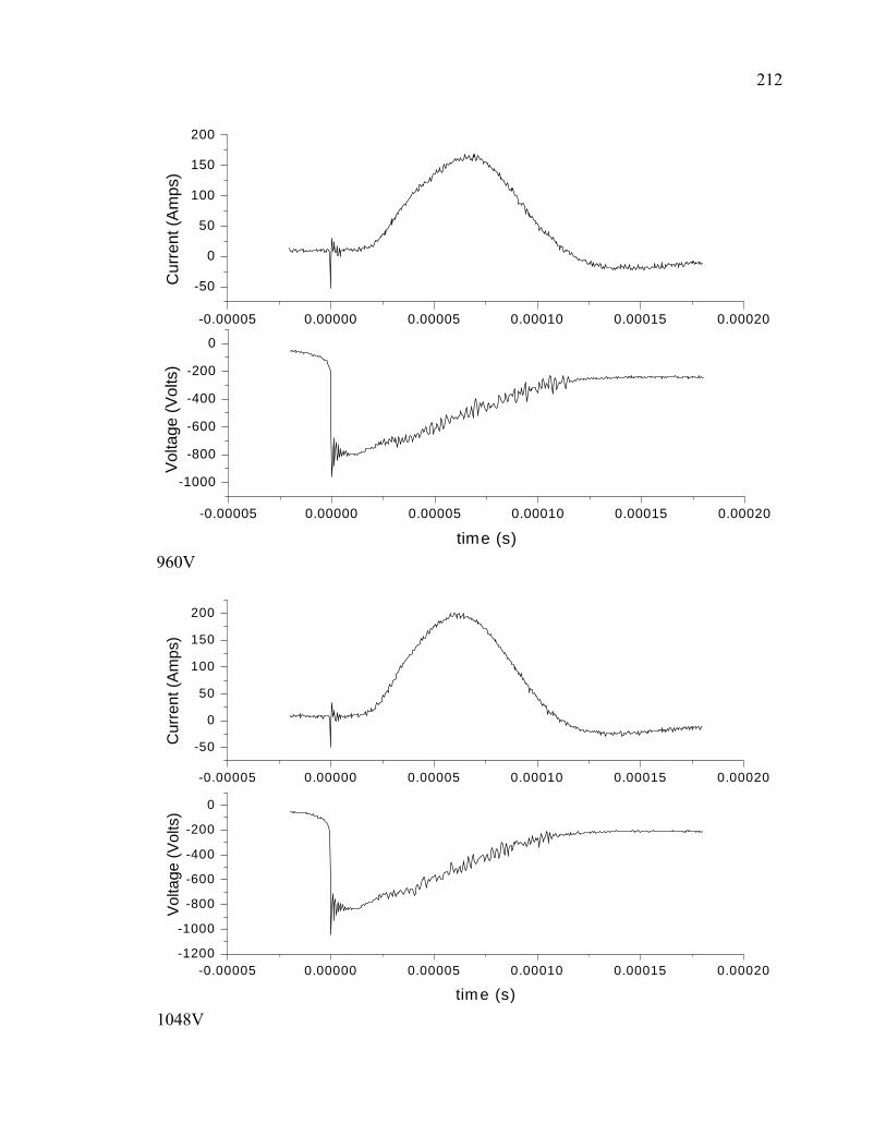
212
-0.00005 0.00000 0.00005 0.00010 0.00015 0.00020
-1000
-800
-600
-400
-200
0
Vol
tage
(Vol
ts)
time (s)
-0.00005 0.00000 0.00005 0.00010 0.00015 0.00020
-50
0
50
100
150
200
Cur
rent
(Am
ps)
960V
-0.00005 0.00000 0.00005 0.00010 0.00015 0.00020-1200
-1000
-800
-600
-400
-200
0
Vol
tage
(Vol
ts)
time (s)
-0.00005 0.00000 0.00005 0.00010 0.00015 0.00020
-50
0
50
100
150
200
Cur
rent
(Am
ps)
1048V

213
-0.00005 0.00000 0.00005 0.00010 0.00015 0.00020-1200
-1000
-800
-600
-400
-200
0
Vol
tage
(Vol
ts)
time (s)
-0.00005 0.00000 0.00005 0.00010 0.00015 0.00020
-100-50
050
100150200
250
Cur
rent
(Am
ps)
1056V
-0.00005 0.00000 0.00005 0.00010 0.00015 0.00020-1200
-1000
-800
-600
-400
-200
0
Volta
ge (V
olts
)
time (s)
-0.00005 0.00000 0.00005 0.00010 0.00015 0.00020
-100-50
050
100150200250300
Cur
rent
(Am
ps)
1064V
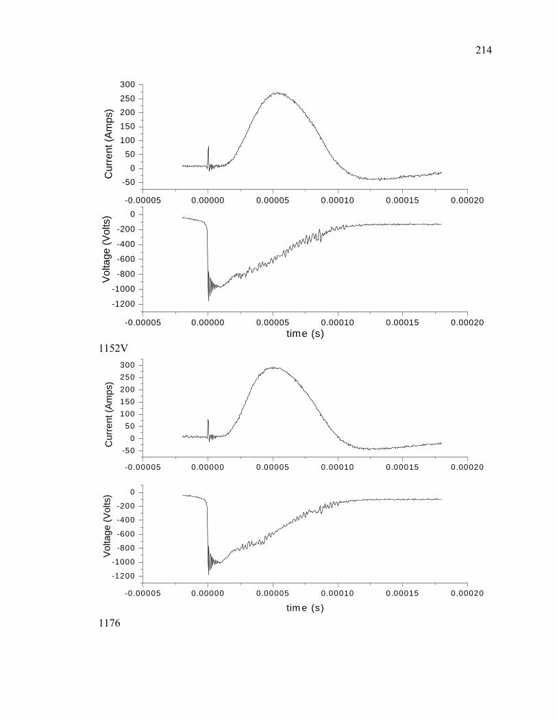
214
-0.00005 0.00000 0.00005 0.00010 0.00015 0.00020
-1200
-1000
-800
-600
-400
-200
0
Vol
tage
(Vol
ts)
time (s)
-0.00005 0.00000 0.00005 0.00010 0.00015 0.00020
-50
0
50100
150
200250
300
Cur
rent
(Am
ps)
1152V
-0.00005 0.00000 0.00005 0.00010 0.00015 0.00020
-1200
-1000
-800
-600
-400
-200
0
Vol
tage
(Vol
ts)
tim e (s)
-0.00005 0.00000 0.00005 0.00010 0.00015 0.00020
-500
50100150200250300
Cur
rent
(Am
ps)
1176

215
-0.00005 0.00000 0.00005 0.00010 0.00015 0.00020
-1400-1200-1000
-800-600-400-200
0
Volta
ge (V
olts
)
time (s)
-0.00005 0.00000 0.00005 0.00010 0.00015 0.00020-100
-500
50100150200250300350
Cur
rent
(Am
ps)
1300V
-0.00005 0.00000 0.00005 0.00010 0.00015 0.00020
-1400-1200-1000
-800-600-400-200
0
Vol
tage
(Vol
ts)
time (s)
-0.00005 0.00000 0.00005 0.00010 0.00015 0.00020-200
-100
0
100
200
300
400
Cur
rent
(Am
ps)
1400V

216
-0.00005 0.00000 0.00005 0.00010 0.00015 0.00020
-1600-1400-1200-1000
-800-600-400-200
0200
Vol
tage
(Vol
ts)
time (s)
-0.00005 0.00000 0.00005 0.00010 0.00015 0.00020-100
0
100
200
300
400
Cur
rent
(Am
ps)
1540V
-0.00005 0.00000 0.00005 0.00010 0.00015 0.00020-1600-1400-1200-1000
-800-600-400-200
0200
Vol
tage
(Vol
ts)
time (s)
-0.00005 0.00000 0.00005 0.00010 0.00015 0.00020
-200
-100
0
100
200
300
400
Cur
rent
(Am
ps)
1460V
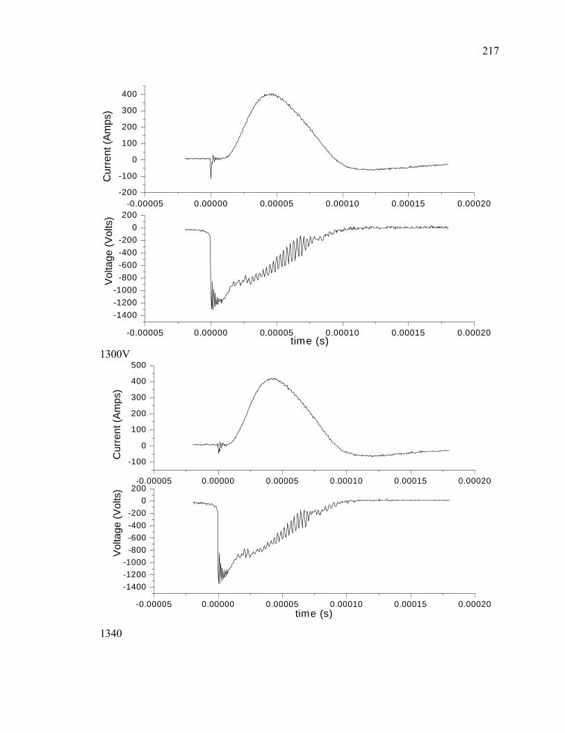
217
-0.00005 0.00000 0.00005 0.00010 0.00015 0.00020
-1400-1200-1000
-800-600-400-200
0200
Volta
ge (V
olts
)
time (s)
-0.00005 0.00000 0.00005 0.00010 0.00015 0.00020-200
-100
0
100
200
300
400C
urre
nt (A
mps
)
1300V
-0.00005 0.00000 0.00005 0.00010 0.00015 0.00020
-1400-1200-1000
-800-600-400-200
0200
Volta
ge (V
olts
)
time (s)
-0.00005 0.00000 0.00005 0.00010 0.00015 0.00020
-100
0
100
200
300
400
500
Cur
rent
(Am
ps)
1340

218
-0.00005 0.00000 0.00005 0.00010 0.00015 0.00020-1600-1400-1200-1000
-800-600-400-200
0200
Vol
tage
(Vol
ts)
time (s)
-0.00005 0.00000 0.00005 0.00010 0.00015 0.00020
-100
0
100
200
300
400
500
Cur
rent
(Am
ps)
1420V
-0.00005 0.00000 0.00005 0.00010 0.00015 0.00020-1600-1400-1200-1000
-800-600-400-200
0200
Vol
tage
(Vol
ts)
time (s)
-0.00005 0.00000 0.00005 0.00010 0.00015 0.00020
-100
0
100
200
300
400
500
Cur
rent
(Am
ps)
1440V

219
-0.00005 0.00000 0.00005 0.00010 0.00015 0.00020-1600-1400-1200-1000
-800-600-400-200
0200
Vol
tage
(Vol
ts)
time (s)
-0.00005 0.00000 0.00005 0.00010 0.00015 0.00020-300-200-100
0100200300400500
Cur
rent
(Am
ps)
1440V
-0.00005 0.00000 0.00005 0.00010 0.00015 0.00020-2000
-1500
-1000
-500
0
Volta
ge (V
olts
)
time (s)
-0.00005 0.00000 0.00005 0.00010 0.00015 0.00020-300-200-100
0100200300400500600
Cur
rent
(Am
ps)
1820V

220
-0.00005 0.00000 0.00005 0.00010 0.00015 0.00020
-1600-1400-1200-1000
-800-600-400-200
0200
Volta
ge (V
olts
)
time (s)
-0.00005 0.00000 0.00005 0.00010 0.00015 0.00020
-100
0
100200
300
400500
600
Cur
rent
(Am
ps)
1520V
-0.00005 0.00000 0.00005 0.00010 0.00015 0.00020
-1600-1400-1200-1000
-800-600-400-200
0200
Volta
ge (V
olts
)
time (s)
-0.00005 0.00000 0.00005 0.00010 0.00015 0.00020
-200-100
0100200300400500600
Cur
rent
(Am
ps)
1560V

221
-0.00005 0.00000 0.00005 0.00010 0.00015 0.00020-2000
-1500
-1000
-500
0
Vol
tage
(Vol
ts)
time (s)
-0.00005 0.00000 0.00005 0.00010 0.00015 0.00020
-1000
100200300400500600
Cur
rent
(Am
ps)
1620V
-0.00005 0.00000 0.00005 0.00010 0.00015 0.00020-2000
-1500
-1000
-500
0
Vol
tage
(Vol
ts)
time (s)
-0.00005 0.00000 0.00005 0.00010 0.00015 0.00020
-200
0
200
400
600
Cur
rent
(Am
ps)
1720V

222
-0.00005 0.00000 0.00005 0.00010 0.00015 0.00020-1800-1600-1400-1200-1000
-800-600-400-200
0200
Vol
tage
(Vol
ts)
time (s)
-0.00005 0.00000 0.00005 0.00010 0.00015 0.00020
-200
0
200
400
600
Cur
rent
(Am
ps)
1660V
-0.00005 0.00000 0.00005 0.00010 0.00015 0.00020
-1800-1600-1400-1200-1000
-800-600-400-200
0200
Vol
tage
(Vol
ts)
time (s)
-0.00005 0.00000 0.00005 0.00010 0.00015 0.00020
-1000
100200300400500600700
Cur
rent
(Am
ps)
1700V

223
-0.00005 0.00000 0.00005 0.00010 0.00015 0.00020-2000
-1500
-1000
-500
0
Volta
ge (V
olts
)
time (s)
-0.00005 0.00000 0.00005 0.00010 0.00015 0.00020
-200
0
200
400
600
800
Cur
rent
(Am
ps)
1800V
-0.00005 0.00000 0.00005 0.00010 0.00015 0.00020-2000-1800-1600-1400-1200-1000
-800-600-400-200
0200
Volta
ge (V
olts
)
time (s)
-0.00005 0.00000 0.00005 0.00010 0.00015 0.00020
-1000
100200300400500600700
Cur
rent
(Am
ps)
1760V

224
15mtorr
0.00000 0.00008 0.00016-800-700-600-500-400-300-200-100
00.00000 0.00008 0.00016
0
20
40
60V
olta
ge (V
olts
)
time (s)
Cur
rent
(Am
ps)
574V
0.00000 0.00008 0.00016-700
-600
-500
-400
-300
-200
-100
0
Vol
tage
(Vol
ts)
time (s)
0.00000 0.00008 0.00016
0
20
40
60
80
Cur
rent
(Am
ps)
650V

225
0.00000 0.00008 0.00016-800-700-600-500-400-300-200-100
0
Vol
tage
(Vol
ts)
time (s)
0.00000 0.00008 0.00016
-20
0
20
40
60
80
Cur
rent
(Am
ps)
738V
0.00000 0.00008 0.00016-900-800-700-600-500-400-300-200-100
0
Volta
ge (V
olts
)
time (s)
0.00000 0.00008 0.00016-20
0
20
40
60
80
100
Cur
rent
(Am
ps)
822V

226
0.00000 0.00008 0.00016-1000
-800
-600
-400
-200
0
Volta
ge (V
olts
)
time (s)
0.00000 0.00008 0.00016
-40-20
020406080
100120140
Cur
rent
(Am
ps)
900V
0.00000 0.00008 0.00016-1000
-800
-600
-400
-200
0
Vol
tage
(Vol
ts)
time (s)
0.00000 0.00008 0.00016-40-20
020406080
100120140160
Cur
rent
(Am
ps)
884V

227
0.00000 0.00008 0.00016
-1200
-1000
-800
-600
-400
-200
0
Vol
tage
(Vol
ts)
time (s)
0.00000 0.00008 0.00016-50
0
50
100
150
200
Cur
rent
(Am
ps)
1148V
0.00000 0.00008 0.00016-1400
-1200-1000
-800-600
-400-200
0
Vol
tage
(Vol
ts)
time (s)
0.00000 0.00008 0.00016
-100-50
050
100150200250300
Cur
rent
(Am
ps)
1276V

228
0.00000 0.00008 0.00016
-1400-1200-1000
-800-600-400-200
0
Vol
tage
(Vol
ts)
time (s)
0.00000 0.00008 0.00016
0
100
200
300
Cur
rent
(Am
ps)
1372V
0.00000 0.00008 0.00016-1800-1600-1400-1200-1000
-800-600-400-200
0200
Volta
ge (V
olts
)
time (s)
0.00000 0.00008 0.00016
-200
-1000
100200
300400
500
Cur
rent
(Am
ps)
1660V

229
0.00000 0.00008 0.00016-2000
-1500
-1000
-500
0
Volta
ge (V
olts
)
time (s)
0.00000 0.00008 0.00016
-100
0
100
200
300
400
500
Cur
rent
(Am
ps)
1820V
0.00000 0.00008 0.00016
-2000
-1500
-1000
-500
0
Vol
tage
(Vol
ts)
time (s)
0.00000 0.00008 0.00016
-100
0
100
200
300
400
500
Cur
rent
(Am
ps)
1900V

230
0.00000 0.00008 0.00016
-2000
-1500
-1000
-500
0
Vol
tage
(Vol
ts)
time (s)
0.00000 0.00008 0.00016
-200-100
0100200300400500600
Cur
rent
(Am
ps)
2080V 10 mTorr aluminum
0.00000 0.00008 0.00016
-700
-600-500
-400-300
-200-100
0
Vol
tage
(Vol
ts)
time (s)
0.00000 0.00008 0.00016
-20
0
20
40
60
Cur
rent
(Am
ps)
680V
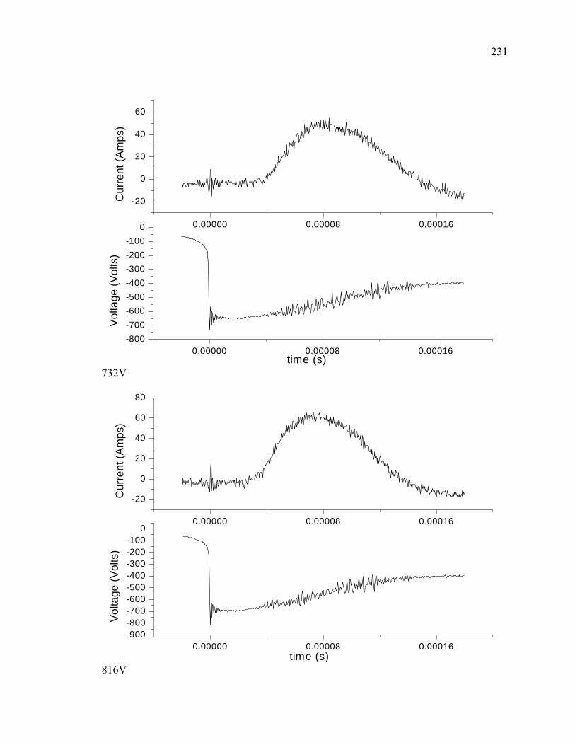
231
0.00000 0.00008 0.00016-800-700-600-500-400-300-200-100
0
Volta
ge (V
olts
)
time (s)
0.00000 0.00008 0.00016
-20
0
20
40
60C
urre
nt (A
mps
)
732V
0.00000 0.00008 0.00016-900-800-700-600-500-400-300-200-100
0
Vol
tage
(Vol
ts)
time (s)
0.00000 0.00008 0.00016
-20
0
20
40
60
80
Cur
rent
(Am
ps)
816V

232
0.00000 0.00008 0.00016-1000
-800
-600
-400
-200
0
Volta
ge (V
olts
)
time (s)
0.00000 0.00008 0.00016-40
-20
0
20
40
60
80
100
Cur
rent
(Am
ps)
876V
0.00000 0.00008 0.00016
-1000
-800
-600
-400
-200
0
Vol
tage
(Vol
ts)
time (s)
0.00000 0.00008 0.00016-40-20
020406080
100120
Cur
rent
(Am
ps)
964V

233
0.00000 0.00008 0.00016
-1200
-1000
-800
-600
-400
-200
0
Volta
ge (V
olts
)
time (s)
0.00000 0.00008 0.00016
-50
0
50
100
150
200
250
Cur
rent
(Am
ps)
1124V
0.00000 0.00008 0.00016
-1400-1200-1000
-800-600-400-200
0
Vol
tage
(Vol
ts)
time (s)
0.00000 0.00008 0.00016
-50
0
50
100
150
200
250
Cur
rent
(Am
ps)
1372V

234
0.00000 0.00008 0.00016-1600-1400-1200-1000-800-600-400-200
0
Vol
tage
(Vol
ts)
time (s)
0.00000 0.00008 0.00016-100-50
050
100150200250300350
Cur
rent
(Am
ps)
1476V
0.00000 0.00008 0.00016
-1600-1400-1200-1000
-800-600-400-200
0
Vol
tage
(Vol
ts)
time (s)
0.00000 0.00008 0.00016-100
0
100
200
300
400
Cur
rent
(Am
ps)

235
1564V
0.00000 0.00008 0.00016-1400
-1200-1000
-800-600
-400-200
0
Vol
tage
(Vol
ts)
time (s)
0.00000 0.00008 0.00016-200
-100
0
100
200
300
400
Cur
rent
(Am
ps)
1620V
0.00000 0.00008 0.00016-1800-1600-1400-1200-1000
-800-600-400-200
0200
Vol
tage
(Vol
ts)
time (s)
0.00000 0.00008 0.00016
-100
0
100
200
300
400
Cur
rent
(Am
ps)
1668V

236
0.00000 0.00008 0.00016
-1800-1600-1400-1200-1000
-800-600-400-200
0200
Volta
ge (V
olts
)
time (s)
0.00000 0.00008 0.00016
-100
0
100
200
300
400
Cur
rent
(Am
ps)
1720V
0.00000 0.00008 0.00016-2000-1800-1600-1400-1200-1000
-800-600-400-200
0200
Vol
tage
(Vol
ts)
time (s)
0.00000 0.00008 0.00016
-100
0
100
200
300
400
500
Cur
rent
(Am
ps)
1780V

237
0.00000 0.00008 0.00016
-2000
-1500
-1000
-500
0
Vol
tage
(Vol
ts)
time (s)
0.00000 0.00008 0.00016
-100
0
100
200
300
400
500
Cur
rent
(Am
ps)
1920V
0.00000 0.00008 0.00016
-2000
-1500
-1000
-500
0
Vol
tage
(Vol
ts)
time (s)
0.00000 0.00008 0.00016
-200-100
0100200300400500600
Cur
rent
(Am
ps)
2050V

238
0.00000 0.00008 0.00016-2500
-2000
-1500
-1000
-500
0
Volta
ge (V
olts
)
time (s)
0.00000 0.00008 0.00016-200-100
0100200300400500600
Cur
rent
(Am
ps)
2090V
0.00000 0.00008 0.00016-2500
-2000
-1500
-1000
-500
0
Vol
tage
(Vol
ts)
time (s)
0.00000 0.00008 0.00016-200-100
0100200300400500600
Cur
rent
(Am
ps)
2150V

239
5mTorr aluminum
-0.0001 0.0000 0.0001 0.0002 0.0003 0.0004 0.0005-10
0
10
20
30
40
Cur
rent
(Am
ps)
-0.0001 0.0000 0.0001 0.0002 0.0003 0.0004 0.0005-800-700-600-500-400-300-200-100
0
Volta
ge (V
otls
)
time (s) 732V
-0.0001 0.0000 0.0001 0.0002 0.0003 0.0004 0.0005
-10
0
10
20
30
40
50
Cur
rent
(Am
ps)
-0.0001 0.0000 0.0001 0.0002 0.0003 0.0004 0.0005
-800-700-600-500-400-300-200-100
0
Vol
tage
(Vot
ls)
time (s) 754V

240
-0.0001 0.0000 0.0001 0.0002 0.0003 0.0004 0.0005
0
100
Cur
rent
(Am
ps)
-0.0001 0.0000 0.0001 0.0002 0.0003 0.0004 0.0005
-800-700-600-500-400-300-200-100
0
Volta
ge (V
otls
)
time (s) 780V
0.0000 0.0001 0.0002-100
0
100
Cur
rent
(Am
ps)
0.0000 0.0001 0.0002
-1000
-800
-600
-400
-200
0
Vol
tage
(Vot
ls)
time (s) 988V

241
0.0000 0.0001 0.0002
0
100C
urre
nt (A
mps
)
0.0000 0.0001 0.0002
-1200
-1000
-800
-600
-400
-200
0
Volta
ge (V
otls
)
time (s) 1132V
0.0000 0.0001 0.0002
0
100
200
Cur
rent
(Am
ps)
0.0000 0.0001 0.0002
-1200
-1000
-800
-600
-400
-200
0
Vol
tage
(Vot
ls)
time (s) 1204V

242
0.0000 0.0001 0.0002-100
0
100
200
Cur
rent
(Am
ps)
0.0000 0.0001 0.0002-1400
-1200-1000
-800-600
-400-200
0
Vol
tage
(Vot
ls)
time (s) 1244V
0.0000 0.0001 0.0002
-100
0
100
200
Cur
rent
(Am
ps)
0.0000 0.0001 0.0002-1400
-1200-1000
-800-600
-400-200
0
Volta
ge (V
otls
)
time (s) 1236

243
0.0000 0.0001 0.0002-100
0
100
200C
urre
nt (A
mps
)
0.0000 0.0001 0.0002
-1200
-1000
-800
-600
-400
-200
0
Vol
tage
(Vot
ls)
time (s) 1180V
-0.00005 0.00000 0.00005 0.00010 0.00015 0.00020-100
-500
50100150200250300
Vol
tage
(Vol
ts)
-0.00005 0.00000 0.00005 0.00010 0.00015 0.00020-1600-1400-1200-1000
-800-600-400-200
0
Cur
rent
(Am
ps)
time (s) 1460

244
0.0000 0.0001 0.0002-100
0
100
200
300
Cur
rent
(Am
ps)
0.0000 0.0001 0.0002-1600-1400-1200-1000
-800-600-400-200
0
Vol
tage
(Vot
ls)
time (s) 1240
-0.00005 0.00000 0.00005 0.00010 0.00015 0.00020-200
-100
0
100
200
300
Vol
tage
(Vol
ts)
-0.00005 0.00000 0.00005 0.00010 0.00015 0.00020-1800-1600-1400-1200-1000
-800-600-400-200
0200
Cur
rent
(Am
ps)
time (s) 1620V

245
0.0000 0.0001 0.0002-200
-100
0
100
200
300
Cur
rent
(Am
ps)
0.0000 0.0001 0.0002-1400
-1200-1000
-800-600
-400-200
0
Vol
tage
(Vot
ls)
time (s)
1320V
0.0000 0.0001 0.0002-200
-100
0
100
200
300
Cur
rent
(Am
ps)
0.0000 0.0001 0.0002-1800-1600-1400-1200-1000
-800-600-400-200
0200
Vol
tage
(Vot
ls)
time (s)
1660

246
0.0000 0.0001 0.0002-200
-100
0
100
200
300
400
Cur
rent
(Am
ps)
0.0000 0.0001 0.0002
-1400-1200-1000
-800-600-400-200
0200
Vol
tage
(Vot
ls)
time (s) 1360V
0.0000 0.0001 0.0002-200
-100
0
100
200
300
400
Cur
rent
(Am
ps)
0.0000 0.0001 0.0002-1800-1600-1400-1200-1000
-800-600-400-200
0200
Vol
tage
(Vot
ls)
time (s) 1500V

247
0.0000 0.0001 0.0002-300
-200-100
0100
200300
400C
urre
nt (A
mps
)
0.0000 0.0001 0.0002-1600-1400-1200-1000
-800-600-400-200
0200
Vol
tage
(Vot
ls)
time (s) 1680
0.0000 0.0001 0.0002
-200
-1000
100200
300400
500
Cur
rent
(Am
ps)
0.0000 0.0001 0.0002
-1800-1600-1400-1200-1000
-800-600-400-200
0200
Vol
tage
(Vot
ls)
time (s) 1530V

248
0.0000 0.0001 0.0002
-100
0
100
200
300
400
500
Cur
rent
(Am
ps)
0.0000 0.0001 0.0002
-1800-1600-1400-1200-1000
-800-600-400-200
0200
Vol
tage
(Vot
ls)
time (s) 1610
0.0000 0.0001 0.0002-300-200-100
0100200300400500
Cur
rent
(Am
ps)
0.0000 0.0001 0.0002
-1600-1400-1200-1000
-800-600-400-200
0200
Vol
tage
(Vot
ls)
time (s) 1730V

249
0.0000 0.0001 0.0002-200
-1000
100200
300400
500
Cur
rent
(Am
ps)
0.0000 0.0001 0.0002-1800-1600-1400-1200-1000
-800-600-400-200
0200
Volta
ge (V
otls
)
time (s)
1610 V
0.0000 0.0001 0.0002
-200-100
0100200300400500
Cur
rent
(Am
ps)
0.0000 0.0001 0.0002
-1800-1600-1400-1200-1000
-800-600-400-200
0200
Vol
tage
(Vot
ls)
time (s) 1730V

250
0.0000 0.0001 0.0002
-100
0100
200300
400500
600
Cur
rent
(Am
ps)
0.0000 0.0001 0.0002-1800-1600-1400-1200-1000-800-600-400-200
0200
Volta
ge (V
otls
)
time (s) 1610V
0.0000 0.0001 0.0002-200-100
0100200300400500600
Cur
rent
(Am
ps)
0.0000 0.0001 0.0002-2500
-2000
-1500
-1000
-500
0
Vol
tage
(Vot
ls)
time (s) 2170V

251
B.2 Current and Voltage curves over a range of pressures for chromium 5 mtorr chromium target
-0.0001 0.0000 0.0001 0.0002 0.0003 0.0004 0.0005-700
-600-500
-400
-300-200
-100
0
Vol
tage
(Vol
ts)
time (s)
-0.0001 0.0000 0.0001 0.0002 0.0003 0.0004 0.000506
12182430364248
Cur
rent
(Am
ps)
600V
-0.0001 0.0000 0.0001 0.0002 0.0003 0.0004 0.0005
-700-600-500-400-300-200-100
0
Vol
tage
(Vol
ts)
time (s)
-0.0001 0.0000 0.0001 0.0002 0.0003 0.0004 0.0005-606
121824303642485460
Cur
rent
(Am
ps)
646V

252
-0.0001 0.0000 0.0001 0.0002 0.0003 0.0004 0.0005
-800-700-600-500-400-300-200-100
0
Vol
tage
(Vol
ts)
time (s)
-0.0001 0.0000 0.0001 0.0002 0.0003 0.0004 0.000506
12182430364248546066
Cur
rent
(Am
ps)
690V
-0.0001 0.0000 0.0001 0.0002 0.0003 0.0004 0.0005
-800-700-600-500-400-300-200-100
0
Volta
ge (V
olts
)
time (s)
-0.0001 0.0000 0.0001 0.0002 0.0003 0.0004 0.0005-40
-20
0
20
40
60
80
Cur
rent
(Am
ps)
744V
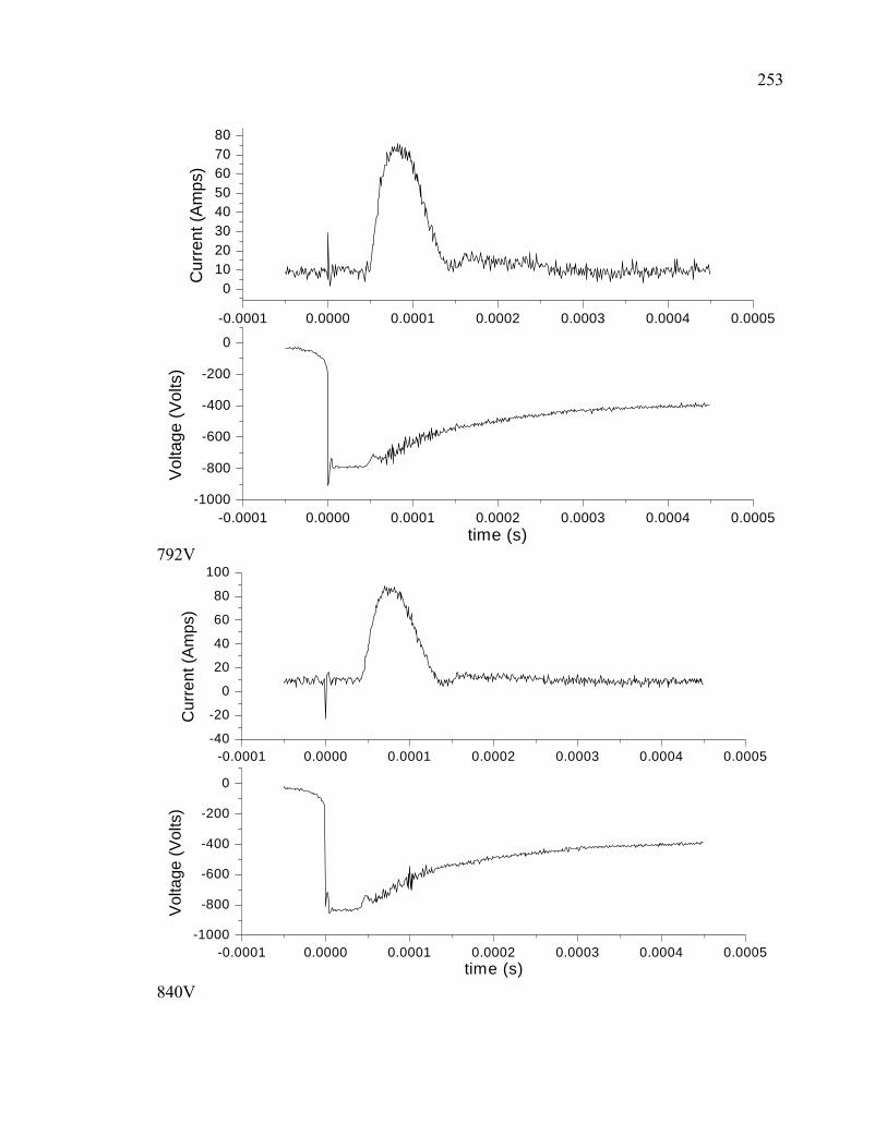
253
-0.0001 0.0000 0.0001 0.0002 0.0003 0.0004 0.0005-1000
-800
-600
-400
-200
0
Vol
tage
(Vol
ts)
time (s)
-0.0001 0.0000 0.0001 0.0002 0.0003 0.0004 0.0005
01020304050607080
Cur
rent
(Am
ps)
792V
-0.0001 0.0000 0.0001 0.0002 0.0003 0.0004 0.0005-1000
-800
-600
-400
-200
0
Vol
tage
(Vol
ts)
time (s)
-0.0001 0.0000 0.0001 0.0002 0.0003 0.0004 0.0005-40
-20
0
20
40
60
80
100
Cur
rent
(Am
ps)
840V

254
-0.00005 0.00000 0.00005 0.00010 0.00015 0.00020-1200
-1000
-800
-600
-400
-200
0
Volta
ge (V
olts
)
time (s)
-0.00005 0.00000 0.00005 0.00010 0.00015 0.00020
-200
20406080
100120
Cur
rent
(Am
ps)
880V
-0.00005 0.00000 0.00005 0.00010 0.00015 0.00020
-1200
-1000
-800
-600
-400
-200
0
Vol
tage
(Vol
ts)
time (s)
-0.00005 0.00000 0.00005 0.00010 0.00015 0.00020-40-20
020406080
100120140160
Cur
rent
(Am
ps)
936V

255
-0.00005 0.00000 0.00005 0.00010 0.00015 0.00020-1400
-1200-1000
-800
-600-400
-200
0
Vol
tage
(Vol
ts)
time (s)
-0.00005 0.00000 0.00005 0.00010 0.00015 0.00020-50
0
50
100
150
200
Cur
rent
(Am
ps)
976V
-0.00005 0.00000 0.00005 0.00010 0.00015 0.00020
-1400-1200-1000
-800-600-400-200
0
Vol
tage
(Vol
ts)
time (s)
-0.00005 0.00000 0.00005 0.00010 0.00015 0.00020
-50
0
50
100
150
200
Cur
rent
(Am
ps)
1024V

256
-0.00005 0.00000 0.00005 0.00010 0.00015 0.00020-1600-1400-1200-1000
-800-600-400-200
0
Vol
tage
(Vol
ts)
time (s)
-0.00005 0.00000 0.00005 0.00010 0.00015 0.00020
-100
-50
050
100
150200
250
Cur
rent
(Am
ps)
1072V
-0.00005 0.00000 0.00005 0.00010 0.00015 0.00020
-1600-1400-1200-1000
-800-600-400-200
0
Vol
tage
(Vol
ts)
time (s)
-0.00005 0.00000 0.00005 0.00010 0.00015 0.00020
-50
0
50
100
150
200
250
Cur
rent
(Am
ps)
1120V

257
-0.00005 0.00000 0.00005 0.00010 0.00015 0.00020-1400
-1200-1000
-800
-600-400
-200
0
Vol
tage
(Vol
ts)
time (s)
-0.00005 0.00000 0.00005 0.00010 0.00015 0.00020-150-100
-500
50100150200250300
Cur
rent
(Am
ps)
1160V
-0.00005 0.00000 0.00005 0.00010 0.00015 0.00020
-1400-1200-1000
-800-600-400-200
0
Vol
tage
(Vol
ts)
time (s)
-0.00005 0.00000 0.00005 0.00010 0.00015 0.00020-100
-500
50100150200250300
Cur
rent
(Am
ps)
1192V

258
-0.00005 0.00000 0.00005 0.00010 0.00015 0.00020
-1400-1200-1000
-800-600-400-200
0
Vol
tage
(Vol
ts)
time (s)
-0.00005 0.00000 0.00005 0.00010 0.00015 0.00020-100
-500
50100150200250300
Cur
rent
(Am
ps)
1224V
-0.00005 0.00000 0.00005 0.00010 0.00015 0.00020-1600-1400-1200-1000
-800-600-400-200
0
Vol
tage
(Vol
ts)
time (s)
-0.00005 0.00000 0.00005 0.00010 0.00015 0.00020
-100
0
100
200
300
400
Cur
rent
(Am
ps)
1280V

259
-0.00005 0.00000 0.00005 0.00010 0.00015 0.00020
-1600-1400-1200-1000
-800-600-400-200
0
Vol
tage
(Vol
ts)
time (s)
-0.00005 0.00000 0.00005 0.00010 0.00015 0.00020
-100
0
100
200
300
400
Cur
rent
(Am
ps)
1300V
-0.00005 0.00000 0.00005 0.00010 0.00015 0.00020
-1600-1400-1200-1000
-800-600-400-200
0
Volta
ge (V
olts
)
time (s)
-0.00005 0.00000 0.00005 0.00010 0.00015 0.00020
-100
0
100
200
300
400
Cur
rent
(Am
ps)
1340V

260
-0.00005 0.00000 0.00005 0.00010 0.00015 0.00020
-2000
-1500
-1000
-500
0
Vol
tage
(Vol
ts)
time (s)
-0.00005 0.00000 0.00005 0.00010 0.00015 0.00020
-100
0
100
200
300
400
Cur
rent
(Am
ps)
1380V
-0.00005 0.00000 0.00005 0.00010 0.00015 0.00020
-2000
-1500
-1000
-500
0
Volta
ge (V
olts
)
time (s)
-0.00005 0.00000 0.00005 0.00010 0.00015 0.00020
-100
0
100
200
300
400
Cur
rent
(Am
ps)
1400V

261
-0.00005 0.00000 0.00005 0.00010 0.00015 0.00020
-2000
-1500
-1000
-500
0
Vol
tage
(Vol
ts)
time (s)
-0.00005 0.00000 0.00005 0.00010 0.00015 0.00020
-100
0
100
200
300
400
Cur
rent
(Am
ps)
1440V
-0.00005 0.00000 0.00005 0.00010 0.00015 0.00020-2000
-1500
-1000
-500
0
Vol
tage
(Vol
ts)
time (s)
-0.00005 0.00000 0.00005 0.00010 0.00015 0.00020
-100
0
100
200
300
400
Cur
rent
(Am
ps)
1460V

262
-0.00005 0.00000 0.00005 0.00010 0.00015 0.00020
-1800-1600-1400-1200-1000
-800-600-400-200
0200
Volta
ge (V
olts
)
time (s)
-0.00005 0.00000 0.00005 0.00010 0.00015 0.00020
-200
-100
0100
200
300400
500
Cur
rent
(Am
ps)
1500V
-0.00005 0.00000 0.00005 0.00010 0.00015 0.00020
-1800-1600-1400-1200-1000
-800-600-400-200
0200
Vol
tage
(Vol
ts)
time (s)
-0.00005 0.00000 0.00005 0.00010 0.00015 0.00020
-200
-100
0100
200
300400
500
Cur
rent
(Am
ps)
1520V

263
-0.00005 0.00000 0.00005 0.00010 0.00015 0.00020
-2500
-2000
-1500
-1000
-500
0
Vol
tage
(Vol
ts)
time (s)
-0.00005 0.00000 0.00005 0.00010 0.00015 0.00020
-100
0
100
200
300
400
500
Cur
rent
(Am
ps)
1540V
-0.00005 0.00000 0.00005 0.00010 0.00015 0.00020-2500
-2000
-1500
-1000
-500
0
Vol
tage
(Vol
ts)
time (s)
-0.00005 0.00000 0.00005 0.00010 0.00015 0.00020
-100
0
100
200
300
400
500
Cur
rent
(Am
ps)
1580V

264
-0.00005 0.00000 0.00005 0.00010 0.00015 0.00020
-2000
-1500
-1000
-500
0
Vol
tage
(Vol
ts)
time (s)
-0.00005 0.00000 0.00005 0.00010 0.00015 0.00020
-100
0
100
200
300
400
500
Cur
rent
(Am
ps)
1600V
-0.00005 0.00000 0.00005 0.00010 0.00015 0.00020
-2000
-1500
-1000
-500
0
Vol
tage
(Vol
ts)
time (s)
-0.00005 0.00000 0.00005 0.00010 0.00015 0.00020
-200-100
0100200300400500
Cur
rent
(Am
ps)
1620V

265
-0.00005 0.00000 0.00005 0.00010 0.00015 0.00020
-2000
-1500
-1000
-500
0
Vol
tage
(Vol
ts)
time (s)
-0.00005 0.00000 0.00005 0.00010 0.00015 0.00020
-100
0
100
200
300
400
500
Cur
rent
(Am
ps)
1640V 10mTorr Chromium target
0.00000 0.00008 0.00016-700
-600-500
-400-300
-200-100
0
Vol
tage
(Vol
ts)
time (s)
0.00000 0.00008 0.00016
0
20
40
60
Cur
rent
(Am
ps)
646V

266
0.00000 0.00008 0.00016
-700-600-500-400-300-200-100
0
Vol
tage
(Vol
ts)
time (s)
0.00000 0.00008 0.00016
0
20
40
60
Cur
rent
(Am
ps)
662V
0.00000 0.00008 0.00016
-800-700-600-500-400-300-200-100
0
Vol
tage
(Vol
ts)
time (s)
0.00000 0.00008 0.00016
0
20
40
60
Cur
rent
(Am
ps)
772V
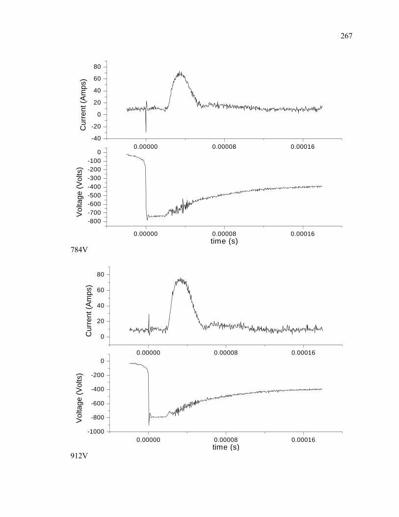
267
0.00000 0.00008 0.00016
-800-700-600-500-400-300-200-100
0
Vol
tage
(Vol
ts)
time (s)
0.00000 0.00008 0.00016-40
-20
0
20
40
60
80
Cur
rent
(Am
ps)
784V
0.00000 0.00008 0.00016-1000
-800
-600
-400
-200
0
Vol
tage
(Vol
ts)
time (s)
0.00000 0.00008 0.00016
0
20
40
60
80
Cur
rent
(Am
ps)
912V

268
0.00000 0.00008 0.00016-1000
-800
-600
-400
-200
0
Vol
tage
(Vol
ts)
time (s)
0.00000 0.00008 0.00016-40
-20
0
20
40
60
80
100
Cur
rent
(Am
ps)
880V
0.00000 0.00008 0.00016-1200
-1000
-800
-600
-400
-200
0
Vol
tage
(Vol
ts)
time (s)
0.00000 0.00008 0.00016
-200
20406080
100120
Cur
rent
(Am
ps)
1032V

269
0.00000 0.00008 0.00016
-1200
-1000
-800
-600
-400
-200
0
Vol
tage
(Vol
ts)
time (s)
0.00000 0.00008 0.00016-40-20
020406080
100120140160
Cur
rent
(Am
ps)
1176V
0.00000 0.00008 0.00016-1400
-1200-1000
-800-600
-400-200
0
Vol
tage
(Vol
ts)
time (s)
0.00000 0.00008 0.00016
-40-20
020406080
100120140160180
Cur
rent
(Am
ps)
1264V

270
0.00000 0.00008 0.00016
-1400-1200-1000
-800-600-400-200
0
Vol
tage
(Vol
ts)
time (s)
0.00000 0.00008 0.00016
-50
0
50
100
150
200
Cur
rent
(Am
ps)
1376V
0 00000 0 00008 0 00016-1600-1400-1200-1000
-800-600-400-200
0
Volta
ge (V
olts
)
0.00000 0.00008 0.00016
-100
-50
0
50
100
150
200
250
Cur
rent
(Am
ps)
1464V

271
0.00000 0.00008 0.00016
-1600-1400-1200-1000
-800-600-400-200
0
Volta
ge (V
olts
)
time (s)
0.00000 0.00008 0.00016
-50
0
50
100
150
200
250
Cur
rent
(Am
ps)
1536V
0.00000 0.00008 0.00016-1400
-1200-1000
-800-600
-400-200
0
Volta
ge (V
olts
)
time (s)
0.00000 0.00008 0.00016-150-100
-500
50100150200250300
Cur
rent
(Am
ps)
1368

272
0.00000 0.00008 0.00016-1600-1400-1200-1000
-800-600-400-200
0
Volta
ge (V
olts
)
time (s)
0.00000 0.00008 0.00016
-100
0
100
200
300
400
Cur
rent
(Am
ps)
1416V
0.00000 0.00008 0.00016
-1600-1400-1200-1000
-800-600-400-200
0
Vol
tage
(Vol
ts)
time (s)
0.00000 0.00008 0.00016
-100
0
100
200
300
400
Cur
rent
(Am
ps)
1500V

273
0.00000 0.00008 0.00016
-2000
-1500
-1000
-500
0
Vol
tage
(Vol
ts)
time (s)
0.00000 0.00008 0.00016
-100
0
100
200
300
400
Cur
rent
(Am
ps)
2040V
0.00000 0.00008 0.00016
-2000
-1500
-1000
-500
0
Vol
tage
(Vol
ts)
time (s)
0.00000 0.00008 0.00016
-100
0
100
200
300
400
Cur
rent
(Am
ps)
2080V

274
0.00000 0.00008 0.00016
-2500
-2000
-1500
-1000
-500
0
Vol
tage
(Vol
ts)
time (s)
0.00000 0.00008 0.00016
-100
0
100
200
300
400
500
Cur
rent
(Am
ps)
2340V 15mTorr Aluminum
0.00000 0.00008 0.00016-700
-600
-500
-400
-300
-200
-100
0
Vol
tage
(Vol
ts)
time (s)
0.00000 0.00008 0.00016
0
20
40
60
Cur
rent
(Am
ps)
624V
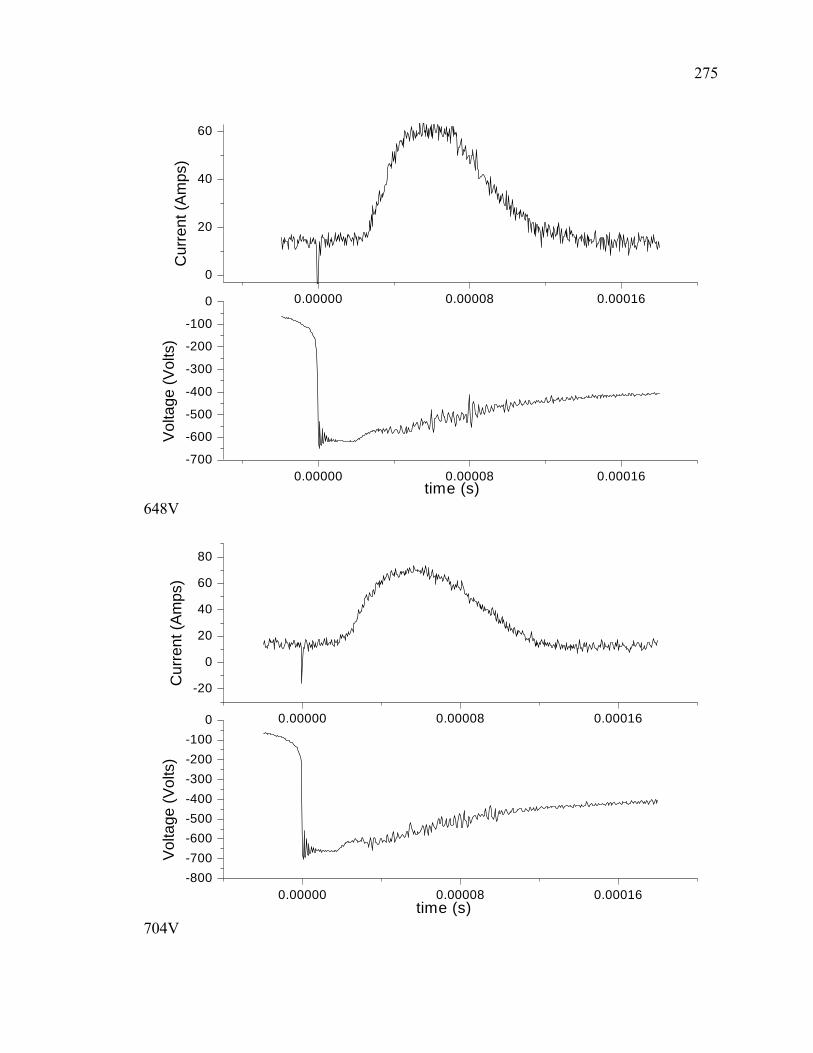
275
0.00000 0.00008 0.00016-700
-600
-500
-400
-300
-200
-100
0
Vol
tage
(Vol
ts)
time (s)
0.00000 0.00008 0.00016
0
20
40
60
Cur
rent
(Am
ps)
648V
0.00000 0.00008 0.00016-800-700-600-500-400-300-200-100
0
Volta
ge (V
olts
)
time (s)
0.00000 0.00008 0.00016
-20
0
20
40
60
80
Cur
rent
(Am
ps)
704V

276
0.00000 0.00008 0.00016
-800-700-600-500-400-300-200-100
0
Vol
tage
(Vol
ts)
time (s)
0.00000 0.00008 0.00016-20
0
20
40
60
80
100
Cur
rent
(Am
ps)
776V
0.00000 0.00008 0.00016
-800
-600
-400
-200
0
Vol
tage
(Vol
ts)
time (s)
0.00000 0.00008 0.00016
-60-40-20
020406080
100120
Cur
rent
(Am
ps)
832V

277
0.00000 0.00008 0.00016-1000
-800
-600
-400
-200
0
Vol
tage
(Vol
ts)
time (s)
0.00000 0.00008 0.00016
-80-60-40-20
020406080
100120140160
Cur
rent
(Am
ps)
920V
0.00000 0.00008 0.00016-1200
-1000
-800
-600
-400
-200
0
Vol
tage
(Vol
ts)
time (s)
0.00000 0.00008 0.00016
-200
20406080
100120140160
Cur
rent
(Am
ps)
1032V

278
0.00000 0.00008 0.00016
-1000
-800
-600
-400
-200
0
Vol
tage
(Vol
ts)
time (s)
0.00000 0.00008 0.00016-40-20
020406080
100120140160180200
Cur
rent
(Am
ps)
980V
0.00000 0.00008 0.00016-1200
-1000
-800
-600
-400
-200
0
Vol
tage
(Vol
ts)
time (s)
0.00000 0.00008 0.00016
-50
0
50
100
150
200
250
Cur
rent
(Am
ps)
1064

279
0.00000 0.00008 0.00016
-1200
-1000
-800
-600
-400
-200
0
Vol
tage
(Vol
ts)
time (s)
0.00000 0.00008 0.00016-100
-50
0
50
100
150
200
250
Cur
rent
(Am
ps)
1120V
0.00000 0.00008 0.00016-1400
-1200-1000
-800-600
-400-200
0
Vol
tage
(Vol
ts)
time (s)
0.00000 0.00008 0.00016
-50
0
50
100
150
200
250
Cur
rent
(Am
ps)
1224V

280
0.00000 0.00008 0.00016-1400
-1200-1000
-800-600
-400-200
0
Vol
tage
(Vol
ts)
time (s)
0.00000 0.00008 0.00016
-50
0
50
100
150
200
250
300
Cur
rent
(Am
ps)
1256V
0.00000 0.00008 0.00016
-1600-1400-1200-1000
-800-600-400-200
0
Vol
tage
(Vol
ts)
time (s)
0.00000 0.00008 0.00016-100
-500
50100150200250300350
Cur
rent
(Am
ps)
1520V

281
0.00000 0.00008 0.00016-1800-1600-1400-1200-1000
-800-600-400-200
0200
Vol
tage
(Vol
ts)
time (s)
0.00000 0.00008 0.00016
-300
-200-100
0100
200300
400
Cur
rent
(Am
ps)
1600V
0.00000 0.00008 0.00016
-1800-1600-1400-1200-1000
-800-600-400-200
0200
Vol
tage
(Vol
ts)
time (s)
0.00000 0.00008 0.00016-400-300-200-100
0100200300400
Cur
rent
(Am
ps)
1740V

282
0.00000 0.00008 0.00016
-2000
-1500
-1000
-500
0
Volta
ge (V
olts
)
time (s)
0.00000 0.00008 0.00016-100
0
100
200
300
400
Cur
rent
(Am
ps)
2060V
0.00000 0.00008 0.00016-2500
-2000
-1500
-1000
-500
0
Vol
tage
(Vol
ts)
time (s)
0.00000 0.00008 0.00016
-100
0
100
200
300
400
500
Cur
rent
(Am
ps)
2240V

283
0.00000 0.00008 0.00016-2500
-2000
-1500
-1000
-500
0
Vol
tage
(Vol
ts)
time (s)
0.00000 0.00008 0.00016
-100
0
100
200
300
400
500
Cur
rent
(Am
ps)
2260V 20 mTorr chromium target
0.00000 0.00008 0.00016-700
-600
-500
-400
-300
-200
-100
0
Vol
tage
(Vol
ts)
time (s)
0.00000 0.00008 0.00016-20
0
20
40
60
Cur
rent
(Am
ps)
620V

284
0.00000 0.00008 0.00016-700
-600
-500
-400
-300
-200
-100
0
Vol
tage
(Vol
ts)
time (s)
0.00000 0.00008 0.00016-20
0
20
40
60
80
Cur
rent
(Am
ps)
652V
0.00000 0.00008 0.00016-800-700-600-500-400-300-200-100
0
Vol
tage
(Vol
ts)
time (s)
0.00000 0.00008 0.00016-20
0
20
40
60
80
100
Cur
rent
(Am
ps)
704V

285
0.00000 0.00008 0.00016
-800
-600
-400
-200
0
Volta
ge (V
olts
)
time (s)
0.00000 0.00008 0.00016-40
-200
2040
6080
100
Cur
rent
(Am
ps)
832V
0.00000 0.00008 0.00016-1000
-800
-600
-400
-200
0
Vol
tage
(Vol
ts)
time (s)
0.00000 0.00008 0.00016-20
020406080
100120140
Cur
rent
(Am
ps)
904V

286
0.00000 0.00008 0.00016
-1000
-800
-600
-400
-200
0
Vol
tage
(Vol
ts)
time (s)
0.00000 0.00008 0.00016-40-20
020406080
100120140160180
Cur
rent
(Am
ps)
936
0.00000 0.00008 0.00016
-1000
-800
-600
-400
-200
0
Volta
ge (V
olts
)
time (s)
0.00000 0.00008 0.00016
-50
0
50
100
150
200
Cur
rent
(Am
ps)
960V

287
0.00000 0.00008 0.00016-1400-1200-1000
-800-600-400-200
0
Volta
ge (V
olts
)
time (s)
0.00000 0.00008 0.00016-50
0
50
100
150
200
Cur
rent
(Am
ps)
1232V
0.00000 0.00008 0.00016
-1400-1200-1000
-800-600-400-200
0
Volta
ge (V
olts
)
time (s)
0.00000 0.00008 0.00016
-50
0
50
100
150
200
250
Cur
rent
(Am
ps)
1312V

288
0.00000 0.00008 0.00016
-1400-1200-1000
-800-600-400-200
0
Volta
ge (V
olts
)
time (s)
0.00000 0.00008 0.00016
-50
0
50
100
150
200
250
Cur
rent
(Am
ps)
1340
0.00000 0.00008 0.00016
-1400-1200-1000
-800-600-400-200
0
Volta
ge (V
olts
)
time (s)
0.00000 0.00008 0.00016
0
100
200
300
Cur
rent
(Am
ps)
1373V
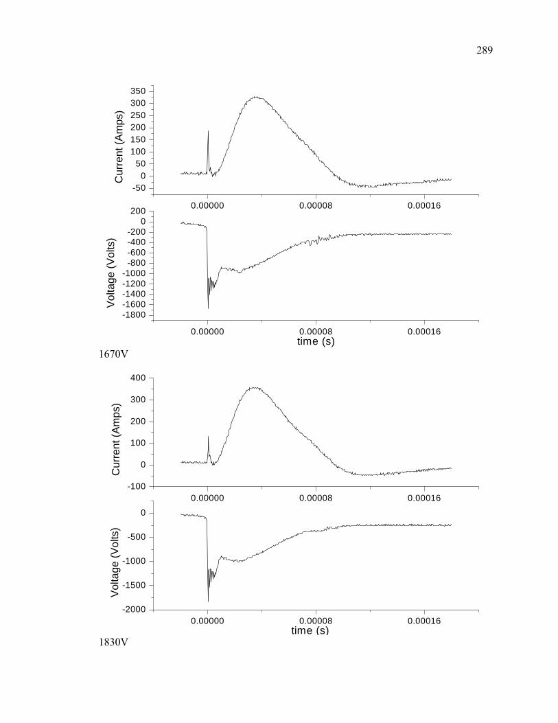
289
0.00000 0.00008 0.00016
-1800-1600-1400-1200-1000
-800-600-400-200
0200
Volta
ge (V
olts
)
time (s)
0.00000 0.00008 0.00016
-500
50100150200250300350
Cur
rent
(Am
ps)
1670V
0.00000 0.00008 0.00016-2000
-1500
-1000
-500
0
Vol
tage
(Vol
ts)
time (s)
0.00000 0.00008 0.00016-100
0
100
200
300
400
Cur
rent
(Am
ps)
1830V

290
0.00000 0.00008 0.00016
-2000
-1500
-1000
-500
0
Vol
tage
(Vol
ts)
time (s)
0.00000 0.00008 0.00016-100
0
100
200
300
400
Cur
rent
(Am
ps)
2010V
0.00000 0.00008 0.00016
-2000
-1500
-1000
-500
0
Vol
tage
(Vol
ts)
time (s)
0.00000 0.00008 0.00016-200
-100
0
100
200
300
400
Cur
rent
(Am
ps)
2050V

291
0.00000 0.00008 0.00016-2500
-2000
-1500
-1000
-500
0
Vol
tage
(Vol
ts)
time (s)
0.00000 0.00008 0.00016
-100
0
100
200
300
400
500
Cur
rent
(Am
ps)
2310V
0.00000 0.00008 0.00016
-2500
-2000
-1500
-1000
-500
0
Vol
tage
(Vol
ts)
time (s)
0.00000 0.00008 0.00016-200
-1000
100200
300400
500
Cur
rent
(Am
ps)
2460V

292
0.00000 0.00008 0.00016
-2500
-2000
-1500
-1000
-500
0
Vol
tage
(Vol
ts)
time (s)
0.00000 0.00008 0.00016
-100
0100
200300
400500
600
Cur
rent
(Am
ps)
2520V