Anode Shorted Gate Turn-Off Thyristor Type …/media/electronics/...Anode Shorted Gate Turn-Off...
16
Data Sheet. Type G1000NC45B Issue 1 Page 1 of 15 February 2019 Date:- 15 th February, 2019 Data Sheet Issue:- 1 Anode Shorted Gate Turn-Off Thyristor Type G1000NC45B Absolute Maximum Ratings VOLTAGE RATINGS MAXIMUM LIMITS UNITS VDRM Repetitive peak off-state voltage, (note 1) 4500 V VRSM Non-repetitive peak off-state voltage, (note 1) 4500 V VRRM Repetitive peak reverse voltage 18 V VRSM Non-repetitive peak reverse voltage 18 V RATINGS MAXIMUM LIMITS UNITS ITGQ Peak turn-off current, (note 2) 1000 A Ls Snubber loop inductance, ITM=ITGQ, (note 2) 300 nH IT(AV)M Mean on-state current, Tsink=55°C (note 3) 545 A IT(RMS) Nominal RMS on-state current, 25°C (note 3) 1065 A ITSM Peak non-repetitive surge current tp=10ms, (Note 4) 8 kA ITSM2 Peak non-repetitive surge current tp=2ms, (Note 4) 14 kA I 2 t I 2 t capacity for fusing tp=10ms 320×10 3 A 2 s di/dtcr Critical rate of rise of on-state current, (note 5) 800 A/µs PFGM Peak forward gate power 210 W PRGM Peak reverse gate power 8 kW IFGM Peak forward gate current 140 A VRGM Peak reverse gate voltage (note 6). 18 V toff Minimum permissible off-time (note 2) 80 µs ton Minimum permissible on-time 20 µs Tj op Operating temperature range -40 to +125 °C Tstg Storage temperature range -40 to +125 °C Notes:- 1) VGK=-2Volts. 2) Tj=125°C, VD=2/3VDM, VDM<VDRM, diGQ/dt=25A/µs, ITGQ=1000A and CS=2µF. 3) Double-side cooled, single phase; 50Hz, 180° half-sinewave. 4) Tj(initial)=125°C, single phase, 180° sinewave, re-applied voltage VR≤10V. 5) For di/dt>800A/µs please consult the factory. 6) May exceed this value during turn-off avalanche period.
Transcript of Anode Shorted Gate Turn-Off Thyristor Type …/media/electronics/...Anode Shorted Gate Turn-Off...
Data Sheet. Type G1000NC45B Issue 1 Page 1 of 15 February 2019
Date:- 15th February, 2019 Data Sheet Issue:- 1
Anode Shorted Gate Turn-Off Thyristor Type G1000NC45B
Absolute Maximum Ratings
VOLTAGE RATINGS
MAXIMUM
LIMITS
UNITS
VDRM Repetitive peak off-state voltage, (note 1) 4500 V
VRSM Non-repetitive peak off-state voltage, (note 1) 4500 V
VRRM Repetitive peak reverse voltage 18 V
VRSM Non-repetitive peak reverse voltage 18 V
RATINGS
MAXIMUM
LIMITS
UNITS
ITGQ Peak turn-off current, (note 2) 1000 A
Ls Snubber loop inductance, ITM=ITGQ, (note 2) 300 nH
IT(AV)M Mean on-state current, Tsink=55°C (note 3) 545 A
IT(RMS) Nominal RMS on-state current, 25°C (note 3) 1065 A
ITSM Peak non-repetitive surge current tp=10ms, (Note 4) 8 kA
ITSM2 Peak non-repetitive surge current tp=2ms, (Note 4) 14 kA
I2t I2t capacity for fusing tp=10ms 320×103 A2s
di/dtcr Critical rate of rise of on-state current, (note 5) 800 A/µs
PFGM Peak forward gate power 210 W
PRGM Peak reverse gate power 8 kW
IFGM Peak forward gate current 140 A
VRGM Peak reverse gate voltage (note 6). 18 V
toff Minimum permissible off-time (note 2) 80 µs
ton Minimum permissible on-time 20 µs
Tj op Operating temperature range -40 to +125 °C
Tstg Storage temperature range -40 to +125 °C
Notes:-
1) VGK=-2Volts.
2) Tj=125°C, VD=2/3VDM, VDM<VDRM, diGQ/dt=25A/µs, ITGQ=1000A and CS=2µF.
3) Double-side cooled, single phase; 50Hz, 180° half-sinewave.
4) Tj(initial)=125°C, single phase, 180° sinewave, re-applied voltage VR≤10V.
5) For di/dt>800A/µs please consult the factory.
6) May exceed this value during turn-off avalanche period.
Anode Shorted Gate Turn-Off Thyristor type G1000NC45B
Data Sheet. Type G1000NC45B Issue 1 Page 2 of 15 February 2019
Characteristics
Parameter MIN TYP MAX TEST CONDITIONS UNITS
VTM Maximum peak on-state voltage - 3.5 4.0 IG=2A, IT=1000A V
IL Latching current - 10 - Tj=25°C A
IH Holding current. - 10 - Tj=25°C A
dv/dtcr Critical rate of rise of off-state voltage 1000 - - VD=2/3VDRM, VGR=-2V V/µs
IDRM Peak off state current - - 50 Rated VDRM, VGR=-2V mA
IRRM Peak reverse current - - 60 VRR=16V mA
IGKM Peak negative gate leakage current - - 60 VGR=-16V mA
VGT Gate trigger voltage
- 1.2 - Tj=-40°C
VD=25V, RL=25mW
V
- 1 - Tj=25°C V
- 0.8 - Tj=125°C V
IGT Gate trigger current
- 1.4 4 Tj=-40°C
VD=25V, RL=25mW
A
- 0.7 2 Tj=25°C A
- 0.25 0.7 Tj=125°C A
td Delay time - 1.2 -
VD=50%VDRM, ITGQ=1000A, diT/dt=300A/µs,
IGM=20A, diG/dt=10A/µs
µs
tgt Turn-on time - 3.5 6 µs
Eon Turn-on energy - 0.4 - J
tf Fall time - 1.3 -
VD=2/3VDRM, ITGQ=1000A, diGQ/dt=25A/µs, VGR=-
16V, CS=2µF
µs
tgq Turn-off time - 15 18 µs
IGQ Peak turn-off gate current - 290 - A
Eoff Turn-off energy - 1.4 - J
QGQ Turn-off gate charge - 2.3 3 mC
ttail Tail time - 40 60 µs
tgw Gate off-time (note 3) 100 - - µs
RthJK Thermal resistance junction to sink
- - 0.027 Double side cooled K/W
- - 0.07 Cathode side cooled K/W
- - 0.045 Anode side cooled K/W
F Mounting force 15 - 25 (see note 2) kN
Wt Weight - 480 - g
Notes:-
1) Unless otherwise indicated Tj=125oC.
2) For other clamping forces, consult factory.
3) The gate off-time, is the period during which the gate circuit is required to remain at low impedance to allow for the passage of
tail current.
Anode Shorted Gate Turn-Off Thyristor type G1000NC45B
Data Sheet. Type G1000NC45B Issue 1 Page 3 of 15 February 2019
Notes on ratings and characteristics.
1. Maximum Ratings.
1.1 Off-state voltage ratings.
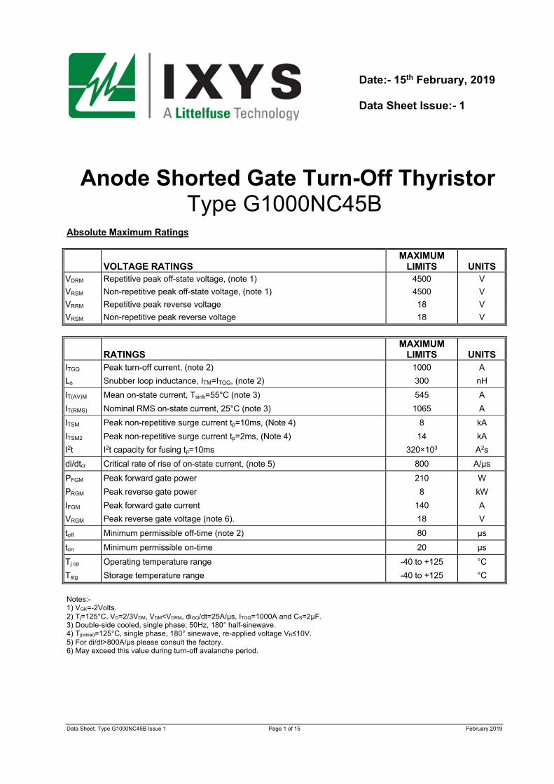
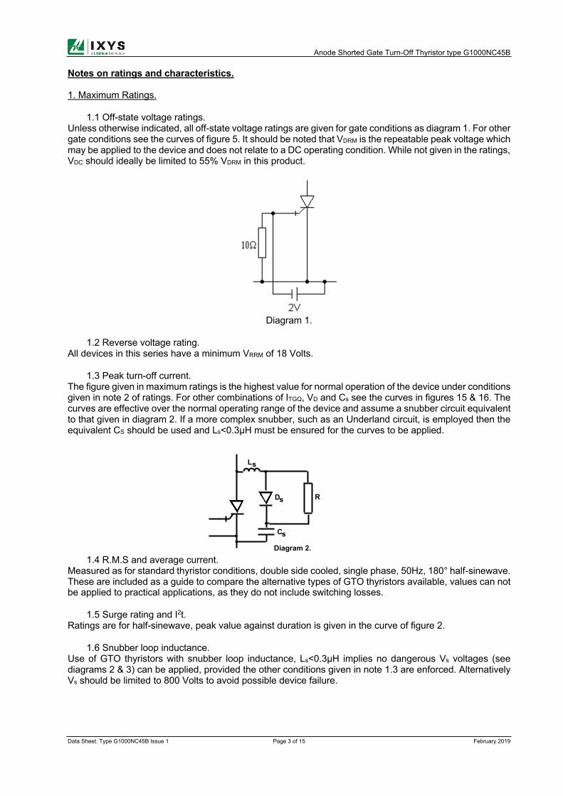
Unless otherwise indicated, all off-state voltage ratings are given for gate conditions as diagram 1. For other
gate conditions see the curves of figure 5. It should be noted that VDRM is the repeatable peak voltage which
may be applied to the device and does not relate to a DC operating condition. While not given in the ratings,
VDC should ideally be limited to 55% VDRM in this product.
Diagram 1.
1.2 Reverse voltage rating.
All devices in this series have a minimum VRRM of 18 Volts.
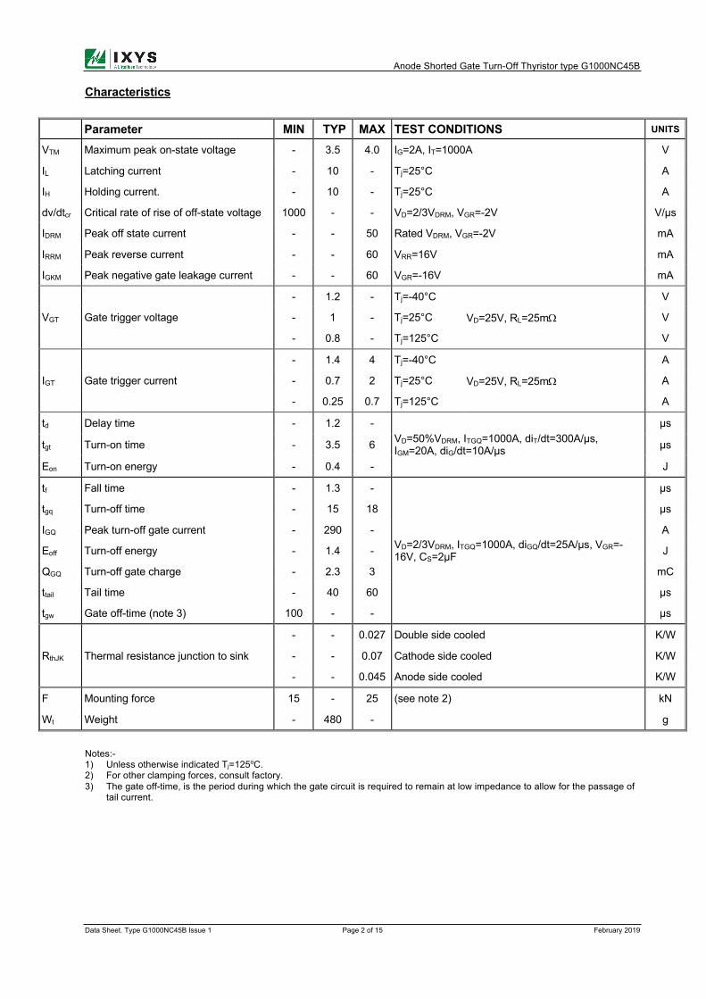
1.3 Peak turn-off current.
The figure given in maximum ratings is the highest value for normal operation of the device under conditions
given in note 2 of ratings. For other combinations of ITGQ, VD and Cs see the curves in figures 15 & 16. The
curves are effective over the normal operating range of the device and assume a snubber circuit equivalent
to that given in diagram 2. If a more complex snubber, such as an Underland circuit, is employed then the
equivalent CS should be used and Ls<0.3µH must be ensured for the curves to be applied.
1.4 R.M.S and average current.
Measured as for standard thyristor conditions, double side cooled, single phase, 50Hz, 180° half-sinewave.
These are included as a guide to compare the alternative types of GTO thyristors available, values can not
be applied to practical applications, as they do not include switching losses.
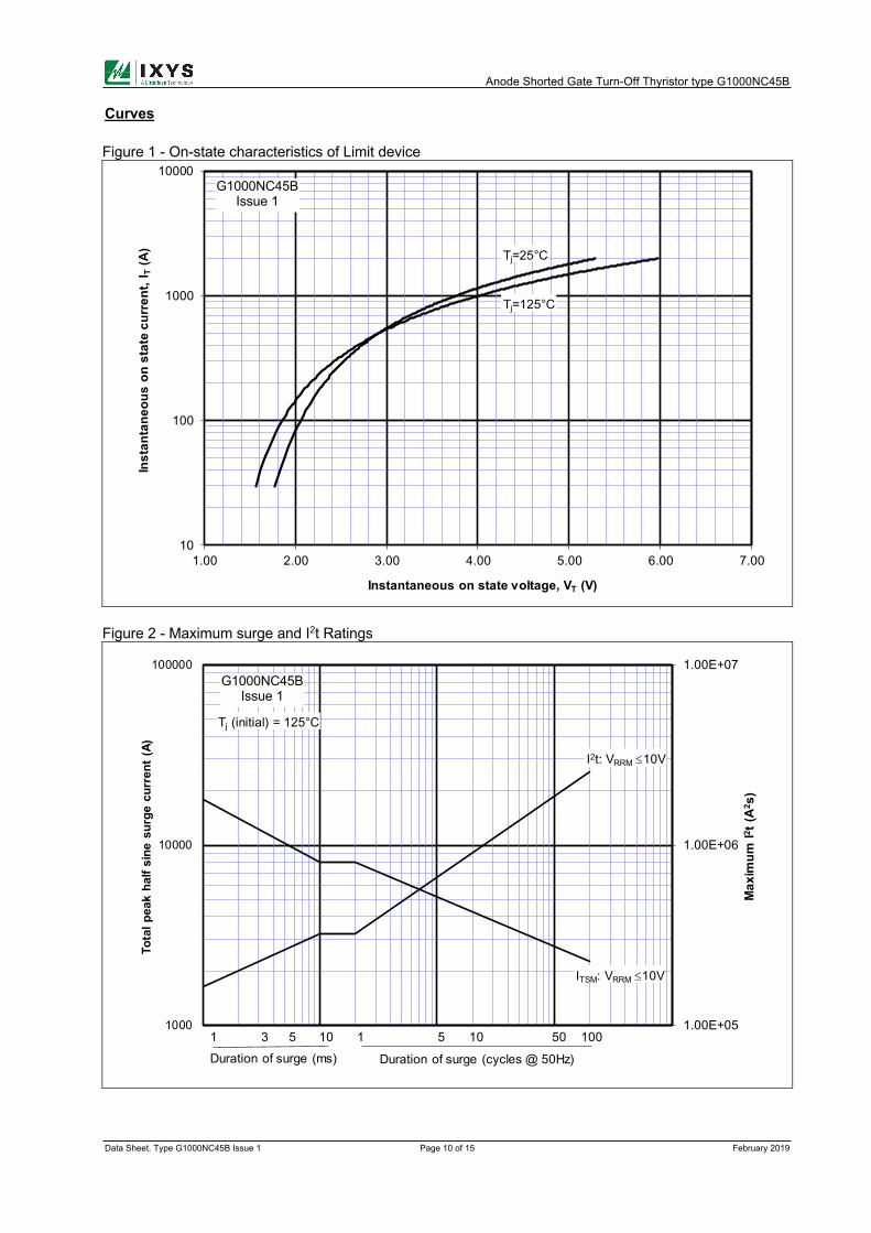
1.5 Surge rating and I2t.
Ratings are for half-sinewave, peak value against duration is given in the curve of figure 2.
1.6 Snubber loop inductance.
Use of GTO thyristors with snubber loop inductance, Ls<0.3µH implies no dangerous Vs voltages (see
diagrams 2 & 3) can be applied, provided the other conditions given in note 1.3 are enforced. Alternatively
Vs should be limited to 800 Volts to avoid possible device failure.
Ls
Ds R
Cs
Diagram 2.
Anode Shorted Gate Turn-Off Thyristor type G1000NC45B
Data Sheet. Type G1000NC45B Issue 1 Page 4 of 15 February 2019
1.7 Critical rate of rise of on-state current
The value given is the maximum repetitive rating, but does not imply any specific operating condition. The
high turn-on losses associated with limit di/dt would not allow for practical duty cycle at this maximum
condition. For special pulse applications, such as crowbars and pulse power supplies, a much higher di/dt
is possible. Where the device is required to operate with infrequent high current pulses, with natural
commutation (i.e. not gate turn-off), then di/dt>5kA/µs is possible. For this type of operation individual
specific evaluation is required.
1.8 Gate ratings
The absolute conditions above which the gate may be damaged. It is permitted to allow VGK(AV) during turn-
off to exceed VRGM which is the implied DC condition.
1.9 Minimum permissible off time.
This time relates specifically to re-firing of device (see also note on gate-off time 2.7). The value given in
the ratings applies only to operating conditions of ratings note 2.
1.10 Minimum permissible on-time.
Figure is given for minimum time to allow complete conduction of all the GTO thyristor islands. Where a
simple snubber, of the form given in diagram 1. (or any other non-energy recovery type which discharges
through the GTO at turn-on) the actual minimum on-time will usually be fixed by the snubber circuit time
constant, which must be allowed to fully discharge before the GTO thyristor is turned off. If the anode circuit
has di/dt<10A/µs then the minimum on-time should be increased, the actual value will depend upon the
di/dt and operating conditions (each case needs to be assessed on an individual basis).
Anode Shorted Gate Turn-Off Thyristor type G1000NC45B
Data Sheet. Type G1000NC45B Issue 1 Page 5 of 15 February 2019
2 Characteristics
2.1 Instantaneous on-state voltage
Measured using a 500µs square pulse, see also the curves of figure 1 for other values of ITM.
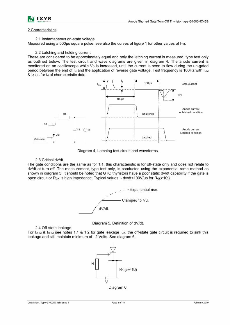
2.2 Latching and holding current
These are considered to be approximately equal and only the latching current is measured, type test only
as outlined below. The test circuit and wave diagrams are given in diagram 4. The anode current is
monitored on an oscilloscope while VD is increased, until the current is seen to flow during the un-gated
period between the end of IG and the application of reverse gate voltage. Test frequency is 100Hz with IGM & IG as for td of characteristic data.
Diagram 4, Latching test circuit and waveforms.
2.3 Critical dv/dt
The gate conditions are the same as for 1.1, this characteristic is for off-state only and does not relate to
dv/dt at turn-off. The measurement, type test only, is conducted using the exponential ramp method as
shown in diagram 5. It should be noted that GTO thyristors have a poor static dv/dt capability if the gate is
open circuit or RGK is high impedance. Typical values: - dv/dt<100V/µs for RGK>10W.
Diagram 5, Definition of dV/dt.
2.4 Off-state leakage.
For IDRM & IRRM see notes 1.1 & 1.2 for gate leakage IGK, the off-state gate circuit is required to sink this
leakage and still maintain minimum of –2 Volts. See diagram 6.
Diagram 6.
Gate-drive
R1
C1
CT
DUT
Vs
Gate current
16V
IG 100µs
100µs
IGM
Unlatched
Latched
Anode currentunlatched condition
Anode currentLatched condition
Anode Shorted Gate Turn-Off Thyristor type G1000NC45B
Data Sheet. Type G1000NC45B Issue 1 Page 6 of 15 February 2019
2.5 Gate trigger characteristics.
These are measured by slowly ramping up the gate current and monitoring the transition of anode current
and voltage (see diagram 7). Maximum and typical data of gate trigger current, for the full junction
temperature range, is given in the curves of figure 6. Only typical figures are given for gate trigger voltage,
however, the curves of figure 3 give the range of gate forward characteristics, for the full allowable junction
temperature range. The curves of figures 3 & 6 should be used in conjunction, when considering forward
gate drive circuit requirement. The gate drive requirements should always be calculated for lowest junction
temperature start-up condition.
Diagram 7, Gate trigger circuit and waveforms.
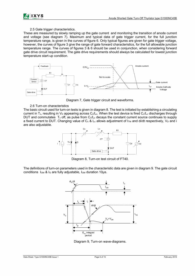
2.6 Turn-on characteristics
The basic circuit used for turn-on tests is given in diagram 8. The test is initiated by establishing a circulating
current in Tx, resulting in VD appearing across Cc/Lc. When the test device is fired Cc/Lc discharges through
DUT and commutates Tx off, as pulse from Cc/Lc decays the constant current source continues to supply
a fixed current to DUT. Changing value of Cc & Lc allows adjustment of ITM and di/dt respectively, VD and i
are also adjustable.
Diagram 8, Turn-on test circuit of FT40.
The definitions of turn-on parameters used in the characteristic data are given in diagram 9. The gate circuit
conditions IGM & IG are fully adjustable, IGM duration 10µs.
Diagram 9, Turn-on wave-diagrams.
Gate-drive
R1
C1
CT
DUT
Vs
Current-sence
Feedback Anode current
Gate current
Anode-CathodeVoltage
Not to scale
IGT
0.9VAK
0.1IA
Gate-drive
R1
Cd
CT
DUT
Vd
LcCc
DTxi
IGIGM
diG/dt
ITM
VD=VDM
trtd
tgt
Eon integralperiod
di/dt
VD
Anode Shorted Gate Turn-Off Thyristor type G1000NC45B
Data Sheet. Type G1000NC45B Issue 1 Page 7 of 15 February 2019
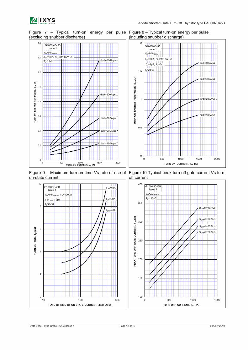
In addition to the turn-on time figures given in the characteristics data, the curves of figure 9 give the
relationship of tgt to di/dt and IGM. The data in the curves of figures 7 & 8, gives the turn-on losses both with
and without snubber discharge, a snubber of the form given in diagram 2 is assumed. Only typical losses
are given due to the large number of variables which effect Eon. It is unlikely that all negative aspects would
appear in any one application, so typical figures can be considered as worst case. Where the turn-on loss
is higher than the figure given it will in most cases be compensated by reduced turn-off losses, as variations
in processing inversely effect many parameters. For a worst case device, which would also have the lowest
turn-off losses, Eon would be 1.5x values given in the curves of figures 7 & 8. Turn-on losses are measured
over the integral period specified below:-
The turn-on loss can be sub-divided into two component parts, firstly that associated with tgt and secondly
the contribution of the voltage tail. For this series of devices tgt contributes 40% and the voltage tail 60%
(These figures are approximate and are influenced by several second order effects). The loss during tgt is
greatly affected by gate current and as with turn-on time (figure 9), it can be reduced by increasing IGM. The
turn-on loss associated with the voltage tail is not effected by the gate conditions and can only be reduced
by limiting di/dt, where appropriate a turn-on snubber should be used. In applications where the snubber is
discharged through the GTO thyristor at turn-on, selection of discharge resistor will effect Eon. The curves
of figure 8 are given for a snubber as shown in diagram 2, with R=5W, this is the lowest recommended
value giving the highest Eon, higher values will reduce Eon.
2.7 Turn-off characteristics
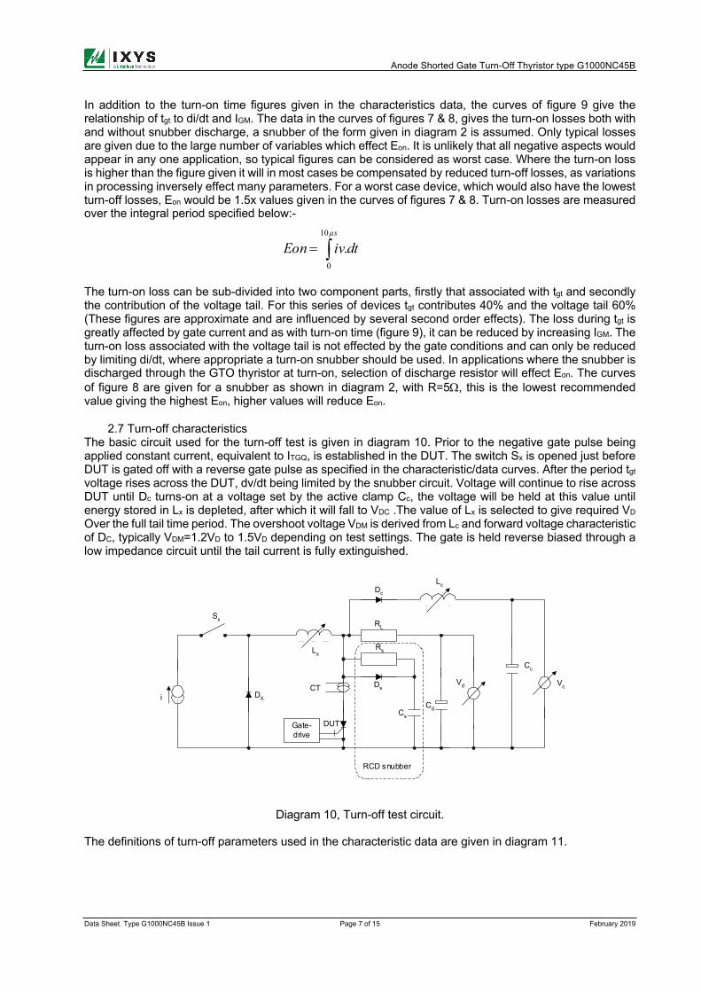
The basic circuit used for the turn-off test is given in diagram 10. Prior to the negative gate pulse being
applied constant current, equivalent to ITGQ, is established in the DUT. The switch Sx is opened just before
DUT is gated off with a reverse gate pulse as specified in the characteristic/data curves. After the period tgt
voltage rises across the DUT, dv/dt being limited by the snubber circuit. Voltage will continue to rise across
DUT until Dc turns-on at a voltage set by the active clamp Cc, the voltage will be held at this value until
energy stored in Lx is depleted, after which it will fall to VDC .The value of Lx is selected to give required VD
Over the full tail time period. The overshoot voltage VDM is derived from Lc and forward voltage characteristic
of DC, typically VDM=1.2VD to 1.5VD depending on test settings. The gate is held reverse biased through a
low impedance circuit until the tail current is fully extinguished.
Diagram 10, Turn-off test circuit.
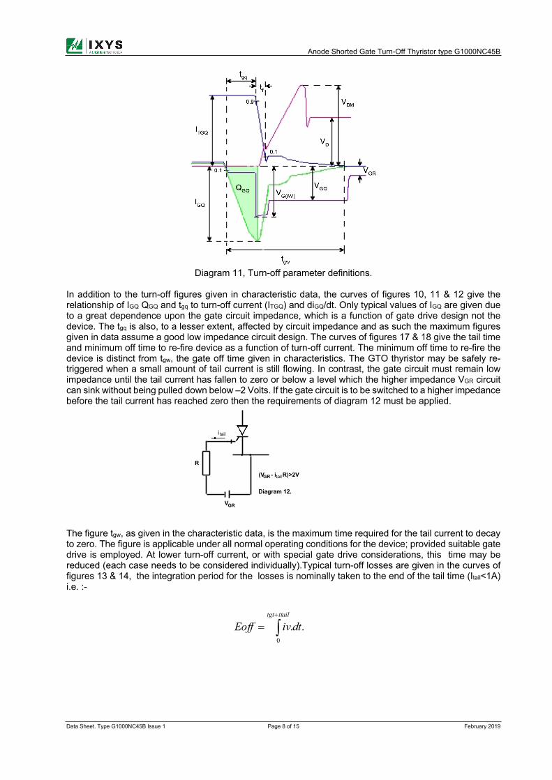
The definitions of turn-off parameters used in the characteristic data are given in diagram 11.
ò=µs
dtivEon10
0
.
Gate-drive
RL
Cd
CT
DUT
Vd
Lx
Sx
DXi
Rs
Cs
Ds
Dc
Lc
Vc
Cc
RCD snubber
Anode Shorted Gate Turn-Off Thyristor type G1000NC45B
Data Sheet. Type G1000NC45B Issue 1 Page 8 of 15 February 2019
Diagram 11, Turn-off parameter definitions.
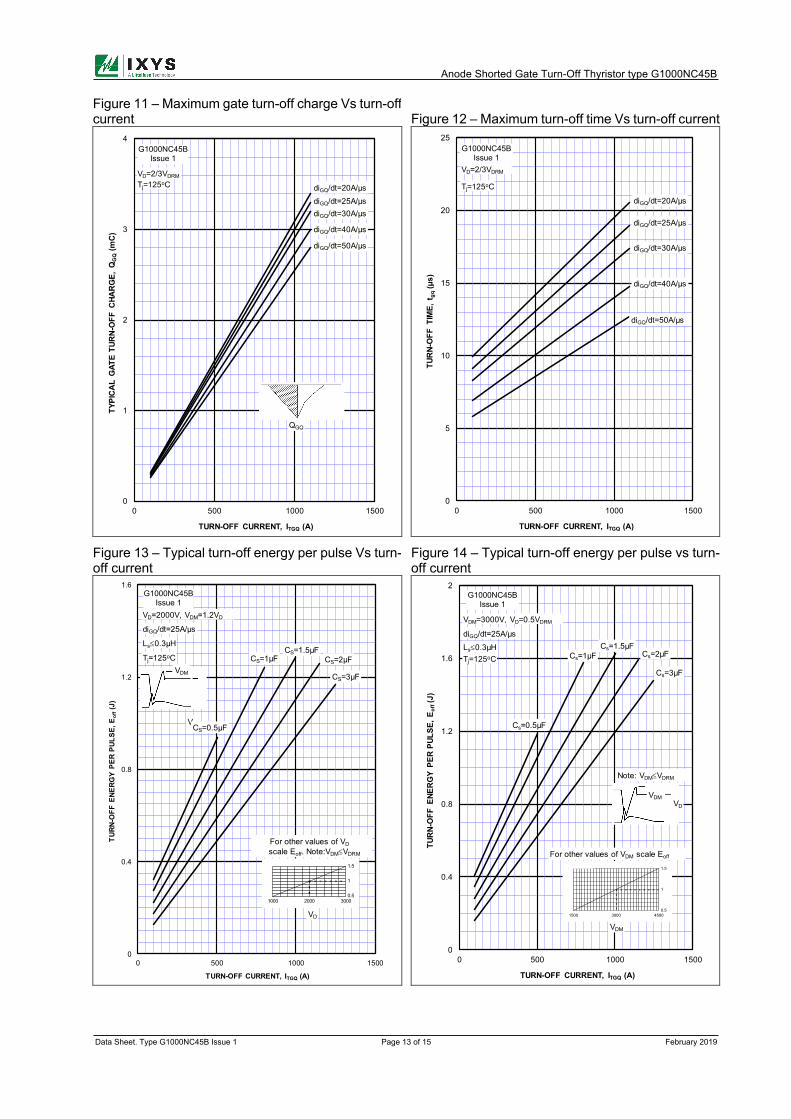
In addition to the turn-off figures given in characteristic data, the curves of figures 10, 11 & 12 give the
relationship of IGQ QGQ and tgq to turn-off current (ITGQ) and diGQ/dt. Only typical values of IGQ are given due
to a great dependence upon the gate circuit impedance, which is a function of gate drive design not the
device. The tgq is also, to a lesser extent, affected by circuit impedance and as such the maximum figures
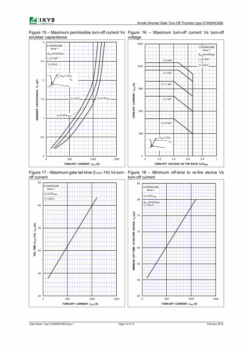
given in data assume a good low impedance circuit design. The curves of figures 17 & 18 give the tail time
and minimum off time to re-fire device as a function of turn-off current. The minimum off time to re-fire the
device is distinct from tgw, the gate off time given in characteristics. The GTO thyristor may be safely re-
triggered when a small amount of tail current is still flowing. In contrast, the gate circuit must remain low
impedance until the tail current has fallen to zero or below a level which the higher impedance VGR circuit
can sink without being pulled down below –2 Volts. If the gate circuit is to be switched to a higher impedance
before the tail current has reached zero then the requirements of diagram 12 must be applied.
The figure tgw, as given in the characteristic data, is the maximum time required for the tail current to decay
to zero. The figure is applicable under all normal operating conditions for the device; provided suitable gate
drive is employed. At lower turn-off current, or with special gate drive considerations, this time may be
reduced (each case needs to be considered individually).Typical turn-off losses are given in the curves of
figures 13 & 14, the integration period for the losses is nominally taken to the end of the tail time (Itail<1A)
i.e. :-
ò+
=ttailtgt
dtivEoff0
..
R
V
Diagram 12.
i tail
GR
(V - i R)>2VGR tail
Anode Shorted Gate Turn-Off Thyristor type G1000NC45B
Data Sheet. Type G1000NC45B Issue 1 Page 9 of 15 February 2019
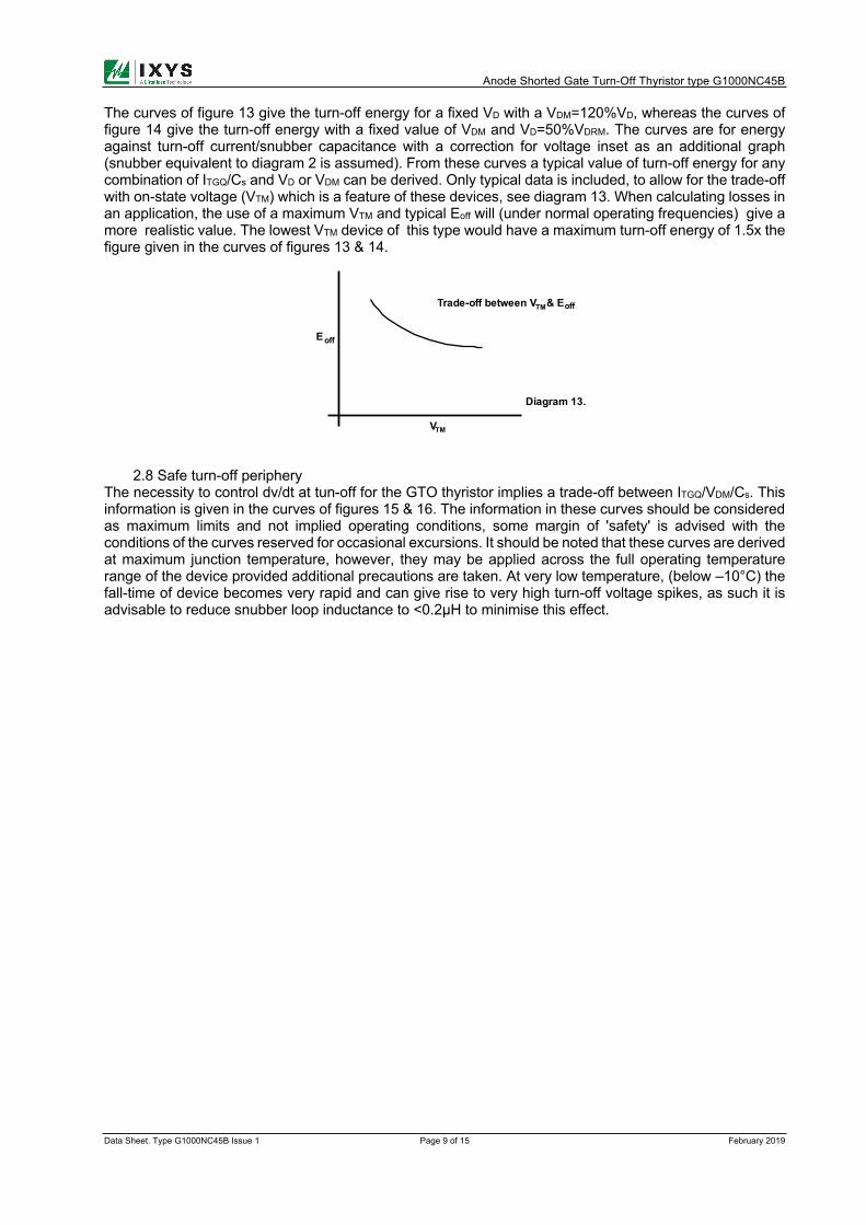
The curves of figure 13 give the turn-off energy for a fixed VD with a VDM=120%VD, whereas the curves of
figure 14 give the turn-off energy with a fixed value of VDM and VD=50%VDRM. The curves are for energy
against turn-off current/snubber capacitance with a correction for voltage inset as an additional graph
(snubber equivalent to diagram 2 is assumed). From these curves a typical value of turn-off energy for any
combination of ITGQ/Cs and VD or VDM can be derived. Only typical data is included, to allow for the trade-off
with on-state voltage (VTM) which is a feature of these devices, see diagram 13. When calculating losses in
an application, the use of a maximum VTM and typical Eoff will (under normal operating frequencies) give a
more realistic value. The lowest VTM device of this type would have a maximum turn-off energy of 1.5x the
figure given in the curves of figures 13 & 14.
2.8 Safe turn-off periphery
The necessity to control dv/dt at tun-off for the GTO thyristor implies a trade-off between ITGQ/VDM/Cs. This
information is given in the curves of figures 15 & 16. The information in these curves should be considered
as maximum limits and not implied operating conditions, some margin of 'safety' is advised with the
conditions of the curves reserved for occasional excursions. It should be noted that these curves are derived
at maximum junction temperature, however, they may be applied across the full operating temperature
range of the device provided additional precautions are taken. At very low temperature, (below –10°C) the
fall-time of device becomes very rapid and can give rise to very high turn-off voltage spikes, as such it is
advisable to reduce snubber loop inductance to <0.2µH to minimise this effect.
Eoff
VTM
Diagram 13.
Trade-off between V & ETM off
Anode Shorted Gate Turn-Off Thyristor type G1000NC45B
Data Sheet. Type G1000NC45B Issue 1 Page 10 of 15 February 2019
Curves
Figure 1 - On-state characteristics of Limit device
Figure 2 - Maximum surge and I2t Ratings
10
100
1000
10000
1.00 2.00 3.00 4.00 5.00 6.00 7.00
Inst
anta
neou
s on
sta
te c
urre
nt, I
T(A
)
Instantaneous on state voltage, VT (V)
Tj=25°C
Tj=125°C
1000
10000
100000
1.00E+05
1.00E+06
1.00E+07
Tota
l pea
k ha
lf si
ne s
urge
cur
rent
(A)
Max
imum
I2t (
A2 s
)
1 3 5 10 1 5 10 50 100
Duration of surge (ms) Duration of surge (cycles @ 50Hz)
I2t: VRRM £10V
ITSM: VRRM £10V
Tj (initial) = 125°C
G1000NC45B
Issue 1
G1000NC45B
Issue 1
Anode Shorted Gate Turn-Off Thyristor type G1000NC45B
Data Sheet. Type G1000NC45B Issue 1 Page 11 of 15 February 2019
Figure 3 – Forward gate characteristics Figure 4 – Transient thermal impedance
Figure 5 – Typical forward blocking voltage vs.
external gate-cathode resistance Figure 6 – Gate trigger current vs. junction
temperature
1
10
100
1000
0 0.5 1 1.5 2
INST
ANTA
NEO
US F
ORW
ARD
GAT
E CU
RREN
T, I
FG(A
)
INSTANTANEOUS FORWARD GATE VOLTAGE, VFG (V)
FOR Tj=-40oC TO +125oC
MINIMUM MAXIMUM
0.0001
0.001
0.01
0.1
0.001 0.01 0.1 1 10 100
THER
MAL
IMPE
DANC
E JU
NCTI
ON
TO S
INK
R thJ
K, (
K/W
)
TIME, (S)
CATHODE
ANODE
DOUBLE-SIDE
0
0.2
0.4
0.6
0.8
1
1.2
1 10 100 1000
FORW
ARD
BLO
CKIN
G A
S A
RATI
O O
F V D
/VD
RM
EXTERNAL GATE-CATHODE RESISTANCE, RGK (W)
Tj=50oC
Tj=125oC
Tj=105oC
Tj=80oC
0.1
1
10
-50 -25 0 25 50 75 100 125 150
D.C.
GAT
E TR
IGG
ER C
URRE
NT,
I GT
(A)
JUNCTION TEMPERATURE, Tj(oC)
MAXIMUM
TYPICAL
G1000NC45B
Issue 1
G1000NC45B
Issue 1
G1000NC45B
Issue 1
G1000NC45B
Issue 1
Anode Shorted Gate Turn-Off Thyristor type G1000NC45B
Data Sheet. Type G1000NC45B Issue 1 Page 12 of 15 February 2019
Figure 7 – Typical turn-on energy per pulse
(excluding snubber discharge) Figure 8 – Typical turn-on energy per pulse
(including snubber discharge)
Figure 9 – Maximum turn-on time Vs rate of rise of
on-state current Figure 10 Typical peak turn-off gate current Vs turn-
off current
0
0.2
0.4
0.6
0.8
1
1.2
1.4
1.6
0 500 1000 1500 2000
TUR
N-O
N E
NER
GY
PER
PU
LSE,
EO
N(J
)
TURN-ON CURRENT, ITM (A)
VD=0.5VDRM
Tj=25oC
di/dt=200A/µs
di/dt=300A/µs
IGM=20A, diGQ/dt=10A/ µs
di/dt=100A/µs
di/dt=400A/µs
di/dt=500A/µs
0
0.5
1
1.5
2
0 500 1000 1500 2000
TURN
-ON
ENER
GY
PER
PULS
E, E
ON
(J)
TURN-ON CURRENT, ITM (A)
VD=0.5VDRM
Tj=25oC
di/dt=200A/µs
di/dt=300A/µs
IGM=20A, diG/dt=10A/ µs
di/dt=100A/µs
di/dt=400A/µsCs=2µF, Rs=5W
0
2
4
6
8
10
10 100 1000
TURN
-ON
TIM
E, t
gt(µ
s)
RATE OF RISE OF ON-STATE CURRENT, di/dt (A/ µs)
VD=0.5VDRM, ITM=1000A
tr of IGM £ 2µsTj=25oC
IGM=10A
IGM=40A
IGM=20A
100
150
200
250
300
350
400
0 500 1000 1500
PEAK
TUR
N-O
FF G
ATE
CURR
ENT,
IG
Q(A
)
TURN-OFF CURRENT, ITGQ (A)
VD=2/3VDRMTj=125oC
diGQ/dt=30A/µs
diGQ/dt=20A/µs
diGQ/dt=40A/µs
diGQ/dt=25A/µs
G1000NC45B
Issue 1 G1000NC45B
Issue 1
G1000NC45B
Issue 1
G1000NC45B
Issue 1
Anode Shorted Gate Turn-Off Thyristor type G1000NC45B
Data Sheet. Type G1000NC45B Issue 1 Page 13 of 15 February 2019
Figure 11 – Maximum gate turn-off charge Vs turn-off
current Figure 12 – Maximum turn-off time Vs turn-off current
Figure 13 – Typical turn-off energy per pulse Vs turn-
off current Figure 14 – Typical turn-off energy per pulse vs turn-
off current
0
1
2
3
4
0 500 1000 1500
TYPI
CAL
GAT
E TU
RN-O
FF C
HARG
E, Q
GQ
(mC)
TURN-OFF CURRENT, ITGQ (A)
VD=2/3VDRMTj=125oC
QGQ
diGQ/dt=30A/µs
diGQ/dt=20A/µs
diGQ/dt=50A/µs
diGQ/dt=40A/µs
diGQ/dt=25A/µs
0
5
10
15
20
25
0 500 1000 1500
TURN
-OFF
TIM
E, t
gq(µ
s)
TURN-OFF CURRENT, ITGQ (A)
VD=2/3VDRM
Tj=125oC
diGQ/dt=40A/µs
diGQ/dt=50A/µs
diGQ/dt=30A/µs
diGQ/dt=20A/µs
diGQ/dt=25A/µs
0
0.4
0.8
1.2
1.6
0 500 1000 1500
TURN
-OFF
ENE
RGY
PER
PULS
E, E
off(J
)
TURN-OFF CURRENT, ITGQ (A)
VD
For other values of VDscale Eoff. Note:VDM£VDRM
VD=2000V, VDM=1.2VD
diGQ/dt=25A/µs
Ls£0.3µH
Tj=125oCVDM
VDCS=0.5µF
CS=3µF
CS=1µF CS=2µFCS=1.5µF
0.5
1
1.5
1000 2000 3000
0
0.4
0.8
1.2
1.6
2
0 500 1000 1500
TURN
-OFF
ENE
RGY
PER
PULS
E, E
off (
J)
TURN-OFF CURRENT, ITGQ (A)
VDM=3000V, VD=0.5VDRM
diGQ/dt=25A/µsLs£0.3µHTj=125oC
VDM
VDMVD
Cs=1.5µF
For other values of VDM scale Eoff
Note: VDM£VDRM
Cs=2µF
Cs=0.5µF
Cs=1µF
Cs=3µF
0.5
1
1.5
1500 3000 4500
G1000NC45B
Issue 1
G1000NC45B
Issue 1
G1000NC45B
Issue 1 G1000NC45B
Issue 1
Anode Shorted Gate Turn-Off Thyristor type G1000NC45B
Data Sheet. Type G1000NC45B Issue 1 Page 14 of 15 February 2019
Figure 15 – Maximum permissible turn-off current Vs
snubber capacitance Figure 16 – Maximum turn-off current Vs turn-off
voltage
Figure 17 – Maximum gate tail time (ITGQ<1A) Vs turn-
off current Figure 18 – Minimum off-time to re-fire device Vs
turn-off current
0
0.5
1
1.5
2
2.5
3
0 500 1000 1500
SNUB
BER
CA
PAC
ITA
NCE,
Cs
(µF)
TURN-OFF CURRENT, ITGQ (A)
VD=2/3VDRM
VD=0.55VDRM
VD£0.4VDRM
diGQ/dt=25A/µs
Ls£0.3µH
Tj=125oC
VDM£1.5VDVD
0
300
600
900
1200
1500
0 0.2 0.4 0.6 0.8 1
TURN
-OFF
CUR
RENT
, I TG
Q(A
)
TURN-OFF VOLTAGE AS THE RATIO VD/VDRM
diGQ/dt=25A/µs
Ls<0.3µH
Tj=125oC
Cs=1µF
VDM£1.5VDVD
Cs=3µF
Cs=2µF
Cs=0.5µF
Cs=1.4µF
40
45
50
55
60
65
0 500 1000 1500
TAIL
TIM
E (I T
GQ<1
A),
t tail
(µs)
TURN-OFF CURRENT, ITGQ (A)
VD=2/3VDRM
Tj=125oC
50
55
60
65
70
75
80
85
0 500 1000 1500
MIN
IMUM
OFF
-TIM
E TO
RE-
FIRE
DEV
ICE,
tof
f(µs
)
TURN-OFF CURRENT, ITGQ (A)
VD=2/3VDRM
Tj=125oCdiGQ/dt=25A/µs
G1000NC45B
Issue 1 G1000NC45B
Issue 1
G1000NC45B
Issue 1 G1000NC45B
Issue 1
Anode Shorted Gate Turn-Off Thyristor type G1000NC45B
Data Sheet. Type G1000NC45B Issue 1 Page 15 of 15 February 2019
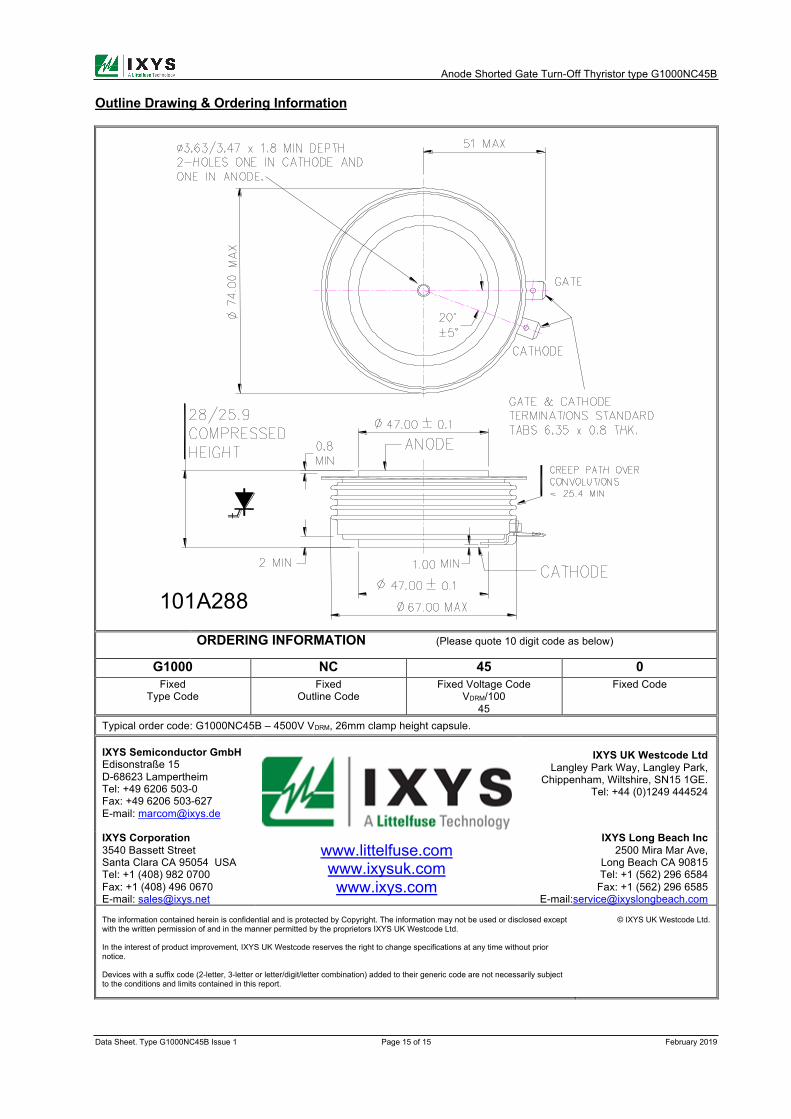
Outline Drawing & Ordering Information
ORDERING INFORMATION (Please quote 10 digit code as below)
G1000 NC 45 0 Fixed
Type Code
Fixed
Outline Code
Fixed Voltage Code
VDRM/100
45
Fixed Code
Typical order code: G1000NC45B – 4500V VDRM, 26mm clamp height capsule.
IXYS Semiconductor GmbH Edisonstraße 15
D-68623 Lampertheim
Tel: +49 6206 503-0
Fax: +49 6206 503-627
E-mail: [email protected]
IXYS UK Westcode Ltd
Langley Park Way, Langley Park,
Chippenham, Wiltshire, SN15 1GE.
Tel: +44 (0)1249 444524
IXYS Corporation 3540 Bassett Street
Santa Clara CA 95054 USA
Tel: +1 (408) 982 0700
Fax: +1 (408) 496 0670
E-mail: [email protected]
www.littelfuse.com
www.ixysuk.com
www.ixys.com
IXYS Long Beach Inc 2500 Mira Mar Ave,
Long Beach CA 90815
Tel: +1 (562) 296 6584
Fax: +1 (562) 296 6585
E-mail:[email protected]
The information contained herein is confidential and is protected by Copyright. The information may not be used or disclosed except
with the written permission of and in the manner permitted by the proprietors IXYS UK Westcode Ltd.
In the interest of product improvement, IXYS UK Westcode reserves the right to change specifications at any time without prior
notice.
Devices with a suffix code (2-letter, 3-letter or letter/digit/letter combination) added to their generic code are not necessarily subject
to the conditions and limits contained in this report.
© IXYS UK Westcode Ltd.
101A288

Disclaimer Notice - Information furnished is believed to be accurate and reliable. However, users should independently evaluate the suitability of and test each product selected for their own applications. Littelfuse products are not designed for, and may not be used in, all applications. Read complete Disclaimer Notice at www.littelfuse.com/disclaimer-electronics.


![Digital Logic LAB Manual KL-300 [Shorted]](https://static.fdocuments.us/doc/165x107/55cf93ef550346f57b9ed2c2/digital-logic-lab-manual-kl-300-shorted.jpg)